MATERIALS RESEARCH CENTRE MATERIALS RESEARCH CENTRE MALAVIYA NATIONAL INSTITUTE OF MALAVIYA NATIONAL INSTITUTE OF TECHNOLOGY, JAIPUR TECHNOLOGY, JAIPUR J.L.N J.L.N Marg Marg, Jaipur, Rajasthan (INDIA) , Jaipur, Rajasthan (INDIA)
Transcript
MATERIALS RESEARCH CENTREMATERIALS RESEARCH CENTREMALAVIYA NATIONAL INSTITUTE OFMALAVIYA NATIONAL INSTITUTE OF
Materials Research CentreMalaviya National Institute of Technology Jaipur
Transmission Electron Microscope1. The Tecnai G2 20 (FEI) S-Twin is a 200 kV transmission
electron microscope designed to offer high resolutionimaging and analysis solution for life sciences,materials science, nanotechnology and thesemiconductor and data storage industries.
2. The Tecnai G2 supports a wide range of techniquesincluding high resolution scanning S/TEM diffractionand chemical analysis. The on axis BF/DF detectorsprovide the Z-contrast imaging.
3. The high angle, annular dark field detector generatesatomic resolution dark field STEM images. Theequipment provides a point resolution of 0.24 nm, lineresolution of 0.14 nm and STEM resolution of 1.0 nm.EDAX gives the elemental composition of material.
1. The Tecnai G2 20 (FEI) S-Twin is a 200 kV transmissionelectron microscope designed to offer high resolutionimaging and analysis solution for life sciences,materials science, nanotechnology and thesemiconductor and data storage industries.
2. The Tecnai G2 supports a wide range of techniquesincluding high resolution scanning S/TEM diffractionand chemical analysis. The on axis BF/DF detectorsprovide the Z-contrast imaging.
3. The high angle, annular dark field detector generatesatomic resolution dark field STEM images. Theequipment provides a point resolution of 0.24 nm, lineresolution of 0.14 nm and STEM resolution of 1.0 nm.EDAX gives the elemental composition of material.
1. Multimode Scanning Probe Microscope (Bruker) hasall standard operating modes like SPM, AFM, MFM,LFM, TM, TR nanoindentation, lithography and manyunique capabilities to characterize everything frommechanical to electrical properties at highresolution.
1. Multimode Scanning Probe Microscope (Bruker) hasall standard operating modes like SPM, AFM, MFM,LFM, TM, TR nanoindentation, lithography and manyunique capabilities to characterize everything frommechanical to electrical properties at highresolution.
Applications:•Electrical property mapping (current and capacitance)•Direct mapping of nanomechanical properties, including elastic modulus, adhesion and dissipation, at high resolution andnormal scan rates
2. Advanced optics & detection, including beamdeceleration, in lens ETD(SE), TLD (custom), lensmounted DBS & LVD offer best selection ofinformation & image optimization. Beam landingenergy can go down from 30 keV to 50 eV.
3. It gives a resolution of 1.4 nm at 1 kV (TLD-SE) & 1nm at 15 kV (TLD-SE). The FE-SEM is coupled to EDAXdetector for measuring the elemental chemicalcomposition of materials.
Applications:•Metallic materials•Ceramics and composites•Polymeric materials•Geology and mineralogy•Dental materials
X-Ray Diffractometer
1. The X-Ray Diffractometer (Panalytical X Pert Pro) is aversatile equipment designed for a wide variety ofapplications in X-ray diffraction analysis on powders,thin films, epitaxial layers, machined materials,ceramics etc.
2. The use of pre FIX optical modules, sample platform &tube rotation feature enable the user to change thesystem from a high resolution or stress texture pointfocus application to a normal Bragg-Brentano linefocus configuration or a reflectrometry system.
1. ECS 400 MHz (JEOL) NMR spectrometer is a 2-channel console with a flexible broad band RFperformance.
2. Capable of providing spectra of a variety of NMR-active nuclei such as 1H, 13C, 19F and metals like Sn, Cuin distinct chemical environments without any timedelay. Low temperature accessory permits variabletemperature.
Applications:•Determination of the content and purity of a sample through space connectivity (Overhausereffect)•Chemical dynamics (Line shapes, relaxation phenomena)•1 D,2D (COSY,NOSY,HETCOR,DEPT HMQC etc.)
Mass Spectrometer1. Xevo G2-S Q Tof (Waters, USA) provides a wide
range of mass analysis of small organic/inorganic/organometallic compounds to large polymeric &proteomics samples including proteins & peptides.
2. The Q Tof technology in this instrument providessuperior UPLC-compatible mass resolution, matrix-tolerant dynamic range, quantitative performance,simultaneous mass accuracy and speed of analysis.Fast data directed analysis allows full structuralcharacterization of unknown compounds.
3. The UPLC/MS data acquisition comprehensivelycatalogs complex samples in a single analysis.Universal Ion Source Architecture enables the mostextensive range of interface capabilities to service thebroadest range of applications.
4. LC/MS, MS/MS, HRMS analysis of liquid and samplesup to a range of m/z 1,00,000 is available with detailmass analysis.
1. Xevo G2-S Q Tof (Waters, USA) provides a widerange of mass analysis of small organic/inorganic/organometallic compounds to large polymeric &proteomics samples including proteins & peptides.
2. The Q Tof technology in this instrument providessuperior UPLC-compatible mass resolution, matrix-tolerant dynamic range, quantitative performance,simultaneous mass accuracy and speed of analysis.Fast data directed analysis allows full structuralcharacterization of unknown compounds.
3. The UPLC/MS data acquisition comprehensivelycatalogs complex samples in a single analysis.Universal Ion Source Architecture enables the mostextensive range of interface capabilities to service thebroadest range of applications.
4. LC/MS, MS/MS, HRMS analysis of liquid and samplesup to a range of m/z 1,00,000 is available with detailmass analysis.Applications:
•Environmental•Life Sciences and Pharmaceuticals•Chemical•Food
Abrasive Cutter
1. The AbrasiMatic® 300 (Buehler) abrasive cutter is abench-top cutter featuring manual cutting action in3 directions & automated cutting in 1 direction.
2. This gives the user the maximum versatility tosection a wide variety of sample materials, sizes andgeometries. It is engineered with innovativecapabilities to be used in both production supportand laboratory environments.
Applications:Cutting of :•steel•highly-alloyed metals•coated metals•ceramics•concrete and minerals
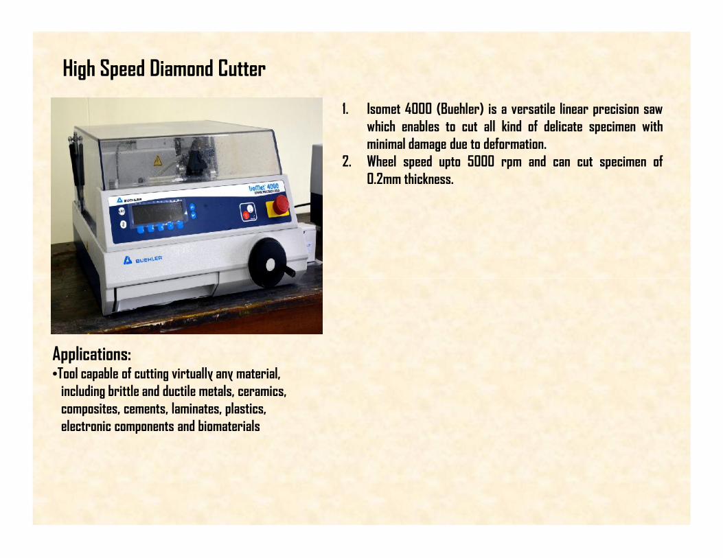
High Speed Diamond Cutter
1. Isomet 4000 (Buehler) is a versatile linear precision sawwhich enables to cut all kind of delicate specimen withminimal damage due to deformation.
2. Wheel speed upto 5000 rpm and can cut specimen of0.2mm thickness.
Applications:•Tool capable of cutting virtually any material,
including brittle and ductile metals, ceramics,composites, cements, laminates, plastics,electronic components and biomaterials
Hot Mounting Press
1. Simplimet 3000 (Buehler) Automatic MountingPress is a durable press with basic features thatprovide effective mounting, increases productivityand specimen consistency verses manual mountingpress.
2. Electrohydraulic operation requires no air.Enhanced features include 25 user definablemethods and thermoplastic parameters.
Applications:•Can mount Metallurgical, Petro graphic and other
Materials for Micro structural Analysis
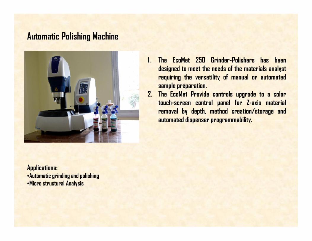
Automatic Polishing Machine
1. The EcoMet 250 Grinder-Polishers has beendesigned to meet the needs of the materials analystrequiring the versatility of manual or automatedsample preparation.
2. The EcoMet Provide controls upgrade to a colortouch-screen control panel for Z-axis materialremoval by depth, method creation/storage andautomated dispenser programmability.
Applications:•Automatic grinding and polishing•Micro structural Analysis
Semi-Automatic Polishing Machine
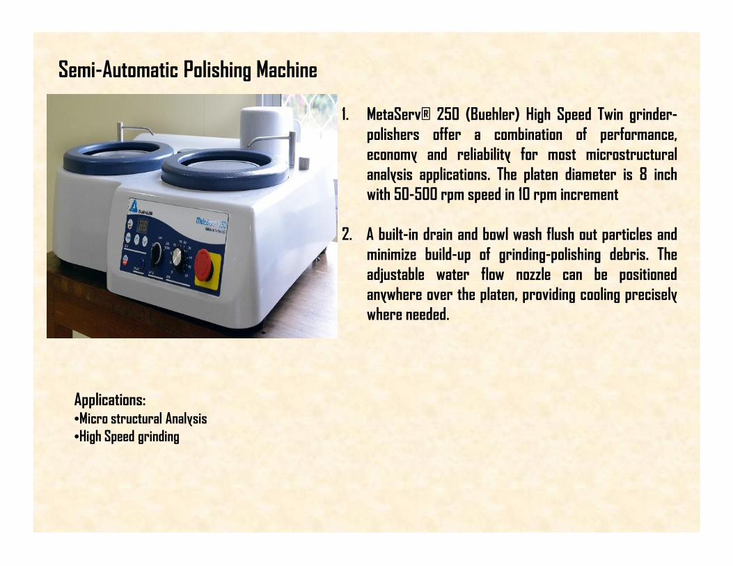
1. MetaServ® 250 (Buehler) High Speed Twin grinder-polishers offer a combination of performance,economy and reliability for most microstructuralanalysis applications. The platen diameter is 8 inchwith 50-500 rpm speed in 10 rpm increment
2. A built-in drain and bowl wash flush out particles andminimize build-up of grinding-polishing debris. Theadjustable water flow nozzle can be positionedanywhere over the platen, providing cooling preciselywhere needed.
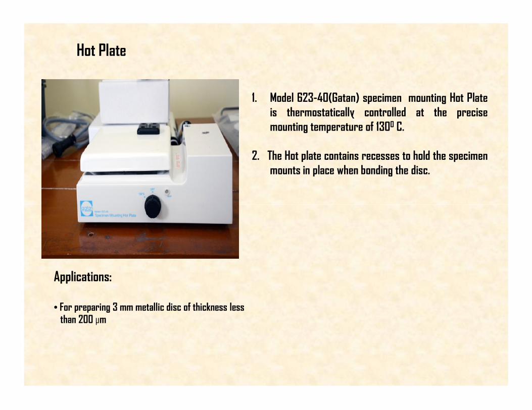
1. Model 623-40(Gatan) specimen mounting Hot Plateis thermostatically controlled at the precisemounting temperature of 1300 C.
2. The Hot plate contains recesses to hold the specimenmounts in place when bonding the disc.
Applications:
• For preparing 3 mm metallic disc of thickness lessthan 200 µm
Dimple Grinder With Stereomicroscope
1. Model 656 (Gatan) Dimple Grinder can reduce, withminimal damage, the central region of a typical 100μm thick, 3 mm diameter specimen blank to a fewmicrons in times ranging from 20 minutes forsilicon to 100 minutes for sapphire.
Applications:•Direct preparation of TEM Specimens•Micro positioning of specimens•Improved auger profiling for specimens•Accurate depth and thickness control for dimples
Ion Beam Milling
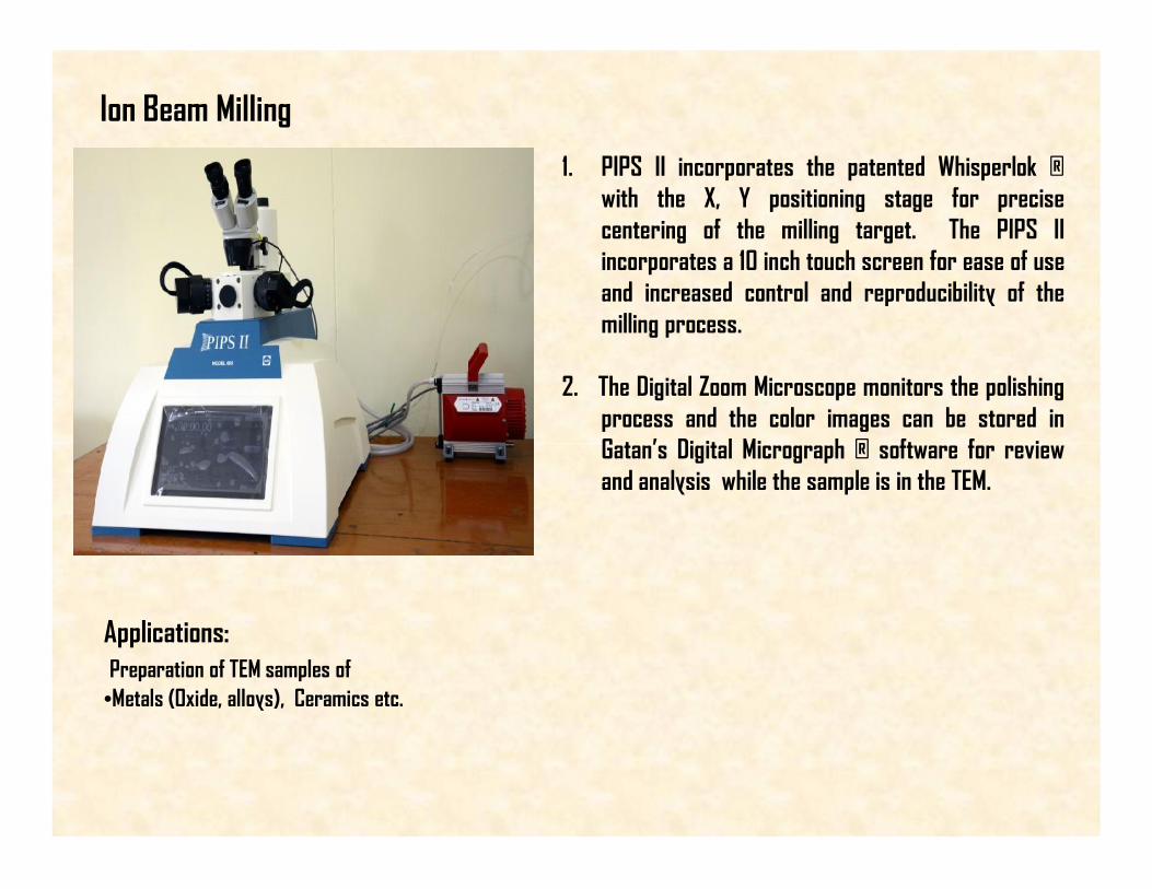
1. PIPS II incorporates the patented Whisperlok ®with the X, Y positioning stage for precisecentering of the milling target. The PIPS IIincorporates a 10 inch touch screen for ease of useand increased control and reproducibility of themilling process.
2. The Digital Zoom Microscope monitors the polishingprocess and the color images can be stored inGatan’s Digital Micrograph ® software for reviewand analysis while the sample is in the TEM.
Applications:Preparation of TEM samples of•Metals (Oxide, alloys), Ceramics etc.
Twin Jet Tenupol
1. TenuPol-5 (Struers) is capable of preparing aperforated specimen for transmission electronmicroscope from a sample of 3 mm diameter in justa few minutes.
2. The specimen is polished from both sidessimultaneously providing a structure with aminimum of deformation.
3. When the perforation appears, the polishing canautomatically be stopped by the infrared detectorsystem. Electrolytic pre-thinning or blanking canalso easily be carried out.
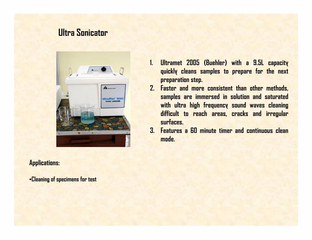
1. Ultramet 2005 (Buehler) with a 9.5L capacityquickly cleans samples to prepare for the nextpreparation step.
2. Faster and more consistent than other methods,samples are immersed in solution and saturatedwith ultra high frequency sound waves cleaningdifficult to reach areas, cracks and irregularsurfaces.
3. Features a 60 minute timer and continuous cleanmode.
Applications:
•Cleaning of specimens for test
Fluorescence Spectrometer
1. The LS 55 (Perkin Elmer) Fluorescencespectrometer provides all types of data applicationsthat require fluorescence, phosphorescence,bioluminescence, chemiluminescence etc. withexcitation range of 200-800nm.
Applications:•Cell based Cytotoxicity, cell viability, cell quantification, cell proliferation, adhesion, and reporter gene expression,apoptosis, Clinical Enzyme and substrate assays, porphyrins, steroids, blood flow.•Environmental Pesticide detection on many substrates including leaves, ground water tracing, oil contamination of freshand marine water, EROD assays, chlorophyll determination of normal and toxic algae.•Pharmaceutical Vitamins, biogenic amines, pharmaceutical and abuse drugs, toxicity assays, cell function assays.•Inorganic Aluminium, lead, magnesium, manganese, selenium, tin, zinc.
Fourier Transform Infrared spectrometer1. FT-IR Spectrum 2 (Perkin Elmer) is a compact, easy
to use, powerful instrument with fully integrated,universal sampling system for measurements in therange of 4100-400 cm-1 for liquid (in KBr cell) andsolid (in KBr pellets) samples.
Applications:•Pharmaceuticals and Nutraceuticals•IR sampling, spectral and field based analysis.•Polymers•Environmental•In-service lubricants and fuels
UV-VIS NIR spectrophotometer
1. LAMBDA 750 (Perkin Elmer) UV-Vis NIRSpectrophotometer instrument is a bench-top, truedouble-beam, double-monochromator designproviding high stability & accuracy performance forsamples in the area of chemical sciences,biochemistry, materials science, nanoscience andtechnology.
1. LAMBDA 750 (Perkin Elmer) UV-Vis NIRSpectrophotometer instrument is a bench-top, truedouble-beam, double-monochromator designproviding high stability & accuracy performance forsamples in the area of chemical sciences,biochemistry, materials science, nanoscience andtechnology.
Applications:•Application areas range from surface characterizationof solids to the photometric analysis of turbid, colloidal,transparent and translucent samples.
•Typical uses encompass quality assurance testing andproduct development measurements on textiles, dyes,paper and glass.
Dynamic Mechanical Analyzer
1. DMA 8000 (Perkin Elmer) is a technique widely usedto characterize a materials properties as a functionof temperature, time, frequency, stress,atmosphere or a combination of these parameters.
2. Ideal for advanced research and routine qualitytesting in the polymers, composites,pharmaceutical, and food industries.
Applications:•Moisture induced phase transitions•Moisture sensitive materials like paper, natural fibers and food products•Swelling, shrinking and stiffness changes as humidity changes•Plasticizing and Tg effects as seen in nylon and polyurethanes
TGA-DTA
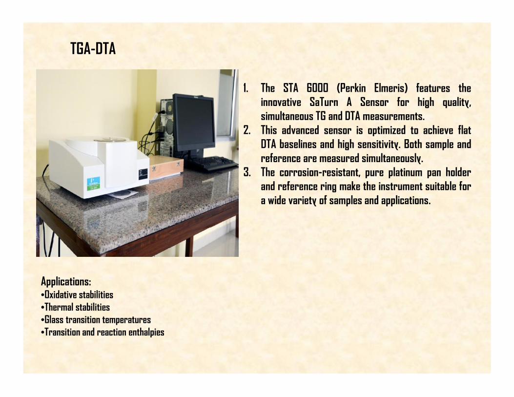
1. The STA 6000 (Perkin Elmeris) features theinnovative SaTurn A Sensor for high quality,simultaneous TG and DTA measurements.
2. This advanced sensor is optimized to achieve flatDTA baselines and high sensitivity. Both sample andreference are measured simultaneously.
3. The corrosion-resistant, pure platinum pan holderand reference ring make the instrument suitable fora wide variety of samples and applications.
Applications:•Oxidative stabilities•Thermal stabilities•Glass transition temperatures•Transition and reaction enthalpies
High Vacuum Thermal Coating
1. High Vacuum Thermal/ e-beam Coating Unit (ModelBC-300 HHV) is a versatile coating unit for thin filmapplications with facilities for evaporation, glowdischarge cleaning etc.
2. The system offers a variable source to targetdistance of 30cm-80cm & uniform deposition over 3cm diameter.
3. The temperature of the substrate can be variedfrom 27 0C to 550 0C possible deposition materialsare all semiconductors, oxides & metals.
1. Microwave reactors (CEM Discover) opens avenuesfor a wide range of conditions and variables to beinvestigated. The reactions can be run up to 300°Cand 300 psi in 10-mL to 80-mL sealed vessels.Additionally, open-vessel reactions can be run usingconventional round-bottom flasks (up to 125 mL)equipped with a reflux condenser.
Applications:•Opening of new reaction pathways•Increase in yields in difficult chemistries•Increase of purity profiles/selectivity in product mixtures•Decrease of reaction times from hours or days to minutes
Spin Coater
1. Spin Coating System (APEX) is an indispensable toolfor fabricating thin films on a suitable substrate with5000 .rpm
Applications:•Thin film coatings on semiconductors/ metals & glass•Casting of organic films•Micro circuiting etc
Chemical Vapour Deposition
1. Thermal chemical vapour deposition unit (TechnosInstruments) is an economical R&D system withuniform heating zone providing process solutionsfor production of single & multi walled carbonnanotube (SWCNT & MWCNT respectively) usingfixed bed method.
Applications:•CNT growth for various devices•Fludity•Carbon fiber and particles
Vacuum Impregnator
1. Cast n’ Vac 1000 (Buehler) evacuates entrapped airfrom specimens. Without the presence of air, themounting compound fills the specimen pores andeliminates gaps between the specimen and thecompound.
2. As a result, edge retention is enhanced and friablesamples are supported during grinding and polishing.
Applications:•Providing vacuum to eliminate gaps between specimens and compound
Semiconductor Device Parameter Analyzer
1. Semiconductor Device Analyzer ( Agilent B1500A) integratesmultiple measurement and analysis capabilities for accurateand quick device characterization into a single instrument.
2. It is the only parameter analyzer with the versatility toprovide both a wide range of device characterizationcapabilities along with uncompromised measurementreliability and repeatability.
3. It supports all aspects of measurement, from fundamentalcurrent-voltage (IV) and capacitance-voltage (CV)characterization up to state-of the art fast pulsed IV testing.
4. In addition, the B1500A’s ten-slot modular architectureallows you to add or upgrade measurement modules ifmeasurement needs change over time.
1. COMSOL Multiphysics is a finite element analysis, solver and Simulation software /FEASoftware package for various physics and engineering applications, especially coupled phenomena,or multiphysics.
1. COMSOL Multiphysics is a finite element analysis, solver and Simulation software /FEASoftware package for various physics and engineering applications, especially coupled phenomena,or multiphysics.
1. Integrated Circuit Characterization and Analysis Program (IC-CAP) is the industry standard for DC andRF semiconductor device modeling. IC-CAP extracts accurate compact models used in highspeed/digital, analog and power RF applications.
2. The most advanced semiconductor foundries and IDMs rely on IC-CAP for modeling silicon CMOS,Bipolar, compound gallium arsenide (GaAs), gallium nitride (GaN) and many other device technologies.IC-CAP is the most advanced, customizable modeling software and includes measurement, simulation,optimization and statistical analysis tools.
Applications•Open software architecture enables maximum accuracy and provides ultimate flexibility to create andautomate measurement, extraction and verification procedures•Turnkey extraction solutions for industry standard CMOS models, such as BSIM3/BSIM4, PSP and HiSIM,minimize the learning curve and maximize model accuracy•Most direct links to commercial simulators ensure consistency between extracted models and thesimulators used by circuit designers