Page 1
Natural Sciences Tripos Part IA
MATERIALS SCIENCEMATERIALS SCIENCE
Course A: Atomic Structure of Materials
Prof. Paul Midgley
Michaelmas Term 2013 14
Name............................. College..........................
Michaelmas Term 2013-14
IA
Page 2
Course A: Atomic Structure of Materials
AH1
MATERIALS SCIENCE
Course A: Atomic Structure of Materials
Paul Midgley
12 lectures
Student’s Edition
(There are some (deliberate) gaps in the handout – these will be filled
in during the lectures!)
Page 3
Course A: Atomic Structure of Materials AH2
Contents
Introduction 7
A. Crystals and Atomic Arrangements 12
A1. Historical introduction
A2. The packing atoms in 2D 15
A3. The packing of atoms in 3D 16
A4. Unit cells of the hcp and ccp structures 21
A5. Square layers of atoms 24
A6. Interstitial structures 26
B. 2D Patterns, Lattices and Symmetry 33
B1. 2D patterns and lattices 35
B2. Symmetry elements 38
B3. 2D lattices 41
B4. The 2D plane groups 44
C. Describing Crystals 45
C1. Indexing lattice directions (zone axes) 45
C2. The angles between lattice vectors (interzonal angles) 47
C3. Indexing lattice planes - Miller indices 48
C4. Miller indices and lattice directions in cubic crystals 51
C5. Interplanar spacings 53
C6. Weiss zone law 56
D. Lattices and Crystal Systems in 3D 58
E. Crystal Symmetry in 3D 62
E1. Centres of symmtery and roto-inversion axes 62
E2. Crystallographic point groups 66
E3. Crystal symmetry and properties 67
E4. Translational symmetry elements 69
E5. Space groups 71
F. Introduction to Diffraction 72
F1. Interference and diffraction 72
F2. Bragg’s law 76
F3. The intensities of Bragg reflections 79
G. The Reciprocal Lattice 88
Page 4
Course A: Atomic Structure of Materials
AH3
H. The Geometry of X-ray Diffraction 96
H1. The Ewald sphere 96
H2. Single crystal X-ray diffractometry 99
H3. X-ray powder diffractometry 101
H4. Neutron diffraction 103
I. Electron Microscopy and Diffraction 104
I1. Electron diffraction 104
I2. Microscopy and image formation 109
I3. Electron microscopy 114
Appendix 1. 2D plane groups 117
Appendix 2. Point groups 119
Appendix 3. Complex numbers 121
Appendix 4. Proof of Weiss Zone Law 123
Glossary of terms 124
Glossary of symbols 130
Page 5
Course A: Atomic Structure of Materials AH4
Recommended Text Books
No single textbook matches this course exactly, but reading parts of the
following will be helpful:
C. Hammond, The Basics of Crystallography and Diffraction, III
Ed, Oxford University Press, 2009
This is also available as an e-book, see:
http://www.msm.cam.ac.uk/library/ebooks_msm.php
A. Putnis, Introduction to Mineral Sciences, Cambridge University
Press, 1992
B.D Cullity, S.R Stock, Elements of X-Ray Diffraction, Prentice
Hall, 2001
D. McKie, C. McKie, Essentials of Crystallography, Blackwell
Scientific Publications, 1986
P. Goodhew, F.J. Humphreys and R. Beanland, Electron
Microscopy and Analysis 3rd Edition, Taylor and Francis 2001.
D. Williams and C.B. Carter, Transmission Electron Microscopy
Kluwer/Plenum Press, 1996 to 2004
Other books well worth looking at are:
Fundamentals of Materials Science and Engineering W.D. Callister
(Wiley)
The Structure of Materials S.M. Allen and E.C. Thomas (Wiley).
Page 6
Course A: Atomic Structure of Materials
AH5
Web Resources and Software The following location provides downloadable items relating to the
course (lecture handout, practicals, questions sheets, answers) as well as
links to material which may be of interest:
http://www.msm.cam.ac.uk/teaching/partIA.php
To accompany IA Materials there are complementary on-line Teaching
and Learning Packages within the DOITPOMS web site:
http://www.doitpoms.ac.uk/index.html
It should be available in your College computer centres and on many PCs
in the Department. The pages that are of particular use for this course are:
Diffraction and Imaging
Indexing Electron Diffraction Patterns
Optical Microscopy
Reciprocal Space
Transmission Electron Microscopy
X-ray Diffraction Techniques
Atomic Scale Structure of Materials
Crystallography
Lattice Planes and Miller Indices
The Stereographic Projection
There is also a great deal of useful web-based teaching at the MATTER
web site:
http://matter.org.uk/
Other Websites
Steffen Weber's homepage http://jcrystal.com/steffenweber/
Contains java-based applets that allow the structure of common polyhedra
and crystals to be explored.
Crystallography and Minerals Arranged by Crystal Form
http://webmineral.com/crystall.shtml
A library of 'crystal forms' - the shapes adopted by natural crystals.
Contains Java applets.
Page 7
Course A: Atomic Structure of Materials AH6
EPFL host a useful web site on many aspects of crystallography:
http://escher.epfl.ch/eCrystallography/
Crystal Maker
http://www.crystalmaker.com/
This is excellent software for visualizing crystal structures and for
simulations of diffraction patterns. Copies to use are available on many
Department PCs. The Department has a site licence.
E-mail address
Feedback on any aspect of the 1A Materials Science course may be
directed to: [email protected]
Page 8
Course A: Atomic Structure of Materials
AH7
Introduction
Materials science plays a key role in almost all aspects of modern life and
in the technologies and equipment we rely upon as a matter of routine.
There are many examples to choose from but one that usefully illustrates
this is the Apple iPhone. Almost all the components have relied upon
advances in materials science and the work of materials scientists!
Consider some of the materials involved and their application:
Display. This relies upon the combination of a liquid crystal display and
a touch screen for communication with the device. You will hear more
about liquid crystals later in the year. The touch screen is made from a
conductive but transparent material, indium tin oxide, a ceramic
conductor.
ICs At the heart of the iPhone are a number of integrated circuits (ICs)
built upon billions of individual transistors, all of which rely on precise
control of the semiconductor material, silicon, to which has been added
dopant atoms to change the silicon’s electronic properties. Adding just a
few dopant atoms per million silicon atoms can change the conductivity
many orders of magnitude!
Interconnects Interconnects that provide the links between components
are now made of copper, not aluminium, for higher speed and efficiency.
Battery The battery is a modern Li-ion battery where the atomic structure
of the electrodes is carefully controlled to enable the diffusion of the Li
ions.
Page 9
Course A: Atomic Structure of Materials AH8
Wireless Microwave circuits need capacitors which are ceramic
insulators whose structure and composition is carefully controlled to
optimise the capacitance.
Headphones. Most headphones use modern magnetic materials whose
structure and composition has been developed to produce very strong
permanent magnets. This is part of a transducer that turns electrical
signals into sound.
With the exception of the LCD, all these materials are solid materials.
Classification and Terminology
Traditionally states of matter were classed into 3 ‘classical’ groups:
Gases Liquids Solids
Although gases and liquids are of course important in the understanding
of materials, in Course A we will concentrate solely on solids and in
particular on crystalline solids.
Nowadays these 3 traditional groups have been joined by other states of
matter including for example liquid crystals which lie at the boundary
between liquids and solids and will be discussed in other parts of the
Materials course.
Solid materials can be classified into many different types and in many
different ways depending on whether you want to stress, for example,
their structure or their mechanical or electrical properties.
Traditionally we might talk about
Metals Ceramics Polymers*
(*You will investigate the mechanical properties of a polymer in AP0)
which again are very broad descriptions and with lots of overlap, for
example many ceramics are good conductors and thus in some sense
could be called ‘metallic’.
Page 10
Course A: Atomic Structure of Materials
AH9
We also talk about groups of materials stressing for example their
electrical and magnetic properties, so we talk about
Semiconductors
Superconductors
Hard and Soft Magnetic Materials
Ferroelectric Materials
…and so on.
In addition we study solids that are crystalline (that have a crystal
structure) and non-crystalline.
A crystalline solid is one in which the atoms are arranged in a periodic
fashion – we talk about ‘long-range order’.
A non-crystalline material is non-periodic it does not have long-range
order but can have ‘short range order’ where the local arrangement of
atoms (and the local bonding) is approximately the same as in a crystal.
crystalline non-crystalline
Page 11
Course A: Atomic Structure of Materials AH10
Importance of Atomic Structure
What is common to all materials is that they are composed of atoms.
The properties (whether mechanical, electrical, chemical etc) of all solid
materials are dependent upon the relative positions of the atoms in the
solid (in other words the atomic structure of the material) and their
mutual interaction i.e. the nature of the bonding (whether e.g. covalent,
ionic, metallic, van der Waals).
There are examples of where the atom-atom interactions is strongly
reflected in the atomic structure. An example is diamond. Here the
carbon-carbon interactions lead to a very directional covalent bond called
a sp3 bond which has tetrahedral symmetry – this leads to an open
structure as shown below.
Of course carbon can also take the form of graphite. Here the carbon
atoms are arranged in a rather different structure and graphite has very
different properties to diamond!
In other solid systems (for example many of the metallic elements) the
atomic structure is dictated by how well we can ‘pack’ the atoms into 3D
space – ‘packing efficiency’ – this leads to dense close-packed structures
as we will also discuss very shortly.
So it is vital that to understand the properties of material, and to improve
those properties for example by adding or removing atoms, we need to
know the material’s atomic structure.
Page 12
Course A: Atomic Structure of Materials
AH11
As Richard Feynman said:
‘It would be very easy to make an analysis of any complicated chemical
substance; all one would have to do would be to look at it and see where
the atoms are…’
taken from ‘There’s Plenty of Room at the Bottom’, Richard Feynman
lecture, APS meeting at Caltech, 1959
Richard Feynman
So let’s start understanding materials by understanding their atomic
structure….
Page 13
Course A: Atomic Structure of Materials AH12
A. Crystals and Atomic Arrangements
A1. Historical Introduction
There is a great deal of evidence in nature that many materials have some
kind of internal order, evidence of a pattern or arrangement of underlying
building blocks.
Consider the following examples:
An array of micrographs showing the hexagonal symmetry of ice crystals
(snowflakes)
Natural quartz crystals (left) and the facetted surface of a fractured iron-
aluminium single crystal (right)
Page 14
Course A: Atomic Structure of Materials
AH13
We now know that all materials are composed of atoms and it is the
arrangement of the atoms that leads to the external shapes we see in the
figures above.
Although Kepler (1611) was the first to discuss the 6-fold symmetry of
the snowflake, it was Hooke (1665) who was the first to consider the
structure of ‘crystalline’ materials in his seminal book ‘Micrographia’ –
pictures below reproduced from his book:
Page 15
Course A: Atomic Structure of Materials AH14
Haüy (1784) showed how different forms (we now say ‘habits’) of dog-
tooth spar (calcite) can be described by packing together small rhombs
which he called ‘molécules intégrantes’.
With our current knowledge we realise that Hooke’s description was in
essence the packing of atoms to form a crystal and Hauy was describing
the periodic array of ‘unit cells’ – more on this later…
Page 16
Course A: Atomic Structure of Materials
AH15
A2. Packing Atoms in 2D
Consider again Hooke’s picture. Apart from ‘L’, the atoms are packed in
a 2D close-packed hexagonal arrangement. In L, the atoms are in a
square arrangement. Note there are larger gaps (interstices) in the square
arrangement.
The efficiency of this 2D packing is easily calculated by considering the
filling of the 2D plane with circles:
Square Packing
Hexagonal Packing – see question sheet.
square of side a
circle diameter a
a
Page 17
Course A: Atomic Structure of Materials AH16
A3. Packing Atoms in 3D
Let’s extend this picture to 3D and consider the packing of spheres (to
represent atoms).
Consider again the close-packed hexagonal arrangement in one layer:
If we extend to 3D, the next layer of atoms could be placed directly above,
i.e. the centre of the atoms in the next layer are also at A.
The resultant crystal structure is called the simple hexagonal structure.
(Note what defines a crystal to be hexagonal we will see later).
However, no examples of elements with this structure exist in nature
because the atoms can ‘slip’ into the ‘hollows’ or interstices between the
atoms. This creates a more efficient packing of 3D space and is
energetically more stable – for more on energy considerations, see course
C.
So now consider the next layer of atoms centred at the interstice B:
A A A A
A A A A
A A A A
a
120
Page 18
Course A: Atomic Structure of Materials
AH17
If the 3rd
layer atoms ‘slip’ into the interstices of the 2nd
layer then they
may end up directly above the atoms of the 1st layer.
The stacking sequence is then ABAB and this is called the hexagonal
close-packed (hcp) structure. Seen from the side:
c
a
d
d
A A A A
A A A A
A A A A
B B B B
B B B B
Page 19
Course A: Atomic Structure of Materials AH18
In the ideal hcp structure, as shown, then ad3
2 (see question sheet!)
Let’s define d as the spacing between the layers (or ‘planes’) of atoms,
then
aadc 633.13
222
Interatomic forces in real crystals cause deviations from the ideal c/a ratio
but metals such as Be, Mg and Co have hcp structures with c/a ratio close
to the ideal.
Metal c/a ratio
Mg 1.623
Co 1.622
Be 1.567
But there is an alternative interstice in the 1st layer – let’s label it as C.
Atoms in the 3rd
layer could be placed above C and not A.
Then the sequence would be ABCABC and the resultant structure is
called the cubic close-packed (ccp) structure. What defines a ‘cubic’
crystal, we will see later.
Why do we say the structure is cubic? It is because of the choice of unit
cell and its symmetry – see below.
Q
P
A A
A
A
B
C
A
A
B
B
B B B
C
Page 20
Course A: Atomic Structure of Materials
AH19
Seen from the side, looking parallel to P and Q:
If we rotate the crystal 45 about the axis as shown on the right above,
then we see the following:
and the cubic symmetry of the crystal structure starts to become more
obvious.
Many elements have the ccp structure including Cu, Ni and Al.
Notes:
1. Some elements have a ‘mixture’ of ccp and hcp stacking.
For example: Nd and Sm have ….ABACABAC….
2. It is also possible to have ‘mistakes’ in the stacking sequence – known
as stacking faults.
A
B
C
A
direction P direction Q
Page 21
Course A: Atomic Structure of Materials AH20
For example for hcp:
….ABABABABABCBCBCBCBCBC….
Stacking faults can be seen directly in the transmission electron
microscope:
High-resolution electron microscope image showing the location of a
stacking fault in a core-multishell ZnS nanowire
‘ccp’
fault
}
Page 22
Course A: Atomic Structure of Materials
AH21
A4. Unit Cells of the hcp and ccp Structures
We need to find a way to represent the hcp and ccp structures with fewest
number of atoms that still show the essential structure and symmetry –
these are the unit cells.
Simple Hexagonal
Hexagonal Close-Packed (hcp)
120
a
c
a
Unit Cell Angles = 90, 120
plan view
plan view
a a
c
a
a 120
ideal c/a =1
a
a
Unit Cell Angles = 90, 120
½
Page 23
Course A: Atomic Structure of Materials AH22
Cubic Close-Packed (ccp)
Packing Efficiency of ccp and hcp structures:
Assume atoms are touching in the close-packed plane (orange triangle),
along the diagonal of the faces of the unit cell (the ‘face diagonal’):
a a
a Unit Cell Angles = 90
Page 24
Course A: Atomic Structure of Materials
AH23
Page 25
Course A: Atomic Structure of Materials AH24
A5. Square Layers of Atoms
Consider a single layer of atoms arranged in a square lattice:
The next layer could be placed directly on top. This then forms the
simple cubic structure. An example is -polonium.
Or the next layer could ‘slip’ into the interstices, such as the one marked
‘X’ above.
X
a
a
a
Unit Cell Angles = 90
Page 26
Course A: Atomic Structure of Materials
AH25
The 3rd
layer can then placed above the 1st layer:
Here if we consider the unit cell as shown then the atoms of the 2nd
layer
are in the centre of the cube – we call this structure body-centred cubic
(bcc).
Many metals take this structure, e.g. Cr, Mo, Ti (high temperature form),
Fe (low temperature form).
In the bcc structure the atoms are most closely packed in the diagonal
plane with atoms touching only along the body diagonal.
Packing Efficiency of bcc – see question sheet!
a
a
a
Unit Cell Angles =
90
Page 27
Course A: Atomic Structure of Materials AH26
A6. Interstitial Structures
We’ve considered the packing of one size of atom (sphere) but we can
also use these ideas to describe the structure of compounds with two or
more elements.
This is especially useful for compounds with dissimilar atoms sizes where
‘small’ atoms or ions (often cations) fit into the interstices between
‘large’ atoms or ions (often anions). As we will see there are a number of
possible interstices to choose – which one would the atom, or ion, fit
best? Need to invoke:
Goldschmidt’s Packing principle:
The number of anions surrounding a cation tends to be as large as
possible, subject to the condition that all anions touch the cation.
cation
anion
‘ideal’ unstable
stable
Page 28
Course A: Atomic Structure of Materials
AH27
Consider again the ccp structure (for clarity only some atoms are shown):
It is possible to place an atom at an interstitial site (coloured blue) which
is at the centre of the tetrahedron formed by the 4 (black) atoms shown.
The 4 atoms surround or co-ordinate the smaller interstitial atom at a
tetrahedral interstice.
What size of atom can be accommodated in the tetrahedral interstice? The
limiting case, according to Goldschmidt’s Principle (the geometrically
‘ideal’ size) would be when the large atoms and the interstitial atom all
just touch. Therefore it depends on the ratio of the size of the two atoms:
Consider large atoms (call them A atoms) have radius Ar and interstitial
atoms have radius Xr .
For ccp structures, the A atoms touch along the face diagonal.
¼, ¾
interstitial site
plan view ½
½
Page 29
Course A: Atomic Structure of Materials AH28
For the ideal case, atoms A and X touch along the body diagonal:
Consider another possible interstitial site:
Here an interstitial atom can be placed at the centre of an octahedron of 6
atoms, hence the name octahedral interstice and the interstitial atom is
6-fold co-ordinated.
The space available in the octahedral interstitial site is larger and so can
accommodate an atom of larger radius. What is the ‘ideal’ radius ratio?
See question sheet!
Note: Of course the interstitial spaces available in hcp are the same as ccp
– the two structures differ only by a stacking sequence.
interstitial site
Page 30
Course A: Atomic Structure of Materials
AH29
The table below gives the relation between radius ratio and co-ordination
number:
Radius ratio
rx / rA
Coordination
number
Type
<0.155 2 Linear
0.155-0.225 3 Triangular
0.225-0.414 4 Tetrahedral
0.414-0.732 6 Octahedral
0.732-1.000 8 Cubic
1.000 12 Cuboctahedral
(Close packed)
So for example if a radius ratio was calculated to be, say 0.5 then the
interstitial atom would be accomodated in an octahedral site. However, if
the ratio decreased to say 0.4 the atom would be in a tetrahdral site.
Notice how the co-ordination number increases as the cation and anion
radii become similar.
Consider now the simple cubic structure:
The interstitial atom is placed at the centre of the cube surrounded by 8
atoms and the site is called the cubic interstitial site.
interstitial site
Page 31
Course A: Atomic Structure of Materials AH30
An example of this is CsCl with a smaller Cs+ ion (green) surrounded by
larger Cl- ions (purple).
Similar interstitial sites are present in bcc crystals but these are ‘distorted’
octahedral and tetrahedral interstices in that some A atoms will be closer
to the interstitial atom than others in the octahedron / tetrahedron. In
terms of calculating how well the interstitial atom will fit, it is of course
the distance to the nearest A atom that matters!
In the figure below, as an example, we show the ‘distorted’ octahedral
sites in bcc.
interstitial site
Page 32
Course A: Atomic Structure of Materials
AH31
Other examples of interstitial compounds are metal hydrides, borides and
nitrides. In these cases the ‘large’ atoms are the metal atoms:
TiN
Ti ccp structure
N in octahedral interstices
6-fold co-ordination of Ti
around N
6-fold co-ordination of N
around Ti.
(isomorphous with NaCl)
TiH2
Ti ccp structure
H occupy ALL tetrahedral
interstices
4-fold co-ordination of Ti
around H
8-fold co-ordination of H
around Ti.
(isomorphous with CaF2)
TiH
Ti ccp structure
H occupy half the
tetrahedral interstices
4-fold co-ordination of Ti
around H
4-fold co-ordination of H
around Ti
(isomorphous with ZnS)
Page 33
Course A: Atomic Structure of Materials AH32
Representing Crystal Bonding with Co-ordination Polyhedra:
Crystal structures can be represented using ball and stick models or with
co-ordination polyhedra. Here we use BaTiO3 as an example of both:
Page 34
Course A: Atomic Structure of Materials
AH33
B. 2D Patterns, Lattices and Symmetry
In section A we took a pragmatic approach to building up the structure of
simple crystalline materials using the close packing of atoms.
To explore more complicated structures, and to describe the structures of
crystals in a more systematic and rigorous way, we need to adopt a
different approach.
By having a more rigorous framework to describe crystals we’ll be able
to interpret experimental diffraction patterns and determine crystal
structures, just as Crick and Watson did in 1953!
The famous ‘Photo 51’: X-ray diffraction pattern of sodium salt of DNA.
B configuration. This pattern will be studied further in Question Sheet 3!
Page 35
Course A: Atomic Structure of Materials AH34
Page 36
Course A: Atomic Structure of Materials
AH35
B1. 2D Patterns and Lattices
We start in 2D and consider 2D patterns and lattices. Examples of such
patterns can be found for example on the tiled walls of the Alhambra
Palace in Granada:
The artist M.C. Escher was instrumental in bringing the geometry of 2D
tiling to a wider audience (see also Question Sheet 2!):
Page 37
Course A: Atomic Structure of Materials AH36
Consider a regular 2D pattern composed of the letter ‘R’ repeated
indefinitely.
The repeating ‘unit of pattern’ is called the motif. In a crystal, the motif is
composed of atoms.
The motifs can be considered to be situated at or near the intersections of
an (imaginary) grid.
The grid is called the lattice and the intersections are called lattice points.
Sometimes, it is said that ‘structure = lattice + motif’. What this really
means is that all crystal structures can be built up by placing a motif of
atoms at every lattice point.
R R R R
R R R R
R R R R
R R R R
R R R R
R R R R
unit cell
R R R R
R R R R
R R R R
Page 38
Course A: Atomic Structure of Materials
AH37
The lattice in 2D is completely specified by a statement of the repeat
lengths a and b parallel to its x-axis and y-axis and its interaxial angle γ.
In principle, there are an infinite number of ways of drawing the lattice
but convention is to choose a lattice to give a unit cell with angles closest
to 90.
Each motif is identical and for an infinitely extended pattern, the
environment (i.e. the spatial distribution of the surrounding motifs and
their orientation) around each motif is identical. Leads to….
Definition of a Lattice
A lattice is an infinite array of points repeated periodically throughout
space. The view from each lattice point is the same as from any other.
γ a
b
x
y
Page 39
Course A: Atomic Structure of Materials AH38
B2. Symmetry Elements
Consider:
Here the unit cell and lattice is as before but now the motif is
Clearly there’s an internal rotational symmetry in the motif. A rotation
of 180 (2-fold) about an axis through the lattice point marked.
The 2-fold rotation axis is called a DIAD and is represented by fi. Thus:
Notice that additional diads are now generated in the 2D structure, at the
mid-points between neighbouring lattice points and at the centre of the
unit cell.
Other rotation axes are possible:
3-fold: TRIAD 4-fold: TETRAD 6-fold: HEXAD
In addition to rotational symmetry, it is also possible to have mirror
symmetry as part of the motif:
R RR R
R RR R
R RR R RR RR
RR RR
RR RR
RR
RR.
RRfi
4 6 fl
R
m
Page 40
Course A: Atomic Structure of Materials
AH39
Or a combination of rotation axes and mirrors. This leads to the 10 2D
crystallographic or plane point groups.
Definitions
The symmetry elements (or operators) of a finite body must pass through
a point, taken as the centre of the body: such a group (or combination) of
symmetry elements is known as a point group.
The 10 2D crystallographic or plane point groups are illustrated below
(taken from Hammond’s book):
1
m
2mm
2
3
3m
4
4mm
6
6mm
Page 41
Course A: Atomic Structure of Materials AH40
Aside:
Why not point groups with 5-fold rotation axes, or 7-fold, etc? Definitely
possible to have for example 5-fold point group! For example the motif
on the flag of Hong Kong:
However, only these 10 point groups can occur in regular repeating 2D
patterns. Patterns with 5-fold symmetry are non-repeating, non-periodic.
If you try to fit pentagons together you get gaps! The overall pattern does
not have 5-fold symmetry.
Page 42
Course A: Atomic Structure of Materials
AH41
B3. 2D Lattices
The need for periodic tiling of the 2D surface limits the number of
possible 2D lattices to just 5:
p -‘primitive’ 2D lattice – only one lattice point per unit cell
c -‘centred’ 2D lattice – two lattice points per unit cell
Why not just choose a primitive cell for rectangular c?
Indeed we can! But it does not reflect the full symmetry of the lattice –
we choose a larger unit cell and a centred lattice because the axes joining
the sides are at 90.
a
b
a
b b
a
a
a a
a
120
oblique p rectangular p rectangular c
square p hexagonal p
Page 43
Course A: Atomic Structure of Materials AH42
We are almost ready to combine the motif and the lattice but we first need
to consider one further symmetry element called a glide line in 2D (glide
plane in 3D).
Consider a rectangular p lattice:
R
R R
R
R R
m m m
Notice an extra mirror
is generated
‘automatically’.
lattice points
motif
R
R R
R
R R
g g g
Glide Lines
An extra glide line also
generated
R
R
R
The Action of a Glide:
glide reflect about line/plane
and translate by ½ lattice
spacing
Page 44
Course A: Atomic Structure of Materials
AH43
‘Macroscopic’ example of a glide line (footprints on a beach at St Kitts!):
g
Page 45
Course A: Atomic Structure of Materials AH44
B4. The 2D Plane Groups
So we can now put together the 5 possible 2D lattices with the 10
possible crystallographic 2D point groups to give all the possible 2D
plane groups – there are 17 in total.
These are shown in Appendix 1.
Consider just one example here. We saw from before:
From Appendix 1:
Some symmetry elements (glides, diads) are generated automatically. For
example extra glide lines in p4mm, extra diads in p2.
R RR R
R RR R
R RR R RR RR
RR RR
RR RR
fi
fi fi
fi fi
fi
fi
fi
fi
Page 46
Course A: Atomic Structure of Materials
AH45
C. Describing Crystals
Before we continue with our analysis of crystallographic symmetry in 3D,
we need to explore a convenient system to describe directions and planes
in crystals.
C1. Indexing Lattice Directions (Zone Axes)
Consider a general 3D lattice with lattice points and unit cell as shown:
The unit cell has unit cell edge vectors sometimes called basis vectors:
a, b, c (which are not necessarily orthogonal or equal).
We want to write the direction OL using convenient nomenclature or
index.
(i) Co-ordinates of P are ½,0,1
(ii) Express as a ratio of whole numbers (multiply by 2 in this case) and
put in square brackets, i.e. [102]
(iii) Thus [102] is the direction symbol for OL.
Consider now SN, shift origin to S (or consider OM which is parallel to
SN) and proceed as before to find SN = 011 which we say as ‘one bar-
one oh’.
a
b
x
y
c
z
L
P
N
M
O
Q S
Page 47
Course A: Atomic Structure of Materials AH46
Directions can be written in terms of the basis vectors:
r102 = 1a + 0b + 2c
Thus in general for a direction [uvw]:
ruvw = ua + vb + wc
Notes
a, b, c are thus [100], [010] and [001].
When using crystallographic axes, we often talk about the a, b, c axes
rather than x, y, z axes.
Page 48
Course A: Atomic Structure of Materials
AH47
C2. Angles Between Lattice Vectors (Interzonal Angles)
The angle between two vectors p and q is given by the dot, or scalar,
product:
p.q = pq cos where p = p and q = q
Therefore
pq
qp.cos 1
Consider a unit cell with a b c, = = =90
p = [u1 v1 w1] q = [u2 v2 w2]
Consider general vector [uvw], we can write:
[uvw] = ua + vb + wc
= uai + vbj + wck
where a = a, b = b and c = c
i = unit vector in direction a
j = unit vector in direction b
k = unit vector in direction c
Therefore 22
2
22
2
22
2
22
1
22
1
22
1
2
21
2
21
2
21coscwbvaucwbvau
cwwbvvauu
a
b
x
y c
z
O
q
p
Page 49
Course A: Atomic Structure of Materials AH48
C3. Indexing Lattice Planes – Miller Indices
A lattice plane is a plane which passes through any three lattice points
which are not in a straight line.
A set of parallel lattice planes is characterised by its Miller indices (hkl).
Consider again a general 3D lattice:
The routine for indexing the plane EMS is as follows:
(i) write down the intercepts of the plane on the axes of the unit cell or
unit cell vectors a, b, c.
i.e. ½a, 1b, 1c
expressed as fractions of the cell edge length this is ½, 1, 1
(ii) Take the reciprocal of these fractions and put the whole numbers into
round brackets:
This gives (211) - this is the Miller index of plane EMS
x
y
z
O
S
E
M
Page 50
Course A: Atomic Structure of Materials
AH49
Now consider the following set of planes:
What’s the index of this set of planes?
Easiest way to tackle this is to move the origin to a different lattice point
– always allowed to do this! Let’s move the origin to O keeping the
direction of the axes the same.
Intercepts (relative to O) for the first plane seen in the series are at:
-1, ½, -½
Therefore the plane is 221
In general a plane (hkl) will intercept the x-axis at a/h, the y-axis at b/k
and the z-axis at c/l
x
y
z
O
O
x
y
z
O
b/k
a/h
c/l
Page 51
Course A: Atomic Structure of Materials AH50
But remember there are a set of parallel planes (hkl), so the first plane
intercepts the x-axis at a/h, the second at 2a/h, the third at 3a/h, and so on.
Remember also that the origin can be moved and so (hkl) is equivalent to
( lkh ).
Page 52
Course A: Atomic Structure of Materials
AH51
C4. Miller Indices and Lattice Directions in Cubic Crystals
The positive and negative directions of the crystal axes vectors
a, b, c
can be expressed as
[100], [ 001 ], [010], [ 010 ], [001], [ 100 ]
In a cubic crystal the axes are crystallographically equivalent and
interchangeable and may be expressed collectively as <100>, implying all
6 variants of 1,0,0.
In fact we can do this for any direction in the cubic system, so for a
general direction <uvw> there are 48 (24 pairs) variants. For example
consider for yourself <123>.
A similar concept can be applied to Miller indices of crystal planes. The 6
faces of a cube (with the origin at the centre) are:
(100), ( 001 ), (010), ( 010 ), (001), ( 100 )
These are expressed collectively as {100}. Such a group of planes is
sometimes known as a form.
For a general plane {hkl} in the cubic system, there are 48 (24 pairs)
variants. This number is sometimes known as the multiplicity and given
the symbol mhkl. It is an important quantity when interpreting the
intensities of powder x-ray diffraction patterns – see later.
So for example the multiplicity of the {100} planes is 6, for the {111}
planes, it is 8, and so on.
shaded planes are
(010), ( 010 ).
z
x
y
Page 53
Course A: Atomic Structure of Materials AH52
For a cubic system, the directions are perpendicular to planes with the
same numerical indices. For example
[110] is perpendicular to (110);
[123] is perpendicular to (123).
But this is not true in general! See below:
(110) (110)
[110] [110]
CUBIC NON-CUBIC
x
y
x
y
Page 54
Course A: Atomic Structure of Materials
AH53
C5. Interplanar Spacings
Consider the following planes:
Looking in plan view:
In general, consider a plane (hkl):
x
y
z
O
A
B
x
y
z
O C
D
(110) (220)
C
D
A
B
d110 d220
x
y
z
O
b/k
a/h
c/l
N
A (hkl)
Page 55
Course A: Atomic Structure of Materials AH54
There is of course a parallel plane (not shown) passing through the origin,
O, and so the interplanar spacing is given by the length of the normal to
the (hkl) plane, ON.
Angle AON = (angle between normal and x-axis)
Angle
Define: as the angle between ON and the y-axis
as the angle between ON and the z-axis
Therefore by comparing to above, we can write:
hkldb
k
cos and hkld
c
l
cos
For orthogonal axes, using Pythagoras’ theorem,
1coscoscos 222
we can write that 12
2
2
2
2
2
hklhklhkl d
c
ld
b
kd
a
h
and
222
2
1
c
l
b
k
a
h
dhkl
For cubic crystals, a = b = c
and a
lkh
dhkl
2221 or
222 lkh
adhkl
.
Page 56
Course A: Atomic Structure of Materials
AH55
Measuring Interplanar Spacings with X-Rays
Recall the x-ray photograph of DNA shown on AH33 (central part
reproduced below):
The x-ray diffraction pattern shows a series of spots (or ‘reflections’)
whose spacing depends upon the interplanar distances, d, in the DNA
crystal; the relationship is given by Bragg’s Law (known also as the
‘Bragg equation’):
λ = 2d sin θ
where is the x-ray wavelength and θ is known as the Bragg angle, as
shown below
You need Bragg’s Law for practical AP2. The derivation of Bragg’s Law
will be given later – see AH76.
θ 2θ
spots
x-ray
crystal
spots
Page 57
Course A: Atomic Structure of Materials AH56
C6. Weiss Zone Law
We said before that a lattice direction is sometimes called a zone axis.
Why? What’s a zone?
A zone maybe defined as a ‘set of faces or planes in a crystal whose
intersections are all parallel’.
The common direction of the intersections is called the zone axis.
An illustration of this:
All intersections of planes (e.g. AB) are parallel to the z-axis. Thus the
planes belong to a zone whose zone axis is parallel to z.
The Weiss Zone Law
If a lattice vector rUVW, or simply [UVW], is contained in a plane of the set
(hkl), there is a relationship that links the lattice vector to the lattice
planes:
hU + kV + lW = 0
Note: Proof of the Weiss Zone Law given in Appendix 4.
A
B
z
[UVW]
(hkl)
Page 58
Course A: Atomic Structure of Materials
AH57
In general we may wish to find the direction vector [UVW] which is
common to the planes (h1k1l1) and (h2k2l2). We need to solve 2
simultaneous equations:
h1U + k1V + l1W = 0
h2U + k2V + l2W = 0
Solutions are:
U= k1l2 - l1k2
V= l1h2 – l2h1
W= h1k2 – h2k1
Page 59
Course A: Atomic Structure of Materials AH58
D. Lattices and Crystal Systems in 3D
We can now continue with our exploration of crystals in 3D armed with a
method to describe directions and planes.
Recall that we had 5 possible lattices in 2D. Taking one of those lattices
and stacking ‘layers’ on top of each other it is possible to build up all the
possible 3D lattices.
Doing this we find that there are 14 crystallographically distinct 3D space
lattices, called Bravais lattices.
The unit cells of the Bravais lattices are shown below, grouped into the 7
distinct crystal systems (or crystal classes).
Note we have primitive (P), body-centred (I), face-centred (F) and
base-centred (C) lattices. There is also a rhombohedral (R) lattice.
Page 60
Course A: Atomic Structure of Materials
AH59
Crystal System Defining Symmetry
(rotation or
inversion)
Conventional Unit
Cell
Conventional
Lattice
Types
Cubic 4 triads a = b = c
α = β = γ = 90° P, I, F
Hexagonal 1 hexad a = b ≠ c
α = β = 90°, γ = 120° P
Trigonal 1 triad a = b ≠ c
α = β = 90°, γ = 120° P, R
Tetragonal 1 tetrad a = b ≠ c
α = β = γ = 90° P, I
Orthorhombic 3 diads a ≠ b ≠ c
α = β = γ = 90° P, C, I, F
Monoclinic 1 diad a ≠ b ≠ c
α = γ = 90°, β ≥ 90° P, C
Triclinic - a ≠ b ≠ c
α ≠ β ≠ γ
P
The different shapes and sizes of these cells may be described in terms of
three cell edge lengths a, b, c or lattice vectors a, b, c, and the angles
between them , , .
Note, by convention: is the angle between b and c
is the angle between a and c
is the angle between a and b
But what defines something as being say‘cubic’, or ‘tetragonal’. It is not
the shape of the unit cell but the symmetry of the crystal.
For a crystal to belong to a particular system it must have a characteristic
(minimum) symmetry. For example
Cubic four 3-fold axes (triads) parallel to the <111> axes
Tetragonal one 4-fold axis (tetrad) parallel to the c-axis, the [001] axis.
Of course the empty lattice can have a higher symmetry than the crystal –
it depends on the position of atoms in the motif. For example there are
cubic crystals without 4-fold symmetry but whose unit cell has
orthogonal sides of equal length (i.e. a cube).
Page 61
Course A: Atomic Structure of Materials AH60
Centred Lattices
We saw in 2D the possibility of a centred lattice. In 3D there are also
centred lattices as well as the primitive lattice (P):
P lattice primitive lattice 1 lattice points / unit cell
I lattice body-centred lattice 2 lattice points / unit cell
F lattice face-centred lattice 4 lattice points / unit cell
C lattice base-centred lattice 2 lattice points / unit cell
(The last is called a C-centred lattice because the extra lattice point is in
the a-b face. It is possible to have A-centred and B-centred lattices but
these are non-conventional.)
We can always construct a primitive cell from the centred lattice. For
example consider below (a) the cubic I and (b) cubic F lattices:
However, as in 2D, these 3D primitive cells are not often used because:
(i) The inter-axial angles are not the convenient 90(i.e. they are not
orthogonal)
(ii) They do not reveal very clearly the cubic symmetry of the cubic I or
cubic F lattice.
Page 62
Course A: Atomic Structure of Materials
AH61
Close Packed Structures Revisited
The ccp structure has a cubic F lattice with one atom in the motif at 0,0,0.
The bcc structure has a cubic I lattice with one atom in the motif at 0,0,0.
The hcp structure has a hexagonal P lattice with two atoms in the motif at
0,0,0 and 2/3,
1/3,
1/2 .
Trigonal System
Some crystals with a hexagonal lattice (e.g. quartz) do not show
hexagonal symmetry (i.e. they do not have 6-fold rotational symmetry)
but have only 3-fold symmetry. As such, these crystals must be assigned
to the trigonal system.
Hence the trigonal system includes crystals with both hexagonal and
rhombohedral Bravais lattices.
-quartz (SiO2)
Page 63
Course A: Atomic Structure of Materials AH62
E. Crystal Symmetry in 3D
In 2D we found that by combining symmetry elements we could
determine 10 distinct crystallographic point groups.
In 3D we find that there are 32 distinct crystallographic point groups.
However to describe these we need to discuss two other symmetry
elements that exist only in 3D (not in 2D).
E1. Centres of Symmtery and Roto-Inversion Axes
If a crystal possesses a centre of symmetry, then any line passing
through the centre of the crystal connects equivalent faces, or atoms, or
molecules.
In other words, if an atom is located in the crystal at (x, y, z) then the
same atom must be located at (-x, -y, -z).
The origin O is called a centre of symmetry (or inversion centre) and a
crystal possessing a centre of symmetry is said to be centrosymmetric.
If a crystal does not posess a centre of symmetry, then it is said to be non-
centrosymmetric.
Consider how a centre of symmetry operates on a more complex object:
r
-r
r = (x, y, z)
O
A
B
C
D
A’ B’
C’
D’
Page 64
Course A: Atomic Structure of Materials
AH63
An everyday example of a centre of symmetry (inversion centre) is seen
in the figure below (c.f. with the mirror):
Consider again the previous figure, we can imagine the atoms at r
sitting on the surface of a sphere of radius r and the centre of symmetry
then being at the centre of the sphere.
Thus the stereographic projection shown above represents a centre of
symmetry (inversion centre).
It is given the symbol 1 and is marked on the stereographic projection as
a small circle
NOTE: In this course we use the stereographic projection only as a
pictorial device. However, it can be used quantitatively, for interest only
see: http://www.doitpoms.ac.uk/tlplib/stereographic/index.php
+r
-r
N
S
Stereographic Projection
Project object in northern hemisphere as
Project object in southern hemisphere as
inversion centre mirror
Page 65
Course A: Atomic Structure of Materials AH64
Can we combine centres of symmetry with rotation axes? Yes! They are
called roto-inversion axes.
For example using our stereographic projection we can first represent a 4-
fold axis (with the rotation axis pointing up):
Now combine this 4-fold rotation axis with an inversion centre to produce
a 4-fold roto-inversion axis. This is given the symbol 4 and the operation
is:
(i) rotate by 90 (i.e. 360/4)
(ii) invert through the centre
As before the roto-inversion axis is pointing up.
We can also have 3 and 6 symmetry axes.
What about 2 ? It is a horizontal mirror! Therefore 2 m .
90
4
≤
Notice that contained within the 4
symmetry element is a 2-fold rotation axis.
Hence the symbol is ≤ showing the
‘automatic’ presence of fi.
− bold to indicate a horizontal mirror
Page 66
Course A: Atomic Structure of Materials
AH65
So actually we can say also that a centre of symmetry is also a roto-
inversion axis 1 where the operation is to rotate by 360/1 and invert
through the centre.
Examples of roto-inversion axes
≤ `
3 4
Page 67
Course A: Atomic Structure of Materials AH66
E2. Crystallographic Point Groups
(Note: This section is for background only – non-examinable.)
Just as we did in 2D, we can combine symmetry elements to establish all
the possible crystallographic point groups.
In Appendix 2, we list all the 32 possible crystallographic point groups
showing the international symbol and a representative stereographic
projection.
As an example consider the tetragonal point group m24 :
‘ 4 ’ indicates a 4 roto-inversion axis parallel to the tetragonal c-axis
shown pointing up from the page.
‘2’ indicates a 2-fold axis (diad) perpendicular to the 4 axis (i.e. parallel
to both the a-axis and b-axis.
‘m’ indicates mirrors at 45 to the 2-fold axis, i.e. mirror planes whose
normals are parallel to [110] and [ 1 10].
Note. The mirrors are generated automatically from the 4 and 2
symmetry operations.
≤ fi fi
≠
≠
m24
Page 68
Course A: Atomic Structure of Materials
AH67
E3. Crystal Symmetry and Properties
The symmetry of a crystal is of paramount importance in understanding
physical properties.
In general, the arrangement of atoms within a crystal means that the
crystal properties vary with direction, i.e. they are anisotropic.
(i) Electrical Conductvity
A simple and well-known example is the electrical conductivity of
graphite, which has a highly layered crystal structure, whose conductivity
in the hexagonal basal plane is much higher than that perpendicular to the
planes.
(ii) Pyroelectricity and Ferroelectricity
Some crystals have an internal polarization brough about by the
arrangement of positive and negative ions, forming an electric dipole.
The total polarization per unit volume of the crystal is the sum of all these
internal electric dipoles. However, the dipole must lie along a unique
direction (not repeated by a symmetry element) and there are only 10
point groups with this property (knows as the 10 polar point groups).
Of course the polar point groups cannot have a centre of symmetry (they
are all non-centrosymmetric) as this would cancel out the dipole.
(iii) Optical Properties
For example, the refractive index is symmetry-dependent: tetragonal,
hexagonal and trigonal crystals are characterized by 2 refractive indices
and leads to the phenomenon of birefringence (e.g. as seen in calcite).
Page 69
Course A: Atomic Structure of Materials AH68
(iv) Enantiomorphism (Chirality)
Many molecules are chiral (they can be right-handed or left-handed), e.g.
DNA in nature (the B-form) is always right-handed. When crystallized
these molecular crystals have chiral symmetry. Aspargine occurs in two
enantiomorphous forms, one tastes bitter, the other sweet!
Optical activity of a crystal is where the vibrational direction of light
rotates such that it propagates through the crystal in a helical manner
either to the right (dextro-rotatory) or the left (laevo-rotatory) – this
phenomenon occurs only in crystals that are enantiomorphous.
Page 70
Course A: Atomic Structure of Materials
AH69
E4. Translational Symmetry Elements
In 2D we introduced glide lines as translational symmetry elements, in
3D these become glide planes but act in the same way.
Glide planes are symbolized as a, b or c glides depending on whether the
translation is parallel to the x, y or z axis.
(Note. Non-examinable: There are also n (‘diagonal’) and d (‘diamond’)
glides involving translations along more than one axis.)
Screw axes are combinations of rotations and translations and are
represented by the general symbol Rn where R represents the rotation and
n represents the number of translations for one complete rotation of a
helix.
For example, the 21 screw axis is a rotation of 180 followed by a
translation of ½ of the repeat distance.
Note the horizontal line is simply a guide to the eye, representing an axis,
and is not representing a mirror.
Another example is the 41 screw axis:
ffl ffl
repeat distance
½
ffl
½
21
41
)
½
¼
¾
Page 71
Course A: Atomic Structure of Materials AH70
The complete set of possible screw axes is shown in the figure below
(fractions indicate height up the screw axis as a fraction of the repeat
distance).
Example -quartz (enantiomorphous)
SiO2 units are arranged along the c-axis in either a 31 or 32 screw
orientation. This gives rise to optical activity.
left-handed 32 right-handed 31
Page 72
Course A: Atomic Structure of Materials
AH71
E5. Space Groups
Finally, by combining the 14 Bravais lattices with the 32 point groups
and translational symmetry elements, it can be shown that there are 230
possible 3D patterns or space groups.
A full description of the space groups would take too long (outside the
scope of this lecture course!) but the space groups are tabulated in all
their glory in the International Tables for Crystallography, Volume A.
Page 73
Course A: Atomic Structure of Materials AH72
F. Introduction to Diffraction
How do we discover the internal arrangements of atoms in a crystal?
Some crystals, especially minerals, give clues as to their internal
symmetry through their external shape, or crystal habit.
However, to really determine the atomic arrangement we need a ‘probe’
that penetrates the crystal and interacts with the atoms. X-rays, neutrons
and electrons are all used to probe the atomic arrangement of crystals.
The incoming radiation is scattered from the atoms and interferes
constructively only at special scattering angles, and these angles can be
related back to the lattice planes of the crystal.
F1. Interference and Diffraction
To explore this further, let’s start by reviewing some basic ideas of
diffraction and interference.
Consider a wave with uniform planar wavefront impinging on a single slit
in an otherwise impenetrable barrier:
The slit acts as a secondary source producing a circular (spherical in 3D)
wavefront.
Page 74
Course A: Atomic Structure of Materials
AH73
If we have two slits:
We now have 2 spherical wavefronts which will interfere to produce an
interference pattern at some detector a distance from the slits.
The interference will be a series of intensity maxima and minima - e.g. a
series of bright and dark fringes if light is used. The fringes tend to fade
in intensity as you go away from the central maximum because the
interference pattern is modulated by the diffraction from each slit.
This is Thomas Young’s famous experiment of 1803 to explain the wave
theory of light. Importantly, Young found that the spacing between a
maximum on the detector and the centre of the pattern, x was proportional
to the reciprocal of the separation between the slits, d – see AP8.
If we add a 3rd
and then more slits, tending towards an infinite number of
slits, the maxima become very sharp, tending towards delta functions:
For very fine slit widths the envelope function becomes much broader
and so for a series of slits (tending towards an infinite number) which are
very narrow in width (tending to zero) then the diffraction pattern
becomes:
1 slit 2 slits 3 slits 5 slits
max
max
max
min
min
d
x
Page 75
Course A: Atomic Structure of Materials AH74
Essentially we have destructive interference (zero intensity) everywhere
EXCEPT at special positions on the detector, corresponding to special
scattering angles, where we get maximum constructive interference (i.e
where the wavefronts match identically and the path difference, Δ = nλ.
x 0 1 2 3 4 5 6
… …
‘order of reflection’
Page 76
Course A: Atomic Structure of Materials
AH75
Quick reminder about interference:
Consider adding two waves with the same amplitude and
frequency/wavelength but different phases. In general you will get partial
constructive/destructive interference, but there are two special cases:
x
λ Δ
x
x
+
=
x
Case 1
Δ = nλ
n is a integer
x
λ is the wavelength
Δ is the path difference
Case 2
Δ = (n+½)λ
x
+
=
x
Page 77
Course A: Atomic Structure of Materials AH76
F2. Bragg’s Law
We can now make the analogy between an infinite array of slits and our
crystal lattice composed of an infinite array of lattice planes.
The spacing between the slits is analogous to the spacing between crystal
planes.
Consider the scattering of x-rays from a series of lattice planes.
(Geometry for x-ray diffraction explained further in AP5 and section H.)
We will see a sharp peak (maximum constructive interference) at a
special scattering angle, 2θ which must arise only because the path
difference between waves (1) and (2) is equal to nλ.
Consider the geometry:
path difference, p.d. = nλ = AB + BC
AB = BC = d sin θ
nλ = 2d sin θ
θ 2θ
sharp peak of scattered intensity
0
x-ray
crystal
θ θ d
θ
θ θ
θ A
B
C
d
(1)
(2)
Page 78
Course A: Atomic Structure of Materials
AH77
This leads to Bragg’s Law:
λ = 2d sin θ
Note: θ is known as the Bragg angle and is sometimes given the symbol
θB.
Where’s n ?! It’s ‘hidden’ in d.
1st order reflection d = d100
2nd
order reflection d = d200 = 2
100d
nth order reflection d = dn00 = n
d100
Thus in a diffraction experiment (see for example practical AP2, AP3), by
knowing the wavelength of radiation and measuring the Bragg angle, the
crystal planar spacing can be found.
For a real (3D) crystal, the lattice is a 3D array and so we need to
consider scattering from not just a 1D array of slits or a single array of
lattice planes but a 2D or 3D array of lattice planes.
The same analysis (Bragg’s Law) can be used and we will see an array of
maxima, e.g. an array of intense spots on a 2D detector. For example, the
x-ray (left)and electron diffraction (right) patterns in the figure below:
(100) planes (200) planes
Page 79
Course A: Atomic Structure of Materials AH78
We see a ‘lattice’ of Bragg ‘reflections’ whose spacing is determined by
the reciprocal of the crystal lattice spacing.
If a reflection has arisen from a plane (hkl) then the reflection is known as
the hkl reflection.
The lattice of reflections corresponds directly to the crystal’s reciprocal
lattice – see later.
Page 80
Course A: Atomic Structure of Materials
AH79
F3. The Intensities of Bragg Reflections
Using Bragg’s Law (and the Ewald sphere construction – see later) we
can understand the spacing of the reflections in a diffraction pattern – but
what about the intensities of each reflection which, as we saw in the
diffraction patterns above, can vary dramatically from one reflection to
another.
To understand that variation we need to consider how waves scatter from
the arrangement of atoms in a crystal.
First consider how waves e.g. x-rays, scatter from a single atom:
If we look at the amplitude of scattering on the detector we would see:
This scattering amplitude, known as the x-ray atomic form factor (or
atomic scattering factor), and given the symbol f is conventionally
plotted as a function of both angle, θ and wavelength, λ.
Qualitatively this is similar to the trace seen for diffraction from a single
slit, see for example at the bottom of page 72.
We can define the atomic form factor as:
0 x-ray
0
scattering angle
f = atomic form factor = amplitude of scattering by atom
amplitude of scattering by a single electron
atom
detector
Page 81
Course A: Atomic Structure of Materials AH80
X-rays scatter almost exclusively from the atomic electrons and so f is
primarily the contribution of all the electrons in the atom. For an atom of
atomic number Z, there are Z electrons.
At zero scattering angle, all these Z electrons scatter in phase and so f = Z.
As the scattering angle increases, there is only partial constructive
interference and f falls below the value of Z.
Below is a figure plotting f as a function of sinθ/λ:
If we now consider scattering from two atoms, do we simply add their
individual form factors? Not quite. We have to consider their relative
positions – just like in the 2-slit experiment before.
Consider a part of a crystal lattice with atoms A situated at the lattice
points. These atoms have atomic form factors fA.
Calculated X-ray atomic
form factors:
oxygen (blue)
chlorine (green)
Cl- (magenta)
K+ (red).
O
Cl
K+
Cl-
θ θ
d100
fA fA
fA fA
b
a
Page 82
Course A: Atomic Structure of Materials
AH81
If x-rays are incident on the crystal at the Bragg angle θ for the (100)
planes then we know that all the waves scattered from each atom A will
be in phase (because each atom A is at a lattice point), we will get
constructive interference and we will detect a corresponding diffracted
spot in a diffraction pattern.
Let’s now add a second atom B, with scattering factor factor fB, to the
motif:
The position vector r1 links atoms A and B and can be written in general
as:
r1 = x1a + y1b + z1c
where x1, y1 and z1 are fractions of the cell edge length.
How will the addition of this atom B affect the scattering? Need to
consider the path difference between waves scattered by A and by B.
Consider:
A
θ θ
B
C
x1d100
r1 ψ
D
d100 B
r1
A
x1d100 b
a
Page 83
Course A: Atomic Structure of Materials AH82
We need to determine, for scattering from (100) lattice planes, what is the
path difference between waves scattered from A and from B.
We can show (exercise for the student!) that:
path difference, p.d. = AD-BC = 2AB cosψ sinθ
but AB cosψ = x1d100
and p.d. = 2x1d100 sinθ
but Bragg’s Law is λ = 2d sin θ
p.d. = 1x
phase difference =
2path difference
= 12 x
In this case, θ is the Bragg angle for d100. For a more general case of (h00)
planes, then:
x1d100 x1hdh00
phase difference = 12 hx
If another atom was added with co-ordinates x2, y2, z2 then this would
give rise to a phase difference of 22 hx , etc.
Similar analysis can be done for the other two dimensions so that in
general for scattering from planes (hkl) each atom at position xn, yn, zn
leads to a phase difference of:
)(2 nnnn lzkyhx
Note: n is a phase angle.
So how do we add waves of different amplitude and phase? We can use
an amplitude-phase diagram (!) sometimes called a ‘vector-phase
‘diagram.
Page 84
Course A: Atomic Structure of Materials
AH83
Let’s consider again atoms A and B in our motif. If these are the only
atoms in our unit cell then we simply need to add the contributions from
A and B to know the scattering from the whole crystal (as each unit cell is
identical).
Atom A is at the origin, so:
(x, y, z) = (0, 0, 0) and A = 0
Atom B is at position x1, y1, z1 and so
)(2 111 lzkyhxB
Amplitude of scattering from A = fA
Amplitude of scattering from B = fB
We can use this information to draw an amplitude-phase diagram.
Let’s assume that fA > fB
The resultant vector on this diagram Fhkl is known as the structure factor
and is the sum of all the atomic form factors fn taking into account the
relative phase factors n.
So if we had for example 5 atoms in the unit cell:
A, B, C, D, E with scattering amplitude fA, fB, fC, fD, fE, phase angle A, B,
C, D, E
Fhkl
fA
fB
B
Page 85
Course A: Atomic Structure of Materials AH84
Let’s put atom A at the origin as before, so that A = 0:
Note the phase angles, n are all measured with respect to the origin
(horizontal line).
The length or modulus of the vector Fhkl represents the resultant
amplitude of the scattered beam and the angle Φ is the resultant phase
angle.
Such diagrams are equivalent to Argand diagrams when the structure
factor Fhkl is represented by a complex number. Consider a vector f:
The axis marked with the curly R () is known as the real axis and with
a curly I () is the imaginary axis.
Fhkl
fA
fB
B
C
fC
D
fD
E fE
f
fcos
fsin
Page 86
Course A: Atomic Structure of Materials
AH85
Thus we can write:
)sin(cos if f
but sincos iei
ifef
and so the structure factor can be written as:
N
n
nnnnnnnhkl lzkyhxilzkyhxf1
2sin2cos F
or
N
n
nnnnhkl lzkyhxif1
2exp F
The diffracted intensities Ihkl are proportional to 2
hklF = *
. hklhkl FF
2)(2*2
.. FeFeFeF i
hkl
i
hkl
i
hklhklhklhkl FFF
Therefore:
2
1
2
1
22sin2cos
N
n
nnnn
N
n
nnnnhkl lzkyhxflzkyhxf F
Centre of Symmetry
Consider again our 2-atom motif but now make atom B the same as atom
A. if we also move the origin to be mid-way between the two atoms then
the origin is lying at a centre of symmetry.
A (x, y, z)
O
A (-x, -y, -z)
Page 87
Course A: Atomic Structure of Materials AH86
Now we have an atom at (x, y, z) and an identical atom at (-x, -y, -z).
Example of CsCl
21
21
212exp02exp lkhifif CsClhkl F
lkhiff CsClhkl expF
Thus for h + k + l = even 1exp lkhi
for h + k + l = odd 1exp lkhi
Thus for h + k + l = even CsClhkl ff F
for h + k + l = odd CsClhkl ff F
fA
-
fA
Fhkl
Notice that Fhkl is real.
P lattice with motif:
Cl (0,0,0)
Cs (½, ½, ½)
Page 88
Course A: Atomic Structure of Materials
AH87
In terms of an Argand diagram:
h + k + l = even
h + k + l = odd
Thus in a diffraction pattern we would expect to see alternating strong (S)
and weak (W) reflections:
Fhkl
fCl fCs
Fhkl
fCl
fCs
W S W S
Electron diffraction
pattern of CsCl parallel
to the <100> zone axis
Page 89
Course A: Atomic Structure of Materials AH88
G. The Reciprocal Lattice
The concept of the reciprocal lattice is a very simple one yet is
remarkably powerful in helping to interpret the scattering seen in
diffraction patterns.
The reciprocal lattice can be defined in a purely mathematical approach
which though elegant and rigorous does not perhaps emphasize the
connection between the reciprocal lattice vectors and the crystal planes
– this is what we will do here.
We saw before that in the diffraction from a series of slits (grating) we
recorded a series of spots whose spacing was proportional to the
reciprocal of the slit spacing. An analogy was made with planar spacings
in a crystal.
Consider again a series of crystal planes:
d1
planes (1)
*
1d
normal to plane (1)
length of vector =1d
1= *
1d
d2
*
1d
*
2d
*
3d
length of vector =2d
1= *
2d
d3
(1) (2)
(3)
O
O
Page 90
Course A: Atomic Structure of Materials
AH89
A third set of planes (3) can be constructed automatically from the first
two sets, and in reciprocal space this means that *
3d is a vector sum of *
1d
and *
2d , i.e.
*
2
*
1
*
3 ddd
We can continue and construct an infinite reciprocal lattice composed of
reciprocal lattice vectors.
Consider a primitive monoclinic lattice viewed parallel to [010]:
Note:
*
100
*da
100
* 1
da
*
001
*dc
001
* 1
dc
*a and
*c are in general not parallel to a and c.
β* is the complement of β (i.e. β* =180° - β)
For this monoclinic cell, the 3rd
axis b of the unit cell is pointing up
perpendicular to the page and therefore *b is perpendicular to both
*a and *c and in this case the next layer of the reciprocal lattice will lie directly
above the layer containing the origin, O, known as the zero layer.
β a
c
d100
d001
b
c*
a*
β*
b*
Real Space Reciprocal Space
O
Page 91
Course A: Atomic Structure of Materials AH90
Note: For the most general case, a triclinic crystal, that first layer up
would be displaced. Looking in reciprocal space in the same direction as
before:
Any reciprocal lattice vector *d can be written in terms of the 3
reciprocal lattice vectors *a ,
*b and *c .
For example, consider the planes (102):
We can write: ******
102 2201 cacbad
or in general, ****
cbad lkhhkl
zero layer
first layer
β
d102
c
c*
a*
β*
a *
102d
O
Page 92
Course A: Atomic Structure of Materials
AH91
The reciprocal lattice points are indexed hkl with no brackets:
In the case of this monoclinic cell, directly above this section, or zero
layer, at a height equal to**
100 bd , is the h1l section, or first layer:
h0l
section
010
h1l section
011
012
101
110 111
112
111
111
210 211
212
121
101 111
121
Page 93
Course A: Atomic Structure of Materials AH92
We can draw in perspective the primitive monoclinic reciprocal lattice
unit cell as:
Primitive real space lattices primitive reciprocal space lattices.
Centred real space lattices centred reciprocal space lattices.
Consider an orthorhombic C lattice looking down the c-axis:
Consider the lattice planes perpendicular to the x-axis. Moving in the x-
direction from the origin the first set of lattice planes encountered is not
the (100) but the (200) and so the first reciprocal lattice vector in the x-
direction must be *
200d and not *
100d .
Likewise in the y-direction, the (020) planes are encountered first and so
the first reciprocal lattice vector in the y-direction must be *
020d .
β* c*
b*
a*
100
000
110 101
111
001
011
010
b
a
O
x
y
P
Page 94
Course A: Atomic Structure of Materials
AH93
Moving in the direction P perpendicular to the (110) planes, the first
plane encountered is the (110) plane and so in this direction the first
reciprocal lattice vector is *
110d . Thus:
Thus for such a C-centred lattice, a mesh of reciprocal lattice points are
absent (marked above with a ) and only those with h + k = 2n (n integer)
are allowed.
Remember the absent reciprocal lattice points are absent because of our
choice of a non-primitive real space lattice.
Let’s look at the important case of cubic crystals.
Consider an I-centred cubic real space lattice:
x
y
z
200
110
020
000 020 020
110 011
011
200 220 022
101
022 002 202 000
Page 95
Course A: Atomic Structure of Materials AH94
Again, we will have absent reciprocal lattice points because of our choice
of non-primitive real space lattice:
Look in projection down the z-axis in real space:
In the x-direction, we have a similar situation to that of the C-centred
orthorhombic cell and so in reciprocal space, the 100, 300, etc reciprocal
lattice points will be absent.
The cubic symmetry means that this must be true in the y and z directions
also.
In the [110] direction, the first set of planes encountered is the (110) so
that *
110d is allowed in reciprocal space. So we find in reciprocal space:
x
y
½ ½
½ ½
[110]
110
000 020
200
b*
a*
Page 96
Course A: Atomic Structure of Materials
AH95
Thus we have a ‘face-centred’ reciprocal lattice in this section and this is
repeated in the other sections to give a face-centred cubic reciprocal
lattice.
For a face-centred F lattice in real space we find a body-centred I lattice
in reciprocal space.
(This reciprocal relationship is true also for F and I lattices in other
crystal systems.)
We can construct a table illustrating which reciprocal lattice points are
absent or not depending on the lattice chosen:
Lattice Type Condition for Presence
P none
I h + k + l= 2n
C h + k = 2n
F h, k, l all odd or all even
Note: The presence of symmetry elements such as glide planes, screw
axes may also lead to ‘missing’ reflections in reciprocal space.
Page 97
Course A: Atomic Structure of Materials AH96
H. The Geometry of X-ray Diffraction
H1. The Ewald Sphere
We found by analysis of scattering using a real space model that:
λ = 2d sin θ Bragg’s Law
Now that we have knowledge of reciprocal space can we describe
Bragg’s Law in reciprocal space?
[ Note that we can write:
sin
2
1
d or
sin
1
2
1 * d ]
Consider:
Incoming wavevector:
Outgoing wavevector:
Reciprocal lattice vector for the (100) planes as shown:
We can put this all together on our reciprocal lattice for this crystal:
1/λ
1/λ
θ
θ
d100
θ
x
y
Consider radiation to be x-rays
of wavelength λ.
We can represent the x-rays in
reciprocal space by a
wavevector whose length is
equal to
1
d010
d*
Page 98
Course A: Atomic Structure of Materials
AH97
The angle between the incoming and outgoing wavevectors = 2θ
Thus from the diagram, simple trigonometry gives:
sin1
2
1 * d
Of course d
d1*
sin
2
1
d λ = 2d sin θ
The wavectors are often given the symbol k for the incoming wave and k
for the outgoing wave and so:
k - k = d*
This is simply Bragg’s Law expressed in reciprocal space and we would
say that the 100 reflection is at the ‘Bragg condition’. No other reflection
satisfies the condition and so no other planes will scatter radiation to give
constructive interference.
The wavevectors k and k lie on a circle (sphere in 3D) of radius 1/λ,
called the Ewald sphere.
For the Bragg condition to be satisfied for a reflection hkl the Ewald
sphere must pass exactly through the reflection hkl.
The Ewald sphere always passes through the origin of reciprocal space.
000 100
010
011
101
010
200 001
110
011 012
210
2θ 1/λ
C
d*
1/λ
sphere of radius 1/λ, centre at C
Page 99
Course A: Atomic Structure of Materials AH98
This construction is extremely useful in understanding which reflections
we will detect in a diffraction experiment.
For example if we keep the incoming radiation fixed, and rotate the
crystal, we will eventually find an angle where the Ewald sphere will
intercept another reciprocal lattice point and thus we will detect that
reflection in our diffraction experiment:
In this mode, we will therefore only see one reflection at a time.
If the detector is ‘left on’ continuously and we rotate the crystal then we
will detect more and more reflections within the geometry of the Ewald
sphere – this is the basis of the oscillation, rotation and precession
methods of single crystal x-ray diffraction – these are known as fixed λ
varying θ methods.
000
100
010
011
101
010
200
001
110
011 012
210
k
C
d*
k
2θ
crystal rotation
Page 100
Course A: Atomic Structure of Materials
AH99
H2. Single Crystal X-ray Diffractometry
We rotate the crystal about a defined axis and monitor the diffracted x-
rays in a ring around the axis. Only planes whose normals are
perpendicular to the rotation axis will be detected.
Consider:
Remember that crystal planes with smaller interplanar distances have
larger Bragg angles, θ.
2-Circle Diffractometer
This is the type of diffractometer used in AP2 and AP3 and is explained
in more detail in those practicals.
detector
θ
2θ
x-ray crystal
detector
θ
2θ x-ray
Page 101
Course A: Atomic Structure of Materials AH100
4 –circle Diffractometer
The crystal can now be rotated about 3 different axes: , , . The
detector moves around 2θ.
Positions and intensities of all reflections can be recorded.
If we use ‘white radiation’ with a range of wavelengths (indicated by the
shaded portion below) then many reflections will be recorded at once
with reciprocal lattice points being intercepted by Ewald spheres of
different radius (1/λ) – see example in Question Sheet 4.
This technique is called the Laue technique and recorded patterns are
known as Laue patterns. This is a fixed θ varying λ method.
0
C
C
Page 102
Course A: Atomic Structure of Materials
AH101
H3. X-ray Powder Diffractometry
Many samples cannot be grown in single crystal form with sufficient size
for single crystal x-ray diffraction. Instead, we can examine the sample in
powder form. If the powder is finely ground such that individual
crystallites are likely to be found at all orientations then powder x-ray
diffractometry can be applied. (Note: if some orientations are preferred
this is known as ‘texture’ and the powder diffraction requires a different
analysis.)
In modern diffractometers the powder is pressed into a thin uniform layer
onto a substrate and mounted in a θ - 2θ 2-circle diffractometer; this is
sensitive only to the interplanar spacing dhkl and not the orientation of the
plane.
The use of slits at the source and detector plus the use of this so-called
‘Bragg-Brentano’ geometry ensures that the angular resolution of the
diffractometer trace is high. An example from SiO2 is shown below:
The diffracted intensity of a peak in a powder x-ray diffraction trace is
proportional to mhkl
*. hklhkl FF where mhkl is the multiplicity and takes into
account the symmetry equivalence of {hkl} planes.
θ
2θ
slit
slit
detector
x-ray source
x-rays diverge away from the
source
Page 103
Course A: Atomic Structure of Materials AH102
Note. Depending on the diffractometer used, there may be additional
geometric factors that change the relative intensities of the peaks.
X-ray powder diffraction of cubic crystals (see also AP3)
For cubic crystals N
a
lkh
adhkl
222
Bragg’s Law: λ = 2dhkl sin θ and therefore Na2
22
4sin
Permitted values of N = h2 + k
2 + l2:
hkl P I F hkl P I F
100 1 - - 400 16 16 16
110 2 2 - 410, 322 17 - -
111 3 - 3 330, 411 18 18 -
200 4 4 4 331 19 - 19
210 5 - - 420 20 20 20
211 6 6 - 421 21 - -
- - - - 332 22 22 -
220 8 8 8 - - - -
300,221 9 - - 422 24 24 24
310 10 10 - 500, 430 25 - -
311 11 - 11 510, 431 26 26 -
222 12 12 12 333, 511 27 - 27
320 13 - - - - - -
321 14 14 - 520, 432 29 - -
- - - - 521 30 30 -
Page 104
Course A: Atomic Structure of Materials
AH103
H4. Neutron Diffraction – non-examinable!
Neutrons can be used in a similar way to x-rays to investigate single
crystals and powder samples.
The scattering factors (known as scattering lengths) are different to
those for x-rays because for non-magnetic atoms, the neutron scatters
only from the atomic nucleus and so the scattering lengths are
independent of scattering angle.
The relationship between scattering length and atomic species is more
complicated. A great advantage of neutron diffraction is that light
elements (e.g. hydrogen and oxygen) have relatively large scattering
amplitudes relative to heavy metal atoms, allowing their location to be
determined more easily than with x-ray diffraction.
Simulated powder patterns for hexagonal ice:
(top) neutron diffraction; (bottom) x-ray diffraction
Page 105
Course A: Atomic Structure of Materials AH104
I. Electron Microscopy and Diffraction
I1. Electron Diffraction
To understand the scattering of electrons from a crystal, and thus to
interpret electron diffraction patterns, we can invoke the Ewald sphere
construction and use Bragg’s Law just as we did to understand x-ray
diffraction.
There are however two key differences:
(i) for most electron diffraction experiments the energy of the electron
beam (typically 200-300keV) is normally far higher than that of a typical
x-ray beam (e.g. 8keV) and so the wavelength of radiation is much
smaller. This means that the Ewald sphere radius (=1/λ) is much larger
for electron diffraction. (N.B. 1 eV = 1.6 10-19
J)
(ii) the crystals studied by electron diffraction (and electron microscopy)
are normally in the form of a thin film, perhaps a few millimeters in the
plane of the film but only a few 10’s nm normal to the film plane, i.e.
parallel to the incoming beam.
O
electron
x-ray
specimen thickness t
electron diffraction pattern
electron beam
Page 106
Course A: Atomic Structure of Materials
AH105
The sample has to be thin in the direction parallel to the incoming beam
because electrons, being charged particles, interact very strongly with the
atoms in the crystal. If the crystal is too thick the electrons are scattered
many times (dynamical scattering), scattered to very high angles (even
scattered back towards the electron source), will lose energy and not be
transmitted into the diffraction pattern.
Having such a thin film in one direction means that, effectively, the
reciprocal lattice points are no longer simply ‘points’, but are broadened
out into ‘rods’ in the direction of the specimen normal.
The strict condition for constructive interference we saw for an infinite
array of slits (or atoms) is relaxed and in an electron diffraction
experiment we see intensity in a diffracted beam even if it is not exactly
at the Bragg condition.
The size of the rod in reciprocal space is proportional to the reciprocal of
the specimen thickness, t. To a good approximation, the length of the
‘reciprocal lattice rod’, is equal to 2/t, i.e. ±1/t above and below the
reciprocal lattice point.
-
-
-
-
-
2/t
sections through reciprocal space
O O
specimen thickness t
electron beam
‘rods’ parallel to specimen normal
Page 107
Course A: Atomic Structure of Materials AH106
In fact the ‘rod’ shape is similar to that seen from diffraction from a
single slit of width t.
With such a flat Ewald sphere in an electron diffraction experiment, many
reflections will be seen in a single diffraction pattern of fixed orientation
and fixed (single) wavelength.
A zone axis electron diffraction pattern can be considered in terms of
layers or Laue zones of reciprocal space, perpendicular to the zone axis:
Zero Order Laue Zone (ZOLZ)
First Order Laue Zone (FOLZ)
etc.
zero order Laue zone
zone axis orientation
electron beam
zero order Laue zone
Ewald sphere
Page 108
Course A: Atomic Structure of Materials
AH107
Electron diffraction patterns can be interpreted very simply as sections of
reciprocal space. They are recorded on 2D detectors, for example a CCD
camera.
It is relatively straightforward to determine planar spacings:
From the diagram: L
R2tan
For electron diffraction with very small wavelengths this means that
Bragg angles are also very small (typically <1°). Thus:
22tan and sin
Therefore Bragg’s law can be written as: d2 or d
2 and
dL
R 2 and
R
Ldhkl
The quantity λL is sometimes known as the camera constant.
2θ
θ
specimen
L
2D detector
R
L is known as the camera length and
is the effective distance from
specimen to detector.
R is the distance measured on the
detector from the origin to the
diffracted spot.
Page 109
Course A: Atomic Structure of Materials AH108
There are many applications of electron diffraction in materials science.
In the example below, diffraction patterns from mutually perpendicular
directions of a complex alloy Ta97Te60 allow the lattice parameters to be
measured.
Page 110
Course A: Atomic Structure of Materials
AH109
I2. Microscopy and Image Formation
The great advantage of electrons over x-rays is that an electron-optical
lens can be placed behind the specimen and an image of the specimen can
be formed.
We can use simple ray optics developed for light microscopy to
understand electron microscopy images. Electro-magnetic lenses can be
considered as if they were convex lenses.
First let’s remind ourselves about the action of a convex lens:
This shows a simple construction to indicate the position of the image and
its magnification, uvM / .
It also indicates the focal length of the lens, f, and the plane containing f is
known as the back focal plane of the lens.
Now consider again an array of slits, or a ‘grating’, that we now wish to
image using a lens:
u
f
v
lens object image
optic axis
back focal
plane
Page 111
Course A: Atomic Structure of Materials AH110
What determines the resolution of the image?
Abbe’s theorem states that to resolve a diffraction grating with slit
separation d then at least two beams (typically the direct beam and the
first order diffracted beam) should enter the lens. The image is effectively
formed by the interference of the diffracted beams and the direct beam at
the image plane. Let’s simplify the diagram:
If α is the scattering angle for the 1st order diffracted beam, then the path
difference PQ must be equal to the wavelength λ (for constructive
interference).
grating
image
back focal
plane
lens
d
α
α
α
P Q
d
diffraction grating
diffraction grating
Page 112
Course A: Atomic Structure of Materials
AH111
p.d. = PQ = λ = dsin α
sind
In fact the requirement to achieve d is ‘over-fulfilled’ in the diagram
above because the lens is collecting light scattered to an angle α below as
well as above the optic axis. This means that, in this geometry, the
resolution is improved by a factor of 2, so d d/2 and therefore:
sin2d
So therefore if we use radiation with wavelength λ, and collect diffracted
rays over an angle ±α, we will be able to resolve distances d in the image,
i.e. the limit of resolution is d.
If we wish to improve the image resolution further then the object has to
be illuminated with radiation of smaller wavelength or have a lens which
can collect rays scattered to higher angles.
Note: For optical microscopy, by filling the space between the object and
the lens with oil of refractive index n it is possible to improve the
resolution:
sin2nd
Page 113
Course A: Atomic Structure of Materials AH112
The quantity n sin α is called the numerical aperture, NA, of the lens.
Thus ‘high resolution’ optical microscopes work with the object and lens
almost touching to maximize α.
Illustration of Abbe’s Theorem
In the figure overleaf, an object has been simulated which is a series of
discs arranged in a rectangular array limited within a diamond ‘envelope’
– see (a). The diffraction pattern (b) shows an array of reciprocal lattice
points as expected.
(c) If an aperture is placed to allow only the central spot through then the
image formed (d) is a simple diamond shape with a lack of detail – there
is no information about the periodicity of the array.
(e) If the aperture is made larger to allow the first order diffracted spots
through in the vertical direction then the periodicity is seen in that
direction in the image (f).
If the aperture is enlarged further to include the first order diffracted spots
in the horizontal direction (g) then the array is seen in both directions (h).
Page 114
Course A: Atomic Structure of Materials
AH113
(a) (b)
(c)
(e)
(g)
(d)
(f)
(h)
object diffraction pattern
image
image
image
Page 115
Course A: Atomic Structure of Materials AH114
I3. Electron Microscopy
Although a large aperture increases the limit of resolution, to improve
resolution further though, we need to reduce the wavelength and for that
we need then to use high energy electrons:
Electron
Energy
30keV 100keV 300keV 1MeV
Electron
Wavelength (Å)
0.0698 0.037 0.0197 0.0087
Thus for electron microscopes we might expect a limit of resolution of
only a few pm. However the severe aberrations of electro-magnetic lenses
limits the usable range of angles α and the NA is typically ~0.01 (c.f. NA
~1 for high quality optical lenses) and so the limit of resolution for
electron microscope lenses is ~0.1nm.
However this resolution enables the imaging of atomic structures directly,
such as seen in a figure later.
Imaging in the electron microscope can be performed in variety of ways
by using an aperture in the back-focal plane of the imaging lens.
Page 116
Course A: Atomic Structure of Materials
AH115
For example by placing an aperture around the direct beam only, you
form a bright-field (BF) image. If an aperture is placed around a
diffracted beam only, a dark-field (DF) image is formed – see also AP4.
This is illustrated in the example below – taken from an aluminum alloy
containing precipitates that give rise to extra weak reflections in the
diffraction pattern because the precipitates have a different structure to
the aluminium-rich matrix.
Schematic pattern: weak spots
arise only from the precipitates
objective aperture objective aperture
bright field (BF) imaging dark field (DF) imaging
Page 117
Course A: Atomic Structure of Materials AH116
If the aperture is large and placed around many beams you form a high
resolution ‘lattice image’.
This shows ferroelectric PZT near a boundary (orange arrows) which
separates crystal with polarization pointing down from crystal with
polarization pointing up. If you look carefully you’ll see the slight zig-zag
in the structure caused by the oxygen displacements change as the
boundary is crossed.
----------------------------------
We end with another Feynman quote from the same lecture in 1959:
‘…the electron microscope is one hundred times too poor. I put this out
as a challenge: Is there no way to make the electron microscope more powerful?’
…from the image above, we can say that we are almost there!
objective aperture
Page 118
Course A: Atomic Structure of Materials
AH117
Appendix 1. The 2D Plane Groups
17 2
D P
lane G
roup
s
Page 119
Course A: Atomic Structure of Materials AH118
17 2
D P
lane G
roup
s (
show
ing s
ym
metr
y e
lem
ents
)
Page 120
Course A: Atomic Structure of Materials
AH119
Appendix 2. The 32 Point Groups
(taken from McKie and McKie)
Page 121
Course A: Atomic Structure of Materials AH120
Page 122
Course A: Atomic Structure of Materials
AH121
Appendix 3. Complex Numbers
For those not yet familiar with complex numbers, here’s a very brief
introduction.
Complex numbers have a real and imaginary component.
We can write a complex number as iyxz
where x and y are real numbers and i is 1 .
x is known as the real part of the complex number and iy is the
imaginary part.
We can represent a complex number on an Argand diagram where the
real part is plotted on the horizontal axis and the imaginary part on the
vertical axis:
The complex number can be considered like a vector and thus the ‘length’
or modulus of the complex number = 22 yxr
If is the angle as shown then we can write
sincossincos irirrz
By using Euler’s formula sincos iei we can write:
irez
r
Real Axis
Imaginary Axis
x
y
iyxz
Page 123
Course A: Atomic Structure of Materials AH122
Adding complex numbers is rather like adding vectors. It is simply a
matter of adding the real parts and adding the imaginary parts separately.
Thus, for example:
(A + iB) + (C + iD) = (A + C) + i(B + D)
The complex conjugate of a complex number, symbol z*, is one which
has the same modulus but negative angle, , i.e.
ireirirrz sincossincos*
Note that 2* rrerezz ii
Page 124
Course A: Atomic Structure of Materials
AH123
Appendix 4. Proof of Weiss Zone Law
Any lattice vector rUVW lying in the plane (hkl) can be formed as a
combination of two vectors AB and AC:
ACAB cbar WVUUVW
We can write the two vectors in the plane (hkl) as
abhk
11AB and ac
hl
11AC
Thus:
cbacbalkh
WVU
Comparing left and right hand sides of the equation, it follows that
)( hU
kV
lW
And therefore hU + kV + lW = 0
x
y
z
O
b/k
a/h
c/l
A
(hkl)
B
C
r[UVW]
Page 125
Course A: Atomic Structure of Materials AH124
Glossary of Terms
Alloy: A metallic substance that is composed of two or more elements.
Amorphous: Irregular; having no discernible order or shape. In the
context of solids, the molecules are randomly arranged, as in glass, rather
than periodically arranged, as in a crystalline material. A non-crystalline
structure.
Anisotropic: Having properties that vary according to the direction of
measurement.
Atomic form factor: The amplitude of radiation scattered by a single
atom. It varies with atomic number and with the angle of scattering.
Atomic scattering factor: Same as atomic form factor
Birefringence: The difference in refractive index between two permitted
vibration directions.
Body-centred unit cell: A non-primitive unit cell that is described with a
lattice point at the centre of each unit cell.
Bragg equation: The basic diffraction equation which relates interplanar
spacings to the angle through which beams of radiation are diffracted, for
a given wavelength of radiation.
Bravais lattice: Classification of lattices based on symmetry, allowing
for all possible lattices consistent with a given symmetry. There are 14
Bravais lattices.
Centre of symmetry: A point though which an object can be inverted (i.e.
all x, y, z are transformed to -x, -y, -z) to bring the object into coincidence
with itself.
Centrosymmetric: Possessing a centre of symmetry.
Ceramic: A compound of metallic and nonmetallic elements, in which
the interatomic bonding is predominantly ionic.
Close packed structure: A structure in which the atoms are packed
closely together. For structures made of only one atom type, the common
Page 126
Course A: Atomic Structure of Materials
AH125
close-packed structures are cubic close-packed and hexagonal close-
packed.
Constructive interference: The combination of rays which are in phase
and give an intense beam.
Coordination number: The number of atoms forming a polyhedron
around a central atom in a structure.
Coordination polyhedron: The polyhedron (commonly a tetrahedron or
octahedron) that can be constructed around a cation with the centres of
the surrounding anions forming the vertices
Constructive interference: The combination of rays which are in phase
and give an intense beam.
Conventional unit cell: A unit cell that is oriented in a specific way with
respect to the symmetry elements of the crystal. The conventional cell
may or may not be primitive.
Critical radius ratio: The ratio of cation radius to anion radius for the
condition where the surrounding anions are touching each other as well as
the central cation.
Crossed polars: Two sheets of polaroid (polariser and analyser) oriented
at 90° to each other between which a sample is placed for optical
examination.
Crystal: A solid form of matter showing translational periodicity in three
dimensions in its atomic arrangement.
Crystal structure: The arrangement of atoms in a single crystal.
Crystal system: Classification based on the symmetry of the lattice.
There are 7 crystal systems.
dhkl: The spacing between lattice planes (hkl)
Destructive interference: The combination of rays which are out of
phase, giving zero intensity.
Diffraction pattern: The distribution of intensity of radiation scattered
by an object.
Page 127
Course A: Atomic Structure of Materials AH126
Diffractometer: An instrument used for recording intensities of
diffracted X-rays as a function of diffraction angle and sample orientation.
There are many different types of diffractometers.
Disordered materials: In general this term is used to refer to materials
that lack the three-dimensional long-range periodicity of a crystalline
substance (e.g. liquids, glasses, polymers, liquid crystals).
Face-centred unit cell: A non-primitive unit cell that is described with a
lattice point at the centre of each face of the unit cell.
Ferroelectric material: One that produces domains of spontaneous
polarization whose polar axis can be reversed in an electric field directed
opposite to the total dipole moment of the lattice.
Fractional coordinates: Set of coordinates x, y , z that define the position
of an atom in a unit cell in terms of fractions of the unit cell lengths
Glass: A solid form of matter formed by cooling a liquid sufficiently fast
to avoid crystallisation. The arrangement of atoms in a glass does not
exhibit periodicity, but on a short length-scale the bonding may resemble
that found in a crystal.
Glide Plane: a glide plane is symmetry operation describing how a
reflection in a plane, followed by a translation parallel with that plane,
may leave the crystal unchanged.
Ionic bond: A primary bond arising from the electrostatic attraction
between two oppositely charged ions.
Inversion centre: Same as centre of symmetry.
Isotropic: Having properties that are the same regardless of the direction
of measurement. In the isotropic state, all directions are indistinguishable
from each other. See also anisotropic.
Lattice: An infinite array of points repeated periodically throughout
space. The view from each lattice point is the same as from any other.
Lattice parameters: The set of lengths of the edges of the unit cell, a, b
and c, and the angles between the unit cell axes, α, β, and γ.
Page 128
Course A: Atomic Structure of Materials
AH127
Lattice plane: One of a set of parallel planes containing two non-parallel
intersecting lattice vectors, defined by the Miller indices (hkl).
Lattice type: Same as Bravais lattice.
Lattice vector: The vector between two lattice points, defined by the
symbol [UVW]=Ua+Vb+Wc.
Liquid crystal: A thermodynamic stable phase characterized by
anisotropy of properties without the existence of a three-dimensional
crystal lattice, generally lying in the temperature range between the solid
and isotropic liquid phase, hence the term mesophase.
Long-range order: Order between particles correlated over large
distances in a solid.
Miller indices: A set of parallel, equally-spaced lattice planes is specified
by the Miller indices (hkl) with reference to the unit cell, where h, k and l
are integers. The first plane out from the origin makes intercepts of length
a/h, b/k and c/l along the three unit cell axes. If one of the indices is zero,
the planes are parallel to the associated axis.
Microstructure The arrangement of phases and other structural features
that make up a solid material.
Mirror plane: A plane through which reflection of an object brings it
back into coincidence with itself.
Motif: The element of a structure associated with any lattice point
Multiplicity: The number of equivalent lattice planes which are related
by symmetry; important for understanding the intensities of X-ray powder
diffraction patterns.
Non-crystalline: The solid state wherein there is no long-range atomic
order. Sometimes the terms amorphous, glassy and vitreous are used
synonymously.
Non-primitive unit cell: A unit cell that encompasses more than one
lattice point. Lattice points will be found at the corners of the unit cell,
and also in positions such as the centre of the unit cell or in the centres of
some or all of the faces of the unit cell.
Page 129
Course A: Atomic Structure of Materials AH128
Packing efficiency: The ratio of the volume contained within the atoms
in a crystal structure to the volume of the crystal. Put another way, it is
the fraction of the volume of the crystal that is contained within the
constituent atoms.
Perovskite: Family of ABX3 compounds which commonly show
displacive phase transitions by octahedral tilts or atomic displacements.
Phase: a physically distinct form of a given material, when the material
can exist as different phases under different conditions of temperature or
pressure. Also used to refer to a homogeneous portion of a system that
has uniform physical and chemical characteristics
Phase angle: The phase difference between radiation scattered from an
atom at the origin of a unit cell and from an atom at a general position
within the unit cell.
Polarisation: The property of electromagnetic waves, such as light, that
describes the direction of the transverse electric field.
Polarised light: Light that has passed through a sheet of polaroid and has
a transverse electric field that vibrates in one direction only.
Polymorphism: The existence of a single compound as two or more
phase with different crystal structures stable under different conditions.
Primitive unit cell: A unit cell that encompasses only one lattice point,
i.e. a unit cell where the lattice points are only found at the corners of the
unit cell.
Radius ratio: The ratio of the radii of the cations and anions in a simple
ionic structure, which is sometimes useful as a measure of the relative
stabilities of different structures possible for a given material.
Rotation axis: The axis, of order n, about which rotation by a given
fraction 1/n of a complete rotation brings an object back into coincidence
with itself.
Screw Axis: a screw axis is a symmetry operation describing how a
combination of rotation about an axis and a translation parallel to that
axis leaves a crystal unchanged.
Page 130
Course A: Atomic Structure of Materials
AH129
Structure factor: The amplitude of radiation scattered by all atoms in a
unit cell. It depends on (a) the fractional co-ordinates, x, y, z, of atoms in
a unit cell and (b) diffraction geometry, as specified by the planes (hkl)
from which the diffracted beams are said to be reflected
Systematic absences: Diffracted beams from a crystal which have
strictly zero intensity, due to repeating units of structure which scatter
exactly out of phase with each other. They are most easily summarised in
terms of lattice type.
Short-range order: Order which implies strong correlations between the
positions of atoms in a glass over distances of a few Å.
Translational order: A condition when molecules have some
arrangement in space. Crystals have three degrees of translational order
(each molecule is fixed in space with an x, y, and z coordinate) and
liquids have no translational order.
Unit cell: Any parallelepiped in a lattice having lattice points at all
corners.
Unit cell parameters: see lattice parameters
Page 131
Course A: Atomic Structure of Materials AH130
Glossary of symbols
a A unit cell edge length
a Vector along the a unit cell edge
b A unit cell edge length
b Vector along the b unit cell edge
c A unit cell edge length
c Vector along the c unit cell edge
d Interplanar spacing
f Atomic scattering factor
Fhkl Structure factor
h One of the Miller indices
I Symbol to denote a body-centred
unit cell
F Symbol to denote a face-centred
unit cell
Ihkl Intensity of diffracted beam from
(hkl) planes
k One of the Miller indices
One of the Miller indices
m Multiplicity of lattice planes
N Integer (= h2+k
2+l
2 for cubic
system)
P Symbol to denote a primitive unit
cell
U One of the components of a lattice
vector
V One of the components of a lattice
vector
W One of the components of a lattice
vector
A unit cell interaxial angle
A unit cell interaxial angle
A unit cell interaxial angle
Phase angle
Wavelength
Angle (sometimes Bragg Angle)
Page 132
Qu. Sheet 1 MATERIALS SCIENCE AQ1 Course A: Atomic Structure of Materials
MT13
Question Sheet 1
1. Look at the DOITPOMS Crystallography package:
http://www.doitpoms.ac.uk/tlplib/crystallography3/index.php
Work through the section on ‘Close Packing and Packing Efficiency’
2. Determine the packing efficiency of a 2D hexagonal array of solid circles.
before starting the
rest of this question sheet.
3. Determine the packing efficiency of a b.c.c. structure.
4. Using a hard sphere model, determine the ideal radius ratio for an atom to fit into an
octahedral interstice in a c.c.p. structure.
5. Repeat the calculation for question 4 for the octahedral interstice in a b.c.c. crystal. Hint:
consider carefully which is the nearest atom.
6. For the ideal h.c.p. structure, show that the layer spacing, d, as defined in lectures, is
equal to a3/2 .
7. In the deformation of c.c.p. and b.c.c. metals, slip (planar shearing, see figure below)
generally occurs on the close-packed or ‘closest-packed’ planes and in close-packed
directions. Each combination of slip plane and direction is called a slip system. How
many slip systems are there in these metals?
Page 133
AQ1 - 2 - Question Sheet 1
MT13
8. Iron is known to be able to crystallise with three different structures: α-Fe is body
centred cubic, γ-Fe is cubic close-packed and ε-Fe is hexagonal close-packed. Lattice
parameters quoted in the scientific literature for these three polymorphs of Fe are a =
2.87 Å (bcc), a = 3.67 Å (ccp) and a = 2.50 Å, c = 4.02 Å (hcp).
a) Sketch a plan view of one unit cell of each structure, as viewed down the
crystallographic z-axis.
b) Calculate the number of Fe atoms in each unit cell and the volume of each unit cell.
Hence calculate the density of each polymorph of iron. (Look up values of Avogadro's
number and the atomic mass of Fe in the Data Book).
Page 134
Qu. Sheet 2 MATERIALS SCIENCE AQ2 Course A: Atomic Structure of Materials
MT13
Question Sheet 2
1. Look at the DOITPOMS Crystallography package:
http://www.doitpoms.ac.uk/tlplib/crystallography3/index.php
Work through the section on ‘Symmetry’
There is also a separate TLP on ‘Lattice Planes and Miller Indices’ which should be considered:
, ‘Lattices’, ‘Unit Cell’ ‘Lattice Geometry’,
http://www.doitpoms.ac.uk/tlplib/miller_indices/index.php
2. Consider the Escher pattern below known as ‘Angels and Devils’:
Look carefully at the pattern. The pattern has a number of symmetry elements, namely 4-fold rotations (tetrads), 2-fold rotations (diads), mirrors and glide lines.
(a) Indicate the position of the symmetry elements on the ‘greyed’ version (printed separately at the end of the question sheet) and draw on a possible unit cell.
(b) By comparing the arrangement of symmetry elements on your annotated pattern with the 17 possible plane groups given in your handout, determine to which plane group the Escher pattern belongs.
Page 135
AQ2 - 2 - Question Sheet 2
MT13
3. (a) The lines AB, BC, CD, DE, EF and FA bound the fragment of a close-packed plane
of spherical atoms shown below. Use the given axes to index the lines as lattice vectors
[UV0].
(b) Using the same reference axes, and taking the origin inside the fragment, index the lines as planes (hk0) cutting through the plane of the diagram.
A
B
CD
E
F
x
y
4. Index the planes shown intersecting the surfaces of the following unit cells:
x
y
z
Page 136
Question Sheet 2 - 3 - AQ2
MT13
5. Sketch, on the surfaces of the following unit cells, the intersections of the lattice planes (213), (1
22), (20
1) and (020), respectively.
6. Cementite (Fe3
(a) Determine the interplanar spacing, d, for the following planes: (101), (001), (111) and (202).
C) is found in many different steels. It has an orthorhombic structure with lattice parameters a = 4.52 Å, b = 5.08 Å, c = 6.74 Å.
(b) Determine the angles α, β, γ between the normal to the (111) plane and the three crystal axes.
7. (a) Which of the following directions, if any, lie parallel to the plane (115) ?
[110], [732], ]013[ , ]123[ .
(b) Which of the following planes, if any, lie parallel to the direction ]111[ ?
(113), (321), )214( , )111( .
x
y
z
Page 137
AQ2 - 4 - Question Sheet 2
MT13
Page 138
Question Sheet 2 - 3 - AQ2
MT13
Hand the annotated version of this pattern to your supervisor with the rest of your answers.
Page 139
AQ2 - 4 - Question Sheet 2
MT13
Page 140
Qu. Sheet 3 MATERIALS SCIENCE AQ3
Course A: Atomic Structure of Materials
MT13
Question Sheet 3
1. Look at the DOITPOMS Crystallography package:
http://www.doitpoms.ac.uk/tlplib/crystallography3/index.php
Work through the section on ‘Crystal Systems’ before starting the rest of this question
sheet.
2. Ag2O is cubic with the following atomic positions in the unit cell:
Ag: ¼ ¼ ¾ ¾ ¾ ¾ ¾ ¼ ¼ ¼ ¾ ¼
O: 0 0 0 ½ ½ ½
(a) Draw a plan of a block of 2 x 2 unit cells viewed parallel to [001] and mark the
heights of the atoms on your plan.
(b) Describe the shape of the co-ordination polyhedra of oxygen around silver and silver
around oxygen.
(c) What is the lattice type?
(d) How many formula units of Ag2O are there in the motif?
3. The Bragg angles (θ) corresponding to the (100) and (001) planes from an hexagonal
crystal, measured using Cu Kα radiation (λ = 1.542 Å) were found to be 8.68° and 6.82°,
respectively. Calculate the lattice parameters.
4. X-ray diffraction data were collected from a natural sample of galena, PbS. The
material was found to be cubic, with four formula units per unit cell. The first eight
lines in an X-ray powder diffraction trace corresponded to the following reflections:
111, 200, 220, 311, 222, 400, 331, 420. The ratio of the intensities for the 420 and 331
reflections, I420 : I331 , was measured as 1.7 : 1.
Use these observations to determine whether galena has a structure similar to caesium
chloride, sodium chloride or zinc sulphide (zinc blende). [Atomic form factors at
diffraction angles comparable with those of the 420 and 331 reflections are: fPb = 46.4,
fS = 6.8.]
Hint: Consider possible absent reflections and determine expressions for the structure
factors for each of the possible structures using information in the Data Book.
[Note: the zinc blende structure is also known as the sphalerite structure.]
Page 141
AQ3 - 2 - Question Sheet 3
MT13
5. The figure below is a magnified version of the centre of the famous Photo 51 x-ray micrograph from which Crick and Watson determined the structure of DNA. If you look closely, the x-ray photograph is composed of a ‘X’ of scattered intensity which is broken up into horizontal layers (arrowed).
Importantly, the 4th
‘layer line’ is missing, i.e. it has zero intensity and the first 3 lines have the pattern: weak, strong, strong. DNA is composed of two helices running in opposite direction of equal wavelength or pitch, p, but with an offset of 3/8 of the pitch (see below left). We can simplify this into a one-dimensional schematic (below right):
1 0
2 3 4
5
p
3/8 p
p
3/8 p ‘atom'
‘atom'
Page 142
Question Sheet 3 - 3 - AQ3
MT13
Consider DNA as a 1-D crystal with a lattice of length p and a motif of 2 identical ‘atoms’ (approximating the two DNA strands) with ‘atomic’ form factor f separated by 3/8 p (as shown on the figure above on the right)
(a) Write down a general expression for the structure factor Fh where
(b) Draw amplitude-phase diagrams showing the individual contributions from the two ‘atoms’ and the resultant F
h is the order of the layer line, i.e. the reflection, h.
h
(c) Determine the scattered intensity I
( h = 1, 2, 3, 4 ).
h
for h = 1, 2, 3, 4 and confirm the pattern: weak, strong, strong, zero.
Page 143
Qu. Sheet 4 MATERIALS SCIENCE AQ4 Course A: Atomic Structure of Materials
MT13
Question Sheet 4
1. Look at the DOITPOMS X-ray Diffraction package:
http://www.doitpoms.ac.uk/tlplib/xray-diffraction/index.php
Work through the package before starting the rest of this question sheet.
2. Iron (b.c.c. a = 2.866Å) is irradiated with Cu Kα x-rays (λ = 1.542Å). Find the indices
{hkl}of planes which give rise to x-ray reflections.
3. Barium titanate (BaTiO3) undergoes a phase transition at around 120° C from a cubic
phase (above 120° C) to a tetragonal phase (below 120° C). Figure 1 (see end of the
question sheet) shows two x-ray diffractometer traces for BaTiO3
(a) By considering the indexing of the peaks, determine the lattice types of the two
structural states of barium titanate. Why are there more reflections in the low
temperature trace?
at 150° C and at 20°
C. The wavelength of the x-rays used is λ = 1.5405Å.
(b) What are the multiplicities for planes of the form {220} in the cubic system and
{220}, {022} of the tetragonal system? Explain the splitting of the line at close to 66°
2θ in the tetragonal diffraction pattern.
(c) Use the 2θ values for the lines close to 66° 2θ to calculate the lattice parameters of
the cubic and tetragonal forms.
4. Sketch the 2D reciprocal lattice section containing a* and b* for a cubic crystal with (a)
a P lattice, (b) an F lattice, and (c) an I lattice.
At temperatures above 400° C crystals of Cu3Au have a disordered distribution of Cu
and Au atoms on the sites of a c.c.p. array with a statistically cubic F lattice. Holding the
crystals at 280° C causes ordering of the Cu and Au atoms, and the lattice type changes
to P. How might you recognise the onset of ordering in a thin specimen of Cu3
Au held
in a heating stage of an electron microscope (electron beam parallel to [001]) if the
sample temperature was gradually reduced from above 400° C?
Page 144
AQ4 - 2 - Question Sheet 4
MT13
5. During an x-ray investigation of indium (tetragonal cell, a = 3.25Å, c = 4.95Å, I lattice),
a single crystal was held in a fixed position relative to the x-ray beam or slowly rotated
in the beam. Draw to scale the a* - c* section of the reciprocal lattice of indium and use
the Ewald sphere construction to predict the indices of reflections of the type h0l which
could be recorded in the following experiments:
(a) The crystal is held stationary with its [ 1 00] direction parallel to an incoming beam
(i.e. with the [100] direction pointing towards the x-ray source) of Co Kα x-rays (λ =
1.789Å).
(b) The crystal is then rotated slowly through 25° about its [010] axis, followed by a slow
rotation through 50° in the opposite direction (i.e. [ 1 00] reaches limits of ±25° from the
direction of the x-ray beam).
(c) The crystal is held in its original position, described in (a), but white radiation
(wavelength range 1.0 – 2.0 Å) is used instead of Co Kα radiation.
Page 145
Question Sheet 4 - 3 - AQ4
MT13
Figure 1.
(1) BaTiO
X-ray diffractometer traces for question 3.
3 at 150°C
The 022 line is at 2θ = 65.7789°
(2) BaTiO3 at 20°C
The 022 line is at 2θ = 65.7453°
The 220 line is at 2θ = 66.1506°
012
112
022
221, 003
012 021,120
112
121
022
220
003
122
221, 003


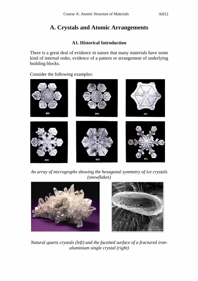

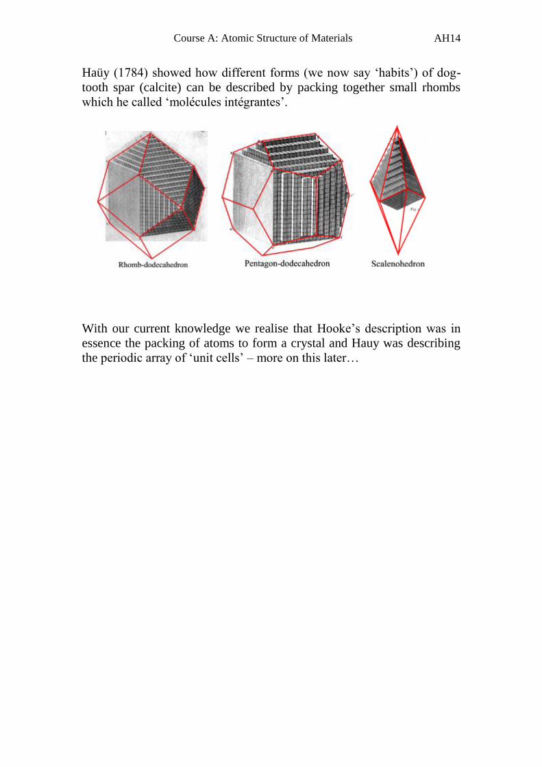

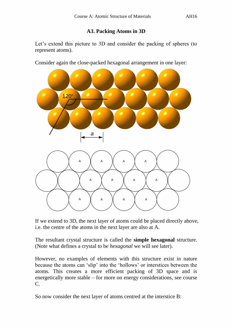
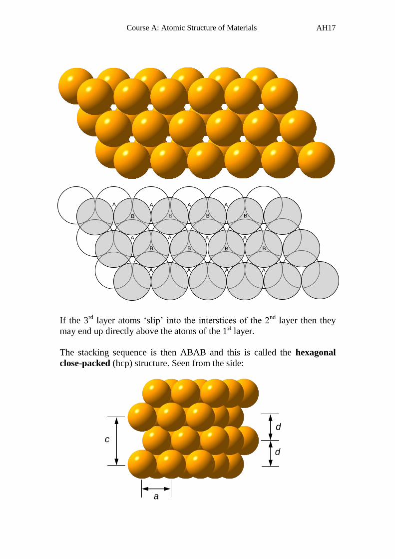
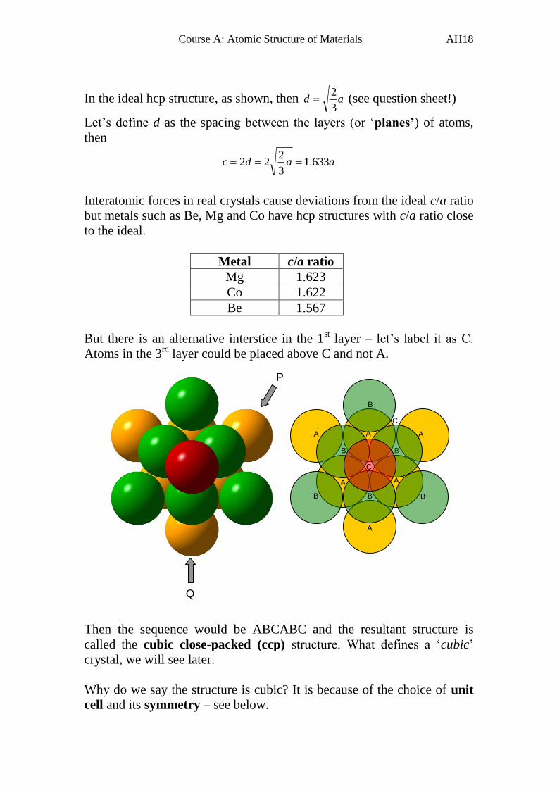


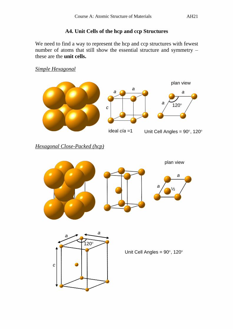


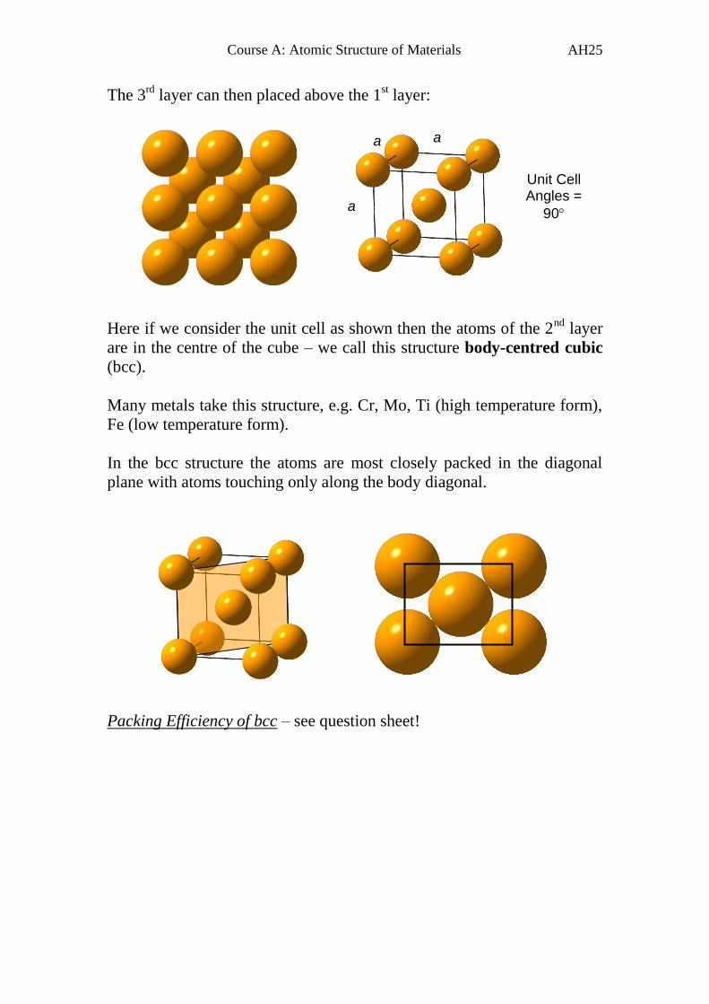
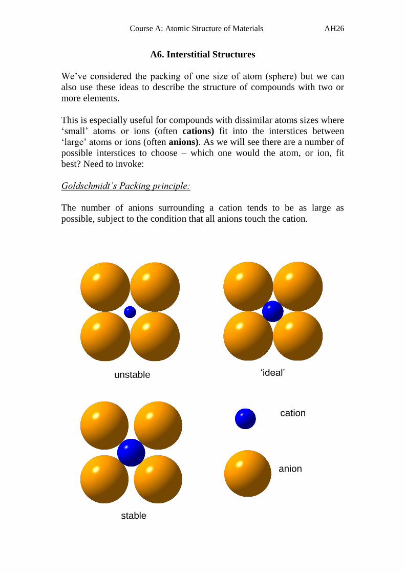
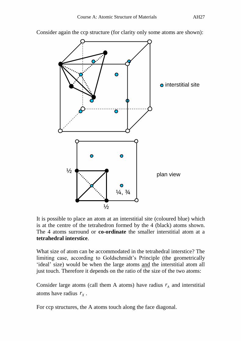
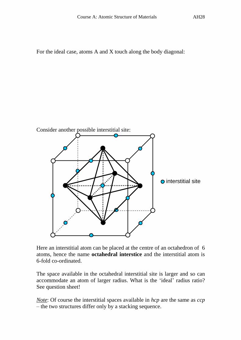

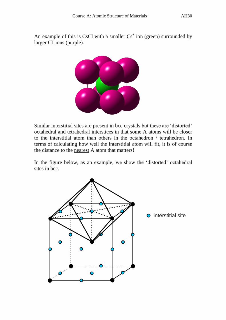
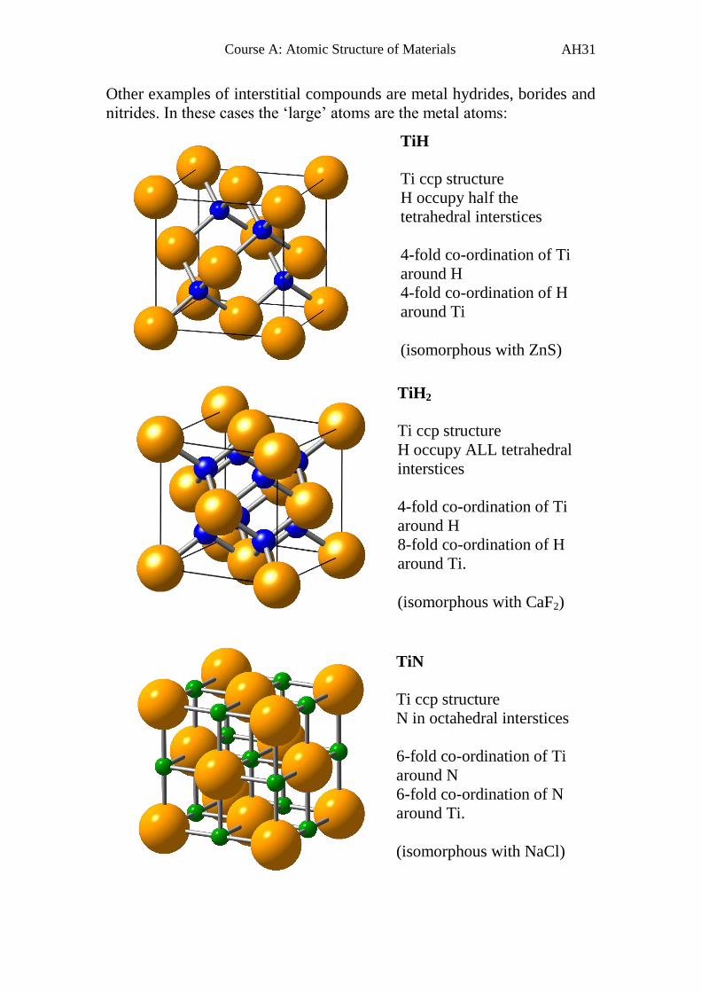
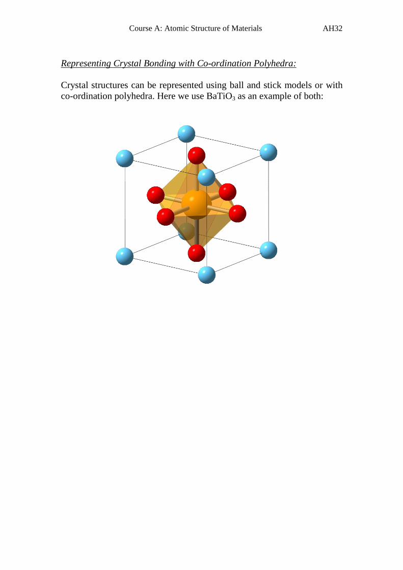


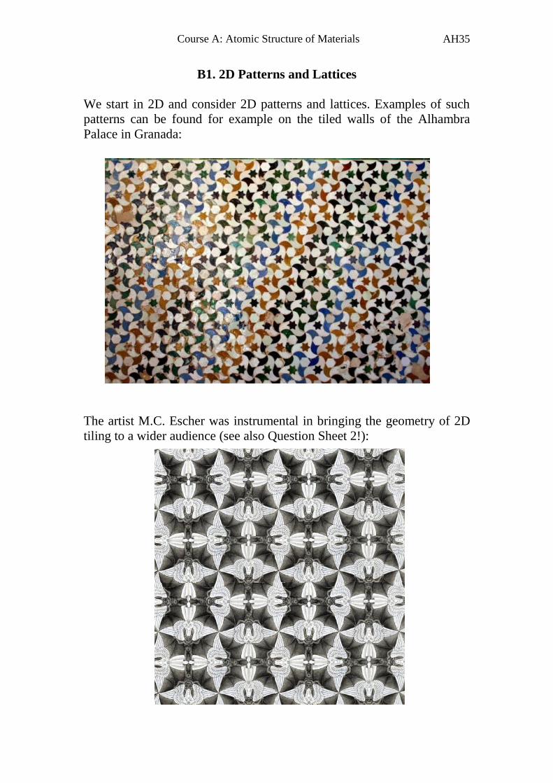


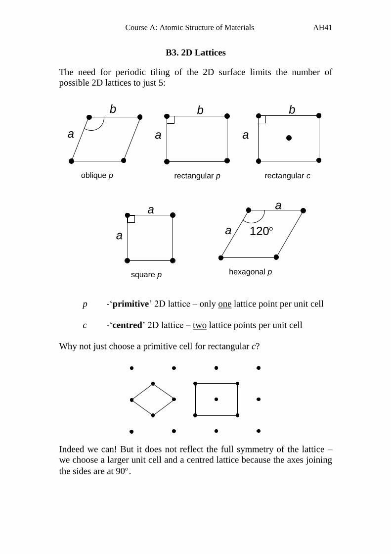
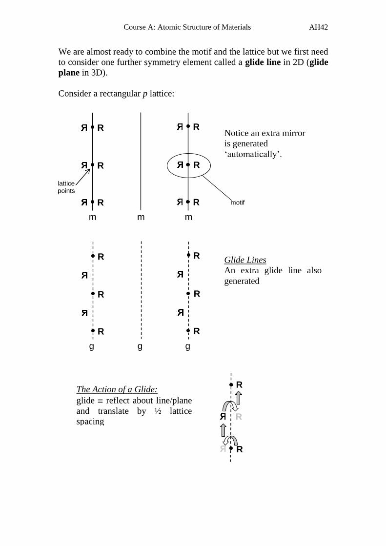
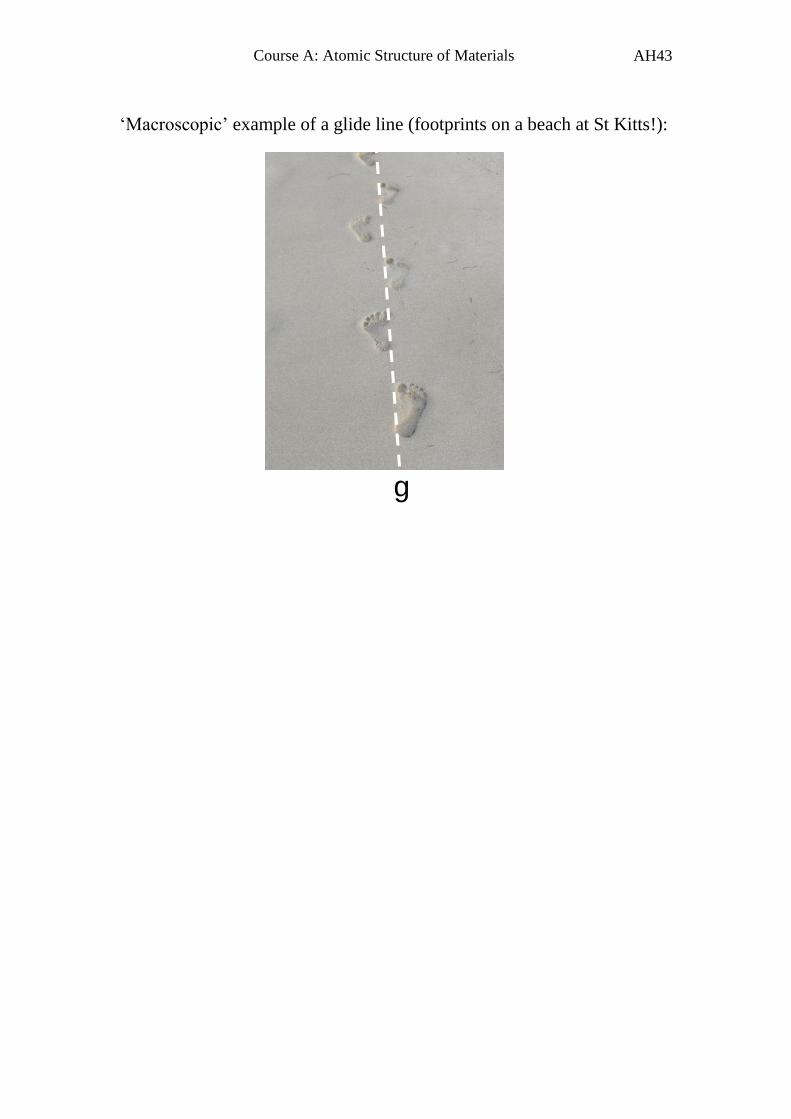

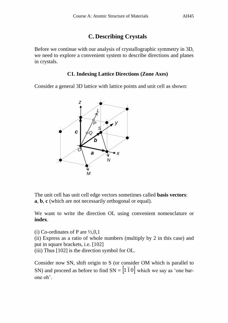
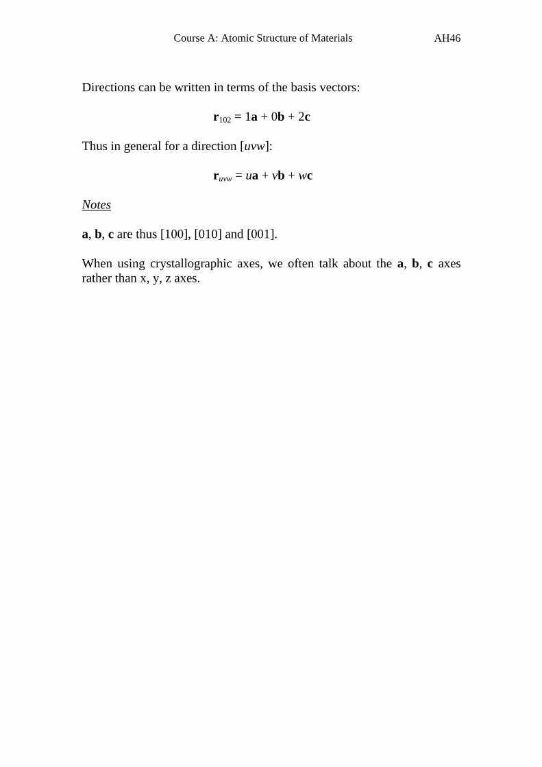
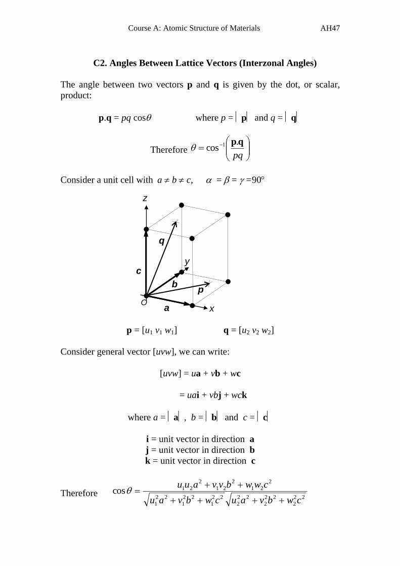

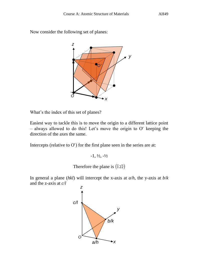


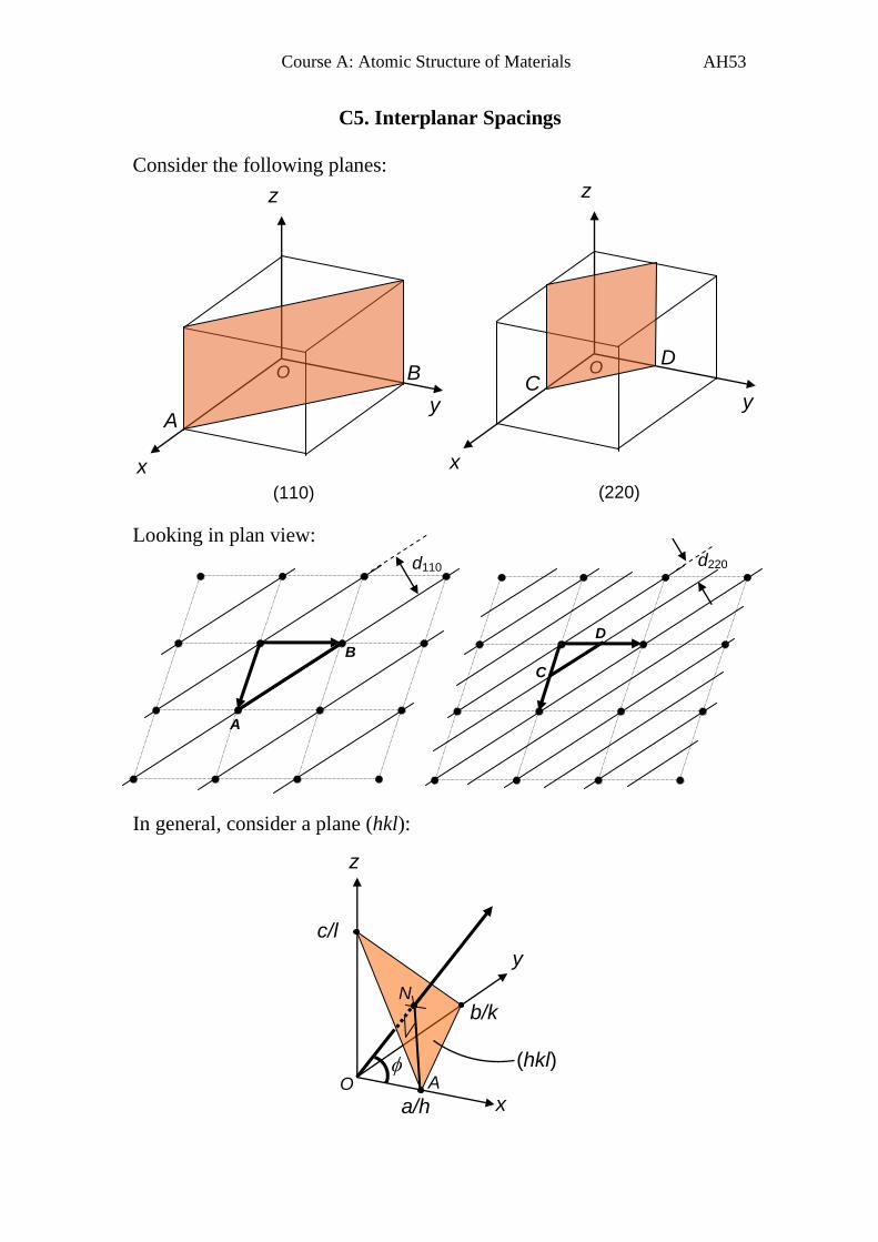
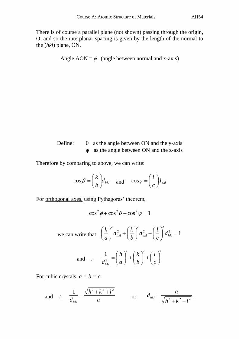
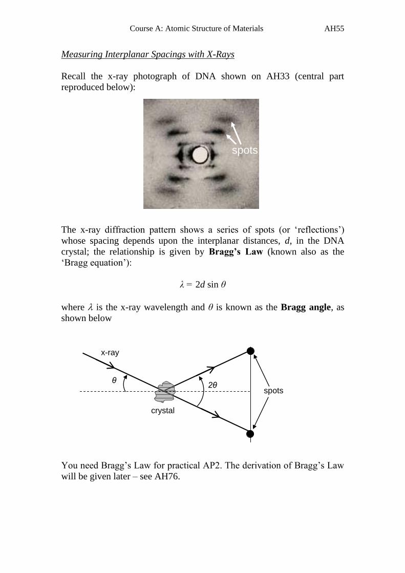


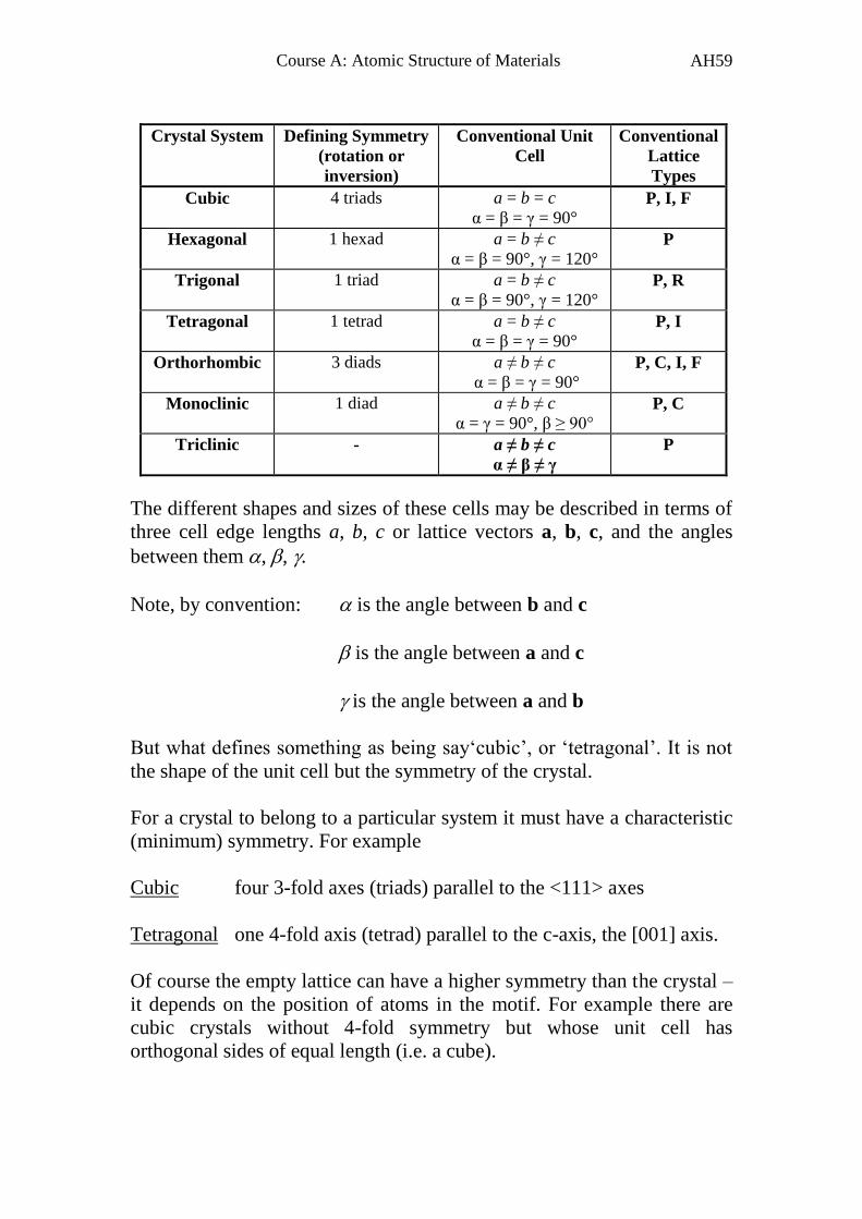
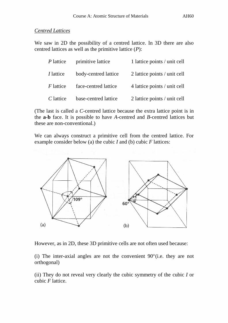
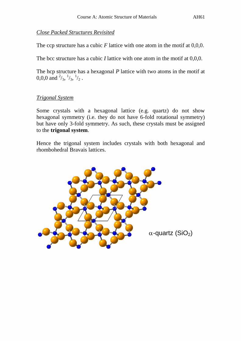

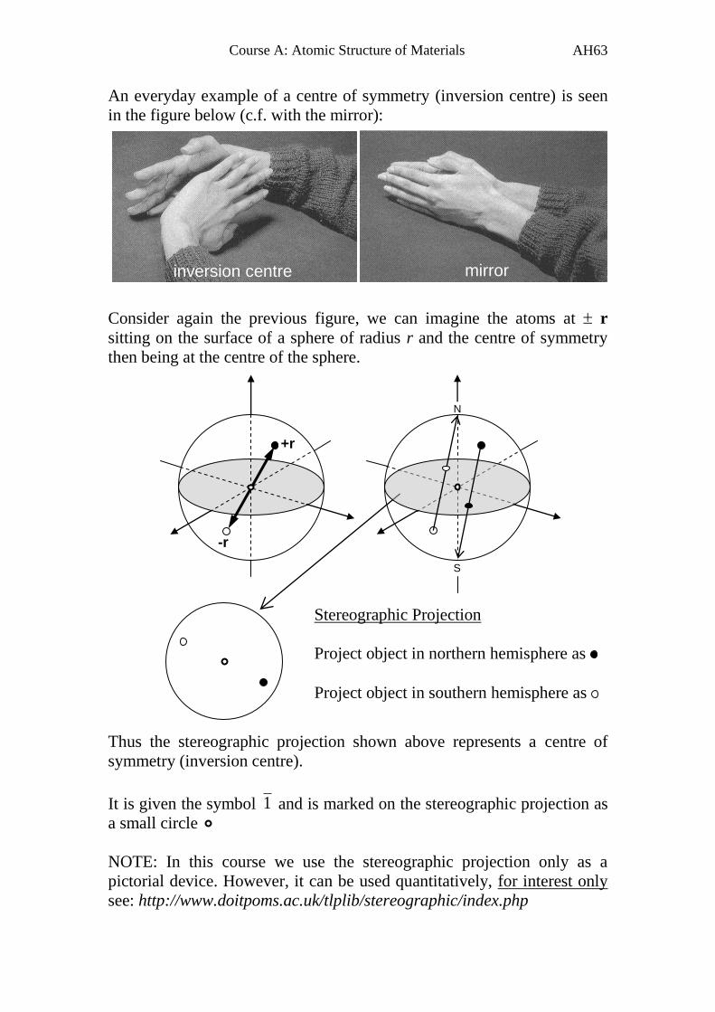


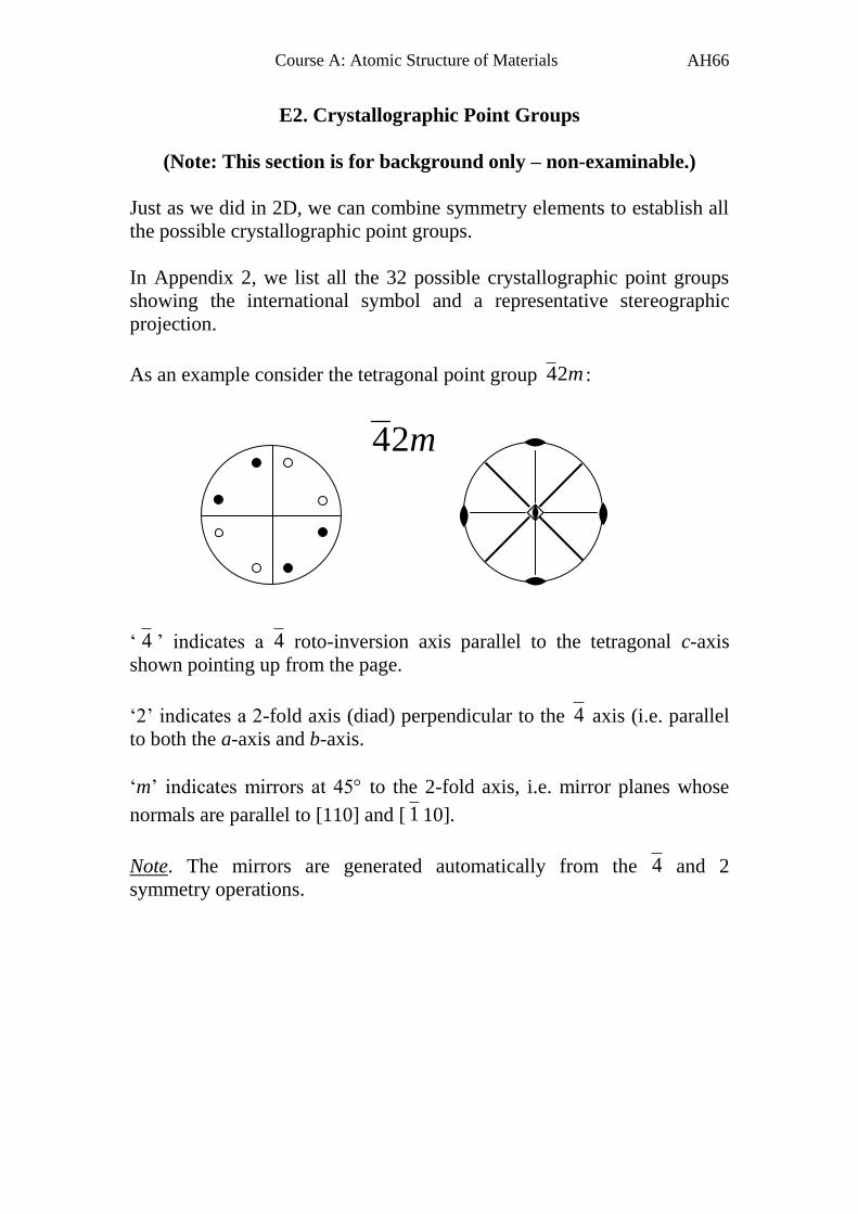


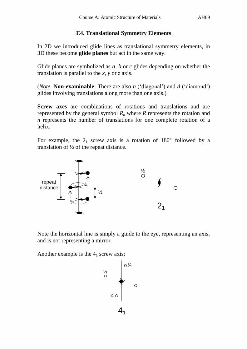
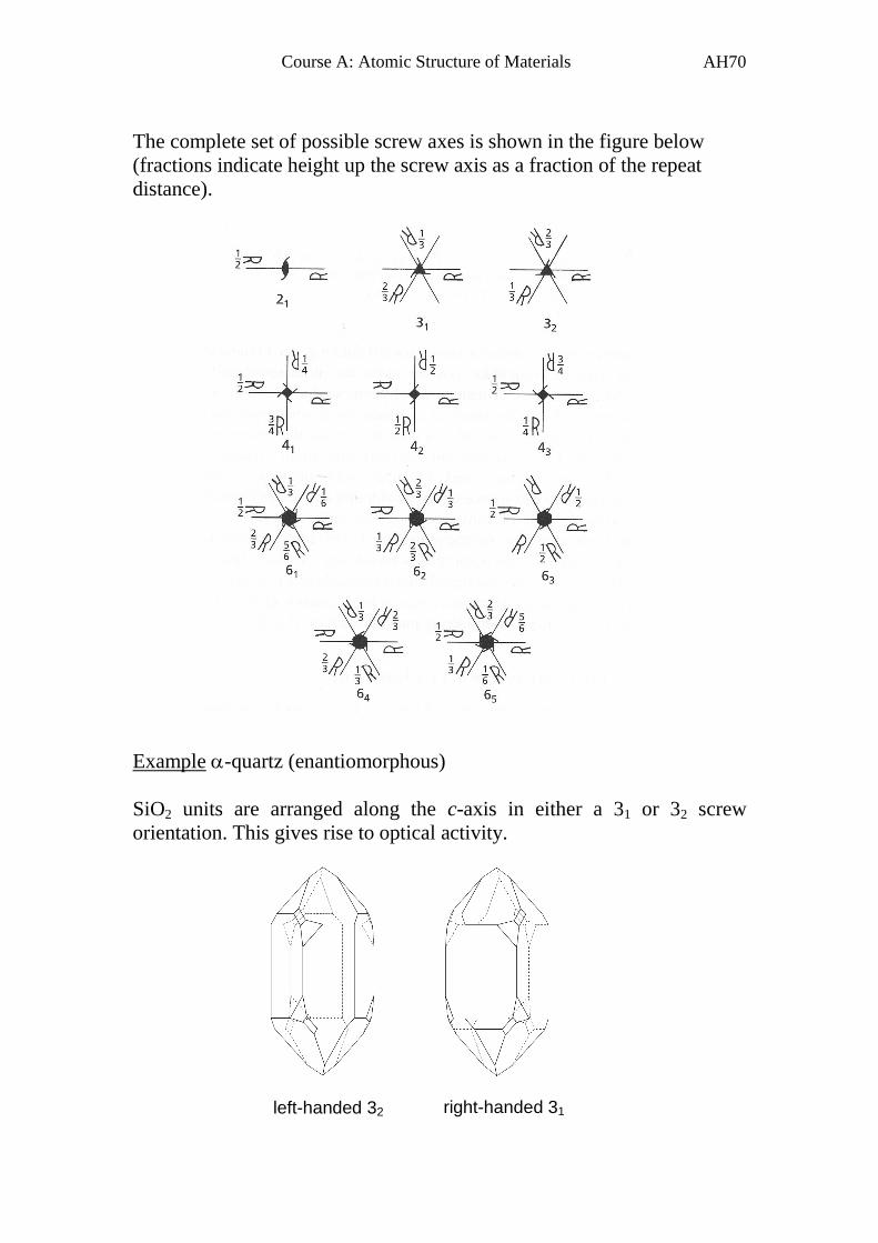

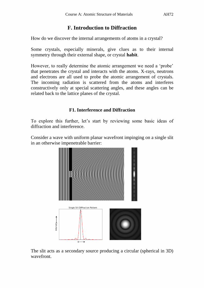


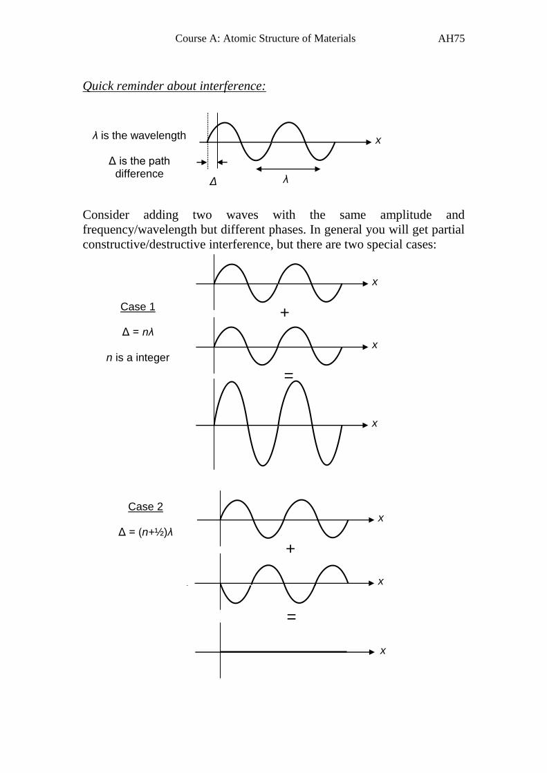


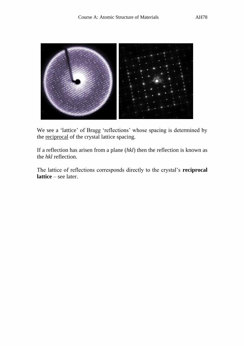
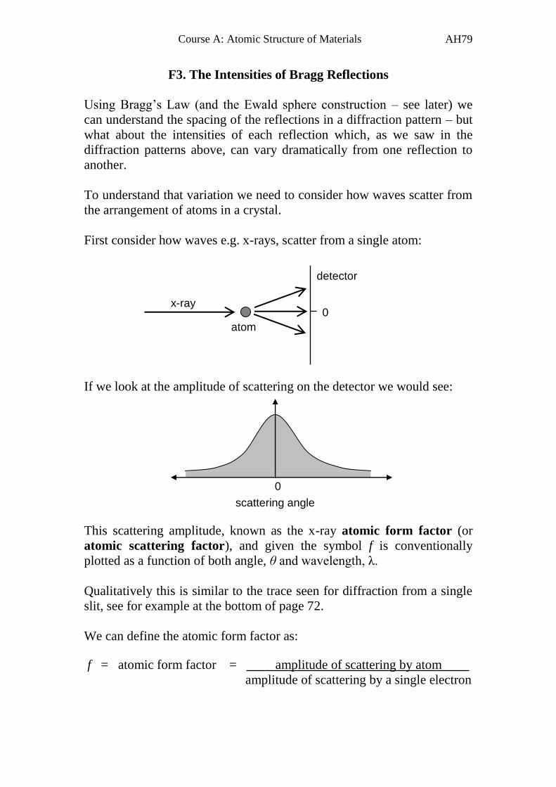
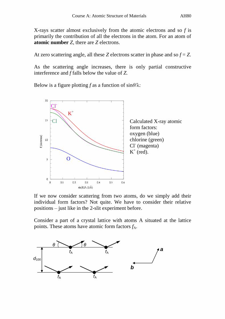

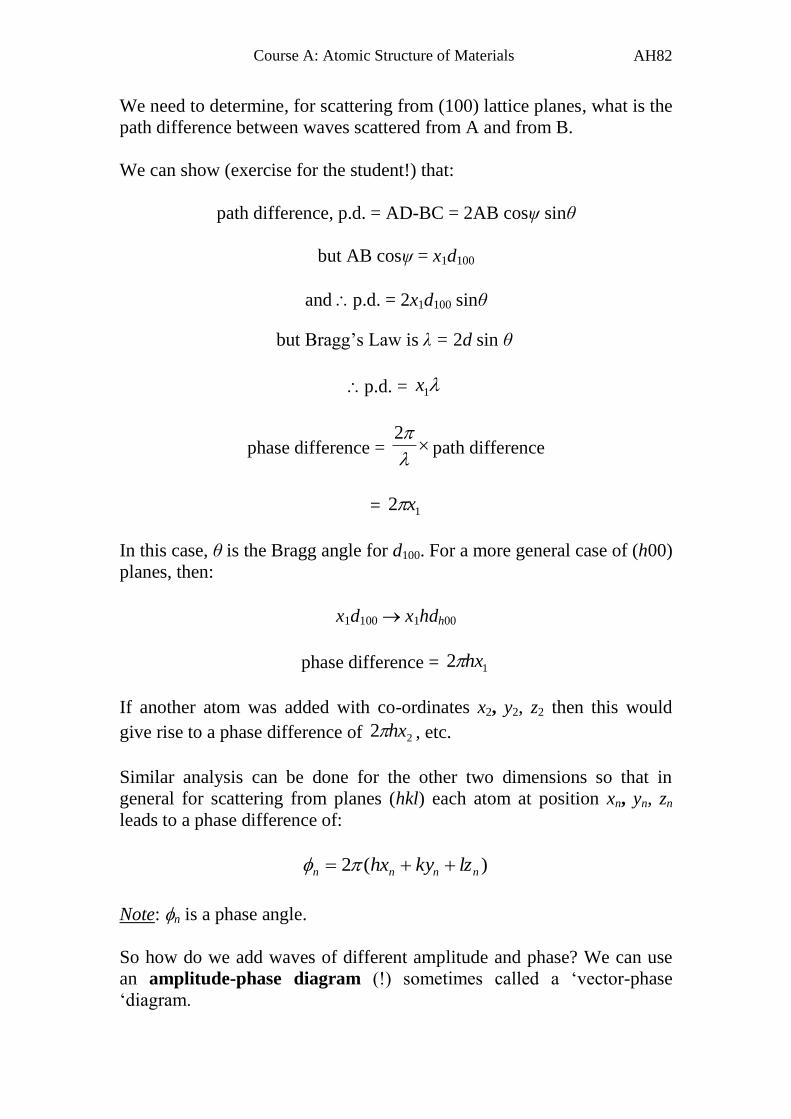


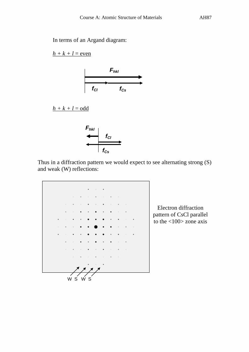
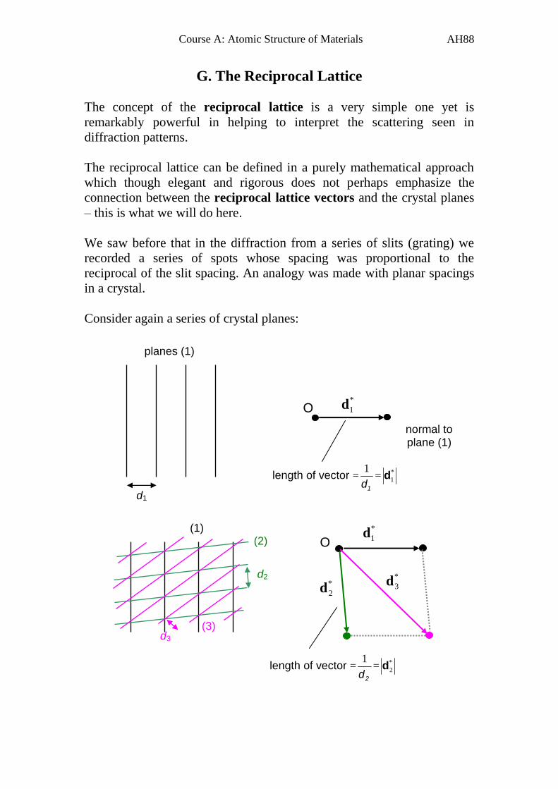


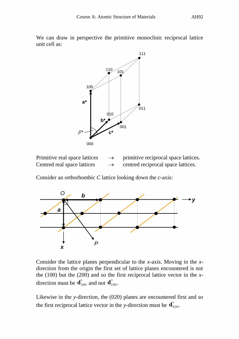
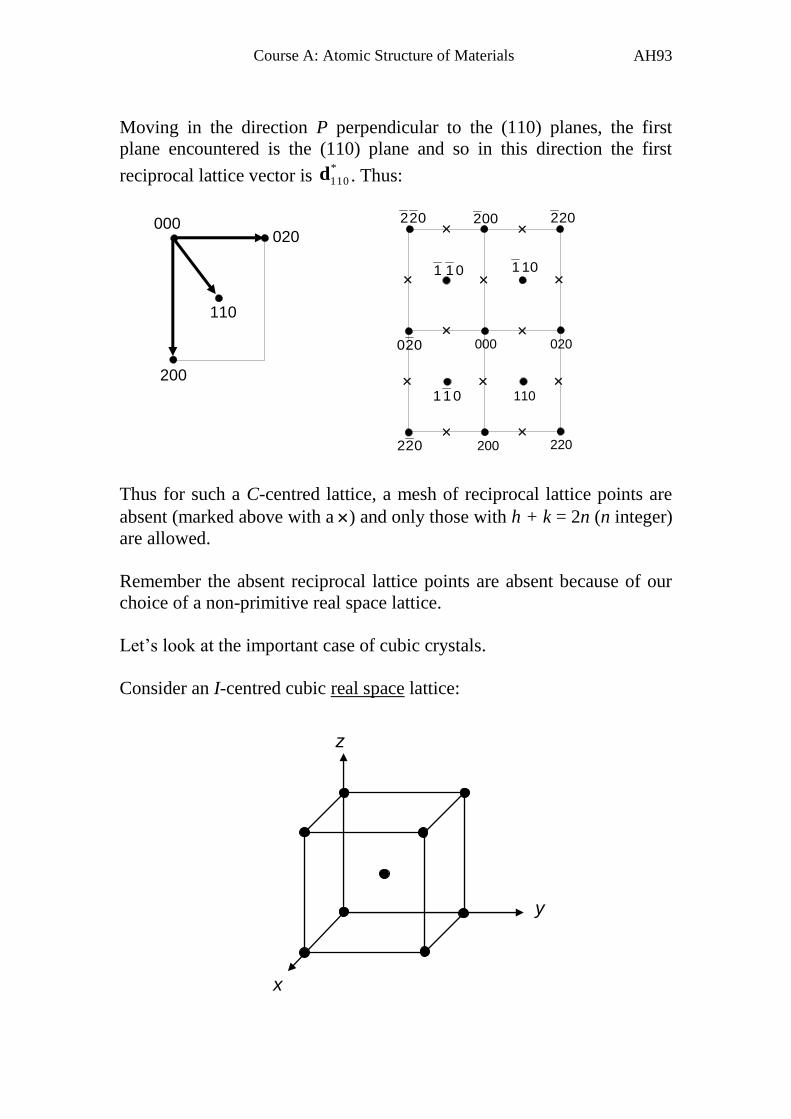

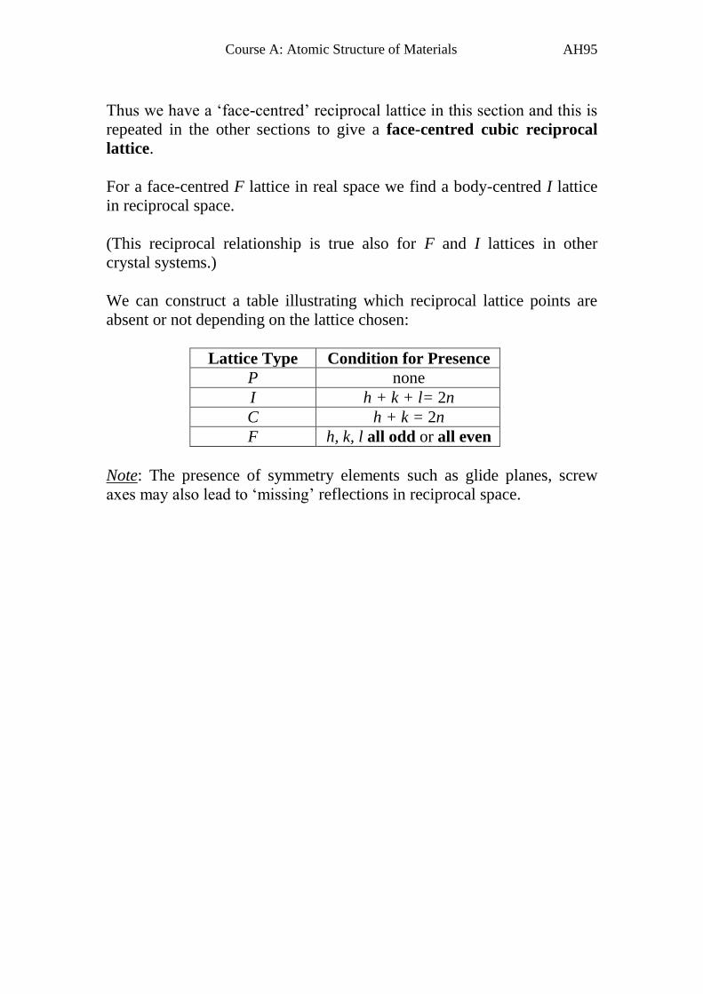

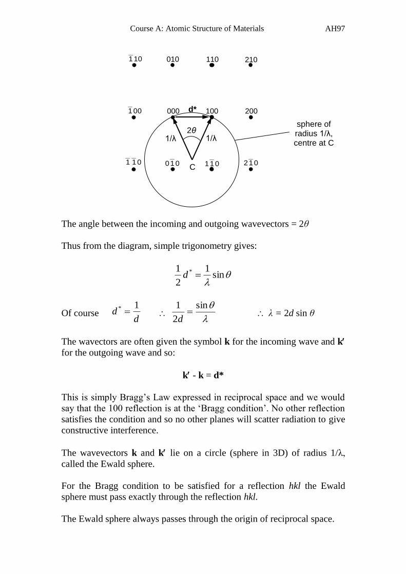


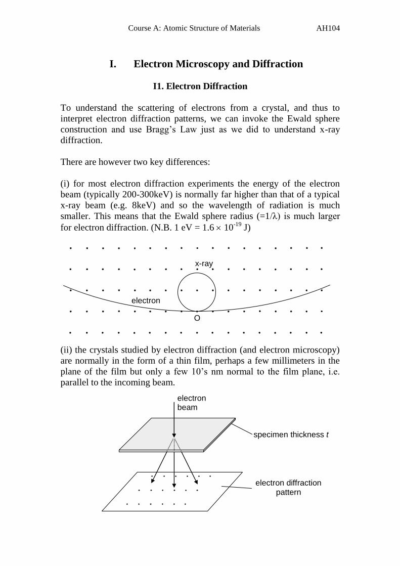

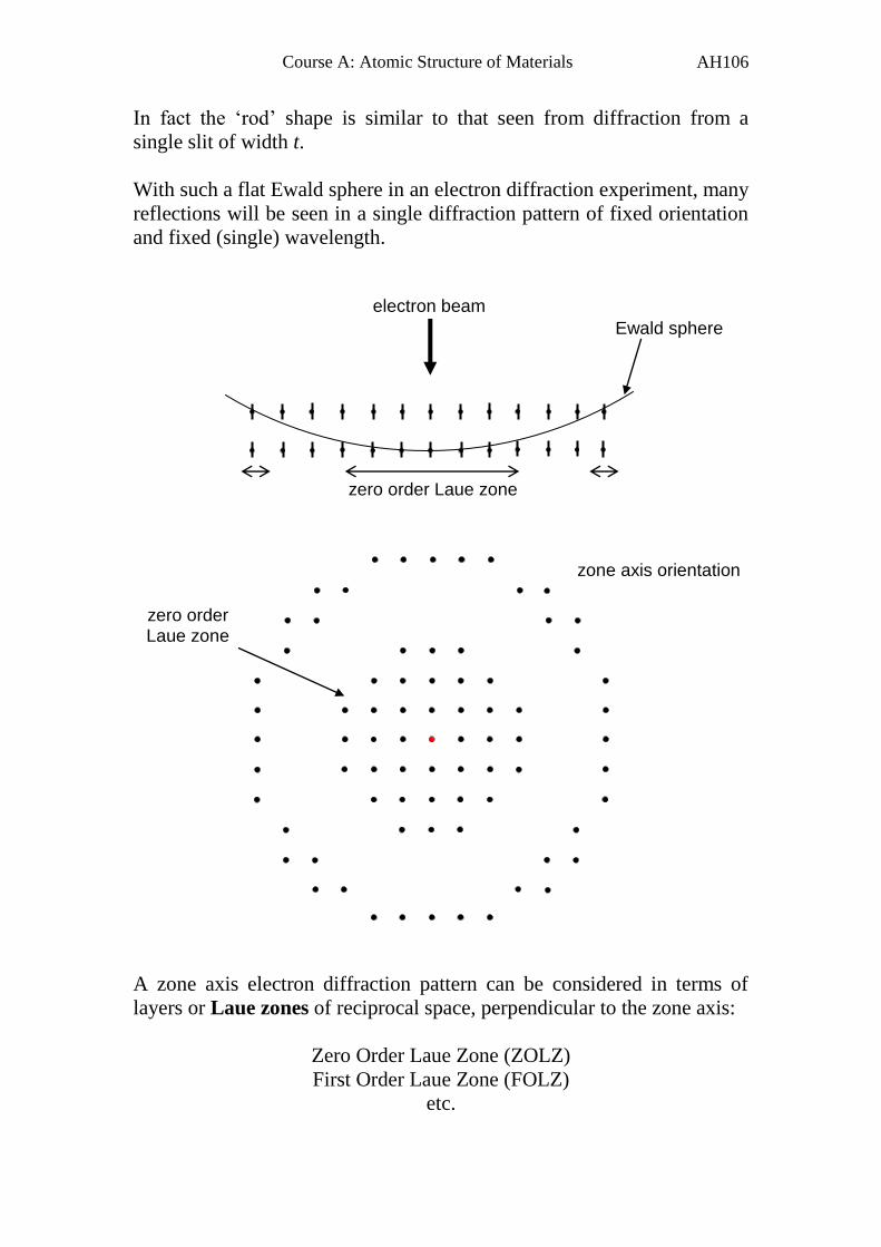
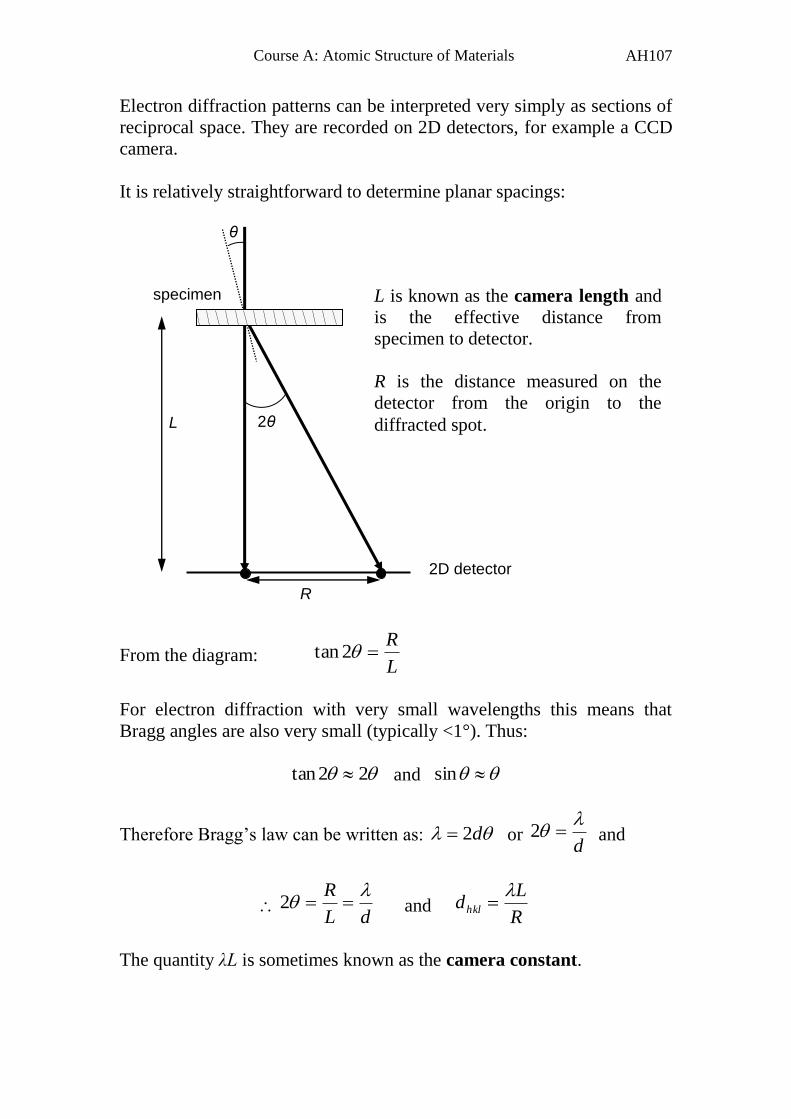
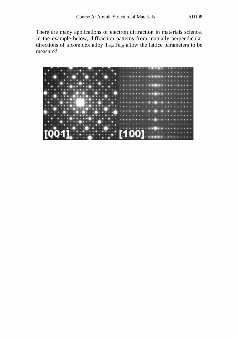


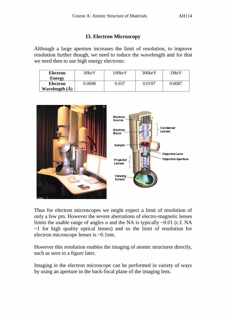
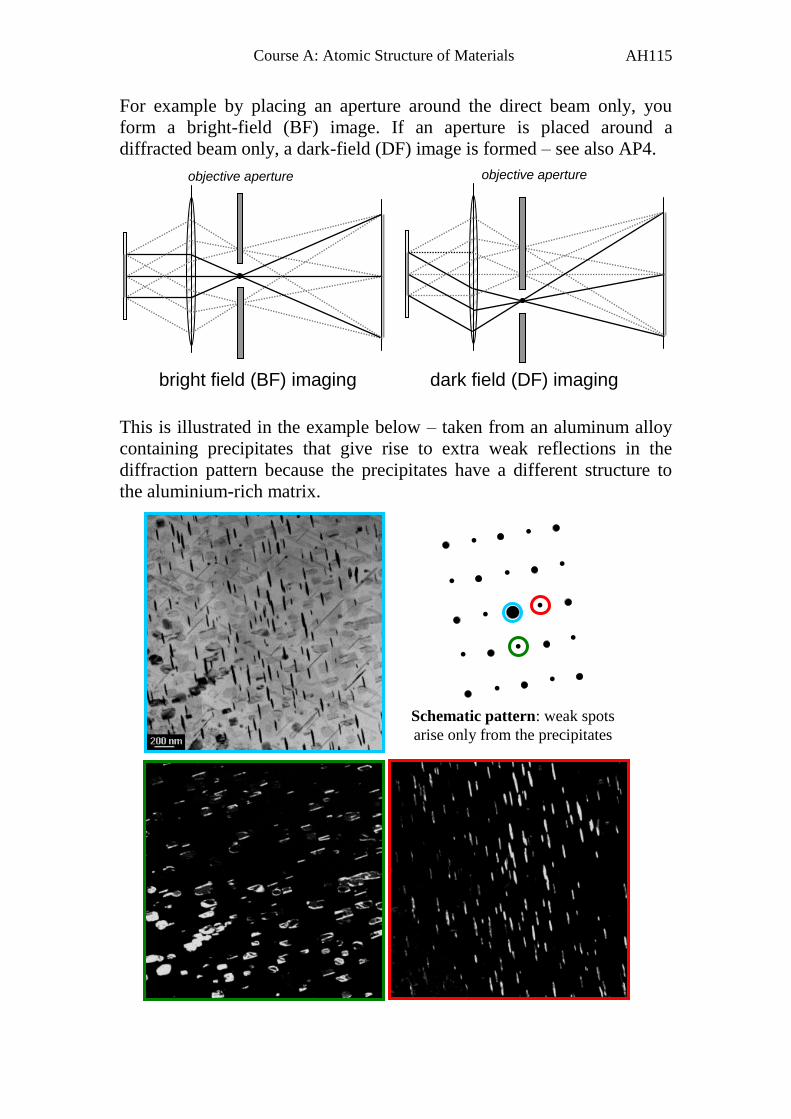


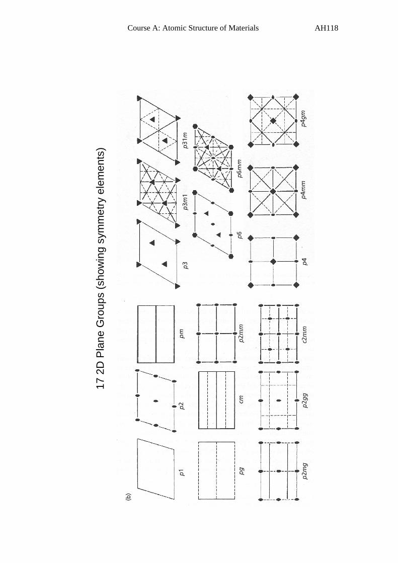

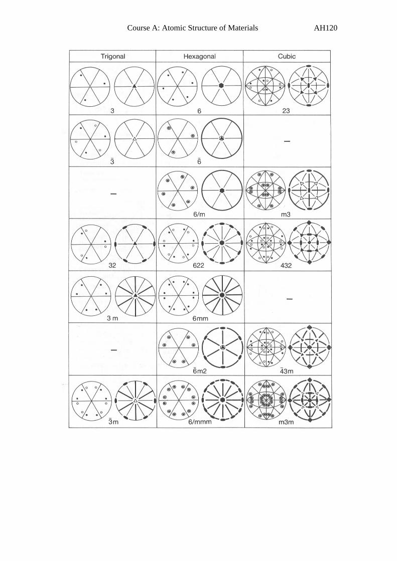

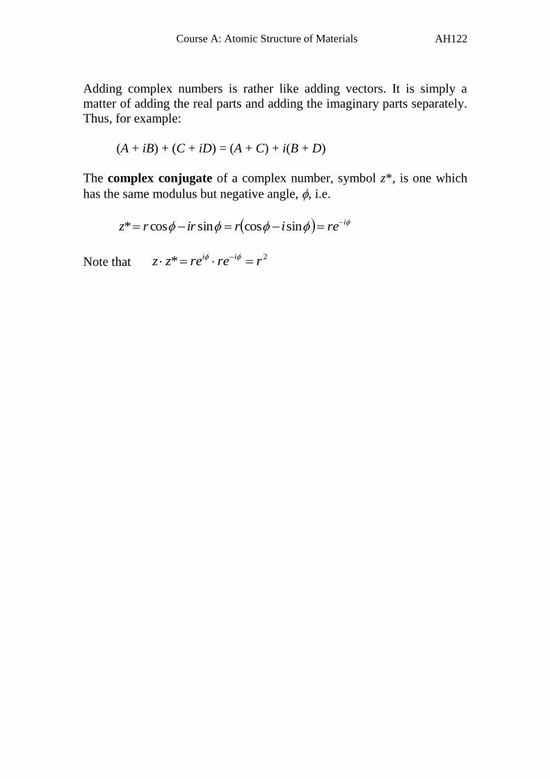


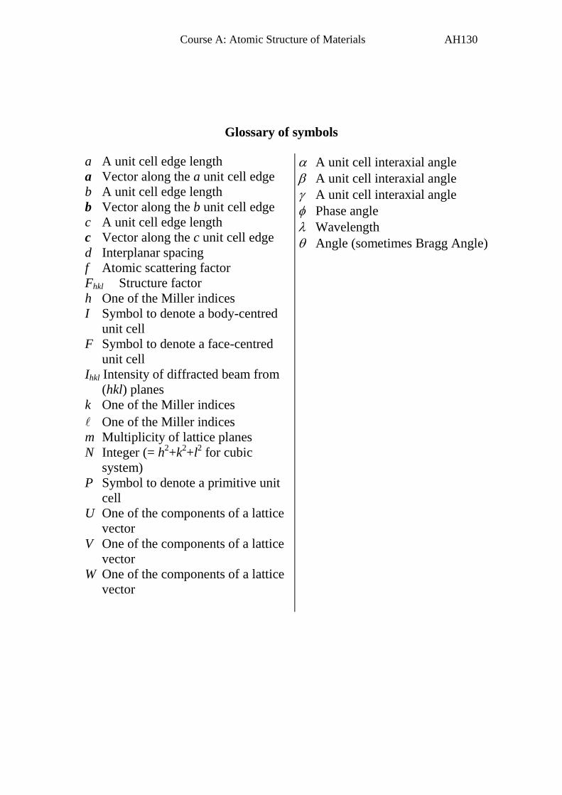

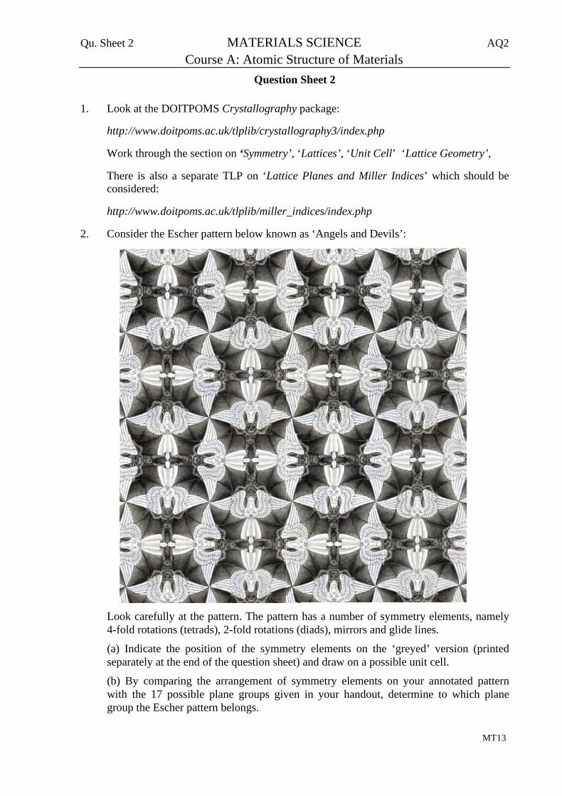
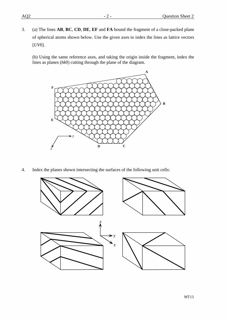
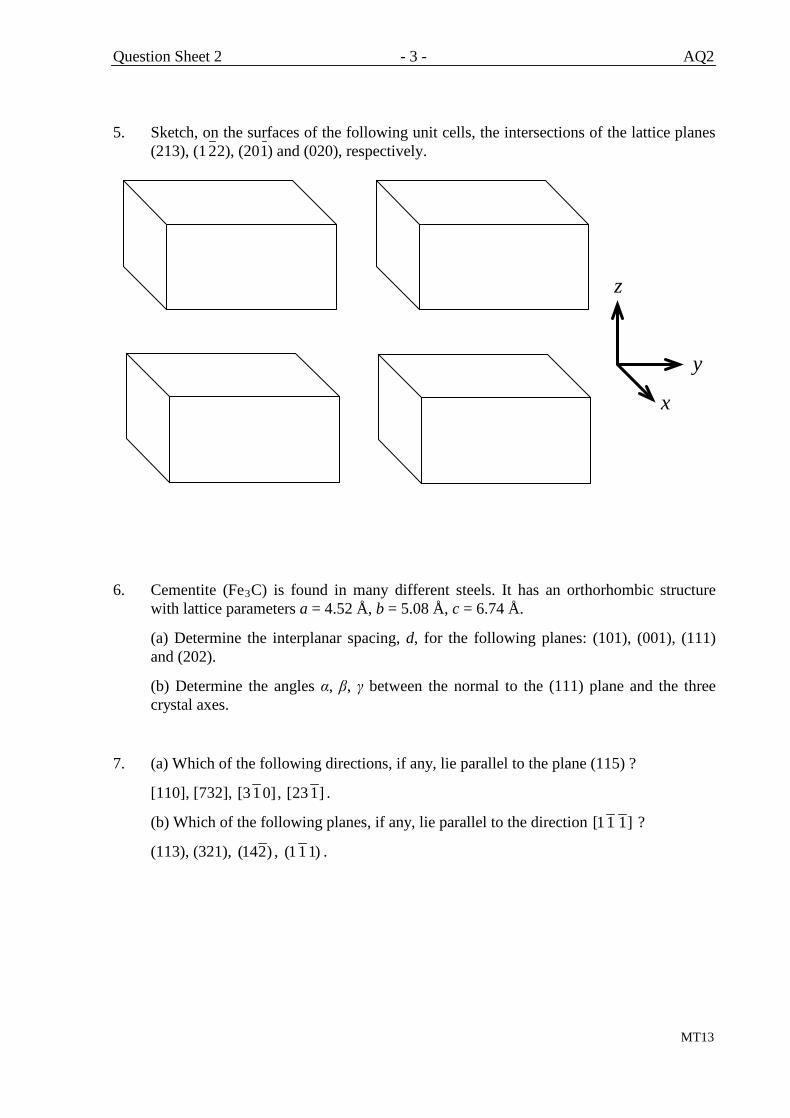


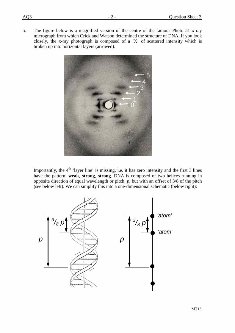


![[Disability] Justice Dictated by the Surfeit of Love ... · rights promote a kind of alienated and bourgeois ... [Disability] Justice Dictated by the Surfeit of ... to be directed](https://static.documents.pub/doc/80x56/5aefa1057f8b9abc788c3d9a/disability-justice-dictated-by-the-surfeit-of-love-promote-a-kind-of-alienated.jpg)


