Matlab/Simulink Generated FPGA Based Real-time HIL Simulator and DSP Controller: A Case Study Z. Süt ˝ o 1 , T. Debreceni 2 , T. Kökényesi 1 , A. Futó 1 and I. Varjasi 1 1 Department of Automation and Applied Informatics, Budapest University of Technology and Economics, Budapest, Hungary, E-mails: [email protected], [email protected], [email protected], [email protected]2 Siemens Hungary, E-mail: [email protected]Abstract. The paper reports the development of a case study for creating a unified development environment for the process of code generation from Matlab/Simulink into both HDL and C languages of FPGA and DSP targets. The FPGA is used for the Hardware-In-the-Loop (HIL) simulation of the high power, main circuit of a simple solar-based battery charger while the control functions belonging to this system are implemented in a DSP. The case study is planned to be a building block of the HIL simula- tion of either such a sophisticated, cyber-physical system like a microgrid which connects various forms of energy produced by renewable sources. Key words HIL Simulation, FPGA, Rapid Prototyping, Power Elec- tronics, Real-time Simulation 1. Introduction Nowadays as the technology is developing, the more com- plex the power electronics and its controls become, the more proper hardware tool is required for HIL simulation. The general aim of the presented work is developing a fast, reliable and scalable HIL simulation framework for the rapid prototyping of complex power electronic systems. There are at least three strong reasons for using HIL simu- lation during the development: i) reduction of development time, ii) safety and quality requirements, and iii) prevent costly and dangerous failures [1]. The main concept of using HIL simulation in power elec- tronic systems is that computational models replace the high-power parts of the system. The simulated parts are connected through real physical interfaces like analog and digital channels to the control boards under development, so the boards can be tested and validated in their seemingly real environment [2]. In HIL simulations the investigation of such practical issues like noise, sampling rate of the dig- ital controllers, delay in communication channels, nonzero bias of analog inputs and outputs and so on, can be readily Fig. 1. The main block diagram of the HIL simulator based test environment of the DSP controller. addressed. Since power electronic systems exhibit extremely fast, usu- ally quite complex and nonlinear dynamics due to the high- frequency switching action of the electronic switches, in this field nowadays the FPGA is becoming a possible can- didate for HIL simulations of the main circuits and com- ponents of the system (e.g. grid, battery, 3-phase IGBT Voltage Source Inverter, Motor Model etc.) [3], [4], [5]. 2. The Main Circuit Model The block diagram of the HIL simulator based test environ- ment of a DSP controller board can be seen in Fig. 1. Both DSP and FPGA boards are connected to a PC, and can be monitored and controlled by their HMIs. The whole case Fig. 2. Main circuit of the solar charger modeled in the HIL. https://doi.org/10.24084/repqj12.357 431 RE&PQJ, Vol.1, No.12, April 2014
Transcript
Matlab/Simulink Generated FPGA Based Real-time HIL Simulator and DSPController: A Case Study
Z. Süto1, T. Debreceni2, T. Kökényesi1, A. Futó1 and I. Varjasi1
Abstract. The paper reports the development of a case studyfor creating a unified development environment for the processof code generation from Matlab/Simulink into both HDL and Clanguages of FPGA and DSP targets. The FPGA is used for theHardware-In-the-Loop (HIL) simulation of the high power, maincircuit of a simple solar-based battery charger while the controlfunctions belonging to this system are implemented in a DSP. Thecase study is planned to be a building block of the HIL simula-tion of either such a sophisticated, cyber-physical system like amicrogrid which connects various forms of energy produced byrenewable sources.
Key words
HIL Simulation, FPGA, Rapid Prototyping, Power Elec-tronics, Real-time Simulation
1. Introduction
Nowadays as the technology is developing, the more com-plex the power electronics and its controls become, themore proper hardware tool is required for HIL simulation.The general aim of the presented work is developing afast, reliable and scalable HIL simulation framework forthe rapid prototyping of complex power electronic systems.There are at least three strong reasons for using HIL simu-lation during the development: i) reduction of developmenttime, ii) safety and quality requirements, and iii) preventcostly and dangerous failures [1].
The main concept of using HIL simulation in power elec-tronic systems is that computational models replace thehigh-power parts of the system. The simulated parts areconnected through real physical interfaces like analog anddigital channels to the control boards under development,so the boards can be tested and validated in their seeminglyreal environment [2]. In HIL simulations the investigationof such practical issues like noise, sampling rate of the dig-ital controllers, delay in communication channels, nonzerobias of analog inputs and outputs and so on, can be readily
Fig. 1. The main block diagram of the HIL simulator based testenvironment of the DSP controller.
addressed.
Since power electronic systems exhibit extremely fast, usu-ally quite complex and nonlinear dynamics due to the high-frequency switching action of the electronic switches, inthis field nowadays the FPGA is becoming a possible can-didate for HIL simulations of the main circuits and com-ponents of the system (e.g. grid, battery, 3-phase IGBTVoltage Source Inverter, Motor Model etc.) [3], [4], [5].
2. The Main Circuit Model
The block diagram of the HIL simulator based test environ-ment of a DSP controller board can be seen in Fig. 1. BothDSP and FPGA boards are connected to a PC, and can bemonitored and controlled by their HMIs. The whole case
Fig. 2. Main circuit of the solar charger modeled in the HIL.
https://doi.org/10.24084/repqj12.357 431 RE&PQJ, Vol.1, No.12, April 2014
Convert(SI)
Convert(SI)
value out
Sigma Delta
value out
Sigma Delta2
value out
Sigma Delta1
Convert(SI)
[currents]
[currents]
1
T
2
K
1
U_S_SD
2
I_L_SD
3
U_A_SD
voltages
currents
U_S0
R_S_1
U_A0
ChipScope
[voltages]
[voltages]U_S0
R_S^-1
U_A0
T
K
U_S
U_C2
I_L
I_A
U_D
U_A
SolarChargerHIL
Z-1Bitwise
ANDMasks
MSB
> 0
> 0
2^N
MSB1
1
value
1
out
(a)
(b)
Fig. 3. (a) Subsystem of the HIL simulator. (b) Sigma-delta D/A converter.
study was designed for learning the process of generatingcode for both FPGA and DSP.
The modeled system is a simple solar-based battery charger.The schematic diagram of the main circuit can be seen inFig. 2. The circuit is controlled by two logical input sig-nals, the PWM signal T controls the IGBT and the signal Kcontrols the DC contactor. The DSP controller measuresthree analog signals, the inductor current iL, the voltage ofthe solar panel uS and the battery voltage uA, and basedon these values and the charging current reference the con-troller fulfills the control actions. The solar panel is sub-stituted with a simple Thevenin model of a series voltagesource US0 and its inner resistance RS. UA0 is the no-loadbattery voltage which represents the actual state of chargeof the battery. US0, RS and UA0 are the main environmentalparameters used during our real-time testing.
To create the Simulink model of this dynamic system suit-able for generating the VHDL source files of the FPGA,firstly the functional description has to be done. The C1 ca-pacitor is charged up by the current from the Thevenin gen-erator, thus the voltage of the C1 will be the solar voltage uS.Essentially the next part — with the IGBT, diode D, induc-tance L and the capacitor C2 with the parallel dischargingresistor R — represents a step-down (buck) converter; thevoltage of the C2 capacitor has to be held by control of theiL current. By the control signal K of the DC contactorthe battery is connected and charged by current iA throughthe series inductor-resistor (LA-RA) of the inner impedancemodel of the accumulator.
The main circuit model was made by using state-spacemodeling [5, 6]. Let’s see the dynamic equations accordingto the dynamic components in form of integral equations:
uS =1
C1
∫ t
0
(US0 −uS
RS−TiL
)dt (1)
iL =1L
∫ t
0(uD −uC2)dt, where iL ≥ 0 (2)
uC2 =1
C2
∫ t
0
(iL − iA −
uC2
R2
)dt (3)
iA =1
LA
∫ t
0(uA −UA0 −RAiA)dt (4)
where the diode voltage uD can be expressed by the fol-
lowing piece-wise defined equation:
uD =
uS if T = 10 if T = 0 and iL > 0uC2 if T = 0 and iL = 0
(5)
Here ideal switching behaviors are assumed for both thediode and the IGBT. Due to the DC contactor model anadditional condition has to be fulfilled for the accumulatorvoltage uA:
uA =
uC2 if K = 1uC2 −Uarc if K = 0 and iA > 0UA0 if K = 0 and iA = 0
(6)
Uarc denotes the voltage of the electric arc developing if thecontactor is opened under non-zero current condition.
3. The HIL Simulator
The main block diagram of the HIL simulator can be seenin Fig. 3(a). It has logical input signals T and K comingfrom the DSP control board to the IGBT and the contac-tor. The DSP Control expects analog signals uS, uA and iLfrom the HIL. However analog signals directly cannot beoutputted by the FPGA, sigma-delta D/A converters wereused [see Fig. 3(b)]. This D/A converter type is very sim-ilar to a PWM generator: the generated duty cycle at theoutput will be proportional to the input value. In order toreach the proportional analog value, analog filters (RC cir-cuits) are required to connect the corresponding FPGA legsto the A/D channels of the DSP controller (Fig. 1). Notethat, filters with higher cut-off frequency can be applied forsigma-delta signals than for PWM signals, so sigma-deltaD/A converters are able to generate faster analog signals.
The Xilinx’s ChipScope Pro is a utility tool for viewingand/or modifying inner signals in the FPGA at runningtime. By means of this utility HMI can be created to adesign, for example to set parameters such as the actualinsolation level of the solar panel by the US0 voltage orthe state of charge of the accumulator by its UA0 no-loadvoltage. The ChipScope subsystem placed in the model inFig. 3(a) is an empty subsystem block, only its interfaceis defined by the input and output signals. The HDL ar-chitecture property of this subsystem block is defined as
https://doi.org/10.24084/repqj12.357 432 RE&PQJ, Vol.1, No.12, April 2014
== 0
> 0
dt/C1 Z-1
dt/C2 Z-1
1024/R2
dt/L Z-1
dt/L_A
Z-1
R_A
1
U_S0
2
R_S^-1
4
T
5
K
3
U_A0
1
U_S
2
U_C2
3
I_L
4
I_A
U_arc> 0
ANDNOT
OR
> 0
> 05
U_D
> 0
> 0
6
U_A
> 0
> 0> 0
Convert
Convert
Convert
Convert
Z-1
Z-1
Z-1 Z-1
Z-1 [R_S1]
[R_S1]
[U_S0]
[U_S0]
[T]
[T]
[T]
[U_S]
[U_S]
[U_D]
[U_S]
[i_L]
[I_L]
[U_C2]
[U_C2]
[I_L]
[I_L]
[U_C2]
[U_C2]
[K]
[K]
[I_A]
[I_A]
[I_A]
[I_A]
[K2]
[K2]
[U_A0]
[U_A0]
[U_A]
[U_A]
[U_A0]
[U_C2]
[U_D]
(a)
(b)
(c)
(d)
(e)
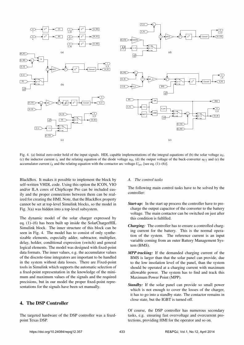
Fig. 4. (a) Initial zero-order hold of the input signals. HDL capable implementations of the integral equations of (b) the solar voltage uS,(c) the inductor current iL and the relating equation of the diode voltage uD, (d) the output voltage of the buck-converter uC2 and (e) theaccumulator current iA and the relating equation with the contactor arc voltage Uarc [see eq. (1)–(6)].
BlackBox. It makes it possible to implement the block byself-written VHDL code. Using this option the ICON, VIOand/or ILA cores of ChipScope Pro can be included eas-ily and the proper connections between them can be real-ized for creating the HMI. Note, that the BlackBox propertycannot be set at top-level Simulink blocks, so the model inFig. 3(a) was hidden into a top-level subsystem.
The dynamic model of the solar charger expressed byeq. (1)–(6) has been built up inside the SolarChargerHILSimulink block. The inner structure of this block can beseen in Fig. 4. The model has to consist of only synthe-sizable elements, especially adder, subtractor, multiplier,delay, holder, conditional expression (switch) and generallogical elements. The model was designed with fixed-pointdata formats. The inner values, e.g. the accumulator valuesof the discrete-time integrators are important to be handledin the system without data losses. There are Fixed-pointtools in Simulink which supports the automatic selection ofa fixed-point representation in the knowledge of the mini-mum and maximum values of the signals and the requiredprecisions, but in our model the proper fixed-point repre-sentations for the signals have been set manually.
4. The DSP Controller
The targeted hardware of the DSP controller was a fixed-point Texas DSP.
A. The control tasks
The following main control tasks have to be solved by thecontroller:
Start-up: In the start up process the controller have to pre-charge the output capacitor of the converter to the batteryvoltage. The main contactor can be switched on just afterthis condition is fulfilled.
Charging: The controller has to ensure a controlled charg-ing current for the battery. This is the normal opera-tion of the system. The reference current is an inputvariable coming from an outer Battery Management Sys-tem (BMS).
MPP tracking: If the demanded charging current of theBMS is larger than that the solar panel can provide, dueto the low insolation level of the panel, than the systemshould be operated at a charging current with maximumallowable power. The system has to find and track thisMaximum Power Point (MPP).
Standby: If the solar panel can provide so small powerwhich is not enough to cover the losses of the charger,it has to go into a standby state. The contactor remains inclose state, but the IGBT is turned off.
Of course, the DSP controller has numerous secondarytasks, e.g. ensuring fast overvoltage and overcurrent pro-tections, providing HMI for the operator and so on.
https://doi.org/10.24084/repqj12.357 433 RE&PQJ, Vol.1, No.12, April 2014
ADC_int()
sensors
SM_controls
controls
duty_cycle
FastTask
C28x
Interrupt
IRQ11
C28x Hardware Interrupt
SCIComm
Db_buf
Rate Transition
Db_buf
Rate Transition1
ADC_int()
sensors
reset
ReadInputs
f
ADC_int()
controls
SetOutputs
f
sensors
reset
duty_cycle
SM_controls
StateMachine
Db_buf
Rate Transition2
Target Preferences
Copy
Rate Transition3
[duty_cycle]
Goto
[duty_cycle]
From
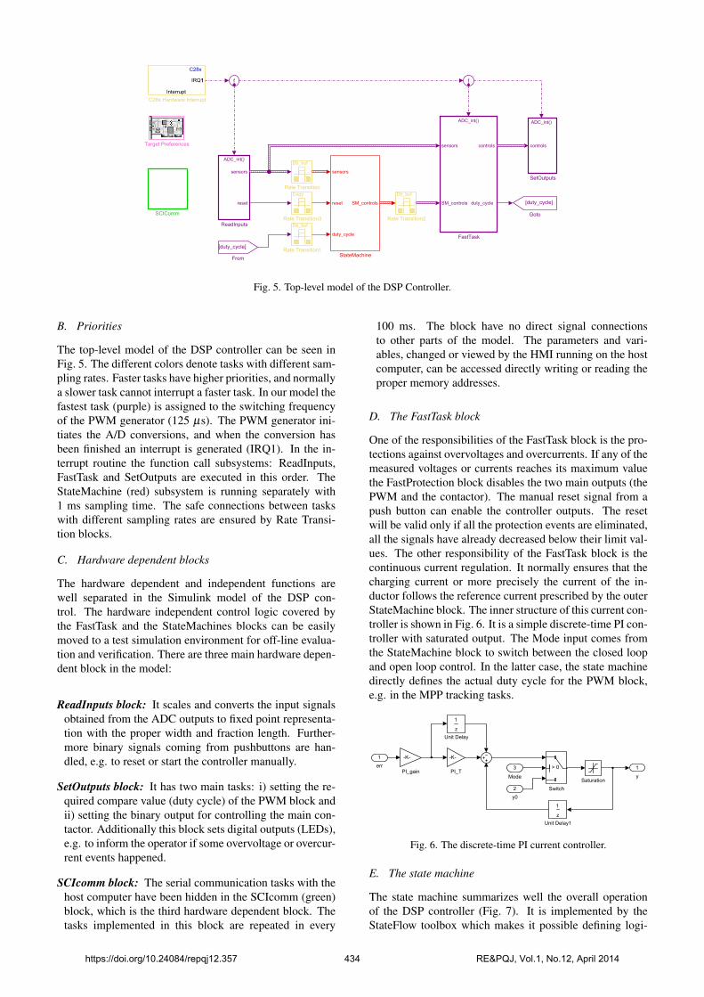
Fig. 5. Top-level model of the DSP Controller.
B. Priorities
The top-level model of the DSP controller can be seen inFig. 5. The different colors denote tasks with different sam-pling rates. Faster tasks have higher priorities, and normallya slower task cannot interrupt a faster task. In our model thefastest task (purple) is assigned to the switching frequencyof the PWM generator (125 µs). The PWM generator ini-tiates the A/D conversions, and when the conversion hasbeen finished an interrupt is generated (IRQ1). In the in-terrupt routine the function call subsystems: ReadInputs,FastTask and SetOutputs are executed in this order. TheStateMachine (red) subsystem is running separately with1 ms sampling time. The safe connections between taskswith different sampling rates are ensured by Rate Transi-tion blocks.
C. Hardware dependent blocks
The hardware dependent and independent functions arewell separated in the Simulink model of the DSP con-trol. The hardware independent control logic covered bythe FastTask and the StateMachines blocks can be easilymoved to a test simulation environment for off-line evalua-tion and verification. There are three main hardware depen-dent block in the model:
ReadInputs block: It scales and converts the input signalsobtained from the ADC outputs to fixed point representa-tion with the proper width and fraction length. Further-more binary signals coming from pushbuttons are han-dled, e.g. to reset or start the controller manually.
SetOutputs block: It has two main tasks: i) setting the re-quired compare value (duty cycle) of the PWM block andii) setting the binary output for controlling the main con-tactor. Additionally this block sets digital outputs (LEDs),e.g. to inform the operator if some overvoltage or overcur-rent events happened.
SCIcomm block: The serial communication tasks with thehost computer have been hidden in the SCIcomm (green)block, which is the third hardware dependent block. Thetasks implemented in this block are repeated in every
100 ms. The block have no direct signal connectionsto other parts of the model. The parameters and vari-ables, changed or viewed by the HMI running on the hostcomputer, can be accessed directly writing or reading theproper memory addresses.
D. The FastTask block
One of the responsibilities of the FastTask block is the pro-tections against overvoltages and overcurrents. If any of themeasured voltages or currents reaches its maximum valuethe FastProtection block disables the two main outputs (thePWM and the contactor). The manual reset signal from apush button can enable the controller outputs. The resetwill be valid only if all the protection events are eliminated,all the signals have already decreased below their limit val-ues. The other responsibility of the FastTask block is thecontinuous current regulation. It normally ensures that thecharging current or more precisely the current of the in-ductor follows the reference current prescribed by the outerStateMachine block. The inner structure of this current con-troller is shown in Fig. 6. It is a simple discrete-time PI con-troller with saturated output. The Mode input comes fromthe StateMachine block to switch between the closed loopand open loop control. In the latter case, the state machinedirectly defines the actual duty cycle for the PWM block,e.g. in the MPP tracking tasks.
Saturation
1
err 1
y
z
1
Unit Delay
z
1
Unit Delay1
-K-
PI_gain
-K-
PI_T > 0
Switch2
y0
3
Mode
Fig. 6. The discrete-time PI current controller.
E. The state machine
The state machine summarizes well the overall operationof the DSP controller (Fig. 7). It is implemented by theStateFlow toolbox which makes it possible defining logi-
https://doi.org/10.24084/repqj12.357 434 RE&PQJ, Vol.1, No.12, April 2014
cal type control in a more powerful way comparing to theother parts of Simulink. At power on the system enters intothe Start state. When the outer BMS requests a chargingcurrent and the environment is good, that is, the insolationlevel of the solar panel is enough for charging, the controllerpre-charges first the output capacitor of the buck converterwith a small current. The output capacitor voltage is notmeasured, only estimated. The pre-charging current used issmall, but large enough to operate the converter in contin-uous current conduction mode. Keeping this condition, thebuck converter output voltage can be calculated as the mul-tiplication of the duty cycle and the measured input solarvoltage. When the pre-charging condition is fulfilled, thecurrent controller is stopped, and the contactor is switchedon. After a safety delay time, the state machine enters intothe contactor closed state and start to manage the charging,maximum power point tracking and the standby states.
5. Real-time HIL tests of the DSP Controller
The overall case study with the FPGA and the DSP boardsand with the interconnections between them is built up onan intelligent breadboard equipped with some instrumentsfor measuring and generating signals (Fig. 8).
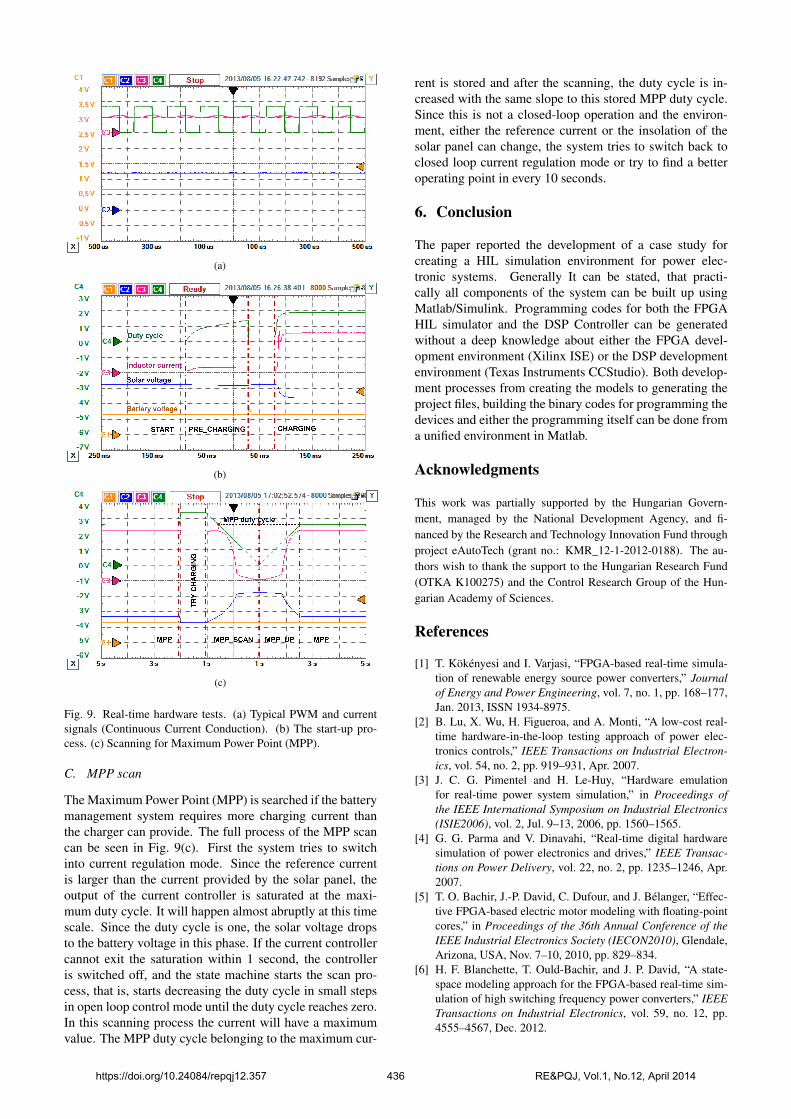
A. Closed-loop current regulation
The oscilloscope diagram in Fig. 9(a) shows the normal op-erating mode of the system, which is the closed loop currentregulation. Typical signals measured between the HIL andthe DSP are shown on the display in steady-state of the con-troller. The green curve is the PWM signal, the dark pink isthe inductor current. The current ripple caused by the PWMcan be observed well. The other two signals, the solar volt-age (blue) and the battery voltage (orange) are practicallyconstant at this time scale.
B. The start-up process
The pre-charging state and than the start of the current reg-ulation is shown in Fig. 9(b). Since the time scale is largethe oscilloscope averages out the PWM signal, so the greencurve represents the duty cycle. The pre-charging currentis just about 10 percent of the maximum current which wasapplied in the charging phase at the right hand side of the di-agram. As the current reaches its steady-state and becomesalmost constant, the duty cycle is increasing near linearlyto the end of the pre-charging phase. It means that the ef-fect of the load resistance at the output of the converter isnegligible, the output capacitor of the converter is chargedpractically by a current source. A transient peak can beseen on the battery voltage when the contactor is closed. Ithappens just after the pre-charging state was finished, sincethe mechanical delay of the contactor is not modeled in theHIL. However the controller waits 50 ms for the contactorclosing before it starts the battery charging. Entering intothe charging state, the reference current jumps to a highervalue and the solar voltage drops to a smaller value at thesame time since the solar panel is loaded more heavily.
Fig. 8. Built-up on intelligent breadboard.
https://doi.org/10.24084/repqj12.357 435 RE&PQJ, Vol.1, No.12, April 2014
(a)
(b)
(c)
Fig. 9. Real-time hardware tests. (a) Typical PWM and currentsignals (Continuous Current Conduction). (b) The start-up pro-cess. (c) Scanning for Maximum Power Point (MPP).
C. MPP scan
The Maximum Power Point (MPP) is searched if the batterymanagement system requires more charging current thanthe charger can provide. The full process of the MPP scancan be seen in Fig. 9(c). First the system tries to switchinto current regulation mode. Since the reference currentis larger than the current provided by the solar panel, theoutput of the current controller is saturated at the maxi-mum duty cycle. It will happen almost abruptly at this timescale. Since the duty cycle is one, the solar voltage dropsto the battery voltage in this phase. If the current controllercannot exit the saturation within 1 second, the controlleris switched off, and the state machine starts the scan pro-cess, that is, starts decreasing the duty cycle in small stepsin open loop control mode until the duty cycle reaches zero.In this scanning process the current will have a maximumvalue. The MPP duty cycle belonging to the maximum cur-
rent is stored and after the scanning, the duty cycle is in-creased with the same slope to this stored MPP duty cycle.Since this is not a closed-loop operation and the environ-ment, either the reference current or the insolation of thesolar panel can change, the system tries to switch back toclosed loop current regulation mode or try to find a betteroperating point in every 10 seconds.
6. Conclusion
The paper reported the development of a case study forcreating a HIL simulation environment for power elec-tronic systems. Generally It can be stated, that practi-cally all components of the system can be built up usingMatlab/Simulink. Programming codes for both the FPGAHIL simulator and the DSP Controller can be generatedwithout a deep knowledge about either the FPGA devel-opment environment (Xilinx ISE) or the DSP developmentenvironment (Texas Instruments CCStudio). Both develop-ment processes from creating the models to generating theproject files, building the binary codes for programming thedevices and either the programming itself can be done froma unified environment in Matlab.
Acknowledgments
This work was partially supported by the Hungarian Govern-ment, managed by the National Development Agency, and fi-nanced by the Research and Technology Innovation Fund throughproject eAutoTech (grant no.: KMR_12-1-2012-0188). The au-thors wish to thank the support to the Hungarian Research Fund(OTKA K100275) and the Control Research Group of the Hun-garian Academy of Sciences.
References
[1] T. Kökényesi and I. Varjasi, “FPGA-based real-time simula-tion of renewable energy source power converters,” Journalof Energy and Power Engineering, vol. 7, no. 1, pp. 168–177,Jan. 2013, ISSN 1934-8975.
[2] B. Lu, X. Wu, H. Figueroa, and A. Monti, “A low-cost real-time hardware-in-the-loop testing approach of power elec-tronics controls,” IEEE Transactions on Industrial Electron-ics, vol. 54, no. 2, pp. 919–931, Apr. 2007.
[3] J. C. G. Pimentel and H. Le-Huy, “Hardware emulationfor real-time power system simulation,” in Proceedings ofthe IEEE International Symposium on Industrial Electronics(ISIE2006), vol. 2, Jul. 9–13, 2006, pp. 1560–1565.
[4] G. G. Parma and V. Dinavahi, “Real-time digital hardwaresimulation of power electronics and drives,” IEEE Transac-tions on Power Delivery, vol. 22, no. 2, pp. 1235–1246, Apr.2007.
[5] T. O. Bachir, J.-P. David, C. Dufour, and J. Bélanger, “Effec-tive FPGA-based electric motor modeling with floating-pointcores,” in Proceedings of the 36th Annual Conference of theIEEE Industrial Electronics Society (IECON2010), Glendale,Arizona, USA, Nov. 7–10, 2010, pp. 829–834.
[6] H. F. Blanchette, T. Ould-Bachir, and J. P. David, “A state-space modeling approach for the FPGA-based real-time sim-ulation of high switching frequency power converters,” IEEETransactions on Industrial Electronics, vol. 59, no. 12, pp.4555–4567, Dec. 2012.
https://doi.org/10.24084/repqj12.357 436 RE&PQJ, Vol.1, No.12, April 2014