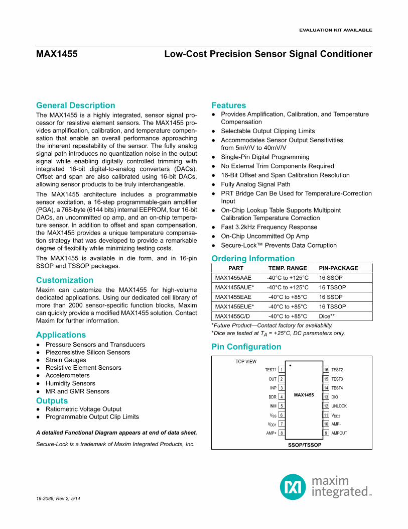
General Description The MAX1455 is a highly integrated, sensor signal pro- cessor for resistive element sensors. The MAX1455 pro- vides amplification, calibration, and temperature compen- sation that enable an overall performance approaching the inherent repeatability of the sensor. The fully analog signal path introduces no quantization noise in the output signal while enabling digitally controlled trimming with integrated 16-bit digital-to-analog converters (DACs). Offset and span are also calibrated using 16-bit DACs, allowing sensor products to be truly interchangeable. The MAX1455 architecture includes a programmable sensor excitation, a 16-step programmable-gain amplifier (PGA), a 768-byte (6144 bits) internal EEPROM, four 16-bit DACs, an uncommitted op amp, and an on-chip tempera- ture sensor. In addition to offset and span compensation, the MAX1455 provides a unique temperature compensa- tion strategy that was developed to provide a remarkable degree of flexibility while minimizing testing costs. The MAX1455 is available in die form, and in 16-pin SSOP and TSSOP packages. Customization Maxim can customize the MAX1455 for high-volume dedicated applications. Using our dedicated cell library of more than 2000 sensor-specific function blocks, Maxim can quickly provide a modified MAX1455 solution. Contact Maxim for further information. Applications ● Pressure Sensors and Transducers ● Piezoresistive Silicon Sensors ● Strain Gauges ● Resistive Element Sensors ● Accelerometers ● Humidity Sensors ● MR and GMR Sensors Outputs ● Ratiometric Voltage Output ● Programmable Output Clip Limits Features ● Provides Amplification, Calibration, and Temperature Compensation ● Selectable Output Clipping Limits ● Accommodates Sensor Output Sensitivities from 5mV/V to 40mV/V ● Single-Pin Digital Programming ● No External Trim Components Required ● 16-Bit Offset and Span Calibration Resolution ● Fully Analog Signal Path ● PRT Bridge Can Be Used for Temperature-Correction Input ● On-Chip Lookup Table Supports Multipoint Calibration Temperature Correction ● Fast 3.2kHz Frequency Response ● On-Chip Uncommitted Op Amp ● Secure-Lock™ Prevents Data Corruption A detailed Functional Diagram appears at end of data sheet. 19-2088; Rev 2; 5/14 *Future Product—Contact factory for availability. *Dice are tested at T A = +25°C, DC parameters only. Secure-Lock is a trademark of Maxim Integrated Products, Inc. PART TEMP. RANGE PIN-PACKAGE MAX1455AAE -40°C to +125°C 16 SSOP MAX1455AUE* -40°C to +125°C 16 TSSOP MAX1455EAE -40°C to +85°C 16 SSOP MAX1455EUE* -40°C to +85°C 16 TSSOP MAX1455C/D -40°C to +85°C Dice** 16 15 14 13 12 11 10 9 1 2 3 4 5 6 7 8 TEST1 TEST2 TEST3 TEST4 DIO UNLOCK V DD2 AMP- AMPOUT TOP VIEW MAX1455 SSOP/TSSOP OUT INP V SS BDR INM V DD1 AMP+ MAX1455 Low-Cost Precision Sensor Signal Conditioner Ordering Information Pin Configuration EVALUATION KIT AVAILABLE
Transcript
General DescriptionThe MAX1455 is a highly integrated, sensor signal pro-cessor for resistive element sensors. The MAX1455 pro-vides amplification, calibration, and temperature compen-sation that enable an overall performance approaching the inherent repeatability of the sensor. The fully analog signal path introduces no quantization noise in the output signal while enabling digitally controlled trimming with integrated 16-bit digital-to-analog converters (DACs). Offset and span are also calibrated using 16-bit DACs, allowing sensor products to be truly interchangeable. The MAX1455 architecture includes a programmable sensor excitation, a 16-step programmable-gain amplifier (PGA), a 768-byte (6144 bits) internal EEPROM, four 16-bit DACs, an uncommitted op amp, and an on-chip tempera-ture sensor. In addition to offset and span compensation, the MAX1455 provides a unique temperature compensa-tion strategy that was developed to provide a remarkable degree of flexibility while minimizing testing costs.The MAX1455 is available in die form, and in 16-pin SSOP and TSSOP packages.
CustomizationMaxim can customize the MAX1455 for high-volume dedicated applications. Using our dedicated cell library of more than 2000 sensor-specific function blocks, Maxim can quickly provide a modified MAX1455 solution. Contact Maxim for further information.
Applications Pressure Sensors and Transducers Piezoresistive Silicon Sensors Strain Gauges Resistive Element Sensors Accelerometers Humidity Sensors MR and GMR Sensors
Outputs Ratiometric Voltage Output Programmable Output Clip Limits
Features Provides Amplification, Calibration, and Temperature
from 5mV/V to 40mV/V Single-Pin Digital Programming No External Trim Components Required 16-Bit Offset and Span Calibration Resolution Fully Analog Signal Path PRT Bridge Can Be Used for Temperature-Correction
Input On-Chip Lookup Table Supports Multipoint
Calibration Temperature Correction Fast 3.2kHz Frequency Response On-Chip Uncommitted Op Amp Secure-Lock™ Prevents Data Corruption
A detailed Functional Diagram appears at end of data sheet.
19-2088; Rev 2; 5/14
*Future Product—Contact factory for availability.*Dice are tested at TA = +25°C, DC parameters only.
Secure-Lock is a trademark of Maxim Integrated Products, Inc.
PART TEMP. RANGE PIN-PACKAGEMAX1455AAE -40°C to +125°C 16 SSOP
MAX1455AUE* -40°C to +125°C 16 TSSOP
MAX1455EAE -40°C to +85°C 16 SSOP
MAX1455EUE* -40°C to +85°C 16 TSSOP
MAX1455C/D -40°C to +85°C Dice**
16
15
14
13
12
11
10
9
1
2
3
4
5
6
7
8
TEST1 TEST2
TEST3
TEST4
DIO
UNLOCK
VDD2
AMP-
AMPOUT
TOP VIEW
MAX1455
SSOP/TSSOP
OUT
INP
VSS
BDR
INM
VDD1
AMP+
MAX1455 Low-Cost Precision Sensor Signal Conditioner
Ordering Information
Pin Configuration
EVALUATION KIT AVAILABLE
Supply Voltage, VDD_ to VSS ..................................... -0.3V, +6VVDD1 - VDD2 ............................................................ -0.3V, +0.6VAll Other Pins .............................. (VSS - 0.3V) to (VDD_ + 0.3V)Short-Circuit Duration, OUT, BDR, AMPOUT ............ContinuousContinuous Power Dissipation (TA = +70°C)
Operating Temperature Ranges (TMIN to TMAX) MAX1455C/D .................................................. -40°C to +85°C MAX1455EAE ................................................. -40°C to +85°C MAX1455AAE ............................................... -40°C to +125°C
MAX1455EUE................................................. -40°C to +85°C MAX1455AUE............................................... -40°C to +125°C
Storage Temperature Range ............................ -65°C to +150°CLead Temperature (soldering, 10s) ................................ +300°C
PARAMETER SYMBOL CONDITIONS MIN TYP MAX UNITSGENERAL CHARACTERISTICSSupply Voltage VDD 4.5 5.0 5.5 V
Supply Current IDD IDD1 + IDD2 (Note 1) 3.0 6.0 mA
Oscillator Frequency fOSC 0.85 1 1.15 MHz
ANALOG INPUTInput Impedance RIN 1 MΩInput-Referred Adjustable Offset Range Offset TC = 0 (Note 2), minimum gain ±150 mV
Input-Referred Offset Tempco TA = TMIN to TMAX ±1 µV/°C
Amplifier Gain Nonlinearity 0.025 %
Common-Mode Rejection Ratio CMRR Specified for common-mode voltages between VSS and VDD
90 dB
Minimum Input-Referred FSO Range (Note 3) 7 mV/V
Maximum Input-Referred FSO Range (Note 3) 40 mV/V
ANALOG OUTPUTMinimum Differential Signal-Gain Range PGA [3:0] = 0000 39 V/V
Maximum Differential Signal-Gain Range PGA [3:0] = 1111 234 V/V
Output Clip Voltage Settings VOUTNo load, TA = TMIN to TMAX
Clip[1:0] = 00Low 0.10
V
High 4.90
Clip[1:0] = 01Low 0.15
High 4.85
Clip[1:0] = 10Low 0.20
High 4.80
Clip[1:0] = 11Low 0.25
High 4.75
Load Current Source VOUT = +0.5V to +4.5V, TA = TMIN to TMAX, Clip[1:0] = 00 1 mA
MAX1455 Low-Cost Precision Sensor Signal Conditioner
www.maximintegrated.com Maxim Integrated 2
Absolute Maximum Ratings
Stresses beyond those listed under “Absolute Maximum Ratings” may cause permanent damage to the device. These are stress ratings only, and functional operation of the device at these or any other conditions beyond those indicated in the operational sections of the specifications is not implied. Exposure to absolute maximum rating conditions for extended periods may affect device reliability.
Note 1: Excludes sensor or load current.Note 2: This is the maximum allowable sensor offset.Note 3: This is the sensor’s sensitivity normalized to its drive voltage, assuming a desired full-span output of 4V and a bridge volt-
age of 2.5V.Note 4: Bit weight is ratiometric to VDD.Note 5: All units production tested at TA = +25°C. Limits over temperature are guaranteed by design.Note 6: Programming of the EEPROM at temperatures below +70°C is recommended.Note 7: For operation above +70°C, limit erase/write cycle to 100.Note 8: All erase commands require 7.1ms minimum time.
MAX1455 Low-Cost Precision Sensor Signal Conditioner
www.maximintegrated.com Maxim Integrated 4
Electrical Characteristics (continued)
Typical Operating Characteristics
Detailed DescriptionThe MAX1455 provides amplification, calibration, and tem-perature compensation to enable an overall performance approaching the inherent repeatability of the sensor. The fully analog signal path introduces no quantization noise in the output signal while enabling digitally controlled trimming with the integrated 16-bit DACs. The MAX1455 includes four selectable high/low clipping limits set in dis-crete 50mV steps from 0.1V/4.9V to 0.25V/4.75V. Offset and span can be calibrated to within ±0.02% of span.The MAX1455 architecture includes a programmable sensor excitation, a 16-step PGA, a 768-byte (6144 bits) internal EEPROM, four 16-bit DACs, an uncommitted op amp, and an on-chip temperature sensor. The MAX1455 also provides a unique temperature compensation strat-egy that was developed to provide a remarkable degree of flexibility while minimizing testing costs.The customer can select from 1 to 114 temperature points to compensate their sensor. This allows the latitude to compensate a sensor with a simple first-order linear correction or match an unusual tempera-ture curve. Programming up to 114 independent 16-bit EEPROM locations corrects performance in 1.5°C tem-
perature increments over a range of -40°C to +125°C. For sensors that exhibit a characteristic temperature performance, a select number of calibration points can be used with a number of preset values that define the temperature curve. The sensor and the MAX1455 should be at the same temperature during calibration and use. This allows the electronics and sensor errors to be com-pensated together and optimizes performance. For appli-cations where the sensor and electronics are at different temperatures, the MAX1455 can use the sensor bridge as an input to correct for temperature errors.The single pin, serial DIO communication architecture and the ability to timeshare its activity with the sensor’s output signal enables output sensing and calibration programming on a single line by parallel connecting OUT and DIO. The MAX1455 provides a Secure-Lock feature that allows the customer to prevent modification of sen-sor coefficients and the 52-byte user-definable EEPROM data after the sensor has been calibrated. The Secure-Lock feature also provides a hardware override to enable factory rework and recalibration by assertion of logic high on the UNLOCK pin.
PIN NAME FUNCTION
1, 15, 16TEST1, TEST3, TEST2
Test Pins. Connect to VSS or leave unconnected.
2 OUT Analog Output. Internal voltage nodes can be accessed in digital mode. OUT can be parallel connected to DIO. Bypass OUT to ground with a 0.1µF capacitor to reduce output noise.
3 INP Positive Input. Can be swapped to INM by the Configuration register.
4 BDR Bridge Drive Output
5 INM Negative Input. Can be swapped to INP by the Configuration register.
6 VSS Negative Supply Voltage
7 VDD1 Positive Supply Voltage 1. Connect a 0.1µF capacitor from VDD to VSS.
8 AMP+ Auxiliary Op Amp Positive Input
9 AMPOUT Auxiliary Op Amp Output
10 AMP- Auxiliary Op Amp Negative Input
11 VDD2Positive Supply Voltage 2. Connect a 0.47µF capacitor from VDD2 to VSS. Connect VDD2 to VDD1 or for improved noise performance, connect a 1kΩ resistor to VDD1.
12 UNLOCK Secure-Lock Disable. There is a 150µA pulldown to VSS. Connect to VDD to disable Secure-Lock and enable serial communication.
13 DIO Digital Input Output. Single-pin serial communication port. There are no internal pullups on DIO. Connect pullup resistor from DIO to VDD when in digital mode.
14 TEST4 Test Pin. Do not connect.
MAX1455 Low-Cost Precision Sensor Signal Conditioner
www.maximintegrated.com Maxim Integrated 5
Pin Description
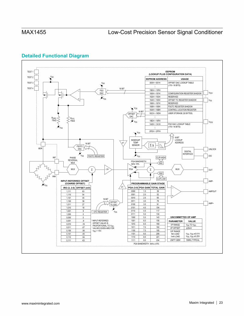
The MAX1455 allows complete calibration and sensor verification to be performed at a single test station. Once calibration coefficients have been stored in the ASIC, the customer can choose to retest in order to verify perfor-mance as part of a regular QA audit or to generate final test data on individual sensors. In addition, Maxim has developed a pilot production test system to reduce time to market. Engineering test evaluation and pilot produc-tion of the MAX1455 can be performed without expending the cost and time to develop in-house test capabilities. Contact Maxim for additional information.Frequency response can be user adjusted to values lower than the 3.2kHz bandwidth by using the uncommitted op amp and simple passive components.The MAX1455 (Figure 1) provides an analog amplification path for the sensor signal. It uses a digitally controlled analog path for nonlinear temperature correction. For PRT applications, analog architecture is available for first-order temperature correction. Calibration and correction are achieved by varying the offset and gain of a PGA and by varying the sensor bridge excitation current or voltage. The PGA utilizes a switched capacitor CMOS technology, with an input-referred offset trimming range of more than ±150mV with an approximate 3µV resolution (16 bits). The PGA provides gain values from 39V/V to 234V/V in 16 steps. The MAX1455 uses four 16-bit DACs with calibration coefficients stored by the user in an internal 768 x 8 EEPROM (6144 bits). This memory contains the following information, as 16-bit-wide words:• Configuration register• Offset calibration coefficient table• Offset temperature coefficient register• FSO calibration coefficient table• FSO temperature correction register• 52 bytes (416 bits) uncommitted for customer pro-
gramming of manufacturing data (e.g., serial number and date)
Offset CorrectionInitial offset correction is accomplished at the input stage of the signal gain amplifiers by a coarse offset setting. Final offset correction occurs through the use of a temper-ature-indexed lookup table with one hundred seventy-six 16-bit entries. The on-chip temperature sensor provides a unique 16-bit offset trim value from the table with an indexing resolution of approximately 1.5°C from -40°C
to +125°C. Every millisecond, the on-chip temperature sensor provides indexing into the offset lookup table in EEPROM and the resulting value is transferred to the offset DAC register. The resulting voltage is fed into a summing junction at the PGA output, compensating the sensor offset with a resolution of ±76µV (±0.0019% FSO). If the offset TC DAC is set to zero, then the maximum temperature error is equivalent to 1°C of temperature drift of the sensor, given that the Offset DAC has corrected the sensor every 1.5°C. The temperature indexing boundar-ies are outside the specified absolute maximum ratings. The minimum indexing value is 00hex, corresponding to approximately -69°C. All temperatures below this value output the coefficient value at index 00hex. The maximum indexing value is AFhex, which is the highest lookup table entry. All temperatures higher than approximately +184°C output the highest lookup table index value. No indexing wraparound errors are produced.
FSO CorrectionTwo functional blocks control the FSO gain calibration. First, a coarse gain is set by digitally selecting the gain of the PGA. Second, FSODAC sets the sensor bridge
Figure 1. Functional Diagram
MAX1455BIAS
GENERATOROSCILLATOR
ANAMUX
AMP-
AMPOUT
OUT
TEST 1
BDR
PGAINP
INM
8-BIT A/D
TEMPSENSOR
IRODAC
CURRENTSOURCE
CLIP-TOP
CLIP-BOT
TEST 2TEST 3TEST 4
AMP+
CONTROL
VDD1VDD2
DIOUNLOCK
VSS
176-POINTTEMPERATURE-
INDEXEDFSO
COEFFICIENTS
176-POINTTEMPERATURE-
INDEXEDOFFSET
COEFFICIENTS416 BITS FORUSER DATA
CONFIG REG6144-BITEEPROM
16-B
IT D
AC -
FSO
16-B
IT D
AC -
OFFS
ET16
-BIT
DAC
- OF
FSET
TC
16-B
IT D
AC -
FSO
TC
Σ
MAX1455 Low-Cost Precision Sensor Signal Conditioner
www.maximintegrated.com Maxim Integrated 6
current or voltage with the digital input obtained from a temperature indexed reference to the FSO lookup table in EEPROM. FSO correction occurs through the use of a temperature indexed lookup table with one hundred sev-enty-six 16-bit entries. The on-chip temperature sensor provides a unique FSO trim from the table with an index-ing resolution approaching one 16-bit value every 1.5°C from -40°C to +125°C. The temperature indexing bound-aries are outside the specified absolute maximum ratings. The minimum indexing value is 00hex, corresponding to approximately -69°C. All temperatures below this value output the coefficient value at index 00hex. The maximum indexing value is AFhex, which is the highest lookup table entry. All temperatures higher than approximately +184°C output the highest lookup table index value. No indexing wraparound errors are produced.
Linear and Nonlinear Temperature CompensationWriting 16-bit calibration coefficients into the offset TC and FSOTC registers compensates first-order tempera-ture errors. The piezoresistive sensor is powered by a current source resulting in a temperature-dependent bridge voltage due to the sensor’s temperature coefficient resistance (TCR). The reference inputs of the offset TC DAC and FSOTC DAC are connected to the bridge volt-age. The DAC output voltages track the bridge voltage as it varies with temperature, and by varying the offset TC and FSOTC digital code and a portion of the bridge voltage, which is temperature dependent, is used to com-pensate the first-order temperature errors.The internal feedback resistors (RISRC and RSTC) for FSO temperature compensation are set to 75kΩ.To calculate the required offset TC and FSOTC compen-sation coefficients, two test temperatures are needed. After taking at least two measurements at each tempera-ture, calibration software (in a host computer) calculates the correction coefficients and writes them to the internal EEPROM. With coefficients ranging from 0000hex to FFFFhex and a +5V reference, each DAC has a resolution of 76µV. Two of the DACs (offset TC and FSOTC) utilize the sensor bridge voltage as a reference. Since the sensor bridge voltage is approximately set to +2.5V, the FSOTC and offset TC exhibit a step size of less than 38µV. For high-accuracy applications (errors less than 0.25%), the first-order offset TC and FSOTC should be compensat-
ed with the offset TC and FSOTC DACs, and the residual higher order terms with the lookup table. The offset and FSO compensation DACs provide unique compensation values for approximately 1.5°C of temperature change as the temperature indexes the address pointer through the coefficient lookup table. Changing the offset does not affect the FSO; however, changing the FSO affects the offset due to the nature of the bridge. The temperature is measured on both the MAX1455 die and at the bridge sensor. It is recommended to compensate the first-order temperature errors using the bridge sensor temperature.
Typical Ratiometric Operating CircuitRatiometric output configuration provides an output that is proportional to the power-supply voltage. This output can then be applied to a ratiometric ADC to produce a digital value independent of supply voltage. Ratiometricity is an important consideration for battery-operated instruments, automotive, and some industrial applications.The MAX1455 provides a high-performance ratiometric output with a minimum number of external components (Figure 2). These external components include the fol-lowing:• One supply bypass capacitor• One optional output EMI suppression capacitor
Typical Nonratiometric Operating Circuit (5.5VDC < VPWR < 28VDC)Nonratiometric output configuration enables the sensor power to vary over a wide range. A low-dropout volt-age regulator, such as the MAX1615, is incorporated in the circuit to provide a stable supply and reference for MAX1455 operation. A typical example is shown in Figure 3. Nonratiometric operation is valuable when wide ranges of input voltage are to be expected and the system A/D or readout device does not enable ratiometric operation.
Internal Calibration RegistersThe MAX1455 has five 16-bit internal calibration registers (ICRs) that are loaded from EEPROM, or loaded from the serial digital interface.Data can be loaded into the ICRs under three different circumstances.Normal Operation, Power-On Initialization Sequence:• The MAX1455 has been calibrated, the Secure-Lock
byte is set (CL[7:0] = FFhex), and UNLOCK is low.
MAX1455 Low-Cost Precision Sensor Signal Conditioner
www.maximintegrated.com Maxim Integrated 7
• Power is applied to the device.• The power-on reset (POR) functions have been com-
pleted.• Registers CONFIG, OTCDAC, and FSOTCDAC are
refreshed from EEPROM.• Registers ODAC and FSODAC are refreshed from the
temperature indexed EEPROM locations.Normal Operation, Continuous Refresh:• The MAX1455 has been calibrated, the Secure-Lock byte
has been set (CL[7:0] = FFhex), and UNLOCK is low.
• Power is applied to the device.• The POR functions have been completed.• The temperature index timer reaches a 1ms time
period.• Registers CONFIG, OTCDAC, and FSOTCDAC are
refreshed from EEPROM.• Registers ODAC and FSODAC are refreshed from the
MAX1455 Low-Cost Precision Sensor Signal Conditioner
www.maximintegrated.com Maxim Integrated 8
Calibration Operation, Registers Updated by Serial Communications:• The MAX1455 has not had the Secure-Lock byte set
(CL[7:0] = 00hex) or UNLOCK is high.• Power is applied to the device.• The POR functions have been completed.• The registers can then be loaded from the serial digital
interface by use of serial commands. See the section on serial I/O and commands.
Internal EEPROMThe internal EEPROM is organized as a 768 by 8-bit memory. It is divided into 12 pages, with 64 bytes per page. Each page can be individually erased. The memory structure is arranged as shown in Table 1. The look-up tables for ODAC and FSODAC are also shown, with the respective temperature index pointer. Note that the ODAC table occupies a continuous segment, from address 000hex to address 15Fhex, whereas the FSODAC table is divided in two parts, from 200hex to 2FFhex, and from 1A0hex to 1FFhex. With the exception of the general-purpose user bytes, all values are 16-bit-wide words formed by two adjacent byte locations (high byte and low byte).The MAX1455 compensates for sensor offset, FSO, and temperature errors by loading the internal calibration registers with the compensation values. These compen-sation values can be loaded to registers directly through the serial digital interface during calibration or loaded automatically from EEPROM at power-on. In this way, the device can be tested and configured during calibration and test and the appropriate compensation values stored in internal EEPROM. The device autoloads the registers from EEPROM and is ready for use without further con-figuration after each power-up. The EEPROM is configured as an 8-bit-wide array so each of the 16-bit registers is stored as two 8-bit quantities. The Configuration register, FSOTCDAC, and OTCDAC registers are loaded from the preassigned locations in the EEPROM. Table 2 is the EEPROM ODAC and FSODAC lookup table memory map.The ODAC and FSODAC are loaded from the EEPROM lookup tables using an index pointer that is a function of temperature. An ADC converts the integrated temperature sensor to an 8-bit value every 1ms. This digitized value is then transferred into the temp-index register. Table 3 lists the registers.The typical transfer function for the temp-index is as fol-lows:
temp-index = 0.69 x Temperature (°C) + 47.58
where temp-index is truncated to an 8-bit integer value. Typical values for the temp-index register are given in Table 4.Note that the EEPROM is 1 byte wide and the registers that are loaded from EEPROM are 16 bits wide. Thus, each index value points to 2 bytes in the EEPROM.Maxim programs all EEPROM locations to FFhex with the exception of the oscillator frequency setting and Secure-Lock byte. OSC[2:0] is in the Configuration register (Table 5). These bits should be maintained at the factory-preset values. Programming 00hex in the Secure-Lock byte (CL[7:0] = 00hex) configures the DIO as an asynchronous serial input for calibration and test purposes.
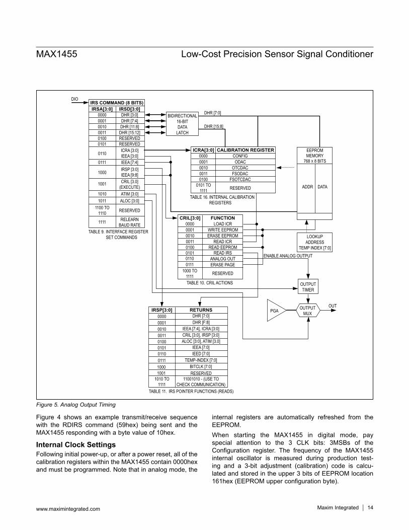
MAX1455 Digital ModeA single-pin serial interface provided by the DIO accesses the MAX1455’s control functions and memory. All com-mand inputs to this pin flow into a set of 16 registers, which form the interface register set (IRS). Additional lev-els of command processing are provided by control logic, which takes its inputs from the IRS. A bidirectional 16-bit latch buffers data to and from the 16-bit Calibration regis-ters and internal (8-bit-wide) EEPROM locations. Figure 5 shows the relationship between the various serial com-mands and the MAX1455 internal architecture.
Communication ProtocolThe DIO serial interface is used for asynchronous serial data communications between the MAX1455 and a host calibration test system or computer. The MAX1455 auto-matically detects the baud rate of the host computer when the host transmits the initialization sequence. Baud rates between 4800 and 38400 can be detected and used. The data format is always 1 start bit, 8 data bits, and 1 stop bit. The 8 data bits are transmitted LSB first, MSB last. A weak pullup resistor can be used to maintain logic 1 on the DIO pin while the MAX1455 is in digital mode. This is to prevent unintended 1 to 0 transitions on this pin, which would be interpreted as a communication start bit. Communications are only allowed when the Secure-Lock byte is disabled (i.e., CL[7:0] = 00HEX ) or UNLOCK is held high. Table 8 is the control location.
Initialization Sequence The first Command Byte sent to the MAX1455 after pow-er-up, or following receipt of the reinitialization command, is used by the MAX1455 to learn the communication baud rate. The initialization sequence is a 1-byte transmiss of 01 hex, as follows:
1 1 1 1 1 1 1 1 1 1 10 0 0 0 0 0 001
MAX1455 Low-Cost Precision Sensor Signal Conditioner
www.maximintegrated.com Maxim Integrated 9
The start bit, shown in bold above, initiates the baud rate synchronization. The 8 data bits 01hex (LSB first) follow this and then the stop bit, also shown in bold above. The MAX1455 uses this sequence to calculate the time inter-val for a 1-bit transmission as a multiple of the period of its internal oscillator. The resulting number of oscillator
clock cycles is then stored internally as an 8-bit number (BITCLK). Note that the device power supply should be stable for a minimum period of 1ms before the initializa-tion sequence is sent. This allows time for the POR func-tion to complete and DIO to be configured by the Secure-Lock byte or UNLOCK.
Table 1. EEPROM Memory Address Map
PAGE LOW-BYTE ADDRESS (hex)
HIGH-BYTE ADDRESS (hex)
TEMP-INDEX[7:0] (hex) CONTENTS
0000 001 00
ODACLookup Table
03E 03F 1F
1040 041 2007E 07F 3F
2080 081 400BE 0BF 5F
30C0 0C1 600FE 0FF 7F
4100 101 8013E 13F 9F
5
140 141 A015E 15F AF to FF160 161 Configuration162 163 Reserved164 165 OTCDAC166 167 Reserved168 169 FSOTCDAC16A 16B Control Location16C 16D
52 General-PurposeUser Bytes
17E 17F
6
180 18119E 19F1A0 1A1 80
FSODACLookup Table
1BE 1BF 8F
71C0 1C1 901FE 1FF AF to FF
8200 201 0023E 23F 1F
9240 241 2027E 27F 3F
A280 281 402BE 2BF 5F
B2C0 2C1 602FE 2FF 7F
MAX1455 Low-Cost Precision Sensor Signal Conditioner
www.maximintegrated.com Maxim Integrated 10
Reinitialization SequenceThe MAX1455 provides for reestablishing, or relearning, the baud rate. The reinitialization sequence is a 1-byte transmiss of FFhex, as follows:
1 1 1 1 1 1 1 1 1 1 10 1 1 1 1 1 111
When a serial reinitialization sequence is received, the receive logic resets itself to its power-up state and waits for the initialization sequence. The initialization sequence must follow the reinitialization sequence in order to rees-tablish the baud rate.
Table 2. EEPROM ODAC and FSODAC Lookup Table Memory Map
Table 3. Registers
Table 4. Temp-Index Typical Values
Figure 4. MAX1455 Serial Command Structure and Hardware Schematic
DATA
DIO
TRANSMIT RECEIVEHIGH-ZHIGH-Z TRANSMITHOST
RECEIVE TRANSMITHIGH-Z RECEIVE
1 1 1 1 1 1 000 11 0 10 0 00 0 0 0 0 0 01 11 1 1 1 1 1 1 1 1 1 1 1 1 11 1 11 X X X X
WEAK PULLUPREQUIRED
WEAK PULLUPREQUIRED
TEMP-INDEX[7:0] EEPROM ADDRESS ODAC LOW BYTE AND HIGH BYTE
EEPROM ADDRESS FSODAC LOW BYTE AND HIGH BYTE
00hex to
7Fhex
000hex and 001hex to
0FEhex and 0FFhex
200hex and 201hex to
2FEhex and 2FFhex
80hex to
AFhex
100hex and 101hex to
15Ehex and 15Fhex
1A0hex and 1A1hex to
1FEhex and 1FFhex
REGISTER DESCRIPTIONCONFIG Configuration register
ODAC Offset DAC register
OTCDAC Offset temperature coefficient DAC register
FSODAC Full-span output DAC register
FSOTCDAC Full-span output temperature coefficient DAC register
TEMPERATURE(°C)
TEMP-INDEX[7:0]DECIMAL HEXADECIMAL
-40 20 14
+25 65 41
+85 106 6A
+125 134 86
MAX1455 Low-Cost Precision Sensor Signal Conditioner
www.maximintegrated.com Maxim Integrated 11
Serial Interface Command FormatAll communication commands into the MAX1455 follow the format of a start bit, 8 command bits (command byte), and a stop bit. The Command Byte controls the contents of the IRS and comprises a 4-bit interface register set address
(IRSA) nibble and a 4-bit interface register set data (IRSD) nibble. The IRS Command Byte is structured as follows:
IRS[7:0] = IRSD[3:0], IRSA[3:0]All commands are transmitted LSB first. The first bit fol-lowing the start bit is IRSA[0] and the last bit before the stop is IRSD[3] as follows:
IRSA IRSD1 1 1 1 1 0 0 1 2 3 0 1 2 3 1 1 1 1 1 1
Half of the register contents of the IRS are used for data hold and steering information. Data writes to two locations within the IRS cause immediate action (command execu-tion). These locations are at addresses 9 and 15 and are the Command Register to Internal Logic (CRIL) and reini-tialize commands, respectively. Table 9 shows a full listing of IRS address decoding.Command sequences can be written to the MAX1455 as a continuous stream, i.e., start bit, command byte, stop bit, start bit, command byte, stop bit, etc. There are no delay requirements between commands while the MAX1455 is receiving data.
Command Register to Internal LogicA data write to the CRIL location (IRS address 9) causes immediate execution of the command associated with the 4-bit data nibble written. All EEPROM and Calibration register read and write, together with EEPROM erase, commands are handled through the CRIL location. CRIL is also used to enable the MAX1455 analog output and to place output data (serial digital output) on DIO. Table 10 shows a full listing of CRIL commands.
Table 5. Configuration Register (CONFIG[15:0])
Table 6. PGA Gain Setting (PGA[3:0])
FIELD NAME DESCRIPTION
15:13 OSC[2:0] Oscillator frequency setting. Factory preset; do not change.
1 ODAC Sign Logic 1 for positive offset DAC output. Logic 0 for negative offset DAC output.
0 OTCDAC Sign Logic 1 for positive offset TC DAC output. Logic 0 for negative offset TC DAC output.
PGA[3:0] PGA GAIN (V/V)
0000 39
0001 52
0010 65
0011 78
0100 91
0101 104
0110 117
0111 130
1000 143
1001 156
1010 169
1011 182
1100 195
1101 208
1110 221
1111 234
MAX1455 Low-Cost Precision Sensor Signal Conditioner
www.maximintegrated.com Maxim Integrated 12
Serial Digital Output DIO is configured as a digital output by writing a Read IRS (RDIRS) command (5 hex) to the CRIL location. On receipt of this command, the MAX1455 outputs a byte of data, the contents of which are determined by the IRS pointer (IRSP[3:0]) value at location IRSA[3:0] = 8hex. The data is output as a single byte, framed by a start bit and a stop bit. Table 11 lists the data returned for each IRSP address value.Once the RDIRS command has been sent, all connec-tions to DIO must be three-stated to allow the MAX1455 to drive the DIO line. Following receipt of the RDIRS com-mand, the MAX1455 drives DIO high after 1 byte time. The MAX1455 holds DIO high for a single bit time and then asserts a start bit (drives DIO low). The start bit is then followed by the data byte and a stop bit. Immediately following transmission of the stop bit, the MAX1455 three-states DIO, releasing the line. The MAX1455 is then ready to receive the next command sequence 1 byte time after release of DIO.
Note that there are time intervals before and after the MAX1455 sends the data byte when all devices on the DIO line are three-stated. It is recommended that a weak pullup resistor be applied to the DIO line during these time intervals to prevent unwanted transitions (Figure 4). In applications where DIO and analog output (OUT) are not connected, a pullup resistor should be permanently con-nected to DIO. If the MAX1455 DIO and analog outputs are connected, then do not load this common line during analog measurements. In this situation, perform the fol-lowing sequence:1) Connect a pullup resistor to the DIO/OUT line, prefer-
ably with a relay.2) Send the RDIRS command.3) Three-state the user connection (set to high imped-
ance).4) Receive data from the MAX1455.5) Activate the user connection (pull DIO/OUT line high).6) Release the pullup resistor.
Table 7. Input Referred Offset (IRO[2:0])
IRO SIGN, IRO[2:0] INPUT-REFERRED OFFSET CORRECTION AS % OF VDD
INPUT-REFERRED OFFSET, CORRECTION AT VDD = 5VDC IN mV
1,111 +1.25 +63
1,110 +1.08 +54
1,101 +0.90 +45
1,100 +0.72 +36
1,011 +0.54 +27
1,010 +0.36 +18
1,001 +0.18 +9
1,000 0 0
0,000 0 0
0,001 -0.18 -9
0,010 -0.36 -18
0,011 -0.54 -27
0,100 -0.72 -36
0,101 -0.90 -45
0,110 -1.08 -54
0,111 -1.25 -63
MAX1455 Low-Cost Precision Sensor Signal Conditioner
www.maximintegrated.com Maxim Integrated 13
Figure 4 shows an example transmit/receive sequence with the RDIRS command (59hex) being sent and the MAX1455 responding with a byte value of 10hex.
Internal Clock SettingsFollowing initial power-up, or after a power reset, all of the calibration registers within the MAX1455 contain 0000hex and must be programmed. Note that in analog mode, the
internal registers are automatically refreshed from the EEPROM. When starting the MAX1455 in digital mode, pay special attention to the 3 CLK bits: 3MSBs of the Configuration register. The frequency of the MAX1455 internal oscillator is measured during production test-ing and a 3-bit adjustment (calibration) code is calcu-lated and stored in the upper 3 bits of EEPROM location 161hex (EEPROM upper configuration byte).
MAX1455 Low-Cost Precision Sensor Signal Conditioner
www.maximintegrated.com Maxim Integrated 14
The MAX1455 internal clock controls timing functions, including the signal path gain, DAC functions, and com-munications. It is recommended that, while in digital mode, the Configuration register CLK bits be assigned the values contained in EEPROM (upper configuration byte). The 3 CLK bits represent a two’s-complement number with a nominal clock adjustment of 9% per bit. Table 12 shows the codes and adjustment available.Any change to the CLK bit values contained in the Configuration register must be followed by the MAX1455 baud rate learning sequence (reinitialize and initialize commands). To maximize the robustness of the commu-nication system during clock resetting only, change the CLK bits by 1 LSB value at a time. The recommended set-ting procedure for the Configuration register CLK bits is, therefore, as follows. (Use a minimum baud rate of 9600 during the setting procedure to prevent potential overflow of the MAX1455 baud rate counter with clock values near maximum.)
The following example is based on a required CLK code of 010 binary:1) Read the CLK bits (3MSBs) from EEPROM location
161hex. CLK = 010 binary.2) Set the CLK bits in the Configuration register to 001
binary.3) Send the reinitialize command, followed by the initial-
ize (baud rate learning) command.4) Set the CLK bits in the Configuration register to 010
binary.5) Send the reinitialize command, followed by the initialize
(baud rate learning) command.The frequency of the internal oscillator can be checked at any time by reading the value of BITCLK[7:0]. This 8-bit number represents the number of internal oscillator cycles corresponding to 1 cycle (1 bit time) of the communica-tions baud rate.
Table 8. Control Location (CL[15:0])
Table 9. IRSA Decoding
FIELD NAME DESCRIPTION15:8 CL[15:8] Reserved
7:0 CL[7:0] Control Location. Secure-Lock is activated by setting this to FFhex, which disables DIO serial communications and connects OUT to PGA output.
IRSA[3:0] DESCRIPTION0000 Write IRSD[3:0] to DHR[3:0] (Data Hold register)
0001 Write IRSD[3:0] to DHR[7:4] (Data Hold register)
0010 Write IRSD[3:0] to DHR[11:8] (Data Hold register)
0011 Write IRSD[3:0] to DHR[15:12] (Data Hold register)
0100 Reserved
0101 Reserved
0110 Write IRSD[3:0] to ICRA[3:0] or IEEA[3:0] (Internal Calibration register address or internal EEPROM address nibble 0)
0111 Write IRSD[3:0] to IEEA[7:4] (internal EEPROM address, nibble 1)
1000 Write IRSD[3:0] to IRSP[3:0] or IEEA[9:8] (Interface register set pointer where IRSP[1:0] is IEEA[9:8])
1001 Write IRSD[3:0] to CRIL[3:0] (Command register to internal logic)
1010 Write IRSD[3:0] to ATIM[3:0] (analog timeout value on read)
1011 Write IRSD[3:0] to ALOC[3:0] (analog location)
1100 to 1110 Reserved
1111 Write IRSD[3:0] = 1111bin to relearn the baud rate
MAX1455 Low-Cost Precision Sensor Signal Conditioner
www.maximintegrated.com Maxim Integrated 15
Erasing and Writing to the EEPROMThe internal EEPROM must be erased (bytes set to FFhex) prior to programming the desired contents. The MAX1455 is supplied in a nominally erased state except byte 161hex and byte 16Bhex. The 3MSBs of byte 161hex contain the internal oscillator calibration setting. Byte 16Bhex is set to 00hex to allow serial communication regardless of the UNLOCK status. When erasing the EEPROM, first save the 3MSBs of byte 161hex. Following erasure, these 3 bits must be rewrit-ten, together with the Secure-Lock byte value of 00hex. Failure to do this may cause the part to stop communi-cating. Do not remove power from the device before rewriting these values.The internal EEPROM can be entirely erased with the ERASE command or partially erased with the PageErase command (Table 10). It is necessary to wait 7.1ms after issuing an erase or PageErase command. Any attempt to communicate with the part or to interrupt power before 7.1ms have elapsed may produce indeterminate states within the EEPROM.To erase a page in EEPROM (PageErase command): First load the required page number (Table 1) into the IRS location IEEA[3:0]. Then send a CRIL PageErase command (79hex).To write a byte to EEPROM: Load IRS locations IEEA[9:8], IEEA[7:4], and IEEA[3:0] with the byte address (Address[9:0]). Load IRS locations DHR[7:4] and DHR[3:0]
with the 8 data bits to be written (Data[7:0]). Send the EEPROM WRITE command to CRIL (19hex).To read a byte from EEPROM: 1) Load IRS locations IEEA[9:8], IEEA[7:4], and IEEA[3:0]
with the byte address (Address[9:0]). 2) Send a READ EEPROM command to the CRIL regis-
ter (49hex); this loads the required EEPROM byte into DHR[7:0].
3) Load IRS location IRSP[3:0] with 00hex (return DHR[7:0]).
4) Send the READ IRSP command to the CRIL register (59hex).
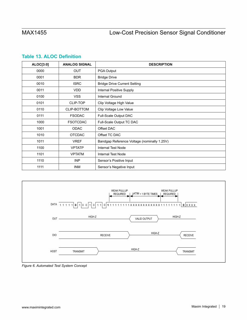
Multiplexed Analog OutputThe MAX1455 provides the facility to output analog signals while in digital mode through the read analog (RdAlg) com-mand. One byte time after receiving the RdAlg command, the internal analog signal determined by the ALOC[3:0] register (Table 13) is multiplexed to the MAX1455 OUT. The signal remains connected to OUT for the duration set by the ATIM[3:0] register. The ATIM function uses the com-munication baud rate as a timing basis. See Table 14 for details. At the end of the period determined by ATIM[3:0], the analog signal is disconnected from the analog output and OUT resumes a three-state condition. The MAX1455 can receive further commands on DIO 1 byte after resum-ing a three-state condition on OUT. Figure 6 shows the timing of this scheme.
Table 10. CRIL Command CodesCRIL[3:0] NAME DESCRIPTION
0000 LdICR Load Internal Calibration register at address given in ICRA with data from DHR[15:0].
0001 EEPW EEPROM write of 8 data bits from DHR[7:0] to address location pointed by IEEA [9:0].
0010 ERASE Erase all of EEPROM (all bytes equal FFhex).
0011 RdICR Read Internal Calibration register as pointed to by ICRA and load data into DHR[15:0].
0100 RdEEP Read internal EEPROM location and load data into DHR[7:0] pointed by IEEA [9:0].
0101 RdIRS Read Interface register set pointer IRSP[3:0]. See Table 11.
0110 RdAlgOutput the multiplexed analog signal onto OUT. The analog location is specified in ALOC[3:0] (Table 13) and the duration (in byte times) that the signal is asserted onto the pin is specified in ATIM[3:0] (Table 14).
0111 PageErase Erases the page of the EEPROM as pointed by IEEA[9:6]. There are 64 bytes per page and thus 12 pages in the EEPROM.
1000 to 1111 Reserved Reserved.
MAX1455 Low-Cost Precision Sensor Signal Conditioner
www.maximintegrated.com Maxim Integrated 16
The MAX1455 DIO is three-state for the duration that the analog output is active. This is to allow OUT and DIO to be connected in parallel. When DIO and OUT are con-nected in parallel, the host computer must also three-state its communications connection to the MAX1455. This requirement produces periods when all connections to the DIO are three-stated simultaneously, making it necessary to have a weak pullup resistor applied to DIO during these periods. A continuous output mode is available for the analog output and is selected by setting ATIM[3:0] to Fhex. This mode may only be used when DIO and OUT are separate. While in this mode and following receipt of the RdAlg command, or any other command, DIO three-states for a period of 32,769 byte times. Once this period has elapsed, DIO enters receive mode and accepts fur-ther command inputs. The analog output is always active while in continuous mode.Note: The internal analog signals are not buffered when connected to OUT. Any loading of OUT while one of these internal signals is being measured is likely to produce measurement errors. Do not load OUT when reading internal signals such as BDR, FSOTC, etc.
Table 11. IRSP Decode
Table 12. CLK Code (3MSBs of Configuration Register)
IRSP[3:0] RETURNED VALUE0000 DHR[7:0]
0001 DHR[15:8]
0010 IEEA[7:4], ICRA[3:0] concatenated
0011 CRIL[3:0], IRSP[3:0] concatenated
0100 ALOC[3:0], ATIM[3:0] concatenated
0101 IEEA[7:0] EEPROM address byte
0110 IEED[7:0] EEPROM data byte
0111 Temp-Index[7:0]
1000 BitClock[7:0]
1001 Reserved. Internal flash test data.
1010-1111 11001010 (CAhex). This can be used to test communication.
CLK CODE (BIN) CLOCK ADJUSTMENT (%)011 +27
010 +18
001 +9
000 0
111 -9
110 -18
101 -27
MAX1455 Low-Cost Precision Sensor Signal Conditioner
www.maximintegrated.com Maxim Integrated 17
Communication Command ExamplesA selection of examples of the command sequences for various functions within the MAX1455 follows.Example 1. Change the baud rate setting and check com-munications. If the communication with the MAX1455 is lost due to a system baud rate change before sending the reinitialization command, apply a power reset to guaran-tee the initialization condition:
Example 2. Read the lookup table pointer (Temp-Index):
Example 3. Enable BDR measurement on OUT pin for 3.4s duration with 9600 baud rate:
Example 4. Write 8C40hex to the FSODAC register:
Example 5. Write 8C40hex to the FSODAC lookup table location at Temp-Index 40. This example uses the page erase command to clear the relevant section of the EEPROM and assumes that none of the existing data in that section is required to be kept:
COMMAND ACTIONFFhex Reinitialize part ready for baud rate learning.
Change system baud rate to new value.
01hex Learn baud rate.
F8hex Load 15 (Fhex) to IRSP[3:0] register.
59hex Read IRS.
Host computer must be ready to receive data on the serial line within 1 (baud rate) byte time of sending the Read IRS command. The MAX1455 returns CAhex. (IRSP values of 10 to 15 are configured to return CAhex for communication checking purposes.)
COMMAND ACTION78hex Load 7 to IRSP[3:0] register.
59hex Read IRS.
Host ready to receive data within 1 byte time of sending the Read IRS command. The MAX1455 returns the current Temp-Index pointer value.
COMMAND ACTION
1Bhex Load 1 (BDR measurement) to ALOC[3:0] register.
CAhex Load 12 to the ATIM[3:0] register: (212+1) 5 8/9600 = 3.4s.
69hex RdAlg.
The DIO pin is three-stated and the OUT pin is connected internally to the BDR pin for a duration of approximately 3.4s.
COMMAND ACTION00hex Load 0 hex to the DHR[3:0] register.
41hex Load 4 hex to the DHR[7:4] register.
C2hex Load C hex to the DHR[11:8] register.
83hex Load 8 hex to the DHR[15:12] register.
36hex Load 3 (FSODAC) to the ICRA[3:0] register.
09hex Ld ICR.
8C40 hex is written to the FSODAC register.
COMMAND ACTION
A6hexLoad Ahex (page number corresponding to EEPROM locations 280hex and 281hex) to the IEEA[3:0] register.
79hex Page Erase command.
Wait 7.1ms before sending any further commands.
06hex Load 0hex to the IEEA[3:0] register.
87hex Load 8hex to the IEEA[7:4] register.
28hex Load 2hex to the IEEA[9:8] (IRSP[3:0]) register.
00hex Load 0hex to the DHR[3:0] register.
41hex Load 4hex to the DHR[7:4] register.
19hex
Write EEPROM. 40hex is loaded to EEPROM address 280hex, which is the low byte location corresponding to a Temp-Index pointer value of 40.
16hexLoad 1 to the IEEA[3:0] register. IEEA[7:4] and IEEA[9:8] already contain 8 and 2, respectively.
C0hex Load Chex to the DHR[3:0] register.
81hex Load 8hex to the DHR[7:4] register.
19hex
Write EEPROM. 8Chex is loaded to EEPROM address 281hex, which is the high byte location corresponding to a Temp-Index pointer value of 40.
MAX1455 Low-Cost Precision Sensor Signal Conditioner
www.maximintegrated.com Maxim Integrated 18
Table 13. ALOC Definition
Figure 6. Automated Test System Concept
WEAK PULLUPREQUIRED
1 1 1 1 1 0 1 0 0 1 0 1 0 1 1 1 1 1 1 1 1 X 1 1 1 1 1 1 1X XX X X XX X X1 X X 1 0
2ATIM + 1 BYTE TIMES
DATA
OUT VALID OUTPUTHIGH-Z
1 X X X X
WEAK PULLUPREQUIRED
HIGH-Z
RECEIVE RECEIVEHIGH-ZDIO
TRANSMITHIGH-Z
TRANSMITHOST
ALOC[3:0] ANALOG SIGNAL DESCRIPTION
0000 OUT PGA Output
0001 BDR Bridge Drive
0010 ISRC Bridge Drive Current Setting
0011 VDD Internal Positive Supply
0100 VSS Internal Ground
0101 CLIP-TOP Clip Voltage High Value
0110 CLIP-BOTTOM Clip Voltage Low Value
0111 FSODAC Full-Scale Output DAC
1000 FSOTCDAC Full-Scale Output TC DAC
1001 ODAC Offset DAC
1010 OTCDAC Offset TC DAC
1011 VREF Bandgap Reference Voltage (nominally 1.25V)
1100 VPTATP Internal Test Node
1101 VPTATM Internal Test Node
1110 INP Sensor’s Positive Input
1111 INM Sensor’s Negative Input
MAX1455 Low-Cost Precision Sensor Signal Conditioner
www.maximintegrated.com Maxim Integrated 19
Sensor Compensation OverviewCompensation requires an examination of the sensor per-formance over the operating pressure and temperature range. Use a minimum of two test pressures (e.g., zero and full span) and two temperatures. More test pressures and temperatures result in greater accuracy. A typical compensation procedure can be summarized as follows:
Set Reference Temperature (e.g., 25°C):• Initialize each transducer by loading its respective
register with default coefficients (e.g., based on mean
values of offset, FSO, and bridge resistance) to pre-vent overload of the MAX1455.
• Set the initial bridge voltage (with the FSODAC) to half of the supply voltage. Measure the bridge volt-age using the BDR or OUT pins, or calculate based on measurements.
• Calibrate the output offset and FSO of the transducer using the ODAC and FSODAC, respectively.
• Store calibration data in the test computer or MAX1455 EEPROM user memory.
Table 14. ATIM Definition
Table 15. IRCA Decode
ATIM[3:0] DURATION OF ANALOG SIGNAL SPECIFIED IN BYTE TIMES (8-BIT TIME)
1111 In this mode, OUT is continuous; however, DIO accepts commands after 32,769 byte times. Do not parallel connect DIO to OUT.
ICRA[3:0] NAME DESCRIPTION 0000 CONFIG Configuration register
0001 ODAC Offset DAC register
0010 OTCDAC Offset temperature coefficient DAC register
0011 FSODAC Full-scale output DAC register
0100 FSOTCDAC Full-scale output temperature coefficient DAC register
0101 Reserved. Do not write to this location (EEPROM test).0110 to
1111 Reserved. Do not write to this location.
MAX1455 Low-Cost Precision Sensor Signal Conditioner
www.maximintegrated.com Maxim Integrated 20
Set Next Test Temperature:• Calibrate offset and FSO using the ODAC and
FSODAC, respectively.• Store calibration data in the test computer or
MAX1455 EEPROM user memory.• Calculate the correction coefficients.• Download correction coefficients to EEPROM.• Perform a final test.
Sensor Calibration and Compensation ExampleThe MAX1455 temperature compensation design cor-rects both sensor and IC temperature errors. This enables the MAX1455 to provide temperature compensation approaching the inherent repeatability of the sensor. An example of the MAX1455’s capabilities is shown in Figure 8. Table 16 lists the effects of compensation.A MAX1455 and a repeatable piezoresistive sensor with an initial offset of 16.4mV and a span of 55.8mV were converted into a compensated transducer with an offset of
Figure 7. Comparison of an Uncalibrated Sensor and a Calibrated Transducer
Offset .....................................................................±100% FSOFSO ..............................................................1mV/V to 40mV/VOffset TC ...................................................................20% FSOOffset TC Nonlinearity .................................................4% FSOFSOTC .....................................................................-20% FSOFSOTC Nonlinearity ....................................................5% FSOTemperature Range ........................................ -40°C to +125°C
OUT .................................................Ratiometric to VDD at 5.0VOffset at +25°C .................................................0.500V ±200µVFSO at +25°C ...................................................4.000V ±200µVOffset Accuracy over Temp. Range ........... ±4mV (±0.1% FSO)FSO Accuracy over Temp. Range ............. ±4mV (±0.1% FSO)
MAX1455
VOUT
VDD
MODULE 1
DATA DATA
VSS VSS VDDVDD VSS
TEST OVEN
MAX1455
VOUT
MODULE 2
VOUT
DIGITALMULTIPLEXER
+5V
DIO[1:N]
DIO1 DIO2 DION
MAX1455
VOUT
MODULE N
DVM
MAX1455 Low-Cost Precision Sensor Signal Conditioner
www.maximintegrated.com Maxim Integrated 21
0.5000V and a span of 4.0000V. Nonlinear sensor offset and FSO temperature errors, which were on the order of 20% to 30% FSO, were reduced to under ±0.1% FSO. Figure 8 shows the output of the uncompensated sensor and the output of the compensated transducer. Six tem-perature points were used to obtain this result.• Store calibration data in the test computer or MAX1455
EEPROM user memory.
MAX1455 Evaluation KitTo expedite the development of MAX1455-based trans-ducers and test systems, Maxim has produced the MAX1455 evaluation kit (EV kit). First-time users of the MAX1455 are strongly encouraged to use this kit.The EV kit is designed to facilitate manual programming of the MAX1455 with a sensor. It includes the following: 1) Evaluation board with or without a silicon pressure
sensor, ready for customer evaluation.
2) Design/applications manual. This manual was devel-oped for test engineers familiar with data acquisition of sensor data and provides sensor compensation algo-rithms and test procedures.
3) MAX1455 communication software, which enables programming of the MAX1455 from a computer key-board (IBM compatible), one module at a time.
4) Interface adapter, which allows the connection of the evaluation board to a PC serial port.
Figure 8. Comparison of an Uncalibrated Sensor and a Calibrated Transducer
80
60
0
20
40
0 4020 60 80 100
RAW SENSOR OUTPUT(TA = +25°C)
PRESSURE (kps)
V OUT
(mV)
01
32
4
5
0 4020 60 80 100
COMPENSATED TRANSDUCER(TA = +25°C)
PRESSURE (kps)
V OUT
(V)
-20
10
3020
-10
0
UNCOMPENSATED SENSORTEMPERATURE ERROR
TEMPERATURE (°C)
ERRO
R (%
FSO
)
-50 500 100 150
FSO OFFSET
-0.15
-0.05-0.10
0.050
0.100.15
-50 500 100 150
COMPENSATED TRANSDUCER ERROR
TEMPERATURE (°C)
ERRO
R (%
FSO
)
FSO OFFSET
MAX1455 Low-Cost Precision Sensor Signal Conditioner
www.maximintegrated.com Maxim Integrated 22
Chip InformationPROCESS: CMOSSUBSTRATE CONNECTED TO: VSS
MAX1455 Low-Cost Precision Sensor Signal Conditioner
www.maximintegrated.com Maxim Integrated 24
Package InformationFor the latest package outline information and land patterns (footprints), go to www.maximintegrated.com/packages. Note that a “+”, “#”, or “-” in the package code indicates RoHS status only. Package drawings may show a different suffix character, but the drawing pertains to the package regardless of RoHS status.
1 10/01 Added TSSOP package to data sheet. 1, 2, 24
2 5/14 Updated General Description 1
Maxim Integrated cannot assume responsibility for use of any circuitry other than circuitry entirely embodied in a Maxim Integrated product. No circuit patent licenses are implied. Maxim Integrated reserves the right to change the circuitry and specifications without notice at any time. The parametric values (min and max limits) shown in the Electrical Characteristics table are guaranteed. Other parametric values quoted in this data sheet are provided for guidance.
Maxim Integrated and the Maxim Integrated logo are trademarks of Maxim Integrated Products, Inc.
MAX1455 Low-Cost Precision Sensor Signal Conditioner
For pricing, delivery, and ordering information, please contact Maxim Direct at 1-888-629-4642, or visit Maxim Integrated’s website at www.maximintegrated.com.