+5.0V, ±30kV ESD-Protected, Fail-Safe, Hot-Swap, RS-485/RS-422 Transceiver MAX14780E 19-5652; Rev 3; 1/15 General Description The MAX14780E is a +5V, ±30kV HBM ESD half duplex RS-485/422 transceiver. The MAX14780E features reduced slew-rate drivers that minimize EMI and reduce reflections caused by improp- erly terminated cables, allowing error-free data transmis- sion up to 500kbps. The MAX14780E is available in an 8-pin SO and PDIP packages operating over a temperature range from -40°C to +85°C. Applications Utility Meters Lighting Systems Industrial Control Telecom Security Systems Instrumentation Benefits and Features Integrated Protection Increases Robustness S ±30kV HBM ESD per JEDEC JS-001-2012 S ±12kV Contact ESD per IEC 61000-4-2 S ±15kV Air Gap ESD per IEC 61000-4-2 S True Fail-Safe Receiver Prevents False Transitions on Receiver Input Short or Open S Hot Swap Eliminates False Transitions During Power-Up or Hot Insertion S Short-Circuit Protected Outputs Low Current Reduces Power Consumption Low Current Reduces Power Consumption S 10µA Shutdown Current S 1.2mA of Supply Current When Unloaded Ordering Information +Denotes a lead(Pb)-free/RoHS-compliant package. Typical Operating Circuit Rt Rt DE RE A B A B 0.1μF TYPICAL HALF-DUPLEX OPERATING CIRCUIT + R D RO DI VCC GND 8 7 6 5 1 2 3 4 RE DE D R DI RO MAX14780E PART TEMP RANGE PIN-PACKAGE MAX14780EESA+ -40NC to +85NC 8 SO MAX14780EEPA+ -40NC to +85NC 8 PDIP For pricing, delivery, and ordering information, please contact Maxim Direct at 1-888-629-4642, or visit Maxim’s website at www.maximintegrated.com.
General DescriptionThe MAX14780E is a +5V, ±30kV HBM ESD half duplex RS-485/422 transceiver.
The MAX14780E features reduced slew-rate drivers that minimize EMI and reduce reflections caused by improp-erly terminated cables, allowing error-free data transmis-sion up to 500kbps.
The MAX14780E is available in an 8-pin SO and PDIP packages operating over a temperature range from -40°C to +85°C.
ApplicationsUtility Meters
Lighting Systems
Industrial Control
Telecom
Security Systems
Instrumentation
Benefits and FeaturesIntegrated Protection Increases RobustnessS ±30kV HBM ESD per JEDEC JS-001-2012S ±12kV Contact ESD per IEC 61000-4-2S ±15kV Air Gap ESD per IEC 61000-4-2S True Fail-Safe Receiver Prevents False
Transitions on Receiver Input Short or OpenS Hot Swap Eliminates False Transitions During
Power-Up or Hot InsertionS Short-Circuit Protected Outputs Low Current
Reduces Power Consumption
Low Current Reduces Power ConsumptionS 10µA Shutdown CurrentS 1.2mA of Supply Current When Unloaded
Ordering Information
+Denotes a lead(Pb)-free/RoHS-compliant package.
Typical Operating Circuit
RtRt
DE
RE
A
B
A
B
0.1µF
TYPICAL HALF-DUPLEX OPERATING CIRCUIT
+
R
D
RO
DI
VCC
GND
8
7
6
5
1
2
3
4
RE
DE
D
R
DI
RO
MAX14780E
PART TEMP RANGE PIN-PACKAGE
MAX14780EESA+ -40NC to +85NC 8 SO
MAX14780EEPA+ -40NC to +85NC 8 PDIP
For pricing, delivery, and ordering information, please contact Maxim Direct at 1-888-629-4642, or visit Maxim’s website at www.maximintegrated.com.
Stresses beyond those listed under “Absolute Maximum Ratings” may cause permanent damage to the device. These are stress ratings only, and functional operation of the device at these or any other conditions beyond those indicated in the operational sections of the specifications is not implied. Exposure to absolute maximum rating conditions for extended periods may affect device reliability.
(All voltages referenced to GND.)Supply Voltage (VCC) ........................................................... +6VControl Input Voltage (RE, DE) ...............................-0.3V to +6VDriver Input Voltage (DI) .........................................-0.3V to +6VDriver Output Voltage (A, B) ....................................-8V to +13VReceiver Input Voltage (A, B) ..................................-8V to +13VReceiver Output Voltage (RO) ................. -0.3V to (VCC + 0.3V)Driver Output Current .................................................... ±250mA
Continuous Power Dissipation (TA = +70°C) SO (derate 5.9mW/°C above +70°C) ..........................471mW PDIP (derate 9.1mW/°C above +70°C) .....................727.3mWOperating Temperature Range .......................... -40°C to +85°CJunction Temperature .....................................................+150°CStorage Temperature Range ............................ -65°C to +150°CLead Temperature (soldering, 10s) ................................+300°CSoldering Temperature (reflow) ......................................+260°C
DC ELECTRICAL CHARACTERISTICS(VCC = +5.0V ±10%, TA = TMIN to TMAX, unless otherwise noted. Typical values are at VCC = +5.0V and TA = +25NC.) (Note 1)
ABSOLUTE MAXIMUM RATINGS
PARAMETER SYMBOL CONDITIONS MIN TYP MAX UNITS
DRIVER
VCC Supply-Voltage Range VCC 4.5 5.5 V
Differential Driver Output VOD
RL = 100I (RS-422), Figure 1 3 VCC
VRL = 54I (RS-485), Figure 1 2 VCC
No load VCC
Change in Magnitude of Differential Output Voltage
DVOD RL = 100I or 54I, Figure 1 (Note 2) 0.2 V
Driver Common-Mode Output Voltage
VOC RL = 100I or 54I, Figure 1 VCC/2 3 V
Change in Magnitude of Common-Mode Voltage
DVOC RL = 100I or 54I, Figure 1 (Note 2) 0.2 V
Input-High Voltage VIH DE, DI, RE 3 V
Input-Low Voltage VIL DE, DI, RE 0.8 V
Input Hysteresis VHYS DE, DI, RE 100 mV
Input Current IIN1 DE, DI, RE Q1 FA
Input Impedance First Transition at Power-Up
RPWUP DE, RE = RE = 2V 3.65 8.8 kI
Input Impedance on First Transition after POR Delay
Rft DE = RE = 2V 7 60 kΩ
Driver Short-Circuit Output Current
IOSD0 P VOUT P +12V (Note 3) 40 250
mA-7V P VOUT P VCC (Note 3) -250 -40
Driver Short-Circuit Foldback Output Current
IOSDF(VCC - 1V) P VOUT P +12V (Note 3) 20
mA-7V P VOUT P +1V (Note 3) -20
Thermal-Shutdown Threshold TTS 175 NC
Thermal-Shutdown Hysteresis TTSH 15 NC
Input Current (A and B) IA, BVDE = 0V,VCC = 0V or VCC
DC ELECTRICAL CHARACTERISTICS (continued)(VCC = +5.0V ±10%, TA = TMIN to TMAX, unless otherwise noted. Typical values are at VCC = +5.0V and TA = +25NC.) (Note 1)
DRIVER SWITCHING CHARACTERISTICS WITH INTERNAL SRL (500kbps)(VCC = +5.0V ±10%, TA = TMIN to TMAX, unless otherwise noted. Typical values are at VCC = +5.0V and TA = +25NC.) (Note 1)
PARAMETER SYMBOL CONDITIONS MIN TYP MAX UNITS
RO Output-High Voltage VOH IO = -1mAVCC -
0.6V
RO Output-Low Voltage VOL IO = 1mA 0.4 V
Three-State Output Current at Receiver
IOZR 0 P VO P VCC P 1 FA
Receiver Input Resistance RIN -7V P VCM P +12V 96 kI
Note 1: All currents into the device are positive. All currents out of the device are negative. All voltages are referred to device ground, unless otherwise noted.
Note 2: ΔVOD and ΔVOC are the changes in VOD and VOC, respectively, when the DI input changes state.Note 3: The short-circuit output current applies to peak current just prior to foldback current limiting. The short-circuit foldback
output current applies during current limiting to allow a recovery from bus contention.
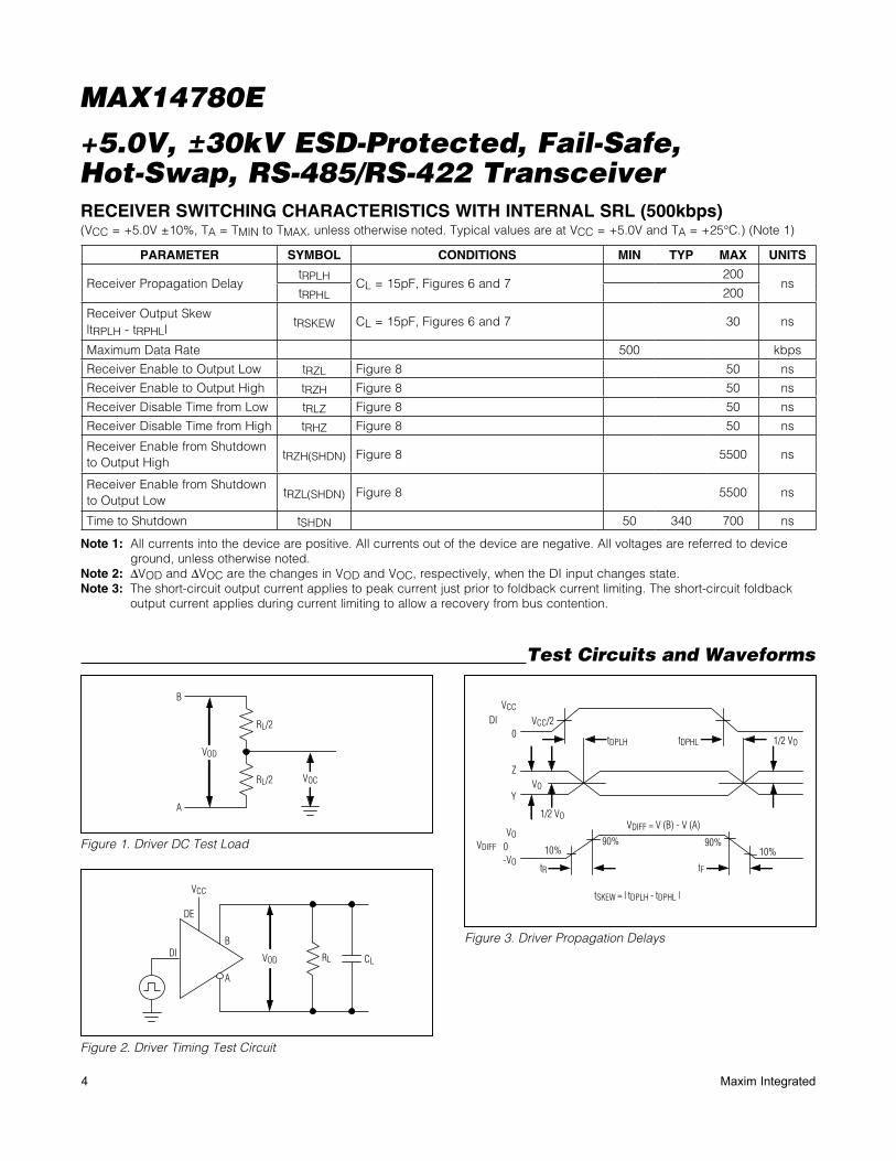
RECEIVER SWITCHING CHARACTERISTICS WITH INTERNAL SRL (500kbps)(VCC = +5.0V ±10%, TA = TMIN to TMAX, unless otherwise noted. Typical values are at VCC = +5.0V and TA = +25NC.) (Note 1)
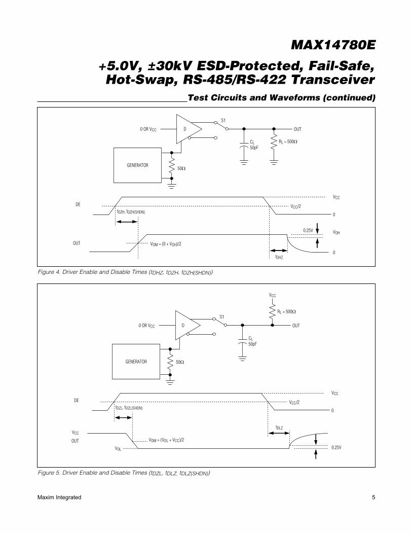
Test Circuits and Waveforms
Figure 1. Driver DC Test Load
Figure 2. Driver Timing Test Circuit
Figure 3. Driver Propagation Delays
B
A
VOD
VOC
RL/2
RL/2
DI
DE
VCC
A
B
VOD RL CL
DI
VCC
0
Z
Y
VO
0-VO
VO
VCC/2
tDPLH tDPHL
1/2 VO
10%
tR
90% 90%
1/2 VO
10%
tF
VDIFF = V (B) - V (A)
VDIFF
tSKEW = | tDPLH - tDPHL |
PARAMETER SYMBOL CONDITIONS MIN TYP MAX UNITS
Receiver Propagation DelaytRPLH
CL = 15pF, Figures 6 and 7200
nstRPHL 200
Receiver Output Skew|tRPLH - tRPHL|
tRSKEW CL = 15pF, Figures 6 and 7 30 ns
Maximum Data Rate 500 kbps
Receiver Enable to Output Low tRZL Figure 8 50 ns
Receiver Enable to Output High tRZH Figure 8 50 ns
Receiver Disable Time from Low tRLZ Figure 8 50 ns
Receiver Disable Time from High tRHZ Figure 8 50 ns
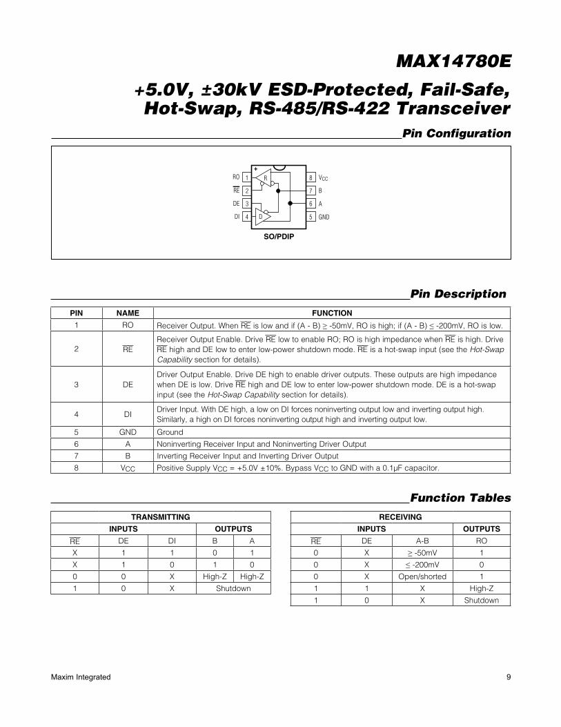
1 RO Receiver Output. When RE is low and if (A - B) R -50mV, RO is high; if (A - B) P -200mV, RO is low.
2 REReceiver Output Enable. Drive RE low to enable RO; RO is high impedance when RE is high. Drive RE high and DE low to enter low-power shutdown mode. RE is a hot-swap input (see the Hot-Swap Capability section for details).
3 DEDriver Output Enable. Drive DE high to enable driver outputs. These outputs are high impedance when DE is low. Drive RE high and DE low to enter low-power shutdown mode. DE is a hot-swap input (see the Hot-Swap Capability section for details).
4 DIDriver Input. With DE high, a low on DI forces noninverting output low and inverting output high. Similarly, a high on DI forces noninverting output high and inverting output low.
5 GND Ground
6 A Noninverting Receiver Input and Noninverting Driver Output
7 B Inverting Receiver Input and Inverting Driver Output
8 VCC Positive Supply VCC = +5.0V Q10%. Bypass VCC to GND with a 0.1FF capacitor.
Detailed DescriptionThe MAX14780E high-speed transceiver for RS-485/RS-422 communication contains one driver and one receiver. This device features fail-safe circuitry, which guarantees a logic-high receiver output when the receiv-er inputs are open or shorted, or when they are con-nected to a terminated transmission line with all drivers disabled (see the Fail-Safe section). The MAX14780E also features a hot-swap capability allowing line inser-tion without erroneous data transfer (see the Hot-Swap Capability section). The MAX14780E features reduced slew-rate drivers that minimize EMI and reduce reflec-tions caused by improperly terminated cables, allowing error-free data transmission up to 500kbps.
The MAX14780E is a half-duplex transceiver and oper-ates from a single +5.0V supply. Drivers are output short-circuit current limited. Thermal-shutdown circuitry protects drivers against excessive power dissipation. When activated, the thermal-shutdown circuitry places the driver outputs into a high-impedance state.
Fail-SafeThe MAX14780E guarantees a logic-high receiver output when the receiver inputs are shorted or open, or when they are connected to a terminated transmission line with all drivers disabled. This is done by setting the receiver input threshold between -50mV and -200mV. If the dif-ferential receiver input voltage (A - B) is greater than or equal to -50mV, RO is logic-high. If (A - B) is less than or equal to -200mV, RO is logic-low. In the case of a ter-minated bus with all transmitters disabled, the receiver’s differential input voltage is pulled to 0V by the termina-tion. With the receiver threshold of the MAX14780E, this results in a logic-high with a 50mV minimum noise margin. Unlike previous fail-safe devices, the -50mV to -200mV threshold complies with the ±200mV EIA/TIA-485 standard.
Hot-Swap CapabilityHot-Swap Inputs
When circuit boards are inserted into a hot or powered backplane, differential disturbances to the data bus can lead to data errors. Upon initial circuit board inser-tion, the data communication processor undergoes its own power-up sequence. During this period, the processor’s logic-output drivers are high impedance and are unable to drive the DE and RE inputs of these devices to a defined logic level. Leakage currents up to ±10μA from the high-impedance state of the proces-sor’s logic drivers could cause standard CMOS enable inputs of a transceiver to drift to an incorrect logic level.
Additionally, parasitic circuit board capacitance could cause coupling of VCC or GND to the enable inputs. Without the hot-swap capability, these factors could improperly enable the transceiver’s driver or receiver.
When VCC rises, an internal pulldown circuit holds DE low and RE high. After the initial power-up sequence, the pulldown circuit becomes transparent, resetting the hot-swap tolerable input.
Hot-Swap Input CircuitryThe enable inputs feature hot-swap capability. At the input there are two nMOS devices, M1 and M2 (Figure 9). When VCC ramps from zero, an internal 7μs timer turns on M2 and sets the SR latch, which also turns on M1. Transistors M2, a 500μA current sink, and M1, a 100μA current sink, pull DE to GND through a 5kΩ resistor. M2 is designed to pull DE to the disabled state against an external parasitic capacitance up to 100pF that can drive DE high. After 7μs, the timer deactivates M2 while M1 remains on, holding DE low against three-state leak-ages that can drive DE high. M1 remains on until an external source overcomes the required input current. At this time, the SR latch resets and M1 turns off. When M1 turns off, DE reverts to a standard, high-impedance
Figure 9. Simplified Structure of the Driver Enable Pin (DE)
CMOS input. Whenever VCC drops below 1V, the hot-swap input is reset.
For RE there is a complementary circuit employing two pMOS devices pulling RE to VCC.
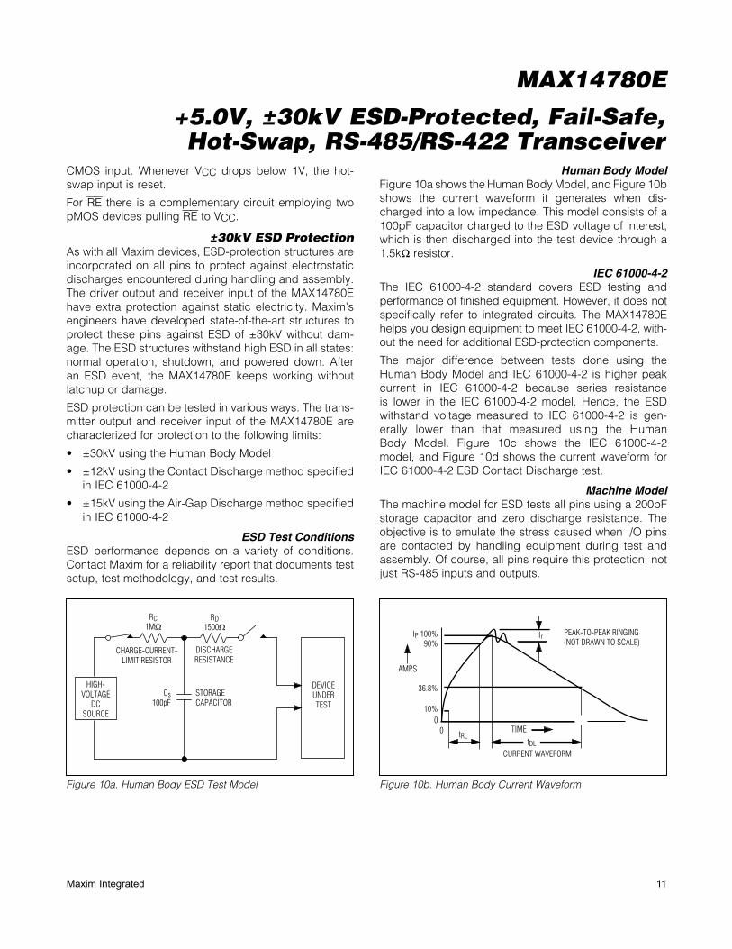
±30kV ESD ProtectionAs with all Maxim devices, ESD-protection structures are incorporated on all pins to protect against electrostatic discharges encountered during handling and assembly. The driver output and receiver input of the MAX14780E have extra protection against static electricity. Maxim’s engineers have developed state-of-the-art structures to protect these pins against ESD of ±30kV without dam-age. The ESD structures withstand high ESD in all states: normal operation, shutdown, and powered down. After an ESD event, the MAX14780E keeps working without latchup or damage.
ESD protection can be tested in various ways. The trans-mitter output and receiver input of the MAX14780E are characterized for protection to the following limits:
• ±30kV using the Human Body Model
• ±12kV using the Contact Discharge method specified in IEC 61000-4-2
• ±15kV using the Air-Gap Discharge method specified in IEC 61000-4-2
ESD Test ConditionsESD performance depends on a variety of conditions. Contact Maxim for a reliability report that documents test setup, test methodology, and test results.
Human Body ModelFigure 10a shows the Human Body Model, and Figure 10b shows the current waveform it generates when dis-charged into a low impedance. This model consists of a 100pF capacitor charged to the ESD voltage of interest, which is then discharged into the test device through a 1.5kΩ resistor.
IEC 61000-4-2The IEC 61000-4-2 standard covers ESD testing and performance of finished equipment. However, it does not specifically refer to integrated circuits. The MAX14780E helps you design equipment to meet IEC 61000-4-2, with-out the need for additional ESD-protection components.
The major difference between tests done using the Human Body Model and IEC 61000-4-2 is higher peak current in IEC 61000-4-2 because series resistance is lower in the IEC 61000-4-2 model. Hence, the ESD withstand voltage measured to IEC 61000-4-2 is gen-erally lower than that measured using the Human Body Model. Figure 10c shows the IEC 61000-4-2 model, and Figure 10d shows the current waveform for IEC 61000-4-2 ESD Contact Discharge test.
Machine ModelThe machine model for ESD tests all pins using a 200pF storage capacitor and zero discharge resistance. The objective is to emulate the stress caused when I/O pins are contacted by handling equipment during test and assembly. Of course, all pins require this protection, not just RS-485 inputs and outputs.
Figure 10a. Human Body ESD Test Model Figure 10b. Human Body Current Waveform
Applications InformationThe standard RS-485 receiver input impedance is 12kΩ (1-unit load), and the standard driver can drive up to 32-unit loads. The MAX14780E has a 1/8-unit load receiver input impedance (96kΩ), allowing up to 256 transceivers to be connected in parallel on one commu-nication line. Any combination of the MAX14780E, as well as other RS-485 transceivers with a total of 32-unit loads or fewer, can be connected to the line.
Reduced EMI and ReflectionsThe MAX14780E features reduced slew-rate drivers that minimize EMI and reduce reflections caused by improp-erly terminated cables, allowing error-free data transmis-sion up to 500kbps.
Low-Power Shutdown ModeLow-power shutdown mode is initiated by bringing both RE high and DE low. In shutdown, the devices typically draw only 2.8μA of supply current.
RE and DE can be driven simultaneously; the devices are guaranteed not to enter shutdown if RE is high and DE is low for less than 50ns. If the inputs are in this state for at least 700ns, the devices are guaranteed to enter shutdown.
Enable times tZH and tZL (see the Switching Characteristics section) assume the devices were not in a low-power shutdown state. Enable times tZH(SHDN) and tZL(SHDN) assume the devices were in shutdown state. It takes drivers and receivers longer to become enabled from low-power shutdown mode (tZH(SHDN), tZL(SHDN)) than from driver/receiver-disable mode (tZH, tZL).
Driver Output ProtectionTwo mechanisms prevent excessive output current and power dissipation caused by faults or by bus conten-tion. The first, a foldback current limit on the output stage, provides immediate protection against short cir-cuits over the whole common-mode voltage range (see the Typical Operating Characteristics). The second, a thermal-shutdown circuit, forces the driver outputs into a high-impedance state if the die temperature exceeds +175°C (typ).
Line LengthThe RS-485/RS-422 standard covers line lengths up to 4000ft. For line lengths greater than 4000ft, it may be necessary to implement a line repeater.
Figure 10c. IEC 61000-4-2 ESD Test Model Figure 10d. IEC 61000-4-2 ESD Generator Current Waveform
Typical ApplicationsThe MAX14780E transceiver is designed for bidirectional data communications on multipoint bus transmission lines. Figure 11 shows a typical network applications circuit.
To minimize reflections, terminate the line at both ends in its characteristic impedance, and keep stub lengths off the main line as short as possible. The slew-rate-limited MAX14780E is more tolerant of imperfect termination.
Chip InformationPROCESS: BiCMOS
Package InformationFor the latest package outline information and land patterns (foot-prints), go to www.maximintegrated.com/packages. Note that a “+”, “#”, or “-” in the package code indicates RoHS status only. Package drawings may show a different suffix character, but the drawing pertains to the package regardless of RoHS status.
Maxim Integrated cannot assume responsibility for use of any circuitry other than circuitry entirely embodied in a Maxim Integrated product. No circuit patent licenses are implied. Maxim Integrated reserves the right to change the circuitry and specifications without notice at any time. The parametric values (min and max limits) shown in the Electrical Characteristics table are guaranteed. Other parametric values quoted in this data sheet are provided for guidance.
1 7/11 Added PDIP package information to data sheet 1, 2 , 9, 13
2 10/11Updated DC Electrical Characteristics including adding new row for Input Impedance on First Transition after POR Delay, updated Hot-Swap Input Circuitry section
2, 10
3 1/15 Updated General Description and Benefits and Features sections 1