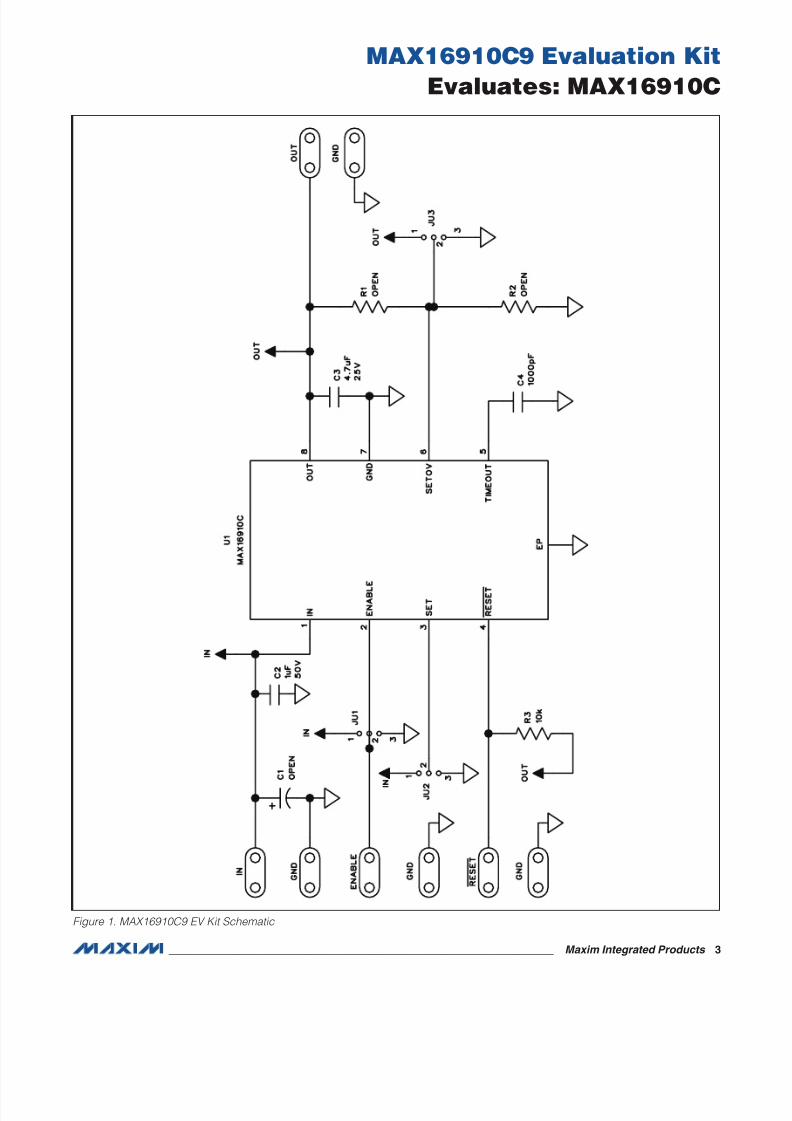
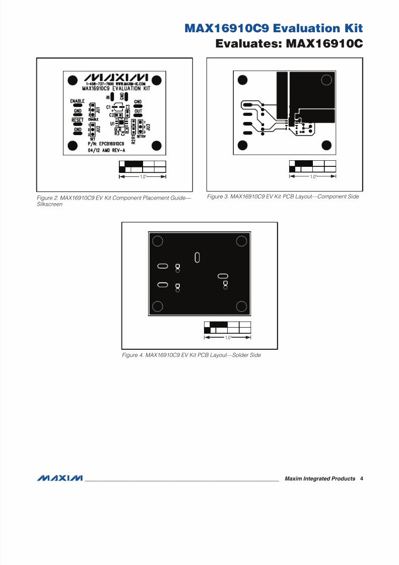
Date post: | 14-Apr-2018 |
Category: |
Documents |
Upload: | samdaniel08 |
View: | 213 times |
Download: | 0 times |
7/27/2019 MAX16910C9EVKIT
http://slidepdf.com/reader/full/max16910c9evkit 1/6
General Description
The MAX16910C9 evaluation kit (EV kit) is a fully assem-bled and tested PCB for evaluating the MAX16910C low-
dropout (LDO) linear regulator. The EV kit circuit can be
configured as either a fixed output voltage (3.3V or 5V)
or an adjustable output voltage. The EV kit provides up
200mA current at the circuit output. The EV kit operates
from a 3.5V to 30V supply.
The EV kit comes with the MAX16910CASA9 92.5%
output-voltage reset-threshold IC installed. The EV kit
can also evaluate the MAX16910CASA8 IC, which has an
87% output voltage reset threshold.
Features
S 3.5V to 30V Input Voltage Range
S Configurable for 3.3V or 5V Output Voltage
S Resistor PCB Pads for Adjusting the Output
Voltage (1.5V to 11V)
S Provides Up to 200mA Output Current
S Low-Dropout Voltage of 280mV at 200mA
S RESET Power-Good Output
S Proven PCB Layout
S Fully Assembled and Tested
Component Supplier
DESIGNATION QTY DESCRIPTION
C1 0Not installed, electrolytic
capacitor
C2 1
1FF Q10%, 50V X7R ceramic
capacitor (0805)
TDK C2012X7R1H105K
C3 1
4.7FF Q10%, 25V X7R ceramic
capacitor (0805)
TDK C2012X7R1E475K
C4 1
1000pF 10%, 50V X7R ceramic
capacitor (0603)
TDK C1608X7R1H102k
DESIGNATION QTY DESCRIPTION
JU1, JU2, JU3 3 3-pin headers
R1, R2 0 Not installed, resistors (0805)
R3 1 10kI Q5% resistor (0603)
U1 1
200mA automotive linear
regulator (8 SO-EP*)
Maxim MAX16910CASA9/V+
— 3 Shunts
— 1PCB: MAX16910C9
EVALUATION KIT
SUPPLIER PHONE WEBSITE
TDK Corp. 847-699-2299 www.component.tdk.com
MAX16910C9 Evaluation Kit
Evaluates: MAX16910C
_________________________________________________________________ Maxim Integrated Products 1
For pricing, delivery, and ordering information, please contact Maxim Direct at 1-888-629-4642,
or visit Maxim’s website at www.maxim-ic.com.
Component List
19-6287; Rev 0; 4/12
Ordering Information appears at end of data sheet.
*EP = Exposed pad.
Note: Indicate that you are using the MAX16910C9 when
contacting this component supplier.
7/27/2019 MAX16910C9EVKIT
http://slidepdf.com/reader/full/max16910c9evkit 2/6
SHUNT
POSITIONENABLE PIN OUTPUT
1- 2 Connected to IN Enabled
2-3 Connected to GND Disabled
SHUNT POSITIONOUTPUT VOLTAGE
JU2 JU3
1 -2 Not installedSet by external feedback
resistors R1 and R2
2 -31-2 5V
2-3 3.3V
_________________________________________________________________ Maxim Integrated Products 2
MAX16910C9 Evaluation Kit
Evaluates: MAX16910C
Quick Start
Required Equipment • MAX16910C9EVkit
• 3.5Vto30V,300mApowersupply
• Electronicloadcapableofsinking200mA
• Digitalmultimeter(DMM)
Procedure The EV kit is fully assembled and tested. Follow the steps
below to verify board operation:
1) Verify that shunts are installed across jumpers JU1
(1-2), JU2 (2-3), and JU3 (1-2).
2) Set the power supply to 14V and disable the output.
3) Connect the positive input of the DMM to the OUT
PCB pad on the EV kit, and the negative input of the
DMM to the GND PCB pad on the EV kit to measurethe output voltage.
4) Connect the 200mA load between the OUT and GND
PCB pads on the EV kit.
5) Enable the power-supply output.
6) Verify that the output voltage is 5V.
Detailed Description of Hardware
The MAX16910C9 EV kit is a fully assembled and tested
PCB for evaluating the MAX16910CASA9 200mA LDO
regulator. The EV kit operates from 3.5V to 30V and
requires 300mA current.
The LDO regulator has a fixed 3.3V or 5V output, but can
be configured between 1.5V and 11V. An open-drain
RESET output changes from low to high whenever the
OUT voltage rises to 92.5% of its regulated output. When
OUT exceeds its rising threshold voltage, RESET remains
low for the 1.25ms reset timeout period programmed by
capacitor C4, and then goes high. A RESET PCB pad is
available for monitoring the output.
Enable (JU1) Jumper JU1 configures the EV kit’s output for turn-on/
off control. Install a shunt across pins 1-2 to enable the
circuit output. Install a shunt across pins 2-3 to disable
the output. The output can also be externally controlledby placing an independent voltage source at the ENABLE
PCB pad when a shunt is not installed at JU1. See Table 1
for proper JU1 configuration.
Output-Voltage Selection
Jumpers JU2 and JU3 configure the EV kit circuit to oper-
ate in fixed output-voltage or adjustable output-voltage
mode.
In fixed output-voltage mode, the output voltage is set
to 3.3V or 5V using jumper JU3. To configure the EV kit
circuit for fixed output mode, install a shunt across pins
2-3 on jumper JU2. Place a shunt across pins 1-2 on JU3
for the 5V preset output. Place a shunt across pins 2-3 for
the 3.3V preset output.
In adjustable output-voltage mode, the output voltage
is set using a resistor-divider network from the OUT
to SETOV pins. To configure the circuit for adjustable
output-voltage mode, install a shunt across pins 1-2 on
jumper JU2 and remove the shunt at jumper JU3. The
output voltage can be set between 1.5V to 11V using
surface-mount 0805 resistor PCB pads R1 and R2.
To set the output voltage, select resistor R2 to be less
than or equal to 100kI and use the following equation
to compute R1:
( )OUT
SETOV
V
R1 R2 1V= × −
where VOUT is the desired output voltage, VSETOV is
1.25V, and R1 is in kI.
See Table 2 for proper jumper configurations when
operating the EV kit circuit in fixed or adjustable output-
voltage mode.
RESET Output The IC has an open-drain RESET output that goes high
impedance after the output rises 92.5% (typ) above its
regulated output. Pullup resistor R3 pulls the RESET PCB
pad up to the OUT voltage.
Table 1. Enable Control (JU1)
Table 2. Output-Voltage Configurations(JU2, JU3)
7/27/2019 MAX16910C9EVKIT
http://slidepdf.com/reader/full/max16910c9evkit 3/6
_________________________________________________________________ Maxim Integrated Products 3
MAX16910C9 Evaluation Kit
Evaluates: MAX16910C
Figure 1. MAX16910C9 EV Kit Schematic
7/27/2019 MAX16910C9EVKIT
http://slidepdf.com/reader/full/max16910c9evkit 4/6
1.0’’
1.0’’1.0’’
_________________________________________________________________ Maxim Integrated Products 4
MAX16910C9 Evaluation Kit
Evaluates: MAX16910C
Figure 2. MAX16910C9 EV Kit Component Placement Guide— Silkscreen
Figure 3. MAX16910C9 EV Kit PCB Layout—Component Side
Figure 4. MAX16910C9 EV Kit PCB Layout—Solder Side
7/27/2019 MAX16910C9EVKIT
http://slidepdf.com/reader/full/max16910c9evkit 5/6
PART EV Kit
MAX16910C9EVKIT# EV Kit
_________________________________________________________________ Maxim Integrated Products 5
MAX16910C9 Evaluation Kit
Evaluates: MAX16910C
Ordering Information
#Denotes RoHS compliant.
7/27/2019 MAX16910C9EVKIT
http://slidepdf.com/reader/full/max16910c9evkit 6/6
REVISION
NUMBER
REVISION
DATEDESCRIPTION
PAGES
CHANGED
0 4/12 Initial release —
Maxim cannot assume responsibility for use of any circuitry other than circuitry entirely embodied in a Maxim product. No circuit patent licenses are implied.
Maxim reserves the right to change the circuitry and specifications without notice at any time.
Maxim Integrated Products, 120 San Gabriel Drive, Sunnyvale, CA 94086 408-737-7600 6
©2012 Maxim Integrated Products Maxim is a registered trademark of Maxim Integrated Products, Inc.
MAX16910C9 Evaluation Kit
Evaluates: MAX16910C
Revision History