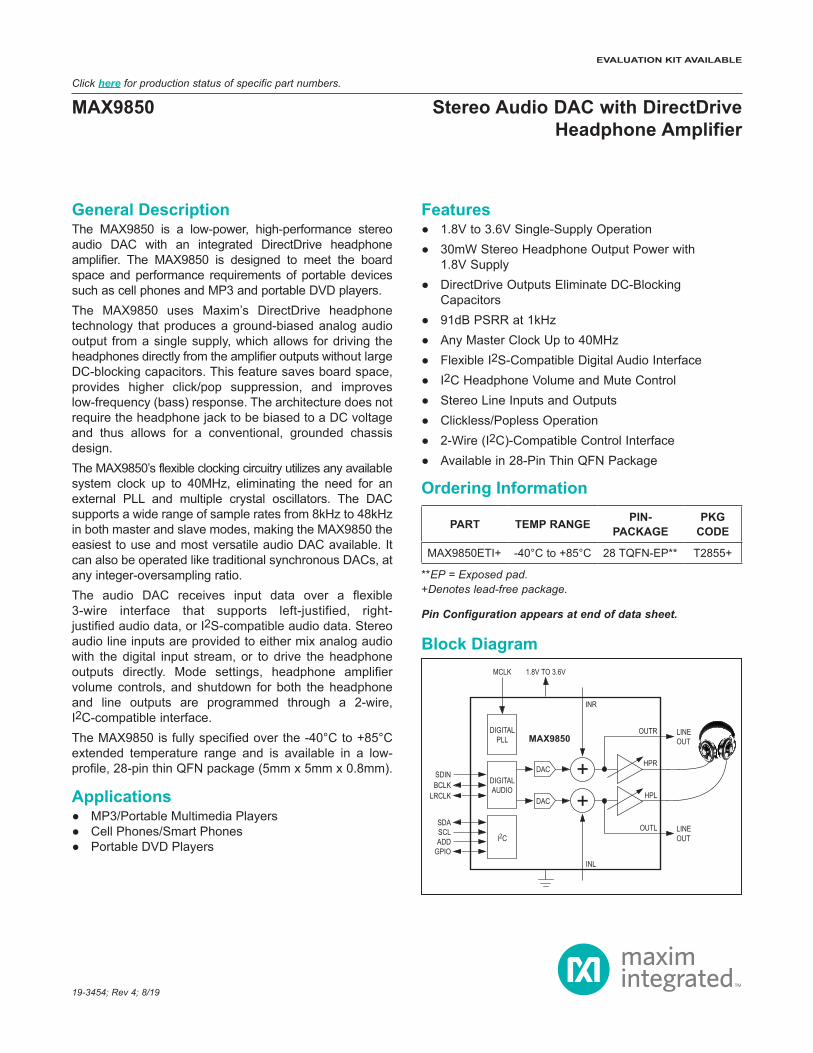
General Description The MAX9850 is a low-power, high-performance stereo audio DAC with an integrated DirectDrive headphone amplifier. The MAX9850 is designed to meet the board space and performance requirements of portable devices such as cell phones and MP3 and portable DVD players. The MAX9850 uses Maxim’s DirectDrive headphone technology that produces a ground-biased analog audio output from a single supply, which allows for driving the headphones directly from the amplifier outputs without large DC-blocking capacitors. This feature saves board space, provides higher click/pop suppression, and improves low-frequency (bass) response. The architecture does not require the headphone jack to be biased to a DC voltage and thus allows for a conventional, grounded chassis design. The MAX9850’s flexible clocking circuitry utilizes any available system clock up to 40MHz, eliminating the need for an external PLL and multiple crystal oscillators. The DAC supports a wide range of sample rates from 8kHz to 48kHz in both master and slave modes, making the MAX9850 the easiest to use and most versatile audio DAC available. It can also be operated like traditional synchronous DACs, at any integer-oversampling ratio. The audio DAC receives input data over a flexible 3-wire interface that supports left-justified, right- justified audio data, or I 2 S-compatible audio data. Stereo audio line inputs are provided to either mix analog audio with the digital input stream, or to drive the headphone outputs directly. Mode settings, headphone amplifier volume controls, and shutdown for both the headphone and line outputs are programmed through a 2-wire, I 2 C-compatible interface. The MAX9850 is fully specified over the -40°C to +85°C extended temperature range and is available in a low- profile, 28-pin thin QFN package (5mm x 5mm x 0.8mm). Applications ● MP3/Portable Multimedia Players ● Cell Phones/Smart Phones ● Portable DVD Players Features ● 1.8V to 3.6V Single-Supply Operation ● 30mW Stereo Headphone Output Power with 1.8V Supply ● DirectDrive Outputs Eliminate DC-Blocking Capacitors ● 91dB PSRR at 1kHz ● Any Master Clock Up to 40MHz ● Flexible I 2 S-Compatible Digital Audio Interface ● I 2 C Headphone Volume and Mute Control ● Stereo Line Inputs and Outputs ● Clickless/Popless Operation ● 2-Wire (I 2 C)-Compatible Control Interface ● Available in 28-Pin Thin QFN Package 19-3454; Rev 4; 8/19 Pin Configuration appears at end of data sheet. **EP = Exposed pad. +Denotes lead-free package. PART TEMP RANGE PIN- PACKAGE PKG CODE MAX9850ETI+ -40°C to +85°C 28 TQFN-EP** T2855+ Ordering Information Block Diagram DAC DAC DIGITAL AUDIO DIGITAL PLL I 2 C MAX9850 SDIN BCLK LRCLK SDA SCL ADD GPIO LINE OUT LINE OUT OUTR HPR HPL OUTL INL INR 1.8V TO 3.6V MCLK MAX9850 Stereo Audio DAC with DirectDrive Headphone Amplifier EVALUATION KIT AVAILABLE Click here for production status of specific part numbers.
Transcript
General DescriptionThe MAX9850 is a low-power, high-performance stereo audio DAC with an integrated DirectDrive headphone amplifier. The MAX9850 is designed to meet the board space and performance requirements of portable devices such as cell phones and MP3 and portable DVD players.The MAX9850 uses Maxim’s DirectDrive headphone technology that produces a ground-biased analog audio output from a single supply, which allows for driving the headphones directly from the amplifier outputs without large DC-blocking capacitors. This feature saves board space, provides higher click/pop suppression, and improves low-frequency (bass) response. The architecture does not require the headphone jack to be biased to a DC voltage and thus allows for a conventional, grounded chassis design.The MAX9850’s flexible clocking circuitry utilizes any available system clock up to 40MHz, eliminating the need for an external PLL and multiple crystal oscillators. The DAC supports a wide range of sample rates from 8kHz to 48kHz in both master and slave modes, making the MAX9850 the easiest to use and most versatile audio DAC available. It can also be operated like traditional synchronous DACs, at any integer-oversampling ratio.The audio DAC receives input data over a flexible 3-wire interface that supports left-justified, right- justified audio data, or I2S-compatible audio data. Stereo audio line inputs are provided to either mix analog audio with the digital input stream, or to drive the headphone outputs directly. Mode settings, headphone amplifier volume controls, and shutdown for both the headphone and line outputs are programmed through a 2-wire, I2C-compatible interface.The MAX9850 is fully specified over the -40°C to +85°C extended temperature range and is available in a low- profile, 28-pin thin QFN package (5mm x 5mm x 0.8mm).
Applications MP3/Portable Multimedia Players Cell Phones/Smart Phones Portable DVD Players
Features 1.8V to 3.6V Single-Supply Operation 30mW Stereo Headphone Output Power with
Capacitors 91dB PSRR at 1kHz Any Master Clock Up to 40MHz Flexible I2S-Compatible Digital Audio Interface I2C Headphone Volume and Mute Control Stereo Line Inputs and Outputs Clickless/Popless Operation 2-Wire (I2C)-Compatible Control Interface Available in 28-Pin Thin QFN Package
19-3454; Rev 4; 8/19
Pin Configuration appears at end of data sheet.
**EP = Exposed pad.+Denotes lead-free package.
PART TEMP RANGE PIN-PACKAGE
PKG CODE
MAX9850ETI+ -40°C to +85°C 28 TQFN-EP** T2855+
Ordering Information
Block Diagram
DAC
DAC
DIGITALAUDIO
DIGITALPLL
I2C
MAX9850
SDINBCLK
LRCLK
SDASCLADD
GPIO
LINEOUT
LINEOUT
OUTR
HPR
HPL
OUTL
INL
INR
1.8V TO 3.6VMCLK
MAX9850 Stereo Audio DAC with DirectDrive Headphone Amplifier
EVALUATION KIT AVAILABLE
Click here for production status of specific part numbers.
(Voltages with respect to AGND.)DVDD, AVDD, PVDD ................................................-0.3V to +4VAVDD Referenced to PVDD ..................................-0.3V to +0.3VSVSS, PVSS ............................................................-4V to +0.3VSVSS Referenced to PVSS ...................................-0.3V to +0.3VDGND, PGND ......................................................-0.3V to +0.3VBCLK, LRCLK, HPS, SDIN ....................-0.3V to (DVDD + 0.3V)GPIO, MCLK ...........................................................-0.3V to +4VREF, PREG ............................................ -0.3V to (AVDD + 0.3V)NREG ..................................................... +0.3V to (SVSS - 0.3V)SDA, SCL, ADD.......................................................-0.3V to +4VINL, INR ......................................................................-2V to +2VHPR, HPL ................................. (SVSS - 0.3V) to (AVDD + 0.3V)
OUTL, OUTR .......................... (NREG - 0.3V) to (PREG + 0.3V)C1N ......................................... (PVSS - 0.3V) to (PGND + 0.3V)C1P .......................................... (PGND - 0.3V) to (PVDD + 0.3V)Current Into/Out of Any Pin ..............................................100mADuration of HPL, HPR, OUTL,
OUTR Short Circuit to AGND ................................ContinuousContinuous Power Dissipation (TA = +70°C)
28-Pin Thin QFN (derate 35.7mW/°C above +70°C) ...2857mWJunction Temperature ......................................................+150°COperating Temperature Range ........................... -40°C to +85°CStorage Temperature Range ............................ -65°C to +150°CLead Temperature (soldering, 10s) .................................+300°C
(DVDD = AVDD = PVDD=3.0V,AGND=DGND=PGND=0V,C1=0.47μF,C2=2.2μF,CNREG = CPREG = CREF=1μFtoAGND,RLOAD_HP=32ΩtoAGND,RLOAD_OUT=10kΩtoAGND,fLRCLK = 48kHz, fMCLK = 12.288MHz, volume set to -9.5dB, TA = TMIN to TMAX, unless otherwise noted. Typical specifications at TA = +25°C, unless otherwise noted.) (Note 1)
PARAMETER SYMBOL CONDITIONS MIN TYP MAX UNITS
Analog Supply Voltage AVDD, PVDD
AVDD = PVDD 1.8 3.6 V
Digital Supply Voltage DVDD 1.8 3.6 V
Analog Supply Current AIDD
Full operation (Note 2), no headphone or line output load
AVDD = 1.8V 5.5 7.7
mAAVDD = 3.0V 5.9
Full operation (Note 2), headphones disabled
AVDD = 1.8V 3.5 5.3
AVDD = 3.0V 3.75
Digital Supply Current DIDDFull operation (Note 2), no line output load
DVDD = 1.8V 2.1 2.9mA
DVDD = 3.0V 3.8
Analog Shutdown Current AISHDN IAVDD + IPVDD, AVDD = PVDD = 1.8V 1.5 10 µA
Digital Shutdown Current DISHDN Static digital interface, DVDD = 1.8V 0.3 5 µA
Shutdown to Full Operation(Note 2) tON 1.3 ms
Power-On to Full Operation(Note 2) tPON 1.4 ms
DAC PERFORMANCE/LINE OUTPUTS (Note 3)
0dBFS Output Voltage VOUT_FS 1.85 1.95 2.05 VP-P
Dynamic Range (Note 4) DRAVDD = 3.0V 87.5
dBAVDD = 1.8V 82 87.5
Signal-to-Noise Ratio(Note 5) SNR
Unweighted 88
dBA-weighted 91
AVDD = 1.8V, unweighted 88
AVDD = 1.8V, A-weighted 91
Absolute Maximum Ratings
Stresses beyond those listed under “Absolute Maximum Ratings” may cause permanent damage to the device. These are stress ratings only, and functional operation of the device at these or any other conditions beyond those indicated in the operational sections of the specifications is not implied. Exposure to absolute maximum rating conditions for extended periods may affect device reliability.
Electrical Characteristics
MAX9850 Stereo Audio DAC with DirectDrive Headphone Amplifier
www.maximintegrated.com Maxim Integrated 2
(DVDD = AVDD = PVDD=3.0V,AGND=DGND=PGND=0V,C1=0.47μF,C2=2.2μF,CNREG = CPREG = CREF=1μFtoAGND,RLOAD_HP=32ΩtoAGND,RLOAD_OUT=10kΩtoAGND,fLRCLK = 48kHz, fMCLK = 12.288MHz, volume set to -9.5dB, TA = TMIN to TMAX, unless otherwise noted. Typical specifications at TA = +25°C, unless otherwise noted.) (Note 1)
PARAMETER SYMBOL CONDITIONS MIN TYP MAX UNITS
Total Harmonic Distortion Plus Noise THD+N fIN = 984.375Hz
0dBFS 87
dB
-60dBFS 27.5
AVDD = 1.8V, 0dBFS -81
AVDD = 1.8V,-60dBFS -27.5 -22
Line Output Offset Voltage VOS_LINE -15 0 +15 mV
Channel-to-Channel Gain Matching ΔAV/AV OUTL to OUTR, OUTR to OUTL ±0.04 dB
Power-Supply Rejection Ratio PSRR
VRIPPLE = 100mVP-P, fIN = 1kHz, applied to AVDD and PVDD
87dB
VRIPPLE = 100mVP-P, fIN = 20kHz, applied to AVDD and PVDD
67
Crosstalk XTALK fOUT = 1kHz, VOUT = 2VP-P(OUTL to OUTR) or (OUTR to OUTL) -105 dB
Sampling Frequency Range fS 8 48 kHz
MCLK Frequency fMCLK 8.448 40 MHz
DAC 8x INTERPOLATION FILTER
Passband Frequency PB To -1dB corner 0 0.48 x fS kHz
Frequency Response FR 10Hz to 20kHz -0.1 +0.1 dB
Stopband Attenuation SBA 58 dB
Stopband Frequency SB Attenuation greater than SBA 0.58 x fS 7.42 x fS kHz
LINE INPUTS (INL, INR)
Line Input Voltage VIN_LINE -1 +1 V
IN_ to OUT_ Gain AV_LINE -1.05 -1 -0.95 V/V
Line Input Bias Voltage VBIAS_LINE -15 0 +15 mV
INL and INR Input Resistance RIN_LINE 10 22 kΩ
INTERNAL REGULATORS (NREG, PREG)
PREG Output Voltage VPREG 1.60 V
NREG Output Voltage VNREG -1.15 V
REF Output Voltage VREF 1.23 V
Electrical Characteristics (continued)
MAX9850 Stereo Audio DAC with DirectDrive Headphone Amplifier
www.maximintegrated.com Maxim Integrated 3
(DVDD = AVDD = PVDD=3.0V,AGND=DGND=PGND=0V,C1=0.47μF,C2=2.2μF,CNREG = CPREG = CREF=1μFtoAGND,RLOAD_HP=32ΩtoAGND,RLOAD_OUT=10kΩtoAGND,fLRCLK = 48kHz, fMCLK = 12.288MHz, volume set to -9.5dB, TA = TMIN to TMAX, unless otherwise noted. Typical specifications at TA = +25°C, unless otherwise noted.) (Note 1)
PARAMETER SYMBOL CONDITIONS MIN TYP MAX UNITS
HEADPHONE OUTPUTS (HPL, HPR)
Output Power OUTTHD+N = 1%fIN = 1kHz, headphonevolume = +6dB
RL =16ΩAVDD = 3.0V 95
mW
RL =32ΩAVDD = 3.0V 40 65
RL =16ΩAVDD = 1.8V 30
RL =32ΩAVDD = 1.8V 15 25
Full-Scale Headphone Amplifier Output Voltage VOUT_FS Volume = +5dB, HP unloaded 1.16 1.23 1.30 VRMS
Line In to HP Output Voltage Gain AV_HP Volume = +3dB, HP unloaded 1.34 1.41 1.48 V/V
Total Harmonic Distortion Plus Noise THD+N
RL =32Ω,POUT = 60mW, fIN = 1kHz -94dB
RL =16Ω,POUT = 60mW, fIN = 1kHz -90
Signal-to-Noise Ratio (Note 6) SNR
Unweighted 88
dBA-weighted 90
AVDD = 1.8V, unweighted 88
AVDD = 1.8V, A-weighted 91
Power-Supply Rejection Ratio PSRR
VRIPPLE = 100mVP-P, frequency = 1kHz, applied to AVDD and PVDD
91dB
VRIPPLE = 100mVP-P, frequency = 20kHz, applied to AVDD and PVDD
72
Headphone Output Offset Voltage VOS_HP Volume = -11.5dB
TA = +25°C -15 +15mV
TA = TMIN to TMAX -25 +25
Slew Rate SR 0.47 V/µs
Maximum Capacitive Load CL No sustained oscillations 150 pF
Crosstalk XTALK RHP=32Ω,POUT = 3.5mW, fIN = 1kHz (HPL to HPR) or (HPR to HPL) -85 dB
Channel-to-Channel Gain Matching ΔAV/AV ±0.05 dB
Internal Charge-Pump Oscillator Frequency fCP 550 667 775 kHz
Charge-Pump Operating Frequency Range Charge-pump clock derived from MCLK 550 775 kHz
Volume Control Range -73.5 +6.0 dB
Electrical Characteristics (continued)
MAX9850 Stereo Audio DAC with DirectDrive Headphone Amplifier
www.maximintegrated.com Maxim Integrated 4
(DVDD = AVDD = PVDD=3.0V,AGND=DGND=PGND=0V,C1=0.47μF,C2=2.2μF,CNREG = CPREG = CREF=1μFtoAGND,RLOAD_HP=32ΩtoAGND,RLOAD_OUT=10kΩtoAGND,fLRCLK = 48kHz, fMCLK = 12.288MHz, volume set to -9.5dB, TA = TMIN to TMAX, unless otherwise noted. Typical specifications at TA = +25°C, unless otherwise noted.) (Note 1)
PARAMETER SYMBOL CONDITIONS MIN TYP MAX UNITS
Mute Attenuation 100 dB
DIGITAL INPUTS (GPIO, SCL, SDA, BCLK, LRCLK, SDIN, ADD, MCLK)
Input High Voltage VIH0.8 x DVDD
V
Input Low Voltage VIL0.2 x DVDD
V
Input Leakage Current IIH, IIL VIH = DVDD, VIL = DGND -10 +10 µA
Input-High Leakage Current IIHFull shutdown, VIH = DVDD 400
µANormal operation, VIH = DVDD 1
Input-Low Leakage Current IILFull shutdown, VIL = DGND 1
µANormal operation, VIL = DGND 100
Input Hysteresis 0.05 x DVDD
V
Electrical Characteristics (continued)
MAX9850 Stereo Audio DAC with DirectDrive Headphone Amplifier
www.maximintegrated.com Maxim Integrated 5
(DVDD = AVDD = PVDD=3.0V,AGND=DGND=PGND=0V,C1=0.47μF,C2=2.2μF,CNREG = CPREG = CREF=1μFtoAGND,RLOAD_HP=32ΩtoAGND,RLOAD_OUT=10kΩtoAGND,fLRCLK = 48kHz, fMCLK = 12.288MHz, volume set to -9.5dB, TA = TMIN to TMAX, unless otherwise noted. Typical specifications at TA = +25°C, unless otherwise noted.) (Note 1)
Note 1: The MAX9850 is 100% production tested at TA = +25°C and is guaranteed by design for TA = TMIN to TMAX.Note 2: Full operation is defined as clocking all zeros into the DAC while the DAC, headphone outputs, and line outputs are all
enabled.Note 3: DAC performance specifications measured using the line outputs, OUTL and OUTR.Note 4: Dynamic range is defined as the SNR of a 1kHz, -60dBFS input signal measured with an A-weighted filter, then normalized
to full scale (+60dB).
PARAMETER SYMBOL CONDITIONS MIN TYP MAX UNITS
I2C TIMING
Serial Clock Frequency fSCL 0 400 kHz
Bus Free Time Between STOP and START Conditions tBUF 1.3 µs
Hold Time (Repeated) START Condition tHD, STA 0.6 µs
SCL Pulse-Width Low tLOW 1.3 µs
SCL Pulse-Width High tHIGH 0.6 µs
Repeated START Condition Setup Time tSU, STA 0.6 µs
Data Hold Time tHD, DAT 0 900 ns
Data Setup Time tSU, DAT 100 ns
Bus Capacitance CB 400 pF
SDA and SCL Receiving Rise Time (Note 8) tR 20 + 0.1CB 300 ns
SDA and SCL Receiving Fall Time (Note 8) tF 20 + 0.1CB 300 ns
SDA Transmitting Fall Time (Note 8) tF
DVDD = 1.8V, TA = +25°C 20 + 0.1CB 250ns
DVDD = 3.6V, TA = +25°C 20 + 0.5CB 250
Setup Time for STOP Condition tSU, STO 0.6 µs
Pulse Width of Suppressed Spike tSP 0 50 ns
DIGITAL AUDIO TIMING
BCLK Period (Note 9) tBCLK 3 x 1/fICLK ns
Low or High BCLK Pulse Width tBCLK_PW 0.35 x tBCLK ns
BCLK and LRCLK Rise Time tR Master mode, CLOAD = 15pF 1 ns
BCLK and LRCLK Fall Time tF Master mode, CLOAD = 15pF 1 ns
SDIN or LRCLK to BCLK Rising Setup Time
tDBSU, tBWSU
30 ns
SDIN or LRCLK to BCLK Rising Hold Time
tDBH, tBWBH
DVDD = 1.8V 0ns
DVDD = 3.6V 5
Electrical Characteristics (continued)
MAX9850 Stereo Audio DAC with DirectDrive Headphone Amplifier
www.maximintegrated.com Maxim Integrated 6
Note 5: DAC SNR measured from DAC inputs to OUTL and OUTR.Note 6: Headphone amplifier SNR measured from line inputs to headphone outputs.Note 7: GPIOis100kΩtogroundwhenDVDD < VOH < 3.6V.Note 8: CB is in pF.Note 9: fICLK derived by dividing fMCLK by 1, 2, 3, or 4. See the Registers and Bit Descriptions section.
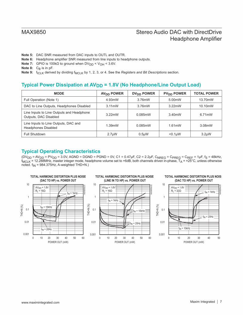
(DVDD = AVDD = PVDD=3.0V,AGND=DGND=PGND=0V,C1=0.47μF,C2=2.2μF,CNREG = CPREG = CREF=1μF,fS = 48kHz, fMCLK = 12.288MHz, master integer mode, headphone volume set to +6dB, both channels driven in-phase, TA = +25°C, unless otherwise noted. fIN = 984.375Hz, A-weighted THD+N.)
MODE AVDD POWER DVDD POWER PVDD POWER TOTAL POWER
Full Operation (Note 1) 4.93mW 3.76mW 5.00mW 13.70mW
DAC to Line Outputs, Headphones Disabled 3.11mW 3.76mW 3.22mW 10.10mW
Line Inputs to Line Outputs and Headphone Outputs, DAC Disabled 3.22mW 0.085mW 3.40mW 6.71mW
Line Inputs to Line Outputs, DAC and Headphones Disabled 1.39mW 0.085mW 1.61mW 3.08mW
Full Shutdown 2.7µW 0.5µW <0.1µW 3.2µW
Typical Power Dissipation at AVDD = 1.8V (No Headphone/Line Output Load)
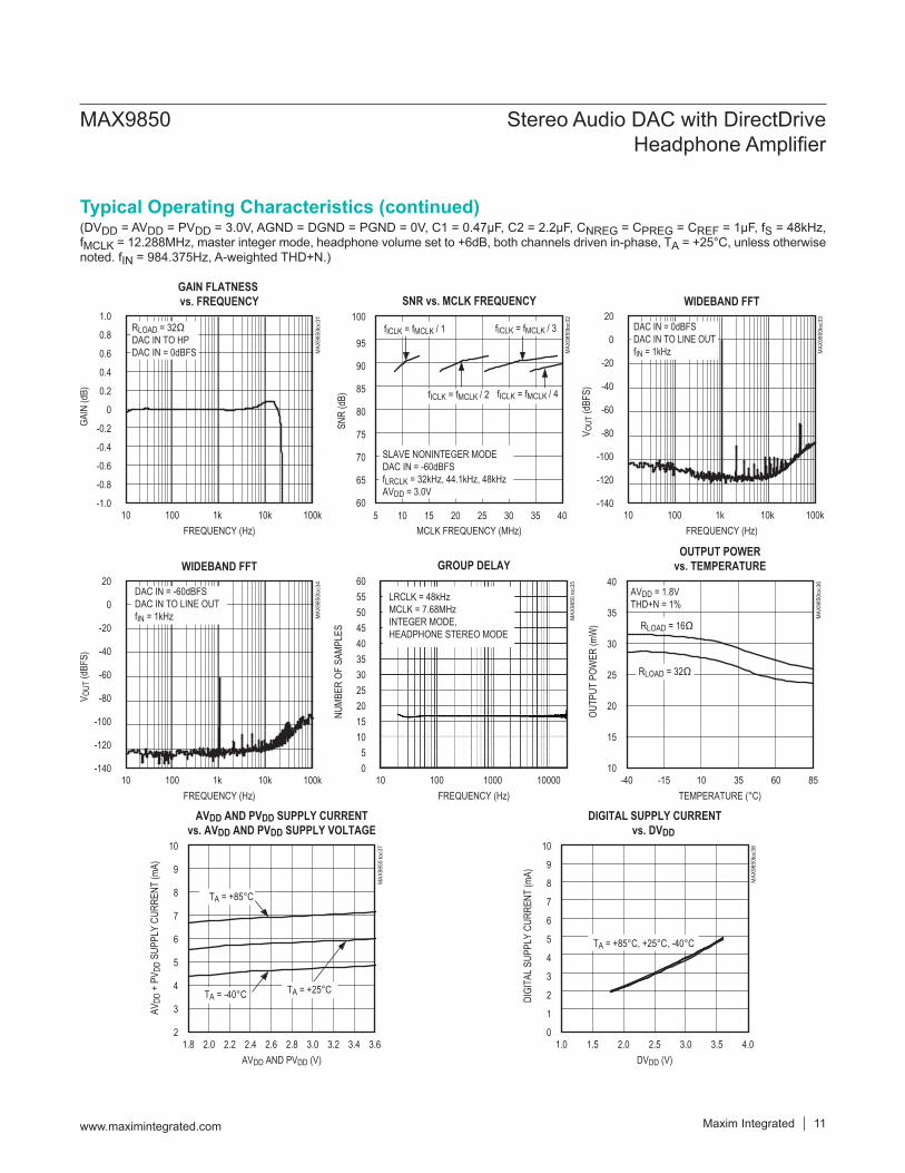
Typical Operating Characteristics
10
0.0010 2010 40 60
TOTAL HARMONIC DISTORTION PLUS NOISE (LINE IN TO HP) vs. POWER OUT
0.01
0.1
1
MAX
9850
toc0
2
POWER OUT (mW)
THD+
N (%
)
30 50
AVDD = 1.8VRL = 16Ω
fIN = 10kHz
fIN = 20Hz
fIN = 1kHz
10
0.0010 2010 40 50
TOTAL HARMONIC DISTORTION PLUS NOISE(DAC TO HP) vs. POWER OUT
0.01
0.1
1
MAX
9850
toc0
3
POWER OUT (mW)
THD+
N (%
)
30
AVDD = 1.8VRL = 32Ω fIN = 1kHz
fIN = 10kHz
fIN = 20Hz
10
0.0010 2010 40 60
TOTAL HARMONIC DISTORTION PLUS NOISE(DAC TO HP) vs. POWER OUT
0.01
0.1
1
MAX
9850
toc0
1
POWER OUT (mW)
THD+
N (%
)
30 50
AVDD = 1.8VRL = 16Ω
fIN = 1kHz
fIN = 10kHz
fIN = 20Hz
MAX9850 Stereo Audio DAC with DirectDrive Headphone Amplifier
www.maximintegrated.com Maxim Integrated 7
(DVDD = AVDD = PVDD=3.0V,AGND=DGND=PGND=0V,C1=0.47μF,C2=2.2μF,CNREG = CPREG = CREF=1μF,fS = 48kHz, fMCLK = 12.288MHz, master integer mode, headphone volume set to +6dB, both channels driven in-phase, TA = +25°C, unless otherwise noted. fIN = 984.375Hz, A-weighted THD+N.)
Typical Operating Characteristics (continued)
10
0.0010 4020 100
TOTAL HARMONIC DISTORTION PLUS NOISE(LINE IN TO HP) vs. POWER OUT
0.01
0.1
1
MAX
9850
toc0
6
POWER OUT (mW)
THD+
N (%
)
60 80
AVDD = 3.0VRL = 16Ω
fIN = 20Hz
fIN = 1kHz
fIN = 10kHz
10
0.00110 100 10k 100k
TOTAL HARMONIC DISTORTION PLUS NOISE(DAC TO HP) vs. FREQUENCY
0.01
0.1
1
MAX
9850
toc0
9
FREQUENCY (Hz)
THD+
N (%
)
1k
AVDD = 1.8VRL = 16Ω
POUT = 5mW
POUT = 21mW
10
0.00110 100 10k 100k
TOTAL HARMONIC DISTORTION PLUS NOISE(DAC TO HP) vs. FREQUENCY
0.01
0.1
1
MAX
9850
toc1
2
FREQUENCY (Hz)
THD+
N (%
)
1k
AVDD = 3.0VRL = 16Ω
POUT = 10mW
POUT = 60mW
10
0.0010 4020 100
TOTAL HARMONIC DISTORTION PLUS NOISE(DAC TO HP) vs. POWER OUT
0.01
0.1
1
MAX
9850
toc0
5
POWER OUT (mW)
THD+
N (%
)
60 80
AVDD = 3.0VRL = 16Ω
fIN = 1kHz
fIN = 10kHz
fIN = 20Hz
10
0.0010 4020 100
TOTAL HARMONIC DISTORTION PLUS NOISE(LINE IN TO HP) vs. POWER OUT
0.01
0.1
1
MAX
9850
toc0
8
POWER OUT (mW)
THD+
N (%
)
60 80
AVDD = 3.0VRL = 32Ω
fIN = 1kHz
fIN = 10kHzfIN = 20Hz
10
0.00110 100 10k 100k
TOTAL HARMONIC DISTORTION PLUS NOISE(DAC TO LINE OUT) vs. FREQUENCY
0.01
0.1
1
MAX
9850
toc1
1
FREQUENCY (Hz)
THD+
N (%
)
1k
AVDD = 1.8V TO 3.0VRL = 10kΩ
VOUT = 2VP-P
10
0.0010 2010 40 50
TOTAL HARMONIC DISTORTION PLUS NOISE(LINE IN TO HP) vs. POWER OUT
0.01
0.1
1
MAX
9850
toc0
4
POWER OUT (mW)
THD+
N (%
)
30
AVDD = 1.8VRL = 32Ω
fIN = 1kHz
fIN = 10kHz
fIN = 20Hz
10
0.0010 4020 100
TOTAL HARMONIC DISTORTION PLUS NOISE(DAC TO HP) vs. POWER OUT
0.01
0.1
1
MAX
9850
toc0
7
POWER OUT (mW)
THD+
N (%
)
60 80
AVDD = 3.0VRL = 32Ω
fIN = 20Hz
fIN = 1kHz
fIN = 10kHz
10
0.00110 100 10k 100k
TOTAL HARMONIC DISTORTION PLUS NOISE(DAC TO HP) vs. FREQUENCY
0.01
0.1
1
MAX
9850
toc1
0
FREQUENCY (Hz)
THD+
N (%
)
1k
AVDD = 1.8VRL = 32Ω
POUT = 3mW
POUT = 15mW
MAX9850 Stereo Audio DAC with DirectDrive Headphone Amplifier
Maxim Integrated 8www.maximintegrated.com
(DVDD = AVDD = PVDD=3.0V,AGND=DGND=PGND=0V,C1=0.47μF,C2=2.2μF,CNREG = CPREG = CREF=1μF,fS = 48kHz, fMCLK = 12.288MHz, master integer mode, headphone volume set to +6dB, both channels driven in-phase, TA = +25°C, unless otherwise noted. fIN = 984.375Hz, A-weighted THD+N.)
Typical Operating Characteristics (continued)
10
0.00110 100 10k 100k
TOTAL HARMONIC DISTORTION PLUS NOISE(DAC TO HP) vs. FREQUENCY
0.01
0.1
1
MAX
9850
toc1
3
FREQUENCY (Hz)
THD+
N (%
)
1k
AVDD = 3.0VRL = 32Ω
POUT = 6mW
POUT = 50mW
50
010 100 1000
POWER OUTvs. HEADPHONE LOAD
10
5
MAX
9850
toc1
6
RLOAD (Ω)
POW
ER O
UT (m
W)
20
30
40
15
25
35
45AVDD = 1.8VLINE IN TO HP OUTfIN = 1kHz
THD+N = 10%
THD+N = 1%
0
30
20
10
60
50
40
90
80
70
100
1.0 2.01.5 2.5 3.0 3.5 4.0
POWER OUTvs. SUPPLY VOLTAGE
MAX
9850
toc1
9
SUPPLY VOLTAGE (V)
POW
ER O
UT (m
W)
THD+N = 1%
RL = 32ΩLINE IN TO HP OUTfIN = 1kHz
THD+N = 10%
0
20
40
60
80
100
120
140
160
0 10 20 30 40
POWER DISSIPATIONvs. POWER OUT
MAX
9850
toc1
4
POWER OUT (mW)
POW
ER D
ISSI
PATI
ON (m
W)
AVDD = PVDD = DVDD = 1.8VPOUT = PHPR + PHPL
RLOAD = 16Ω
RLOAD = 32Ω
140
010 100 1000
POWER OUTvs. HEADPHONE LOAD
MAX
9850
toc1
7
RLOAD (Ω)
POW
ER O
UT (m
W)
40
80
100
20
60
120AVDD = 3.0VLINE IN TO HP OUTfIN = 1kHz
THD+N = 10%
THD+N = 1%
0-10-20-30-40-50
-70-80-90
-12010 100 10k 100k
POWER-SUPPLY REJECTION RATIOvs. FREQUENCY (DAC TO HP)
-110-100
-60
MAX
9850
toc2
0
FREQUENCY (Hz)
PSRR
(dB)
1k
AVDD = 3.0VDC
RLOAD = 10kΩVRIPPLE APPLIED TOAVDD AND PVDD = 100mVP-PCLOCKING ZEROS INTO DACVOLUME SET AT -9.5dB
AVDD = 1.8VDC
0
50
100
150
200
250
300
350
0 50 100 150
POWER DISSIPATIONvs. POWER OUT
MAX
9850
toc1
5
POWER OUT (mW)
POW
ER D
ISSI
PATI
ON (m
W)
AVDD = PVDD = DVDD = 3.0VPOUT = PHPR + PHPL
RLOAD = 16Ω
RLOAD = 32Ω
0
40
20
100
80
60
160
140
120
180
1.0 2.01.5 2.5 3.0 3.5 4.0
POWER OUTvs. SUPPLY VOLTAGE
MAX
9850
toc1
8
SUPPLY VOLTAGE (V)
POW
ER O
UT (m
W) THD+N = 10%
THD+N = 1%
RL = 16ΩLINE IN TO HP OUTfIN = 1kHz
0-10-20-30-40-50
-70-80-90
-12010 100 10k 100k
POWER-SUPPLY REJECTION RATIOvs. FREQUENCY (DAC TO LINE OUT)
-110-100
-60
MAX
9850
toc2
1
FREQUENCY (Hz)
PSRR
(dB)
1k
AVDD = 1.8VDC
AVDD = 3.0VDC
RLOAD = 10kΩVRIPPLE APPLIED TOAVDD AND PVDD = 100mVP-PCLOCKING ZEROS INTO DAC
MAX9850 Stereo Audio DAC with DirectDrive Headphone Amplifier
Maxim Integrated 9www.maximintegrated.com
(DVDD = AVDD = PVDD=3.0V,AGND=DGND=PGND=0V,C1=0.47μF,C2=2.2μF,CNREG = CPREG = CREF=1μF,fS = 48kHz, fMCLK = 12.288MHz, master integer mode, headphone volume set to +6dB, both channels driven in-phase, TA = +25°C, unless otherwise noted. fIN = 984.375Hz, A-weighted THD+N.)
Typical Operating Characteristics (continued)
-40
-50
-60
-70
-80
-90
-110
-12010 100 10k 100k
CROSSTALK vs. FREQUENCY(DAC IN TO HP OUT)
-100
MAX
9850
toc2
2
FREQUENCY (Hz)
CROS
STAL
K (d
B)
1k
L TO R
R TO L
VOLUME SET TO -9.5dBDAC IN = 0dBFSRLOAD = 32Ω
-140
-100
-120
-60
-80
-20
-40
0
FFT, SLAVE NONINTEGER MODE(DAC IN = 0dBFS)
MAX
9850
toc2
5
FREQUENCY (kHz)
LINE
OUT
(dBF
S)
0 5 10 15 20
LINE OUTfIN = 1kHz
fMCLK = 12MHz
-140
-100
-120
-60
-80
-20
-40
0
FFT, MASTER INTEGER MODE(DAC IN = 0dBFS)
MAX
9850
toc2
8
FREQUENCY (Hz)
LINE
OUT
(dBF
S)
0 5 10 15 20
LINE OUTfIN = 1kHzfMCLK = 12.288MHz
-40
-50
-60
-70
-80
-90
-110
-12010 100 10k 100k
CROSSTALK vs. FREQUENCY(LINE IN TO HP OUT)
-100
MAX
9850
toc2
3
FREQUENCY (Hz)
CROS
STAL
K (d
B)
1k
L TO R
R TO L
VOLUME SET TO -9.5dBLINE IN = 1VRMSRLOAD = 32Ω
-140
-100
-120
-60
-80
-20
-40
0
FFT, SLAVE NONINTEGER MODE(DAC IN = -60dBFS)
MAX
9850
toc2
6
FREQUENCY (kHz)
LINE
OUT
(dBF
S)
0 5 10 15 20
LINE OUTfIN = 1kHzfMCLK = 12MHz
-140
-100
-120
-60
-80
-20
-40
0
FFT, MASTER INTEGER MODE(DAC IN = -60dBFS)
MAX
9850
toc2
9
FREQUENCY (Hz)
LINE
OUT
(dBF
S)
0 5 10 15 20
LINE OUTfIN = 1kHzfMCLK = 12.288MHz
-40
-50
-60
-70
-80
-90
-110
-12010 100 10k 100k
CROSSTALK vs. FREQUENCY(DAC IN TO LINE OUT)
-100
MAX
9850
toc2
4
FREQUENCY (Hz)
CROS
STAL
K (d
B)
1k
R TO L
VOLUME SET TO -9.5dBDAC IN = 0dBFS
L TO R
-140
-100
-120
-60
-80
-20
-40
0
FFT, SLAVE NONINTEGER MODE(DAC IN = IDLE)
MAX
9850
toc2
7
FREQUENCY (Hz)
LINE
OUT
(dBF
S)
0 5 10 15 20
LINE OUTfMCLK = 12MHz
-140
-100
-120
-60
-80
-20
-40
0
FFT, MASTER INTEGER MODE(DAC IN = IDLE)
MAX
9850
toc3
0
FREQUENCY (Hz)
LINE
OUT
(dBF
S)
0 5 10 15 20
LINE OUTfMCLK = 12.288MHz
MAX9850 Stereo Audio DAC with DirectDrive Headphone Amplifier
Maxim Integrated 10www.maximintegrated.com
(DVDD = AVDD = PVDD=3.0V,AGND=DGND=PGND=0V,C1=0.47μF,C2=2.2μF,CNREG = CPREG = CREF=1μF,fS = 48kHz, fMCLK = 12.288MHz, master integer mode, headphone volume set to +6dB, both channels driven in-phase, TA = +25°C, unless otherwise noted. fIN = 984.375Hz, A-weighted THD+N.)
Typical Operating Characteristics (continued)
1.0
0.8
0.4
0.6
0.2
0
-0.2
-0.4
-0.8
-1.010 100 10k 100k
GAIN FLATNESS vs. FREQUENCY
-0.6
MAX
9850
toc3
1
FREQUENCY (Hz)
GAIN
(dB)
1k
RLOAD = 32ΩDAC IN TO HPDAC IN = 0dBFS
20
0
-20
-40
-60
-80
-120
-14010 100 10k 100k
WIDEBAND FFT
-100
MAX
9850
toc3
4
FREQUENCY (Hz)
V OUT
(dBF
S)
1k
DAC IN = -60dBFSDAC IN TO LINE OUTfIN = 1kHz
2
4
6
3
5
7
8
9
10
1.8 2.2 3.02.6 3.42.0 2.82.4 3.2 3.6
AVDD AND PVDD SUPPLY CURRENTvs. AVDD AND PVDD SUPPLY VOLTAGE
MAX9850 Stereo Audio DAC with DirectDrive Headphone Amplifier
Maxim Integrated 11www.maximintegrated.com
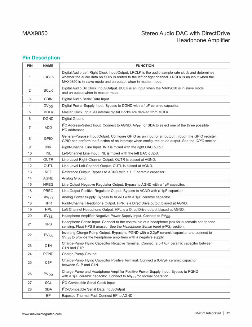
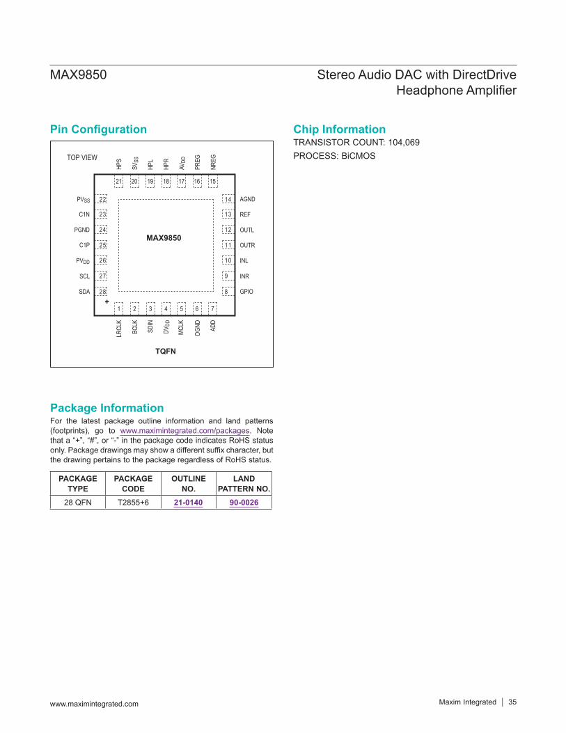
PIN NAME FUNCTION
1 LRCLKDigital Audio Left-Right Clock Input/Output. LRCLK is the audio sample rate clock and determines whether the audio data on SDIN is routed to the left or right channel. LRCLK is an input when the MAX9850 is in slave mode and an output when in master mode.
2 BCLK Digital Audio Bit Clock Input/Output. BCLK is an input when the MAX9850 is in slave mode and an output when in master mode.
3 SDIN Digital Audio Serial Data Input
4 DVDD Digital Power-Supply Input. Bypass to DGND with a 1µF ceramic capacitor.
5 MCLK Master Clock Input. All internal digital clocks are derived from MCLK.
6 DGND Digital Ground
7 ADD I2C Address-Select Input. Connect to AGND, AVDD, or SDA to select one of the three possible I2C addresses.
8 GPIO General-Purpose Input/Output. Configure GPIO as an input or an output through the GPIO register. GPIO can perform the function of an interrupt when configured as an output. See the GPIO section.
9 INR Right-Channel Line Input. INR is mixed with the right DAC output.
10 INL Left-Channel Line Input. INL is mixed with the left DAC output.
11 OUTR Line Level Right-Channel Output. OUTR is biased at AGND.
12 OUTL Line Level Left-Channel Output. OUTL is biased at AGND.
13 REF Reference Output. Bypass to AGND with a 1µF ceramic capacitor.
14 AGND Analog Ground
15 NREG Line Output Negative Regulator Output. Bypass to AGND with a 1µF capacitor.
16 PREG Line Output Positive Regulator Output. Bypass to AGND with a 1µF capacitor.
17 AVDD Analog Power Supply. Bypass to AGND with a 1µF ceramic capacitor.
18 HPR Right-Channel Headphone Output. HPR is a DirectDrive output biased at AGND.
19 HPL Left-Channel Headphone Output. HPL is a DirectDrive output biased at AGND.
20 SVSS Headphone Amplifier Negative Power-Supply Input. Connect to PVSS.
21 HPS Headphone Sense Input. Connect to the control pin of a headphone jack for automatic headphone sensing. Float HPS if unused. See the Headphone Sense Input (HPS) section.
22 PVSSInverting Charge-Pump Output. Bypass to PGND with a 2.2µF ceramic capacitor and connect to SVSS to provide the headphone amplifiers with a negative supply.
23 C1N Charge-Pump Flying Capacitor Negative Terminal. Connect a 0.47µF ceramic capacitor between C1N and C1P.
24 PGND Charge-Pump Ground
25 C1P Charge-Pump Flying Capacitor Positive Terminal. Connect a 0.47µF ceramic capacitor between C1P and C1N.
26 PVDDCharge-Pump and Headphone Amplifier Positive Power-Supply Input. Bypass to PGND with a 1µF ceramic capacitor. Connect to AVDD for normal operation.
27 SCL I2C-Compatible Serial Clock Input
28 SDA I2C-Compatible Serial Data Input/Output
— EP Exposed Thermal Pad. Connect EP to AGND.
Pin Description
MAX9850 Stereo Audio DAC with DirectDrive Headphone Amplifier
www.maximintegrated.com Maxim Integrated 12
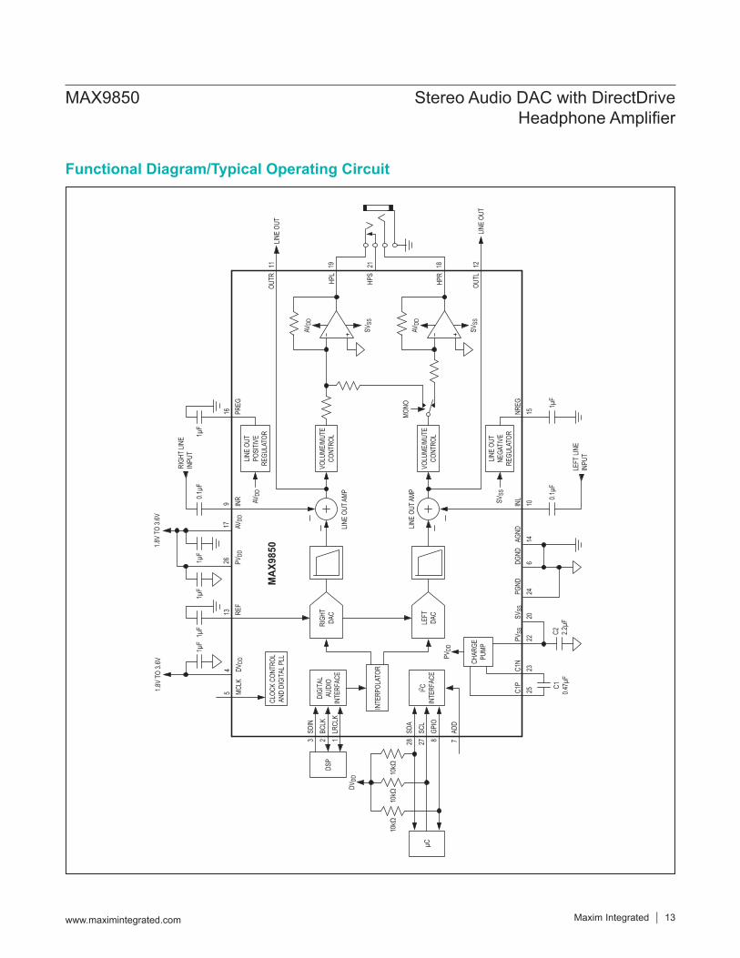
Functional Diagram/Typical Operating Circuit
AVDD
SVSS
AVDD
SVSS
MONO
VOLU
ME/M
UTE
CONT
ROL
LINE
OUT
POSI
TIVE
REGU
LATO
R
LINE
OUT
NEGA
TIVE
REGU
LATO
R
VOLU
ME/M
UTE
CONT
ROL
LINE
OUT A
MP
LINE
OUT A
MP
INTE
RPOL
ATOR
RIGH
TDA
C
LEFT
DAC
MAX
9850
3 2 1
DIGI
TAL
AUDI
OIN
TERF
ACE
DSP
SDIN
BCLK
LRCL
K
28 27 8I2 C
INTE
RFAC
E
SDA
SCL
GPIO
AVDD
SVSS
CLOC
K CO
NTRO
LAN
D DI
GITA
L PLL CH
ARGE
PUMP
PVDD
C1P
C1N
PVSS
SVSS
2523
22PG
NDDG
NDAG
ND24
620
OUTR HP
L
HPS
HPR
OUTL
11 182119 12
LINE
OUT
LINE
OUT
14IN
L10
LEFT
LINE
INPU
T
NREG
15
0.1µF
1µF
C2 2.2µF
C10.4
7µF
ADD
10kΩ
10kΩ
10kΩ
DVDD
µC
1.8V
TO 3.
6V
54
13MC
LKDV
DDRE
F
1µF
26 PVDD
1µF
9 INR
1.8V
TO 3.
6V
17 AVDD
1µF
0.1µF
1µF
16
1µF
PREG
7
RIGH
T LIN
EIN
PUT
MAX9850 Stereo Audio DAC with DirectDrive Headphone Amplifier
www.maximintegrated.com Maxim Integrated 13
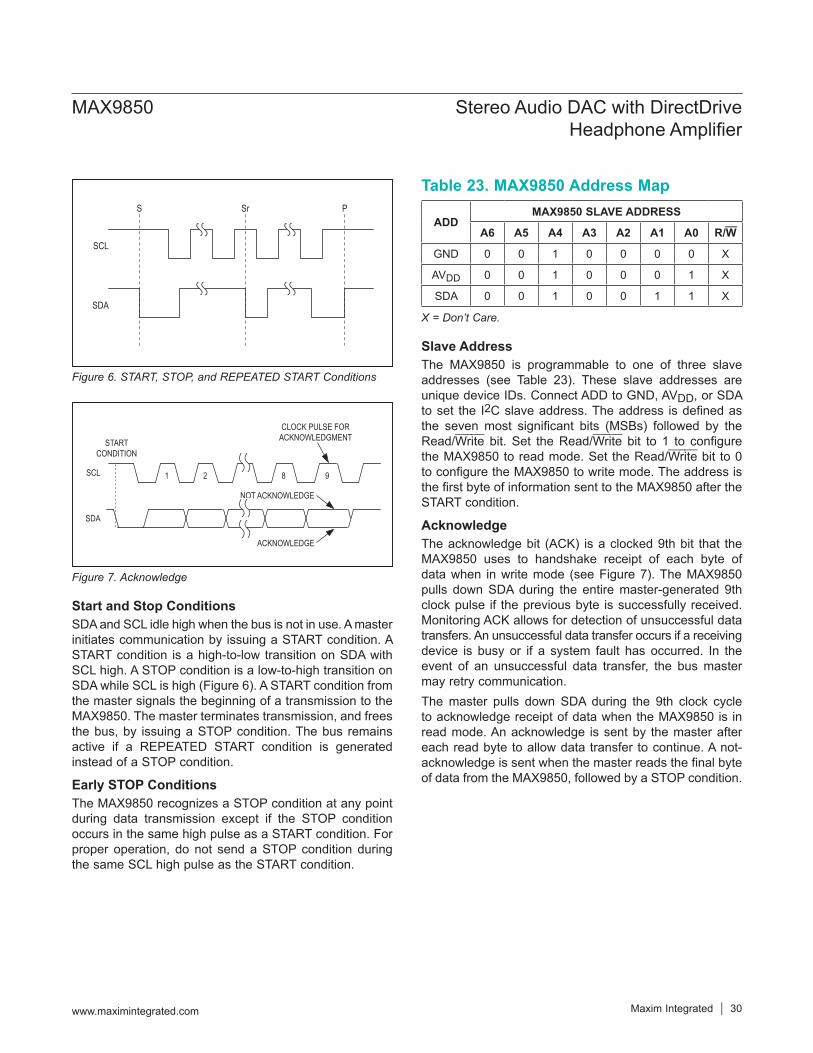
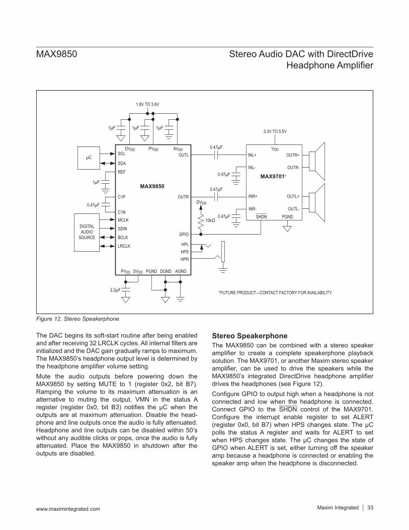
Detailed DescriptionThe MAX9850 audio digital-to-analog converter (DAC) with a stereo DirectDrive headphone amplifier is a complete digital audio playback solution. The sigma-delta DAC has 90dB of dynamic range and accepts stereo audio data at sampling frequencies ranging from 8kHz to 48kHz. Headphone output volume level, muting, and device configuration are programmed through the I2C-compatible interface. Three selectable I2C device IDs are available. Both basic modes of operation, integer and noninteger, provide full dynamic range performance and allow maximum flexibility when choosing the MAX9850’s master clock (MCLK) frequency. Integer mode operation requires that MCLK is an integer multiple of 16 times the sample rate, and provides maximum full-scale SNR performance. Noninteger mode allows maximum flexibility when choosing an MCLK frequency, as the MCLK may be any frequency in the acceptable range.Audio data is sent to the MAX9850 through a 3-wire digital audio data bus that supports numerous input formats. LRCLK and BCLK signals are generated by the MAX9850 when configured in master mode. The MAX9850 can also be configured as a slave device, accepting LRCLK and BCLK signals from an external digital audio master. External LRCLK and BCLK signals may be either synchronous or asynchronous with MCLK when the MAX9850 is configured as a slave device.Maxim’s DirectDrive architecture employs an internal charge pump to create a negative voltage supply to power the headphone amplifier outputs. The internal negative supply allows the analog output signals to be biased at ground, eliminating the need for an output-coupling capacitor, reducing system cost and size.The MAX9850’s stereo line inputs allow mixing of analog audio with digital audio. The summed audio signal is sent directly to the line and headphone outputs. The line inputs/outputs can be activated even when the DAC is disabled and MCLK is not present.The headphone sense input (HPS) detects when a head-phone is connected to the MAX9850. The HPS circuit shuts down the headphone amplifier outputs when no headphones are connected. The headphone amplifiers can be automatically enabled when HPS detects the presence of headphones.
Sigma-Delta DACThe MAX9850 uses a sigma-delta DAC to achieve up to 91dB of SNR. The DAC receives a stereo digital input signal sampled at fLRCLK, interpolates the signal data to an 8 times fLRCLK frequency, and digitally filters the
samples. The resulting oversampled digital signal is then converted using a multibit sigma-delta modulator followed by an analog smoothing filter that greatly attenuates high-frequency quantization noise typical with oversampling converters. Flexible clocking modes allow the MAX9850 to be used effectively in applications normally not well suited for oversampling converters all without the need for expensive sample rate converters.Set DACEN = 0 in the enable register (register 0x5, bit B0) to disable the DAC. Set DACEN = 1 to enable the DAC.
Line Outputs/InputsThe MAX9850 features line inputs (INR, INL) and line outputs (OUTR, OUTL). The line inputs allow a line level signal to be mixed with the DAC output, see the Functional Diagram/Typical Operating Circuit. Set LNIEN = 1 in the enable register (register 0x5, bit B1) to enable the line inputs. The line inputs are biased at AGND and can be directly coupled or AC-coupled to INR and INL, depending on the signal source.Stereo DirectDrive line outputs (OUTR and OUTL) can be used to drive line-level loads. Line outputs internally drive the inputs of the headphone amplifier. Set LNOEN = 1 in the enable register (register 0x5, bit B2) to enable the line outputs. Disabling the line outputs will also disable the headphone outputs.The internal charge pump must be enabled to operate the line outputs. Enable the charge pump by configuring CPEN(1:0) = 11 in the enable register (register 0x5, bit B5 and B4). See the Charge Pump section.
DirectDrive Headphone and Line AmplifiersUnlike the MAX9850, traditional single-supply headphone amplifiers have their outputs biased about a nominal DC voltage, typically half the supply, for maximum dynamic range. Large coupling capacitors are typically needed to block this DC bias from the headphone. Without these capacitors, a significant amount of DC current flows to the headphone, resulting in unnecessary power dissipation and possible damage to both headphone and headphone amplifier.Maxim’s DirectDrive architecture uses a charge pump to create an internal negative supply voltage. This allows the MAX9850 headphone and line outputs to be biased about ground, almost doubling the dynamic range while operating from a single supply. With no DC component, there is no need for the large DC-blocking capacitors. Instead of two large (33µF to 330µF) capacitors, the MAX9850 charge pump requires only two small ceramic
MAX9850 Stereo Audio DAC with DirectDrive Headphone Amplifier
www.maximintegrated.com Maxim Integrated 14
capacitors (0.47µF and 2.2µF), conserving board space, reducing cost, improving the frequency response, and THD of the headphone amplifier. In addition to the cost and size disadvantages, the DC-blocking capacitors required by conventional headphone amplifiers limit low-frequency response and decrease PSRR performance. Some dielectrics can significantly distort the audio signal.
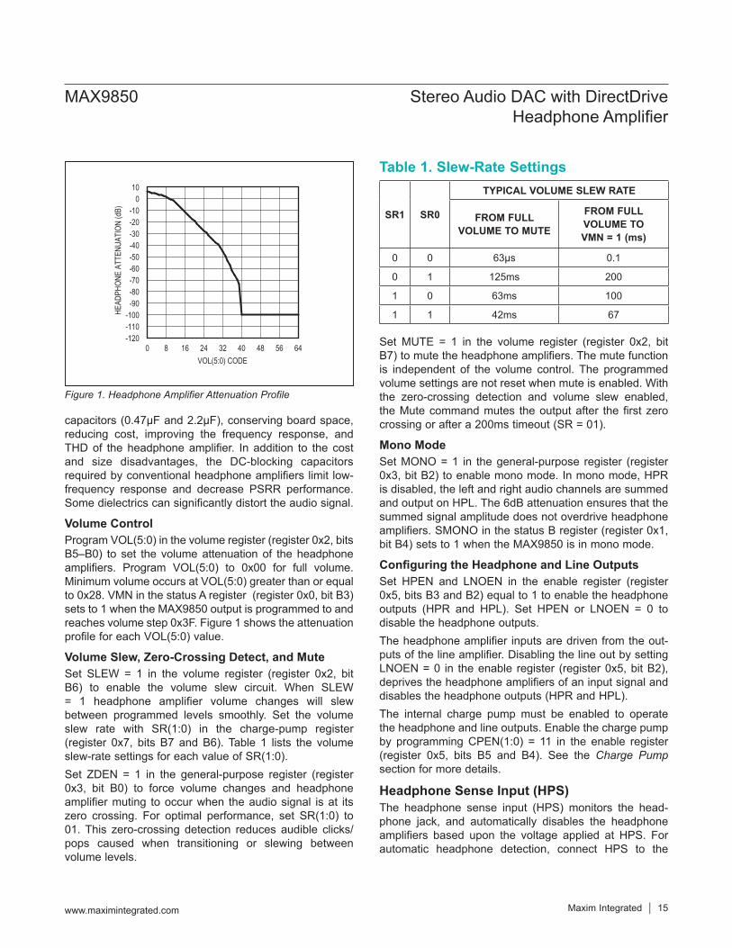
Volume ControlProgram VOL(5:0) in the volume register (register 0x2, bits B5–B0) to set the volume attenuation of the headphone amplifiers. Program VOL(5:0) to 0x00 for full volume. Minimum volume occurs at VOL(5:0) greater than or equal to 0x28. VMN in the status A register (register 0x0, bit B3) sets to 1 when the MAX9850 output is programmed to and reaches volume step 0x3F. Figure 1 shows the attenuation profile for each VOL(5:0) value.
Volume Slew, Zero-Crossing Detect, and MuteSet SLEW = 1 in the volume register (register 0x2, bit B6) to enable the volume slew circuit. When SLEW = 1 headphone amplifier volume changes will slew between programmed levels smoothly. Set the volume slew rate with SR(1:0) in the charge-pump register (register 0x7, bits B7 and B6). Table 1 lists the volume slew-rate settings for each value of SR(1:0).Set ZDEN = 1 in the general-purpose register (register 0x3, bit B0) to force volume changes and headphone amplifier muting to occur when the audio signal is at its zero crossing. For optimal performance, set SR(1:0) to 01. This zero-crossing detection reduces audible clicks/pops caused when transitioning or slewing between volume levels.
Set MUTE = 1 in the volume register (register 0x2, bit B7) to mute the headphone amplifiers. The mute function is independent of the volume control. The programmed volume settings are not reset when mute is enabled. With the zero-crossing detection and volume slew enabled, the Mute command mutes the output after the first zero crossing or after a 200ms timeout (SR = 01).
Mono ModeSet MONO = 1 in the general-purpose register (register 0x3, bit B2) to enable mono mode. In mono mode, HPR is disabled, the left and right audio channels are summed and output on HPL. The 6dB attenuation ensures that the summed signal amplitude does not overdrive headphone amplifiers. SMONO in the status B register (register 0x1, bit B4) sets to 1 when the MAX9850 is in mono mode.
Configuring the Headphone and Line OutputsSet HPEN and LNOEN in the enable register (register 0x5, bits B3 and B2) equal to 1 to enable the headphone outputs (HPR and HPL). Set HPEN or LNOEN = 0 to disable the headphone outputs.The headphone amplifier inputs are driven from the out-puts of the line amplifier. Disabling the line out by setting LNOEN = 0 in the enable register (register 0x5, bit B2), deprives the headphone amplifiers of an input signal and disables the headphone outputs (HPR and HPL).The internal charge pump must be enabled to operate the headphone and line outputs. Enable the charge pump by programming CPEN(1:0) = 11 in the enable register (register 0x5, bits B5 and B4). See the Charge Pump section for more details.
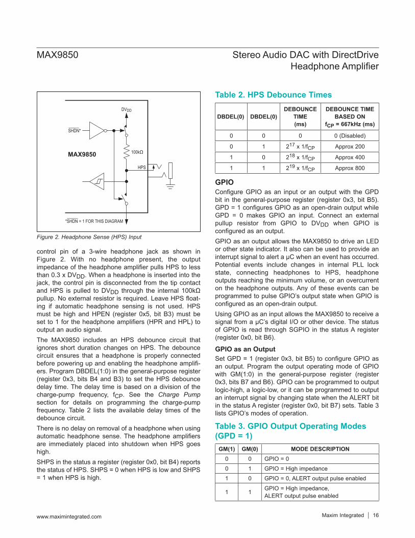
Headphone Sense Input (HPS)The headphone sense input (HPS) monitors the head-phone jack, and automatically disables the headphone amplifiers based upon the voltage applied at HPS. For automatic headphone detection, connect HPS to the
Figure 1. Headphone Amplifier Attenuation Profile
Table 1. Slew-Rate Settings
SR1 SR0
TYPICAL VOLUME SLEW RATE
FROM FULL VOLUME TO MUTE
FROM FULL VOLUME TOVMN = 1 (ms)
0 0 63µs 0.1
0 1 125ms 200
1 0 63ms 100
1 1 42ms 67
VOL(5:0) CODE
HEAD
PHON
E AT
TENU
ATIO
N (d
B)
564832 4016 248
-110-100
-90-80-70-60-50-40-30-20-10
010
-1200 64
MAX9850 Stereo Audio DAC with DirectDrive Headphone Amplifier
www.maximintegrated.com Maxim Integrated 15
control pin of a 3-wire headphone jack as shown in Figure 2. With no headphone present, the output impedance of the headphone amplifier pulls HPS to less than 0.3 x DVDD. When a headphone is inserted into the jack, the control pin is disconnected from the tip contact and HPS is pulled to DVDD through the internal 100kΩpullup. No external resistor is required. Leave HPS float-ing if automatic headphone sensing is not used. HPS must be high and HPEN (register 0x5, bit B3) must be set to 1 for the headphone amplifiers (HPR and HPL) to output an audio signal.The MAX9850 includes an HPS debounce circuit that ignores short duration changes on HPS. The debounce circuit ensures that a headphone is properly connected before powering up and enabling the headphone amplifi-ers. Program DBDEL(1:0) in the general-purpose register (register 0x3, bits B4 and B3) to set the HPS debounce delay time. The delay time is based on a division of the charge-pump frequency, fCP. See the Charge Pump section for details on programming the charge-pump frequency. Table 2 lists the available delay times of the debounce circuit.There is no delay on removal of a headphone when using automatic headphone sense. The headphone amplifiers are immediately placed into shutdown when HPS goes high.SHPS in the status a register (register 0x0, bit B4) reports the status of HPS. SHPS = 0 when HPS is low and SHPS = 1 when HPS is high.
GPIOConfigure GPIO as an input or an output with the GPD bit in the general-purpose register (register 0x3, bit B5). GPD = 1 configures GPIO as an open-drain output while GPD = 0 makes GPIO an input. Connect an external pullup resistor from GPIO to DVDD when GPIO is configured as an output.GPIO as an output allows the MAX9850 to drive an LED or other state indicator. It also can be used to provide an interrupt signal to alert a µC when an event has occurred. Potential events include changes in internal PLL lock state, connecting headphones to HPS, headphone outputs reaching the minimum volume, or an overcurrent on the headphone outputs. Any of these events can be programmed to pulse GPIO’s output state when GPIO is configured as an open-drain output.Using GPIO as an input allows the MAX9850 to receive a signal from a µC’s digital I/O or other device. The status of GPIO is read through SGPIO in the status A register (register 0x0, bit B6).
GPIO as an OutputSet GPD = 1 (register 0x3, bit B5) to configure GPIO as an output. Program the output operating mode of GPIO with GM(1:0) in the general-purpose register (register 0x3, bits B7 and B6). GPIO can be programmed to output logic-high, a logic-low, or it can be programmed to output an interrupt signal by changing state when the ALERT bit in the status A register (register 0x0, bit B7) sets. Table 3 lists GPIO’s modes of operation.
1 1 GPIO = High impedance, ALERT output pulse enabled
DVDD
100kΩ
SHDN*
HPS
MAX9850
*SHDN = 1 FOR THIS DIAGRAM
MAX9850 Stereo Audio DAC with DirectDrive Headphone Amplifier
www.maximintegrated.com Maxim Integrated 16
The interrupt enable register programs the MAX9850 to set ALERT = 1 when an event occurs. GPIO pulses when ALERT sets if GM(1:0) is programmed with 10 or 11. Table 4 contains a list of events that can set ALERT and their corresponding bit positions in the interrupt enable register. Enable the interrupt for each event by setting its bit to 1.
GPIO as an InputThe state of the GPIO input is read through SGPIO in the status A register (register 0x0, bit B6). Set ISGPIO = 1 to allow ALERT to set when SGPIO changes state.
Internal TimingThe internal clock (ICLK) and sample rate clock (LRCLK in master mode) are derived from MCLK. The MAX9850’s flexible operating modes allow any desired LRCLK sample rate to operate over a wide range of MCLK input frequencies.Figure 3 shows a flowchart detailing how the internal clocks are derived from MCLK. The MAX9850 generates ICLK by dividing the MCLK frequency. Higher ICLK frequencies allow for greater DAC oversampling and SNR performance. Dynamic range of 90dB (typ) is possible when fICLK is greater than or equal to 12MHz. Lower ICLK frequencies may require slightly less supply current but sacrifice dynamic range. See the SNR vs. MCLK Frequency graph in the Typical Operating Characteristics.ICLK is a frequency-scaled version of MCLK that is used by the MAX9850 to clock the internal DAC circuitry and generate LRCLK and BCLK when in master mode. The charge-pump clock is derived from ICLK when the internal charge-pump oscillator is not used.Connect an available system clock to MCLK, see the DAC Operating Modes section. MCLK can be supplied from any synchronous or available asynchronous system clock whose frequency falls within the 8.448MHz to 13MHz, or 16.896MHz to 40MHz range. Any MCLK within these ranges allow the MAX9850 to operate at any sample rate between 8kHz to 48kHz in either a master or slave mode of operation. Other MCLK frequencies can still be used, but will limit the sample rate ranges that the MAX9850 operates with as illustrated in Table 5.
Higher ICLK frequencies provide higher SNR. Always use the highest acceptable ICLK. Sample rates other than those listed in Table 5 can be used. The MAX9850 defaults to IC(1:0) = 0x0 at power-up.
DAC Operating ModesFour DAC operating modes: master integer, slave integer, master noninteger, and slave noninteger allow flexibility for operating with various applications and virtually any available MCLK frequency within the system. The operating modes are set with MAS in the digital audio register (register 0xA, bit B7) and INT in the LRCLK MSB register (register 0x8, bit B7). Table 6 shows the four modes of operation and the equations needed to program the MAX9850 to use the DAC modes.The master and slave integer modes are the modes in which DACs commonly operate. In these modes, LRCLK is ICLK divided by an integer value. A typical application would set MCLK equal to 256 x LRCLK. The MAX9850 requires that ICLK be an integer multiple of 16 x LRCLK where the integer multiple is at least 10 when in master or slave integer modes. Integer mode always provides the maximum full-scale signal level performance compared to other modes of operation. Choose integer mode over any other mode of operation when possible.The master noninteger mode allows for a condition where LRCLK and ICLK may not be related by an integer value. In these modes, the MAX9850 can operate from any available MCLK in the system.
Figure 3. Internally Generated Clock Signals Derived from MCLK
Table 4. Interrupt Enable Register (0x4) EventsEVENT BIT NUMBER IN REGISTER 0x4
LCK (register 0x0, bit B5) sets when the internal PLL acquires or loses frequency lock B5
SHPS (register 0x0, bit B4) sets after the headphone is inserted and the debounce time has elapsed when the headphone amplifier is powered up and ready B4
VMN (register 0x0, bit B3) sets when the headphone amplifier minimum volume is reached B3IOHL or IOHR (register 0x0, bits B1 or B0) sets after an overcurrent at either HPL or HPR B0
IC(1:0)0x0 = 1/10x1 = 1/20x2 = 1/30x3 = 1/4
CP(4:0)
LRCLK DIVIDER
INTERNAL CLOCK(ICLK)MASTER CLOCK
(MCLK)CHARGE-PUMPCLOCK
LRCLK**LRCLK IS GENERATED WHEN IN MASTERMODE ONLY. THE DIVIDER IS SET WITH THELRCLK MSB AND LRCLK LSB REGISTERS.
MAX9850 Stereo Audio DAC with DirectDrive Headphone Amplifier
www.maximintegrated.com Maxim Integrated 17
*The first frequency listed is the minimum MCLK frequency required to operate in integer mode. The range of frequencies indicates the MCLK frequencies the MAX9850 needs to operate in any mode.
Table 5. Acceptable MCLK Frequency Ranges
Table 6. DAC Operating Modes
LRCLK(kHz)
MINIMUM ICLK(MHz)
MAXIMUM ICLK(MHz)
ACCEPTABLE MCLK FREQUENCIES*(MHz)
INTEGER MODE(160 x fLRCLK)
NONINTEGER MODE(176 x fLRCLK) ANY MODE IC(1:0) = 0x0
SF = 1IC(1:0) = 0x1
SF = 2IC(1:0) = 0x2
SF = 3IC(1:0) = 0x3
SF = 4
8 1.280 1.4080 13.0 1.280 and 1.4080 to 13.0
2.560 and 2.8160 to 26.0
3.840 and 4.2240 to 39.0
5.120 and 5.6320 to 40.0
11.025 1.764 1.9404 13.0 1.764 and 1.9404 to 13.0
3.528 and 3.8808 to 26.0
5.292 and 5.8212 to 39.0
7.056 and 7.7616 to 40.0
12 1.920 2.1120 13.0 1.920 and 2.1120 to 13.0
3.840 and 4.2240 to 26.0
5.760 and 6.3360 to 39.0
7.680 and 8.4480 to 40.0
16 2.560 2.8160 13.0 2.560 and 2.8160 to 13.0
5.120 and 5.6320 to 26.0
7.680 and 8.4480 to 39.0
10.240 and 11.2640 to 40.0
22.05 3.528 3.8808 13.0 3.528 and 3.8808 to 13.0
7.056 and 7.7616 to 26.0
10.584 and 11.6424 to 39.0
14.112 and 15.5232 to 40.0
24 3.840 4.2240 13.0 3.840 and 4.2240 to 13.0
7.680 and 8.4480 to 26.0
11.520 and 12.6720 to 39.0
15.360 and 16.8960 to 40.0
32 5.120 5.6320 13.0 5.120 and 5.6320 to 13.0
10.240 and 11.2640 to 26.0
15.360 and 16.8960 to 39.0
20.480 and 22.5280 to 40.0
44.1 7.056 7.7616 13.0 7.056 and 7.7616 to 13.0
14.112 and 15.5232 to 26.0
21.168 and 23.2848 to 39.0
28.224 and 31.0464 to 40.0
48 7.680 8.4480 13.0 7.680 and 8.4480 to 13.0
15.360 and 16.8960 to 26.0
23.040 and 25.3440 to 39.0
30.720 and 33.7920 to 40.0
MODE
SLAVE MODE (MAS = 0)
MASTER MODE (MAS = 1)
LRCLK and BCLK signals supplied from external source
LRCLK and BCLK signals supplied by MAX9850
NONINTEGER MODE (INT = 0)
LRCLK may be any frequency within an acceptable range
Asynchronous Asynchronous
NMSB,LSB = 022
LRCLKMSB,LSB
ICLK
2 fN
f×
=
INTEGER MODE(INT = 1)
ICLK and LRCLK must be synchronous and exact integer ratio related
Synchronous
ICLKLSB MSB
LRCLK
fN , N 0
16 f= =
×
MAX9850 Stereo Audio DAC with DirectDrive Headphone Amplifier
www.maximintegrated.com Maxim Integrated 18
Slave modes of operation allow the MAX9850 to operate in any audio system where the LRCLK and BCLK must be supplied from an external source. When operating in slave mode, the MCLK supplied to the MAX9850 may be either synchronous or asynchronous with LRCLK. Use the slave integer mode if ICLK is synchronous and has an integer multiple of 16 x LRCLK. Integer mode ensures that the highest levels of full-scale-input signal performance can be achieved. Slave noninteger mode offers the highest degree of clock flexibility. ICLK does not need to be synchronous or an integer multiple of LRCLK when operating in slave noninteger mode.Master modes of operation allow the MAX9850 to generate and supply an LRCLK and BCLK to other elements in the system. Use master integer mode if the provided ICLK is an integer multiple of 16 x LRCLK. Integer mode ensures that the highest levels of full-scale input signal performance can be achieved. Master noninteger mode allows the MAX9850 to supply virtually any frequency LRCLK with an accuracy better than ±0.5%.The slave noninteger mode provides maximum flexibility for ICLK and LRCLK frequencies. The ICLK and LRCLK can be asynchronous and noninteger related. Connect any available system clock that is listed on Table 5 in the Internal Timing section. In slave noninteger mode, the acceptable MCLK frequency range is the same as master mode.
Master Integer Mode (MAS = 1, IM = 1)The MAX9850 generates the LRCLK and BCLK in master mode. LRCLK is an integer factor of ICLK by the following equation:
ICLKLRCLK
LSB
ff
16 N=
×
where:fICLK = ICLK frequency. fICLK must be at least 160 x fLRCLK for proper DAC operation.NLSB = decimal value of the data contained in LSB(7:0) (register 0x9, bits B7–B0).fLRCLK = LRCLK frequency.For example:fICLK = 12.228MHz and NLSB = 16 (0x10), fLRCLK = 48kHz.Solve the above equation for NLSB. Use master integer mode if NLSB is an integer. Use master noninteger mode if NLSB is not an integer.
Slave Integer Mode (MAS = 0, IM = 1)The MAX9850 accepts LRCLK and BCLK from an external digital audio source when in slave integer mode. LRCLK must be an exact integer multiple of ICLK to ensure proper operation. Program LSB(7:0) (register 0x9, bits B7–B0) with the LRCLK division ratio. Use the following equation to find the value that needs to be programmed to LSB(7:0):
ICLKLSB
LRCLK
fN
16 f=
×
where:fICLK = ICLK frequency. fICLK must be 160 x fLRCLK for proper DAC operation.fLRCLK = supplied LRCLK frequency.NLSB = decimal value of the data contained in LSB(7:0) (register 0x9, bits B7–B0).For example:fICLK = 11.2896MHz and fLRCLK = 44.1kHz, NLSB = 16 (0x10).Solve the above equation for NLSB. Use slave integer mode if NLSB is an integer. Use slave noninteger mode if NLSB is not an integer.Slave Noninteger (MAS = 0, IM = 0)In slave noninteger mode, the MAX9850 accepts an external LRCLK and converts the digital audio signal using any asynchronous ICLK within the acceptable operating range. The MAX9850 uses internal clock recovery circuitry to generate all required internal clocks. This allows the MAX9850 to operate in systems that do not have dedicated clock sources or crystal oscillators. Virtually any existing system clock will work. fICLK must be at least 176 x fLRCLK for proper operation.
Master Noninteger Mode (MAS = 1, IM = 0)The ICLK frequency in some applications may not be an integer multiple of the desired LRCLK frequency. The MAX9850, operating in master noninteger mode, can generate and output any LRCLK frequency between 8kHz to 48kHz (±0.5%) with any ICLK frequency within the acceptable operating range. In this mode, the MAX9850 generates LRCLK by dividing MCLK by the ratio programmed into MSB(14:8) and LSB(7:0) (register 0x8, bits B7–B0 and register 0x9, bits B6–B0). The LRCLK sample frequency can have any noninteger relationship with respect to MCLK. Calculate the values for MSB(14:8) and LSB(7:0) with the following equation:
22LRCLK
MSB,LSBICLK
22 fN ROUND
f
× =
MAX9850 Stereo Audio DAC with DirectDrive Headphone Amplifier
www.maximintegrated.com Maxim Integrated 19
where:fICLK = ICLK frequency. fICLK must be at least 176 x fLRCLK for proper DAC operation.fLRCLK = LRCLK frequency.NMSB,LSB = decimal value of MSB(14:8) and LSB(7:0) (register 0x8, bits B6–B0 and register 0x9, bits B7–B0).Round the results of the equation to the nearest integer value.For example:fLRCLK = 44.1kHz, fICLK = 12.288MHz.1) Solve for NMSB,LSB, 15052.8.2) Round result to nearest integer value. 15053.3) Convert to hex, 0x3CD.4) Program MSB(14:8) with the MSB 0x3A and program
LSB(7:0) with the LSB 0xCD).Table 7 provides examples of using master noninteger mode with various MCLK frequencies to generate useful LRCLK frequencies.
Charge PumpThe DirectDrive line and headphone outputs of the MAX9850 require a charge pump to create the internal negative power supply. Set CPEN(1:0) = 11 in the enable register (register 0x5, bits B5 and B4) to turn on the charge pump. The negative charge-pump voltage is established and the audio outputs are ready for use approximately 1.4ms after CPEN is set to 11.
The state of CP(4:0), in the charge-pump register (register 0x7, bits B4–B0), determines whether the charge-pump oscillator is derived from the internal 667kHz oscillator or from MCLK. Set CPEN(1:0) = 11 and set CP(4:0) = 0x00 to enable the internal oscillator. The charge pump runs independent from MCLK when the internal oscillator is enabled allowing the charge pump to operate when the DAC is disabled or when only the line inputs are used. No MCLK is required when only the line inputs are used.The switching frequency of the charge pump is well beyond the audio range and does not interfere with audio signals. The switch drivers utilize techniques that minimize noise generated by turn-on and turn-off transients. Although not typically required, additional high-frequency noise attenuation can be achieved by increasing the size of C2 and the PVDD bypass capacitor (see the Functional Diagram/Typical Operating Circuit).Derive the charge-pump clock from MCLK by programming CP(4:0) to a non-zero value based on the following equation:
MCLKCP( 4:0 )
CP
fN
2 f SF=
× ×
where:fMCLK = MCLK frequency.fCP = charge-pump clock frequency. Ensure fCP = 667kHz ±20% for proper operation.SF = MCLK scale factor. SF is the decimal value of IC(1:0) + 1.NCP(4:0) = rounded decimal value of CP(4:0) (register 0x7, bits B4–B0). NCP(4:0) must be greater than 1 when deriving the charge-pump clock from ICLK.
Table 7. Master Noninteger NMSB,LSB Examples
Note: The N values represent the combined MSB(14:8) and LSB(7:0) values.
MAX9850 Stereo Audio DAC with DirectDrive Headphone Amplifier
www.maximintegrated.com Maxim Integrated 20
For example:fMCLK = 12MHz, SF = 1, and fCP = 666.7kHz, NCP(4:0) = 9.Table 8 shows recommended CP(4:0) values for typical MCLK frequencies.
Registers and Bit DescriptionsEleven internal registers program and report the status of the MAX9850. Table 9 lists all of the registers, their addresses, and power-on-reset state. Registers 0x0 and 0x1 are read-only while all of the other registers are read/write. Register 0xB is reserved for factory testing.
Table 9. Register Map
Table 8. Recommended CP(4:0) Values for Typical MCLK Frequencies
X = Don’t Care.
fMCLK(MHz) CP(4:0) IC(1:0) SF fCP
(kHz)
11.2896 0x08 0x0 1 705.6
12.0000 0x09 0x0 1 666.7
12.2880 0x09 0x0 1 682.7
13.0000 0x0A 0x0 1 650.0
24.0000 0x09 0x1 2 666.7
27.0000 0x07 0x2 3 642.9
REGISTER B7 B6 B5 B4 B3 B2 B1 B0 REGISTERADDRESS
POWER-ON RESET STATE
Status A ALERT SGPIO LCK SHPS VMN 1 IOHL IOHR 0x0 —
Status B X X X SMONO SHP SLO SLI SDAC 0x1 —
Volume MUTE SLEW VOL(5:0) 0x2 0x0C
General Purpose GM(1:0) GPD DBDEL(1:0) MONO 0 ZDEN 0x3 0x00
Digital Audio MAS INV BCINV LSF DLY RTJ WS(1:0) 0xA 0x00
RESERVED 0xB —
MAX9850 Stereo Audio DAC with DirectDrive Headphone Amplifier
www.maximintegrated.com Maxim Integrated 21
Status Registers (0x0, 0x1)
Alert Flag (ALERT)1 = An interrupt event has occurred.0 = No interrupt event has occurred.ALERT is an alert flag that sets when an interrupt event has occurred. The events that can be programmed to set ALERT are as follows:
A change in state on SGPIO indicating a change in levels at GPIO when GPIO is configured as an input. Configure GPIO as an input and set ISGPIO = 1 in the interrupt enable register (register 0x4, bit B6).
The internal PLL locks or unlocks with LRCLK. Set ILCK = 1 in the interrupt enable register (register 0x4, bit B5).
A change in state on SHPS indicating headphones have been connected or disconnected. Set ISHPS = 1 in the interrupt enable register (register 0x4, bit B4).
The headphone amplifier reaches its minimum volume. Set IVMN = 1 in the interrupt enable register (register 0x4, bit B3).
An overload on either right or left headphone outputs (HPR, HPL). Set IIOH = 1 in the interrupt enable register (register 0x4, bit B0).
ALERT sets to 1 after an event occurs and remains set until the status A register is read. GPIO configured as an output can interrupt a µC on an ALERT event. GM(1:0) in the GPIO register (register 0x3, bits B7 and B6) control the output mode of GPIO. See the GPIO section for more information on programming GPIO as an output.
GPIO Status (SGPIO)1 = GPIO is high.0 = GPIO is low.SGPIO reports the status of GPIO at the time that status A is read, regardless of whether GPIO is programmed as an input or output. A change in state on SGPIO causes ALERT to set to 1 when GPIO is configured as an input and ISGPIO = 1 in the interrupt enable register (register 0x4, bit B6).
PLL Lock Status (LCK)1 = The internal PLL is locked with LRCLK.0 = The internal PLL is not locked with LRCLK.LCK reports the lock status of the internal PLL at the time that STATUS A is read. The DAC is disabled when the PLL is not locked. When the PLL is locked with LRCLK, the DAC will become operational if DACEN is equal to 1 (register 0x5, bit B0). ALERT sets to 1 when LCK changes state if ILCK = 1 in the interrupt enable register (register 0x4, bit B5).
HPS Status (SHPS)1 = HPS is high, indicating that headphones are connected.0 = HPS is low, indicating no headphone is connected.SHPS reports the debounced status of HPS at the time STATUS A is read. SHPS = 0 indicates that no headphone is connected and HPS is low. SHPS sets to 1 when HPS is high, indicating headphones are connected. ALERT sets to 1 when SHPS changes state, if ISHPS = 1 in the interrupt enable register (register 0x4, bit B4).
Volume at Minimum (VMN)1 = Headphone volume has reached its minimum volume.0 = Headphone volume is not at its minimum.VMN sets to 1 when the minimum headphone amplifier volume has been reached. ALERT sets to 1 when IVMN = 1 in the interrupt enable register (register 0x4, bit B3).
Headphone Overcurrent Left (IOHL)1 = The left headphone output (HPL) has experienced an overcurrent condition.0 = The left headphone output (HPL) is operating normally.IOHL sets to 1, when an overcurrent occurs on the left headphone output HPL and remains set until status a is read. ALERT sets to 1 when an overcurrent on the right or left headphone output occurs if IIOH = 1 in the interrupt enable register (register 0x4, bit B0).
Headphone Overcurrent Right (IOHR)1 = The right headphone output (HPR) has experienced an overcurrent condition.0 = The right headphone output (HPR) is operating normally.IOHR sets to 1 and remains set until STATUS A is read. ALERT sets to 1 when an overcurrent on the right or left headphone output occurs if IIOH = 1 in the interrupt enable register (register 0x4, bit B0).
Table 10. Status A (0x0) Read-Only, Bit Descriptions
B7 B6 B5 B4 B3 B2 B1 B0
ALERT SGPIO LCK SHPS VMN 1 IOHL IOHR
MAX9850 Stereo Audio DAC with DirectDrive Headphone Amplifier
www.maximintegrated.com Maxim Integrated 22
Mono Status (SMONO)1 = The headphone amplifier outputs are in mono mode.0 = The headphone amplifier outputs are in stereo mode.SMONO indicates whether the headphone outputs are in mono or stereo mode. In mono mode, the left and right audio signals are mixed and output to the left headphone output. Set MONO = 1 in the general-purpose register (register 0x3, bit B2) to enter mono mode.
Headphone Amplifier Status (SHP)0 = The headphone amplifiers are operating.1 = The headphone amplifiers are not operating.SHP indicates whether the headphone amplifiers are operating or not operating.
Line Output Status (SLO)0 = The line outputs are enabled.1 = The line outputs are disabled.SLO indicates whether the line outputs are enabled or disabled. Set LNOEN = 1 in the enable register (register 0x5, bit B2) to enable the line outputs.
Line Input Status (SLI)0 = The line inputs are enabled.1 = The line inputs are disabled.SLI indicates whether the line inputs are enabled or disabled. Set LNIEN = 1 in the enable register (register 0x5, bit B1) to enable the line inputs.
DAC Status (SDAC)0 = The DAC is operating and has completed a soft-start sequence.1 = The DAC is not operating and has completed a soft-stop sequence.SDAC indicates whether the DAC is operational and receiving valid clock signals, or not operating.
Table 11. Status B (0x1) Read-Only, Bit Descriptions
B7 B6 B5 B4 B3 B2 B1 B0
X X X SMONO SHP SLO SLI SDAC
MAX9850 Stereo Audio DAC with DirectDrive Headphone Amplifier
www.maximintegrated.com Maxim Integrated 23
Volume Register (0x2)
Mute Enable (MUTE)1 = Mute headphone outputs.0 = Unmute headphone outputs.Set MUTE = 1 to mute the headphone outputs (HPR, HPL). The headphone output is muted on the first zero crossing of the audio signal if zero-crossing detect is enabled.
Slew-Rate Control Enable (SLEW)1 = Enable slew-rate control.0 = Disable slew-rate control.The slew-rate control allows the headphone amplifiers to smoothly slew between volume settings after a volume change is made. Volume changes occur immediately when the slew-rate control is disabled.
Volume Control (VOL(5:0))VOL(5:0) controls the headphone amplifier volume attenuation. Code 0x00 is full volume while 0x28 to 0x3F is full attenuation. VMN sets to 1 when code 0x3F is programmed and the minimum volume is reached. Table 13 lists the volume attenuation settings for each code.
Table 12. Volume (0x2) Read/Write, Bit Descriptions
MAX9850 Stereo Audio DAC with DirectDrive Headphone Amplifier
www.maximintegrated.com Maxim Integrated 24
General-Purpose Register
GPIO Output Mode Control (GM(1:0))00 = GPIO outputs low.01 = GPIO is high impedance.10 = GPIO outputs low and the ALERT output pulse function is enabled.11 = GPIO is high impedance and the ALERT output pulse function is enabled.GM(1:0) programs the GPIO output state and enables or disables the ALERT output pulse function. The open-drain GPIO output can be programmed to output static high or a low. GPIO can also be programmed to pulse to the opposite output level than the programmed output state when an alert occurs. An alert occurs when ALERT sets to 1 in the status A register. GM(1:0) has no function when GPIO is configured as an input.
GPIO Direction (GPD)1 = Configure GPIO as an open-drain output.0 = Configure GPIO as an input.The state of GPD determines whether GPIO is an input or an output.Debounce Delay Control (DBDEL(1:0))00 = HPS debounce delay disabled.01 = HPS debounce delay is a nominal 200ms.10 = HPS debounce delay is a nominal 400ms.11 = HPS debounce delay is a nominal 800ms.DBDEL(1:0) controls the length of HPS debounce time. The debounce time is derived from the charge-pump clock.Mono Mode Enable (MONO)1 = Enable mono mode.0 = Disable mono mode, headphone outputs in stereo mode.Set MONO = 1 to force the headphone outputs to mono mode. The stereo input signal is summed to one channel. The summed signal is output on the left headphone output (HPL).
Zero-Detect Enable (ZDEN)1 = Enables the zero-detect function.0 = Disables the zero-detect function.
Volume changes, headphone output muting, and entering/exiting shutdown occur only on the zero crossing of the audio signal when ZDEN = 1. For optimum performance, set SR(1:0) to 01.
Interrupt Enable Register
Note: Any of the below interrupts can be configured to trigger a hardware interrupt through GPIO. Program GPD and GM(1:0) in the general-purpose register to enable the ALERT output pulse function.
SGPIO Interrupt Enable (ISGPIO)1 = A state change on SGPIO, when GPIO is an input, will cause ALERT to set to 1.0 = A state change on SGPIO, when GPIO is an input, will not cause ALERT to set.ISGPIO = 1 configures the MAX9850 to set ALERT = 1 when SGPIO changes state. The interrupt may only be enabled when GPIO is an input.
PLL Lock Interrupt Enable (ILCK)1 = A state change on LCK will cause ALERT to set to 1.0 = A state change on LCK will not cause ALERT to set.ILCK = 1 configures the MAX9850 to set ALERT = 1 when the DAC’s internal PLL loses or achieves frequency lock with LRCLK. Program GM(1:0), while GPD = 1, to configure GPIO as a hardware interrupt to alert a µC when LCK changes state.
SHPS Interrupt Enable (ISHPS)1 = A state change on SHPS will cause ALERT to set to 1.0 = A state change on SHPS will not cause ALERT to set.ISHPS = 1 configures the MAX9850 to set ALERT = 1 when SHPS changes state.
Volume at Minimum Interrupt Enable (IVMN)1 = A state change on VMN will cause ALERT to set to 1.0 = A state change on VMN will not cause ALERT to set.IVMN = 1 configures the MAX9850 to set ALERT = 1 when the headphone amplifier is programmed to and reaches its minimum output volume. Program GM(1:0), while GPD = 1, to configure GPIO as a hardware interrupt to alert a µC when the headphone output volume is programmed to and reaches its minimum volume.
Table 14. General Purpose (0x3) Read/Write, Bit Descriptions
Table 15. Interrupt Enable (0x4) Read/Write, Bit Descriptions
B7 B6 B5 B4 B3 B2 B1 B0
GM(1:0) GPD DBDEL(1:0) MONO 0 ZDEN
B7 B6 B5 B4 B3 B2 B1 B0
0 ISGPIO ILCK ISHPS IVMN 0 0 IIOH
MAX9850 Stereo Audio DAC with DirectDrive Headphone Amplifier
www.maximintegrated.com Maxim Integrated 25
Headphone Overcurrent Interrupt Enable (IIOH)1 = ALERT sets to 1 when either IOHL or IOHR set to 1.0 = ALERT will not set when IOHL or IOHR set to 1.IIOH = 1 configures the MAX9850 to set ALERT = 1 when one or both of the headphone amplifier outputs (HPL, HPR) has experienced an overcurrent condition. Program GM(1:0), while GPD = 1, to configure GPIO as a hardware interrupt to alert a µC to an overcurrent condition on the headphone outputs.
Enable Register
Shutdown (SHDN)1 = The MAX9850 is powered on.0 = The MAX9850 is in low-power shutdown mode. The I2C interface remains active.Set SHDN = 1 to power on the MAX9850. The headphone amplifier, master clock, line inputs/outputs, DAC, charge pump, and charge-pump clock all have their own enable bits. The individual components of the MAX9850 can only be enabled after SHDN = 1.
MCLK Enable (MCLKEN)1 = MCLK is connected to the MAX9850.0 = MCLK is disconnected from the MAX9850.MCLKEN must be set to 1 for the DAC to operate properly. The line inputs/outputs and headphone amplifiers will work if MCLKEN = 0, but the charge-pump clock must be derived from the internal oscillator.
Charge-Pump Enable (CPEN(1:0))11 = Enable the internal charge pump.00 = Disable the internal charge pump.10 and 01 = Invalid.Set CPEN(1:0) to 11 to enable the internal charge pump when the line outputs and headphone amplifiers are used.
Headphone Output Enable (HPEN)1 = Enable the headphone outputs.0 = Disable the headphone outputs.Set HPEN = 1 to enable the headphone outputs. HPEN = 0 places the headphone outputs in high impedance. The line outputs must be enabled for the headphone amplifiers to operate properly.
Line Output Enable (LNOEN)1 = Enable the line outputs.0 = Disable the line outputs.LNOEN = 0 forces the line outputs and the headphone outputs to high impedance. Set LNOEN = 1 to enable the line outputs. The line outputs must be enabled for the headphone amplifiers to operate properly.
Line Input Enable (LNIEN)1 = Enable the line inputs.0 = Disable the line inputs.LNIEN = 1 enables the line inputs. LNIEN = 0 disconnects the line inputs.
DAC Enable (DACEN)1 = Enable the audio DAC.0 = Disable the audio DAC.DACEN = 1 enables the DAC and all supporting circuitry including the digital audio interface and interpolating FIR filter. DACEN = 0 places the DAC and support circuitry into low-power shutdown mode.
Clock Register
Internal Clock Divide (IC(1:0))00 = Internal clock divider is transparent (fICLK = fMCLK).01 = (fICLK = fMCLK / 2).10 = (fICLK = fMCLK / 3).11 = (fICLK = fMCLK / 4).IC(1:0) controls the internal clock divider that determines the internal clock frequency from the master clock.
Charge-Pump Register
Table 16. Enable (0x5) Read/Write, Bit Descriptions
Table 17. Clock (0x6) Read/Write, Bit Descriptions
Table 18. Charge Pump (0x7) Read/Write, Bit Descriptions
B7 B6 B5 B4 B3 B2 B1 B0
SHDN MCLKEN CPEN (1:0) HPEN LNOEN LNIEN DACEN
B7 B6 B5 B4 B3 B2 B1 B0
0 0 0 0 IC(1:0) 0 0
B7 B6 B5 B4 B3 B2 B1 B0
SR(1:0) 0 CP(4:0)
MAX9850 Stereo Audio DAC with DirectDrive Headphone Amplifier
www.maximintegrated.com Maxim Integrated 26
Slew-Rate Control (SR(1:0))00 = Headphone volume slews from code 0x00 to 0x28 in 63µs. Not recommended when ZDEN = 1.01 = Headphone volume slews from code 0x00 to 0x28 in 125ms.10 = Headphone volume slews from code 0x00 to 0x28 in 63ms.11 = Headphone volume slews from code 0x00 to 0x28 in 42ms.Program SR(1:0) to set the rate that the MAX9850 uses to slew between two volume settings. The slew-rate control also controls the amount of time the headphone outputs take to mute or shut down after the command is given.
Charge-Pump Clock Divider (CP(4:0))CP(4:0) controls the charge-pump clock divider. The charge-pump clock frequency (fCPCLK) is derived from either ICLK or from the internal oscillator.Program CP(4:0) = 0x00 to enable the 667kHz internal oscillator. This allows the headphone amplifiers and line outputs to operate when the DAC is disabled.Programming CP(4:0) to any value other than 0x00 disables the internal oscillator and derives the charge-pump clock from ICLK. Program CP(4:0) with a value that creates a 667kHz ±20% charge-pump clock from ICLK by the following equation:
MCLKCP
NCP( 4:0 )
ff
2 SF=
× ×
where:fMCLK = MCLK frequency.NCP(4:0) = decimal value of CP(4:0). NCP(4:0) must be greater than 1 when deriving the charge-pump clock from ICLK.fCP = charge-pump clock frequency. Program fCP = 667kHz ±20% for proper operation. SF = MCLK scale factor. SF is the decimal value of IC(1:0) + 1.
LRCLK MSB and LRCLK LSB Registers
Integer Mode (INT)1 = Configure the MAX9850 to integer mode.0 = Configure the MAX9850 to noninteger mode.Integer mode operation requires that ICLK is an integer multiple of 16 times the sample rate (fLRCLK). See the DAC Operating Modes section. When in integer mode, fLRCLK = fICLK / (16 x LSB(7:0)).
LRCLK MSB Divider (MSB(14:8))MSB(14:8) and LSB(7:0) are used to determine fLRCLK when in noninteger mode only (see the DAC Operating Modes section). For nonintegger mode:
22LRCLK
MSB,LSBICLK
2 fN
f×
=
LRCLK LSB Divider (LSB(7:0))LSB(7:0) combined with MSB(14:8) sets the LRCLK divider when the MAX9850 is configured in noninteger mode. Only LSB(7:0) is used to determine fLRCLK when the MAX9850 is configured in integer mode. See the DAC Operating Modes section.
Digital Audio Register
Master Mode (MAS)1 = Configure the MAX9850 to master mode.0 = Configure the MAX9850 to slave mode.Set MAS = 1 to configure the MAX9850 to master mode. The LRCLK and BCLK are generated by the MAX9850 when in master mode. Set MAS = 0 to configure the MAX9850 as a digital audio slave that accepts LRCLK and BCLK from an external digital audio source.
LRCLK Invert (INV)1 = Left audio data is clocked in when LRCLK is high and right data is clocked in when LRCLK is low.0 = Left audio data is clocked in when LRCLK is low and right data is clocked in when LRCLK is high.Set INV = 0 to conform to the I2S standard.Bit Clock Invert (BCINV)1 = Digital data at SDIN latches in on the falling edge of BCLK.0 = Digital data at SDIN latches in on the rising edge of BCLK.Set BCINV = 0 to conform to the I2S standard.
Table 19. LRCLK MSB (0x8) and LRCLK LSB (0x9) Read/Write, Bit Descriptions
Table 20. Digital Audio (0xA) Read/Write, Bit Descriptions
B7 B6 B5 B4 B3 B2 B1 B0
INT MSB(14:8)
LSB(7:0)
B7 B6 B5 B4 B3 B2 B1 B0
MAS INV BCINV LSF DLY RTJ WS(1:0)
MAX9850 Stereo Audio DAC with DirectDrive Headphone Amplifier
www.maximintegrated.com Maxim Integrated 27
Least Significant Bit First (LSF)1 = Accepts audio data LSB first.0 = Accepts audio data MSB first.Set LSF = 0 to conform to the I2S standard.
SDIN Delay (DLY)1 = Audio data is latched into the MAX9850 on the second rising BCLK edge after LRCLK transitions.0 = Audio data is latched into the MAX9850 on the first rising BCLK edge after LRCLK transitionsSet DLY = 1 to conform to the I2S standard.
Right-Justified Data (RTJ)1 = Audio data is right justified.0 = Audio data is left justified.I2S data is left justified. Set RTJ = 0 to conform to the I2S standard.
Word Length Select (WS(1:0))00 = Audio data word length is 16 bits.01 = Audio data word length is 18 bits.10 = Audio data word length is 20 bits.11 = Audio data word length is 24 bits.Program WS(1:0) to select the input data word length. Programming the audio data word length ensures that the correct number of BCLK cycles are output to accommodate the incoming data word.
Digital Audio InterfaceThe MAX9850 receives serial digital audio data through a 3-wire interface. The data can be right or left justified, MSB or LSB first, or I2S compatible. The 3-wire serial bus carries two time-multiplexed audio data channels (SDIN), a channel-select line (LRCLK), and a bit clock line (BCLK). The configuration of the audio interface is controlled with the digital audio register, see Table 20. Typical digital audio formats, and the required digital audio register code, are listed in Table 21. Figure 4 illustrates the difference between right justified, left justified, and I2S compatible audio data.
The MAX9850 generates the BCLK and the LRCLK from ICLK when in master mode, see the Internal Timing section. In slave mode, the MAX9850 accepts an LRCLK and BCLK from an external digital audio source.
The MAX9850 can accept right- or left-justified data when operating in slave mode with extra BCLK pulses beyond what is programmed by the WS(1:0) bits. When using the I2S standard, audio data MSBit must latch into SDIN on the second BCLK rising edge following an LRCLK transition. See Figure 4 for the various relationships between clock and data that are supported by the MAX9850.The MAX9850 can be configured to accept 16, 18, 20, or 24-bit data. The MAX9850 generates exactly the programmed number of BCLK cycles when in master mode. Program the audio data word size with WS(1:0) (register 0xA, bit B0 and B1) according to Table 22 to ensure that the MAX9850 outputs the correct number of BCLK cycles to accommodate the input word.
The internal digital processing resolution is 18 bits wide. Data words longer than 18 bits will be truncated. Zeros are internally programmed into the missing bit positions when the data word is shorter than the programmed word size.
I2C-Compatible Serial InterfaceThe MAX9850 features an I2C/SMBus™-compatible, 2-wire serial interface consisting of a serial data line (SDA) and a serial clock line (SCL). SDA and SCL facilitate communication between the MAX9850 and the master at clock rates up to 400kHz. Figure 5 shows the 2-wire interface timing diagram. The master generates SCL and initiates data transfer on the bus.A master device writes data to the MAX9850 by transmitting the proper slave address followed by the register address and then the data word. Each transmit sequence is framed by a START (S) or REPEATED START (Sr) condition and a STOP (P) condition. Each word transmitted to the MAX9850 is 8 bits long and is followed by an acknowledge clock pulse.
Table 21. Typical Digital Audio Formats
Table 22. Audio Data Word Size
SMBus is a trademark of Intel Corp.
FORMAT DIGITAL AUDIO REGISTER CODE (0xA)
Left-Justified Audio Data X0000000Right-Justified Audio Data X0000100I2S-Compatible Audio Data X0001000
WS(1:0) DATA WORD SIZE (BITS)
0x0 16
0x1 18
0x2 20
0x3 24
MAX9850 Stereo Audio DAC with DirectDrive Headphone Amplifier
www.maximintegrated.com Maxim Integrated 28
A master reading data from the MAX9850 transmits the proper slave address followed by a series of nine SCL pulses. The MAX9850 transmits data on SDA in sync with the master-generated SCL pulses. The master acknowl-edges receipt of each byte of data. Each read sequence is framed by a START or REPEATED START condition, a not acknowledge, and a STOP condition.SDA operates as both an input and an open-drain output. Apullupresistor,typicallygreaterthan500Ω,isrequiredon the SDA bus. SCL operates as an input only. A pullup resistor, typicallygreater than500Ω, is requiredonSCLif there are multiple masters on the bus, or if the master
in a single-master system has an open-drain SCL output. Series resistors in line with SDA and SCL are optional. Series resistors protect the digital inputs of the MAX9850 from high-voltage spikes on the bus lines, and minimize crosstalk and undershoot of the bus signals.
Bit TransferOne data bit is transferred during each SCL cycle. The data on SDA must remain stable during the high period of the SCL pulse. Changes in SDA while SCL is high are control signals (see the START and STOP Conditions sec-tion). SDA and SCL idle high when the I2C bus is not busy.
Figure 4. Right-Justified, and Left-Justified Audio Data Formats (Slave Mode, 16-Bit Data)
MAX9850 Stereo Audio DAC with DirectDrive Headphone Amplifier
www.maximintegrated.com Maxim Integrated 29
Start and Stop ConditionsSDA and SCL idle high when the bus is not in use. A master initiates communication by issuing a START condition. A START condition is a high-to-low transition on SDA with SCL high. A STOP condition is a low-to-high transition on SDA while SCL is high (Figure 6). A START condition from the master signals the beginning of a transmission to the MAX9850. The master terminates transmission, and frees the bus, by issuing a STOP condition. The bus remains active if a REPEATED START condition is generated instead of a STOP condition.
Early STOP ConditionsThe MAX9850 recognizes a STOP condition at any point during data transmission except if the STOP condition occurs in the same high pulse as a START condition. For proper operation, do not send a STOP condition during the same SCL high pulse as the START condition.
Slave AddressThe MAX9850 is programmable to one of three slave addresses (see Table 23). These slave addresses are unique device IDs. Connect ADD to GND, AVDD, or SDA to set the I2C slave address. The address is defined as the seven most significant bits (MSBs) followed by the Read/Write bit. Set the Read/Write bit to 1 to configure the MAX9850 to read mode. Set the Read/Write bit to 0 to configure the MAX9850 to write mode. The address is the first byte of information sent to the MAX9850 after the START condition.
AcknowledgeThe acknowledge bit (ACK) is a clocked 9th bit that the MAX9850 uses to handshake receipt of each byte of data when in write mode (see Figure 7). The MAX9850 pulls down SDA during the entire master-generated 9th clock pulse if the previous byte is successfully received. Monitoring ACK allows for detection of unsuccessful data transfers. An unsuccessful data transfer occurs if a receiving device is busy or if a system fault has occurred. In the event of an unsuccessful data transfer, the bus master may retry communication.The master pulls down SDA during the 9th clock cycle to acknowledge receipt of data when the MAX9850 is in read mode. An acknowledge is sent by the master after each read byte to allow data transfer to continue. A not-acknowledge is sent when the master reads the final byte of data from the MAX9850, followed by a STOP condition.
Figure 6. START, STOP, and REPEATED START Conditions
X = Don’t Care.
Figure 7. Acknowledge
Table 23. MAX9850 Address Map
ADDMAX9850 SLAVE ADDRESS
A6 A5 A4 A3 A2 A1 A0 R/W
GND 0 0 1 0 0 0 0 X
AVDD 0 0 1 0 0 0 1 X
SDA 0 0 1 0 0 1 1 X
SCL
SDA
S Sr P
1SCL
STARTCONDITION
SDA
2 8 9
CLOCK PULSE FORACKNOWLEDGMENT
ACKNOWLEDGE
NOT ACKNOWLEDGE
MAX9850 Stereo Audio DAC with DirectDrive Headphone Amplifier
www.maximintegrated.com Maxim Integrated 30
Write Data FormatA write to the MAX9850 includes transmission of a START condition, the slave address with the R/W bit set to 0 (see Table 23), one byte of data to configure the internal register address pointer, one or more bytes of data, and a STOP condition. Figure 8 illustrates the proper frame format for writing one byte of data to the MAX9850. Figure 9 illustrates the frame format for writing n-bytes of data to the MAX9850.The slave address with the R/W bit set to 0 indicates that the master intends to write data to the MAX9850. The MAX9850 acknowledges receipt of the address byte during the master-generated 9th SCL pulse.The second byte transmitted from the master configures the MAX9850’s internal register address pointer. The pointer tells the MAX9850 where to write the next byte of data. An acknowledge pulse is sent by the MAX9850 upon receipt of the address pointer data.The third byte sent to the MAX9850 contains the data that will be written to the chosen register. An acknowledge pulse from the MAX9850 signals receipt of the data byte. The address pointer autoincrements to the next register address after each received data byte. This autoincrement feature allows a master to write to sequential registers
within one continuous frame. Figure 9 illustrates how to write to multiple registers with one frame. The master signals the end of transmission by issuing a STOP condition.Register addresses greater than 0xA are reserved. Do not write to these addresses.
Read Data FormatSend the slave address with the R/W bit set to 1 to initiate a read operation. The MAX9850 acknowledges receipt of its slave address by pulling SDA low during the 9th SCL clock pulse. A START command followed by a read command resets the address pointer to register 0x0. The first byte transmitted from the MAX9850 will be the contents of register 0x0. Transmitted data is valid on the rising edge of the master-generated serial clock (SCL). The address pointer autoincrements after each read data byte. This autoincrement feature allows all registers to be read sequentially within one continuous frame.A STOP condition can be issued after any number of read data bytes. If a STOP condition is issued followed by another read operation, the first data byte to be read will be from register 0x0 and subsequent reads will autoincrement the address pointer until the next STOP condition.
Figure 8. Writing One Byte of Data to the MAX9850
Figure 9. Writing n-Bytes of Data to the MAX9850
A0SLAVE ADDRESS REGISTER ADDRESS DATA BYTE
ACKNOWLEDGE FROM MAX9850
R/W 1 BYTE
AUTOINCREMENT INTERNALREGISTER ADDRESS POINTER
ACKNOWLEDGE FROM MAX9850
ACKNOWLEDGE FROM MAX9850
B1 B0B3 B2B5 B4B7 B6
S AA P
ACKNOWLEDGE FROM MAX9850
1 BYTE
AUTOINCREMENT INTERNALREGISTER ADDRESS POINTER
ACKNOWLEDGE FROM MAX9850
B1 B0B3 B2B5 B4B7 B6
A A P0
ACKNOWLEDGE FROM MAX9850
R/W
S ASLAVE ADDRESS REGISTER ADDRESS Nth DATA BYTE
1 BYTE
AUTOINCREMENT INTERNALREGISTER ADDRESS POINTER
ACKNOWLEDGE FROM MAX9850
B1 B0B3 B2B5 B4B7 B6
A 1st DATA BYTE
MAX9850 Stereo Audio DAC with DirectDrive Headphone Amplifier
www.maximintegrated.com Maxim Integrated 31
The address pointer can be preset to a specific register before a read command is issued. The master presets the address pointer by first sending the MAX9850’s slave address with the R/W bit set to 0 followed by the register address. A REPEATED START condition is then sent followed by the slave address with the R/W bit set to 1. The MAX9850 transmits the contents of the specified register. The address pointer autoincrements after trans-mitting the first byte. Attempting to read from register addresses higher than 0xB results in repeated reads of 0xB. Note that 0xB is a reserved register.The master acknowledges receipt of each read byte during the acknowledge clock pulse. The master must acknowledge all correctly received bytes except the last byte. The final byte must be followed by a not-acknowledge from the master and then a STOP condition. Figure 10 illustrates the frame format for reading one byte from the MAX9850. Figure 11 illustrates the frame format for reading multiple bytes from the MAX9850.
Applications InformationPowering On/Off the MAX9850The MAX9850 powers on in low-power shutdown mode with the DAC, headphones, line inputs, and outputs all disabled. For useful circuit operation to be available, the charge pump needs to be activated using CPEN(1:0) in the enable register (register 0x5, bits B5 and B4). Setting the appropriate bits in the enable register will enable the
desired circuit functions on the MAX9850. Finally, the global shutdown bit, SHDN needs to be set to 1 (register 0x5, bit B7). The enable bits can all be set with a single I2C write operation.It is good practice for an application to configure the I2C registers before taking the MAX9850 out of shutdown. This may include setting initial volume levels, DAC mode of operation, stereo or mono operation, and audio interface settings. Powering on the MAX9850 with all the registers set ensures that the audio output will not be interrupted.The charge pump starts and establishes the internal supply voltages once the appropriate byte is written to the enable register. The MAX9850 is ready for operation approximately 10ms after the charge pump is enabled. If selected, the headphone outputs will also complete a clickless/popless power-up sequence during this time. The headphone amplifier status bit (SHP) (register 0x1, bit B3) sets to 1 once the headphones are ready to operate. The line inputs and outputs will also turn on during this 10ms startup period if enabled.Let AC-coupling capacitors settle before enabling the line input amplifiers. The input-coupling capacitor charges to the output bias voltage of the driving device even while the MAX9850 is in shutdown. The input AC coupling capacitors are charged and ready for use immediately after power is applied to the system in most applications.
Figure 10. Reading One Byte of Data from MAX9850
Figure 11. Reading n-Bytes from MAX9850
ACKNOWLEDGE FROM MAX9850
1 BYTE
AUTOINCREMENT INTERNALREGISTER ADDRESS POINTER
ACKNOWLEDGE FROM MAX9850
NOT ACKNOWLEDGE FROM MASTER
B1 B0B3 B2B5 B4B7 B6
AA PA0
ACKNOWLEDGE FROM MAX9850
R/W
S A
R/WREPEATED START
Sr 1SLAVE ADDRESS REGISTER ADDRESS SLAVE ADDRESS DATA BYTE
ACKNOWLEDGE FROM MAX9850
1 BYTE
AUTOINCREMENT INTERNALREGISTER ADDRESS POINTER
ACKNOWLEDGE FROM MAX9850
ACKNOWLEDGE FROM MASTERB1 B0B3 B2B5 B4B7 B6
AA A0
ACKNOWLEDGE FROM MAX9850
R/W
S A
R/WREPEATED START
Sr 1
1 BYTE
AUTOINCREMENT INTERNALREGISTER ADDRESS POINTER
NOT ACKNOWLEDGEFROM MASTER
B1 B0B3 B2B5 B4B7 B6
PASLAVE ADDRESS REGISTER ADDRESS SLAVE ADDRESS FIRST DATA BYTE Nth DATA WORD
MAX9850 Stereo Audio DAC with DirectDrive Headphone Amplifier
www.maximintegrated.com Maxim Integrated 32
The DAC begins its soft-start routine after being enabled and after receiving 32 LRCLK cycles. All internal filters are initialized and the DAC gain gradually ramps to maximum. The MAX9850’s headphone output level is determined by the headphone amplifier volume setting.Mute the audio outputs before powering down the MAX9850 by setting MUTE to 1 (register 0x2, bit B7). Ramping the volume to its maximum attenuation is an alternative to muting the output. VMN in the status A register (register 0x0, bit B3) notifies the µC when the outputs are at maximum attenuation. Disable the head-phone and line outputs once the audio is fully attenuated. Headphone and line outputs can be disabled within 50’s without any audible clicks or pops, once the audio is fully attenuated. Place the MAX9850 in shutdown after the outputs are disabled.
Stereo SpeakerphoneThe MAX9850 can be combined with a stereo speaker amplifier to create a complete speakerphone playback solution. The MAX9701, or another Maxim stereo speaker amplifier, can be used to drive the speakers while the MAX9850’s integrated DirectDrive headphone amplifier drives the headphones (see Figure 12).Configure GPIO to output high when a headphone is not connected and low when the headphone is connected. Connect GPIO to the SHDN control of the MAX9701. Configure the interrupt enable register to set ALERT (register 0x0, bit B7) when HPS changes state. The µC polls the status A register and waits for ALERT to set when HPS changes state. The µC changes the state of GPIO when ALERT is set, either turning off the speaker amp because a headphone is connected or enabling the speaker amp when the headphone is disconnected.
Figure 12. Stereo Speakerphone
µC
MAX9850
MAX9701*
1.8V TO 3.6V
3.3V TO 5.5V
0.47µF
AGNDDGNDPGND
PGNDSHDN
PVSS SVSS
OUTR+
OUTR-
INL+
INL-
OUTL+
OUTL-
INR+
INR-
HPLHPSHPR
AVDD VDDPVDDDVDD
DVDD
DIGITALAUDIO
SOURCE
SDIN
MCLKC1N
C1P
REF
SDA
10kΩ
SCL
BCLK
LRCLK
*FUTURE PRODUCT—CONTACT FACTORY FOR AVAILABILITY.
1µF
1µF
1µF
0.47µF
0.47µF
0.47µF
0.47µF
2.2µF
1µF
GPIO
OUTR
OUTL
MAX9850 Stereo Audio DAC with DirectDrive Headphone Amplifier
www.maximintegrated.com Maxim Integrated 33
Cell Phone AudioThe MAX9850 is a complete cell-phone audio playback solution. In a typical application, ringtones are created and output through the application’s processor on the digital audio bus. Connect the baseband IC to the line inputs of the MAX9850, INR and INL. The headphone amplifier outputs a summed version of the digital audio input and the line input (see Figure 13).
Headphone Short CircuitThe headphone amplifiers can provide almost ±300mA per channel during a short-circuit event. The MAX9850 has been designed to withstand this current continuously. To avoid unnecessarily draining a battery, it is advised to enable the IOHR and IOHL hardware interrupt. The µC can service the interrupt by disabling the headphone amplifiers and waiting for a timeout period.A headphone short-circuit event on the right channel only may also indicate that a mono headphone has been inserted into the stereo socket. The µC can then automati-cally disable the right channel by placing the MAX9850 in mono mode. This resolves a mono jack-induced, short-circuit condition.
PC Board Layout and BypassingProper layout and grounding are essential for optimum performance. Use large traces for the power-supply inputs and amplifier outputs to minimize losses due to parasitic trace resistance. Large traces also aid in moving heat away from the package. Proper grounding improves audio performance, minimizes crosstalk between channels, and prevents any switching noise from coupling into the audio signal. Connect PGND, DGND, and AGND together at a single point on the PC board. Route DGND, PGND, and all traces that carry switching transients or digital signals away from AGND and traces or components in the analog audio-signal path.Connect all components associated with the charge pump to PGND. Connect PVSS and SVSS together at the device. Place the charge-pump capacitors as close to PVSS as possible. Ensure C2 is connected to PGND. Bypass PVDD with 1µF to PGND. Place the bypass capacitors as close to the device as possible.The MAX9850 thin QFN package features an exposed thermal pad on its underside. This pad lowers the package’s thermal resistance by providing a direct heat conduction path from the die to the printed circuit board. If possible, connect the exposed thermal pad to an electrically isolated, large pad of copper. If it cannot be left floating, connect it to AGND.
Figure 13. Cell Phone Audio
MAX9850
1µF 1µF 1µF
1.8V TO 3.6V
1µF
0.47µF
0.47µFBASEBAND
IC
APPLICATIONSPROCESSOR
2.2µF
REFC1P
C1NGPIO
HPLHPSHPR
PVSS SVSS PGND DGND AGND
DVDD PVDD AVDD
LRCLKBCLKSDINMCLK
SDASCL
INR
INL
0.47µF
MAX9701*
3.3V TO 5.5V
0.47µF
PGNDSHDN
OUTR+
OUTR-
INL+
INL-
OUTL+
OUTL-
INR+
INR-
VDD0.47µF
0.47µF
0.47µF
*FUTURE PRODUCT—CONTACT FACTORY FOR AVAILABILITY.
DVDD
10kΩ
OUTR
OUTL
MAX9850 Stereo Audio DAC with DirectDrive Headphone Amplifier
Package InformationFor the latest package outline information and land patterns (footprints), go to www.maximintegrated.com/packages. Note that a “+”, “#”, or “-” in the package code indicates RoHS status only. Package drawings may show a different suffix character, but the drawing pertains to the package regardless of RoHS status.
PACKAGE TYPE
PACKAGE CODE
OUTLINE NO.
LAND PATTERN NO.
28 QFN T2855+6 21-0140 90-0026
MAX9850 Stereo Audio DAC with DirectDrive Headphone Amplifier
Maxim Integrated cannot assume responsibility for use of any circuitry other than circuitry entirely embodied in a Maxim Integrated product. No circuit patent licenses are implied. Maxim Integrated reserves the right to change the circuitry and specifications without notice at any time. The parametric values (min and max limits) shown in the Electrical Characteristics table are guaranteed. Other parametric values quoted in this data sheet are provided for guidance.
Maxim Integrated and the Maxim Integrated logo are trademarks of Maxim Integrated Products, Inc.
MAX9850 Stereo Audio DAC with DirectDrive Headphone Amplifier
For pricing, delivery, and ordering information, please visit Maxim Integrated’s online storefront at https://www.maximintegrated.com/en/storefront/storefront.html.