+ All Categories
Home > Documents > Maximizing Memory Bandwidth for Streamed Computations

Maximizing Memory Bandwidth for Streamed Computations

Date post: 03-Apr-2022
Category:
Upload: others
View: 7 times
Download: 0 times
Share this document with a friend
213
A Dissertation Presented to the Faculty of the School of Engineering and Applied Science at the University of Virginia In Partial Fulfillment of the Requirements for the Degree Doctor of Philosophy (Computer Science) by Maximizing Memory Bandwidth for Streamed Computations Sally A. McKee May 1995
Transcript

A Dissertation

Presented to

the Faculty of the School of Engineering and Applied Science

at the

University of Virginia

In Partial Fulfillment

of the Requirements for the Degree

Doctor of Philosophy (Computer Science)

by

Maximizing Memory Bandwidthfor Streamed Computations

Sally A. McKee

May 1995

© Copyright by

All Rights Reserved

Sally A. McKee

May 1995

APPROVAL SHEET

This dissertation is submitted in partial fulfillment of the

requirements for the degree of

Doctor of Philosophy (Computer Science)

Accepted for the School of Engineering and Applied Science:

Dean Richard W. MiksadSchool of Engineering and Applied Science

This dissertation has been read and approved by the Examining Committee:

May 1995

William A. Wulf (Dissertation Advisor)

Jack W. Davidson (Committee Chair)

Andrew S. Grimshaw

James M. Ortega

James H. Aylor

Sally A. McKee

To the memories of my grandmother, Helen Viola (1914-1993),

and my great aunt, Eileen Alward (1915-1994).

v

Abstract

Processor speeds are increasing much faster than memory speeds, and thus memory

bandwidth is rapidly becoming the limiting performance factor for many applications,

particularly those whose inner loops linearly traverse streams of vector-like data. Because

they execute sustained accesses, these streaming computations are limited more by

bandwidth than by latency. Examples of these kinds of programs include vector (scientific)

computations, multi-media compression and decompression, encryption, signal

processing, image processing, text searching, some database queries, some graphics

applications, and DNA sequence matching.

This dissertation proposes and analyzes a method for designing a computer memory

subsystem to maximize memory performance for streaming computations, overcoming a

problem not addressed by traditional techniques. Our approach is based on access ordering,

or changing the order of memory requests to improve the rate at which those requests are

serviced by a memory system with non-uniform access times. We propose a combined

hardware/software approach: the compiler arranges for the processor to transmit stream

information to a Stream Memory Controller, or SMC, at run-time; and the SMC

dynamically reorders the accesses, attempting to issue them in a sequence that maximizes

effective memory bandwidth. The processor issues its memory requests in the natural order

vi

of the computation, and stream data is buffered within the controller until requested by the

processor (for memory loads) or written to memory by the controller (for memory stores).

We demonstrate the viability and effectiveness of this approach by exploring the

SMC design space through functional simulation and mathematical analysis. We then show

how the uniprocessor solution can be extended to modest-size symmetric multiprocessors,

and we address compiler and operating systems issues with respect to obtaining good

memory system performance. For long-vector computations, the SMC represents a

significant improvement over non-SMC systems, including those that employ traditional

caching. For our set of benchmark kernels, we observe speedups by factors of 2 to 23 over

systems that issue non-caching loads and stores in the natural order of the computation.

Furthermore, the technique is practical to implement, exploiting existing compiler

technology and requiring only a modest amount of special-purpose hardware. A prototype

uniprocessor implementation has been fabricated as part of a larger research effort at the

University of Virginia, and initial tests suggest that the SMC meets its performance

specifications.

vii

Acknowledgments

As a woman in Computer Architecture, I have certainly taken the “road less

traveled”. For me, the path itself has made only some of the difference. The rest is due to

the people I’ve encountered along the way, for they have made my life inestimably richer.

My friend Matt Blaze has wisely observed that in both doing research and

acknowledging those who made the work possible, one must eventually realize that

perfection is impossible and that “good enough” is just that. Just as there are always more

experiments to be done and more references to search, there is always someone else to

acknowledge and a better way to express gratitude. Eventually, I have to write something

down, knowing that I risk omitting something or someone. I cannot begin to acknowledge

all who have made this work possible, but for the most part, you know who you are. I will

instead risk naming only a few, focusing on those who have been utterly indispensable, and

those who may not realize just how much of a difference they’ve made. I apologize to those

whom I have unintentionally slighted.

Bill Wulf has been advisor, teacher, and neighbor, but above all, friend. Bill was

instrumental in my coming to Virginia to pursue my Ph.D., a move I have not once had

cause to regret. Without him, I would certainly have given up on graduate school long ago.

In addition to performing all the duties of a good advisor, he stood behind me (pushing at

I shall be telling this with a sighSomewhere ages and ages hence:Two roads diverged in a wood, and I —I took the one less traveled by,And that has made all the difference.— “The Road Not Taken”

Robert Frost (1874-1963)

viii

all the right moments), laughed at my jokes, and even participated in my Halloween

costume.* Most importantly, he has always believed in me.

The other members of the SMC team, past and present, are Assaji Aluwihare, Jim

Aylor, Alan Batson, Charlie Hitchcock, Bob Klenke, Trevor Landon, Sean McGee, Steve

Moyer, Chris Oliver, Bob Ross, Max Salinas, Andy Schwab, Chenxi Wang, Dee Weikle,

Ken Wright, and Bill Wulf. I am fortunate to have had the opportunity to collaborate with

so many bright and capable people; they have taught me many things, and have in some

sense provided the raison d’etre for my work. Seeing how my ideas helped shape the design

of a real system has been tremendously rewarding.

Bill Wulf’s group of students (current members are Chris Oliver, Ramesh Peri, Dee

Weikle, Brett Tjaden, Alec Yasinsac, and Chenxi Wang; former members include Katie

Oliver and Steve Moyer) provided me with excellent feedback at every step along the way.

In addition, Joe Lavinus Ganley helped me work out the initial ideas that led to my analytic

models, and Anand Natrajan helped me reason about the multiprocessor extensions to the

startup delay model. Charlie Viles and Dallas Wrege have been sounding boards on several

occasions. Norman Ramsey, Alan Batson, and Jack Davidson provided thoughtful

comments to improve the quality of my writing.

The students, faculty, and staff of the Computer Science Department at Virginia

have helped make my time here enjoyable and productive. Thank you for giving me a sense

of community, for valuing my contributions and sharing with me all of yours.

This work was funded in part by the National Science Foundation and Intel

Corporation. The Joint Institute for Computer Science at the University of Tennessee

provided access to the i860 used to validate the analytic models of Chapter 2.

* I was Little Red Riding Hood; Wulf was Big and Bad.

ix

I am grateful to all the friends and “adopted family” who have helped make my

various abodes “home”: David Byrne; Karin Petersen and Jim Plank; Tish, Frank, and John

Kelley; Dave Stein; and John Smith, Greg Lindahl, and Ari Rapkin. Special thanks go to

Chuck Kalmanek for bringing Otis the Wonderdog into my life (yes, Otis is just a dog, but

he’s had a profound impact on the quality of my daily life).

Many people have provided inspiration or encouragement over the years, or have

conspired to make my time in graduate school enjoyable and memorable. Along with many

of the people mentioned above, this wonderful group includes (but is not limited to) Adam

Buchsbaum, Ramón Cáceres, John Chamberlain, Steve Chapman, Matt Conway, Mike

Delong, Bryan Diehl, Rob Ferguson, Mary Fernandez, Carsten Gebhardt, Mark

Greenstreet, Kim Gregg, Anita Jones, Tina Kelley, Eleftherios Koutsofios, Kai Li, Béatrice

Michel, Mike Macdonald, Francesmary Modugno, Pat Parseghian, Chris Rothko, Rich

Schaefer, Emily Schifrin, Norbert Schlenker, Ed Smierciak, Lynn Smierciak, John Taylor,

Tom Thivierge, Julia Walker, Haishu Wang, Emily West, Bryan Willman, Tongtong Zhang,

and Jenny Zhao. Andrew Appel, Marc Brown, Gabe Robins, and Kevin Sullivan gave good

advice and assistance when I needed it.

I have been blessed with many excellent teachers, all of whom contributed to my

choosing the path I did and sticking with it. My parents first taught me to love learning.

After that, Jurata Evans taught me how to read; Ann Trovillion-Timm taught me how to

write; Alan Perlis taught me how to think; and Alfred Ganz, Rob Pike, and Paul Reynolds

have helped me learn how to put it all together. The two eldest Williams sisters, Helen

Williams Viola, and Eileen Williams Alward, were wonderful role models: their wit,

wisdom, kindness, and lifelong dedication to teaching have always been an inspiration.

Finally, I thank my parents, Alton and Donna McKee, for always telling me I could

be anything I wanted. And I thank all my family for their love, patience, and support while

I figured out what I wanted to be, and went about becoming it.

x

Contents

List of Figures xiii

List of Symbols xvi

1 Introduction 11.1 Memory Hierarchy . . . . . . . . . . . . . . . . . . . . . . . . . . . . . . . . . . . . . . . . 11.2 The Memory Bandwidth Problem . . . . . . . . . . . . . . . . . . . . . . . . . . . . 61.3 Motivation. . . . . . . . . . . . . . . . . . . . . . . . . . . . . . . . . . . . . . . . . . . . . . . 61.4 Organization of the Thesis . . . . . . . . . . . . . . . . . . . . . . . . . . . . . . . . . . 8

2 Access Ordering 112.1 Bandwidth Example . . . . . . . . . . . . . . . . . . . . . . . . . . . . . . . . . . . . . . 122.2 Taxonomy of Access Ordering Techniques . . . . . . . . . . . . . . . . . . . . 14

2.2.1 Compile-Time Schemes. . . . . . . . . . . . . . . . . . . . . . . . . . . . 152.2.2 Run-time Schemes . . . . . . . . . . . . . . . . . . . . . . . . . . . . . . . . 17

2.3 Evaluation of Access Ordering . . . . . . . . . . . . . . . . . . . . . . . . . . . . . . 182.3.1 Performance Models . . . . . . . . . . . . . . . . . . . . . . . . . . . . . . 19

2.3.1.1 Naive Accessing. . . . . . . . . . . . . . . . . . . . . . . . . 202.3.1.2 Block Prefetching. . . . . . . . . . . . . . . . . . . . . . . . 212.3.1.3 Streaming into Local Memory . . . . . . . . . . . . . . 242.3.1.4 Static Access Ordering. . . . . . . . . . . . . . . . . . . . 252.3.1.5 Dynamic Access Ordering . . . . . . . . . . . . . . . . . 27

2.3.2 Performance Examples . . . . . . . . . . . . . . . . . . . . . . . . . . . . 302.3.2.1 Analytic Results . . . . . . . . . . . . . . . . . . . . . . . . . 302.3.2.2 Empirical Results . . . . . . . . . . . . . . . . . . . . . . . . 35

2.4 Related Work . . . . . . . . . . . . . . . . . . . . . . . . . . . . . . . . . . . . . . . . . . . 382.5 Summary . . . . . . . . . . . . . . . . . . . . . . . . . . . . . . . . . . . . . . . . . . . . . . . 41

Contents xi

3 Uniprocessor SMC Performance 433.1 Ordering Policy Design Space . . . . . . . . . . . . . . . . . . . . . . . . . . . . . . 44

3.1.1 Bank Selection . . . . . . . . . . . . . . . . . . . . . . . . . . . . . . . . . . . 453.1.2 Fifo Selection . . . . . . . . . . . . . . . . . . . . . . . . . . . . . . . . . . . . 46

3.2 Analytic Models . . . . . . . . . . . . . . . . . . . . . . . . . . . . . . . . . . . . . . . . . 473.2.1 Modeling Assumptions . . . . . . . . . . . . . . . . . . . . . . . . . . . . 483.2.2 Startup-Delay Model . . . . . . . . . . . . . . . . . . . . . . . . . . . . . . 493.2.3 Asymptotic Models . . . . . . . . . . . . . . . . . . . . . . . . . . . . . . . 51

3.2.3.1 Multiple-Vector Computations . . . . . . . . . . . . . 513.2.3.2 Single-Vector and Large-Stride Computations . 53

3.3 Simulation Models . . . . . . . . . . . . . . . . . . . . . . . . . . . . . . . . . . . . . . . 543.3.1 Simulation Environment . . . . . . . . . . . . . . . . . . . . . . . . . . . 55

3.3.1.1 Benchmark Suite . . . . . . . . . . . . . . . . . . . . . . . . 563.3.1.2 Ordering Policies . . . . . . . . . . . . . . . . . . . . . . . . 57

3.3.2 Comparative Results . . . . . . . . . . . . . . . . . . . . . . . . . . . . . . 573.3.2.1 Analysis versus Simulation . . . . . . . . . . . . . . . . 573.3.2.2 Bank-Centric versus FIFO-Centric Ordering. . . 633.3.2.3 Reordered versus Natural-Order Accesses . . . . 72

3.4 Summary . . . . . . . . . . . . . . . . . . . . . . . . . . . . . . . . . . . . . . . . . . . . . . . 73

4 Multiprocessor SMC Performance 754.1 System Architecture . . . . . . . . . . . . . . . . . . . . . . . . . . . . . . . . . . . . . . 764.2 Task Partitioning. . . . . . . . . . . . . . . . . . . . . . . . . . . . . . . . . . . . . . . . . 774.3 Analytic Bounds . . . . . . . . . . . . . . . . . . . . . . . . . . . . . . . . . . . . . . . . . 79

4.3.1 Startup-Delay Model . . . . . . . . . . . . . . . . . . . . . . . . . . . . . . 804.3.2 Asymptotic Models . . . . . . . . . . . . . . . . . . . . . . . . . . . . . . . 82

4.4 Simulation Models . . . . . . . . . . . . . . . . . . . . . . . . . . . . . . . . . . . . . . . 844.4.1 Ordering Policy . . . . . . . . . . . . . . . . . . . . . . . . . . . . . . . . . . 85

4.4.1.1 Bank-Centric Approach . . . . . . . . . . . . . . . . . . . 864.4.1.2 FIFO-Centric Approach . . . . . . . . . . . . . . . . . . . 874.4.1.3 Algorithms Simulated . . . . . . . . . . . . . . . . . . . . 88

4.4.2 Performance Factors . . . . . . . . . . . . . . . . . . . . . . . . . . . . . . 894.4.2.1 Data Layout . . . . . . . . . . . . . . . . . . . . . . . . . . . . 904.4.2.2 FIFO depth . . . . . . . . . . . . . . . . . . . . . . . . . . . . . 924.4.2.3 Workload Distribution . . . . . . . . . . . . . . . . . . . . 93

4.4.3 Results . . . . . . . . . . . . . . . . . . . . . . . . . . . . . . . . . . . . . . . . . 934.4.3.1 Block Scheduling versus Cyclic Scheduling . . . 944.4.3.2 Performance Trends . . . . . . . . . . . . . . . . . . . . . 106

4.5 Related Work . . . . . . . . . . . . . . . . . . . . . . . . . . . . . . . . . . . . . . . . . . 1124.6 Summary . . . . . . . . . . . . . . . . . . . . . . . . . . . . . . . . . . . . . . . . . . . . . . 113

Contents xii

5 Sparse Matrix Computations 1155.1 Sparse Matrix Data Structures . . . . . . . . . . . . . . . . . . . . . . . . . . . . . 1165.2 Access Patterns . . . . . . . . . . . . . . . . . . . . . . . . . . . . . . . . . . . . . . . . . 119

5.2.1 Regular Access Patterns. . . . . . . . . . . . . . . . . . . . . . . . . . . 1195.2.2 Irregular Access Patterns . . . . . . . . . . . . . . . . . . . . . . . . . . 120

5.3 Modeling Assumptions . . . . . . . . . . . . . . . . . . . . . . . . . . . . . . . . . . . 1215.4 Results. . . . . . . . . . . . . . . . . . . . . . . . . . . . . . . . . . . . . . . . . . . . . . . . 1225.5 Summary . . . . . . . . . . . . . . . . . . . . . . . . . . . . . . . . . . . . . . . . . . . . . . 128

6 The SMC Hardware 1316.1 Overview. . . . . . . . . . . . . . . . . . . . . . . . . . . . . . . . . . . . . . . . . . . . . . 1326.2 Architecture. . . . . . . . . . . . . . . . . . . . . . . . . . . . . . . . . . . . . . . . . . . . 1336.3 Programmer’s Interface . . . . . . . . . . . . . . . . . . . . . . . . . . . . . . . . . . 1366.4 Summary . . . . . . . . . . . . . . . . . . . . . . . . . . . . . . . . . . . . . . . . . . . . . . 138

7 Compiling for Dynamic Access Ordering 1397.1 Generating Code for Streaming . . . . . . . . . . . . . . . . . . . . . . . . . . . . 140

7.1.1 Recurrence Detection and Optimization Algorithm . . . . . 1417.1.2 Streaming Optimization Algorithm . . . . . . . . . . . . . . . . . . 143

7.2 Unrolling and Scheduling Accesses . . . . . . . . . . . . . . . . . . . . . . . . . 1447.3 Selecting FIFO Depth . . . . . . . . . . . . . . . . . . . . . . . . . . . . . . . . . . . . 1467.4 Choosing a Parallelization Scheme. . . . . . . . . . . . . . . . . . . . . . . . . . 1507.5 Selecting the Number of Processors . . . . . . . . . . . . . . . . . . . . . . . . . 1507.6 Cache Coherence . . . . . . . . . . . . . . . . . . . . . . . . . . . . . . . . . . . . . . . 1517.7 Related Work . . . . . . . . . . . . . . . . . . . . . . . . . . . . . . . . . . . . . . . . . . 1537.8 Summary . . . . . . . . . . . . . . . . . . . . . . . . . . . . . . . . . . . . . . . . . . . . . . 154

8 Other Systems Issues 1558.1 Data Coherence. . . . . . . . . . . . . . . . . . . . . . . . . . . . . . . . . . . . . . . . . 155

8.1.1 Memory Consistency Models . . . . . . . . . . . . . . . . . . . . . . 1578.1.2 Coherence Mechanisms . . . . . . . . . . . . . . . . . . . . . . . . . . . 158

8.1.2.1 Snooping . . . . . . . . . . . . . . . . . . . . . . . . . . . . . 1598.1.2.2 Directories . . . . . . . . . . . . . . . . . . . . . . . . . . . . 160

8.2 Virtual Memory . . . . . . . . . . . . . . . . . . . . . . . . . . . . . . . . . . . . . . . . 1628.3 Context Switching. . . . . . . . . . . . . . . . . . . . . . . . . . . . . . . . . . . . . . . 1648.4 Summary . . . . . . . . . . . . . . . . . . . . . . . . . . . . . . . . . . . . . . . . . . . . . . 166

9 Conclusions 167

Appendix A Access Ordering Source 171

Bibliography 183

xiii

List of Figures

1 Introduction 11.1 Typical Memory Hierarchy . . . . . . . . . . . . . . . . . . . . . . . . . . . . . . . . . . . 21.2 Interleaved Memory System . . . . . . . . . . . . . . . . . . . . . . . . . . . . . . . . . . 31.3 DRAM Organization . . . . . . . . . . . . . . . . . . . . . . . . . . . . . . . . . . . . . . . . 41.4 Dynamic Access Ordering System . . . . . . . . . . . . . . . . . . . . . . . . . . . . . 81.5 Dissertation Structure. . . . . . . . . . . . . . . . . . . . . . . . . . . . . . . . . . . . . . . 10

2 Access Ordering 112.1 Chapter Structure . . . . . . . . . . . . . . . . . . . . . . . . . . . . . . . . . . . . . . . . . . 122.2 tridiag Code . . . . . . . . . . . . . . . . . . . . . . . . . . . . . . . . . . . . . . . . . . . . . . 132.3 tridiag Memory Performance . . . . . . . . . . . . . . . . . . . . . . . . . . . . . . . . 142.4 Naive Accessing (Traditional Caching). . . . . . . . . . . . . . . . . . . . . . . . . 212.5 Data Access Pattern in Unblocked (Natural) Matrix Multiplication . . . 222.6 Data Access Pattern in Blocked Matrix Multiplication . . . . . . . . . . . . . 222.7 Block Prefetching. . . . . . . . . . . . . . . . . . . . . . . . . . . . . . . . . . . . . . . . . . 232.8 Streaming Data into Cache . . . . . . . . . . . . . . . . . . . . . . . . . . . . . . . . . . 252.9 Static Access Ordering. . . . . . . . . . . . . . . . . . . . . . . . . . . . . . . . . . . . . . 262.10 Stream Memory Controller System . . . . . . . . . . . . . . . . . . . . . . . . . . . . 282.11 Dynamic Access Ordering via the SMC . . . . . . . . . . . . . . . . . . . . . . . . 292.12 Vector Load Performance . . . . . . . . . . . . . . . . . . . . . . . . . . . . . . . . . . . 312.13 Vector Load Performance for Increasing Page Miss/Hit Cost Ratios . . 332.14 Scaled Vector Load Performance for Decreasing Page Hit Costs. . . . . 342.15 Vector Load Performance for Increasing Strides. . . . . . . . . . . . . . . . . . 352.16 Vector Load Performance for the i860XR. . . . . . . . . . . . . . . . . . . . . . . 37

3 Uniprocessor SMC Performance 433.1 Chapter Structure . . . . . . . . . . . . . . . . . . . . . . . . . . . . . . . . . . . . . . . . . . 44

List of Figures xiv

3.2 Uniprocessor Stream Memory Controller (SMC) System. . . . . . . . . . . 453.3 Startup Delay for 2 Read-Streams of Length f . . . . . . . . . . . . . . . . . . . 503.4 Performance Limits Due to Startup Delays . . . . . . . . . . . . . . . . . . . . . . 513.5 Benchmark Algorithms. . . . . . . . . . . . . . . . . . . . . . . . . . . . . . . . . . . . . 573.6 Medium-Vector Performance for Multi-Vector Kernels . . . . . . . . . . . . 593.7 Long-Vector Performance for Multi-Vector Kernels . . . . . . . . . . . . . . 603.8 Long- and Medium-Vector Performance for scale . . . . . . . . . . . . . . . . 613.9 copy Performance When Bandwidth Scales with Interleaving . . . . . . . 623.10 Asymptotic Limits for Increasing Strides . . . . . . . . . . . . . . . . . . . . . . . 623.11 Simulation Performance for copy . . . . . . . . . . . . . . . . . . . . . . . . . . . . . 643.12 Simulation Performance for daxpy . . . . . . . . . . . . . . . . . . . . . . . . . . . . 653.13 Simulation Performance for hydro/tridiag. . . . . . . . . . . . . . . . . . . . . . . 663.14 Simulation Performance for scale . . . . . . . . . . . . . . . . . . . . . . . . . . . . . 673.15 Simulation Performance for swap . . . . . . . . . . . . . . . . . . . . . . . . . . . . . 683.16 Simulation Performance for vaxpy. . . . . . . . . . . . . . . . . . . . . . . . . . . . . 693.17 Bank Concurrency for Stride-2 Vectors with Staggered Alignment . . . 703.18 BC versus FC for Non-Unit Stride vaxpy . . . . . . . . . . . . . . . . . . . . . . . 713.19 Comparison of Non-SMC and SMC Performance . . . . . . . . . . . . . . . . 73

4 Multiprocessor SMC Performance 754.1 Chapter Structure . . . . . . . . . . . . . . . . . . . . . . . . . . . . . . . . . . . . . . . . . . 754.2 Symmetric Multiprocessor SMC Organization . . . . . . . . . . . . . . . . . . . 764.3 Prescheduling: Data Distribution for 2-CPU System . . . . . . . . . . . . . . 784.4 Cyclic Static Scheduling: Data Distribution for a 2-CPU System. . . . . 794.5 Five Ordering Policies . . . . . . . . . . . . . . . . . . . . . . . . . . . . . . . . . . . . . . 894.6 Vector Layout in Memory . . . . . . . . . . . . . . . . . . . . . . . . . . . . . . . . . . . 904.7 Distribution of 10,000-Element Vector for 8 Banks . . . . . . . . . . . . . . . 914.8 Blocked Distribution of 80,000 Elements for 8 Banks and 8 CPUs . . . 924.9 Blocked daxpy Performance for 2 CPUs . . . . . . . . . . . . . . . . . . . . . . . . 954.10 Blocked daxpy Performance for 4 CPUs . . . . . . . . . . . . . . . . . . . . . . . . 964.11 Blocked daxpy Performance for 8 CPUs . . . . . . . . . . . . . . . . . . . . . . . . 974.12 Blocked daxpy Performance for 2 Data Alignments . . . . . . . . . . . . . . . 984.13 Blocked daxpy Performance for 8 CPUs and 80,000-Element Vectors 994.14 Cyclic daxpy Performance for 2 CPUs . . . . . . . . . . . . . . . . . . . . . . . . 1004.15 Cyclic daxpy Performance for 4 CPUs . . . . . . . . . . . . . . . . . . . . . . . . 1014.16 Cyclic daxpy Performance for 8 CPUs . . . . . . . . . . . . . . . . . . . . . . . . 1024.17 Cyclic daxpy Performance for 8 CPUs and 80,000-Element Vectors . 1034.18 Cyclic daxpy Performance for FC Ordering . . . . . . . . . . . . . . . . . . . . 1044.19 Cyclic daxpy Performance for BC Ordering . . . . . . . . . . . . . . . . . . . . 1054.20 Tail-Off Phenomenon for 10,000-Element Vectors and 8 CPUs . . . . 107

List of Figures xv

4.21 hydro/tridiag Performance for 80,000-Element Vectors and 8 CPUs. 1084.22 Blocked BC Performance for scale . . . . . . . . . . . . . . . . . . . . . . . . . . . 1094.23 Blocked FC Performance for 8 CPUs and 10,000-Element Vectors . . 111

5 Sparse Matrix Computations 1155.1 Chapter Structure . . . . . . . . . . . . . . . . . . . . . . . . . . . . . . . . . . . . . . . . . 1155.2 Sparse Matrix Data Structure. . . . . . . . . . . . . . . . . . . . . . . . . . . . . . . . 1195.3 Sample Computation with Stream and Scalar Accesses . . . . . . . . . . . 1205.4 Inner Loop of Sparse jacobi Kernel. . . . . . . . . . . . . . . . . . . . . . . . . . . 1235.5 5000-Element Sparse Matrix Performance . . . . . . . . . . . . . . . . . . . . . 1245.6 Effects of Loop Unrolling on Sparse-Matrix Performance . . . . . . . . . 1265.7 SMC Performance for 5000 Elements and a Miss/Hit Cost Ratio of 4 1275.8 SMC Performance for 5000 Elements and a Miss/Hit Cost Ratio of 8 128

6 The SMC Hardware 1316.1 Chapter Structure . . . . . . . . . . . . . . . . . . . . . . . . . . . . . . . . . . . . . . . . . 1326.2 SMC Performance for the vaxpy Benchmark . . . . . . . . . . . . . . . . . . . 1336.3 SMC System Architecture . . . . . . . . . . . . . . . . . . . . . . . . . . . . . . . . . . 1346.4 SMC ASIC Architecture . . . . . . . . . . . . . . . . . . . . . . . . . . . . . . . . . . . 1346.5 SMC Chip . . . . . . . . . . . . . . . . . . . . . . . . . . . . . . . . . . . . . . . . . . . . . . 1366.6 Status Register Composition . . . . . . . . . . . . . . . . . . . . . . . . . . . . . . . . 1376.7 Memory Mapping of CSC Registers . . . . . . . . . . . . . . . . . . . . . . . . . . 1376.8 CSC Register Composition for Each FIFO . . . . . . . . . . . . . . . . . . . . . 1386.9 Memory Mapping of FIFO Heads . . . . . . . . . . . . . . . . . . . . . . . . . . . . 138

7 Compiling for Dynamic Access Ordering 1397.1 Chapter Structure . . . . . . . . . . . . . . . . . . . . . . . . . . . . . . . . . . . . . . . . . 1397.2 Pipelining Recurrence Values through Registers . . . . . . . . . . . . . . . . 1417.3 Example Recurrence Relation — Tridiagonal Elimination . . . . . . . . . 1417.4 daxpy Performance for an Off-Chip SMC. . . . . . . . . . . . . . . . . . . . . . 1467.5 Optimal FIFO Depth versus Best Simulation Performance for daxpy 149

8 Other Systems Issues 1558.1 Chapter Structure . . . . . . . . . . . . . . . . . . . . . . . . . . . . . . . . . . . . . . . . . 155

xvi

List of Symbols

α a memory address

δ the number of elements in a sparse-matrix data structure needed to represent oneelement of the original matrix

η the number of non-stream accesses in a loop

µ the depth of loop unrolling

σ the vector stride, or distance between consecutive elements (unit-stride meansthat successive elements are contiguous in memory)

aij an array element at row i and column j

b the number of interleaved memory banks

f the FIFO depth, in vector elements

M the number of CPUs participating in a computation

N the number of CPUs in the system

n the dimension of matrix or length of vector

s the total number of streams in a computation

sr the number of read-streams

sw the number of write-streams

tcr the cost of reads that hit in the cache, in processor cycles

tcw the cost of writes that hit in the cache, in processor cycles

List of Symbols xvii

tpm the DRAM page-miss cost, in processor cycles

tph the DRAM page-hit cost, in processor cycles

w the width of the memory system, or the amount of data transferred on eachaccess

zb the number of vector elements in a data block (submatrix) to be loaded

zl the number of vector elements that fit in a cache line

zp the number of data elements in a DRAM page

1

Chapter 1

Introduction

This dissertation proposes and analyzes a method for designing a computer memory

subsystem to maximize memory performance, overcoming a problem not addressed by

traditional techniques. For applications involving long series of references to sequentially

addressed memory locations (such as scientific computations involving long vector

operands), our results demonstrate improvements in memory performance by factors of 2

to 23. Furthermore, the technique is practical to implement, exploiting existing compiler

technology and requiring only a modest amount of special-purpose hardware.

1.1 Memory Hierarchy

Figure 1.1 depicts the simplified memory hierarchy of a typical computer system. This

organization is guided by two design principles: first, smaller memories positioned closer

to the CPU can be made to run faster than larger components that are farther away; second,

data that has been accessed recently is likely to be used again in the near future, a property

referred to as temporal locality of reference. The data needed by the processor during a

particular interval of the program’s execution constitutes its working set.1 In order to

“Be not astonished at new ideas; for it is well known to you that a thing doesnot therefore cease to be true because it is not accepted by many.”

— Benedict [Baruch] Spinoza (1632-1677)

Chapter 1: Introduction 2

improve overall performance, compilers and architectures attempt to keep a program’s

working set of data in the smaller, faster levels of the memory hierarchy.

This work focuses on the first three levels of the hierarchy: registers, cache, and

main memory. Registers are small, fast storage buffers within the CPU. The compiler is

responsible for managing their use, deciding which values should be kept in the available

registers at each point in the program. Register pressure occurs when the computation’s

demand for registers exceeds the CPU’s supply.

A cache is a small, fast memory located close to the CPU. Whenever the CPU issues

a memory reference, the cache checks to see if it contains the appropriate value. A cache

hit occurs when the value is found in cache. A cache miss occurs when the value is not in

cache and must be fetched from main memory. Caches typically exploit the principle of

spatial locality of reference by fetching a fixed amount of data contiguous to the referenced

value. The assumption is that whenever a memory location is referenced, it is likely that

nearby locations will also be referenced in the near future. Caches can vary widely in their

size and organization, and there may be more than one level of cache in the hierarchy. These

details are not important to our discussion; we do not address them further.

1. We use this term in a more informal sense than its original definition, which refers to virtualmemory pages [Den68].

CPU CACHEMAIN I/O

REGISTER FILE

MEMORY BUS I/O BUS

Figure 1.1 Typical Memory Hierarchy

DEVICESMEMORY

Chapter 1: Introduction 3

The next level of the hierarchy is main memory, which can be organized in a variety

of ways. The important parameters for our discussion are width, bandwidth, interleaving,

and latency. Width refers to the amount of data that is transferred on each access; for

simplicity, we assume this width, bytes, is equal to the size of the data items directly

manipulated by the CPU. Memory chips can be arranged in banks so that accesses to

different banks can be overlapped in time, thereby increasing the memory system

throughput, or bandwidth. One common organization is an interleaved (byte-addressable)

memory system of banks, in which a physical memory address maps to bank (

modulo ). is sometimes referred to as the interleaving factor. Figure 1.2 depicts a

system with two interleaved banks. For simplicity, we assume that memory is interleaved

according to the width of the memory system. Latency describes the amount of time

between the initiation and completion of an event, in this case a memory access.

Bandwidth and latency are important measures of memory system performance. We

distinguish between the peak bandwidth of a system, or the maximum possible throughput

of the main memory, and the effective bandwidth of a computation, or the amount of the

system’s peak bandwidth that the application exploits. In addition, we will occasionally

refer to attainable bandwidth, or the bounds on effective bandwidth imposed by a given

application.

w

b α α w⁄( )

b b

CPU CACHE

BANK0

BANK1

{α | α /w mod b = 0}

{α | α /w mod b = 1}

Figure 1.2 Interleaved Memory System

MEMORY

contains addresses

contains addresses

Chapter 1: Introduction 4

The banks of the memory systems we consider are composed of Dynamic Random

Access Memory (DRAM) devices. Each packaged DRAM chip contains an array of

memory cells, and current chips have capacities of up to 64Mbits. The cells store data as

charge on capacitors: the presence or absence of charge in a capacitor is interpreted as a

binary 1 or 0. This storage medium is termed dynamic because the charges must be

refreshed periodically to compensate for the capacitors’ natural tendency to discharge. The

storage arrays are typically square, and each cell is connected to a row line and a column

line. With this 21/2D organization, the bits of a particular word are spread across multiple

chips. To select a bit, the word address is split into two parts: row and column. The row

address is transmitted first, followed by the column address. Figure 1.3 (adapted from

[Sta90]) depicts a 21/2D, one-bit-per-chip memory organization.

The DRAM access time is the latency between when a read request is initiated and

when the data is available on the memory bus, whereas cycle time is the minimum time

between completion of successive requests. For sustained accesses — series of accesses

performed in succession — cycle time becomes the limiting performance factor.

Figure 1.3 DRAM Organization

row

sel

ect

dec

od

er

col select decoder& i/o circuits

storage array

N cols

N row

s

log2 N

bitin

bitout

addr

ess

lines

row/col address strobe

row/coladdress strobe

Chapter 1: Introduction 5

The term DRAM is slightly misleading: it was coined to indicate that accesses to

any “random” location require about the same amount of time, but most modern devices

provide special capabilities that make it possible to perform some access sequences faster

than others. For instance, nearly all current DRAMs implement a form of fast-page mode

operation [Qui91].

Fast-page mode devices behave as if implemented with a single, on-chip cache line,

or page. A memory access falling outside the address range of the current page forces a new

one to be set up, a process that is significantly slower than repeating an access to the current

page. In fact, the pages are just the rows of the storage array. Fast-page mode takes

advantage of the fact that although a certain amount of time is needed to precharge the

selected page (row) before any particular column can be accessed, the page remains

charged long enough for many other columns to be accessed, as well. Both the row and

column addresses must be transmitted for the initial access (page-miss), but only the

column addresses are sent for the subsequent accesses (page-hits). DRAM pages should not

be confused with virtual memory pages. Throughout this dissertation the term “page” will

be used to refer to a DRAM page, unless explicitly stated otherwise.

Other common devices offer similar features (nibble-mode, static column mode, or

a small amount of SRAM cache on chip) or exhibit novel organizations (such as Rambus

[Ram92], Ramlink, and the new synchronous DRAM designs [IEE92]). The details of their

implementation are not important here; it suffices to note that the order of requests strongly

affects the performance of all these memory devices.

For interleaved memory systems, the order of requests is important on another

level: accesses to different banks can be performed faster than successive accesses to the

same bank.

Chapter 1: Introduction 6

1.2 The Memory Bandwidth Problem

It has become painfully obvious that processor speeds are increasing much faster than

memory speeds. While microprocessor performance has improved steadily at a rate of 50-

100% per year over the past decade, DRAM performance has increased at an annual rate

of less than 10% [Hen90]. This disparity has caused memory to become the performance

bottleneck for many applications. For example, a 300 MHz DEC Alpha can perform more

than 20 instructions in the time required to complete a single memory access to a 40ns

DRAM. Not only is the current problem serious, but it is growing at an exponential rate.

This dissertation addresses the memory bandwidth problem for an important class

of applications: those whose inner loops linearly traverse streams of vector-like data, i.e.

structured data having a known, fixed displacement between successive elements. Because

they execute sustained accesses, these streamed computations are limited more by

bandwidth than by latency. Examples of these kinds of programs include vector (scientific)

computations, multi-media compression and decompression, encryption, signal

processing, image processing, text searching, some database queries, some graphics

applications, and DNA sequence matching. We will often couch our discussion in terms of

scientific computation, but our results are applicable to a much wider class of applications.

1.3 Motivation

Caching has often been used to bridge the gap between microprocessor and DRAM

performance, but as the bandwidth problem grows, the effectiveness of the technique is

rapidly diminishing [Bur95,Wul95]. Even if the addition of cache memory is a sufficient

solution for general-purpose scalar computing (and even some portions of vector-oriented

computations) its general effectiveness for vector processing is questionable. The vectors

used in streamed computations are normally too large to cache, and each element is visited

only once during lengthy portions of the computation. This lack of temporal locality of

reference makes caching less effective than it might be for other parts of the program.

Chapter 1: Introduction 7

In addition to traditional caching, other proposed solutions to the memory

bandwidth problem range from software prefetching [Cal91,Kla91,Mow92] and iteration

space tiling [Car89,Gal87,Gan87,Lam91,Por89,Wol89], to prefetching or non-blocking

caches [Bae91,Che92,Soh91], unusual memory systems [Bud71,Gao93,Rau91,Val92,

Yan92], and address transformations [Har87,Har89]. The following chapters discuss the

merits and limitations of each of these in the context of streaming, but all these solutions

overlook one simple fact: they presume that memory components require about the same

time to access any random location. As noted above, this assumption no longer applies.

Vector computers deliver high performance for numerical problems that can be

vectorized. These architectures achieve their performance through heavy pipelining: they

support streaming data through a single pipeline, and allow multiple pipelines to operate

concurrently on independent streams of data [Sto93]. Vector processors range from

auxiliary processors attached to microcomputers to expensive, high-speed supercomputers.

The latter class of machines feature special, high-speed memory systems (usually

composed of Static RAMs, which are not as dense as DRAMs, but are generally faster and

don’t require data-refresh cycles). These memory systems often include sophisticated

circuitry to avoid bank conflicts when loading vector registers.

Although the solution we propose here is described in terms of general-purpose,

microprocessor-based systems, it is equally applicable to vector computers: the SMC can

be used to maximize memory performance when loading or storing vector operands. It

provides the same functionality as the conflict-avoidance hardware (and works well for

combinations of vector strides that often hinder the latter hardware), in addition to taking

advantage of memory component features (for those devices that have non-uniform access

times), prefetching read operands, and buffering writes. Furthermore, the SMC can achieve

vector-like memory performance for streamed computations with recurrences that prevent

vectorization.

Chapter 1: Introduction 8

1.4 Organization of the Thesis

The research described here is based on access ordering, or changing the order of

memory requests to improve the rate at which those requests are serviced. We propose a

combined hardware/software approach that dynamically reorders accesses at run-time; the

high-level architecture of this system is depicted in Figure 1.4. In this system, the compiler

arranges for the processor to transmit stream information to the Stream Memory Controller,

or SMC, at run-time. The SMC reorders the accesses, attempting to issue them in an order

that maximizes effective memory bandwidth. The processor issues its memory requests in

the natural order of the computation, and stream data is buffered within the controller until

requested by the processor (for loads) or written to memory by the controller (for stores).

In order to demonstrate the viability and effectiveness of this approach, one must

perform the following tasks:

1) develop the necessary compiler technology,

2) derive upper bounds on the bandwidth attainable via access-ordering,

3) explore the dynamic access ordering design space through functional simulation,

and

CPUStreamMemory

MemorySystem

accesses issued inthe “natural” order data buffered to

“match” CPU andMemory orders

accesses issued inthe “optimal” order(determined at run-time)

info about future references (determined at compile-time)

Figure 1.4 Dynamic Access Ordering System

Controller

Chapter 1: Introduction 9

4) establish that dynamic access ordering hardware can be built with a reasonable

level of complexity, and that it can run at the necessary speed, without affecting

processor cycle time or lengthening the path to memory for non-stream accesses.

This dissertation focuses on the second and third items in the list; the first and last

items are beyond the scope of this thesis, but are part of a larger research effort at the

University of Virginia. We report on them here to establish that the necessary compiler

infrastructure exists and that the hardware can be implemented to meet its requirements.

With respect to the first item, the compiler need only detect the presence of streams and

arrange to transmit information about them to the hardware at run-time, and Benitez and

Davidson’s recurrence detection and optimization algorithm [Ben91] can be used to do this.

With respect to the fourth item, the hardware development project has proceeded in parallel

with the investigations discussed here [Alu95,Lan95a,Lan95b,McG94,McK94a]. At the

time of this writing, an initial implementation has been fabricated and is being tested. Gate-

level and back-annotated hardware timing simulations indicate that this design meets its

specifications. The following chapters address the remaining tasks: developing analytic

performance models and exploring design tradeoffs via functional simulation.

The dissertation is structured as follows. After an introduction and investigation of

access ordering, we examine the dynamic access ordering design space by analyzing

different classes of streamed computations for uniprocessor and symmetric multiprocessor

SMC systems. The remainder of the dissertation discusses the design and performance of

our initial hardware implementation and addresses compiler and operating systems

considerations for SMC systems. The general structure of the dissertation is illustrated by

the tree shown in Figure 1.5:

Chapter 1: Introduction 10

Some of our results have been published previously. The uniprocessor SMC

architecture and parts of the corresponding simulation results from Chapter 2 and

Chapter 3 were described in [McK94a,McK94b,McK95b]. The analytic models in

Chapter 3 and Chapter 4 and a description of the Symmetric Multiprocessor SMC

organization introduced in Chapter 4 were first presented in [McK95b]. Parts of the results

in Chapter 2 appear in [McK95a]. Complete results for the functional simulations and

analytic models presented in Chapter 2 through Chapter 5 can be found in our technical

reports [McK93a,McK93b,McK94c,McK94d].

Maximizing Memory Bandwidth for Streamed Computations

Introduction Access Ordering ConclusionsThe SMC

Dense Matrix Uniprocessor Sparse MatrixPerformance Performance

ImplementationConcerns

Other SystemsIssues

CompilerRecommendationsHardware

Development

Uniprocessors SymmetricMultiprocessors

Figure 1.5 Dissertation Structure

Uniprocessor

11

Chapter 2

Access Ordering

A comprehensive, successful solution to the memory bandwidth problem must exploit the

richness of the full memory hierarchy, both its architecture and its component

characteristics. One way to do this is via access ordering, changing the order of memory

requests to increase bandwidth. This dissertation focuses on maximizing bandwidth for

interleaved memories composed of page-mode DRAMs, but the concepts presented here

apply to any memory system in which access costs are sensitive to the history of requests.

These include distributed shared memories, systems composed of devices like the new

Rambus [Ram92] or JEDEC synchronous DRAMs [IEE92], and disks. In fact, access-

ordering is a well established technique in many domains: intelligent disk controllers

attempt to minimize rotational and transfer latencies, airlines request that passengers board

planes in an order that maximizes efficiency, and ancient farmers undoubtedly saw the

wisdom of sowing all the seeds for one field before moving on to another.

This chapter examines access-ordering in depth by analyzing the performance of

five different access-ordering schemes when used to load a single vector. Most of these

“Had I been present at the creation, I would have given some useful hintsfor the better ordering of the universe”

— Alfonso X [Alfonso the Wise] (1221-1284)

Chapter 2: Access Ordering 12

techniques for increasing memory bandwidth are not new, but the goal here is to determine

the upper bounds on their performance in order to aid architects and compiler designers in

making good choices among them.

The structure of this chapter is depicted in Figure 2.1. We present a simple example

of how changing access order can improve bandwidth and provide a classification of access

ordering schemes, discussing how several existing approaches to the bandwidth problem

fit into this framework. In order to better determine the impact access order has on

bandwidth, we derive performance models for our five representative access ordering

schemes and partially validate these with timings on an Intel i860XR Throughout this and

subsequent chapters, the term “page” refers to a DRAM page, unless otherwise noted.

2.1 Bandwidth Example

To illustrate one aspect of the bandwidth problem — and how it might be addressed at

compile time — consider executing the fifth Livermore Loop (tridiagonal elimination)

[McM86] using non-caching accesses to reference a single bank of page-mode DRAMs.

For simplicity, we omit arithmetic instructions from our code fragments. Figure 2.2(a)

presents abbreviated code for a straightforward translation of the computation:

(2.1)

Access Ordering

Access Ordering

SummaryEvaluation of Access

Figure 2.1 Chapter Structure

Ordering

Performance Models Performance Examples

Analytic Results Empirical ResultsNaiveAccessing

BlockPrefetching

Streaming StaticAccess

DynamicAccess

OrderingOrdering

ExampleRelated Work

Compile-Time Run-Time

Taxonomy

i∀ xi zi yi xi 1––( )×←

Chapter 2: Access Ordering 13

This computation occurs frequently in practice, especially in the solution of partial

differential equations by finite difference or finite element methods [Gol93]. Since it

contains a first-order linear recurrence, it cannot be vectorized. Nonetheless, the compiler

can generate streaming code using Benitez and Davidson’s [Ben91] recurrence detection

and optimization algorithm. In the optimized code, each computed value is retained in a

register so that it will be available for use as on the following iteration (see Chapter 7

for a full description of the algorithm). Except in the case of very short vectors, elements

from , , and are likely to reside in different DRAM pages, so that accessing each vector

in turn incurs the page miss overhead on each access. Memory references likely to generate

page misses are emphasized in the figure.

In the loop of Figure 2.2(a), a page miss occurs for every reference. Unrolling the

loop and grouping accesses to the same vector, as in Figure 2.2(b), amortizes the page-miss

costs over two accesses: three misses occur for every six references. Reducing the page-

miss count increases processor-memory bandwidth significantly. For example, consider a

device for which the time required to service a page miss is four times that for a page hit, a

miss/hit cost ratio that is representative of current technology. The natural-order loop in

Figure 2.2(a) only delivers 25% of the attainable bandwidth, whereas the unrolled,

reordered loop in Figure 2.2(b) delivers 40%. External effects such as bus turnaround

delays are ignored for the sake of simplicity.

xi

xi 1–

x y z

loop:loadloadstorejump

loop:loadloadloadloadstorestorejump

z[i]y[i]x[i]loop

z[i]z[i+1]y[i]y[i+1]x[i]x[i+1]loop

(a) (b)

Figure 2.2 tridiag Code

Chapter 2: Access Ordering 14

Figure 2.3 shows effective memory bandwidth versus depth of unrolling, given a

page-miss/page-hit cost ratio of 4. The line at the bottom represents memory performance

for the loop body of Figure 2.2(a) when all accesses miss the current DRAM page, and the

top line indicates the bandwidth attainable if all accesses hit the page. The middle curve

shows bandwidth when the loop is unrolled and accesses to each vector are grouped as in

Figure 2.2(b). This reordering yields a performance gain of almost 130% at an unrolling

depth of 4, and over 190% at a depth of 8. In theory, we could improve performance 240%

by unrolling 16 times, but in most cases the register file would be too small to permit this.

2.2 Taxonomy of Access Ordering Techniques

There are a number of options for when and how access ordering can be done, so first we

provide a brief taxonomy of the design space. Access ordering systems can be classified by

three key components:

- stream detection (SD), the recognition of streams accessed within a loop, along

with their parameters (base address, stride, etc.);

- access ordering (AO), the determination of that interleaving of stream references

that most efficiently utilizes the memory system; and

- access issuing (AI), the determination of when the load/store operations will be

issued.

1 2 3 4 5 6 7 8 9 10 11 12 13 14 15 16

depth of unrolling

0

50

100

150

200

250

band

wid

th (

Mb/

s)

natural

ordered

maximum

Figure 2.3 tridiag Memory Performance

Chapter 2: Access Ordering 15

Each of these functions may be addressed at compile time, CT, or by hardware at

run time, RT. This taxonomy classifies access ordering systems by a tuple

indicating the time at which each function is performed.

2.2.1 Compile-Time Schemes

Benitez and Davidson [Ben91] detect streams at compile time, and Moyer [Moy93] has

derived access-ordering algorithms relative to a precise analytic model of memory systems.

Moyer’s scheme unrolls loops and groups accesses to each stream, so that the cost of each

DRAM page-miss can be amortized over several references to the same page. Lee develops

subroutines to mimic Cray instructions on the Intel i860XR [Lee93]. His routine for

streaming vector elements reads data in blocks (using non-caching load instructions) and

then writes the data to a pre-allocated portion of cache. Meadows describes a similar

scheme for the PGI i860 compiler [Mea92], and Loshin and Budge give a general

description of the technique [Los92].

Traditional caching and cache-based software prefetching techniques

[Cal91,Che92,Gor90,Kla91] may also be considered schemes. The

compiler detects streams (if stream detection is performed at all); the compiler determines

the order of the memory accesses (stream elements are generally accessed a cache line at a

time); and the compiler decides where in the instruction stream the accesses are issued.

Compiler optimizations for wide-bus machines [Ale93] and memory-access coalescing

[Dav94] also fall into the category, as do schemes that prefetch into

registers [ChM92,Kog81] or into a special preload buffer [ChB92]. The “ordering”

selected in the latter prefetching schemes is simply the processor’s natural access order for

the computation. All prefetching techniques attempt to overlap memory latency with

computation, which can lead to significant performance increases. Most such techniques

can be rendered more effective by combining them with an access-ordering scheme to

exploit architectural and device characteristics of the underlying memory system.

SD AO AI, ,( )

CT CT CT, ,( )

CT CT CT, ,( )

Chapter 2: Access Ordering 16

The purely compile-time approach can be augmented with an enhanced memory

controller that provides buffer space and that automates vector prefetching, producing a

system. Doing this relieves register pressure and decouples the sequence of

accesses generated by the processor from the sequence observed by the memory system:

the compiler determines a sequence of vector references to be issued and buffered, but the

actual access issue is executed by the memory controller.

Again, schemes that decouple the issuing of the memory accesses from the

processor’s instruction execution without performing sophisticated access scheduling can

be considered schemes. For instance, Chieuh [Chi94] proposes a

programmable prefetch engine that fetches vector data for the next loop iteration. This data

is stored in a special buffer, the Array Register File, until the corresponding iteration is

executed, at which point the prefetched data is transferred to cache. Using a separate

prefetch buffer avoids cache conflicts between the current and future working sets of vector

data, but not between the vectors and the scalar data that they may displace. The scheme

has a limited prefetch distance, the time between a prefetch operation and the

corresponding load instruction. Furthermore, it assumes that all memory accesses take

about the same amount of time, making no attempt to improve effective bandwidth by

reordering vector accesses.

The and solutions are static in the sense that the

order of references seen by the memory is determined at compile time. Dynamic access

ordering systems determine the interleaving of a set of references at run-time, either by

introducing logic into the memory controller, by executing code to decide the reference

pattern, or by some combination of the two.

CT CT RT, ,( )

CT CT RT, ,( )

CT CT CT, ,( ) CT CT RT, ,( )

Chapter 2: Access Ordering 17

2.2.2 Run-time Schemes

For a dynamic system, stream descriptors are developed at compile time and

sent to the memory controller at run time, where the order of memory references is

determined dynamically and independently. Determining access order dynamically allows

the controller to optimize behavior based on run-time interactions.

Fully dynamic systems implement access ordering without compiler

support by augmenting the previous controller with logic to decide what to fetch and when.

Whether or not such a scheme is superior to a system depends on the relative

quality of the compile-time and run-time algorithms for deciding the access pattern, the

extent to which prefetching is exploited (that is, whether or not there is a limited prefetch

distance), and the relative hardware costs.

Several “vector prefetch units” that induce stream parameters at

run-time have been proposed [Bae91,FuP92,Skl92]. Cache-based sequential hardware

prefetching [Dah94,Dah95] eliminates the need for detecting strides dynamically.

Unfortunately, the prefetch distance of these run-time techniques is generally limited to a

few loop iterations (or a few cache lines). In addition, cache-based schemes suffer from

cache conflicts: the prefetched data may replace other needed data, or may be evicted

before it is used. None of these schemes explicitly orders accesses to fully exploit the

underlying memory architecture. The lookahead technique proposed by Bird and Uhlig

[Bir91] uses a Bank Active Scoreboard to order accesses dynamically to avoid bank

contention, but like most others, this scheme does nothing to exploit device characteristics

such as fast-page mode.

Palacharla and Kessler [Pal95] investigate code restructuring techniques to exploit

an unit-stride read-ahead stream buffer and fast-page mode memory

devices on the Cray T3D. The prefetched data is transferred to cache when the processor

CT RT RT, ,( )

RT RT RT, ,( )

CT RT RT, ,( )

RT RT RT, ,( )

RT RT RT, ,( )

Chapter 2: Access Ordering 18

requests it. The order in which vectors are fetched is decided at compile-time, but to avoid

cache conflicts, the amount of each vector to fetch at once is determined at run-time.

2.3 Evaluation of Access Ordering

In order to analyze the performance of a representative subset of access ordering

techniques, we have selected five implementation schemes:

- naive ordering, or using caching loads to access vector elements in the natural

order of the computation;

- streaming elements using non-caching loads, and then copying them to cache;

- block-prefetching vector elements to cache (before entering the inner loop);

- static access ordering (sao) at the register level, using non-caching loads; and

- hardware-assisted dynamic access ordering (dao).

The first, naive ordering, provides a basis for comparing the performance

improvements of the other schemes. These techniques require no heroic compiler

technology: the compiler need only detect streams. Dynamic access ordering requires a

small amount of special-purpose hardware, and our static and dynamic access ordering

techniques both require non-caching load instructions. Although rare, these instructions are

available in some commercial processors, such as the Convex C-1 [Wal85] and Intel i860

[Int91]. Most current microprocessors (including the DEC Alpha [Dig92], MIPS [Kan92],

Intel 80486, Pentium, and i860 [Tab91], and the PowerPC [Mot93]) provide a means of

specifying some memory pages as non-cacheable, even though these mechanisms is not

generally accessible to the user.

Our investigation targets one aspect of cache performance that has been

overlooked: the time to load a vector, regardless of whether or not data is reused. We

Chapter 2: Access Ordering 19

therefore focus on the cost of memory accesses within the parts of programs that process

vector data, the inner loops.

Although one would suspect that the performance of these schemes (at least for

unit-stride vectors) will be ranked as , we wish to

verify these relationships, and to quantify the differences in performance. To this end, we

develop general analytic models for each scheme. We then show what the actual

performance differences between schemes is for one particular set of real machine

parameters, those of the i860XR. Due to limitations of available hardware, only three of the

techniques could be implemented and tested, but the results of these experiments give us at

least a partial validation of our models in the context of a real system.

2.3.1 Performance Models

In this section, we develop analytic performance models for a memory system composed

of page-mode DRAMS. In order to derive upper bounds on performance, we assume that

there are no cache conflicts, DRAM pages are infinitely long (we ignore compulsory page

misses from crossing page boundaries), and vectors are aligned to cache-line boundaries.

All costs represent an integral number of cycles; we omit the ceiling functions in

our formulas in order to avoid notational clutter. We assume each bus transaction or caching

reference transfers one vector element. These formulas are independent of the number of

banks in an interleaved memory system, since we assume that page-miss latencies for

separate banks can be overlapped. Let:

σ be the vector stride, or distance between consecutive elements (unit-stride means

that successive elements are contiguous in memory);

zl be the size of a cache line in terms of vector elements; and

zb be the size of a block, or submatrix, of data (in vector elements) to be loaded.

naive stream prefetch sao dao< < < <

Chapter 2: Access Ordering 20

We add a few definitions to characterize memory access costs. Let:

tcr be the cost of reads that hit in the cache;

tcw be the cost of writes that hit in the cache;

tpm be the DRAM page-miss cost, in cycles; and

tph be the DRAM page-hit cost, in cycles.

Section 2.3.1.1 through Section 2.3.1.5 introduce each scheme and present the

corresponding performance model. Comparative results are given in Section 2.3.2.

2.3.1.1 Naive Accessing

As a baseline for comparison, we wish to determine performance for a computation in

which no attempt is made to tailor access order to memory system parameters. We calculate

the average number of cycles used by caching instructions to load vector elements in the

natural order of the computation. We assume that for each cache-line fill, the first access

incurs the DRAM page-miss overhead. The DRAM page status may have been flushed by

accesses to other data in between cache line fills for a particular vector. Each remaining

access in the line hits the current page. Unfortunately, when , some of these accesses

fetch data that will not be used.

Figure 2.4 illustrates which vector accesses hit or miss the DRAM page when this

access method is used on a system whose cache lines hold four vector elements (zl = 4). The

first element in each cache line generates a DRAM page-miss: in the figure, these elements

are highlighted both in memory and in their corresponding positions within the cache lines.

σ 1>

Chapter 2: Access Ordering 21

Assuming that the cost of reading from cache is subsumed by the cost of performing

a cache-line fill, the average per-element cost of using caching loads in this manner is the

number of cycles to fill a line, divided by the amount of useful data ( )

contained therein:

(2.1)

This formula describes effective bandwidth whenever vectors are accessed in the

computation’s natural order, even when loop-unrolling is applied. Note that the

effectiveness of naive ordering decreases rapidly as vector stride increases.

2.3.1.2 Block Prefetching

Blocking or tiling changes a computation so that sub-blocks of data are repeatedly

manipulated [And92,Gal87,Gan87,Lam91,Por89,Wol89]. This technique reduces average

access latency by reusing data at faster levels of the memory hierarchy, and may be applied

to registers, cache, TLB, and even virtual memory. For example, multiplication of

matrices can be blocked to reuse cached data. Figure 2.5 illustrates the data access patterns

of the unblocked loops when the matrices are stored in row-major order:

for i=1,n…=x[i]

vector x

zl…

DRAM page miss

DRAM page hit

MEMORYCACHE

CPU

Figure 2.4 Naive Accessing (Traditional Caching)

zl min σ zl,( )⁄

Tnaive

tpm zl 1–( ) tph+

zl min σ zl,( )⁄----------------------------------------

tpm zl 1–( ) tph+( ) min σ zl,( )zl

--------------------------------------------------------------------------= =

n n×

Chapter 2: Access Ordering 22

for i = 1 to n dofor j = 1 to n do

for k = 1 to n doC[i,j] = C[i,j] + A[i,k] * B[k,j];

Unless the cache is large enough to hold at least one of the matrices, the elements

of B in the inner loop will be evicted by the time they are reused on the next iteration of the

outer i loop. Likewise, whether or not the row of A remains resident until the next iteration

of the j loop depends on the size of the cache. If the code is modified to act on a

sub-matrix of B, this data will be reused zb times each time it is loaded. The blocking factor

is chosen so that the sub-matrix and a corresponding (length-zb) segment of a row of A fit

in cache. Figure 2.6 illustrates the data access patterns of the blocked loops:

for j_block = 1 to n by zb dofor k_block = 1 to n by zb do

for i = 1 to n dofor j = j_block to min(j_block+zb-1, n) do

for k = k_block to min(k_block+zb-1, n) doC[i,j] = C[i,j] + A[i,k] * B[k,j];

C A B

= *j k

j

Figure 2.5 Data Access Pattern in Unblocked (Natural) Matrix Multiplication

ii

k

zb zb×

i

C A B

= *

k_block

i

j_block k_block

Figure 2.6 Data Access Pattern in Blocked Matrix Multiplication

j_block

j k j

k

(size zb)

Chapter 2: Access Ordering 23

We can also apply the notion of blocking to caching vector-accesses, regardless of

whether or not the data is reused: to minimize the total DRAM page-miss overhead, vector

elements can be prefetched into the cache in chunks. When the processor uses the vector

block within an inner loop, the data should still be cache-resident.

Even though we are not specifically concerned with data reuse, we must still

consider issues of interference, for there may be other memory references between when

the data is fetched and when it is referenced by the processor. Determining optimal block

size in the presence of cache conflicts may be difficult, but algorithms to address this

problem have been presented elsewhere [Lam91,Tem93]. The ideas presented here can be

incorporated into those algorithms to yield even better memory performance.

The processor need not explicitly read all data values in order to preload the vector:

touching one element per line will bring the entire line into cache (of course, the cache

controller must still fetch each word from memory). Architectures that can prefetch larger

blocks require even fewer instructions (for instance, the DEC Alpha can prefetch up to 512

bytes [Dig92]). Figure 2.7 depicts the DRAM costs incurred by block prefetching in the

absence of a block-prefetch instruction.

The mean cost of block-prefetching a vector element to cache and reading it from

there during the computation is:

for i=1,n by zbfor j=i,i+zb

by zlr0=x[j]

for k=i,i+zb…=x[k]

vector x

zb…

DRAM page miss

DRAM page hit

MEMORYCACHE

CPU

Figure 2.7 Block Prefetching

Chapter 2: Access Ordering 24

(2.2)

The term represents the number of accesses required to load the block of

vector data; for , some of these accesses fetch extraneous data. For unit-stride vectors,

the first term approaches the minimum cycles per element as block size increases.

2.3.1.3 Streaming into Local Memory

Copying improves memory system performance by moving non-contiguous data to be

reused into a contiguous area, much like a vector-processor gather operation. For instance,

in parallelizing a Fast Fourier Transform, Gannon and Jalby use copying to generate the

transpose of a matrix, giving both row-wise and column-wise array accesses the same

locality of reference [Gan87]. Lam, Rothberg, and Wolf [Lam91] investigate blocking in

conjunction with copying in order to eliminate self-interference, or cache misses caused by

more than one element of a given vector mapping to the same location. This optimization

also reduces TLB misses and increases the number of data elements that will fit in cache

when the vector being copied is of non-unit stride.

Copying attempts to explicitly manage the cache as a fast, local memory. By

exploiting memory properties, this technique may also benefit single-use vectors and those

that do not remain in cache between uses. For example, when accessing non-unit stride

vectors, streaming data via non-caching loads and then writing it to cache avoids fetching

extraneous data, and may yield better performance than the previous, block-prefetching

scheme. Since each read of a vector element incurs a read from memory as well as a cache

write and read, streaming will provide the most benefit when cache accesses and DRAM

page hits cost much less than DRAM page misses. This optimization may also prove

valuable for caching unit-stride vectors if page misses are fairly expensive and block

prefetching is inefficient due to hardware limitations.

Tprefetch

tpm zb min σ zl,( )×( ) 1–( ) tph+

zb--------------------------------------------------------------------------------- tcr+=

zb min σ zl,( )×

σ 1>

tph

Chapter 2: Access Ordering 25

Assuming a write-back cache, the cost per element copied includes the costs of

reading the data using non-caching loads, writing it to the cache, and reading it back from

cache later:

(2.3)

Figure 2.8 illustrates the pattern of DRAM page hits and misses for this technique, along

with the layout of the corresponding data when written to cache. Since non-caching loads

fetch data from memory, the CPU is interposed between memory and cache in the figure.

Note that the cost of initially allocating the local memory is not reflected in this

formula. For unit-stride vectors, the Tstream differs from Tprefetch only by the time to write

the vector elements to cache. On some architectures, it may be possible to overlap the

writes to cache with non-caching loads, in which case tcw drops out of the equation.

2.3.1.4 Static Access Ordering

Moyer derives compile-time ordering algorithms [Moy93] to maximize bandwidth for non-

caching register accesses. This approach unrolls loops and orders non-caching memory

operations to exploit architectural and device features of the target memory system. The

tridiag example of Section 2.1 illustrates the resulting bandwidth benefits: unrolling eight

times yields a performance improvement of almost a 200%.

Tstream

tpm zb 1–( ) tph+

zb----------------------------------------- tcw tcr+( )+=

for i=1,n by zbfor j=i,i+zbr1=x[j]

buf[j]=r1for j=i,i+zb

…=buf[j]

vector x

zb…

DRAM page missDRAM page hit

MEMORYCACHE

CPU

pre-

allo

cate

dbu

ffer

Figure 2.8 Streaming Data into Cache

Chapter 2: Access Ordering 26

Figure 2.9 gives a pictorial representation of static access ordering for a single

vector. Using this approach, the average per-element cost for fetching a block of the vector

is:

(2.4)

This formula assumes that the first access to each block incurs the DRAM page-

miss overhead. Subsequent accesses in that block hit the current page, and happen faster.

This allows us to amortize the overhead of the page miss over as many accesses as there

are registers available to hold data. The Intel i960MM has a local register cache with 240

entries that could be used to store vector elements for this scheme [Lai92], and the AMD

AM29000 has 192 registers [Tab91], but most processors have far fewer registers at their

disposal. Assuming for vectors of 64-bit words would probably be optimistic for

most computations and current architectures. Since unrolling increases the length of the

inner loop, instruction cache size must also be taken into account when decided how far to

unroll. Note that for unit-stride vectors, Tsao differs from Tprefetch only by the last term in

the latter, which is constant for a given architecture.

for i=1,n by zbr1=x[i]r2=x[i+1]r3=x[i+2]…rm=x[i+zb-1]

vector x

zb…

DRAM page missDRAM page hit

MEMORYCPU

regs

Figure 2.9 Static Access Ordering

Tsao

tpm zb 1–( ) tph+

zb-----------------------------------------=

zb 8=

Chapter 2: Access Ordering 27

2.3.1.5 Dynamic Access Ordering

Performing register-level access ordering at compile time can significantly improve

effective memory bandwidth, but the extent to which the optimization can be applied is

limited by the number of available registers and by the lack of alignment information

generally available only at run-time. Cache-level access ordering by block prefetching or

streaming alleviates register pressure, but these are still compile-time approaches, and thus

they also suffer from the lack of data placement and alignment information. As with other

forms of cache blocking, the effectiveness of these techniques depends on the amount of

cache interference. For good performance, block size should be adapted to cache and

computation parameters. Finally, caching vectors inevitably displaces scalar data that

would otherwise remain resident.

These limitations exist in part because the ordering is being done at compile time,

and in part because of the program’s demands on registers and cache. A system that

reorders accesses at run-time and provides separate buffer space for stream data can reap

the benefits of access ordering without these disadvantages, at the expense of adding a

small amount of special-purpose hardware.

Figure 2.10 depicts our scheme for dynamic access ordering. Memory is interfaced

to the processor through a controller (Memory Scheduling Unit, or MSU) that includes

logic to issue memory requests and logic to determine the order of requests during streamed

computations. A set of control registers allows the processor to specify stream parameters

(base address, stride, length, and data size), and a set of high-speed buffers holds stream

operands. The stream buffers are implemented logically as a set of FIFOs, with each stream

assigned to one FIFO. Together, the MSU and SBU comprise a Stream Memory Controller

(SMC), that prefetches read-operands, buffers write-operands, and reorders stream

accesses to maximize bandwidth. For non-stream accesses, the MSU provides the same

functionality and performance as a traditional controller.

Chapter 2: Access Ordering 28

This organization is both simple and practical from an implementation standpoint:

similar designs have been built. In fact, the organization is almost identical to the “stream

units” of the WM architecture [Wul92], or may be thought of as a special case of a

decoupled access-execute architecture [Goo85,Smi87]. Another advantage is that this

combined hardware/software scheme requires no heroic compiler technology — the

compiler need only detect the presence of streams, as in Benitez and Davidson’s algorithm

[Ben91]. Information about the streams is transmitted to the SMC at run-time.

What follows is a bound on SMC performance for loading a single vector of a

multiple-vector computation. We extend this model to bound bandwidth for the entire

computation for uniprocessor systems in Chapter 3 and for SMP systems in Chapter 4.

Let be the FIFO depth in vector elements, and let represent the number of

elements that can be fetched in succession. Figure 2.11 illustrates the SMC reading a single

vector. The MSU fetches data from memory into the FIFO buffer, and the CPU dequeues

elements by reading from the memory-mapped register representing the head of the FIFO.

FIFO

FIFO

FIFO

Mem

ory

Sche

dulin

g U

nit

Stream

CACHE

CPU

Figure 2.10 Stream Memory Controller System

BufferUnit

MEMORY

f zb

Chapter 2: Access Ordering 29

If we assume that the FIFO is initially empty, the mean time to load an element is:

(2.5)

Obviously as increases, tends to , the minimum time to perform a

DRAM access. If the vector is completely fetched before the processor starts consuming

data, then , but if the processor consumes data from the FIFO while the memory

system is filling it, must reflect this. Let represent the number of streams in the

computation. If the processor accesses the FIFOs (in round robin order) at the same rate as

the memory system, then while the memory is filling a FIFO of depth , the processor will

consume more data elements from that stream, freeing space in the FIFO. While the

memory supplies more elements, the processor removes , and so on. The total

number of accesses required to fill the FIFO can be represented as a series that converges to:

(2.6)

When we substitute this back into Equation 2.5, we get:

(2.7)

for i=1,n…=FIFO0

vector x

zb…

DRAM page missDRAM page hit

MEMORY

FIFO

STREAM BUFFER UNIT

f

Figure 2.11 Dynamic Access Ordering via the SMC

CPU

Tdao

tpm zb 1–( ) tph+

zb-----------------------------------------=

zb Tdao tph

zb f=

zb s

f

f s⁄

f s⁄ f s2⁄

zb f 1 1s---

1s---

2 1s---

3…+ + + +

fss 1–-----------==

Tdao

tpmfs

s 1–----------- 1–

tph+

fss 1–-----------

------------------------------------------------

s 1–( ) tpm fs s– 1+( ) tph+

fs--------------------------------------------------------------------= =

Chapter 2: Access Ordering 30

2.3.2 Performance Examples

For purposes of validation, we wish to focus on a single platform in both the analytic and

experimental portions of this work. The Intel i860XR was selected because it provides the

non-caching load instructions necessary for our experimental measures. Unless otherwise

specified, the data presented here is generated using parameters from that system:

- vector elements are 64-bit words;

- cache lines are 32 bytes, or 4 vector elements ;

- pipelined loads fetch one 64-bit word, and DRAM page misses and page hits take

10 and 2 cycles, respectively;

- caching loads and stores that hit the cache can transfer 2 vector elements, or 128

bits, in each cycle ;

- the write-back cache holds 8K bytes, and is two-way set associative with pseudo-

random replacement; and

- DRAM pages are 4K bytes.

2.3.2.1 Analytic Results

We first look at the performance of our ordering schemes for unit-stride vectors on a

memory system matching the parameters of our i860XR system. We then look at how these

performances are affected by changing the parameters of the memory system to vary the

cost ratio between DRAM page misses and page hits, or by changing the vector stride.

Figure 2.12 illustrates the comparative performance of the five access schemes

described in Section 2.3.1. Although blocking is not relevant to accessing vector elements

in their natural order — all blocks are the size of a cache line — we include that line for

reference. The dynamic access ordering results given here are for a computation involving

three vector operands (such as the first and fifth Livermore Loops [McM86], hydro

zl 4=( )

tcr tcw 1= =( )

Chapter 2: Access Ordering 31

fragment and our tridiag example from Section 2.1). Average cycles per element will be

slightly lower for computations on fewer vectors and slightly higher for computations

involving more. For dynamic access ordering, block size corresponds to FIFO depth.

Figure 2.12(a) shows the average cycles per element to fetch a unit stride vector

using each of our schemes. The four schemes that consider access order consistently

perform better than the naive, natural-order access pattern. Note that the stream, prefetch,

and sao curves are a constant distance apart: they differ only by the cost of the cache

accesses involved in each. The curve for sao may be a little misleading, since most

architectures provide too few registers for static access ordering to be used with block sizes

greater than 8. Nonetheless, we depict the theoretical performance for large block sizes.

To emphasize the impact that order has on effective bandwidth, Figure 2.12(b)

illustrates the corresponding percentages of peak system bandwidth delivered by each of

the ordering schemes. Naive ordering uses only 50% of the available bandwidth. Streaming

and block-prefetching can deliver over 65% and 78%, respectively, for block sizes of 128

or more elements. Using blocks of size 8, static access ordering achieves 67% of the total

system bandwidth.This scheme could deliver 80% of peak with 16 registers to hold stream

operands. Of the five schemes, dynamic access ordering makes most efficient use of the

memory system, delivering over 96% of peak bandwidth for a FIFO depth of only 32

elements. Performance approaches 100% for FIFOs that are over 128 elements deep.

8 16 32 64 128

256

512

1024

block/fifo size

0

2

4

6

cycl

es p

er a

cces

s

Figure 2.12 Vector Load Performance

8 16 32 64 128

256

512

1024

block/fifo size

0

20

40

60

80

100

% p

eak

band

wid

th

naivestreamprefetchsaodao

(a) (b)

Chapter 2: Access Ordering 32

We expect the miss/hit cost ratio to increase. For example, the new EDO DRAMs

[Mic94] behave much like fast-page mode DRAMs, but they allow the column address for

the next access to be transmitted while the data for the current access is latched. This

concurrency reduces the page-hit cycle time. As DRAM page misses become

comparatively more expensive, accessing data in the natural order delivers less and less

bandwidth, but the performance of the other four schemes stays almost constant for block

sizes of 64 or more. This is illustrated in Figure 2.13. The graphs on the left depict average

time to access a vector element, and those on the right indicate percentage of peak

bandwidth.

Figure 2.13(a) and (b) show performance when page hits are three times as fast as

page misses. Static access ordering, dynamic access ordering, and block prefetching all out-

perform naive ordering for block sizes greater than 8. Dynamic access ordering delivers

data at nearly the maximum rate for FIFO depths of 32 or more. Streaming only makes

sense on such a system if it can be done in large blocks, since the extra cache write and read

are expensive relative to memory access costs.

Figure 2.13(c) and (d) illustrate performance when a DRAM page miss costs six

times a page hit. In this case, naive ordering performs worse than all other schemes,

delivering less than half the available bandwidth. At a cost ratio of 12, shown in

Figure 2.13(e) and (f), the differences are even more striking. Naive ordering barely uses

25% the system bandwidth, but at a block size of only 64, streaming, block-prefetching,

and dynamic access ordering deliver 60%, 70%, and 95% of peak, respectively.

If the cost ratio increases as a result of a reduction in the page-hit cost, the cycle

time of the systems represented by Figure 2.13(e) would be one fourth of those represented

by Figure 2.13(a). Peak bandwidth for the systems of Figure 2.13(e) is thus four times those

of Figure 2.13(a). To emphasize this relationship, we held page-miss costs constant, and

reduced page-hit times proportionately to create Figure 2.14.

Chapter 2: Access Ordering 33

8 16 32 64 128

256

512

1024

block/fifo size

0

20

40

60

80

100

% p

eak

band

wid

th

8 16 32 64 128

256

512

1024

block/fifo size

0

2

4

6

8

cycl

es p

er a

cces

s

8 16 32 64 128

256

512

1024

block/fifo size

0

20

40

60

80

100

% p

eak

band

wid

th

8 16 32 64 128

256

512

1024

block/fifo size

0

2

4

6

8

cycl

es p

er a

cces

s

8 16 32 64 128

256

512

1024

block/fifo size

0

2

4

6

8

cycl

es p

er a

cces

s

8 16 32 64 128

256

512

1024

block/fifo size

0

20

40

60

80

100

% p

eak

band

wid

th

Figure 2.13 Vector Load Performance for Increasing Page Miss/Hit Cost Ratios

naivestreamprefetchsaodao

miss = 6

miss = 12

miss = 24

(a) (b)

(c) (d)

(e) (f)

hit = 2

hit = 2

hit = 2

Chapter 2: Access Ordering 34

Figure 2.15 illustrates the results of using each of our schemes for non-unit stride

vectors. As stride increases, the performance of naive ordering degrades sharply — from

50% of available bandwidth at stride 1 to 25% at stride 2, 16.7% at stride 3, and 12.5% at

strides of 4 or more. Cache performance is constant for strides greater than the line size,

since for such strides only one element resides in each line. Like naive ordering, block-

prefetching fetches extraneous data, but since prefetching amortizes page-miss overheads

over a greater number of accesses, it yields better performance than accessing data in the

natural order.

The cost of performing the extra cache write and read limit stream’s performance

to 50% of available bandwidth. For non-unit strides, however, streaming is always

preferable to block-prefetching. Again, dynamic access ordering exploits nearly the full

bandwidth for FIFOs of depth 64 or more. Note that the percentage of bandwidth delivered

for any of the schemes that use non-caching loads is independent of vector stride:

performance begins to degrade only when vector stride becomes large with respect to

DRAM page size.

Figure 2.14 Scaled Vector Load Performance for Decreasing Page Hit Costs8 16 32 64 128

256

512

1024

block/fifo size

0

20

40

60

80

100

% p

eak

band

wid

th dao (ratio=12)naive (ratio=12)dao (ratio=3)naive (ratio=3)

Chapter 2: Access Ordering 35

2.3.2.2 Empirical Results

In order to validate our formulas, we have implemented three of the accessing schemes on

an Intel i860XR processor: naive ordering, streaming, and static access ordering. The

i860XR cache controller prevents block-prefetching as described in Section 2.3.1.2. On

8 16 32 64 128

256

512

1024

block/fifo size

0

20

40

60

80

100

% p

eak

band

wid

th

8 16 32 64 128

256

512

1024

block/fifo size

0

5

10

15

cycl

es p

er a

cces

s

8 16 32 64 128

256

512

1024

block/fifo size

0

20

40

60

80

100

% p

eak

band

wid

th

8 16 32 64 128

256

512

1024

block/fifo size

0

5

10

15

cycl

es p

er a

cces

s

8 16 32 64 128

256

512

1024

block/fifo size

0

5

10

15

cycl

es p

er a

cces

s

8 16 32 64 128

256

512

1024

block/fifo size

0

20

40

60

80

100

% p

eak

band

wid

th

Figure 2.15 Vector Load Performance for Increasing Strides

naivestreamprefetchsaodao

(a) (b)

(c) (d)

(e)

stride = 2

(f)

stride = 3

stride = 4

Chapter 2: Access Ordering 36

this machine, each successive cache-line fill incurs a 7-cycle delay [Moy91], causing the

memory controller to transition to its idle state. The next memory access takes as long as a

DRAM page-miss, regardless of whether or not it lies in the same page as the previous

access.

The i860XR supports a dual-instruction mode that allows cache writes to be

overlapped with pipelined, non-caching loads. When these operations are overlapped,

block-prefetching vectors of unit stride uses the same number of instruction cycles as

streaming. We may therefore take the measured streaming performance to be some

indication of the performance one could expect from an implementation of block-

prefetching.

Although our hardware to support dynamic access ordering is not yet available for

gathering general empirical data, the results of Section 2.3.2.1 lead us to expect an efficient

implementation of dynamic ordering asymptotically to perform about the same as static

access ordering. This is part of the motivation for investigating the performance of static

ordering for unrealistically large block sizes.

Our empirical results measure the performance of three routines to load vectors of

64-bit elements:

- naive() uses caching loads (fld.q for stride one, fld.d for others) to bring the vector

into cache.

- sao() uses non-caching loads (pfld.d) to read the vector. The routine reuses

registers in order to simulate large block sizes.

- stream() overlaps 64-bit non-caching loads with 128-bit stores to local (cache-

resident) memory, reloading the data from cache to registers during the

computation.

Chapter 2: Access Ordering 37

Since we want to determine bounds on memory system performance, these routines

are designed to exert maximum stress on the memory by assuming that arithmetic

computation is infinitely fast. The cache was flushed before each experiment, and each

routine was timed 100 times.1 Our graphs present the arithmetic mean of these timings. All

vectors are 1024 elements long. The time to allocate local (cache) memory is omitted from

our streaming results. If the local memory is reused, this overhead will be amortized over

many vector accesses that hit the cache. If not, the allocation cost must be considered when

deciding whether to apply the optimization.

1. Timings were taken using the dclock() routine.

8 16 32 64 128

256

512

1024

block/fifo size

0

5

10

15

cycl

es p

er a

cces

s

8 16 32 64 128

256

512

1024

block/fifo size

0

5

10

15

cycl

es p

er a

cces

s

8 16 32 64 128

256

512

1024

block/fifo size

0

5

10

15

cycl

es p

er a

cces

s

Figure 2.16 Vector Load Performance for the i860XR

8 16 32 64 128

256

512

1024

block/fifo size

0

5

10

15

cycl

es p

er a

cces

s

(a) (b)

(c) (d)

stri

de 1

stri

de 2

stri

de 3

stri

de 4

naivenaive (measured)streamstream (measured)saosao (measured)

Chapter 2: Access Ordering 38

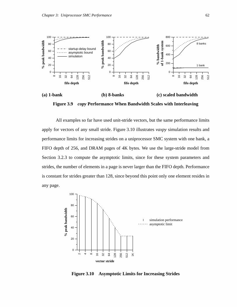
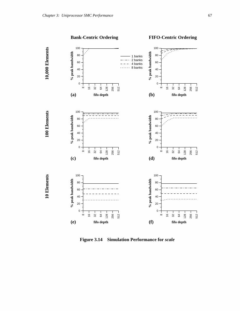
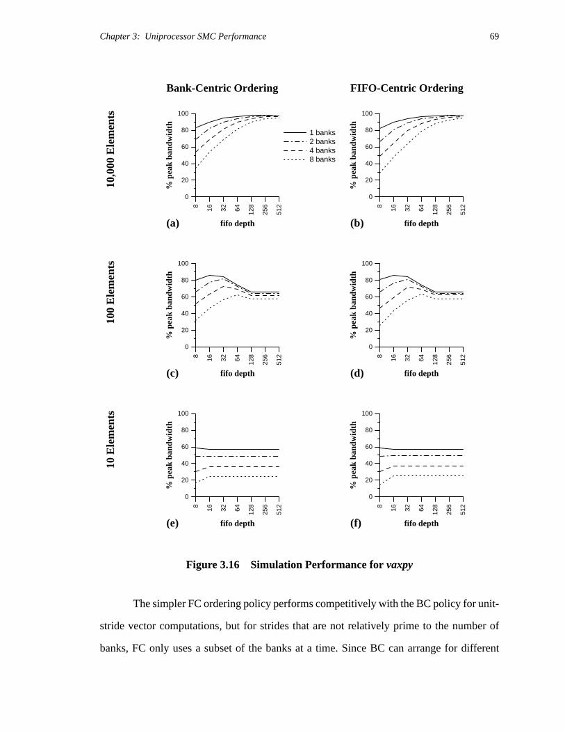
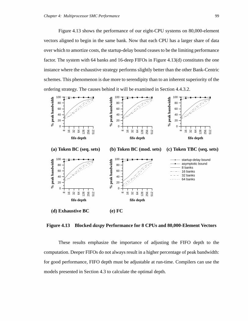
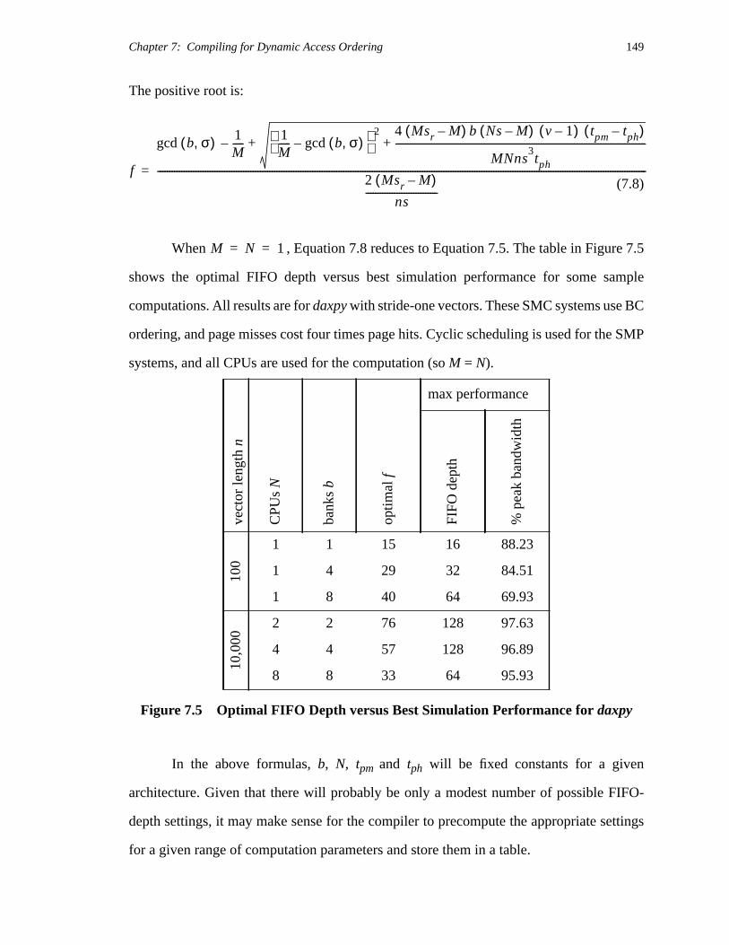
Figure 2.16 presents vector-load performance for vectors of various strides. The

analytic results for streaming were generated using a version of Equation 2.3 that accounts

for the overlapping of cache writes with non-caching reads. In all cases, measured

performance approaches theoretical bounds for large block sizes. Differences for smaller

blocks can be attributed to overhead costs for subroutines and loops, and to page misses

from crossing DRAM page boundaries (our models do not account for such misses).

The performance of stream and sao is fairly independent of vector stride, whereas

the average cost per access of naive ordering rises steadily with increasing stride (up to the

cache line size). For these machine parameters, static access ordering always beats naive

ordering for blocks larger than the cache-line size. The point at which streaming yields

better memory performance than naive caching depends on stride and implementation

details. If the code to perform streaming were generated by the compiler, or if function in-

lining were used to mitigate the costs of a streaming subroutine call, the technique might

become profitable for even smaller block sizes.

2.4 Related Work

In addition to the various access-ordering schemes discussed in the taxonomy of Section

2.2, a large body of research characterizes and evaluates the memory performance of

scientific codes. Most of this research focuses on:

a) hiding or tolerating memory latency,

b) decreasing the number of cache misses incurred, or

c) avoiding bank conflicts in an interleaved memory system.

Nonblocking caches and prefetching to cache [Bae91,Cal91,Dah94, Gup91,Kla91,

Mow92,Soh91], prefetching to registers (as in the IBM 3033 [Kog81], or as proposed by

Fu, Patel, and Janssens [FuP92]), or prefetching to special preload buffers [FuP91] can be

Chapter 2: Access Ordering 39

used to overlap memory accesses with computation, or to overlap the latencies of more than

one access. These methods can improve processor performance, but techniques that simply

mask latency do nothing to increase effective bandwidth. Such techniques are still useful,

but they will be most effective when combined with complementary technology to exploit

memory component capabilities.

Modifying the computation to increase the reuse of cached data can improve

performance dramatically [Gal87,Gan87,Car89,Por89,Wol89,Lam91,Tem93]. These

studies assume a uniform memory access cost, and so they don’t address minimizing the

time to load vector data into cache. These techniques will also deliver better performance

when integrated with methods to make more efficient use of memory resources.

Lam, Rothberg, and Wolf [Lam91] develop a model of data conflicts and

demonstrate that the amount of cache interference is highly dependent on block size and

vector stride, with large variations in performance for matrices of different sizes. For best

results, block size for a computation must be tailored to matrix size and cache parameters,

and efficient blocked access patterns tend to use only a small portion of the cache. This may

limit the applicability of cache-based access ordering techniques discussed here. Block-

size limitations can be circumvented by providing a separate buffer space for vector

operands.

Loshin and Budge [Los92] describe streaming in an article on compiler

management of the memory hierarchy. Lee’s investigations of the NASPACK library and

the work of Meadows, Nakamoto, and Schuster [Mea92] on the PGI i860 compiler both

address streaming in conjunction with other operations. These reports do not attempt to

develop a general performance model, nor do they present measured timing results specific

to this particular optimization.

Chapter 2: Access Ordering 40

Copying incurs an overhead cost proportional to the amount of data being copied,

but the benefits often outweigh the cost [Lam91], and Temam, Granston, and Jalby [Tem93]

present a compile-time technique for determining when copying is advantageous. Using

caching loads to create the copy can cause subtle problems with self-interference. As new

data from the original vector is loaded, it may evict cache lines holding previously copied

data. Explicitly managing the cache becomes easier when a cache bypass mechanism is

available. Data coherence issues must be addressed when vectors are shared (see Section

7.6 and Section 8.1 for a discussion of coherence issues).

Research on blocking and copying has focused primarily on improving

performance for data that is reused, the traditional assumption being that there is no

advantage to applying these transformations to data that is only used once. In contrast,

reports on the NASPACK routines [Lee91,Lee93] and the PGI compiler [Mea92] suggest

that by exploiting memory properties, these techniques may also benefit single-use vectors

and those that do not remain in cache between uses. Our results support these conclusions.

Palacharla and Kessler [Pal95] investigate software restructuring to improve

memory performance on a Cray T3D. This machine includes a single, stride-one “read-

ahead” stream buffer to prefetch data to cache. When enabled, the read-ahead buffer fetches

the next consecutive cache line whenever there is a cache miss. The prefetched data is held

in the buffer until requested by the processor, or until another cache miss occurs, causing

the current read-ahead line to be discarded and another to be prefetched. Exploiting the

read-ahead mechanism also exploits the fast-page mode of the T3D’s memory components.

In order to make effective use of both architectural features, the authors recommend

unrolling loops and grouping accesses to each vector, as in Moyer’s static access ordering

[Moy93]. They also implement block prefetching (as described in Section 2.3.1.2) by

reading one element of each cache line for a block of data before entering the inner loop.

Their measurements indicate that the combination of these schemes yields performance

Chapter 2: Access Ordering 41

improvements from 31% to 75% for simple streaming examples, and overall execution

time improvements from 9% and 30% for the benchmarks they consider. They determine

blocksize dynamically at run-time in order to minimize cache conflicts, but do not

investigate copying to explicitly manage the cache.

Several schemes for avoiding bank contention, either by address transformations,

skewing, prime memory systems, or dynamically scheduling accesses have been published

[Bir91,Bud71,Gao93,Har87,Har89,Rau91]; these, too, are complementary to the

techniques for improving bandwidth that we analyze here.

Both Moyer [Moy91] and Lee [Lee90] investigate the floating point and memory

performance of the i860XR. Results from our experiments with this architecture agree

largely with their findings.

2.5 Summary

As processors become faster, memory bandwidth is rapidly becoming the performance

bottleneck in the application of high performance microprocessors to vector-like

algorithms. Here we have examined the time to load a vector using five different access-

ordering schemes, putting maximum stress on the memory system in order to determine

performance bounds. Four of these schemes are purely software techniques; one requires

the addition of a modest amount of supporting hardware. The more efficient schemes

exploit the ability to bypass the cache.

A comprehensive, successful solution to the memory bandwidth problem must

exploit the richness of the full memory hierarchy: it cannot be treated as though it were

uniform access-time RAM. This requires not only finding ways to improve cache

performance, but providing alternatives for computations that don’t exhibit the properties

necessary to make caching effective.

Chapter 2: Access Ordering 42

This knowledge should guide processor design and operating system

implementation. To get good memory performance, the user needs more control over what

gets cached and how, and mechanisms to take advantage of memory component

capabilities should be readily available. Unfortunately, this is not the case for most current

microprocessor systems. For cases where such mechanisms are available, we have

demonstrated how several straightforward techniques can improve bandwidth

dramatically. These schemes require no heroic compiler technology, and are

complementary to other common code optimizations. Our results indicate that access

ordering can deliver nearly the full memory system bandwidth for streamed computations.

43

Chapter 3

Uniprocessor SMC Performance

The previous chapter demonstrated the impact of access ordering on effective memory

bandwidth when loading a single vector. Of the five approaches studied, dynamic access

ordering boasts the highest upper bound on attainable bandwidth. Given the promise of this

approach, this chapter examines dynamic access ordering in greater detail, analyzing its

performance for dense matrix computations on uniprocessor systems. Later chapters will

consider sparse matrix computations and symmetric multiprocessor systems.

We begin by surveying the design space of access ordering policies for Stream

Memory Controller (SMC) systems. We have developed a set of ordering heuristics for

which we conducted numerous simulation experiments. In order to evaluate the

effectiveness of these heuristics, we extend the analytic model of Chapter 2, Section

2.3.1.5, to describe multiple-stream computations, and we develop a startup-delay model

of the overhead costs incurred by dynamic access ordering. Even though our discussion is

couched in terms of the SMC model, these bounds relate to any scheme that performs

batched ordering by fetching stream or vector data in blocks. Finally, we compare our

I bring fresh showers for the thirsting flowers,From the seas and the streams.

— Percy Bysshe Shelley (1792-1822)

Chapter 3: Uniprocessor SMC Performance 44

analytic bounds to the best performances of any of the simulated ordering heuristics, and

present sample simulation results for two representative ordering policies. The structure of

this chapter is depicted in Figure 3.1:

3.1 Ordering Policy Design Space

By exploiting the underlying memory architecture, dynamic access ordering attempts to

issue accesses in an order that improves memory bandwidth. For any memory system

composed of interleaved banks of DRAM components, there are at least two facets to this

endeavor: taking advantage of the available concurrency among the interleaved banks, and

taking advantage of the device characteristics. At each “decision point” (each available

memory bus cycle), the ordering hardware must decide how best to achieve these goals.

In the following discussion, we assume the FIFO-based SMC implementation

introduced in Chapter 2 and depicted in Figure 3.2. For this organization, the ordering-

policy design space can be divided into two subspaces: algorithms that first choose a bank

(Bank-Centric schemes), and those that first choose a FIFO (FIFO-Centric schemes).1

1. This division of the design space generalizes to implementations that don’t employ FIFOs. Theanalog of a FIFO-Centric scheme would first choose a buffer or a particular vector access.

Figure 3.1 Chapter Structure

Ordering Policy

Bank FIFO

Analytic

ModelingAssumptions

Startup Delay

AsymptoticModels

Uniprocessor SMC Performance

SummaryDesign Space

Selection Selection

Models

Model

SimulationModels

SimulationEnvironment

ComparativeResults

Chapter 3: Uniprocessor SMC Performance 45

In a Bank-Centric (BC) scheme, each bank operates independently; the range of

addresses for one bank’s current DRAM page need not be related to those of another bank’s

current page. Any BC algorithm for choosing the next access must:

1) select the memory bank(s) to which the next access(es) will be issued, and

2) choose an appropriate access from the pool of ready accesses for each memory

bank (this is equivalent to selecting a FIFO to service).

Here a ready access refers to an empty position in a read FIFO (that position is ready to be

filled with the appropriate data element) or a full position in a write FIFO (the

corresponding data element is ready to be written to memory).

FIFO-Centric (FC) schemes perform the two tasks in the reverse order: once the

FIFO to service has been determined, the selection mechanism chooses an appropriate bank

from the set servicing that FIFO.

3.1.1 Bank Selection

BC ordering mechanisms first choose the bank to access. Strategies for selecting banks vary

in the number of banks to which accesses may be issued at once, the number of banks

mem

mem

mem

mem

Mem

ory

Sche

dulin

g U

nit

Stream

CACHE

FIFO

FIFO

FIFO

CPU BufferUnit

Figure 3.2 Uniprocessor Stream Memory Controller (SMC) System

Chapter 3: Uniprocessor SMC Performance 46

considered in the search process, and the order in which they are considered. Let a represent

the number of memory operations that may be initiated during one cycle (for uniprocessors,

in most cases ). The spectrum of bank-selection strategies ranges from an exhaustive

search that keeps looking until a idle banks are found (or no unexamined banks remain) to

the simple strategy that only considers a banks, initiating accesses for the subset of idle

banks. Most of our BC ordering policies start with the next bank in sequence after the one

to which the last access was initiated.

Our BC policies each rely on one of three bank-selection schemes: a parallel

strategy that attempts to initiate accesses to all idle banks at once (this scheme assumes a

separate bus to each bank); a limited (“token-passing”) round-robin strategy that only

considers the next bank in sequence; and a greedy, round-robin strategy that considers each

bank in turn until it finds an idle one for which there exists a ready access.

The first of these attempts to take full advantage of available concurrency, but the

need for multiple buses makes it generally impractical to implement. On the surface, it

seems that this algorithm should perform at least as well as the others, but this isn’t

necessarily so. The interaction between bank availability, access initiation, and processor

activity is complex, and often non-intuitive. The second scheme is the easiest to implement,

and in spite of its simplicity, its performance rivals that of the others. The last scheme

strikes a middle ground in terms of hardware requirements.

3.1.2 Fifo Selection

The spectrum of FIFO-selection schemes ranges from sophisticated algorithms that use all

available information to decide what to do next, to those that make the easiest and quickest

possible choice. For instance, an ordering algorithm may look for an access that hits a

current DRAM page, or it may simply choose the next access from the current FIFO (or the

next FIFO in sequence). If an algorithm looks for a page hit but can’t find one, it may try

a 1=

Chapter 3: Uniprocessor SMC Performance 47

to choose the “best” candidate based on which FIFO requires the most service. When trying

to select the best FIFO, an algorithm may consider the total contents of the FIFO, or it may

restrict itself to just the portion of the FIFO for which a particular bank is responsible (this

is a subFIFO).

Some algorithms require that a FIFO (subFIFO) meet a certain “threshold” in order

to be considered for service; for instance, a read FIFO (subFIFO) might need to be at least

half empty before it can be considered among the best candidates. The rationale for this

springs from the overhead involved in accessing a new DRAM page: any time the SMC

must switch DRAM pages, the cost of that miss should be amortized over as many accesses

as possible. If a FIFO contains sufficiently few ready accesses to a given page, it may be

worthwhile to wait until there are more. If there are no “best” candidates, an algorithm may

either choose the next access in sequence or do nothing until the next decision-making time.

In selecting the “best” FIFO or bank to use next, any access ordering scheme must

impose an ordering on the resources (banks or FIFOs). This priority dictates the order in

which the resources will be considered or which subset will be selected. For instance, our

BC ordering strategies use one of two FIFO orderings: one set of strategies begins its search

by examining the FIFO last accessed by any bank, and the other begins with the FIFO last

accessed by the currently selected bank. The first of these encourages several banks to be

working on the same FIFO, while the second encourages different banks to be working on

different FIFOs. It is not intuitively obvious which of these is preferable, and in fact, our

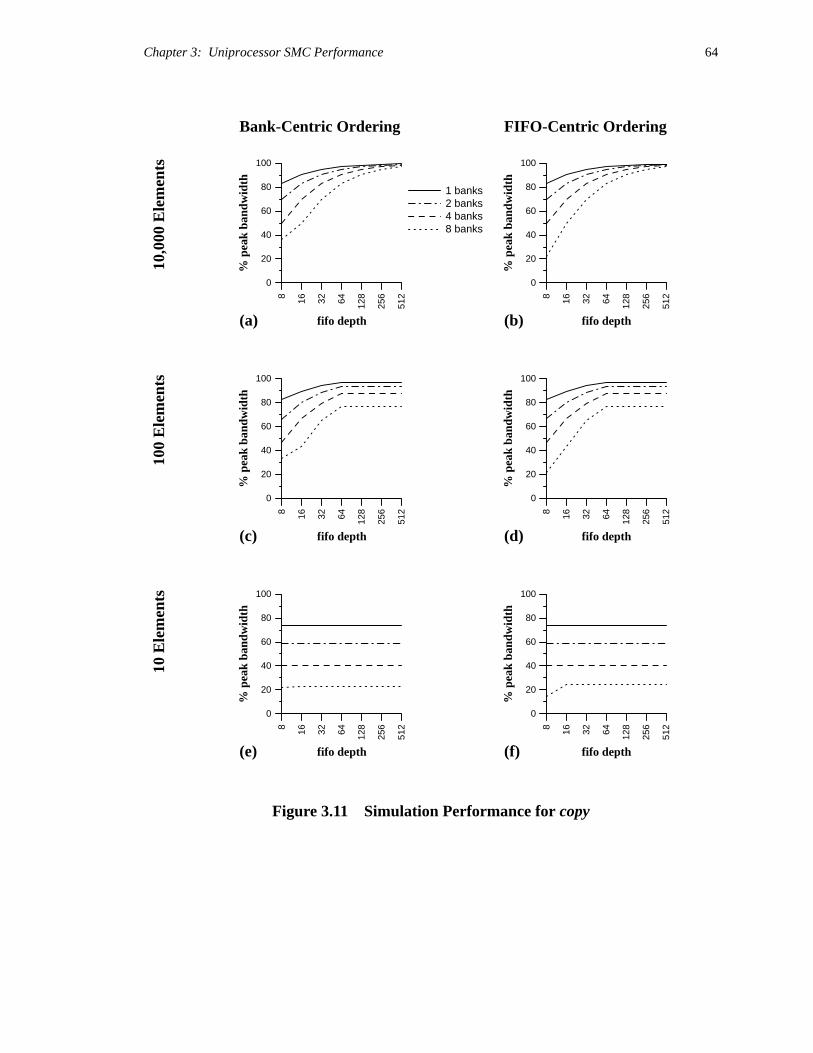
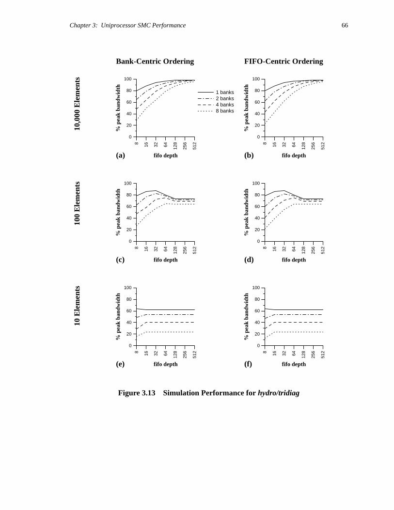
experiments demonstrate no consistent performance advantage to either [McK93a].

3.2 Analytic Models

For the systems we consider, bandwidth is limited by how many page-misses a computation

incurs. This means that we can derive a bound for any ordering algorithm by calculating

the minimum possible number of page-misses, and we can use this bound to evaluate the

Chapter 3: Uniprocessor SMC Performance 48

performance of our heuristics. Similarly, we can calculate the minimum time for a

processor to execute a loop by adding the minimum time the processor must wait to receive

all the operands for the first iteration to the time required to execute all remaining

instructions.

These calculations provide us with two different bounds: the first gives asymptotic

performance limits for very long vectors, and the second describes limits due to startup

effects. The asymptotic model bounds bandwidth between the SMC and memory, whereas

the startup-delay model bounds bandwidth between the processor and SMC.

We first look at how SMC startup costs impact overall performance, then we

examine the limits of the SMC’s ability to amortize page-miss costs as vector length

increases asymptotically. We develop each of these models for uniprocessor SMC systems,

then extend them in Chapter 4 to describe multiprocessor SMC performance.

3.2.1 Modeling Assumptions

We assume the system is matched so that bandwith between the processor and SMC equals

the bandwidth between the SMC and memory, and the vectors we consider are of equal

length and stride, share no DRAM pages in common, and are aligned to begin in the same

bank. We assume a model of operation in which the processor accesses its FIFOs in round-

robin order, consuming one data item from each FIFO during each loop iteration.

In order that the bound we derive be conservative, we impose several constraints.

We ignore bus turnaround delays and other external effects. We model the processor as a

generator of only non-cached loads and stores of vector elements; all other computation is

assumed to be infinitely fast, putting as much stress as possible on the memory system. In

calculating the number of page misses incurred by a multiple-stream computation, we

assume that DRAM pages are infinitely large. Misses resulting from crossing page

boundaries are ignored in our model. Finally, we assume that the SMC always amortizes

Chapter 3: Uniprocessor SMC Performance 49

page miss costs over as many accesses as possible: read FIFOs are completely empty and

write FIFOs are completely full whenever the SMC begins servicing them. Each of these

constraints tends to make the bound more conservative (in the sense that it becomes larger)

and hence harder to achieve in practice.

3.2.2 Startup-Delay Model

Unlike the traditional performance concern over processor utilization, we focus on memory

utilization for stream computations. The processor’s activity affects memory usage, and

thus good overall performance requires that the processor not be left unnecessarily idle:

both resources must be used wisely.

Since we assume the bandwith between the processor and SMC equals that between

the SMC and memory, optimal system performance allows the processor to complete one

memory access each bus cycle. The Memory Scheduling Unit (MSU) attempts to issue as

many accesses as possible to the current DRAM pages, and thus most of our access-

ordering heuristics tend to fill the currently selected FIFO(s) completely before moving on

to service others. At the beginning of a computation on s streams, the processor will stall

waiting for the first element of the sth stream while the MSU fills the FIFOs for the first

streams. By the time the MSU has provided all the operands for the first loop

iteration, it will also have prefetched enough data for many future iterations, and the

computation can proceed without stalling the processor again soon.

Deeper FIFOs cause the processor to wait longer at startup, but if the vectors in the

computation are sufficiently long, these delays are amortized over enough fast accesses to

make them insignificant. Unfortunately, short vectors afford fewer accesses over which to

amortize startup costs; initial delays can represent a significant portion of the computation

time.

s 1–

Chapter 3: Uniprocessor SMC Performance 50

To illustrate the problem, consider an SMC with FIFOs of depth f. If we disregard

DRAM page misses, the total time for a computation is the time to fetch the first iteration’s

operands plus the time to finish processing all data. For a computation involving two read

streams of length , the processor must wait f cycles (while the first FIFO is being

filled) between reading the first operand of the first stream and the first operand of the

second stream. According to our model (in which arithmetic and control are assumed to be

infinitely fast), the actual processing of the data requires cycles, one to read each

element in each vector. For this particular system and computation, this time is at least

cycles. This is only 66% of the optimal performance of cycles (the

minimum time to process all the stream elements). Figure 3.3 presents a time line of this

example: the processor and memory both require the same number of cycles to do their

work, but the extent to which their activities overlap determines the time to completion.

In our analysis, a vector that is only read (or only written) consists of a single

stream, whereas a vector that is read, modified, and rewritten constitutes two streams: a

read-stream and a write-stream. Let and represent the number of read-streams and

write-streams, respectively, and let be the total number of streams in a

computation. The bandwidth limits caused by startup delays can then be described by:

(3.1)

Figure 3.4 illustrates these limits as a function of the log of the ratio of FIFO depth

to vector length for a uniprocessor SMC system reading two streams and writing one. When

n f=

2f

f 2f+ 3f= 2f

0 f 2f 3f

time in cycles

memory busy

processor busy

Figure 3.3 Startup Delay for 2 Read-Streams of Length f

delay

sr sw

s sr sw+=

% peak bandwidthns

f sr 1–( ) ns+---------------------------------- 100.0×=

Chapter 3: Uniprocessor SMC Performance 51

vector length equals the FIFO depth ( ), this particular computation can

exploit at most 75% of the system bandwidth. In contrast, when the vector length is at least

16 times the FIFO depth ( ), startup delays become insignificant, and

attainable bandwidth reaches at least 98% of peak.

3.2.3 Asymptotic Models

If a computation’s vectors are long enough to make startup costs negligible, the limiting

factor becomes the number of fast accesses the SMC can make. The following models

calculate the minimum number of DRAM page misses that a computation must incur.

The terms stream and FIFO will be used interchangeably since each stream is assigned to

one FIFO. For simplicity of presentation we refer to read FIFOs unless otherwise stated;

the analysis for write FIFOs is analogous. We first present a model of small-stride, multiple-

vector computations; we then extend this for single-vector or large-stride computations.

3.2.3.1 Multiple-Vector Computations

Let be the number of interleaved memory banks, and let be the depth of the FIFOs.

Every time the MSU switches FIFOs, it incurs a page miss in each memory bank: the

percentage of accesses that cause DRAM page misses is at least for a stream whose

stride is relatively prime to the number of banks. Strides not relatively prime to the number

of banks prevent us from exploiting the full system bandwidth, since they don’t hit all

f n⁄( ) 0=log

f n⁄( ) 4–=log

Figure 3.4 Performance Limits Due to Startup Delays

-9 -8 -7 -6 -5 -4 -3 -2 -1 0 1 2 3

log(fifo depth/vector length)

0

20

40

60

80

100

max

% p

eak

band

wid

th

b f

b f⁄

Chapter 3: Uniprocessor SMC Performance 52

banks. In calculating performance for vectors with these strides, we must adjust our

formulas to reflect the percentage of banks actually used. We calculate this as the total

number of banks in the system divided by the greatest common denominator of that total

and the vector stride: . The fraction of accesses that miss the page is at least

.

Let be the number of distinct vectors in the computation, and let be the number

of streams ( will be greater than if some vectors are both read and written). If the

processor accesses the FIFOs (in round robin order) at the same rate as the memory system,

then while the MSU is filling a FIFO of depth , the processor will consume more data

elements from that stream, freeing space in the FIFO. While the MSU supplies more

elements, the processor can remove , and so on. Thus the equation for calculating the

miss rate for each vector is:

(3.2)

In the limit, the series in the denominator converges to , and the formula reduces

to .

The number of page misses for each vector is the same, but a read-modify-write

vector is accessed twice as many times as a read-vector and requires two FIFOs, one for the

read-stream and one for the write-stream. For such vectors, the percentage of accesses that

cause page misses is half that of a read-vector. To calculate the average DRAM page-miss

rate for the entire computation, we amortize the per-vector miss rate over all streams. If we

assume that none of the banks is on the correct page when the MSU changes FIFOs, then

this average is . But if:

1) the MSU takes turns servicing each FIFO, providing as much service as possible

before moving on to service another FIFO;

b gcd b σ,( )⁄b gcd b σ,( )⁄

f--------------------------------

v s

s v

f f s⁄

f s⁄

f s2⁄

b gcd b σ,( )⁄

f 1 1s---

1s---

2 1s---

3…+ + + +

-----------------------------------------------------------------------

s s 1–( )⁄b s 1–( )

gcd b σ,( ) f× s------------------------------------

b s 1–( )gcd b σ,( ) f× s------------------------------------ v

s--×

Chapter 3: Uniprocessor SMC Performance 53

2) the MSU has filled all the FIFOs and must wait for the processor to drain them

before issuing more accesses; and

3) the MSU begins servicing the same FIFO it had been working on last,

then the MSU need not pay the DRAM page-miss overhead again at the beginning of the

next turn. The MSU may avoid paying the per-bank page-miss overhead for one vector at

each turn. When we exploit this phenomenon, our average page-miss rate, r, for the whole

computation becomes:

(3.3)

Let tph be the cost of servicing an access that hits the current DRAM page, and let

tpm be the cost of servicing an access that misses the page. Vector strides that are not

relatively prime to the number of banks do not hit all banks, and the maximum achievable

bandwidth for a computation is limited by the percentage of banks used. We must scale our

bandwidth formula accordingly, dividing by the greatest common denominator of the total

number of banks and the vector stride. The asymptotic bound on percentage of peak

bandwidth for the computation is thus:

(3.4)

3.2.3.2 Single-Vector and Large-Stride Computations

For a computation involving a single vector, only the first access to each bank generates a

page miss. If we maintain our assumption that pages are infinitely large, all remaining

accesses will hit the current page. In this case, the model produces a page-miss rate of 0,

and the predicted percentage of peak bandwidth is 100. We can more accurately bound

performance by considering the actual number of data elements in a page and calculating

the precise number of page-misses that the computation will incur.

rb s 1–( )

gcd b σ,( ) f× s------------------------------------ v 1–( )

s------------------× b s 1–( ) v 1–( )

gcd b σ,( ) f× s2

----------------------------------------= =

% peak bandwidth =tph

r tpm×( ) 1 r–( ) tph×( )+------------------------------------------------------------------- 100.0

gcd b σ,( )-------------------------×

Chapter 3: Uniprocessor SMC Performance 54

Likewise, for computations involving vectors with large strides, the predominant

factor affecting performance is no longer FIFO depth, but how many vector elements reside

in a page. The number of elements is the page size divided by the stride of the vector data

within the memory bank, and the distance between elements in a given bank is the vector

stride divided by the number of banks the vector hits. We refer to the latter value as the

effective intrabank stride: . For example, on a system with two interleaved

banks, elements of a stride-2 vector have an effective intrabank stride of 1, and are

contiguous within a single bank of memory.

Decreasing DRAM page size and increasing vector stride affect SMC performance

in similar ways. Let zp be the size of a DRAM page in vector elements. Then for

computations involving either a single vector or multiple vectors with large effective

intrabank strides, the average page-miss rate per FIFO is:

(3.5)

For single-vector computations or computations in which the number of elements

in a page is less than the FIFO depth, we must use Equation 3.5 to compute r. The

percentage of peak bandwidth is then calculated from Equation 3.4, as before. Neither

FIFO depth nor the processor’s access pattern affects performance limits for large-stride

computations.

3.3 Simulation Models

In order to validate the SMC concept, we have simulated a wide range of SMC

configurations and benchmarks, varying dynamic order/issue policy; number of memory

banks; DRAM speed and page size; benchmark kernel; FIFO depth; and vector length,

stride, and alignment with respect to memory banks. The cross product of these parameters

spans a large design space:

σgcd b σ,( )-------------------------

gcd b σ,( ) zp×------------------------------------=

Chapter 3: Uniprocessor SMC Performance 55

The sheer magnitude of this quantity of data and the overwhelming similarity of the

performance curves for most ordering policies argue against including all the results here.

Instead, we present highlights, focusing on general performance trends. Detailed

uniprocessor results can be found in our technical reports [McK93a,McK93c].

3.3.1 Simulation Environment

As mentioned above, we model the processor as a generator of non-cached loads and stores

of vector elements in order to put as much stress as possible on the memory system.

Instruction and scalar data references are assumed to hit in cache, and all stream references

use non-caching loads and stores. All memories modeled here consist of interleaved banks

of page-mode DRAMs, where each page is 4K bytes, and unless otherwise noted, the

DRAM page-miss cycle time is four times that of a page-hit.

The vectors we consider are 10, 100, and 10,000 doublewords in length, and are

aligned to share no DRAM pages. Unless otherwise noted, all vectors begin in the same

bank. We have chosen 10,000 elements as our “long” vectors, although much longer

vectors (on the order of millions of elements) certainly exist in practice. These vectors are

long enough that SMC startup transients become insignificant; performance for million-

element vectors is not materially different. This length is also short enough to represent an

amount of work that can reasonably be accomplished between context switches.

All results are given as a percentage of the system’s peak bandwidth, the bandwidth

necessary to allow the processor to perform a memory operation each cycle. When

correlating the performance bounds of our analytic model with our functional simulation

results, we present only the maximum percentage of peak bandwidth attained by any order/

32orderingpolicies

4memory

configurations

6benchmark

kernels

7FIFOdepths

3vectorlengths

2data

alignments

×× × × × ≈ 32,000data

points

Chapter 3: Uniprocessor SMC Performance 56

issue policy simulated for a given memory system and benchmark. Finally, SMC

initialization requires two writes to memory-mapped registers for each stream; since this

small overhead does not significantly affect our results, it is not included in these results.

3.3.1.1 Benchmark Suite

The benchmark kernels used are listed in Figure 3.5. Daxpy, copy, scale, and swap are from

the BLAS (Basic Linear Algebra Subroutines) [Law79,Don79]. These vector computations

occur frequently in practice, and thus have been collected into libraries of highly optimized

routines for various host architectures. Hydro and tridiag are the first and fifth Livermore

Loops [McM86], a set of kernels culled from important scientific computations. The former

is a fragment of a hydrodynamics computation, and the latter performs tridiagonal gaussian

elimination. Since these two benchmarks share the same access pattern, their simulation

results are identical, and will be presented together. Vaxpy denotes a “vector axpy”

operation: a vector a times a vector x plus a vector y. This computation occurs in matrix-

vector multiplication by diagonals, which is useful for the diagonally sparse matrices that

arise frequently when solving parabolic or elliptic partial differential equations by finite

element or finite difference methods [Gol93].

These benchmarks were selected because they are representative of the access

patterns found in real codes, including the inner loops of blocked algorithms.1 Nonetheless,

our results indicate that variations in the processor’s reference sequence have little effect

on the SMC’s ability to improve bandwidth.

1. For a discussion of blocking, see Chapter 2, Section 2.3.1.2.

Chapter 3: Uniprocessor SMC Performance 57

3.3.1.2 Ordering Policies

The results presented in this chapter focus on two ordering schemes, one Bank-Centric and

one FIFO-Centric. At each available bus cycle, the BC policy considers the next memory

bank, banki. The Memory Scheduling Unit (MSU) tries to issue an access that hits the

current DRAM page, but if no such access exists, it issues an access for the FIFO requiring

the most service from banki. If banki is busy or there are no ready accesses to it, then no

access is initiated during that bus cycle.

In the FC scheme, the MSU services each FIFO in turn, initiating accesses for the

current FIFO until no ready accesses remain. The MSU then advances to the next FIFO and

proceeds to initiate accesses for it. While servicing a particular FIFO, if the next ready

access is to a busy bank, the MSU simply waits until the bank is idle.

3.3.2 Comparative Results

3.3.2.1 Analysis versus Simulation

Figure 3.6 depicts bandwidth as a function of FIFO depth for four of our multiple-vector

benchmarks using 100-element vectors on two different SMC systems. The graphs in the

left column illustrate medium-vector performance on a system with a single bank of

memory; those on the right show performance for a system with eight banks. Figure 3.7

Figure 3.5 Benchmark Algorithms

copy:

daxpy:

hydro:

scale:

swap:

tridiag:

vaxpy:

i∀ yi xi←

i∀ yi axi yi+←

i∀ xi q yi r zxi 10+× t zxi 11+×+( )×+←

i∀ xi axi←

i∀ tmp yi← yi xi← xi tmp←

i∀ xi zi yi xi 1––( )×←

i∀ yi aixi yi+←

Chapter 3: Uniprocessor SMC Performance 58

presents the corresponding data for computations on 10,000-element vectors, and

Figure 3.8 illustrates performance for scale, our single-vector kernel, on the same systems.

For multiple-vector computations on short vectors, the startup-delay bound is the

limiting performance factor, as evidenced by the curves in Figure 3.6. Short vectors prevent

the SMC from effectively amortizing both the startup costs and DRAM page-miss

overheads. Since the computation only uses a portion of each FIFO equal to the vector

length, performance is constant for FIFO depths greater than the vector length. For longer

vectors, as in Figure 3.7, startup-delays cease to impose significant limits to achievable

bandwidth, and simulation performance approaches the asymptotic bound.

SMC performance on the scale benchmark, depicted in Figure 3.8, is consistently

high. With only one vector in the computation, the only page-misses occur at startup and

page boundaries. The longer vectors of Figure 3.8(c) and (d) let the SMC amortize costs

over more accesses. Accordingly, performance for these is up to 20% of peak greater than

for the vectors of Figure 3.8(a) and (b). In both cases, the theoretical limits are nearly 100%.

Chapter 3: Uniprocessor SMC Performance 59

8 16 32 64 128

256

512

fifo depth

0

20

40

60

80

100

% p

eak

band

wid

th

8 16 32 64 128

256

512

fifo depth

0

20

40

60

80

100

% p

eak

band

wid

th

startup-delay boundasymptotic boundsimulation

Figure 3.6 Medium-Vector Performance for Multi-Vector Kernels

8 16 32 64 128

256

512

fifo depth

0

20

40

60

80

100

% p

eak

band

wid

th

8 16 32 64 128

256

512

fifo depth

0

20

40

60

80

100

% p

eak

band

wid

th

8 16 32 64 128

256

512

fifo depth

0

20

40

60

80

100

% p

eak

band

wid

th

8 16 32 64 128

256

512

fifo depth

0

20

40

60

80

100

% p

eak

band

wid

th

(a) (b)

(c) (d)

(e) (f)

8 16 32 64 128

256

512

fifo depth

0

20

40

60

80

100

% p

eak

band

wid

th

8 16 32 64 128

256

512

fifo depth

0

20

40

60

80

100

% p

eak

band

wid

th

(g) (h)

1 Bank 8 Banks

daxp

yhy

dro/

trid

iag

vaxp

ysw

ap

Chapter 3: Uniprocessor SMC Performance 60

8 16 32 64 128

256

512

fifo depth

0

20

40

60

80

100

% p

eak

band

wid

th

8 16 32 64 128

256

512

fifo depth

0

20

40

60

80

100

% p

eak

band

wid

th

startup-delay boundasymptotic boundsimulation

Figure 3.7 Long-Vector Performance for Multi-Vector Kernels

8 16 32 64 128

256

512

fifo depth

0

20

40

60

80

100

% p

eak

band

wid

th

8 16 32 64 128

256

512

fifo depth

0

20

40

60

80

100

% p

eak

band

wid

th

8 16 32 64 128

256

512

fifo depth

0

20

40

60

80

100

% p

eak

band

wid

th

8 16 32 64 128

256

512

fifo depth

0

20

40

60

80

100

% p

eak

band

wid

th

(a) (b)

(c) (d)

(e) (f)

8 16 32 64 128

256

512

fifo depth

0

20

40

60

80

100

% p

eak

band

wid

th

8 16 32 64 128

256

512

fifo depth

0

20

40

60

80

100

% p

eak

band

wid

th

(g) (h)

1 Bank 8 Banks

daxp

yhy

dro/

trid

iag

vaxp

ysw

ap

Chapter 3: Uniprocessor SMC Performance 61

If we increase the number of memory banks, we decrease the number of vector

elements in each bank, which limits the SMC’s ability to amortize page-miss and startup

costs. Performance for systems with fewer banks is thus closer to the asymptotic limits than

for a system with many banks. If we assume that total system bandwidth scales with

interleaving, the latter systems deliver a smaller percentage of a much larger bandwidth.

To illustrate this, Figure 3.9(a) and Figure 3.9(b) show copy performance for long vectors

relative to the peak bandwidth of a 1-bank and an 8-bank system, and Figure 3.9(c)

illustrates how these absolute bandwidths relate to each other.

startup-delay boundasymptotic boundsimulation

Figure 3.8 Long- and Medium-Vector Performance for scale8 16 32 64 128

256

512

fifo depth

0

20

40

60

80

100

% p

eak

band

wid

th

8 16 32 64 128

256

512

fifo depth

0

20

40

60

80

100

% p

eak

band

wid

th

8 16 32 64 128

256

512

fifo depth

0

20

40

60

80

100

% p

eak

band

wid

th

8 16 32 64 128

256

512

fifo depth

0

20

40

60

80

100

% p

eak

band

wid

th

(a) (b)

(c) (d)

1 Bank 8 Banks

10,0

00 E

lem

ents

100

Ele

men

ts

Chapter 3: Uniprocessor SMC Performance 62

All examples so far have used unit-stride vectors, but the same performance limits

apply for vectors of any small stride. Figure 3.10 illustrates vaxpy simulation results and

performance limits for increasing strides on a uniprocessor SMC system with one bank, a

FIFO depth of 256, and DRAM pages of 4K bytes. We use the large-stride model from

Section 3.2.3 to compute the asymptotic limits, since for these system parameters and

strides, the number of elements in a page is never larger than the FIFO depth. Performance

is constant for strides greater than 128, since beyond this point only one element resides in

any page.

8 16 32 64 128

256

512

fifo depth

0

20

40

60

80

100

% p

eak

band

wid

th

8 16 32 64 128

256

512

fifo depth

0

20

40

60

80

100

% p

eak

band

wid

th

8 16 32 64 128

256

512

fifo depth

0

200

400

600

800

% b

andw

idth

of 1

-ban

k sy

stem

1 bank

8 banks

startup-delay boundasymptotic boundsimulation

Figure 3.9 copy Performance When Bandwidth Scales with Interleaving

(a) 1-bank (b) 8-banks (c) scaled bandwidth

2 4 8 16 32 64 128

256

512

1K

vector stride

0

20

40

60

80

100

% p

eak

band

wid

th

simulation performanceasymptotic limit

Figure 3.10 Asymptotic Limits for Increasing Strides

Chapter 3: Uniprocessor SMC Performance 63

3.3.2.2 Bank-Centric versus FIFO-Centric Ordering

Figure 3.11 through Figure 3.16 demonstrate how our two representative ordering

strategies compare for stride-1 vectors on SMC systems with one, two, four, and eight

banks of memory. The similarity in the shapes of the performance curves for the different

benchmarks illustrates the SMC’s relative insensitivity to access patterns in its ability to

improve bandwidth. In all cases, asymptotic behavior for long vectors approaches 100% of

the peak bandwidth that the memory system can deliver. For these vectors, the BC and FC

ordering schemes perform almost identically, the only significant differences occurring for

extremely shallow FIFOs.

Chapter 3: Uniprocessor SMC Performance 64

8 16 32 64 128

256

512

fifo depth

0

20

40

60

80

100

% p

eak

band

wid

th

8 16 32 64 128

256

512

fifo depth

0

20

40

60

80

100

% p

eak

band

wid

th

8 16 32 64 128

256

512

fifo depth

0

20

40

60

80

100

% p

eak

band

wid

th

8 16 32 64 128

256

512

fifo depth

0

20

40

60

80

100

% p

eak

band

wid

th

8 16 32 64 128

256

512

fifo depth

0

20

40

60

80

100

% p

eak

band

wid

th

8 16 32 64 128

256

512

fifo depth

0

20

40

60

80

100

% p

eak

band

wid

th

10,0

00 E

lem

ents

100

Ele

men

ts10

Ele

men

ts

(a) (b)

(c) (d)

(e) (f)

Bank-Centric Ordering FIFO-Centric Ordering

1 banks2 banks4 banks8 banks

Figure 3.11 Simulation Performance for copy

Chapter 3: Uniprocessor SMC Performance 65

8 16 32 64 128

256

512

fifo depth

0

20

40

60

80

100

% p

eak

band

wid

th

8 16 32 64 128

256

512

fifo depth

0

20

40

60

80

100

% p

eak

band

wid

th

8 16 32 64 128

256

512

fifo depth

0

20

40

60

80

100

% p

eak

band

wid

th

8 16 32 64 128

256

512

fifo depth

0

20

40

60

80

100

% p

eak

band

wid

th

8 16 32 64 128

256

512

fifo depth

0

20

40

60

80

100

% p

eak

band

wid

th

8 16 32 64 128

256

512

fifo depth

0

20

40

60

80

100

% p

eak

band

wid

th

10,0

00 E

lem

ents

100

Ele

men

ts10

Ele

men

ts

(a) (b)

(c) (d)

(e) (f)

Bank-Centric Ordering FIFO-Centric Ordering

1 banks2 banks4 banks8 banks

Figure 3.12 Simulation Performance for daxpy

Chapter 3: Uniprocessor SMC Performance 66

8 16 32 64 128

256

512

fifo depth

0

20

40

60

80

100

% p

eak

band

wid

th

8 16 32 64 128

256

512

fifo depth

0

20

40

60

80

100

% p

eak

band

wid

th

8 16 32 64 128

256

512

fifo depth

0

20

40

60

80

100

% p

eak

band

wid

th

8 16 32 64 128

256

512

fifo depth

0

20

40

60

80

100

% p

eak

band

wid

th

8 16 32 64 128

256

512

fifo depth

0

20

40

60

80

100

% p

eak

band

wid

th

8 16 32 64 128

256

512

fifo depth

0

20

40

60

80

100

% p

eak

band

wid

th

10,0

00 E

lem

ents

100

Ele

men

ts10

Ele

men

ts

(a) (b)

(c) (d)

(e) (f)

Bank-Centric Ordering FIFO-Centric Ordering

1 banks2 banks4 banks8 banks

Figure 3.13 Simulation Performance for hydro/tridiag

Chapter 3: Uniprocessor SMC Performance 67

8 16 32 64 128

256

512

fifo depth

0

20

40

60

80

100

% p

eak

band

wid

th

8 16 32 64 128

256

512

fifo depth

0

20

40

60

80

100

% p

eak

band

wid

th

8 16 32 64 128

256

512

fifo depth

0

20

40

60

80

100

% p

eak

band

wid

th

8 16 32 64 128

256

512

fifo depth

0

20

40

60

80

100

% p

eak

band

wid

th

8 16 32 64 128

256

512

fifo depth

0

20

40

60

80

100

% p

eak

band

wid

th

8 16 32 64 128

256

512

fifo depth

0

20

40

60

80

100

% p

eak

band

wid

th

10,0

00 E

lem

ents

100

Ele

men

ts10

Ele

men

ts

(a) (b)

(c) (d)

(e) (f)

Bank-Centric Ordering FIFO-Centric Ordering

1 banks2 banks4 banks8 banks

Figure 3.14 Simulation Performance for scale

Chapter 3: Uniprocessor SMC Performance 68

8 16 32 64 128

256

512

fifo depth

0

20

40

60

80

100

% p

eak

band

wid

th

8 16 32 64 128

256

512

fifo depth

0

20

40

60

80

100

% p

eak

band

wid

th

8 16 32 64 128

256

512

fifo depth

0

20

40

60

80

100

% p

eak

band

wid

th

8 16 32 64 128

256

512

fifo depth

0

20

40

60

80

100

% p

eak

band

wid

th

8 16 32 64 128

256

512

fifo depth

0

20

40

60

80

100

% p

eak

band

wid

th

8 16 32 64 128

256

512

fifo depth

0

20

40

60

80

100

% p

eak

band

wid

th

10,0

00 E

lem

ents

100

Ele

men

ts10

Ele

men

ts

(a) (b)

(c) (d)

(e) (f)

Bank-Centric Ordering FIFO-Centric Ordering

1 banks2 banks4 banks8 banks

Figure 3.15 Simulation Performance for swap

Chapter 3: Uniprocessor SMC Performance 69

The simpler FC ordering policy performs competitively with the BC policy for unit-

stride vector computations, but for strides that are not relatively prime to the number of

banks, FC only uses a subset of the banks at a time. Since BC can arrange for different

8 16 32 64 128

256

512

fifo depth

0

20

40

60

80

100

% p

eak

band

wid

th

8 16 32 64 128

256

512

fifo depth

0

20

40

60

80

100

% p

eak

band

wid

th

8 16 32 64 128

256

512

fifo depth

0

20

40

60

80

100

% p

eak

band

wid

th

8 16 32 64 128

256

512

fifo depth

0

20

40

60

80

100

% p

eak

band

wid

th

8 16 32 64 128

256

512

fifo depth

0

20

40

60

80

100

% p

eak

band

wid

th

8 16 32 64 128

256

512

fifo depth

0

20

40

60

80

100

% p

eak

band

wid

th

10,0

00 E

lem

ents

100

Ele

men

ts10

Ele

men

ts

(a) (b)

(c) (d)

(e) (f)

Bank-Centric Ordering FIFO-Centric Ordering

1 banks2 banks4 banks8 banks

Figure 3.16 Simulation Performance for vaxpy

Chapter 3: Uniprocessor SMC Performance 70

subsets of banks to be servicing different FIFOs simultaneously, it can exploit the

concurrency of the memory system under a greater variety of circumstances. Even the most

sophisticated ordering cannot compensate for an unfortunate data placement, though — for

instance, if all operands were to reside in a single bank of an interleaved system. To

illustrate the differences between the BC and FC ordering policies, Figure 3.17 depicts a

snapshot of SMC activity for each scheme on a computation involving two stride-2 vectors

that reside in different banks. Here we show what happens when the base address of vector

x hits bank0 and the base address of vector y hits bank1. The BC scheme of Figure 3.17(a)

keeps all banks busy, but because the FC scheme of Figure 3.17(b) only fills one FIFO at a

time, it can only use half the banks.

Figure 3.18 demonstrates the differences in performance between BC and FC

ordering for non-unit stride, long-vector computations on a system with eight banks. As in

our previous examples, the vectors in Figure 3.18(a) and (b) are aligned such that the ith

elements of all vectors reside in the same bank. For Figure 3.18(c) and (d), we staggered

the vectors so that the ith vector of each kernel begins in banki.

x[0]

x[1]

x[0]

x[1]

idle

idley[0]

y[1]

FIFO 0

FIFO 1

FIFO 0

FIFO 1

(a) Bank-Centric Ordering (b) FIFO-Centric Ordering

SBU Banks SBU Banks

Figure 3.17 Bank Concurrency for Stride-2 Vectors with Staggered Alignment

Chapter 3: Uniprocessor SMC Performance 71

For non-unit stride vectors, the first alignment causes the computation to use only a

subset of the banks, restricting achievable bandwidth on the 8-bank system to 50%, 25%,

and 12.5% of peak for strides of 2, 4, and 8, respectively. The computations represented in

Figure 3.18(d) are subject to the same limits: since the FC scheme only services one stream

at a time, relative alignment of the vectors has no effect on performance. In contrast, the

BC scheme is able to overlap accesses to different banks, exploiting more of the memory

system’s concurrency. Bandwidth for vectors of stride 2, 4, and 8 reach 66%, 50%, and 25%

of peak, respectively, as illustrated in Figure 3.18(c). This represents a performance

improvement of 32% for stride-2 vectors, and 100% for larger strides.

Figure 3.18 BC versus FC for Non-Unit Stride vaxpy

8 16 32 64 128

256

512

fifo depth

0

20

40

60

80

100

% p

eak

band

wid

th

8 16 32 64 128

256

512

fifo depth

0

20

40

60

80

100

% p

eak

band

wid

th

8 16 32 64 128

256

512

fifo depth

0

20

40

60

80

100

% p

eak

band

wid

th

8 16 32 64 128

256

512

fifo depth

0

20

40

60

80

100

% p

eak

band

wid

th

(a) (b)

(c) (d)

alig

ned

vect

ors

stag

gere

d ve

ctor

s

Bank-Centric Ordering FIFO-Centric Ordering

stride 1stride 2stride 4stride 8

Chapter 3: Uniprocessor SMC Performance 72

3.3.2.3 Reordered versus Natural-Order Accesses

Graphs (e) and (f) in Figure 3.11 through Figure 3.16 illustrate SMC performance on very

short vectors, only 10 elements in length. For these computations, bandwidth is entirely

dominated by the startup-delay bound. Although performance is not as dramatic as for very

long vectors, the SMC is still able to deliver between 55% and 75% of peak bandwidth for

all benchmarks on a single-bank system. This represents a significant performance

improvement over using non-caching loads and stores in the natural order for these

computations. Figure 3.19 depicts the relationships between non-SMC and SMC

performance for all benchmarks and vector lengths on systems with one and eight memory

banks.1 Because the accesses take the same amount of time for each iteration, the

percentage of bandwidth exploited in the natural-order computations is independent of

vector length.

Figure 3.19(a) and (b) represent performance when all vectors begin in the same

bank. Figure 3.19(c) uses the staggered alignment, as per Figure 3.18(c). Staggering the

vectors tends to reduce the number of bank conflicts for the natural-order computations,

and so the percentages of peak bandwidth for the non-SMC case tend to be slightly higher

in Figure 3.18(c) than in Figure 3.18(b). Because the SMC reorders accesses, differences

in operand alignment have little effect on its ability to maximize bandwidth: the SMC

performances in Figure 3.19(b) and (c) are almost identical.

1. The non-SMC data was generated with Moyer’s static access ordering software [Moy93].

Chapter 3: Uniprocessor SMC Performance 73

3.4 Summary

In Chapter 2 we saw that reordering can optimize stream accesses to exploit the underlying

memory architecture. In this chapter, we investigated combining compile-time detection of

streams with execution-time selection of the access order and issue. We described the basic

nonS

MC

10 S

MC

100

SM

C10

,000

SM

C

nonS

MC

10 S

MC

100

SM

C10

,000

SM

C

nonS

MC

10 S

MC

100

SM

C10

,000

SM

C

nonS

MC

10 S

MC

100

SM

C10

,000

SM

C

nonS

MC

10 S

MC

100

SM

C10

,000

SM

C

nonS

MC

10 S

MC

100

SM

C10

,000

SM

C

0

20

40

60

80

100

max

% p

eak

band

wid

th

copy daxpy hydro scale swap vaxpy

nonS

MC

10 S

MC

100

SM

C10

,000

SM

C

nonS

MC

10 S

MC

100

SM

C10

,000

SM

C

nonS

MC

10 S

MC

100

SM

C10

,000

SM

C

nonS

MC

10 S

MC

100

SM

C10

,000

SM

C

nonS

MC

10 S

MC

100

SM

C10

,000

SM

C

nonS

MC

10 S

MC

100

SM

C10

,000

SM

C

0

20

40

60

80

100

max

% p

eak

band

wid

th

copy daxpy hydro scale swap vaxpy

Figure 3.19 Comparison of Non-SMC and SMC Performance

1 ba

nk8

bank

s, a

ligne

d ve

ctor

s

(a)

(b)

nonS

MC

10 S

MC

100

SM

C10

,000

SM

C

nonS

MC

10 S

MC

100

SM

C10

,000

SM

C

nonS

MC

10 S

MC

100

SM

C10

,000

SM

C

nonS

MC

10 S

MC

100

SM

C10

,000

SM

C

nonS

MC

10 S

MC

100

SM

C10

,000

SM

C

nonS

MC

10 S

MC

100

SM

C10

,000

SM

C

0

20

40

60

80

100

max

% p

eak

band

wid

th

copy daxpy hydro scale swap vaxpy

8 ba

nks,

sta

gger

ed v

ecto

rs

(c)

Chapter 3: Uniprocessor SMC Performance 74

design of a uniprocessor Stream Memory Controller (SMC), developed analytic models to

bound its performance, and analyzed its simulation performance for a wide variety of

design parameter values. Two different limits govern the percentage of peak bandwidth

delivered:

- startup-delay bounds, or the amount of time a processor must wait to receive data

for the first iteration of an inner loop; and

- asymptotic bounds, or the number of fast accesses over which the SMC can

amortize DRAM page-miss costs.

Our analysis and simulation indicate that, using current memory parts and only a few

hundred words of buffer storage, an SMC system can consistently achieve nearly the peak

bandwidth that the memory system can deliver. Moreover, it does so with naive code, and

performance is independent of operand alignment.

In addition, our results emphasize an important consideration in the design of an

efficient SMC system that was initially a surprise to us — FIFO depth must be selectable

at run-time so that the amount of stream buffer space to use can be adapted to individual

computations. Using the equations presented here, compilers can either compute optimal

FIFO depth (if the vector lengths are known), or they can generate code to perform the

calculation at run-time.

75

Chapter 4

Multiprocessor SMC Performance

The previous chapter demonstrated that dynamic access ordering can significantly improve

bandwidth for dense matrix computations on uniprocessor systems. This chapter explores

the usefulness of the technique for the same class of computations on modest-size

symmetric multiprocessor (SMP) systems.

Figure 4.1 Chapter Structure

System

Analytic

Startup Delay AsymptoticModels

Symmetric Multiprocessor SMC Performance

ConclusionsArchitecture

Bounds

Model

SimulationModels

Performance

TaskScheduling

FactorsOrderingPolicies

Results

Related Work

Chapter 4: Multiprocessor SMC Performance 76

4.1 System Architecture

When adapting the general SMC framework to an SMP system, a number of options

exist regarding component placement. The most efficient organization is one in which the

entire SMC system and all processors reside on a single chip; this is the organization we

consider here. Since we assume a modest number of processors, such an implementation

should soon be possible. If a single-chip implementation is not feasible, however, several

options remain. Placing a full SMC system on each chip is likely to scale poorly and be

prohibitively expensive, since extensive inter-MSU communication would be needed to

coordinate accesses to the shared memory system. In contrast, a single, centralized,

external SMC should perform well for a moderate number of processors. A third, hybrid

approach places the SBUs on-chip while the centralized access-order/issue logic remains

external. The MSU would need to consider the costs of moving data on and off the

processor/SBU chips, but amortizing such costs is precisely what the MSU does well; such

an organization should therefore perform competitively with the single-chip version, but

verifying this assertion is beyond the scope of this dissertation.

In the multiprocessor SMC system in Figure 4.2, all processors are interfaced to

memory through a centralized Memory Scheduling Unit. The architecture is similar to that

of the uniprocessor SMC, but here each CPU has its own Stream Buffer Unit. Note that

MSU

SBU

CACHECPU

mem

mem

mem

mem

SBU

CACHECPU

Figure 4.2 Symmetric Multiprocessor SMC Organization

Chapter 4: Multiprocessor SMC Performance 77

since cache placement does not affect the SMC, logically the system could consist of a

single cache for all CPUs or separate caches for each — the choice is an implementation

issue. Figure 4.2 depicts separate caches to emphasize that the SBUs and cache reside at

the same logical level of the memory hierarchy.

Due to both the high communication requirements for a fully distributed approach

and the limitations on the number of processors that may share a centralized resource, we

do not expect SMP SMC systems to scale to large numbers of processors. Here we focus

on the performance of SMP systems with two to eight processors. Analysis of SMC

systems that scale to larger numbers of CPUs an interesting issue for further research.

4.2 Task Partitioning

The way in which a computation is partitioned for a multiprocessor can have a marked

effect on bandwidth. In particular, SMC performance is influenced by whether the working

sets of DRAM pages needed by different processors overlap during the course of the

computation. If they overlap, the set of FIFOs using data from a page will be larger. With

more buffer space devoted to operands from that page, more accesses can be issued to it in

succession, resulting in greater bandwidth. Three general scheduling techniques are

commonly used to parallelize workloads: prescheduling, static scheduling, and dynamic

scheduling [Ost89].1

Prescheduling requires that the programmer divide the workload among the

processors before compiling the program. There is no notion of dynamic load balancing

with respect to data size or number of processors. This type of scheduling is particularly

appropriate for applications exhibiting functional parallelism, where each CPU performs a

different task. Since performance on a single CPU is relatively independent of access

pattern [McK93a], we model prescheduled computations by running the same benchmark

1. As in Osterhaug [Ost89], we use scheduling to refer to when and how a computation is dividedinto tasks. For the purposes of this discussion, scheduling is synonymous with partitioning.

Chapter 4: Multiprocessor SMC Performance 78

on all processors. The vector is split into approximately equal-size pieces, and each

processor performs the computation on a single piece. Figure 4.3 depicts this data

distribution for a stride-1 vector, and the corresponding inner loops for a two-CPU system.

In static scheduling, tasks are divided among the processors at runtime, but the

partitioning is performed in some predetermined way. Thus a process must determine

which tasks it must do, perform that work, then wait for other processes to finish their tasks.

We model static scheduling by distributing loop iterations among the processors, as in a

Fortran DOALL loop. This parallelization scheme, also known as cyclic scheduling, makes

the effective stride at each of the participating CPUs , where represents the

natural stride of the computation. Depending on the number of memory banks relative to

the number of processors and the strides and alignment of the vectors, a different subset of

banks may provide all data for each processor. Figure 4.4 illustrates the data distribution

and code for this scheme. Since each of the CPUs performs every th iteration, all

processors use the same set of DRAM pages throughout most of the computation. If the

CPUs proceed at different rates, some may cross page boundaries slightly sooner than

others, but recent empirical studies suggest that the slowest processor is normally not more

than the mean execution time of one loop iteration behind the average processor [LiN94].

Alternatively, a static scheduling scheme could partition the data as we have done

for prescheduling. SMC results for this kind of block scheduling would be identical to those

for our model of prescheduling. We will use the term “block scheduling” when referring to

the performance of both prescheduling and static block scheduling.

Figure 4.3 Prescheduling: Data Distribution for 2-CPU System

CPU0 CPU1

for (i = 0; i < n/2; i++) {/* operations on x[i]*/

}

for (i = n/2; i < n; i++) {/* operations on x[i]*/

}

vector x:

CPU0’s code:

CPU1’s code:

address α address (α + n × 8 bytes)

M M σ× σ

M M

Chapter 4: Multiprocessor SMC Performance 79

In dynamic scheduling, a pool of tasks is maintained. Each processor schedules its

own tasks by repeatedly removing a task from the pool and performing it; if the pool is

empty, the CPUs wait for tasks to appear. For a computation’s inner loops, SMC

performance for dynamic scheduling is similar to either block scheduling or cyclic

scheduling, depending on how the work is apportioned into tasks. We therefore omit

separate results for this scheduling technique.

4.3 Analytic Bounds

As in the uniprocessor models of Chapter 3, we derive bounds on both the maximum

possible bandwidth (via calculating the minimum number of page-misses) and the

minimum execution time for a computation on a given multiprocessor SMC system. We

then use these bounds to evaluate the performance of our ordering heuristics. Our

assumptions are those of Section 3.2.1:

- the system is matched so that bandwith between the processor and SMC equals

the bandwidth between the SMC and memory;

- the processor generates only non-cached loads and stores of vector elements;

- vectors are of equal length and stride, share no DRAM pages in common, and are

aligned to begin in the same bank;

- each processor accesses its FIFOs in round-robin order, consuming one data item

from each FIFO during each loop iteration;

CPU0

CPU1CPU0

CPU1CPU0

CPU1

…vector x:

Figure 4.4 Cyclic Static Scheduling: Data Distribution for a 2-CPU System

address α address (α + n × 8 bytes) for (i = 0; i < n; i += 2) {/* operations on x[i]*/

}

for (i = 1; i < n; i += 2) {/* operations on x[i]*/

}

CPU0’s code:

CPU1’s code:

Chapter 4: Multiprocessor SMC Performance 80

- bus turnaround delays are ignored;

- DRAM pages are infinitely large (that is, page misses from crossing DRAM page

boundaries are ignored); and

- read FIFOs are completely empty and write FIFOs completely full whenever the

SMC begins servicing them.

In addition, we assume that each vector is divided into equal-size blocks, with each

CPU responsible for processing one block.

4.3.1 Startup-Delay Model

In a multiprocessor environment, we can bound the performance of the entire parallel

computation by first calculating the minimum delay for the last CPU to begin its share of

the processing, and then adding the minimum time for that CPU to execute its remaining

iterations. In developing these formulas, we assume that all CPUs are performing the same

operation, but are acting on different data.

Here, as before, is the depth of the FIFOs, is the vector length, and and

represent the total number of streams and the number of read-streams in a computation,

respectively. N is the number of processors in the system, and M is the number of those that

participate in the computation. Note that in our multiprocessor formulas, reflects the

length of the entire vector being processed in parallel, thus we use to indicate the

amount of data being processed by a single CPU. The startup-delay formula for

uniprocessor SMC systems, developed in Section 3.2.2, is:

(4.1)

We will derive two models, each tailored to a particular SMC implementation. The

way in which the MSU fills the FIFOs affects how long the CPUs must wait to receive the

operands for their first iteration. If the MSU’s ordering heuristic only services one FIFO at

f n s sr

n

n M⁄

% peak bandwidth 100nsf sr 1–( ) ns+----------------------------------=

Chapter 4: Multiprocessor SMC Performance 81

a time, then the last CPU must wait while the MSU fetches the read-streams for all other

processors plus all but one of its own read-streams. On the other hand, if the MSU can

service more than one FIFO at a time, all CPUs can start computing sooner.

In the former case, when the MSU only services one FIFO at a time, the minimum

number of cycles required to fill that FIFO is times the minimum for a uniprocessor

system (because the bandwidth of the system is balanced, and there are now CPUs that

can each execute a memory reference per cycle). Let represent the number of processors

participating in the computation. Then the CPUs are using times the potential

bandwidth, and the number of streams that must be fetched before the last CPU can start is

. Each of these streams is of length . The startup-delay formula under

these circumstances is:

(4.2)

For the latter case, let us assume that the MSU can perform accesses to FIFOs

at a time (one FIFO for each participating CPU). Each processor need only wait for all but

one of its own read-streams to be fetched, and the average rate at which those FIFOs are

filled will be one element per processor cycle. When , the formula for startup

delays is the same as for the uniprocessor SMC system (Equation 4.1) for vectors of length

. When , the average time to fill a FIFO will be times that for a

uniprocessor, and the general formula becomes:

(4.3)

1 N⁄

N

M

M N⁄

M sr×( ) 1– n M⁄

%peak bandwidths

1N----

fn M⁄------------

Msr 1–( ) s+----------------------------------------------------------------- M

N----- 100××=

100MnsMf Msr 1–( ) Nns+-------------------------------------------------=

M

M N=

n M⁄ M N< M N⁄

% peak bandwidths

MN-----

fn M⁄------------

sr 1–( ) s+------------------------------------------------------------ M

N----- 100××=

100MnsMf Msr M–( ) Nns+---------------------------------------------------=

Chapter 4: Multiprocessor SMC Performance 82

The startup delays for the two cases differ only by a factor of in the first term

of the sum in the denominator. Equation 4.2 bounds bandwidth for block-scheduled

workloads (where different CPUs share no DRAM pages) and for MSUs that use FIFO-

Centric ordering (described in Section 3.1). Equation 4.3 bounds bandwidth for cyclically

scheduled workloads and MSUs that use Bank-Centric ordering. Of course, Equation 4.3

can be used for the same situations as Equation 4.2, but it computes a looser bound.

4.3.2 Asymptotic Models

In Section 3.2.3 we developed models to calculate the minimum number of DRAM page

misses that a computation must incur on a uniprocessor SMC system. This lets us derive

the theoretical maximum bandwidth for a particular computation and system. Here we

extend those models to bound SMC performance on symmetric multiprocessor systems.

Given the similarity of the memory subsystems for the SMC organizations

described in Figure 3.2 and Figure 4.2, we might expect an SMP SMC system to behave

much like a uniprocessor SMC with a large number of FIFOs. For SMP systems, though,

some of the assumptions made in the uniprocessor performance models no longer hold. For

instance, we can no longer assume that each stream occupies only one FIFO. As we saw in

Section 4.2, the distribution of vectors among the FIFOs depends upon how the workload

is parallelized. The parallelization scheme affects the processors’ pattern of DRAM page-

sharing, which in turn affects performance.

In the following, tph and tpm represent the cost of servicing DRAM page-hits and

page-misses, respectively; and are the number of streams and vectors in the

computation, and indicates the stride, or distance between their consecutive elements;

denotes the number of interleaved memory banks, and indicates how many

of those are hit by the vector stride; denotes the FIFO depth; and finally, denotes the

page-miss rate for the computation.

M 1–

s v

σ b

b gcd b σ,( )⁄

f r

Chapter 4: Multiprocessor SMC Performance 83

In Chapter 3, we developed bandwidth limits for uniprocessor SMC computations:

(4.4)

The global page-miss rate, , for multiple-vector, small stride computations is:

(4.5)

For single-vector or large-stride computations and DRAM pages of zp elements:

(4.6)

In extending these models to multiprocessor systems, we can bound SMC

performance for both block-scheduled and cyclically scheduled workloads by calculating

the minimum number of page misses for the extreme case when all CPUs share the same

DRAM pages. We could also compute a very conservative estimate of performance by

calculating the maximum percentage of peak bandwidth that is achievable when no CPUs

share DRAM pages at any point in the computation.

The system is balanced so that if each of CPUs can consume a data item each

cycle, the memory system provides enough bandwidth to perform fast accesses (page

hits) in each processor cycle. Each processor can only consume data from its set of FIFOs,

while the MSU may arrange for all accesses to be for a single FIFO at a time: this means

that the memory system can now fill a FIFO times faster. Let be the number of CPUs

participating in the computation. When all processors use the same DRAM pages, we have

distributed each of our streams over FIFOs (each stream is assigned to a single FIFO

per CPU). This situation is analogous to using a single FIFO of depth for each

stream.

% peak bandwidthtph

r tpm×( ) 1 r–( ) tph×( )+------------------------------------------------------------------- 100.0

gcd b σ,( )-------------------------×=

100tph

r tpm tph–( )×( ) gcd b σ,( ) tphgcd b σ,( )+-----------------------------------------------------------------------------------------------------------=

r

rb s 1–( ) v 1–( )

gcd b σ,( ) f× s2

----------------------------------------=

gcd b σ,( ) zp×------------------------------------=

N

N

N M

s M

F M f×=

Chapter 4: Multiprocessor SMC Performance 84

Since we assume a model of computation in which each processor accesses its

FIFOs in round-robin order, consuming one data item from a FIFO at each access, it takes

the MSU cycles to supply items for a stream. During this time, each CPU will

consume more data elements from this stream, for a total of freed FIFO positions.

While the MSU is filling those FIFO positions (in cycles), the CPU can remove

more, and so on. Thus our model for calculating the page-miss rate of each stream becomes:

(4.7)

The series in the denominator converges to , and our equation

for the average page-miss rate is now:

(4.8)

The percentage of peak bandwidth is computed as in Equation 4.4:

4.4 Simulation Models

Having derived the analytic bounds on attainable bandwidth, we now compare them with

the simulation performance of the multiprocessor SMC systems we consider. The

environment and benchmark suite for our SMP simulation models are the same as for a

uniprocessor SMC, and are described in Section 3.3.1. The vectors used here are 10,000

and 80,000 elements in length, and are aligned to share no DRAM pages in common.

Unless otherwise noted, all vectors begin in the same bank.

All results are given as a percentage of the system’s peak bandwidth, the bandwidth

necessary to allow each CPU to perform a memory operation each processor cycle. As in

Chapter 3, when correlating the performance bounds of our analytic model with our

F N⁄ F

FNs------ MF

Ns---------

MF

N2s

--------- M2F

N2s

2-----------

b gcd b σ,( )⁄

F 1 MNs------

MNs------

2 MNs------

3…+ + + +

------------------------------------------------------------------------------------

FNs( ) Ns M–( )⁄

rb gcd b σ,( )⁄

FNs( ) Ns M–( )⁄---------------------------------------------- v 1–

s-----------× b Ns M–( ) v 1–( )

gcd b σ,( ) F× Ns2

----------------------------------------------= =

% peak bandwidth =100tph

r tpm tph–( )×( ) gcd b σ,( ) tphgcd b σ,( )+-----------------------------------------------------------------------------------------------------------

Chapter 4: Multiprocessor SMC Performance 85

functional simulation results, we present only the maximum percentage of peak bandwidth

attained by any order/issue policy simulated for a given memory system and benchmark.

4.4.1 Ordering Policy

The overwhelming similarity of the performance curves presented in Chapter 3 and our

uniprocessor SMC studies indicates that neither the ordering strategy nor the processor’s

access pattern has a large effect on the MSU’s ability to optimize bandwidth [McK93a,

McK93c]. For moderately long vectors whose stride is relatively prime to the number of

memory banks, the SMC consistently delivers nearly the full system bandwidth.

In symmetric multiprocessor SMC systems, however, there are more factors that

can potentially affect performance, thus different partitioning techniques and vector

alignments may benefit from different ordering algorithms. In particular, the task-

scheduling technique may:

- change the effective vector stride on any processor (as in cyclic scheduling), and

- affect the “working set” of DRAM pages that are needed during a portion of the

computation (with cyclic scheduling, all processors are likely to be using the same

set of DRAM pages, whereas with block scheduling, different processors are

likely to be working on different sets of pages).

By exploiting the underlying memory architecture, the SMC attempts to issue

accesses in an order that optimizes bandwidth. Section 3.1 describes the two subspaces of

the design space of access-order/issue algorithms: algorithms that first choose a bank

(Bank-Centric schemes), and algorithms that first choose a FIFO (FIFO-Centric schemes).

In order to select the “best” FIFO or bank to use next, an access ordering scheme

must either consider all possibilities in parallel, or it must impose some ordering on the

resources (FIFOs or banks) so that it can examine them sequentially. Our simulations

Chapter 4: Multiprocessor SMC Performance 86

assume that not all possibilities can be evaluated at once. We therefore model

multiprocessor SMC systems using several resource-ordering variations in order to

determine their effects on performance.

For instance, the order in which the FIFOs are considered for service can affect

delivered bandwidth. We investigate two different ways in which the MSU selects the next

FIFO to service: by examining the FIFOS in sequential round-robin order by processor (all

of CPU0’s FIFOs are considered before any of CPU1’s), and by examining the FIFOs in an

interleaved, round-robin order (in which the MSU first considers FIFO0 for CPU0, then

FIFO0 for CPU1, etc., before considering FIFO1 for CPU0).

4.4.1.1 Bank-Centric Approach

In any Bank-Centric ordering policy, the MSU’s job can be broken into two subtasks:

selecting the banks to use next, and deciding which accesses from which FIFOs to issue to

those banks. We consider two strategies for making the bank selection: Exhaustive Round-

Robin Selection and Token Round-Robin Selection. In the Exhaustive Round-Robin (or just

Exhaustive) selection scheme, the MSU considers each bank in turn until it has initiated as

many accesses as it can, or it has considered all banks. This strategy starts its search by

considering the bank after the last one to which the MSU initiated an access.

With Token Round-Robin selection (Token), the MSU only considers a subset of the

banks at each decision point, attempting to issue accesses to the idle ones. We examine two

different ways of partitioning the banks into subsets. If the MSU can issue up to accesses

at a time, the first algorithm considers the next set of banks in sequence. Thus the first

set contains banks {bank0, …, bankN-1}, the second contains {bankN, …, bank2N-1}, and

so forth. We refer to this ordering as sequential bank sets. In the second variation, a set

contains all banks whose indices are congruent modulo the number of processors: {bank0,

bankN, bank2N, …}, etc. We refer to this as modular bank sets.

N

N

Chapter 4: Multiprocessor SMC Performance 87

Once the MSU has selected a set of banks, it must then decide which accesses to issue. We

examine two related schemes for choosing the FIFO to service, both of which are described

in Chapter 3. We refer to the first FIFO-selection policy as simply the Bank-Centric

algorithm, or BC. For a selected memory bank, banki, the algorithm examines the FIFOs in

order, beginning with the last FIFO for which an access to banki was initiated. If the MSU

finds a ready access that hits banki’s current DRAM page, it issues that access. If no ready

accesses for the bank hit the current DRAM page, then an access is issued for the FIFO

requiring the most service from banki. (This is the BC ordering policy of Section 3.3.1.2.)

The second FIFO-selection algorithm is a more sophisticated variant of the first.

Consider the case where no ready accesses hit the current DRAM page. Instead of initiating

an access for the FIFO requiring the most service from the current bank, the MSU issues

an access only if a FIFO meets the following threshold-of-service criterion. The portion of

a read FIFO for which the current memory bank is responsible must be at least half empty,

or the corresponding portion of a write FIFO must be at least half full. This ensures that

there will be several fast accesses over which to amortize the cost of switching the DRAM

page. We refer to this scheme as the Threshold Bank-Centric algorithm, or TBC.

4.4.1.2 FIFO-Centric Approach

The second class of access-ordering schemes contains those that first choose a FIFO to

service, and then issue accesses from that FIFO to their corresponding banks as appropriate.

We investigate a very simple FIFO-Centric, or FC, algorithm: the SMC looks at each FIFO

in turn, issuing accesses for the same FIFO stream while:

1) not all elements of the stream have been accessed, and

2) there is room in the FIFO for another read operand, or another write operand is

present in the FIFO.

Chapter 4: Multiprocessor SMC Performance 88

If the current FIFO contains no ready accesses to an idle bank, no access is initiated. (This

is the FC ordering policy of Section 3.3.1.2.)

4.4.1.3 Algorithms Simulated

There are many possible means of choosing which banks to access, which FIFOs to service,

and in what order to consider each of these resources in making these decisions. These

elements can be combined in myriad ways. Here we focus on five strategies that generally

perform well and are representative examples from the design space of dynamic ordering

policies:

1) Exhaustive Round-Robin Bank-Centric selection with sequential bank sets,

2) Token Round-Robin Bank-Centric selection with sequential bank sets,

3) Token Round-Robin Bank-Centric selection with modular bank sets,

4) Token Round-Robin Threshold Bank-Centric selection with sequential bank sets,

and

5) FIFO-Centric Selection

We expect Token BC selection to perform about the same as Exhaustive BC

selection, but the former should be less expensive to implement. We investigate two types

of Token BC selection — one using sequential bank sets and one using modular bank sets

— in order to determine what effects the bank-ordering scheme has on performance. We

also look at Token selection with a threshold-of-service requirement (Token TBC) to

determine whether implementing a threshold criterion improves performance, and if so, by

how much. Finally, we compare the performance of the Bank-Centric approaches to that of

our simple, FIFO-Centric (FC) policy. FC is the most economical policy to implement, but

we expect that it will not perform as well as the more sophisticated BC policies for all

system configurations and workloads.

Chapter 4: Multiprocessor SMC Performance 89

The relationships between the elements of these ordering strategies can be

represented as a tree in which the path to each leaf designates a particular policy, as in

Figure 4.5.1

4.4.2 Performance Factors

The percentage of peak bandwidth delivered is ultimately determined by the MSU’s ability

to exploit both fast accesses (in the form of DRAM page hits) and the memory system’s

concurrency. The MSU’s effectiveness can be influenced by several factors, including:

- data distribution

- FIFO depth, and

- workload distribution.

These contribute in varying degrees to SMP SMC performance, thus we first take a

closer look at them in order to better interpret the results presented in Section 4.4.3.

1. In the uniprocessor SMC study, FC is called A1, Token BC is called T1, Token TBC is called T2,and Exhaustive BC is called R1 [McK93a].

Access-Ordering Policies

Bank-Centric FIFO-Centric

Exhaustive Token

sequential modular

Threshold-of-ServiceNo

Bank Selection Bank Selection

Threshold-of-ServiceCriterion Criterion

NoThreshold-of-Service

Criterion

bank sets bank setssequentialbank sets

sequentialbank sets

Figure 4.5 Five Ordering Policies

Chapter 4: Multiprocessor SMC Performance 90

4.4.2.1 Data Layout

As noted in Section 4.2, SMC performance is dramatically affected by whether the working

sets of DRAM pages needed by different processors overlap during the course of the

computation. If they do overlap, the set of FIFOs using data from a page will be larger. With

more buffer space devoted to operands from a page, more (fast) accesses can be issued to

it in succession.

For the experiments described here, we use a DRAM page size of 4K bytes (so each

page holds 512 eight-byte elements). On an eight-way interleaved memory, we incur an

initial page miss on each bank, but the computation does not cross page boundaries until

elements of a given vector have been accessed. On a 16-bank system, the

vectors cross DRAM page boundaries at element 8192; on a 32-bank system, at element

16,384; and so on. Figure 4.6 illustrates the layout of a vector with respect to DRAM pages

for block-scheduled workloads where the page size times the interleaving factor is slightly

less than the amount of data to be processed at each of CPUs.

On a two-CPU system with eight banks, block scheduling divides a 10,000-element

vector so that each CPU processes approximately 5000 elements, thus the streams for the

two CPUs never share pages during the computation. The data layout for each bank is

pictured in Figure 4.7(a). This figure presents much the same information as in Figure 4.6,

except that the vector blocks for each processor have been arranged vertically to indicate

the portions of data that are being processed in parallel by the different CPUs.

512 8× 4096=

M

CPU0 CPU1

DRAM page A DRAM page B DRAM page C

Figure 4.6 Vector Layout in Memory

Chapter 4: Multiprocessor SMC Performance 91

Figure 4.7(b) shows the distribution of the same 10,000-element vector on a four-

CPU system with eight banks; the pattern of DRAM page-sharing between CPU0 and

CPU1 is essentially the same as for a two-CPU, 16-bank system (but in that case each CPU

would process twice as many elements). CPU0 and CPU1 share DRAM pages for almost

two-thirds of the computation, and CPU3 and CPU4 share for the initial one-third. At the

end, CPU2 and CPU3 will be on the same pages.

On a four-CPU system with 16 banks, all processors share the same pages for about

one-third of the computation, with three processors sharing throughout. On a 32-bank, four-

CPU system the computation never crosses a page boundary. This high degree of page-

sharing among processors maximizes the MSU’s ability to issue fast accesses.

When we use block scheduling to parallelize a computation on 80,000-element

vectors, no page-sharing among CPUs is possible for the modest-size SMP systems we

investigate here. For an eight-CPU system, the data is divided so that each CPU processes

10,000 elements. Thus each processor crosses at least two DRAM page boundaries during

its computation. This data layout, pictured in Figure 4.8, causes the MSU to switch DRAM

pages frequently, which decreases effective bandwidth.

CPU0

CPU3

CPU2

CPU1

Figure 4.7 Distribution of 10,000-Element Vector for 8 Banks

(b) 4 CPUs

CPU0

CPU1

(a) 2 CPUs

Chapter 4: Multiprocessor SMC Performance 92

The equations of Section 4.3.2 compute an upper bound on attainable bandwidth for

a computation, but we can compute a better performance estimate if we take into account

the different page-sharing patterns encountered during the course of the block-scheduled

computation, adjusting the number of vectors and streams accordingly. For instance, if we

draw a vertical line at each of the page boundaries in Figure 4.7(b), we divide the

computation into three distinct phases, each having a different page-sharing pattern. If we

then assume that all processors proceed at approximately the same rate — that is, if we

assume that the spatial divisions of data correspond to temporal phases of the computation

— we can apply the asymptotic model to each phase, computing the overall percentage of

peak bandwidth as a weighted average of the maximum performances.

For cyclic task scheduling, each of CPUs performs every th iteration of the loop being

parallelized. Thus all processors access the same set of DRAM pages during any phase of

the computation, resulting in fewer page misses and higher bandwidth.

4.4.2.2 FIFO depth

The second factor affecting SMC performance is FIFO depth. The effect of using deeper

FIFOs is similar to that for increasing DRAM page-sharing among the processors: deeper

FIFOs provide more buffer space devoted to operands from a given page, enabling the

CPU0

CPU3

CPU2

CPU1

CPU4

CPU7

CPU6

CPU5

Figure 4.8 Blocked Distribution of 80,000 Elements for 8 Banks and 8 CPUs

M M

Chapter 4: Multiprocessor SMC Performance 93

MSU to amortize DRAM page-miss overheads over a greater number of fast accesses.

Longer FIFOs result in a larger startup cost, though: if the vectors in the computation are

not sufficiently long in relation to the FIFO depth, the startup costs will not be amortized

effectively, resulting in poorer overall performance.

4.4.2.3 Workload Distribution

Workload distribution is the third factor influencing SMC performance. Data layout and

FIFO depth can interact to create an uneven distribution of the workload over time:

depending on when a processor starts its computation and on the pattern of DRAM page-

sharing among the CPUs, some CPUs may finish before others. For instance, processors

sharing many DRAM pages are likely to finish earlier than others. This happens because

the MSU accesses the shared pages more frequently, attempting to perform as many fast

accesses as it can before performing accesses that generate DRAM page-misses. When a

processor drops out of the computation, the MSU’s pool of potential accesses shrinks.

While the last CPUs are finishing up at the end of the computation, the MSU may not be

able to keep the memory banks busy. As FIFO depth increases, the “faster” processors tend

to finish even earlier, the ending phase becomes longer, and performance suffers even more.

4.4.3 Results

As in Chapter 3, all results are given as a percentage of peak bandwidth, where peak

bandwidth represents the performance attainable if each processor could complete a

memory access every cycle. Performance is presented as a function of FIFO depth and

number of memory banks (available concurrency in the memory system). Unless otherwise

stated, all vectors are aligned to DRAM page boundaries, tasks are apportioned such that

all vectors (and each CPU’s vector blocks, for block-scheduled workloads) are aligned to

begin in bank0, and the MSU uses interleaved FIFO ordering. The multiprocessor SMC

technical report [McK94c] gives complete simulation results for all benchmarks on a wider

range of SMC configurations. We present only highlights of these results here.

Chapter 4: Multiprocessor SMC Performance 94

The number of banks is kept proportional to the number of processors, thus the

curves for an eight-CPU system represent performance on a system with four times the

number of banks as the corresponding curves for a two-CPU system. We keep the peak

memory system bandwidth and DRAM page-miss/page-hit cost ratio constant. This means

that for our experiments, an eight-bank system has four times the DRAM page-miss latency

as a two-bank system. Increasing the number of banks results in fewer total accesses to each

bank. Since page-miss costs are amortized over fewer fast accesses in a system with 16

banks than in a system with two banks, the performance curves for the 16-bank system

represent a smaller portion of a much larger bandwidth.

Building an SMC system with a FIFO depth less than the number of memory banks

would prevent the MSU to exploit the full concurrency of the memory system in most

cases. Nonetheless, we include results for such systems for completeness, for purposes of

comparison, and to illustrate an interesting behavior.

4.4.3.1 Block Scheduling versus Cyclic Scheduling

Block scheduling breaks the vectors into chunks, assigning each chunk to a different CPU

to be processed. Given that the effects of changes in relative vector alignment, vector

length, or the implementation of an ordering policy (e.g. different FIFO orderings) are

fairly independent of the processor’s access pattern, most of the graphs presented here

focus on a single benchmark, daxpy. Like the uniprocessor SMC systems studied

[McK93a], multiprocessor SMC performance approaches (and often exceeds) 90% of the

peak system bandwidth for sufficiently long vectors and appropriately-sized FIFOs.

Figure 4.9 through Figure 4.11 present performance curves for daxpy on 10,000-

element vectors and each of our five ordering schemes on SMP SMC systems with two,

four, and eight processors. Each graph includes the startup-delay performance bound, and

Chapter 4: Multiprocessor SMC Performance 95

the asymptotic bound for a system in which the number of banks equals the number of

processors. Asymptotic bounds for other systems are omitted for the sake of readability.

The overwhelming similarity of the curves within each figure (underscored by the

fact that these results are representative of those for all benchmarks) leads us to conclude

that small variations in the dynamic access-ordering policy have little effect on

performance. For instance, in most cases Token Bank-Centric ordering (TBC), with its

threshold-of-service criterion, performs almost identically to simple Bank-Centric ordering

(BC). When their performances differ, TBC’s is slightly lower. Exhaustive bank-selection

affords little advantage over either variation of the simpler Token bank selection. Similarly,

changing the ordering in which banks or FIFOs are considered generally results in

performance differences of less than 1% of peak [McK94c].

8 16 32 64 128

256

512

fifo depth

0

20

40

60

80

100

% p

eak

band

wid

th

8 16 32 64 128

256

512

fifo depth

0

20

40

60

80

100

% p

eak

band

wid

th

8 16 32 64 128

256

512

fifo depth

0

20

40

60

80

100

% p

eak

band

wid

th

(a) Token BC (seq. sets)8 16 32 64 128

256

512

fifo depth

0

20

40

60

80

100

% p

eak

band

wid

th(b) Token BC (mod. sets)

8 16 32 64 128

256

512

fifo depth

0

20

40

60

80

100

% p

eak

band

wid

th

(c) Token TBC (seq. sets)

(d) Exhaustive BC (e) FC

startup-delay boundasymptotic bound2 banks4 banks8 banks16 banks

Figure 4.9 Blocked daxpy Performance for 2 CPUs

Chapter 4: Multiprocessor SMC Performance 96

FIFO-Centric ordering performs slightly worse than Bank-Centric ordering for

relatively shallow FIFO depths. Because the simpler FC scheme concentrates on servicing

a single FIFO for as long as possible, it cannot take full advantage of DRAM page-sharing

among different FIFOs. Nonetheless, for FIFOs of depth 256 or 512, FC’s performance is

competitive with BC’s. Henceforth when we refer to BC access ordering, we shall mean

BC using the Token selection variation with sequential bank ordering, unless otherwise

stated. This particular scheme is representative of the family of general Bank-Centric

schemes: they all perform similarly. Section 4.6 discusses the tradeoffs in implementing BC

over FC, or vice versa.

8 16 32 64 128

256

512

fifo depth

0

20

40

60

80

100

% p

eak

band

wid

th

8 16 32 64 128

256

512

fifo depth

0

20

40

60

80

100

% p

eak

band

wid

th

8 16 32 64 128

256

512

fifo depth

0

20

40

60

80

100

% p

eak

band

wid

th

(a) Token BC (seq. sets)

8 16 32 64 128

256

512

fifo depth

0

20

40

60

80

100

% p

eak

band

wid

th

(b) Token BC (mod. sets)

8 16 32 64 128

256

512

fifo depth

0

20

40

60

80

100

% p

eak

band

wid

th

(c) Token TBC (seq. sets)

(d) Exhaustive BC (e) FC

startup-delay boundasymptotic bound4 banks8 banks16 banks32 banks

Figure 4.10 Blocked daxpy Performance for 4 CPUs

Chapter 4: Multiprocessor SMC Performance 97

For the simulations represented in Figure 4.9 through Figure 4.11, all vector blocks

were aligned to begin in bank0. To evaluate the performance effects of operand alignment,

we simulated our benchmarks again, this time aligning the vector data for CPUi to begin in

bank on a system with banks and processors. Figure 4.12 illustrates

daxpy performance for BC ordering with both operand alignments. Performance is similar

for both data layouts: the largest differences occur for the four-CPU system with 32 banks

and 8-deep or 32-deep FIFOs, and for the eight-CPU systems with 8N banks and eight-deep

or 16-deep FIFOs. Four four CPUs and FIFOs of depth 8 and 32, the SMC delivers 7.6%

of peak bandwidth less and 6.2% of peak bandwidth more, respectively, when the operands

are aligned to a single bank. For eight CPUs, the differences are as large as 17% of peak.

These effects are due to bank concurrency, and are discussed in Section 4.4.3.2.

8 16 32 64 128

256

512

fifo depth

0

20

40

60

80

100

% p

eak

band

wid

th

8 16 32 64 128

256

512

fifo depth

0

20

40

60

80

100

% p

eak

band

wid

th

8 16 32 64 128

256

512

fifo depth

0

20

40

60

80

100

% p

eak

band

wid

th

(a) Token BC (seq. sets)

8 16 32 64 128

256

512

fifo depth

0

20

40

60

80

100

% p

eak

band

wid

th

(b) Token BC (mod. sets)

8 16 32 64 128

256

512

fifo depth

0

20

40

60

80

100

% p

eak

band

wid

th

(c) Token TBC (seq. sets)

(d) Exhaustive BC (e) FC

startup-delay boundasymptotic bound8 banks16 banks32 banks64 banks

Figure 4.11 Blocked daxpy Performance for 8 CPUs

banki b N⁄( )× b N

Chapter 4: Multiprocessor SMC Performance 98

The curves in Figure 4.9 through Figure 4.12 illustrate the relationship between

FIFO depth and vector length: as the number of processors grows and the amount of data

processed by each CPU decreases, performance becomes limited by the startup-delay

bound. For instance, this bound only begins to dominate performance at FIFO depths 64

and 128 for the two-bank, two-CPU systems in Figure 4.12(a) and (d), but the crossover

point between the startup-delay and the asymptotic bounds is between 32 and 64 for the

eight-CPU systems in Figure 4.12(c) and (f). When an appropriate FIFO depth is used, the

systems with two, four, and eight CPUs and an equivalent number of memory banks all

deliver over 90% of peak bandwidth. Systems with more banks deliver at least 82% of

peak.

8 16 32 64 128

256

512

fifo depth

0

20

40

60

80

100

% p

eak

band

wid

th

2 CPUs

8 16 32 64 128

256

512

fifo depth

0

20

40

60

80

100

% p

eak

band

wid

th

4 CPUs

8 16 32 64 128

256

512

fifo depth

0

20

40

60

80

100

% p

eak

band

wid

th

8 CPUs

startup-delay boundasymptotic boundN banks2N banks4N banks8N banks

Figure 4.12 Blocked daxpy Performance for 2 Data Alignments

8 16 32 64 128

256

512

fifo depth

0

20

40

60

80

100%

pea

k ba

ndw

idth

8 16 32 64 128

256

512

fifo depth

0

20

40

60

80

100

% p

eak

band

wid

th

8 16 32 64 128

256

512

fifo depth

0

20

40

60

80

100

% p

eak

band

wid

th

(a) (b) (c)

(d) (e) (f)

regu

lar

alig

nmen

tst

agge

red

alig

nmen

t

Chapter 4: Multiprocessor SMC Performance 99

Figure 4.13 shows the performance of our eight-CPU systems on 80,000-element

vectors aligned to begin in the same bank. Now that each CPU has a larger share of data

over which to amortize costs, the startup-delay bound ceases to be the limiting performance

factor. The system with 64 banks and 16-deep FIFOs in Figure 4.13(d) constitutes the one

instance where the exhaustive strategy performs slightly better than the other Bank-Centric

schemes. This phenomenon is due more to serendipity than to an inherent superiority of the

ordering strategy. The causes behind it will be examined in Section 4.4.3.2.

These results emphasize the importance of adjusting the FIFO depth to the

computation. Deeper FIFOs do not always result in a higher percentage of peak bandwidth:

for good performance, FIFO depth must be adjustable at run-time. Compilers can use the

models presented in Section 4.3 to calculate the optimal depth.

8 16 32 64 128

256

512

fifo depth

0

20

40

60

80

100

% p

eak

band

wid

th

8 16 32 64 128

256

512

fifo depth

0

20

40

60

80

100

% p

eak

band

wid

th

(a) Token BC (seq. sets)

8 16 32 64 128

256

512

fifo depth

0

20

40

60

80

100

% p

eak

band

wid

th

(b) Token BC (mod. sets)

8 16 32 64 128

256

512

fifo depth

0

20

40

60

80

100

% p

eak

band

wid

th

(c) Token TBC (seq. sets)

(d) Exhaustive BC (e) FC

startup-delay boundasymptotic bound8 banks16 banks32 banks64 banks

Figure 4.13 Blocked daxpy Performance for 8 CPUs and 80,000-Element Vectors

8 16 32 64 128

256

512

fifo depth

0

20

40

60

80

100

% p

eak

band

wid

th

Chapter 4: Multiprocessor SMC Performance 100

Whereas block scheduling parallelizes a task by breaking a vector into chunks and

distributing them among the processors, cyclic scheduling interleaves loop iterations across

the computational elements, thus each of the CPUs participating in a computation would

be responsible for every th iteration. Figure 4.14 through Figure 4.17 illustrate

performance for SMP SMC systems using cyclic scheduling. These systems have two to

eight processors, and all CPUs are used in each computation. Since all processors use the

same DRAM pages throughout the computation, the performance delivered by SMP SMC

systems using this scheduling technique is almost identical to that for the analogous

uniprocessor SMC systems: for long vectors, deep FIFOs, and workloads that allow the

MSU to fully exploit bank concurrency, the SMC can consistently deliver almost the full

system bandwidth.

M

M8 16 32 64 128

256

512

fifo depth

0

20

40

60

80

100

% p

eak

band

wid

th

8 16 32 64 128

256

512

fifo depth

0

20

40

60

80

100

% p

eak

band

wid

th

8 16 32 64 128

256

512

fifo depth

0

20

40

60

80

100

% p

eak

band

wid

th

(a) Token BC (seq. sets)

8 16 32 64 128

256

512

fifo depth

0

20

40

60

80

100

% p

eak

band

wid

th

(b) Token BC (mod. sets)

8 16 32 64 128

256

512

fifo depth

0

20

40

60

80

100

% p

eak

band

wid

th

(c) Token TBC (seq. sets)

(d) Exhaustive BC (e) FC

startup-delay boundasymptotic bound2 banks4 banks8 banks16 banks

Figure 4.14 Cyclic daxpy Performance for 2 CPUs

Chapter 4: Multiprocessor SMC Performance 101

Figure 4.14 illustrates the percentages of peak bandwidth attained for 10,000-

element daxpy on two-CPU systems under the five dynamic access-ordering policies.

Figure 4.15 and Figure 4.16 depict analogous results for SMC systems with four and eight

processors, and Figure 4.17 illustrates performance for eight CPUs and 80,000-element

vectors. Included in each graph are startup-delay bounds and asymptotic performance

bounds for systems in which the number of banks equals the number of processors.

When cyclic scheduling is used, SMP SMC performance is insensitive to variations

in BC ordering, and is almost constant for a given ratio of CPUs to banks. For instance, the

bandwidth attained by the eight-CPU systems with FIFO depths up to 32 differs from that

delivered by the analogous two-CPU systems by less than 1% of peak bandwidth. At FIFO

depths of 256 and 512, these differences are less than 4.1% and 8.9% of peak, respectively.

8 16 32 64 128

256

512

fifo depth

0

20

40

60

80

100

% p

eak

band

wid

th

8 16 32 64 128

256

512

fifo depth

0

20

40

60

80

100

% p

eak

band

wid

th

8 16 32 64 128

256

512

fifo depth

0

20

40

60

80

100

% p

eak

band

wid

th

(a) Token BC (seq. sets)

8 16 32 64 128

256

512

fifo depth

0

20

40

60

80

100

% p

eak

band

wid

th

(b) Token BC (mod. sets)

8 16 32 64 128

256

512

fifo depth

0

20

40

60

80

100

% p

eak

band

wid

th

(c) Token TBC (seq. sets)

(d) Exhaustive BC (e) FC

startup-delay boundasymptotic bound4 banks8 banks16 banks32 banks

Figure 4.15 Cyclic daxpy Performance for 4 CPUs

Chapter 4: Multiprocessor SMC Performance 102

In contrast, as the number of processors increases, attainable bandwidth for the

FIFO-Centric scheme is severely limited by lack of bank concurrency. With cyclic

scheduling, the effective stride for each FIFO becomes the natural stride, , multiplied by

, the number of participating CPUs, since each processor operates only on every th

vector element. The effective stride thus causes each FIFO to use only of the banks

used by the natural stride. This means that when , an SMC system using FC

ordering will probably not be able to exploit the full system bandwidth. When all vectors

are aligned to begin in the same bank, performance for a computation whose natural stride

is relatively prime to the number of banks is generally limited to 50% of peak bandwidth

for the two-CPU systems, 25% for the four-CPU systems, and 12.5% for the eight-CPU

systems. Performance for other natural strides will be even lower.

8 16 32 64 128

256

512

fifo depth

0

20

40

60

80

100

% p

eak

band

wid

th

8 16 32 64 128

256

512

fifo depth

0

20

40

60

80

100

% p

eak

band

wid

th

8 16 32 64 128

256

512

fifo depth

0

20

40

60

80

100

% p

eak

band

wid

th

(a) Token BC (seq. sets)

8 16 32 64 128

256

512

fifo depth

0

20

40

60

80

100

% p

eak

band

wid

th

(b) Token BC (mod. sets)

8 16 32 64 128

256

512

fifo depth

0

20

40

60

80

100

% p

eak

band

wid

th

(c) Token TBC (seq. sets)

(d) Exhaustive BC (e) FC

startup-delay boundasymptotic bound8 banks16 banks32 banks64 banks

Figure 4.16 Cyclic daxpy Performance for 8 CPUs

ς

M M

1 M⁄

M N=

Chapter 4: Multiprocessor SMC Performance 103

Cyclic scheduling may still be used profitably with FC ordering by using only a

subset of the processors, the size of which must be chosen to be relatively prime to the

number of memory banks. This makes the effective stride relatively prime, thereby

maximizing the MSU’s ability to exploit memory system concurrency. Under these

circumstances, attainable bandwidth becomes limited by the percentage of CPUs used,

rather than by the percentage of memory banks used. To see this, consider the graphs in

Figure 4.18. The graphs in the top row show daxpy performance for SMP SMC systems

with FC ordering when all CPUs are used. Those on the bottom indicate performance when

one fewer processors is used. Whether or not using fewer CPUs yields a net performance

gain depends on the total number of processors and the FIFO depth.

8 16 32 64 128

256

512

fifo depth

0

20

40

60

80

100

% p

eak

band

wid

th

8 16 32 64 128

256

512

fifo depth

0

20

40

60

80

100

% p

eak

band

wid

th

8 16 32 64 128

256

512

fifo depth

0

20

40

60

80

100

% p

eak

band

wid

th

(a) Token BC (seq. sets)

8 16 32 64 128

256

512

fifo depth

0

20

40

60

80

100

% p

eak

band

wid

th

(b) Token BC (mod. sets)

8 16 32 64 128

256

512

fifo depth

0

20

40

60

80

100

% p

eak

band

wid

th

(c) Token TBC (seq. sets)

(d) Exhaustive BC (e) FC

startup-delay boundasymptotic bound8 banks16 banks32 banks64 banks

Figure 4.17 Cyclic daxpy Performance for 8 CPUs and 80,000-Element Vectors

Chapter 4: Multiprocessor SMC Performance 104

For instance, in Figure 4.18(a), performance is limited to 50% of peak because the

MSU uses only half the memory banks at a time. This happens because cyclic scheduling

makes the computation’s effective stride times the natural stride; for this example, the

effective stride is 2, and the data for any given FIFO will only hit every other memory bank.

Performance is also limited to 50% of peak in Figure 4.18(d), but for a different reason:

here only one processor is being used. Even though the attainable performance for very

deep FIFOs is the same in both cases, performance for shallower FIFOs is not identical: at

FIFO depths of 32 to 256, the workloads of Figure 4.18(d) achieve a greater percentage of

peak bandwidth.

For FC ordering and cyclically scheduled workloads on systems with four or more

CPUs and adequate FIFO depth, performance improves dramatically when using one fewer

CPUs. For example, when only three of the four CPUs are used, the system with four banks

M

8 16 32 64 128

256

512

fifo depth

0

20

40

60

80

100

% p

eak

band

wid

th

8 16 32 64 128

256

512

fifo depth

0

20

40

60

80

100

% p

eak

band

wid

th

2 CPUs

8 16 32 64 128

256

512

fifo depth

0

20

40

60

80

100

% p

eak

band

wid

th

4 CPUs

8 16 32 64 128

256

512

fifo depth

0

20

40

60

80

100

% p

eak

band

wid

th

8 CPUs

startup-delay boundasymptotic boundN banks2N banks4N banks8N banks

8 16 32 64 128

256

512

fifo depth

0

20

40

60

80

100

% p

eak

band

wid

th

8 16 32 64 128

256

512

fifo depth

0

20

40

60

80

100

% p

eak

band

wid

th(a) (b) (c)

(d) (e) (f)

usin

gM

=N C

PU

sus

ing

M=N

-1 C

PU

s

Figure 4.18 Cyclic daxpy Performance for FC Ordering

Chapter 4: Multiprocessor SMC Performance 105

shown in Figure 4.18(e) delivers 74.6% of peak bandwidth at a FIFO depth of 32, as

compared with 24.3% when all CPUs are used, as in Figure 4.18(b). As the total number of

processors increases, performance differences become even more dramatic. The eight-CPU

system with eight banks in Figure 4.18(f) delivers 83.2% of peak at a depth of 128 when

only seven processors are used. In contrast, the same system using all eight CPUs reaches

only 12.3% of peak, as depicted in Figure 4.18(c).

For very shallow FIFOs, systems with many banks deliver better performance than

those with few. This happens because the FC ordering mechanism forces the MSU of a

many-bank system to switch FIFOs often. The phenomenon is evident in the performance

curves for systems with banks in Figure 4.18, and will be discussed in Section 4.4.3.2.8N

8 16 32 64 128

256

512

fifo depth

0

20

40

60

80

100

% p

eak

band

wid

th

8 16 32 64 128

256

512

fifo depth

0

20

40

60

80

100

% p

eak

band

wid

th

2 CPUs

8 16 32 64 128

256

512

fifo depth

0

20

40

60

80

100

% p

eak

band

wid

th

4 CPUs

8 16 32 64 128

256

512

fifo depth

0

20

40

60

80

100

% p

eak

band

wid

th

8 CPUs

startup-delay boundasymptotic boundN banks2N banks4N banks8N banks

8 16 32 64 128

256

512

fifo depth

0

20

40

60

80

100

% p

eak

band

wid

th

8 16 32 64 128

256

512

fifo depth

0

20

40

60

80

100

% p

eak

band

wid

th

(a) (b) (c)

(d) (e) (f)

regu

lar

alig

nmen

tst

agge

red

alig

nmen

t

Figure 4.19 Cyclic daxpy Performance for BC Ordering

Chapter 4: Multiprocessor SMC Performance 106

Figure 4.19 illustrates comparative SMC performance of BC ordering for two

different operand alignments. The vectors used to generate the results in the top row were

aligned to begin in the same memory bank. For the results in the bottom row, the th vector

of the computation was aligned to begin in banki. Again, performance is fairly constant for

a given ratio of processors to banks, with all systems delivering almost the full system

bandwidth for deep FIFOs. The staggered vector alignment inhibits bank concurrency in

systems with relatively shallow FIFOs, hence we see dips in some of the performance

curves. In all cases, performance differences are less than 13% of peak bandwidth, and the

differences diminish to less than 3% of peak for 512-deep FIFOs.

4.4.3.2 Performance Trends

The performance factors outlined in Section 4.4.2 all interact to shape the performance

curves presented here. Most curves show bandwidth growing steadily as FIFO depth

increases, but several anomalies appear repeatedly throughout many of the graphs. These

phenomena can be attributed to startup effects, consequences of the size of the workload on

each CPU, and general effects due to memory bank utilization and concurrency.

Startup-Delay Effects

As the number of processors increases, the amount of data processed by each processor

decreases. This contributes to the tail-off of the performance curves for the hydro/tridiag

and scale benchmarks in Figure 4.20(a)-(c). The effect is most pronounced for block-

scheduled workloads and eight-CPU systems using 10,000-element vectors, as in

Figure 4.20(a) and (c). This is the same phenomenon observed for 100-element vectors on

the uniprocessor SMC systems of Chapter 3, and it occurs for both BC and FC ordering. It

illustrates the net effect of competing performance factors associated with FIFO depth:

1) The MSU needs sufficiently deep FIFOs to be able to keep the banks busy most

of the time and to amortize page-miss costs over a number of page-hits.

i

Chapter 4: Multiprocessor SMC Performance 107

2) Deeper FIFOs cause longer startup delays for the CPUs, and performance

declines when there are not enough accesses over which to amortize startup costs.

Since the scale benchmark uses only one vector, the MSU rarely has to switch

DRAM pages when cyclic scheduling is used to parallelize the computation. The initial

page misses in each bank and those that result from crossing DRAM page boundaries

account for most of the page misses for the entire computation (others might occur if some

of the processors proceed faster than others, crossing page boundaries earlier, and causing

the MSU to switch between the new and old pages). Such computations enjoy a uniformly

high percentage of peak bandwidth, as evidenced by the curves in Figure 4.20(d).

Just as it did in the uniprocessor case, the tail-off effect disappears under larger

workloads. This is evident in the hydro/tridiag performance curves of Figure 4.21 — at a

FIFO depth of 512, we have not yet hit the point of diminishing returns. This corresponds

8 16 32 64 128

256

512

fifo depth

0

20

40

60

80

100

% p

eak

band

wid

th

scal

ehy

dro/

trid

iag

blocked BC cyclic BC8 16 32 64 128

256

512

fifo depth

0

20

40

60

80

100

% p

eak

band

wid

th

8 16 32 64 128

256

512

fifo depth

0

20

40

60

80

100

% p

eak

band

wid

th

8 16 32 64 128

256

512

fifo depth

0

20

40

60

80

100

% p

eak

band

wid

th

8 banks16 banks32 banks64 banks

Figure 4.20 Tail-Off Phenomenon for 10,000-Element Vectors and 8 CPUs

(a) (b)

(c) (d)

Chapter 4: Multiprocessor SMC Performance 108

to the analytic models presented in Section 4.3: the extent to which the tail-off phenomenon

occurs is dictated by the ratio of vector length to FIFO depth and the number of read-

streams in the computation.

Figure 4.20(c) illustrates another factor that comes into play for block-scheduled

workloads under BC ordering: shallow FIFOs force the MSU to switch FIFOs fairly often,

causing it to service the FIFOs of all CPUs relatively evenly. This prevents any processor

from getting too far ahead of the others, creating a more even workload for the MSU, and

thereby promoting better bank utilization. The scale performance curves for the 64-bank

system in Figure 4.20(c) demonstrate this phenomenon: the SMC delivers over 90% of

peak at a FIFO depth of only 32.

Unfortunately, the circumstances under which shallow FIFOs yield good

performance are hard to predict, and in many cases a FIFO depth that is less than the

number of banks may severely inhibit performance. For instance, the same 64-bank system

with eight-deep FIFOs in Figure 4.20(c) is limited to 46.5% of peak: the shallow FIFO

depth prevents the MSU from keeping the banks busy. Increasing the FIFO depth increases

the available work for each bank at any given time. At depths of 64 or more, systems with

32 and 64 banks perform virtually identically.

8 16 32 64 128

256

512

fifo depth

0

20

40

60

80

100

% p

eak

band

wid

th

8 16 32 64 128

256

512

fifo depth

0

20

40

60

80

100

% p

eak

band

wid

th

8 banks16 banks32 banks64 banks

(a) blocked BC (b) cyclic BC

Figure 4.21 hydro/tridiag Performance for 80,000-Element Vectors and 8 CPUs

Chapter 4: Multiprocessor SMC Performance 109

Higher Performance for More Banks

Relative bandwidth tends to decrease as the number of memory banks increases. In spite of

this, for block-scheduled workloads on SMC systems with four and eight CPUs and BC

access-ordering, systems with a greater number of banks sometimes perform competitively

with those with fewer banks. This is due largely to the data partitioning. For instance, for

block-scheduled computations on vectors of 10,000 elements, the data is partitioned such

that for systems with 32 or 64 banks, all processors operate on the same set of DRAM

pages. Since the systems with more banks incur fewer page-misses, their raw performance

occasionally equals or exceeds that of systems with fewer banks.

The curves for scale in Figure 4.20(c) are a good example. Given the simplicity of

the access pattern and the fact that all CPUs are working on the same page, the MSU is able

to keep each bank busy most of the time. Thus a system with CPUs and or banks

(and the extra concurrency they afford) often performs better than one with fewer banks.

Figure 4.22 illustrates this effect for two-CPU and four-CPU systems; here the systems

with memory banks deliver a higher percentage of peak than some of the other systems.

N 4N 8N

8N

8 16 32 64 128

256

512

fifo depth

0

20

40

60

80

100

% p

eak

band

wid

th

8 16 32 64 128

256

512

fifo depth

0

20

40

60

80

100

% p

eak

band

wid

th

N banks2N banks4N banks8N banks

(a) 2 CPUs (b) 4 CPUs

Figure 4.22 Blocked BC Performance for scale

Chapter 4: Multiprocessor SMC Performance 110

Performance Curve Humps

As we saw in Figure 4.20(c), shallow FIFO depths can sometimes increase bank

concurrency. For our block-scheduled benchmarks, this generally occurs for FIFOs of 16

to 32 elements, and results from the way BC ordering with shallow FIFOs promotes good

bank utilization and an even rate of progress among the processors. This causes the

“humps” in the performance curves of the block-scheduled 32-bank and 64-bank systems

in Figure 4.11 and Figure 4.12(c) and (f). The FIFO depths at which this serendipity occurs

depend on the number of streams in the computation, the degree of page-sharing among the

CPUs, the number of CPUs, the DRAM cycle time, and the number of memory banks.

This effect is less noticeable for eight-CPU systems under larger workloads. The

80,000-element vectors are divided so that each CPU processes roughly 10,000 elements,

allowing the SMC to amortize startup effects over many data accesses. The data layout is

such that no processors share any DRAM pages during any portion of the computation (as

pictured in Figure 4.8), thus page-sharing effects are minimized. The MSU must switch

between pages more often, though, and the size of the data set causes the computation to

cross more page boundaries. The curves in Figure 4.21(a) are therefore smoother than the

corresponding curves for the shorter vectors in Figure 4.20(a), but performance for shallow

FIFOs is lower.

Another interesting peak occurs in Figure 4.15(e) and Figure 4.16(e) for the four-

CPU and eight-CPU systems with banks when FC ordering is used with a cyclically

scheduled workload. In general, this phenomenon occurs for systems with a large number

of banks and shallow FIFOs. In our simulations, whenever the MSU switches FIFOs,

accesses are initiated for the new FIFO while others are still being completed for the old

FIFO. If different FIFOs use different subsets of the memory banks, this overlap may yield

better bank utilization. Note that in such cases, good performance depends on the FIFO

ordering scheme used by the dynamic access-ordering policy: when all vectors are aligned

8N

Chapter 4: Multiprocessor SMC Performance 111

to begin in the same bank, servicing the ith FIFO for all processors followed by the (i+1)st,

etc., will allow more bank concurrency than servicing the FIFOs of a single CPU in

sequence.

With the particular data layout of Figure 4.16(e), for instance, the th elements of

each vector reside in different banks, thus not all FIFOs require service from the same set

of banks at the same time. The shallow FIFO depth causes the MSU to change FIFOs often.

Together, the data alignment and the frequent switching allow the MSU to keep more than

of the banks busy at a time. Thus in this case the MSU is able to deliver more than

12.5% of peak bandwidth, in spite of the limitations of FC ordering for the (effectively)

non-unit stride vectors generated by cyclic scheduling.

For multiprocessor SMC systems using block scheduling and FC ordering, these

anomalies tend to occur whenever there is a high degree of DRAM page-sharing among the

processors and the FIFO depth equals the number of banks. Systems configured so that

FIFO depth matches the interleaving factor allow all banks to work on the same FIFO at

once, thereby promoting bank concurrency. The FIFOs are shallow enough that the MSU

must switch FIFOs often, thus the CPUs proceed at a fairly even pace. More than one

processor is using the same set of DRAM pages, so many page-hits are possible.

Figure 4.23 illustrates this effect for scale and swap.

i

1 N⁄

8 16 32 64 128

256

512

fifo depth

0

20

40

60

80

100

% p

eak

band

wid

th

8 16 32 64 128

256

512

fifo depth

0

20

40

60

80

100

% p

eak

band

wid

th

8 banks16 banks32 banks64 banks

(a) scale (b) swap

Figure 4.23 Blocked FC Performance for 8 CPUs and 10,000-Element Vectors

Chapter 4: Multiprocessor SMC Performance 112

4.5 Related Work

Dubois, Scheurich, and Briggs [Dub86] study the effects of buffering memory

requests on multiprocessor performance, proposing a framework to analyze coherence

properties. Their approach allows them to identify restrictions to buffering that different

coherence policies impose on shared-memory systems.

Shing and Ni [Shi91] propose a shared memory organization and interconnection

network structure that supports conflict-free accesses to the shared memory in

multiprocessors. Their scheme uses time multiplexing to force the processors to take turns

accessing the interleaved memory banks: each CPU can access a subset of the banks on

each turn. The scheme does not reorder accesses to maximize a CPU’s utilization of its time

slots.

Balakrishnan, Jain, and Raghavendra [Bal88] and Seznec and Lenfant [Sez92]

propose array storage schemes to avoid bank conflicts for parallel processors. Such

schemes could be used to increase the number of strides for which SMC systems using FC

ordering would perform well.

Li and Nguyen [LiN94] study the empirical performances of static and dynamic

scheduling. Here cyclic scheduling refers to Fortran DOALL loops (as in our model of this

scheduling technique), and dynamic scheduling refers to self scheduling, in which

processors compete for parallel loop iterations by fetching and updating a loop index

variable. For their simulations, the finishing time of the slowest processor normally does

not exceed the average processor by the mean execution time of one loop iteration. Their

results suggest that most DOALL loops have an equal workload among different iterations

(with respect to operation counts). Differences in the execution time of an iteration on

different processors (from cache misses or coherence actions, for example) tend to be

small, and these variations do not appear to be accumulative: they don’t significantly

Chapter 4: Multiprocessor SMC Performance 113

influence the finishing time of the slowest processor. No dynamic scheduling technique can

guarantee a better workload distribution.

4.6 Summary

Once again, our results underscore the importance of using an appropriate FIFO depth for

a particular computation: for good memory system performance, FIFO depth must be

selectable at run-time. Chapter 7 presents equations to determine the right FIFO depth for

a particular computation on a given SMC system.

On SMP SMC systems, Bank-Centric access ordering is the clear implementation

choice, for it allows the MSU to exploit locality of DRAM page references across FIFOs

for all processors. If hardware requirements and cost preclude the use of BC ordering, FC

ordering may perform adequately, although more care must be taken in parallelizing tasks.

Chapter 7 discusses compile-time strategies for maximizing FC performance.

Of the two families of ordering schemes examined here, FC is easier to implement

in hardware, for it requires less information in order to select the MSU’s next access. With

deep FIFOs, FC systems amortize DRAM page-miss overheads over a large number of fast

accesses, even though the algorithm doesn’t explicitly attempt to maximize page hits. For

vector strides that are relatively prime to the number of banks, FC can successfully exploit

the memory system’s available concurrency. Under these circumstances, FC’s performance

is competitive with BC’s.

Nonetheless, FC ordering is much more sensitive than BC to changes in vector

length and alignment, and FC consistently delivers a lower percentage of peak bandwidth

than BC for shallow to medium-depth FIFOs. Moreover, when the vector stride is not

relatively prime to the number of memory banks, FC is severely limited in its ability to

exploit bank concurrency.

Chapter 4: Multiprocessor SMC Performance 114

Bank-Centric ordering, on the on the other hand, provides more consistent, robust

performance at the expense of slightly more complicated reordering circuitry. The

variations to BC ordering that we have investigated have little impact on performance. No

consistent trends are discernible, thus the simplest BC scheme should perform adequately.

Our results indicate that the order in which the MSU considers the FIFOs for service

can interact with other performance factors to impact results. The optimal FIFO ordering

algorithm would give priority to any FIFOs with accesses to current DRAM pages, and then

to the FIFOs that, if not serviced, will cause a processor to stall soonest (either waiting for

read data to arrive or for a position in a write FIFO to become available). The two schemes

implemented here are simple (and easily implemented) heuristics, neither of which has

proved consistently superior to the other.

Dynamic access ordering via the SMC can be an effective means of improving

memory bandwidth for streaming computations on symmetric multiprocessor systems.

Using only a modest amount of buffer space, the SMC consistently delivers nearly the full

system bandwidth for cyclically scheduled computations on long vectors with strides that

are relatively prime to the number of memory banks. SMC performance for block-

scheduled parallel computations is not as dramatic, but still represents a significant

improvement over performing memory accesses in the natural order specified in the

computation.

115

Chapter 5

Sparse Matrix Computations

Chapter 3 and Chapter 4 demonstrated that the SMC yields substantial increases in

effective memory bandwidth for dense matrix computations on uniprocessors and

symmetric multiprocessors. This chapter investigates a class of computations for which the

SMC does not improve bandwidth: irregular computations on sparse matrices. We first

survey common data structures for representing sparse matrices, then discuss the memory

access patterns generated by sparse matrix computations. Such computations can be

broadly classified into two sets: those whose access patterns are fairly regular, and those

that perform many “random” accesses to dense matrix structures. We analyze the memory

performance of a representative access pattern from the latter class, and show that the SMC

has limited usefulness. The structure of this chapter is depicted in Figure 5.1:

Figure 5.1 Chapter Structure

Sparse Matrix Computations

Data StructuresAccess Patterns Results

Summary

Modeling Assumptions

“Not to go back is somewhat to advance,And men must walk, at least, before they dance.”

— Alexander Pope (1688-1744)

Chapter 5: Sparse Matrix Computations 116

5.1 Sparse Matrix Data Structures

A matrix is considered sparse if the number of non-zero elements is small compared to the

number of zeros. In practical terms, a sparse matrix is one for which it is worthwhile to use

special techniques to avoid storing or operating with the zeros. In general, a matrix having

no more than 20% non-zero entries would benefit from special treatment, and a typical

large sparse matrix usually has five to ten non-zeros per row [Eva85]. Sparse matrices often

arise in discretized problems from such domains as electrical networks, structural analyses,

partial differential equations, power distribution systems, nuclear physics, and operational

research.

If a matrix is sparse in a very regular, structured way, then it may only be necessary

to store the values of the non-zero elements; information about the corresponding positions

of the elements is encoded in the algorithm manipulating the matrix, and thus need not be

stored explicitly, as in the tridiagonal elimination kernel of Chapter 3. The memory

performance of such computations will resemble that of other dense-matrix computations.

For sparse matrices that are not regular, it is necessary to store information about

where the non-zero elements occur. The rest of this section briefly surveys a range of

storage schemes, each representing tradeoffs with respect to storage overhead versus ease-

of-access to the matrix elements. Which structure will yield the best performance depends

on the access patterns of the computation as well as the characteristics of the particular

memory system.

Linked Lists

Linked-list schemes provide equivalent access by rows and columns [Knu73]. Each list

entry contains two pointers, one to the next non-zero element in the row and one to the next

non-zero element in the column. The symmetry of access to rows and columns simplifies

coding, and adding or deleting entries dynamically becomes easy. Unfortunately, the

Chapter 5: Sparse Matrix Computations 117

indirect addressing reduces locality of reference, which can have adverse effects on

memory system performance (at many levels of the hierarchy). Depending on the nature of

the computation, row and column indices may need to be stored with each element,

increasing the storage overhead.

Bitmaps

We could represent a sparse matrix a by a bit pattern such that if aij is nonzero, the (i,j)th

element in the bitmap is 1, otherwise it is 0. The values of the corresponding non-zero

elements are stored in a one-dimensional array. If the bitmap is organized in a row-wise

fashion, accessing the sparse matrix along its columns will be difficult, and vice versa.

Adding or deleting entries is also expensive, requiring the one-dimensional array of values

to be shuffled whenever the matrix changes.

Hashing

In many areas of computer science, hash coding is often used to store sparse data. Hashing

requires a map from the domain of interest, in this case the row and column indices of the

non-zero elements, to the structure in which the data is held. If more than one set of indices

can map to the same entry of the data structure, the scheme must incorporate a mechanism

for resolving collisions. Although there are some instances where working with sparse

matrices using some form of hash coding can be useful, the regular way in which sparse

matrix computations access their data makes such a scheme generally inappropriate for

scientific computation [Duf85]. Hashing tends to spread out accesses to the data structure:

sets of sparse matrix index values that are close together are unlikely to map to memory

locations that are near one another. This lack of locality of reference renders streaming

inappropriate for such data structures.

Chapter 5: Sparse Matrix Computations 118

Unordered Triples

One easy way to specify a sparse matrix is to store the non-zeros as triples (aij, i, j), which

are held contiguously in any order. Unfortunately, manipulating this data structure by row

or column requires scanning the entire structure. It is not uncommon to permit input to

sparse matrix routines using this form, but a more structured form is commonly used when

performing operations on the data [Duf85].

Use of Coordinates

Another simple method is to use a one-dimensional array for the storage of the non-zero

elements in each row, along with their coordinates. Elements may or may not be sorted by

column within each row. Both the row and column indices may be stored with each

element, or the overhead storage can be minimized by eliminating redundant information.

For instance, we can maintain a separate array of pointers to the first element/column-index

pair each row, instead of keeping copies of the row index with each element. We assume

that the entries within a row are contiguous in the one-dimensional array, otherwise the

scheme is equivalent to the unordered-triples scheme mentioned above. If the rows are not

kept in sequence, then extra storage is required to mark the end of each row or to indicate

how many entries each row contains.

If the structure is to be modified dynamically, then we must either leave gaps to

accommodate additional data, or we must allocate more space for the row (for example, at

the end of the structure), and copy its contents. Various garbage-collection schemes can be

used to manage growth. Duff [Duf85] gives a thorough explanation of this general storage

technique.

Since some variation of this scheme is commonly used in practice, this is the data

organization that we assume in this chapter. We assume that the sparse matrices are stored

by row, and that the columns are sorted within each row. Separate arrays of row pointers or

Chapter 5: Sparse Matrix Computations 119

column indices could be maintained, or the index information could be stored in the same

array as the elements. Keeping the column index in the same structure as the matrix

elements increases locality of reference, which can improve memory system performance.

Figure 5.2 depicts this organization:

5.2 Access Patterns

As in previous chapters, our concern here is not with the nature of the computation

performed by sparse matrix codes, but with the pattern of memory accesses generated by

these computations. In general, access patterns span a spectrum with respect to the

regularity of their structure. For sparse matrix codes, one end of the spectrum represents

having inner loops very regular access patterns, such as those that for each element of a

sparse matrix process an entire row or column of a dense matrix. At the other end of the

spectrum lie computations whose inner loops perform many “random” accesses to dense

matrix structures, where the access pattern is dictated by the structure of a sparse matrix.1

We refer to these classes as sparse-regular and sparse-irregular computations,

respectively.

5.2.1 Regular Access Patterns

Since the access patterns of inner loops of the sparse-regular computations resemble dense-

matrix computations, and since memory performance is dominated by a computation’s

inner loops, performance for sparse-regular computations will be similar to that of the

1. By “random” we mean “lacking a definite pattern”, and do not wish to imply anything about themathematical probabilities of specific events.

row pointers:

column/element array:

……

0 1 2

j0 a0j0…j1 a1j1 j2 a1j2 j3 a2j3

Figure 5.2 Sparse Matrix Data Structure

Chapter 5: Sparse Matrix Computations 120

dense-matrix kernels of previous chapters. As an example, consider scaling a sparse matrix

A stored in a one-dimensional array x as (j, aij) pairs. We need not read the index

information stored in x; we may simply treat x as a stride-two, dense vector.1 Memory

system performance for such a computation will resemble that for the scale benchmark

described in Chapter 3. We do not address sparse-regular computations further here, except

to note that for inner loops that process whole rows or columns of dense matrices, FIFO

depth must be adjusted according to the length of the streams in the inner loops.

5.2.2 Irregular Access Patterns

As an example of a computation whose access pattern is dominated by irregular accesses,

consider Jacobi iteration used to solve the linear system for a sparse matrix A,

where A is stored in a one-dimensional array as (j, aij) pairs. Let another array hold the

number of entries in each row. Given an initial approximation x0 to the solution, the next

iterate is given by [Gol93]. For the sake of simplicity in our

example, let us assume that the diagonal element aii is the first item stored in each row.

Pseudocode for a possible memory access pattern is depicted in Figure 5.3:

1. We assume that either the index information occupies the same number of bytes as the elementvalue, or space is left between the indices and elements.

Ax b=

xi1( ) 1

aii------ bi aijxj

0( )

j i≠∑–

=

# stream A in FIFO0# stream b in FIFO1# stream row information in FIFO2# stream x out FIFO6loop1:

read FIFO1 # get biread FIFO2 # get #elts in row iread FIFO0 # get jread FIFO0 # get diagonal elementloop2: # for each non-diagonal elt in row i

read FIFO0 # get jread FIFO0 # get aijread xj # scalar accessgoto loop2

write FIFO6 # store new xigoto loop1

Figure 5.3 Sample Computation with Stream and Scalar Accesses

Chapter 5: Sparse Matrix Computations 121

The scalar access to xj dominates the inner loop, since we assume that each access

to x incurs a DRAM page miss. This limits the rate at which the CPU consumes values from

FIFO0, which limits the amount of buffer space available for the MSU to fill. After the

initial fill, the MSU will only be able to perform two accesses to FIFO0 at a time. Under

these circumstances, the MSU can’t amortize page-misses over many fast accesses.

Unrolling the inner loop and grouping accesses, as in static access ordering

(described in Section 2.3.1.4), lets the processor dequeue larger chunks of data from FIFO0

in between the groups of scalar accesses. This allows the MSU to amortize page-miss costs

over more accesses that hit the page, but the number of fast accesses that can be issued at

a time is fixed by the depth of unrolling.

Under these circumstances, ordering accesses dynamically has fewer advantages

than it does for dense-matrix computations. There is still potential for overlapping memory

latency with computation, since the stream accesses are decoupled from the processor’s

activity. Another potential advantage is that by using the FIFO to store stream operands, we

avoid some of the register pressure caused by unrolling the loop. If successive elements of

x happen to lie in the same DRAM page, performing static access ordering (in conjunction

with using the SMC) can take advantage of even more fast accesses. We could also

restructure the outer loop to fetch several elements of b at a time, or to write several

elements of x. If registers are scarce, some of these values could be written to cache.

5.3 Modeling Assumptions

We must first ask under whether streaming is profitable for sparse-irregular computations,

and if so, under what circumstances. We conducted simulation experiments to determine

whether the potential benefits listed above can be realized in practice. We also develop a

bound to describe attainable bandwidth for sparse-irregular computations. Our modeling

assumptions are similar to those of Section 3.2.1:

Chapter 5: Sparse Matrix Computations 122

- the system is matched so that bandwith between the processor and SMC equals

the bandwidth between the SMC and memory;

- the processor generates only non-cached loads and stores of vector elements;

- vectors are of equal length and stride, share no DRAM pages in common, and are

aligned to begin in the same bank;

- bus turnaround delays are ignored; and

- for the analytic model, DRAM pages are infinitely large.

In our simulations, all references use non-caching loads and stores. All memories

modeled consist of a single bank of page-mode DRAMs, where each page is 4K bytes.

Adding more banks would not affect the performance trends we observe, since the non-

stream accesses in the loop would prevent the MSU from keeping the banks busy,

regardless of their number. We restrict our experiments to uniprocessor SMC systems;

performance for SMC systems will be similar, although the effects of the performance

factors described in Section 4.4.2 will come into play.

5.4 Results

The inner loop of the jacobi computation, shown in Figure 5.4, involves a scalar access that

stalls the processor on each iteration. This makes the interaction between the processor’s

activity and the memory’s more complex than for the dense-matrix computations of

previous chapters. Nonetheless, we may formulate a performance bound for the jacobi

loop. Let f be the FIFO depth and n be the length of the sparse structure. Let δ represent the

number of sparse structure elements needed to represent one element of the original matrix

(there are values and indices), and let µ indicate the depth of

unrolling. For the natural-order loop in our example, and . For notational

convenience, let us refer to the size of the block of data being dequeued as .

Finally, let tpm and tph describe the DRAM page-miss and page-hit costs in CPU cycles.

n δ⁄ η 1–( ) n δ⁄( )×

δ 2= µ 1=

zb δ µ×=

Chapter 5: Sparse Matrix Computations 123

The computation will incur a startup delay of cycles; this

represents the cost of the initial page miss plus the remaining fast accesses to fill the rest of

the FIFO as well as the positions vacated when the CPU reads the first elements. After

the initial delay, the MSU will be able to perform fast accesses and 1 slow one at

each of the times the MSU services the FIFO. The time to access the

elements of x is at least . If the CPU must wait while the MSU finishes

filling the FIFO before each scalar access, the cost will be larger. The minimum number of

cycles for the entire jacobi inner loop is:

(5.1)

Let and represent the number of read-streams and write-streams,

respectively, and let the total number of streams be . Let η represent the

number of non-stream accesses within the loop. We can generalize the above equation for

computations involving accesses to other data by multiplying the first two addends by

and multiplying the last term by . Each write-stream will take

cycles, since there is no startup cost involved. The general formula is:

(5.2)

loop: # for each non-diagonal elt in row iread FIFO0 # get jread FIFO0 # get aijread xj # scalar accessgoto loop

Figure 5.4 Inner Loop of Sparse jacobi Kernel

tpm f zb 1–+( ) tph+

zb

zb 1–( )n f zb 1–+( )–( )

δ--------------------------------------------

n δ⁄ tpm n δ⁄×

tcycles tpm f zb 1–+( ) tph+( )tpm zb 1–( ) tph+( ) n f zb– 1+–( )

zb--------------------------------------------------------------------------------------

ntpm

δ-----------+ +=

sr sw

s sr sw+=

sr

ηtpm zb 1–( ) tph+( ) n

zb---------------------------------------------------

tcycles sr tpm f zb 1–+( ) tph+( )sw tpm zb 1–( ) tph+( ) n f zb– 1+–( )

zb--------------------------------------------------------------------------------------------

tpm zb 1–( ) tph+( ) n

zb---------------------------------------------------

ηntpm

δ---------------

+

+

+

=

Chapter 5: Sparse Matrix Computations 124

The percentage of peak system bandwidth is the minimum time to load all operands

divided by the total number of cycles computed above: , or in

this case . A more appropriate measure of efficiency might be the percentage

of attainable bandwidth, which takes the fact that all non-stream accesses incur the DRAM

page-miss overhead, and is computed as . For the jacobi

loop and a miss/hit cost ratio of 4, the attainable bandwidth is 50% of peak.

We parameterize computations by the number of elements in the original sparse

matrix. In all our examples , and so reading a 5000-element sparse matrix requires

10,000 stream accesses.

Figure 5.5 illustrates the memory performance for jacobi with sparse matrices of

5000 elements on a uniprocessor system with one bank and DRAM page-miss/page-hit cost

ratios ranging from 2 to 8.1 As expected, bandwidth is nearly constant for all FIFO depths:

the percentage of peak attained is limited by zb, the number of elements dequeued at a time

(in this case, 2), not by the total size of the buffer. Unfortunately, using the SMC results in

lower performance than using non-caching loads to access the data in the natural order of

the computation. The processor stalls for longer periods of time when using the SMC, since

1. The non-SMC results were generated using Moyer’s static access ordering software [Moy93].

sn η n δ⁄( )+( ) tph tcycles⁄

1.5n tcycles⁄

sntph η n δ⁄( ) tpm+( ) tcycles⁄

δ 2=

Figure 5.5 5000-Element Sparse Matrix Performance

8 16 32 64 128

fifo depth

0

20

40

60

80

100

% p

eak

band

wid

th

8 16 32 64 128

fifo depth

0

20

40

60

80

100

% p

eak

band

wid

th

8 16 32 64 128

fifo depth

0

20

40

60

80

100

% p

eak

band

wid

th

attainable limitnon-SMCSMC boundSMC simulation

(a) ratio = 2 (b) ratio = 4 (c) ratio = 8

Chapter 5: Sparse Matrix Computations 125

it must often wait for the MSU to finish filling the FIFO before fetching the next x value.

This introduces a phenomenon similar to the startup delay described in Section 3.2.2, but

in this case we incur the overhead every time we refill the FIFO.

For instance, on a single-bank system with a DRAM miss/hit cost ratio of 4, the

SMC is limited to 30% of peak system bandwidth for the unoptimized loop, as opposed to

33.3% when the SMC is not used. This happens because the memory system is idle for one

cycle during each loop iteration: the MSU must wait while the CPU dequeues an operand

from the FIFO before it can initiate an access to fill the position. In this case, each loop

iteration takes cycles to fill the FIFO, plus cycles to fetch the x value, plus

one cycle waiting to begin another FIFO fill. This results in a total of 10 cycles, as opposed

to the nine cycles required for this loop when the processor accesses memory directly.

If the system supports non-blocking loads, the dequeueing of data from FIFO0 may

be overlapped with the memory accesses to vector x, eliminating the extra cycle delay

described above. Even so, for the kind of computation described here, such a system cannot

exceed the performance of a non-SMC system when static access ordering is used.

Figure 5.6 demonstrates that modifying the loop to perform more FIFO accesses at

a time improves SMC performance only slightly. Attainable bandwidth is limited to 50%

of peak, as indicated by the range of the graph’s y axis. Unrolling to a depth of two

yields 33.3% of peak bandwidth for a miss/hit cost ratio of four, and

unrolling four times delivers about 35% of peak. Even when loop unrolling is used, the

SMC still can’t compete with register-level static access ordering. Unrolling four times and

grouping accesses increases non-SMC performance to 44.4% of peak. Further unrolling

yields little benefit for SMC performance: even at an unrolling depth of 20, the SMC only

delivers 37% of the peak system bandwidth.

tpm tph+( ) tpm

zb δ η× 4= =( )

Chapter 5: Sparse Matrix Computations 126

In Chapter 3 we saw that incorporating a threshold-of-service criterion into our

dynamic ordering schemes had little effect on memory performance for dense matrix

computations. The specific “threshold” we investigated involved waiting until a read-FIFO

was at least half-empty before refilling it (or waiting until a write-FIFO was at least half-

full before draining it). On the surface, it appears that such a threshold might be more useful

for computations involving many non-stream accesses mixed in with the stream accesses,

or for computations in which the streams are accessed with very different frequencies.

Figure 5.7 illustrates SMC performance with and without the threshold-of-service

criterion for jacobi on an SMC system for which the miss/hit cost ratio is 4. These graphs

indicate that performance for the threshold-ordering system is better when the FIFO depth

is less than the number of operands being dequeued in succession. Under such conditions,

the threshold criterion is almost always met, and there is less difference between the

performances of the two ordering schemes. All of our simulation results indicate that for

this memory system an ordering algorithm incorporating a threshold-of-service criterion

never outperforms a greedy one that keeps the memory system busy whenever there is work

to do, and performing static access ordering without using the SMC yields better effective

bandwidth than using the SMC.

8 16 32 64 128

fifo depth

30

35

40

45

50

% p

eak

band

wid

th

α∗η = 40α∗η = 20α∗η = 8α∗η = 4

Figure 5.6 Effects of Loop Unrolling on Sparse-Matrix Performance

Chapter 5: Sparse Matrix Computations 127

Figure 5.8 illustrates the comparative performance of the greedy and threshold

schemes for a memory system with a DRAM page-miss/page-hit cost ratio of eight. For the

unoptimized loop and one unrolled to a depth of two, the threshold scheme

performs better than the greedy one for sufficiently deep FIFOs. More importantly, for this

system the threshold scheme delivers better performance than static access ordering for the

natural-order loop.

8 16 32 64 128

fifo depth

0

10

20

30

40

50

% p

eak

band

wid

th

8 16 32 64 128

fifo depth

0

10

20

30

40

50

% p

eak

band

wid

th

8 16 32 64 128

fifo depth

0

10

20

30

40

50

% p

eak

band

wid

th

8 16 32 64 128

fifo depth

0

10

20

30

40

50

% p

eak

band

wid

th

(a) δ = 4

(c) δ = 20

(b) δ = 8

(d) δ = 40

Figure 5.7 SMC Performance for 5000 Elements and a Miss/Hit Cost Ratio of 4

non-SMCSMC greedySMC threshold

zb 2=( )

Chapter 5: Sparse Matrix Computations 128

5.5 Summary

In Chapter 3 and Chapter 4 we saw that dynamic access ordering via the SMC can

significantly increase effective bandwidth for streaming computations. In this chapter we

explored the effects of dynamic access ordering for computations involving sparse

matrices, those for which the number of non-zero elements is small compared to the

number of zeros. Such matrices can often be manipulated more efficiently when stored in

a compressed form, omitting the zeros and recording the positions and values of the non-

zero elements.

We began the chapter by surveying possible data structures for representing sparse

matrices. Accessing some of these by row or column yields memory access patterns with

little spatial locality, and so dynamic access ordering is not applicable to computations on

all these structures. We chose a common form of storage that permits streaming, a one-

dimensional array holding tuples of coordinates and elements, and we examined access

patterns for computations using that data structure.

8 16 32 64 128

fifo depth

10

15

20

25

30

% p

eak

band

wid

th

8 16 32 64 128

fifo depth

10

15

20

25

30

% p

eak

band

wid

th

8 16 32 64 128

fifo depth

10

15

20

25

30

% p

eak

band

wid

th

(a) zb = 2 (b) zb = 4 (c) zb = 8

non-SMCSMC greedySMC threshold

Figure 5.8 SMC Performance for 5000 Elements and a Miss/Hit Cost Ratio of 8

Chapter 5: Sparse Matrix Computations 129

As with the other kinds of computations investigated, the memory performance of

large sparse-matrix computations is dominated by the inner loops. We observed that

computations whose inner loops involve regular access patterns to dense structures will

have similar memory performance to the benchmark kernels described in previous

chapters. We therefore focus on computations that “randomly” access dense data structures

within their inner loops, examining the memory performance of a typical such computation

in detail.

The presence of non-stream (and non-cached) accesses within a loop severely

hinders the SMC’s ability to improve bandwidth. In most cases we examined, decoupling

the memory references from the processor’s access pattern actually costs more cycles than

letting the processor access memory directly. Dynamic access ordering only makes sense

for memory systems in which the cost ratio of slow accesses to fast ones is relatively high

(in our experiments this was true for cost ratios of 8 or more), and then only when the

dynamic ordering mechanism waits until a certain amount of service is required before

servicing a FIFO. Unrolling loops and grouping accesses improves non-SMC performance

more than SMC performance, so that effective bandwidth without the SMC soon overtakes

that delivered by the SMC, even when a threshold ordering scheme is used.

For sparse-matrix computations such as the one examined here, the best memory

performance can most likely be obtained by tiling or blocking the computation (see

Chapter 2, Section 2.3.1.2) and caching reused data. Even if data cannot be reused, chunks

of the sparse matrix structure can be block-prefetched or streamed into cache to take

advantage of DRAM page-mode or similar device characteristics. For sufficiently large

block sizes (in the absence of cache conflicts), the cost of each access to the sparse matrix

will be very near the cost of a fast memory access plus the cost of a cache hit. The same

effect could be achieved with the SMC if we can choose a FIFO depth at least as large as

the block of data being manipulated, so that all data in the block will be fetched at once.

Chapter 5: Sparse Matrix Computations 130

The results of this chapter emphasize the importance of designing the entire

memory hierarchy to work together efficiently. If the non-stream accesses within sparse-

irregular loops use caching load instructions, good memory performance requires either

that the cache line be the size of one data element, or that there be some facility for loading

only a portion of a cache line at a time. Fetching an entire cache line that is larger than the

element size is likely to pollute the cache with data that will not be used (see Chapter 2,

Section 2.3 for a discussion of cache efficiency). Finally, non-blocking load instructions are

essential if we are to overlap accesses to different levels of the memory hierarchy.

131

Chapter 6

The SMC Hardware

As noted in Chapter 1, our team is developing a combined hardware/software scheme for

implementing access ordering dynamically at run-time. The hardware component of this

approach is the Stream Memory Controller (SMC). We contributed to the architectural

design of the SMC, but the implementation and fabrication are due to members of

University of Virginia’s Center for Semicustom Integrated Systems within the Department

of Electrical Engineering: Assaji Aluwihare, Jim Aylor, Trevor Landon, Bob Klenke, Sean

McGee, Bob Ross, Max Salinas, Andy Schwab, and Kenneth Wright.

The purpose of this chapter is to demonstrate that the SMC concept is feasible (it

can be built to run “at speed”), and to validate that the assumptions made in the analysis

and software simulations of previous chapters are reasonable. To that end, we present a

brief description of the hardware development effort, the SMC components, and the

programmer’s interface, correlating the performance of our back-annotated timing

hardware simulation model with the analytic models and bus-level simulation results of

Chapter 3. The structure of this chapter is illustrated in Figure 6.1:

“Few things are harder to put up with than the annoyance of a goodexample.”

— Mark Twain (1835-1920)

Chapter 6: The SMC Hardware 132

6.1 Overview

The Stream Memory Controller (SMC) is a 132-pin ASIC implemented in a 0.75 µm, 3-

level metal HP26B process and fabricated through MOSIS. The 71,590-transistor chip is

being tested at the time of this writing. The 40MHz Intel i860 host processor can initiate a

new bus transaction every other clock cycle, and quadword instructions allow the i860 to

read 128 bits of data in two consecutive clock cycles. The SMC can deliver a 64-bit

doubleword of data every cycle.

The SMC was designed using a top-down approach with state-of-the art synthesis

tools [Cas93, Log92, Men93]. The hardware design has been validated using four different

methods: functional simulation, gate-level simulation, static timing analysis, and back-

annotated timing simulation. Functional simulations have verified the operation of the

ASIC against its specification as well as demonstrated that performance corresponded to

that of the bus-level simulations of Chapter 3. The functional model was entered into the

synthesis tool to generate a gate-level simulation model, which was used to verify that the

functionality of the synthesized design matched that of the original model. The majority of

our high-speed optimization decisions have been based on the use of static timing analysis

tools and back-annotated timing simulation models. The back-annotated simulation model

was created by including delays, based on capacitive loading and routing information, in

the gate-level simulation model. The result was then used to verify system operation at a

given clock frequency and to locate critical timing paths. Static timing analysis calculated

worst-case output delays for each component in the system.

SMC Hardware

Overview

Programmer’s InterfaceArchitecture

Figure 6.1 Chapter Structure

Summary

Chapter 6: The SMC Hardware 133

Figure 6.2 depicts comparative performance of the back-annotated hardware timing

simulations and the analytic bounds and functional simulation results for the vaxpy

benchmark using medium and long vectors. See Chapter 3 for derivations of these bounds

and a discussion of the simulation environment. As in previous chapters, these results are

given as a percentage of peak system bandwidth, or the bandwidth required to perform a

memory operation every cycle.

The system parameters of the hardware prototype differ slightly from the systems

simulated; in particular, the hardware incurs extra delays (due to the turn-around time

between reading and writing on the external bus) that have been abstracted out of our

models, and so performance is limited to about 90% of the system peak. Nonetheless, this

data gives us some indication of how actual SMC behavior relates to our models. It is still

too early to make definitive claims, but the trends suggested in Figure 6.2 appear to agree

with our other analysis and simulations.

6.2 Architecture

Figure 6.3 depicts the architecture of the dynamic access ordering system,

including the i860 GP (“General Purpose”) node and the SMC daughterboard. The SMC is

bit-sliced as a 4-way interleaved system; Figure 6.4 illustrates the organization of each 16-

bit SMC ASIC.

8 16 32 64 128

256

512

fifo depth

0

20

40

60

80

100

% p

eak

band

wid

th

8 16 32 64 128

256

512

fifo depth

0

20

40

60

80

100

% p

eak

band

wid

th

(a) 100-element vectors (b) 10,000-element vectors

startup limitasymptotic boundsimulation performancehardware performance

Figure 6.2 SMC Performance for the vaxpy Benchmark

Chapter 6: The SMC Hardware 134

Figure 6.3 SMC System Architecture

40MHzi860CPU

Cache-OptimizedMemoryController

1Mx64 DRAM(even)

1Mx64 DRAM(odd)

SMC(x4)

Control

1st P

ipel

ine

Sta

geD

iscr

ete

Com

pone

nts

PhaseLockLoop

16 (x4)mux(x8)8 (x8)

1Mx64 DRAM(even)

1Mx64 DRAM(odd)

64SMC Daughter Card

Intel GP Node

ProcessorBusInterface(PBI)

CSC RegisterControlMachine

CSC DP SRAM2-wayInterleaved

FIFOControlMachine

FIFO DP

StreamMachine

MemorySchedulingUnit

SRAM

MemoryController

Figure 6.4 SMC ASIC Architecture

Chapter 6: The SMC Hardware 135

The multiplexor (mux) chips depicted between the SMC ASICs and memory in

Figure 6.3 ensure that only one entity at a time drives the bus, allowing both banks to share

a single data bus. Data is loaded into a register inside the mux chip one cycle before it is

needed at the memory, thereby guaranteeing that the data and address are stable when the

DRAM write is initiated.

The SMC’s Memory Scheduling Unit (MSU) implements the simple FIFO-centric

ordering policy described in Chapter 3, Section 3.3.1.2. In this scheme, the MSU services

each FIFO in turn, initiating accesses for the current FIFO until no ready accesses remain.

The MSU then advances to the next FIFO and proceeds to initiate accesses for it. While

servicing a particular FIFO, if the next ready access is to a busy bank, the MSU simply

waits until the bank is idle.

This version of the SMC, pictured in Figure 6.5, includes four FIFOs that are 16

doublewords deep and can each be set to read or write. The DRAM chips are 1M × 36 (but

we do not use the 4 parity bits) 60ns page-mode components with pages of size 1 Kbytes.

The minimum cycle time for fast page-mode accesses is 35ns, and random accesses require

110ns. Wait states make the SMC’s observed access time for sustained accesses 50ns (2

processor cycles) for page hits and 175ns for page misses (7 processor cycles — this

includes the time to close the previous page status and set up the new DRAM page). Since

there are two interleaved banks of memory, for streams with relatively prime strides the

SMC can deliver one data item every 25ns processor cycle. Further details of the design,

implementation, and testing of the SMC ASIC and daughterboard can be found in other

publications [McG94, Lan95a, Lan95b, Alu95].

Chapter 6: The SMC Hardware 136

6.3 Programmer’s Interface

The processor interacts with the SMC via a set of memory-mapped registers. Stream

parameters and status information are conveyed by writing or reading the Configuration/

Status/Control (CSC) registers, and data is enqueued in or dequeued via registers

representing the heads of the FIFOs. Stream addresses and lengths are 21 bits wide in the

prototype system, and strides are 16 bits wide. Stream data is assumed to be 64 bits wide.

Figure 6.7 lists the addresses of each of the CSC registers. Because the system is

organized as four 16-bit SMCs, each of the 64-bit registers is logically divided into four 16-

bit fields. Each field of the status register, shown in Figure 6.6, contains a system reset bit,

followed by three unused bits, a read-mode/write-mode bit for each FIFO, and an active bit

per FIFO. The four low bits of each field are unused, and the mode bits are write-only. The

Figure 6.5 SMC Chip

Chapter 6: The SMC Hardware 137

active bits are read-only, and are set automatically when the last FIFO configuration

register is written. The active bit is cleared when the MSU finishes a stream.

There are four 16-bit configuration registers per FIFO for each bit-sliced SMC. As

shown in Figure 6.8, these create the 4 64-bit configuration registers that are visible to the

programmer. Successive registers begin at consecutive doubleword addresses, with the set

for each FIFO begining at the address listed in Figure 6.7. In configuring the SMC, the

programmer must compose 64-bit words by replicating 16-bit fields. The first register in

each set holds the stream stride. The next register is composed of the low 16 bits of the base

address of the stream, and the third register holds the stream length. The top six bits of each

16-bit field in the fourth register are unused. The next five-bit field holds the high bits of

the length, and the low five bits hold the high bits of the base address.

SMC0 SMC1 SMC2 SMC30 0 0 0

syst

em r

eset unused

FIF

O0

FIF

O1

FIF

O2

FIF

O3

15 15 15 15

Figure 6.6 Status Register Composition

FIF

O0

FIF

O1

FIF

O2

FIF

O3 unused

active bits mode bits

Register Address

FIFO0 0x80000000

FIFO1 0x80000020

FIFO2 0x80000040

FIFO3 0x80000060

CSC status 0x80000080

Figure 6.7 Memory Mapping of CSC Registers

Chapter 6: The SMC Hardware 138

Figure 6.9 lists the addresses for the memory-mapped registers representing the

FIFO heads. Reading from a given address dequeues a 64-bit operand when reading from

the FIFO, and writing to the address enqueues a 64-bit operand.

6.4 Summary

This chapter has described the ongoing SMC hardware development effort within the

Center for Semicustom Integrated Systems at the University of Virginia. A prototype

(“proof of concept”) version of the Stream Memory Controller has been fabricated and is

being tested at the time of this writing. Preliminary results suggest that the assumptions

made in the analysis and simulations for this dissertation were reasonable, and that the

SMC will perform as expected. This initial version further demonstrates that dynamic

access ordering hardware can be built with a reasonable chip area and complexity, and that

the SMC meets its timing requirements without increasing processor cycle time.

Figure 6.8 CSC Register Composition for Each FIFO

SMC0 SMC1 SMC2 SMC3

stride

base

stride stride stride

base base base

len

reg0

reg1

reg2

reg3not lenbase

usednot

usednot

usednot

used 16-2116-21base16-21

base16-21

base16-21

len16-21

len16-21

len16-21

0-15 0-15 0-15 0-15

0-15len

0-15len

0-15len

0-15

Register Address

FIFO0 0x80000800

FIFO1 0x80000810

FIFO2 0x80000820

FIFO3 0x80000830

Figure 6.9 Memory Mapping of FIFO Heads

139

Chapter 7

Compiling for Dynamic AccessOrdering

Our solution to the memory bandwidth problem represents a combined hardware/software

approach. Previous chapters described the design and performance of the hardware portion,

the Stream Memory Controller. The necessary compiler and operating system support

constitute the software part of this approach, and in this chapter we address five compiler

issues related to dynamic access ordering: stream detection, code transformations, optimal

FIFO depth selection, parallelization schemes, and data coherence. The structure of this

chapter is depicted in Figure 7.1:

Compiling

Figure 7.1 Chapter Structure

Streaming

UnrollingSelecting

FIFO Depth

Selecting theNumber of CPUs

Task

Cache

Summary

Partitioning

Coherence

RelatedWork

“Intelligence … is the faculty of making artificial objects, especially tools tomake tools.”

— Henri Bergson (1859-1941)

Chapter 7: Compiling for Dynamic Access Ordering 140

7.1 Generating Code for Streaming

In any dynamic access ordering system, the compiler must detect the presence of streams

and arrange to transmit information about them to the hardware at run-time. One way to do

this is via Benitez and Davidson’s code generation and optimization algorithms [Ben92].

Their algorithms were developed for the WM, a novel superscalar architecture with

hardware support for streaming [Wul93]. Although designed for architectures with

hardware support for the access/execute model of computation in general [Smi84], many

of the techniques are applicable to stock microprocessors.

Although these algorithms were not developed as part this dissertation, the compiler

technology they represent is a necessary part of our approach to access ordering. We

therefore include a description of the algorithms here. These algorithms have not been

transcribed verbatim: any errors introduced in adapting them for SMC systems are solely

the responsibility of this author. The interested reader is referred to Benitez’s versions for

further details [Ben91,Ben94].

Streaming code can often be generated for codes that are impossible to vectorize.

For instance, streaming naturally handles codes containing recurrence relations,

computations in which each element of a sequence is defined in terms of the preceding

elements.

We first present an algorithm to handle such recurrences, then we give the algorithm

to generate streaming code for the optimized loops. Both algorithms require that the loop’s

memory accesses be divided into groups, or partitions, that reference disjoint sections of

memory. For example, each local or global user-declared variable, whether scalar or array,

defines a partition. Each partition can be uniquely identified by a local, global, or label

identifier; this is the partition handle.

Chapter 7: Compiling for Dynamic Access Ordering 141

7.1.1 Recurrence Detection and Optimization Algorithm

This algorithm breaks recurrences by retaining write-values until needed by a later

iteration. The retained values are “pipelined” through a set of registers, advancing one

register on each iteration until consumed by a read instruction, as shown in Figure 7.2.

As an example, consider the fifth Livermore loop, tridiagonal elimination

[McM86]. Naive C code for this loop is depicted in Figure 7.3(a). On each iteration, only

the x value from the previous iteration is needed, and so a single register suffices to hold

the retained values for this particular recurrence, as in Figure 7.3(b).

The following algorithm relies on induction variable detection. Briefly, a variable j

of a loop is an induction variable if every time j changes, it is incremented or decremented

by some constant. Each induction variable j can be represented by a basic induction

variable i and two constants, c and d, such that at the point where j is defined, its value is

given by c*i+d. In other words, c denotes a scale factor, and d denotes an offset. Aho, Sethi,

and Ullman’s compiler textbook contains a complete description of induction variable

detection [Aho88].

ri

vector x: …

ri+1 ri+d-1

registers:

degree of recurrence (d)

Figure 7.2 Pipelining Recurrence Values through Registers

for (i = 2; i < n; i++)x[i] = z[i] * (y[i] - x[i - 1]);

Figure 7.3 Example Recurrence Relation — Tridiagonal Elimination

r = x[1];for (i = 2; i < n; i++) {

x[i] = z[i] * (y[i] - r);r = x[i];

}

(a) natural loop (b) optimized loop

Chapter 7: Compiling for Dynamic Access Ordering 142

The steps in the recurrence algorithm are:

1) Divide the loop’s memory accesses into partitions that reference disjoint sections

of memory. If the proper partition is unknown for a particular reference, add that

memory reference to all partitions. Record where each reference occurs and

whether it is a read or a write.

2) Determine the induction variables in the loop, and for each induction variable j,

determine its associated c and d values, and whether j is increasing or decreasing.

3) For each partition, do:

a) If not all references in the partition have the same induction variable or

the same c value (i.e. scale factor), mark the partition as unsafe.

b) Algebraically simplify each d value in the partition by removing the par-

tition handle and any invariant register values. If any d value cannot be

simplified into a literal constant, mark the partition unsafe. The resulting

literal constant is the relative offset between the reference and the induc-

tion variable. If the relative offset is not evenly divisible by the c value,

mark the partition unsafe.

4) For all safe partitions containing both reads and writes (no other partitions can

contain recurrences), do:

a) Identify pairs of memory references in which a read fetches the value

written on a previous iteration, and for each such pair, calculate the iter-

ation distance between the references. This is the absolute difference of

the relative offsets for the references; the maximum distance divided by

the stride of the loop determines the number of registers needed to han-

dle the recurrence. We refer to these memory references as read/write

Chapter 7: Compiling for Dynamic Access Ordering 143

pairs and to the number of registers required as the degree of the recur-

rence.

b) For each read/write pair, generate code before each write to copy the

value to a register, and replace the corresponding reads with register ref-

erences. Update the partition to reflect that the read is no longer per-

formed in the loop.

c) Generate code at the top of the loop to advance the recurrence values

through the register pipeline at the start of each new loop iteration.

d) Build a loop pre-header to perform the initial reads (i.e. prime the reg-

ister pipeline).

7.1.2 Streaming Optimization Algorithm

After recurrences have been detected, the compiler attempts to exploit opportunities for

streaming operations. This algorithm uses the memory partition information collected by

the previous algorithm. Step 4 above excludes read-only and write-only streams, whereas

the following algorithm applies to all streams in safe partitions.

1) If any memory recurrences remain in the loop, do not stream.

2) Determine the number of iterations through the loop. If the count is unknown, set

it to . If the count is too small, do not generate streaming code. (The cutoff at

which streaming is no longer profitable is architecture-dependent.)

3) For each memory reference in all safe partitions, if the memory reference is

executed each time through the loop, do:

a) Calculate the stride.

Chapter 7: Compiling for Dynamic Access Ordering 144

b) Determine the number of times the memory reference is executed (i.e. if

it should not be executed on the final loop iteration, generate code appro-

priately).

c) Allocate the appropriate FIFO (read FIFOs for read-references, write-

FIFOs for write references).

d) Generate code in the loop pre-header to test whether the loop should be

executed and to jump around the loop if necessary.

e) Generate the stream-initiation code before the loop. For the Stream

Memory Controller, this code transfers stream parameters (base address,

stride, stream length) to the Stream Buffer Unit.

f) Change loads and stores to reference the appropriate FIFOs.

g) If the loop count is , add instructions to stop streaming at all loop

exits.

h) If the induction variable is dead on loop exit, delete the increment of the

induction variable.

3) Perform strength reduction on the optimized loop [Aho88].

7.2 Unrolling and Scheduling Accesses

Unrolling and grouping accesses is the crux of the compile-time access ordering

techniques described in Chapter 2. These compiler optimizations can be useful for dynamic

access ordering systems, as well. This section discusses how the technique may be used to

amortize the costs of inter-chip communication in a multiple-chip SMC implementation

(e.g., bus turn-around delays when switching between reading and writing), or to improve

the code generated by the streaming algorithms of the previous section.

Chapter 7: Compiling for Dynamic Access Ordering 145

Thus far, we have only considered dynamic access ordering systems in which both

the processor(s) and the Stream Memory Controller reside on a single chip. Indeed, if

dynamic access ordering has sufficient merit, the appropriate hardware should be integrated

into the processor chip. In the meantime, however, we are interested in the possibility of

enhancing the performance of existing processors via the addition of a separate (external)

SMC chip such as the one described in Chapter 6.

In any external SMC organization, performance depends on processor bus

utilization as well as memory utilization. The cost of switching between reading and

writing should be amortized over as many accesses as possible. Good performance requires

unrolling loops and grouping reads and writes in order to minimize the number of bus read/

write transitions. As in Moyer’s static access ordering methods [Moy93], the degree to

which this can be done depends on processor parameters such as the size of the register file.

The performance effects of unrolling and grouping accesses is illustrated in

Figure 7.4. This graph shows daxpy performance for 10,000-element vectors on a

uniprocessor with an external SMC implemented with Bank-Centric (BC) ordering.1 We

use the memory system parameters of the i860XR: there are two banks composed of

4Kbyte, page-mode DRAMs, and page misses take five times as long as page hits. To be

faithful to the i860, we assume that single-operand requests result in at most half the

maximum bus bandwidth. Requests to 128-bit words operate in a burst mode and can utilize

the full bandwidth. In the SMC system, 128-bit loads fetch two data items from the

memory-mapped registers used for the FIFO heads.

The maximum bus bandwidth for daxpy unrolled to a depth of 16 is only 96% of the

peak system bandwidth. To see this, note that there are 3 vector access (reading x, reading

and writing y) × 16 = 48 memory references, and switching between reading and writing

1. See Chapter 3, Section 3.1, for an explanation of the various dynamic ordering schemes.

Chapter 7: Compiling for Dynamic Access Ordering 146

adds two cycles of delay on each iteration; 48 accesses in 50 cycles = 96% of peak. The

SMC is able to deliver 95.6% of peak (or 99.6% of the attainable bandwidth) at a FIFO

depth of 128. In this case, unrolling 16 times realizes a net performance gain of about 20%

of peak over unrolling twice. These particular unrolling depths were chosen for purposes

of illustration: on a real i860XR, there are only enough registers to unroll to a depth of 10

(and this requires exploiting the pipelined functional units for temporary storage). Even so,

when we unroll 10 times the SMC delivers 93.3% of peak, or 99.5% of the attainable

bandwidth.

Unrolling and grouping accesses can be used in conjunction with the recurrence and

streaming algorithms of Section 7.1. For instance, the performance of the code generated

by the recurrence algorithm can be improved by unrolling the loop to a depth equal to the

degree of the recurrence and renaming the registers holding the retained values. This

eliminates the “register pipeline” and the need to copy the recurrence values at top of loop.

Grouping memory accesses to streams will exploit memory component capabilities in both

external SMC and non-SMC systems. Finally, scalar reads and writes can be grouped to

avoid bus-turnaround delays.

7.3 Selecting FIFO Depth

The results presented in Chapter 3 and Chapter 4 emphasize the importance of tailoring

FIFO depth to a particular computation. The compiler can use the analytic performance

8 16 32 64 128

256

512

fifo depth

0

20

40

60

80

100%

pea

k ba

ndw

idth unrolled 16

unrolled 8unrolled 4unrolled 2natural

Figure 7.4 daxpy Performance for an Off-Chip SMC

Chapter 7: Compiling for Dynamic Access Ordering 147

models from those chapters to determine the FIFO depth with the maximum theoretical

bandwidth.

Consider the uniprocessor performance models from Chapter 3. We have two

different equations describing peak performance: one bounding bandwidth between the

CPU and the SMC, and one bounding bandwidth between the SMC and memory. The first

of these, the startup-delay bound, is Equation 3.1:

(7.1)

Recall that n denotes the vector length, s is the total number of streams, sr is the

number of read-streams, and f is the FIFO depth. The second bound, given in Equation 3.4,

limits bandwidth as the vector length goes to infinity:

(7.2)

Here r denotes the percentage of accesses that miss the current DRAM page, which

is defined as , where b stands for the number of

memory banks, v denotes the number of vectors in the computation, and σ is the vector

stride. When we substitute r into Equation 7.2 and simplify, we get:

(7.3)

To calculate the FIFO depth at which these two curves intersect, we set Equation

7.1 equal to Equation 7.3, and simplify:

(7.4)

% peak bandwidth 100nsf sr 1–( ) ns+----------------------------------=

% peak bandwidth =tph

r tpm×( ) 1 r–( ) tph×( )+------------------------------------------------------------------- 100

gcd b σ,( )-------------------------×

r b s 1–( ) v 1–( )( ) fs2gcd b σ,( )⁄=

% peak bandwidthtph

b s 1–( ) v 1–( )

gcd b σ,( ) f× s2

---------------------------------------- tpm tph–( ) tph+---------------------------------------------------------------------------------------- 100

gcd b σ,( )-------------------------×=

100s2tph

1f---

b s 1–( ) v 1–( ) tpm tph–( ) gcd b σ,( ) s2tph+

--------------------------------------------------------------------------------------------------------------------------=

sr 1–

ns-------------

f2

1 gcd b σ,( )–( ) fb s 1–( ) v 1–( ) tpm tph–( )

s2tph

-------------------------------------------------------------------–+ 0=

Chapter 7: Compiling for Dynamic Access Ordering 148

Applying the quadratic formula to solve for f gives:

(7.5)

The next step after determining the theoretically optimal FIFO depth, f, is to

evaluate:

1) the startup-delay bound for the maximum FIFO setting that is not greater than f,

and

2) the asymptotic bound for the minimum FIFO setting that is not less than f.

Selecting the setting with the higher bound ensures that the bandwidth limit for the

computation will be as high as possible. We are not guaranteed to approach this

performance limit in practice, though. Simply choosing the smallest FIFO depth that is not

less than the intersection point may yield better performance in practice. Experiments

should be conducted with real workloads in order to tailor the algorithm to a specific

hardware implementation.

Determining the optimal FIFO depth for multiprocessor workloads is handled

similarly. First we substitute Equation 4.8 (the page-miss rate for the computation) into

Equation 4.4 (the SMP asymptotic performance bound), and set the result equal to Equation

4.3 (the SMP startup-delay bound):

(7.6)

Grouping f terms yields:

(7.7)

f

gcd b σ,( ) 1– 1 gcd b σ,( )–( ) 2 4 sr 1–( ) b s 1–( ) v 1–( ) tpm tph–( )

ns3tph

-------------------------------------------------------------------------------------------++

2 sr 1–( )ns

-----------------------

-------------------------------------------------------------------------------------------------------------------------------------------------------------------------------------------=

MNs2tph

1f---

b Ns M–( ) v 1–( ) tpm tph–( ) gcd b σ,( ) MNs2tph+

------------------------------------------------------------------------------------------------------------------------------------------ snMMf( ) Msr M–( ) sn+

-----------------------------------------------------=

Msr M–

ns--------------------

f2 1

M----- gcd b σ,( )–

fb Ns M–( ) v 1–( ) tpm tph–( )

MNs2tph

--------------------------------------------------------------------------–+ 0=

Chapter 7: Compiling for Dynamic Access Ordering 149

The positive root is:

(7.8)

When , Equation 7.8 reduces to Equation 7.5. The table in Figure 7.5

shows the optimal FIFO depth versus best simulation performance for some sample

computations. All results are for daxpy with stride-one vectors. These SMC systems use BC

ordering, and page misses cost four times page hits. Cyclic scheduling is used for the SMP

systems, and all CPUs are used for the computation (so M = N).

In the above formulas, b, N, tpm and tph will be fixed constants for a given

architecture. Given that there will probably be only a modest number of possible FIFO-

depth settings, it may make sense for the compiler to precompute the appropriate settings

for a given range of computation parameters and store them in a table.

f

gcd b σ,( ) 1M-----– 1

M----- gcd b σ,( )–

2 4 Msr M–( ) b Ns M–( ) v 1–( ) tpm tph–( )

MNns3tph

---------------------------------------------------------------------------------------------------------++

2 Msr M–( )ns

------------------------------

-------------------------------------------------------------------------------------------------------------------------------------------------------------------------------------------------------------=

M N 1= =ve

ctor

leng

thn

CPU

sN

bank

sb

optim

alf

max performance

FIFO

dep

th

% p

eak

band

wid

th

100

1 1 15 16 88.23

1 4 29 32 84.51

1 8 40 64 69.93

10,0

00

2 2 76 128 97.63

4 4 57 128 96.89

8 8 33 64 95.93

Figure 7.5 Optimal FIFO Depth versus Best Simulation Performance for daxpy

Chapter 7: Compiling for Dynamic Access Ordering 150

7.4 Choosing a Parallelization Scheme

As we saw in Chapter 4, Bank-Centric (BC) access ordering generally out-performs the

simpler FIFO-Centric (FC) ordering schemes. As noted in Section 4.2, our model of static

scheduling (really partitioning), also known as cyclic scheduling, distributes the task such

that a processor’s set of iterations contains indices that differ by M, the number of

participating CPUs. We could also implement static scheduling by assigning blocks of

consecutive iterations to each processor, as in block scheduling.

For systems implemented with BC ordering, cyclic scheduling delivers good

performance more consistently than block scheduling. On systems implemented with

FIFO-Centric ordering, though, block scheduling may perform better, since the it does not

change the effective stride(s) of the streams in the computation (and therefore doesn’t

reduce the amount of bank concurrency that the MSU can exploit). The performance

bounds of Section 4.3 can be used to calculate which scheduling method enables higher

bandwidth. The cyclic-scheduling performance estimate discussed in Section 4.4.2.1 may

prove useful in deciding which scheme to implement (assuming the user has a choice, of

course).

7.5 Selecting the Number of Processors

In general, the best multiprocessor SMC performance is obtained by using all CPUs in the

system. The only exception to this rule is for systems implemented with FC ordering: if

cyclic scheduling is used to parallelize a computation, the effective stride of each task will

probably not be relatively prime to the number of memory banks. In such cases, better

performance may be obtained by using the largest number of CPUs that is relatively prime

to the number of memory banks times stride(s) of computation. The analytic performance

bounds of Chapter 4 can be used to determine whether using fewer CPUs yields better

theoretical bandwidth. Once again, this decision algorithm should be tuned to each

particular system. Empirical tests on real, representative workloads will reveal whether

Chapter 7: Compiling for Dynamic Access Ordering 151

using fewer processors actually performs better in practice (and precisely under what

circumstances). Such experiments are beyond the scope of this dissertation.

7.6 Cache Coherence

The addition of the Stream Memory Controller with its non-caching path to main

memory introduces the problem of data coherence between cache and the Stream Buffer

Unit, or between separate FIFOs in the SBU. A system is said to be coherent if all copies

of a memory location remain consistent when the contents of that memory location are

modified.

One obvious solution to the coherence problem is simply to make the SMC and

cache address physically separate portions of memory. If the SMC and cache access a

shared memory space, coherence could be maintained by a hardware scheme in which each

entity in the processor’s local memory — in this case, the cache(s) and the SBU —

monitors all transactions to the shared memory. When a processor detects a memory

reference to an object that has been copied into its local memory, it either invalidates

[Goo83,Kat85] its local copy so that the next reference will force a current copy to be

obtained from global shared memory, or it updates the copy with the new value [Atk87,

Tha87].

The term “snooping” usually refers to this type of coherence mechanism for bus-

based, shared-memory multiprocessors, but the same principles can be applied to maintain

coherence between I/O and cache, between cache and the SMC, between different FIFOs

in the SMC, or even between I/O and the SMC. Whatever mechanism is used for coherence

between cache and I/O can probably be extended to provide the same level of coherence

between the SMC and I/O, and we do not consider this problem further here.

An important consideration for any hardware-based coherence solution is whether

it increases processor cycle time or on the number of cycles required to access data at any

Chapter 7: Compiling for Dynamic Access Ordering 152

level of the hierarchy. Obviously, any coherence scheme with a deleterious impact on the

performance of other parts of the system becomes unattractive.

Although snooping mechanisms may be relatively simple to implement, they are

often prohibitive either in cost or in serialization [Cyt88]. The most effective solutions to

the coherence problem will likely involve a combination of hardware and software. This

section briefly surveys the potential compile-time solutions for uniprocessor SMC/cache

coherence. Our purpose is to demonstrate that technology to address the problem exists:

exploring the relative merits of each of the proposed solutions (or how to improve them) is

beyond the scope of this dissertation. We will address the general coherence problem for

multiprocessors in more detail in Chapter 8.

The compiler could place all stream data in non-cacheable memory, thereby

achieving the same effect as a system in which the SMC and cache reference physically

distinct memory partitions. Most current microprocessors (including the DEC Alpha

[Dig92], MIPS [Kan92], Intel 80x86 series and i860 [Tab91], and the PowerPC [Mot93])

provide a means of specifying some memory pages as non-cacheable.

Another option is to flush the cache before entering streaming loops. Completely

flushing the cache may be prohibitively expensive, making startup costs too large for

streaming to be profitable in most circumstances (for instance, this was true for the Meiko

system used at Livermore Labs [Wol94]). Whether or not this is the case depends on the

parameters of the particular system in question.

Programmable caches allow the compiler to manage coherence through software.

This requires at least two operations: invalidate and post (which copies a value back to

main memory). Cytron et al. [Cyt88] develop algorithms to determine when a cached value

must update its shared variable, or when a cached value is potentially stale. Their work

shows how automatic techniques can effectively manage software-controlled caches.

Chapter 7: Compiling for Dynamic Access Ordering 153

Some decisions that cannot be made at compile-time can be made dynamically. For

instance, the compiler could generate two versions of a loop body and insert run-time

checks to determine which one to execute, avoiding streaming if there were potential

aliasing problems (i.e., if two or more variables could refer to the same memory location).

Yet another possibility is to allow programmer directives to specify whether streaming is

safe for a given vector. These last two solutions can be used to avoid data dependences (and

thus coherence problems) between two (or more) streams within the SMC.

7.7 Related Work

Unrolling loops and grouping accesses, as in Section 2.3.1.2 and Section 7.2, have been

used to compile for at least one other dynamic access ordering system: Palacharla and

Kessler employ these techniques in conjunction with preloading data to cache in order to

exploit page-mode devices and the read-ahead hardware of the Cray T3D [Pal95].

As discussed in Section 4.6 and Section 7.4, the superior performance of cyclic

scheduling over block scheduling results from the fact that the former allows all processors

to share the same working set of DRAM pages throughout most of the computation. Li and

Nguyen’s studies of workload distribution support this conclusion [LiN94]. Cyclic

scheduling can thus be viewed as an instance of gang scheduling of memory resources, in

this case DRAM pages.

Such explicit, cooperative management of shared resources has been shown to be

an important factor in obtaining good performance on multiprocessor platforms. For

instance, Li and Petersen [LiP91] show that for memory system extensions, direct

management of remote memories performs better than using the extended memory

modules as a transparent cache between main memory and disk. Leutenegger [Leu90] and

Ousterhout et al. [Ous80] argue for gang scheduling of CPU resources. Burger et al.

[Bur94] confirm the importance of gang CPU scheduling and argue that for good

Chapter 7: Compiling for Dynamic Access Ordering 154

performance, virtual memory pages must be gang scheduled as well. They show that the

traditional benefits that paging provides on uniprocessors are diminished by the

interactions between the CPU scheduling discipline, the applications’ synchronization

patterns, context switching and paging overheads, and the applications’ page reference

patterns. The work of Peris et al. [Per94] strongly suggests that memory considerations

must be incorporated in the resource allocation policies for distributed parallel systems.

Other studies focus specifically on memory hierarchy utilization. For instance,

Loshin and Budge [Los92] argue for memory hierarchy management by the compiler.

Burger et al. [Bur95] demonstrate the declining effectiveness of dynamic caching for

general-purpose microprocessors, also arguing for explicit compiler management of the

memory hierarchy.

7.8 Summary

This chapter has addressed the compiler aspects of our proposed hardware/software

approach to the memory bandwidth problem: stream detection, code transformations,

optimal FIFO depth selection, parallelization schemes, and data coherency. We have

reported algorithms to detect recurrence relations and to generate code for streaming, and

have suggested modifications to improve their performance. We have presented methods

for choosing an appropriate FIFO depth for a computation on a particular SMC system.

Although these computations are developed in the context of the SMC, similar methods can

be applied to the performance bounds of the other access-ordering schemes presented in

Chapter 2 in order to determine optimal block size.

In addition, we have discussed the impact of task scheduling on data distribution

and performance, and the corresponding influence of data distribution on the number of

processors to allocate. Finally, we listed potential approaches to cache coherence. The next

chapter addresses coherence between CPUs in SMP systems.

155

Chapter 8

Other Systems Issues

Previous chapters have mapped the Stream Memory Controller design space through

analysis and functional simulation, described our team’s hardware realization of the SMC,

and addressed compiling for dynamic access ordering. Here we focus on a number of

systems issues that relate to this dissertation: multiprocessor data coherence, virtual

memory management, and context switching. We provide a brief survey of possible

approaches, but comprehensive solutions to any of these problems are beyond the scope of

this dissertation. The structure of this chapter is depicted in Figure 8.1:

8.1 Data Coherence

The coherence problem arises when multiple copies of a single datum can be resident in

more than one location simultaneously, making it is possible for different copies to have

Figure 8.1 Chapter Structure

Data Coherence

Virtual Memory Context Switching

Conclusions

“It is better to know some of the questions than all of the answers.”

— James Thurber (1894-1961)

Chapter 8: Other Systems Issues 156

different values at the same time. Coherence may be enforced entirely in hardware, entirely

in software, or by some combination of the two. Maintaining coherence requires that

special actions be taken whenever a processor writes to a block of data for which copies

exist in other places in the memory hierarchy: the copies must either be invalidated or

updated with the new values. Similarly, a processor must be able to obtain a current copy

of a data block. The granularity of the memory object for which coherence is maintained

has ranged from individual cache blocks [Aga88,Arc86,Goo86,Kat85] to virtual memory

pages [Bol89,LiH89].

For uniprocessor SMC systems, coherence problems can arise between the cache

and the SMC, between two (or more) FIFOs within the SMC, or between either SMC or

cache and main memory in the presence of I/O. Possible solutions to these problems are

surveyed in Section 7.6. These range from hardware-based snooping schemes, to

combination schemes that provide hardware support (e.g., in the form of programmable

caches) for compiler-managed coherence or data-specific optimizations [Jin94] that select

appropriate code to execute based on run-time analysis.

Enforcing coherence largely in software is usually cheaper to implement, and fits in

well with the general RISC philosophy of moving complexity to software, keeping

hardware simple in order to make it fast. In our opinion, minimal hardware support for

coherence includes cache-management instructions such as invalidate and post, as well as

the analogous SMC operations to discard the contents of a read-FIFO and force the flushing

of a write-FIFO.

Multiprocessor SMC systems must not only enforce coherence within each

processing node, but they must also provide some mechanism to maintain coherence

among the different processors’ local memories and global, shared memory. The first of

these is easily addressed, for the same techniques used to provide coherence on single-

Chapter 8: Other Systems Issues 157

processor systems can be applied to each node of a multiprocessor system. Maintaining

coherence among the separate processing nodes is more difficult, however.

There are two aspects to the shared-memory multiprocessor coherence problem: the

model of the memory system presented to the programmer, and the mechanism by which

the system maintains coherence among the levels of the shared memory hierarchy (e.g.

cache, SMC FIFO buffers, and main memory). The first of these, the memory consistency

model, defines the order of writes to different objects from the point of view of each of the

processors, whereas the second, the coherence mechanism, ensures that all processors see

all of the writes to a specific object in the same logical order [Lil93].

8.1.1 Memory Consistency Models

The system’s memory consistency model defines the programmer’s view of the time

ordering of events (read, write, and synchronization operations) that occur on different

processors. The fewer assurances the system makes with respect to the order of events, the

greater the potential overlap of operations within the same processor and among different

processors [Lil93]. Exploiting this potential concurrency can increase system performance

[Gha91,Gup91,Tor90,Zuc92].

The sequential consistency model requires that all memory operations are executed

in the order defined by the program, and that each access to the shared memory must

complete before the next shared-memory access can begin [Lil93]. In other words, the

execution of the parallel program must appear as some interleaving of the execution of the

parallel processes on a sequential machine [Lam79]. This strong ordering of memory

accesses severely limits the allowable overlap of memory operations.

Other memory consistency models, such as processor consistency [Gha90,Gha91,

Goo91], weak ordering [Adv90,Dub86,Dub88], and release consistency [Car91,Gha90],

allow a greater overlap of memory reads and writes. The processor consistency model

Chapter 8: Other Systems Issues 158

ensures that the writes executed by a processor are observed by the other processors in the

same order in which they were issued. In other words, a multiprocessor is processor

consistent if the result of any execution is the same as if the operations of each individual

processor appeared in the sequential order specified by its program [Goo91].

The weak-ordering consistency model [Dub86,Dub88] relaxes the guaranteed

ordering of events of the sequential and processor consistency models such that only

memory accesses to programmer-defined synchronization variables are guaranteed to occur

in a “sequentially consistent” order. Accesses to other shared variables between these

synchronization points can occur in any arbitrary order. Each processor must guarantee that

all of its outstanding shared-memory accesses complete before it issues a synchronization

operation [Lil93].

The release consistency model [Gha90] weakens the ordering constraints on

synchronization variables by splitting the synchronization operation into separate acquire

and release operations. In order to obtain exclusive access to some shared-memory object,

a processor executes an acquire operation. When exclusive access to the object is no longer

needed, the processor executes a release operation. The processor must wait for all its

shared-memory accesses to complete before issuing the release, thereby ensuring that all

changes the processor made to the object are performed before exclusive access is

surrendered. This splitting of the synchronization operation into two separate phases allows

an even greater overlap of memory operations by all processors.

8.1.2 Coherence Mechanisms

The coherence mechanisms that implement these memory consistency models fall into two

general categories: snooping schemes [Arc86,Goo83,Kat85,Tha87], and directory-based

schemes [Aga88,Cen78,Cha91,Len90,OKr90]. The best solution for a given system

Chapter 8: Other Systems Issues 159

depends on several factors, including the number of processors, the anticipated workloads,

the desired memory consistency model, and the desired system cost.

8.1.2.1 Snooping

As noted in Section 7.6, snooping coherence mechanisms require that each processor

monitor all transactions to the shared memory, either invalidating or updating its copy

whenever it detects a memory reference to an object that has been copied into its local

memory. Since the interconnection (typically a shared bus) generally broadcasts the effects

of a write operation immediately, these snooping coherence mechanisms usually

implement a strongly ordered consistency model.

The shared bus can become a severe bottleneck. Proposed solutions increase the

number of buses and use more elaborate interconnection strategies [Arc88,Goo88,Wil87],

but any snooping scheme is ultimately limited by contention for the shared interconnect.

This limits the use of this class of coherence schemes to small-scale multiprocessor

systems.

Since the multiprocessor SMC systems we consider here contain only a modest

number of processors, it may be feasible to implement a snooping coherence mechanism,

but the expense of implementing such a solution may not be justified. For instance, it’s not

clear that a strong-ordering memory consistency model is necessary for these systems. A

considerable disadvantage is that snooping requires that coherence be maintained at a fine

data granularity, in this case the size of a FIFO entry. Of course, the impact on cache and

SMC access time must be taken into account. Simulation performance studies using precise

hardware models and realistic workloads should be conducted to assess the cost-

effectiveness of any proposed snooping scheme.

Chapter 8: Other Systems Issues 160

8.1.2.2 Directories

Directory-based coherence schemes tend to scale better than snooping schemes,

and they offer more flexibility in the choice of memory model presented to the programmer.

Directory-based approaches require a processor to communicate with a common directory

whenever the CPU’s actions may cause an inconsistency between its local memory and

those of other processors or the global shared memory [Cen78]. The directory maintains

information about which processors have a copy of which objects. Before a processor can

write to an object, it must request exclusive access from the directory. The directory sends

messages to all processors with a local copy of the object, forcing them to invalidate their

copies. When all processors with copies have returned acknowledgments, the directory

grants exclusive access to the writing processor. Likewise, if a processor tries to read an

object to which another processor has exclusive access, the directory sends a message to

the writing processor instructing it to write the new value back to global memory. After

receiving the new value, the directory sends a copy to the requesting (reading) processor

[Lil93].

Directory schemes differ in the granularity of the objects for which coherence is

maintained, the amount of information they maintain about shared objects, where that

information is stored, and whether copies are invalidated or updated when the object’s

value changes. If the directory waits for invalidation and write-back acknowledgments

before letting a writing processor proceed, it implements a strongly ordered consistency

model. Weak ordering can be implemented by delaying a writing processor only when it

accesses a synchronization variable. The processor must ensure that it has received

acknowledgments from the directory for all its writes to shared-data objects before it

proceeds past a synchronization point [Lil93].

These schemes also differ in the extent of the role software plays in maintaining

coherence: some schemes rely entirely on hardware [Aga88,Arc85], whereas others use

Chapter 8: Other Systems Issues 161

minimal hardware and move many of the responsibilities to software. Systems that

implement coherent shared memory through a combination of hardware and software

mechanisms include software-extended and compiler-assisted mechanism1s. Software-

extended schemes provide limited hardware support and trap to software handlers when

necessary [Cha94,Hil93]. Since most data blocks in a shared memory system are shared by

a small number of processors [Aga88,Web89], a limited hardware pointer scheme is

sufficient for tracking copies of shared data blocks in most cases.

Compiler-assisted mechanisms rely on the compiler to reduce the coherence

overhead, either by telling the directory hardware which type of coherence action to1

perform for a given reference, or by decreasing the number of coherence actions generated

by the program. For instance, Nguyen et al. [Ngu94] present a compile-time optimization

that selects updating, invalidating, or neither for each write reference in a program. This

adaptive coherence enforcement mechanism frequently results in less total network traffic

than hardware-only mechanisms.

Li, Mounes-Toussi, Lilja, and Nguyen combine hardware directory-based schemes

with static program analysis to mark write references that are eligible to bypass the

invalidation process [LiZ93,LiM94]. Their results suggest that this reference marking can

reduce invalidation requests significantly, especially when combined with locality-

preserving task partitioning and scheduling.

A third type of compiler assistance involves generating multiple versions of a piece

of code at compile-time, as in Jinturkar’s [Jin94] data-specific optimizations, and

dynamically selecting the appropriate one to execute. This approach could be used to

determine at run-time whether a vector is shared (whether or not coherence actions are

necessary at all) and to select an appropriate course of action. As discussed in Section 7.6,

it can also be used to detect potential problems with inter-procedural aliasing — that is,

when more than one variable can refer to the same location in memory.

Chapter 8: Other Systems Issues 162

It seems likely that some form of hardware directory mechanism with software

support would be appropriate and cost-efficient for modest-size, shared-memory

multiprocessor SMC systems. It may be feasible to enforce coherence on blocks of stream

data up to the size of DRAM pages. Using a larger granularity decreases the number of

coherence messages required during a computation. The results of Li, Mounes-Toussi, and

Lilja [LiZ93,LiM94], Nguyen et al. [Ngu94] and Jinturkar [Jin94] suggest that much of the

responsibility for maintaining consistency can be moved to the compiler, so that the

accompanying hardware mechanisms can be made as simple and fast as possible. The

compiler’s knowledge of stream access patterns should make it easier to generate efficient

code to maintain coherence. Coherence schemes that rely on program annotations to

improve efficiency [Hil94] may also prove useful for SMC systems.

8.2 Virtual Memory

Most modern computers perform multiprogramming: they run several processes

concurrently, letting each one take turns using the CPU for small intervals of time. Each

process typically has a very large address space, of which it only uses small portions at any

one time. Virtual memory is an efficient means of sharing a smaller, physical address space

among several concurrently active processes: physical memory is divided into blocks, or

pages (virtual memory pages should not be confused with DRAM pages), and allocated to

the different processes. The operating system typically uses a page table to map each

virtual address issued by the program to the corresponding physical address of the memory

system.

Most computer systems provide hardware support for this address translation in the

form of a small cache for recently used page table entries; this cache is commonly referred

to as a translation-lookaside buffer, or TLB. When a virtual address is referenced but the

corresponding translation information is not present in the TLB, a TLB miss occurs. This

mapping information must be supplied (from the page table) before the process can

Chapter 8: Other Systems Issues 163

continue. The TLB can be considered another component of the memory hierarchy. Several

modern architectures (including the MIPS R2000/3000 [Kan92], the DEC Alpha [Dig92],

and the HP PA-RISC) handle TLB misses in software [Bal94]. This makes the hardware

simpler and the operating system more flexible, but it also increases the penalty for a TLB

miss. When valid mapping information for a particular virtual memory page is not present

in the page table, a page fault occurs.

SMC systems introduce a new problem with respect to the implementation of

virtual memory: as the MSU prefetches data, it must translate virtual addresses to physical

addresses, and in doing so it may generate TLB misses or virtual memory page faults. The

processor is no longer the only source of page faults. This same problem arises for other

kinds of hardware that prefetch data or perform speculative execution, but the SMC case

differs in that:

- information about the CPU’s future access pattern is known, and thus SMC

prefetches are not speculative; and

- prefetching is performed on a large scale.

The first of these differences ensures that prefetched data will always be consumed

by the CPU (assuming that the program completes normally). We need not wait until the

processor references the faulting address to take the exception, since servicing the fault

early cannot possibly map unnecessary data pages. Together with the second difference,

this makes it possible to perform translation on larger blocks of data at a time. For instance,

the number of translations that must be performed may be minimized through the use of

superpages, contiguous sets of virtual memory pages such that each set is treated as a unit.1

Several recent microprocessor architectures support superpages, including the MIPS

R4x00 [Kan92], DEC Alpha [Dig92], SPARC, PowerPC, ARM, and HP PA-RISC [Tal94].

1. Superpages are restricted to being a power of 2 times the base page size, and must be aligned(with respect to its size) in both the virtual and physical address spaces [Tal94].

Chapter 8: Other Systems Issues 164

Two possible approaches to virtual memory in SMC systems are to provide no

special support for address translation within the SMC, or to equip the SMC with circuitry

to manage this problem (in the latter case, the SMC would need the same kind of access

that the cache has to the TLB and other address translation hardware).

With respect to the first option, it is not necessary for the SMC to support page faults

at all. For instance, the operating system could instead provide a routine to allocate or map

(and “lock down”) a certain number of virtual memory pages. The compiler would then

strip-mine inner loops such that the data accesses within each tiled loop do not extend

beyond the pages allocated by this system call (which would presumably be executed

immediately prior to entering that loop). A similar routine would indicate when the pages

could be “unlocked”. Programs not adhering to this protocol would be incorrect by

definition.

Alternatively, if we support page faults in hardware within the SMC, we must

decide when we will allow these faults to occur. As noted above, it is not necessary to

perform translation on every virtual address referenced, as is commonly done within the

CPU. A better strategy would be to perform address translation only on page (or superpage)

boundaries. This allows the SMC to amortize virtual memory overhead costs over many

accesses, just as it does with DRAM page miss costs. Again, it may be desirable to allow a

program to lock a set of pages in memory for the duration of their use.

8.3 Context Switching

When a CPU interrupts the current process to begin running another, it performs a context

switch. The current state must be saved so that the process may be resumed later, and the

saved state of the new process must be restored before it can begin running.

Like all high-performance schemes, the additional hardware in SMC systems

introduces a potentially large amount of state per process. If the SMC is only used by one

Chapter 8: Other Systems Issues 165

process at a time, then there is no need to save its state when the operating system switches

contexts. If the SMC is shared, though, then the two main issues to address are:

- How much state should be (or must be) saved? and

- When should (must) it be saved?

One extreme solution is simply to discard data in read FIFOs, since it can be

refetched the next time the process runs. It may not be necessary for the operating system

to implement precise interrupts for context switches.1 Continuing for up to 1000 cycles or

more may make an imperceptible difference in a user’s observations of system response. If

it is permissible to continue executing the process for some number of cycles beyond when

the interrupt occurs, other strategies become possible. For instance, the SMC could be

instructed to stop prefetching stream operands, but execution of the process could continue

until at least one of the read FIFOs is drained.

Data in write FIFOs must be flushed to memory before the new process begins

running. The flushing of the write FIFOs could be overlapped with the loading of the new

process’s context, as long as the entire SBU state is saved before a new process tries to

access the SMC (or shared data that was previously in the SMC). Alternatively, shadow

write buffers could be added to hold the data being flushed, allowing the new process to use

the SMC sooner. Whether or not the expense of such a scheme would be justified is an open

question. Of course, the state of each FIFO (current address, operand count remaining,

stride) must be saved as well.

Another interesting question is whether the SMC can be profitably used for saving

and restoring contexts. The same SMC commands needed for maintaining memory

consistency — i.e., for invalidating the contents of a read FIFO or forcing a write FIFO to

1. We distinguish between interrupts, such as those generated by a timer or DMA, and faults, whichmust be repaired for execution to continue.

Chapter 8: Other Systems Issues 166

be flushed to memory, as described in Section 8.1 — can be used by the operating system

to manage the SMC when switching contexts.

8.4 Summary

In this chapter we touched on issues of data coherence, virtual memory management, and

context switching as they relate to SMC systems. Although comprehensive solutions to

these are beyond the scope of this dissertation, we have outlined a number of possible

approaches. Choosing the appropriate solutions for a particular system and its intended

workloads requires detailed and accurate system simulation and analysis; the cost/

performance tradeoffs involved with each proposed solution must be evaluated. Finally, we

strongly recommend that the mechanisms to address these problems be designed together

— both hardware and software — in order to minimize the overall complexity of the

resulting system and to ensure that the different mechanisms work well together.

167

Chapter 9

Conclusions

Processor speeds are increasing much faster than memory speeds, and thus memory

bandwidth is rapidly becoming the limiting performance factor for many applications. This

dissertation has presented a partial solution to the growing memory bandwidth problem.

We have proposed and analyzed a method for designing a computer memory

subsystem to maximize memory performance for streaming computations. Our technique

is practical to implement, exploiting existing compiler technology and requiring only a

modest amount of special-purpose hardware. Our solution — the Stream Memory

Controller, or SMC — reorders memory accesses dynamically at run-time to overcome a

problem not addressed by traditional techniques.

Here we have explored dynamic access ordering within the context of memory

systems composed of fast page-mode DRAMs, but the technique may be applied to other

memory systems, as well. In addition to taking advantage of memory component features

(for those devices that have non-uniform access times), prefetching read operands, and

buffering writes, the SMC provides the same functionality as the conflict-avoidance

“One must have a good memory to be able to keep the promises one makes.”

— Friedrich Wilhelm Nietzsche

Chapter 9: Conclusions 168

hardware used in many vector computers (in fact, the SMC is more general, delivering

good performance under a wider variety of circumstances). Furthermore, the SMC can

achieve vector-like memory performance for streamed computations whose data

recurrences prevent vectorization.

We have demonstrated the viability and effectiveness of this approach by exploring

the SMC design space through functional simulation and mathematical analysis. We have

shown how the uniprocessor solution can be extended to modest-size symmetric

multiprocessors, and have addressed issues of obtaining good performance. The design of

SMC systems with a greater number of processors and distributed shared memory presents

an interesting topic for future research.

Our results indicate that for long-vector computations, the SMC represents a

significant improvement over non-SMC systems, including those that employ traditional

caching. Furthermore, the SMC is scalable: even for a large number of banks (we

investigate systems with up to eight times as many memory banks as processors), the SMC

can deliver nearly 100% of the system bandwidth. For our set of benchmark kernels, we

observe speedups by factors of 2 to 23 over systems that issue non-caching loads and stores

in the natural order of the computation. The larger speedups occur for systems with a

greater number of interleaved banks, indicating that the SMC can effectively exploit more

of the memory system’s available concurrency than can non-SMC systems. In addition, the

SMC will continue to deliver good performance as memory technology evolves and the

disparity between fast and slow access times increases.

The dynamic access ordering hardware proposed here is both feasible and efficient

to implement: a prototype uniprocessor implementation has been fabricated, and initial

tests suggest that it meets its performance specifications. The SMC neither increases the

processor’s cycle time nor lengthens the path to memory for non-stream accesses. The

hardware complexity is a function of the number and size of the stream buffers

Chapter 9: Conclusions 169

(implemented as FIFOs) and SMC placement (whether or not it is integrated into the

processor chip). The current version uses about 70,000 transistors and features 4 moderate-

size FIFOs; this is a relatively modest number of transistors when compared to the 3-10

million used in current microprocessors. SMC complexity is expected to scale linearly with

increasing FIFO depth. Although this author contributed to the architectural design, the

hardware development is not part of this dissertation research; the implementation is the

work of a team of researchers in the Electrical Engineering and Computer Science

departments at the University of Virginia.

Several conclusions from these results were a surprise to us. First, FIFO depth must

be tailored to the parameters of a particular computation. Long-vector computations benefit

from very deep FIFOs, whereas computations on shorter streams require shallower FIFOs.

We have presented methods that compilers can use to calculate an appropriate FIFO depth

for a particular computation on a given system. Second, the way in which a problem is

partitioned for a multiprocessor system can have a significant effect on memory system

performance. Better effective bandwidth is obtained when processors share the same

working set of DRAM pages. Finally, in many cases (particularly for uniprocessor SMC

systems), a relatively naive access-ordering policy performs competitively with a more

sophisticated heuristic, and the programmer or compiler can often arrange to avoid the

situations in which the simpler policy would perform poorly.

We have examined many dynamic ordering policies, and have evaluated their

performance with respect to the bounds on attainable bandwidth for a given computation

and system. Our simulation studies indicate that many of these policies perform well in

practice, but they are heuristics: we have not formulated an optimal ordering algorithm.

Although we suspect that such an algorithm (or algorithms) would be impractical to

implement due to the complexity of the required hardware, it (they) would nonetheless be

interesting to derive. In addition, investigating the applicability of our ordering policies to

Chapter 9: Conclusions 170

other problem domains, such as the inventory management systems studied in the field of

Operations Research, might prove a fruitful direction for future research.

Although dynamic access ordering has been shown to be highly effective for dense-

vector computations, it does not solve the memory bandwidth problem for computations

exhibiting irregular, “random” access patterns — for instance, our simulation experiments

for sparse-matrix access patterns indicate that better performance can be obtained without

using the SMC. Such computations also pose a problem for traditional approaches to the

memory bandwidth problem. The design of a memory system to bridge the processor-

memory performance gap for this class of computations remains an important area of

research.

Adding cache to the memory hierarchy heralded great improvements in memory

system performance, and cache hit rates of over 98% are common for many applications.

Even though caching captures most memory references for the parts of programs with

spatial and temporal locality, it cannot catch them all. Of the reference patterns that do not

benefit from caching, the majority arise from streaming computations; dynamic access

ordering therefore represents an important second step toward designing memory

hierarchies to bridge the processor-memory performance gap. A system integrating

intelligent caching with a dynamic access ordering mechanism such as the Stream Memory

Controller can exploit nearly the full bandwidth the memory system has to offer.

171

Appendix A

Access Ordering Source

This appendix contains the source code used to conduct the access ordering experiments

described in Chapter 2. The drivers for each of the three access-ordering subroutines are

nearly identical, but each is included to avoid confusion. Each program was compiled and

run on a single node of the iPSC/860 at Oak Ridge National Labs. Access to this machine

was provided by the Joint Institute for Computer Science (JICS) at the University of

Tennessee, Knoxville.

These programs output their results in MPFLDs, or millions of floating point loads

per second. To calculate the average number of cycles per access, divide the clock rate (in

this case 40MHz) by the MPFLD values. Peak memory bandwidth corresponds to a

memory operation every 2 cycles.

Appendix A: Access Ordering Source 172

/* naive.c */

#include <stdio.h>

#define Scale 1000000.0#define Maxdim 0x10000#define Reps 100#define Cachesize 1024

double flush[Cachesize], x[Maxdim];extern double dclock();extern void smflush(double*),

naive(int, double*);

main(){

int i, n, ops;double tbegin, tclock, dummy, tend, mflds, total;

printf("veclen\tmflds\n--------------------------\n");tbegin = dclock(); /* approximate dclock() overhead, */for (i = 0; i < Reps; i++) { /* loop overhead, etc. */

dummy = dclock();}tclock = dclock() - tbegin;for (n = 16; n <= Maxdim; n *= 2) {

total = 0.0;for (i = 0; i < Reps; i++) {

smflush(flush);tbegin = dclock();naive(n, x);tend = dclock();total += (tend - tbegin);

}total -= tclock;ops = n * Reps;mflds = (double) ops / (double) (total * Scale);printf("%d\t%2.7f\n", n, mflds);

}}

Appendix A: Access Ordering Source 173

.file “smflush.s”////// void smflush(double flush[])//// This routine attempts to perform a complete cache flush// (adapted from Steve Moyer)//// flush[] must be at least 1024 elements in length// (it gets loaded 20x to try to “outsmart” the 2-way,// set-associative cache’s random replacement strategy)//_flush = r16_reps = r17_i = r18_decr = r19_line = r20_fptr = r21

.text

.align 8_smflush_::_smflush::

adds 20,r0,_reps // _reps = outer loop countadds -4,r0,_decr // _decr = inner loop decrementadds 32,r0,_line // _line = flush addr increment

.outer:adds 1020,r0,_i // _i = inner loop countbla _decr,_i,.inner // init LCC subs r16,_line,_fptr // _fptr = &flush[-4]

.inner:bla _decr,_i,.inner fld.d _line(_fptr)++,f0 // load next cache lineadds -1,_reps,_reps // decr outer loop countbtne 0,_reps,.outer

.exit:bri r1 nop

Appendix A: Access Ordering Source 174

.file “load_fld.s”

//// void naive(int n, double x[]);//// This routine reads the vector x[] using caching load// instructions.//

_n = r16 // int n (parameter)_x = r17 // double x[] (parameter)

.text

.align8_naive_::_naive::

fst.q f4,-16(sp)++ // push fp regs on stackadds -4,r0,r18adds r18,_n,_n // n - 4bla r18,_n,.loop addu -16,_x,_x

.loop:fld.q 16(_x)++,f4bla r18,_n,.loop fld.q 16(_x)++,f8

.exit:fld.q 0(sp),f4 // pop fp registersbri r1 // return adds 16,sp,sp

Appendix A: Access Ordering Source 175

/* stream.c */

#include <stdio.h>

#define Scale 1000000.0#define Maxdim 0x10000#define Reps 100#define Cachesize 1024

double flush[Cachesize], /* to flush cache before each exp. */ lm[Cachesize], /* local memory (cache alloc’d) */ x[Maxdim];

extern double dclock();extern void smflush(double *),

alloc_cache(double *),stream(int, double *, double *);

main(){

int i, n, ops;double tbegin, /* time at beginning of trial */

tclock, /* loop & clock overhead time */ dummy, /* for throwaway clock values */ tend, /* time at end of trial */ mflds, /* millions of fp loads / sec */ total; /* running sum of trial times */

printf("veclen\tmflds\n--------------------------\n");tbegin = dclock(); /* approximate dclock() overhead, */for (i = 0; i < Reps; i++) { /* loop overhead, etc. */

dummy = dclock();}tclock = dclock() - tbegin;for (n = 16; n <= Maxdim; n *= 2) {

total = 0.0;for (i = 0; i < Reps; i++) {

smflush(flush); /* try to flush cache */alloc_cache(lm); /* allocate local memory */tbegin = dclock();stream(n, x, lm); /* stream vector x[] */tend = dclock();total += (tend - tbegin);

}total -= tclock;ops = n * Reps; /* number of loads issued */mflds = (double) ops /* millions of fp loads/sec */

/ (double) (total * Scale);printf("%d\t%2.7f\n", n, mflds);

}}

Appendix A: Access Ordering Source 176

.file “alloc_cache.s”

//// void alloc_cache(double lm[1024]);//// This routine allocates an array of “local memory”// in cache.//// the XR cache is 128 sets by 32 byte-lines// it’s 2-way set associative, but since replacement// is pseudorandom (and we have no control over it)// we only want to use 1/2 the cache, in order to// guarantee reasonable performance//

_lm = r16 // beginning of local mem_reps = r17 // loop counter (outer)_line = r18 // sizeof(cacheline) (32 bytes)_decr = r19 // loop decrement_lmp = r20 // pointer into local mem

.text

.align8

_alloc_cache_::_alloc_cache::

adds 32,r0,_line // cache inc == linesizeadds -4,r0,_decradds 508,r0,_reps // reps = 512 total linesbla _decr,_reps,.loop // set LCC subs _lm,_line,_lmp // _lmp = &lm[-4]

.loop:bla _decr,_reps,.loop fld.d _line(_lmp)++,f0 // load cache linebri r1 // return adds 16,sp,sp

Appendix A: Access Ordering Source 177

.file “load_stream1.s”

//// void stream(int n, double x[], double lm[]);//// This routine loads (pipelined) the vector x[] into// local (cache) memory and reads it from there//// the following restriction applies:// n >= 8, n%8 = 0//

_n = r16 // int n (parameter)_x = r17 // double x[] (parameter)_lm = r18_i = r19 // loop counter (inner)_dbl = r20 // sizeof(double) (8 bytes)_line = r21 // sizeof(cacheline) (32 bytes)_decr = r22 // loop decrement_m = r23 // iteration count_quad = r24 // sizeof(quadword) (16 bytes)_xp = r25 // pointer into x[]_reps = r30 // loop counter (outer)_lmp = r31 // pointer into local mem

.text

.align8_stream_::_stream::

fst.q f0,-64(sp)++ // push fp regs on stackfst.q f4,16(sp)fst.q f8,32(sp)fst.q f12,48(sp)

// assume we’re give good params for now . . .

adds 8,r0,_dbl // inc = sizeof(double)subs _x,_dbl,_xp // _xp = &x[-1] (Xin)

//// streaming loops://

or _n,r0,_m // outer loop reps = N

.outer:adds -1024,_m,r0 // set CC (m - 1024 < 0?)bnc.t .pre // if m >= 1024 or 1024,r0,_reps // do inner loop 1024 timesor _m,r0,_reps // else do remaining reps

// set up pipeline.pre:

pfld.d _dbl(_xp)++,f0 // load x0

Appendix A: Access Ordering Source 178

or -8,r0,_decr // loop decrementpfld.d _dbl(_xp)++,f0 // load x1adds -16,_reps,_i // reps -= 16 (2 * decr)pfld.d _dbl(_xp)++,f0 // load x2or 16,r0,_quad // cache inc = sizeof(quad)pfld.d _dbl(_xp)++,f4 // x0 & load x3subs _lm,_quad,_lmp // _lmp = &lm[-2]pfld.d _dbl(_xp)++,f6 // x1 & load x4noppfld.d _dbl(_xp)++,f8 // x2 & load x5bla _decr,_i,.stream // set LCC pfld.d _dbl(_xp)++,f10 // x3 & load x6

// note: x_0 denotes x[0] for next iteration// 8 elements of x[] get loaded each iteration of .stream loop

.stream: // LCC branch labelfst.q f4,_quad(_lmp)++ // store f4, f6 (x0, x1)pfld.d _dbl(_xp)++,f12 // x4 & load x7nop // pausepfld.d _dbl(_xp)++,f14 // x5 & load x_0fst.q f8,_quad(_lmp)++ // store f8, f10 (x2, x3)pfld.d _dbl(_xp)++,f16 // x6 & load x_1nop // pausepfld.d _dbl(_xp)++,f18 // x7 & x_2fst.q f12,_quad(_lmp)++ // store f12, f14 (x4, x5)pfld.d _dbl(_xp)++,f4 // x_0 & load x_3nop // pausepfld.d _dbl(_xp)++,f6 // x_1 & load x_4fst.q f16,_quad(_lmp)++ // store f16, f18 (x6, x7)pfld.d _dbl(_xp)++,f8 // x_2 & load x_5bla _decr,_i,.stream // loop back pfld.d _dbl(_xp)++,f10 // x_3 & load x_6

.post:fst.q f4,_quad(_lmp)++ // store f4, f6 (x0, x1)pfld.d _dbl(_xp)++,f12 // x4 & load x7nop // pausepfld.d r0(_xp),f14 // x5 & dummy x7fst.q f8,_quad(_lmp)++ // store f8, f10 (x2, x3)pfld.d r0(_xp),f16 // x6 & dummy x7nop // pausepfld.d r0(_xp),f18 // x7 & dummy x7fst.q f12,_quad(_lmp)++ // store f12, f14 (x4, x5)nopfst.q f16,_quad(_lmp)++ // store f16, f18 (x6, x7)

.etc:adds _decr,_reps,_i // reps = n - 8bla _decr,_i,.rdloop // set LCC subs _lm,_quad,_lmp // _lmp = &lm[-2]

.rdloop:fld.q _quad(_lmp)++,f4 // unrolled 8

Appendix A: Access Ordering Source 179

fld.q _quad(_lmp)++,f8fld.q _quad(_lmp)++,f12bla _decr,_i,.rdloop // loop back fld.q _quad(_lmp)++,f16

adds -1024,_m,_m // decrement countsubs r0,_m,r0 // set CC (m > 0?)bc .outer // if any reps left to do

.exit:fld.q 0(sp),f0 // pop fp registersfld.q 16(sp)++,f4fld.q 16(sp)++,f8fld.q 16(sp)++,f12

bri r1 // return adds 16,sp,sp

Appendix A: Access Ordering Source 180

/* sao.c */#include <stdio.h>

#define Scale 1000000.0#define Maxdim 0x10000#define Reps 100#define Cachesize 1024

double flush[Cachesize], x[Maxdim];extern double dclock();extern void smflush(double*),

sao(int, double*, int);

main(){

int i, n, ops;double tbegin, tclock, dummy, tend, mflds, total;

printf("veclen\t\tblksz\tmflds\n--------------------------\n");tbegin = dclock(); /* approximate dclock() overhead, */for (i = 0; i < Reps; i++) { /* loop overhead, etc. */

dummy = dclock();}tclock = dclock() - tbegin;for (n = 16; n <= Maxdim; n *= 2) {

for (b = 8; b < 1024; b *= 2) {total = 0.0;for (i = 0; i < Reps; i++) {

smflush(flush);tbegin = dclock();sao(n, x, b);tend = dclock();total += (tend - tbegin);

}total -= tclock;ops = n * Reps;mflds = (double) ops / (double) (total * Scale);printf("%d\t%d\t%2.7f\n", n, b, mflds);

}}

}

Appendix A: Access Ordering Source 181

.file “load_sao.s”//// void sao(int n, double x[], int b);//// This routine loads (pipelined) the vector x[] into// registers (reusing registers to simulate large// register sets)//// assumes:// 1) n >= 8, n % 8 = 0// 2) b % 8 = 0//

_n = r16 // int n (parameter) veclen_x = r17 // double x[] (parameter)_b = r18 // int b (parameter) blocksize_reps = r19 // loop counter (outer)_i = r20 // loop counter (inner)_dbl = r21 // sizeof(double) (8 bytes)_decr = r22 // loop decrement_m = r23 // iteration count_xp = r24 // pointer into x[]

.text

.align8_sao_::_sao::

fst.q f0,-64(sp)++ // push fp regs on stackfst.q f4,16(sp)fst.q f8,32(sp)fst.q f12,48(sp)

// assume we’re give good params for now . . .

adds 8,r0,_dbl // inc = sizeof(double)subs _x,_dbl,_xp // _xp = &x[-1] (Xin)

//// streaming loops://

or _n,r0,_m // outer loop reps = N

.outer:subs _b,_m,r0 // set CC (m - b < 0?)bnc.t .pre // if m >= b or _b,r0,_reps // do inner loop b timesor _m,r0,_reps // else do remaining reps

.pre:pfld.d _dbl(_xp)++,f0 // load x0or -8,r0,_decr // loop decrement

Appendix A: Access Ordering Source 182

pfld.d _dbl(_xp)++,f0 // load x1adds -16,_reps,_i // reps -= 16 (2 * decr)pfld.d _dbl(_xp)++,f0 // load x2noppfld.d _dbl(_xp)++,f4 // x0 & load x3noppfld.d _dbl(_xp)++,f6 // x1 & load x4noppfld.d _dbl(_xp)++,f8 // x2 & load x5bla _decr,_i,.stream // set LCC pfld.d _dbl(_xp)++,f10 // x3 & load x6

.stream: // LCC branch labelnoppfld.d _dbl(_xp)++,f12 // x4 & load x7nop // pausepfld.d _dbl(_xp)++,f14 // x5 & load x_0nop // pausepfld.d _dbl(_xp)++,f16/ / x6 & load x_1nop // pausepfld.d _dbl(_xp)++,f18 // x7 & x_2nop // pausepfld.d _dbl(_xp)++,f4 // x_0 & load x_3nop // pausepfld.d _dbl(_xp)++,f6 // x_1 & load x_4nop // pausepfld.d _dbl(_xp)++,f8 // x_2 & load x_5bla _decr,_i,.stream // loop back pfld.d dbl(_xp)++,f10 // x_3 & load x_6

.post:noppfld.d _dbl(_xp)++,f12 // x4 & load x7nop // pausepfld.d r0(_xp),f14 // x5 & dummy x7nop // pausepfld.d r0(_xp),f16 // x6 & dummy x7subs _b,_m,_m // decrement countpfld.d r0(_xp),f18 // x7 & dummy x7subs r0,_m,r0 // set CC (m > 0?)bc .outer // if any reps left to do

.exit:fld.q 0(sp),f0 // pop fp registersfld.q 16(sp)++,f4fld.q 16(sp)++,f8fld.q 16(sp)++,f12

bri r1 // return adds 16,sp,sp

183

Bibliography

[Adv90] S.V. Adve, and M.D. Hill, “Weak Ordering — A New Definition”,Proceedings of the 17th Annual International Symposium on ComputerArchitecture (ISCA), published as ACM SIGARCH Computer ArchitectureNews, 18(2):2-14, June 1990.

[Adv91] S.V. Adve, V.S. Adve, M.D. Hill, M.K. Vernon, “Comparison of Hardwareand Software Cache Coherence Schemes”, Proceedings of the 18th AnnualInternational Symposium on Computer Architecture (ISCA), published asACM SIGARCH Computer Architecture News, 19(3):234-243, May 1991.

[Aga88] A. Agarwal, R. Simoni, J. Hennessy, and M. Horowitz, “An Evaluation ofDirectory Schemes for Cache Coherence”, Proceedings of the 15th AnnualInternational Symposium on Computer Architecture (ISCA), published asACM SIGARCH Computer Architecture News, 16(2):280-289, May 1988.

[Ale93] M.J. Alexander, M.W. Bailey, B.R. Childers, J.W. Davidson, and S.Jinturkar, “Memory Bandwidth Optimizations for Wide-Bus Machines”,Proceedings of the IEEE 26th Hawaii International Conference on SystemsSciences (HICSS-26), pages 466-475, January 1993. (incorrectly publishedunder M.A. Alexander et al.)

[Alu95] Aluwihare, A.S., Master’s thesis, School of Engineering and AppliedScience, University of Virginia, to be published August 1995.

[And92] E. Anderson, Z. Bai, C. Bischof, J. Demmel, J. Dongarra, J. DuCroz, A.Greenbaum, S. Hammarling, A. McKenney, S. Ostrouchov, and D.Sorensen, “LAPACK Working Note 20: LAPACK: A Portable LinearAlgebra Library for High-Performance Computers”, Technical Report UT-CS-90-105, Department of Computer Science, University of Tennessee,May 1990.

Bibliography 184

[Arc86] J. Archibald, and J.-L. Baer, “Cache Coherence Protocols: Evaluation Usinga Multiprocessor Simulation Model”, ACM Transactions on ComputerSystems, 4(4):273-298, November 1986.

[Arc88] J.K. Archibald, “A Cache Coherence Approach for Large MultiprocessorSystems”, Proceedings of the ACM/IEEE International Conference onSupercomputing, pages 337-345, 1988.

[Atk87] R.R. Atkinson, and E.M. McCreight, “The Dragon Processor”, Proceedingsof the Second International Conference on Architectural Support forProgramming Languages and Operating Systems (ASPLOS-II), publishedas ACM SIGARCH Computer Architecture News, 15(5):65-69, October1987.

[Bae91] J.-L. Baer, and T.-F. Chen, “An Effective On-Chip Preloading Scheme toReduce Data Access Penalty”, Proceedings of ACM Supercomputing’91,Albuquerque, NM, pages 176-186, November 1991.

[Bai87] D.H. Bailey, “Vector Computer Memory Bank Contention”, IEEETransactions on Computers, C-36(3):293-298, March 1987.

[Bal88] M. Balakrishnan, R. Jain, and C.S. Raghavendra, “On Array Storage forConflict-Free Memory Access for Parallel Processors”, Proceedings of theInternational Conference on Parallel Processing (vol. I: Architecture),pages 103-107, 1988.

[Bal93] K. Bala, M.F. Kaashoek, and W.E. Weihl, “Software Prefetching andCaching for Translation Lookaside Buffers”, Proceedings of the UsenixFirst Symposium on Operating Systems Design and Implementation(OSDI), published as ACM Operating Systems Review, 28(5):243-253,Winter 1994.

[Ben90] J.K. Bennett, J.B. Carter, W. Zwaenepoel, “Adaptive Software CacheManagement for Distributed Shared Memory Architectures”, Proceedingsof the 17th Annual International Symposium on Computer Architecture(ISCA), published as ACM SIGARCH Computer Architecture News,18(2):125-134, June 1990.

[Ben91] M.E. Benitez, and J.W. Davidson, “Code Generation for Streaming: AnAccess/Execute Mechanism”, Proceedings of the Fourth InternationalConference on Architectural Support for Programming Languages andOperating Systems (ASPLOS-IV), published as ACM SIGARCH ComputerArchitecture News, 19(2):132-141, April 1991.

[Ben94] M.E. Benitez, Retargetable Register Allocation, Ph.D. thesis, School ofEngineering and Applied Science, University of Virginia, May 1994.

Bibliography 185

[Bir91] P.L. Bird, and R.A. Uhlig, “Using Lookahead to Reduce Memory BankContention for Decoupled Operand References”, Proceedings of ACMSupercomputing’91, Albuquerque, NM, pages 187-196, November 1991.

[Bol89] W.J. Bolosky, R.P. Fitzgerald, and M.L. Scott, “Simple But EffectiveTechniques for NUMA Memory Management”, Proceedings of the 12thInternational Symposium on Operating Systems Principles (SOSP),published as ACM Operating Systems Review, 23(5):19-31, December1989.

[Bud71] P. Budnik, and D. Kuck, “The Organization and Use of Parallel Memories”,IEEE Transactions on Computers, C-20(12):1566-1569, December 1971.

[Bur94] D.C. Burger, R.S. Hyder, B.P. Miller, and D.A. Wood, “Paging Tradeoffs inDistributed-Shared-Memory Multiprocessors”, Proceedings of ACMSupercomputing’94, Washington, D.C., pages 590-599, November 1994.

[Bur95] D.C. Burger, J.R. Goodman, and A. Kagi, “The Declining Effectiveness ofDynamic Caching for General-Purpose Microprocessors”, Technical Report1261, Department of Computer Science, University of Wisconsin, February1995.

[Cal91] D. Callahan, K. Kennedy, and A. Porterfield, “Software Prefetching”,Proceedings of the Fourth International Conference on ArchitecturalSupport for Programming Languages and Operating Systems (ASPLOS-IV), published as ACM SIGARCH Computer Architecture News, 19(2):40-52, April 1991.

[Car89] S. Carr, Memory Hierarchy Management, Ph.D thesis, Rice University,1989.

[Car91] J.B. Carter, J.K. Bennett, and W. Zwaenepoel, “Implementation andPerformance of Munin”, Proceedings of the 13th International Symposiumon Operating Systems Principles (SOSP), published as ACM OperatingSystems Review, 25(5):152-164, October 1991.

[Cas93] Epoch User’s Manual 3.1, Cascade Design Automation, 1993.

[Cas94] Cascade Delay Calculation Manual, Document No. 93-0071-Rev. 2,Cascade Design Automation, May 1994.

[Cen78] L.M. Censier and P. Feautrier, “A New Solution to Coherence Problems inMulticache Systems”, IEEE Transactions on Computers, C-27(12):1112-1118, December 1978. Cited in [Lil93].

[Cha91] D. Chaiken, J. Kubiatowicz, and A. Agarwal, “LimitLESS Directories: AScalable Cache Coherence Scheme”, Proceedings of the FourthInternational Conference on Architectural Support for Programming

Bibliography 186

Languages and Operating Systems (ASPLOS-IV), published as ACMSIGARCH Computer Architecture News, 19(2):224-234, April 1991.

[Cha94] D. Chaiken and A. Agarwal, “Software-Extended Coherent SharedMemory: Performance and Cost”, Proceedings of the 21st AnnualInternational Symposium on Computer Architecture (ISCA), published asACM SIGARCH Computer Architecture News, 22(2):314-324, April 1994.

[Che86] D.R. Cheriton, G.A. Slavenburg, and P.D. Boyle, “Software-ControlledCaches in the VMP Multiprocessor”, Proceedings of the 13th AnnualInternational Symposium on Computer Architecture (ISCA), published asACM SIGARCH Computer Architecture News, 14(2): 366-374, June 1986.

[Che92] T.-F. Chen and J.-L. Baer, “Reducing Memory Latency via Non-blockingand Prefetching Caches”, Technical Report UW-CSE-92-06-03,Department of Computer Science and Engineering, University ofWashington, July 1992.

[ChB92] W.Y. Chen, R.A. Bringmann, S.A. Mahlke, R.E. Hank, and J.E. Sicolo, “AnEfficient Architecture for Loop Based Data Preloading”, Proceedings of theIEEE 25th Annual International Symposium on Microarchitecture (Micro-25), Portland, OR, pages 92-101, December 1992.

[ChM92] W.Y. Chen, S.A. Mahlke, and W.-M. Hwu, “Tolerating Data Access Latencywith Register Preloading”, Proceedings of the ACM/IEEE InternationalConference on Supercomputing, 1992.

[Che86] T. Cheung, and J.E. Smith, “A Simulation Study of the CRAY X-MPMemory System”, IEEE Transactions on Computers, C-35(7):613-622,July 1986.

[Chi94] T. Chiueh, “Sunder: A Programmable Hardware Prefetch Architecture forNumerical Loops”, Proceedings of ACM Supercomputing’94, Washington,D.C., pages 488-497, November 1994.

[Cox89] A.L. Cox and R.J. Fowler, “The Implementation of a Coherent MemoryAbstraction on a NUMA Multiprocessor: Experiences with PLATINUM”,Proceedings of the 12th International Symposium on Operating SystemsPrinciples (SOSP), published as ACM Operating Systems Review, 23(5):32-44, December 1989.

[Cyt88] R. Cytron, S. Karlovsky, and K.P. McAuliffe, “Automatic Management ofProgrammable Caches”, Proceedings of the International Conference onParallel Processing (vol. I: Architecture), pages 229-238, 1988.

[Dah94] F. Dahlgren and P. Stenstrom, “Effectiveness of Hardware-based Sequentialand Stride Prefetching in Shared Memory Multiprocessors”, Proceedings of

Bibliography 187

the Fourth Workshop on Scalable Shared-Memory Multiprocessors,Chicago, April 1994.

[Dah95] F. Dahlgren, M. Dubois, and P. Stenstrom, “Sequential HardwarePrefetching in Shared-Memory Multiprocessors”, to appear in IEEETransactions on Parallel and Distributed Systems, 1995.

[Dav94] J.W. Davidson and S. Jinturkar, “Memory Access Coalescing: a Techniquefor Eliminating Redundant Memory Accesses”, Proceedings of theSIGPLAN ‘94 Conference on Programming Language Design andImplementation, published as ACM SIGPLAN Notices, 29(6):186-195, June1994.

[Den68] P. Denning, “The Working Set Model for Program Behavior”,Communications of the ACM, 11(5):323-333, May 1968.

[Dig92] Alpha Architecture Handbook, Digital Equipment Corporation, 1992.

[Don90] J.J. Dongarra, J. DuCroz, I. Duff, and S. Hammerling, “A set of Level 3Basic Linear Algebra Subprograms”, ACM Transactions on MathematicalSoftware, 16(1):1-17, March 1990.

[Don91] J.J. Dongarra, I.S. Duff, D.C. Sorensen, and H.A. van der Vorst, SolvingLinear Systems on Vector and Shared Memory Computers, SIAM,Philadelphia, 1991.

[Dub86] M. Dubois, C. Scheurich, and F.A. Briggs, “Memory Access Buffering inMultiprocessors”, Proceedings of the 13th Annual International Symposiumon Computer Architecture (ISCA), published as ACM SIGARCH ComputerArchitecture News, 14(2):434-442, June 1986.

[Dub88] M. Dubois, C. Scheurich, and F.A. Briggs, “Synchronization, Coherence,and Event Ordering in Multiprocessors”, IEEE Computer, 21(2), February1988.

[Duf85] I.S. Duff, “Data Structures, Algorithms and Software for Sparse Matrices”,in Sparsity and Its Applications, pages 1-30, ed. D.J. Evans, CambridgeUniversity Press, 1985.

[Eva85] D.J. Evans, “Iterative Methods for Sparse Matrices”, in Sparsity and ItsApplications, pages 45-112, ed. D.J. Evans, Cambridge University Press,1985.

[FuP91] J.W.C. Fu and J.H. Patel, “Prefetching in Multiprocessor Vector CacheMemories”, Proceedings of the 18th Annual International Symposium onComputer Architecture (ISCA), published as ACM SIGARCH ComputerArchitecture News, 19(3):54-63, May 1991.

Bibliography 188

[FuP92] J.W.C. Fu, J.H. Patel, and B.L. Janssens, “Stride Directed Prefetching inScalar Processors”, Proceedings of the IEEE 25th Annual InternationalSymposium on Microarchitecture (Micro-25), Portland, OR, pages 102-110,December 1992.

[Gal87] K. Gallivan, W. Jalby, U. Meier, and A. Sameh, “The Impact of HierarchicalMemory Systems on Linear Algebra Algorithm Design”, Technical ReportUIUCSRD 625, University of Illinois, 1987. Also published inInternational Journal of Supercomputer Applications, 2(1):12-48, Spring1988. The latter reference is cited in [Car93,Har91a].

[Gal89] K. Gallivan, D. Gannon, W. Jalby, A. Malony, and H. Wijshoff, “BehavioralCharacterization of Multiprocessor Memory Systems: a Case Study”,Performance Evaluation Review, 17(1):79-88, May 1989.

[Gan87] D. Gannon, and W. Jalby, “The Influence of Memory Hierarchy onAlgorithm Organization: Programming FFTs on a Vector Multiprocessor”,in The Characteristics of Parallel Algorithms, MIT Press, 1987.

[Gao93] Q.S. Gao, “The Chinese Remainder Theorem and the Prime MemorySystem”, Proceedings of the 20th Annual International Symposium onComputer Architecture (ISCA), published as ACM SIGARCH ComputerArchitecture News, 21(2):337-340, May 1993.

[Gha90] K. Gharachorloo, D. Lenoski, J. Laudon, P. Gibbons, A. Gupta, and J.Hennessy, “Memory Consistency and Event Ordering in Scalable Shared-Memory Multiprocessors”, Proceedings of the 17th Annual InternationalSymposium on Computer Architecture (ISCA), published as ACMSIGARCH Computer Architecture News, 18(2):15-26, June 1990.

[Gha91] K. Gharachorloo, A. Gupta, and J. Hennessy, “Performance Evaluation ofMemory Consistency Models for Shared-Memory Multiprocessors”,Proceedings of the Fourth International Conference on ArchitecturalSupport for Programming Languages and Operating Systems (ASPLOS-IV), published as ACM SIGARCH Computer Architecture News, 19(2):245-257, April 1991.

[Gol93] G. Golub and J.M. Ortega, Scientific Computation: An Introduction withParallel Computing, Academic Press, 1993.

[Goo83] J.R. Goodman, “Using Cache Memory to Reduce Processor-MemoryTraffic”, Proceedings of the 10th Annual International Symposium onComputer Architecture (ISCA), published as ACM SIGARCH ComputerArchitecture News, 11(3):124-131, June 1983.

[Goo85] J.R. Goodman, J. Hsieh, K. Liou, A.R. Pleszkun, P.B. Schechter, and H.C.Young, “PIPE: A VLSI Decoupled Architecture”, Proceedings of the 12th

Bibliography 189

Annual International Symposium on Computer Architecture (ISCA),published as ACM SIGARCH Computer Architecture News, 13(3):20-27,June 1985.

[Goo88] J.R. Goodman and P.J. Woest, “The Wisconsin Multicube: A New Large-Scale Cache-Coherent Multiprocessor”, Proceedings of the 15th AnnualInternational Symposium on Computer Architecture (ISCA), published asACM SIGARCH Computer Architecture News, 16(2):422-431, May 1988.

[Goo91] J.R. Goodman, “Cache Consistency and Sequential Consistency”,Technical Report 1006, Department of Computer Science, University ofWisconsin, February 1991. Also Technical Report Number 61, IEEEScalable Coherent Interface (SCI) Working Group, March 1989.

[Gor90] E.H. Gornish, E.D. Granston, and A.V. Veidenbaum, “Compiler-directedData Prefetching in Multiprocessor with Memory Hierarchies”,Proceedings of the ACM/IEEE International Conference onSupercomputing, pages 354-368, June 1990.

[Gup91] A. Gupta, J. Hennessy, K. Gharachorloo, T. Mowry, and W.-D. Weber,“Comparative Evaluation of Latency Reducing and Tolerating Techniques”,Proceedings of the 18th Annual International Symposium on ComputerArchitecture (ISCA), published as ACM SIGARCH Computer ArchitectureNews, SIGARCH Computer Architecture News:254-263, May 1991.

[Har87] D.T. Harper and J. Jump, “Vector Access Performance in Parallel MemoriesUsing a Skewed Storage Scheme”, IEEE Transactions on Computers, C-36(12):1440-1449, December 1987.

[Har89] D.T. Harper, “Address Transformation to Increase Memory Performance”,Proceedings of the ACM/IEEE International Conference onSupercomputing, 1989.

[Har91a] D.T. Harper, “Block, Multistride Vector, and FFT Accesses in ParallelMemory Systems”, IEEE Transactions on Parallel and DistributedSystems, 2(1), 43-51, January 1991.

[Har91b] D.T. Harper, “Reducing Memory Contention in Shared MemoryMultiprocessors”, Proceedings of the 18th Annual International Symposiumon Computer Architecture (ISCA), published as ACM SIGARCH ComputerArchitecture News, SIGARCH Computer Architecture News:66-73, May1991.

[Hen90] J.L. Hennessy and D.A. Patterson, Computer Architecture: A QuantitativeApproach, Morgan Kaufman Publishers, San Mateo, CA, 1990.

[Hil93] M.D. Hill, J.R. Larus, S.K. Reinhardt, and D.A. Wood, “Cooperative Shared

Bibliography 190

Memory: Software and Hardware for Scalable Multiprocessors”, ACMTransactions on Computer Systems, 11(4):300-318, November 1993. Apreliminary version appeared in Proceedings of the Fifth InternationalConference on Architectural Support for Programming Languages andOperating Systems (ASPLOS-V), published as ACM SIGPLAN Notices,27(9):262-273, September 1992.

[IEE92] “Memory Catches Up”, Special Report, IEEE Spectrum, 29(10):34-53October 1992.

[Int91] i860 XP Microprocessor Data Book, Intel Corporation, 1991.

[Jin94] S. Jinturkar, “Data-Specific Optimizations”, Ph.D. thesis proposal,Department of Computer Science, University of Virginia, June 1994.

[Kan92] G. Kane and J. Heinrich, MIPS RISC Architecture, Prentice Hall, 1992.

[Kat85] R.H. Katz, S.J. Eggers, D.A. Wood, C.L. Perkins, and R.G. Sheldon,“Implementing a Cache Consistency Protocol”, Proceedings of the 12thAnnual International Symposium on Computer Architecture (ISCA),published as ACM SIGARCH Computer Architecture News, 13(3):276-283,June 1985.

[Kla91] A.C. Klaiber and H.M. Levy, “An Architecture for Software-ControlledData Prefetching”, Proceedings of the 18th Annual InternationalSymposium on Computer Architecture (ISCA), published as ACMSIGARCH Computer Architecture News, 19(3):43-53, May 1991.

[Kog81] P.M. Kogge, “The Architecture of Pipelined Computers”, McGraw-Hill,1981. Cited in [Dub86].

[Knu73] D.E. Knuth, The Art of Computer Programming, Vol. 1, pages 299-304,Addison-Wesley, 1973.

[Lai92] M. Laird, “A Comparison of Three Current Superscalar Designs”, ACMSIGARCH Computer Architecture News, 20(3):14-21, June 1992.

[Lam79] L. Lamport, “How to Make a Multiprocessor Computer that CorrectlyExecutes Multiprocess Programs”, IEEE Transactions on Computers, C-28(9):241-248, September 1979. Cited in [Lil93].

[Lam91] M. Lam, E. Rothberg, and M.E. Wolf, “The Cache Performance andOptimizations of Blocked Algorithms”, Proceedings of the FourthInternational Conference on Architectural Support for ProgrammingLanguages and Operating Systems (ASPLOS-IV), published as ACMSIGARCH Computer Architecture News, 19(2):63-74, April 1991.

[Lan95a] T.C. Landon, R.H. Klenke, J.H. Aylor, M.H. Salinas, and S.A. McKee, “An

Bibliography 191

Approach for Optimizing Synthesized High-Speed ASICs”, to appear inProceedings of the IEEE International ASIC Conference (ASIC’95), Austin,TX, September 1995.

[Lan95b] T.C. Landon, “Optimizing Synthesized High-Speed ASICs”, Master’sthesis, School of Engineering and Applied Science, University of Virginia,to be published August 1995.

[Law79] C. Lawson, R. Hanson, D. Kincaid, and F. Krogh, “Basic Linear AlgebraSubprograms for Fortran Usage”, ACM Transactions on MathematicalSoftware, 5(3):308-329, September 1979. Cited in [Don91].

[Lee87] R.L. Lee, P.-C. Yew, and D.H. Lawrie, “Data Prefetching in Shared MemoryMultiprocessors”, Proceedings of the International Conference on ParallelProcessing, pages 28-31, August 1987.

[Lee90] K. Lee, “On the Floating Point Performance of the i860 Microprocessor”,NAS Technical Report RNR-90-019, NASA Ames Research Center,Moffett Field, CA, July 1990.

[Lee91] K. Lee, “Achieving High Performance on the i860 Microprocessor”, NASTechnical Report RNR-91-029, NASA Ames Research Center, MoffettField, CA, October 1991.

[Lee93] K. Lee, “The NAS860 Library User’s Manual”, NAS Technical ReportRND-93-003, NASA Ames Research Center, Moffett Field, CA, March1993.

[Len90] D. Lenoski, J. Laudon, K. Gharachorloo, A. Gupta, and J. Hennessy, “TheDirectory-Based Cache Coherence Protocol for the DASH Multiprocessor”,Proceedings of the 17th Annual International Symposium on ComputerArchitecture (ISCA), published as ACM SIGARCH Computer ArchitectureNews, 18(2):148-159, June 1990.

[Leu90] S.T. Leutenegger, “Issues in Multiprogrammed Multiprocessor Scheduling,Ph.D. thesis, University of Wisconsin-Madison, Technical Report CS-TR-90-954, August 1990.

[Lil93] D.A. Lilja, “Cache Coherence in Large-Scale Shared-MemoryMultiprocessors: Issues and Comparisons”, ACM Computing Surveys,25(3):303-338, September 1993.

[LiH89] K. Li and P. Hudak, “Memory Coherence in Shared Virtual MemorySystems”, ACM Transactions on Computer Systems, 7(4):321-359,November 1989.

[LiM94] Z. Li, F. Mounes-Toussi, and D.J. Lilja, “Improving the Performance of aDirectory-Based Cache Coherence Mechanism with Compiler Assistance”,

Bibliography 192

submitted to IEEE Transactions on Parallel and Distributed Systems, 1994.

[LiN94] Z. Li, and T.N. Nguyen, “An Empirical Study of the Work Load DistributionUnder Static Scheduling”, Proceedings of the International Conference onParallel Processing, 1994.

[LiP91] K. Li and K. Petersen, “Evaluation of Memory System Extensions”,Proceedings of the 18th Annual International Symposium on ComputerArchitecture (ISCA), published as ACM SIGARCH Computer ArchitectureNews, 19(3):84-93, May 1991.

[LiZ93] Z. Li, “Software Assistance for Directory-Based Caches”, Proceedings ofthe IEEE International Parallel Processing Symposium, 1993.

[Log92] Smartmodel Library Reference Manual, Logic Modeling Corporation,1992.

[Los92] D. Loshin, and D. Budge, “Breaking the Memory Bottleneck, Parts 1 & 2”,Supercomputing Review, January/February 1992.

[McG94] S.W. McGee, R.H. Klenke, J.H. Aylor, and A.J. Schwab, “Design of aProcessor Bus Interface ASIC for the Stream Memory Controller”,Proceedings of the IEEE International ASIC Conference (ASIC’94),Rochester, NY, September 1994.

[McK93a] S.A. McKee, “Hardware Support for Dynamic Access Ordering:Performance of Some Design Options”, Technical Report CS-93-08,Department of Computer Science, University of Virginia, August 1993.

[McK93b] S.A. McKee, “An Analytic Model of SMC Performance”, Technical ReportCS-93-54, Department of Computer Science, University of Virginia,November 1993.

[McK93c] S.A. McKee, “Uniprocessor SMC Performance on Vectors with Non-UnitStrides”, Technical Report CS-93-67, Department of Computer Science,University of Virginia, November 1993.

[McK94a] S.A. McKee, R.H. Klenke, A.J. Schwab, Wm.A. Wulf, S.A. Moyer, C.Hitchcock, and J.H. Aylor, “Experimental Implementation of DynamicAccess Ordering”, Proceedings of the IEEE 27th Hawaii InternationalConference on Systems Sciences (HICSS-27), pages 431-440, Maui, HI,January 1994.

[McK94b] S.A. McKee, S.A. Moyer, Wm.A. Wulf, and C. Hitchcock, “IncreasingMemory Bandwidth for Vector Computations”, Lecture Notes in ComputerScience 782: Proceedings of the Conference on Programming Languagesand Systems Architectures (PLSA, Zurich, Switzerland), pages 87-104,Springer Verlag, 1994.

Bibliography 193

[McK94c] S.A. McKee, “Dynamic Access Ordering for Symmetric Shared-MemoryMultiprocessors”, Technical Report CS-94-14, Department of ComputerScience, University of Virginia, May 1994.

[McK94d] S.A. McKee, “Analytic Models of SMC Performance”, Technical ReportCS-94-38, Department of Computer Science, University of Virginia,October 1994.

[McK95a] S.A. McKee and Wm.A. Wulf, “Access Ordering and Memory-ConsciousCache Utilization”, Proceedings of the First IEEE Symposium on HighPerformance Computer Architecture (HPCA), pages 253-262, Raleigh, NC,January 1995.

[McK95b] S.A. McKee, Wm.A. Wulf, and T.C. Landon, “Bounds on MemoryBandwidth in Streamed Computations”, to appear in Proceedings ofEuropar’95, Stockholm, Sweden, August 1995.

[McM86] F.H. McMahon, “The Livermore Fortran Kernels: A Computer Test of theNumerical Performance Range”, UCRL-53745, Lawrence LivermoreNational Laboratory, December 1986.

[Mea92] L. Meadows, S. Nakamoto, and V. Schuster, “A Vectorizing SoftwarePipelining Compiler for LIW and Superscalar Architectures”, Proceedingsof RISC’92, pages 331-343.

[Men93] System-1076, Quicksim II User’s Manual, Mentor Graphics Corporation,1993.

[Mic94] 1994 DRAM Data Book, “Extended Data Out”, Technical Note TN-04-21,Micron Semiconductor, Inc., 1994.

[Mot93] Motorola, Inc., PowerPC 601 RISC Microprocessor User’s Manual, 1993.

[Mow92] T.C. Mowry, M. Lam, and A. Gupta, “Design and Evaluation of a CompilerAlgorithm for Prefetching”, Proceedings of the Fifth InternationalConference on Architectural Support for Programming Languages andOperating Systems (ASPLOS-V), published as ACM SIGPLAN Notices,27(9):62-73, September 1992.

[Moy91] S.A. Moyer, “Performance of the iPSC/860 Node Architecture”, TechnicalReport IPC-TR-91-007, Institute for Parallel Computation, University ofVirginia, 1991.

[Moy93] S.A. Moyer, Access Ordering and Effective Memory Bandwidth, Ph.D.Thesis, School of Engineering and Applied Science, University of Virginia,May 1993. Also Technical Report CS-93-18, Department of ComputerScience, April 1993.

Bibliography 194

[Ngu94] T.N. Nguyen, F. Mounes-Toussi, D.J. Lilja, and Z. Li, “A Compiler-assistedScheme for Adaptive Cache Coherence Enforcement”, Proceedings ofParallel Architectures and Compilation Techniques (PACT’94), 1994.

[0Kr90] B.W. O’Krafka and A.R. Newton, “An Empirical Evaluation of TwoMemory-Efficient Directory Methods”, Proceedings of the 17th AnnualInternational Symposium on Computer Architecture (ISCA), published asACM SIGARCH Computer Architecture News, 18(2):138-147, June 1990.

[Ost89] A. Osterhaug, ed., Guide to Parallel Programming on Sequent ComputerSystems, Prentice Hall, 1989.

[Ous80] J.K. Ousterhout, D.A. Scelza, and P.S. Sindhu, “Medusa: An Experiment inDistributed Operating System Structure”, Communications of the ACM,23(2):92-105, February 1980.

[Pal95] S. Palacharla and R.E. Kessler, “Code Restructuring to Exploit Page Modeand Read-Ahead Features of the Cray T3D”, work in progress, personalcommunication with R.E. Kessler, February 1995.

[Per94] V.G.J. Peris, M.S. Squillante, and V.K. Naik, “Analysis of the Impact ofMemory in Distributed Parallel Processing Systems”, Proceedings ofSigmetrics’94, Santa Clara, CA, 1994.

[Por89] A.K. Porterfield, Software Methods for Improvement of Cache Performanceon Supercomputer Applications, Ph.D. Thesis, Rice University, May 1989.

[Prz90] S. Przybylski, “The Performance Impact of Block Sizes and FetchStrategies”, Proceedings of the 17th Annual International Symposium onComputer Architecture (ISCA), published as ACM SIGARCH ComputerArchitecture News, 18(2):160-169, June 1990.

[Qui91] R. Quinnell, “High-speed DRAMs”, EDN, May 23, 1991.

[Ram92] “Architectural Overview”, Rambus Inc., Mountain View, CA, 1992.

[Rau91] B.R. Rau, “Pseudo-Randomly Interleaved Memory”, Proceedings of the18th Annual International Symposium on Computer Architecture (ISCA),published as ACM SIGARCH Computer Architecture News, 19(3):74-83,May 1991.

[Sez92] A. Seznec and J. Lenfant, “Interleaved Parallel Schemes: ImprovingMemory Throughput on Supercomputers”, Proceedings of the 19th AnnualInternational Symposium on Computer Architecture (ISCA), Gold Coast,Australia, published as ACM SIGARCH Computer Architecture News,20(2):246-255, May 1992.

[Shi91] H. Shing and L.M. Ni, “A Conflict-Free Memory Design for

Bibliography 195

Multiprocessors”, Proceedings of ACM Supercomputing’91, pages 46-55,November 1991.

[Skl92] I. Sklenar, “Prefetch Unit for Vector Operation on Scalar Computers”, ACMSIGARCH Computer Architecture News, 20(4):31-37, September 1992.

[Smi84] J.E. Smith, “Decoupled Access/Execute Architectures”, ACM Transactionson Computer Systems, 2(4):289-308, November 1984.

[Smi87] J.E. Smith, G.E. Dermer, B.D. Vanderwarn, S.D. Klinger, C.M. Roszewski,D.L. Fowler, and D.R. Scidmore, “The ZS-l Central Processor”,Proceedings of the Second International Conference on ArchitecturalSupport for Programming Languages and Operating Systems (ASPLOS-II),published as ACM SIGARCH Computer Architecture News, 15(5):199-204,October 1987.

[Soh91] G. Sohi and M. Franklin, “High Bandwidth Memory Systems forSuperscalar Processors”, Proceedings of the Fourth InternationalConference on Architectural Support for Programming Languages andOperating Systems (ASPLOS-IV), published as ACM SIGARCH ComputerArchitecture News, 19(2):53-62, April 1991.

[Sta90] W. Stallings, Computer Organization and Architecture: Principles ofPrinciples of Structure and Function, 2nd ed., page 104, MacMillan, 1990.

[Sto93] H.S. Stone, High-Performance Computer Architecture, Addison-Wesley,1993.

[Tab91] D. Tabak, Advanced Microprocessors, McGraw-Hill, 1991.

[Tal94] M. Talluri and M.D. Hill, “Surpassing the TLB Performance of Superpageswith Less Operating System Support”, Proceedings of the SixthInternational Conference on Architectural Support for ProgrammingLanguages and Operating Systems (ASPLOS-VI), October 1994.

[Tem93] O. Temam, E.D. Granston, and W. Jalby, “To Copy or Not to Copy: ACompile-Time Technique for Assessing When Data Copying Should BeUsed to Eliminate Cache Conflicts”, Proceedings of ACMSupercomputing’93, pages 410-419, December 1993.

[Tha87] C.P. Thacker and L.C. Stewart, “Firefly: A Multiprocessor Workstation”,Proceedings of the Second International Conference on ArchitecturalSupport for Programming Languages and Operating Systems (ASPLOS-II),published as ACM SIGARCH Computer Architecture News, 15(5):164-172,October 1987.

[Tor90] J. Torrellas and J. Hennessy, “Estimating the Performance Advantages ofRelaxing Consistency in a Shared-Memory Multiprocessor”, Proceedings

Bibliography 196

of the International Conference on Parallel Processing (vol. I,Architecture), pages 26-33, 1990.

[Val92] M. Valero, T. Lang, J.M. Llabería, M. Peiron, E. Ayguadé, and J.J. Navarro,J.J., “Increasing the Number of Strides for Conflict-Free Vector Access”,Proceedings of the 19th Annual International Symposium on ComputerArchitecture (ISCA), Gold Coast, Australia, published as ACM SIGARCHComputer Architecture News, 20(2):372-381, May 1992.

[Wal85] S. Wallach, “The CONVEX C-1 64-bit Supercomputer”, Proceedings ofCompcon Spring’85, February 1985.

[Web89] W.-D. Weber and A. Gupta, “Analysis of Cache Invalidation Patterns inMultiprocessors”, Proceedings of the Third International Conference onArchitectural Support for Programming Languages and Operating Systems(ASPLOS-III), published as ACM SIGARCH Computer Architecture News,16(?):243-256, April 1989.

[Wil87] A.W. Wilson, “Hierarchical Cache/Bus Architecture for Shared MemoryMultiprocessors”, Proceedings of the 14th Annual International Symposiumon Computer Architecture (ISCA), 1987. Cited in [Lil93].

[Wol89] M. Wolfe, Optimizing Supercompilers for Supercomputers, MIT Press,Cambridge, MA, 1989.

[Wol94] R. Wolski, personal communication, November 1994.

[Wul92] Wm. A. Wulf, “Evaluation of the WM Architecture”, Proceedings of the19th Annual International Symposium on Computer Architecture (ISCA),Gold Coast, Australia, published as ACM SIGARCH Computer ArchitectureNews, 20(2):382-390, May 1992.

[Wul95] Wm. A. Wulf and S.A. McKee, “Hitting the Wall: Implications of theObvious”, ACM SIGARCH Computer Architecture News, 23(1):20-24,March 1995. also University of Virginia, Department of Computer Science,Technical Report CS-94-38, December 1994.

[Yan92] Q. Yang, and L.W. Yang, “A Novel Cache Design for Vector Processing”,where, 1992.

[Zuc92] R.N. Zucker and J.-L. Baer, “A Performance Study of Memory ConsistencyModels”, Proceedings of the 19th Annual International Symposium onComputer Architecture (ISCA), Gold Coast, Australia, published as ACMSIGARCH Computer Architecture News, 20(2):2-12, May 1992.


Recommended