Power Supply online Design SimulationEasy DesignSim
This product supports the web-based design simulation tool. It can easily select external components and can display useful information. Please access from the following URL.
http://edevice.fujitsu.com/pmic/en-easy/?m=ds
ASSP For Power Management Applications(Rechargeable Battery)Synchronous Rectification DC/DC Converter IC for Charging Li-ion Battery
MB39A132■ DESCRIPTION
MB39A132, which is used for charging Li-ion battery, is a synchronous rectification DC/DC converter ICadopting pulse width modification (PWM). It can control charge voltage and charge current separately andsupports the N-ch MOS driver. In addition, MB39A132 is suitable for down-conversion. MB39A132 has an AC adapter detection comparator, which is independent of the DC/DC converter controlblock, and can control the source supplying voltage to the system. MB39A132 supports a wide input voltage range, enables low current consumption in standby mode, andcan control the charge voltage and charge current with high precision, which is perfect for the built-in Li-ionbattery charger used in devices such as notebook PC.
■ FEATURES • Supports 2/3/4-Cell battery pack• Two built-in constant current control loops• Built-in AC adapter detection function (ACOK pin)• Charge voltage setting accuracy: ±0.5% (Ta = + 25 °C to + 85 °C)• Charge voltage control setting can be selected without using any external resistor. (4.00 V/Cell, 4.20 V/
Cell, 4.35 V/Cell)Output voltage can also be freely set by using the external resistor.
• Two built-in high-precision current detection amplifiers :Input offset voltage:+3 mV
:Detection accuracy: ±1 mV (+INC1, +INC2 = 3 V to VCC)• Charge current control setting can be selected without using any external resistor. (RS = 20 mΩ: 2.85 A)
Charge current can also be freely set by using the external resistor.• Switching frequency can be set by using the external resistor
(MB39A132 has a built-in frequency setting capacitor.):100 kHz to 2 MHz• Built-in off time control function• In standby mode (Icc = 6 μA Typ), only the AC adapter detection function is in operation.
(Continued)• Built-in output stage for N-ch MOS FET synchronous rectification• Built-in charge stop function at low VCC pin voltage• Built-in soft-start function whose setting time can be adjusted• Equipped with the function enabling the independent operation of the AC adapter current detection amplifier• Package: QFN-32
■ APPLICATIONS• Internal charger used in notebook PC• Handy terminal device etc.
■ PIN ASSIGNMENT
(TOP VIEW)
(LCC-32P-M19)
1
2
3
4
5
6
7
8
32 31 30 29 28 27 26 25
9 10 11 12 13 14 15 16
VCC
-INC1
+INC1
ACIN
ACOK
-INE3
ADJ1
COMP1
VIN
CTL1
GND
VREF
RT
CS
ADJ3
BATT
CT
L2
CB
OU
T1
LX VB
OU
T2
PG
ND
CE
LLS
-IN
E1
OU
TC
1
OU
TC
2
+IN
C2
-IN
C2
AD
J2
CO
MP
2
CO
MP
324
23
22
21
20
19
18
17
QFN-32
2 DS04–27265–6E
MB39A132
■ PIN DESCRIPTIONS
(Continued)
Pin No. Pin Name I/O Description
1 VCC ⎯ Power supply pin for reference power and control circuit (Battery side).
2 -INC1 I Current detection amplifier (Current Amp1) inverted input pin.
3 +INC1 I Current detection amplifier (Current Amp1) non-inverted input pin.
4 ACIN I AC adapter voltage detection block (AC Comp.) input pin.
5 ACOK OAC adapter voltage detection block (AC Comp.) output pin. ACOK = Lo-Z when ACIN = H, ACOK = Hi-Z when ACIN = L
6 -INE3 I Error amplifier (Error Amp3) inverted input pin.
7 ADJ1 I Error amplifier (Error Amp1) non-inverted input pin.
8 COMP1 O Error amplifier (Error Amp1) output pin.
9 -INE1 I Error amplifier (Error Amp1) inverted input pin.
10 OUTC1 O Current detection amplifier (Current Amp1) output pin.
11 OUTC2 O Current detection amplifier (Current Amp2) output pin.
12 +INC2 I Current detection amplifier (Current Amp2) non-inverted input pin.
13 -INC2 I Current detection amplifier (Current Amp2) inverted input pin.
14 ADJ2 I
Input pin for the charge current control block. ADJ2 pin “GND to 4.4 V” :Charge current control block output =
ADJ2 pin voltage ADJ2 pin “4.6 V to VREF” :Charge current control block output = 1.5 V
15 COMP2 O Error amplifier (Error Amp2) output pin.
16 COMP3 O Error amplifier (Error Amp3) output pin.
17 BATT I Charge voltage control block battery voltage input pin.
18 ADJ3 I
Charge voltage control block setting input pin. ADJ3 pin “GND” :Charge voltage 4.00 V/Cell ADJ3 pin “1.1 V to 2.2 V” :Charge voltage 2 × ADJ3 pin voltage/Cell ADJ3 pin “2.4 V to 3.9 V” :Charge voltage 4.35 V/Cell ADJ3 pin “4.1 V to VREF” :Charge voltage 4.20 V/Cell
23 CTL1 IPower supply control pin. When the CTL1 pin is set to “H” level, the DC/DC converter becomes operable.When the CTL1 pin is set to “L” level, the DC/DC converter becomes stand-by.
24 VIN ⎯ Power supply pin for ACOK function and Current Amp1(AC adapter side).
29 LX ⎯ External high-side FET source connection pin.
30 OUT1 O External high-side FET gate drive pin.
DS04–27265–6E 3
MB39A132
(Continued)
Pin No. Pin Name I/O Description
31 CB ⎯ Boot strap capacitor connection pin. The capacitor is connected between the CB pin and the LX pin.
32 CTL2 IPower supply control pin for Current Amp1.When the CTL1 pin is set to “H” level, the DC/DC converter becomes operable.When the CTL1 pin is set to “L” level, the DC/DC converter becomes stand-by.
4 DS04–27265–6E
MB39A132
■ BLOCK DIAGRAM
VIN
VIN
-INE1
OUTC1
+INC1
-INC1
ADJ1
OUTC2
+INC2
-INC2
ADJ3
BATT
-INE3
ADJ2
A
B
C
VREF:4.20 V/Cell2.4 V to 3.9 V:4.35 V/Cell1.1 V to 2.2 V:2 × VADJ3/CellGND:4.00 V/Cell
GND: 2 CellsOPEN: 3 CellsVREF: 4 Cells
CELLS
CS
<SOFT>VREF
10 μA
<Over Current Det.>+INC2
-INC20.2 V
COMP1 COMP3COMP2 RT VREF
5.0 VVREF
<VR1> <REF> <CTL>CTL1
GND (32-pin)
ON/OFF
PGND
OUT2
LX
OUT12.85 A
A B C
Battery
VO
20 mΩRS
Io
CB
VB
VCC
ACOK
TO SYSTEM
LOAD
ACIN
<AC Comp.>
Adaptor Det.
CTL2
Buffer
Buffer
<Current Amp2>
Charge Current Control
<UV Comp.>
<Error Amp3>
GM Amp
GM Amp
GM Amp
VCCUVLO
VREFUVLO
VBUVLO
Slope Control
VOREFINControl
VCC
0.1 V
<Current Amp1>
×25
×25
3 mV
3 mV
VBReg.
Drv1
Driv
e Lo
gic
Drv2
<Sync Cnt.>
<PWM Comp.><Error Amp1>
<Error Amp2> Off Time Control
OSC
- 2.5 V
- 1.5 V
CT
2.6 V
24
32
9
10
3
2
7
11
12
13
14
6
17
18
25
19
8 15 16 20 21 22
23
26
27
29
30
31
28
1
54
DS04–27265–6E 5
MB39A132
■ ABSOLUTE MAXIMUM RATINGS
*1 : See the diagram of “■ TYPICAL CHARACTERISTICS • Power Dissipation vs. Operating Ambient Tem-perature”, for the package power dissipation of Ta from + 25 °C to + 85 °C.
*2 : When the IC is mounted on a 10x10 cm two-layer square epoxy board.
*3 : IC is mounted on a two-layer epoxy board, which has thermal vias, and the IC's thermal pad is connected to the epoxy board.
*4 : IC is mounted on a two-layer epoxy board, which has no thermal vias, and the IC's thermal pad is connected to the epoxy board.
WARNING: Semiconductor devices can be permanently damaged by application of stress (voltage, current, temperature, etc.) in excess of absolute maximum ratings. Do not exceed these ratings.
ADJ2 pin (when using the internal reference voltage)
4.6 ⎯ VVREF V
ADJ2 pin (external voltage setting)
0 ⎯ 4.4 V
ADJ3 pin (when using the internal reference voltage)
4.1 ⎯ VVREF V
2.4 ⎯ 3.9 V
0 ⎯ 0.9 V
ADJ3 pin (external voltage setting)
1.1 ⎯ 2.2 V
CELLS pin 0 ⎯ VVREF V
VINE -INE1, -INE3 pins 0 ⎯ VVREF V
ACIN pin input voltage VACIN ⎯ 0 ⎯ VVREF V
ACOK pin output volt-age
VACOK ⎯ 0 ⎯ 25 V
ACOK pin output current
IACOK ⎯ 0 ⎯ 1 mA
CTL1, CTL2 pin input voltage
VCTL ⎯ 0 ⎯ 25 V
Output current IOUT
OUT1, OUT2 pins − 45 ⎯ + 45 mA
OUT1, OUT2 pinsDuty ≤ 5% (t = 1/fosc × Duty)
− 1200 ⎯ + 1200 mA
Switching frequency fOSC ⎯ 100 500 2000 kHz
Timing resistor RRT RT pin 8.2 33 180 kΩ
Soft-start capacitor CCS CS pin ⎯ 0.22 ⎯ μF
CB pin capacitor CCB ⎯ ⎯ 0.1 ⎯ μF
Bias output capacitor CVB VB pin ⎯ 1.0 ⎯ μF
Reference voltage output capacitor
CREF VREF pin ⎯ 0.1 1.0 μF
DS04–27265–6E 7
MB39A132
(Continued)
WARNING: The recommended operating conditions are required in order to ensure the normal operation of the semiconductor device. All of the device's electrical characteristics are warranted when the device is operated within these ranges.
Always use semiconductor devices within their recommended operating condition ranges. Operation outside these ranges may adversely affect reliability and could result in device failure.No warranty is made with respect to uses, operating conditions, or combinations not represented on the data sheet. Users considering application outside the listed conditions are advised to contact their representatives beforehand.
Power supply current vs. Power supply voltage Reference voltage vs. Power supply voltage
Pow
er s
uppl
y cu
rren
t Icc
(m
A)
Ref
eren
ce v
olta
ge V
VR
EF
(V)
Power supply voltage VVCC (V) Power supply voltage VVCC (V)
Reference voltage vs. Load current
CTL1 pin input current, Reference voltage vs.CTL1 pin input voltage
Ref
eren
ce v
olta
ge
VV
RE
F (
V)
CT
L1 p
in in
put c
urre
nt
I CT
L1 (
μA)
Ref
eren
ce v
olta
ge V
VR
EF (
V)
Load current IREF (mA) CTL1 pin input voltage VCTL1 (V)
Error amplifier threshold voltage vs.Operating ambient temperature
Error amplifier threshold voltage vs.Operating ambient temperature
Err
or a
mpl
ifier
thre
shol
d vo
ltage
V
TH (
V)
Err
or a
mpl
ifier
thre
shol
d vo
ltage
V
TH (
V)
Operating ambient temperature Ta( °C) Operating ambient temperature Ta( °C)
1
2
3
4
5
00 5 10 15 20 25
Ta = + 25°CVCTL1 = 5 V
1
2
3
4
5
6
00 5 10 15 20 25
Ta = +25°CVCTL1 = 5 VIVREF = 0 mA
00
1
2
3
4
5
6
5 10 15 20 25 30 35
Ta = + 25°CVVCC = 19 VVCTL1 = 5 V
0 0
2
4
6
8
10
100
200
300
400
500
0 5 10 15 20 25
Ta = + 25°CVVCC = 19 VIVREF = 0 mA
ICTL1
VVREF
-40 -20 0 +20 +40 +60 +80 +100
8.500
8.475
8.450
8.425
8.400
8.375
8.325
8.350
8.300
VVCC = 19 VVCTL1 = 5 VVCELLS = GND
12.700
12.675
12.650
12.625
12.600
12.575
12.550
12.525
12.500-40 -20 0 +20 +40 +60 +80 +100
VVCC = 19 VVCTL1 = 5 VVCELLS = OPEN
14 DS04–27265–6E
MB39A132
(Continued)
Error amplifier threshold voltage vs.Operating ambient temperature
Reference voltage vs.Operating ambient temperature
Err
or a
mpl
ifier
thre
shol
d vo
ltage
V
TH (
V)
Ref
eren
ce v
olta
ge V
VR
EF (
V)
Operating ambient temperature Ta( °C) Operating Ambient temperature Ta ( °C)
Triangular wave oscillation frequency vs.Operating ambient temperature
Triangular wave oscillation frequency vs.Timing resistor
Tria
ngul
ar w
ave
osci
llatio
n fr
eque
ncy
fosc
(kH
z)
Tria
ngul
ar w
ave
osci
llatio
n fr
eque
ncy
fosc
(kH
z)
Operating ambient temperature Ta ( °C) Timing resistor RRT(kΩ)
Triangular wave oscillation frequency vs.Power supply voltage
Power dissipation vs.Operating ambient temperature
Tria
ngul
ar w
ave
osci
llatio
n fr
eque
ncy
fosc
(kH
z)
Pow
er d
issi
patio
n P
D (
mW
)
Power supply voltage VVCC (V) Operating ambient temperature Ta( °C)
16.900
16.875
16.850
16.825
16.800
16.775
16.750
16.725
16.700-40 -20 0 +20 +40 +60 +80 +100
VVCC = 19 VVCTL1 = 5 VVCELLS = 5 V
-40 -20 0 +20 +40 +60 +80 +100
5.08
5.06
5.04
5.02
5.00
4.98
4.96
4.94
4.92
VVCC = 19 VVCTL1 = 5 VIVREF =0 mA
550540530520510500490480470460450
VVCC = 19 VVCTL1 = 5 VRT = 33 kΩ
-40 -20 0 +20 +40 +60 +80 +100 10001001010
100
1000
10000
1
Ta = + 25°CVVCC = 19 VVCTL1 = 5 V
550540530520510500490480470460450
0 5 10 15 20 25
Ta = + 25°CVCTL = 5 VRT = 47 kΩ
50004400
4000
3000
20001900
1000
0-40 -20 0 +20 +40 +60 +80 +100
With thermal vias
Without thermal vias
DS04–27265–6E 15
MB39A132
■ FUNCTIONAL DESCRIPTIONMB39A132 is an N-ch MOS driver-supported DC/DC converter which uses pulse width modulation (PWM)for charging Li-ion battery and controls the charge voltage and current when charging the battery. To stabilizethe power supplied from a battery or an adapter to a system, this DC/DC converter has a battery chargingcontrol function and an AC adapter voltage detection function.
When MB39A132 controls charge voltage (constant voltage mode), it can freely set the charge voltage withthe voltage input to the ADJ3 pin (pin 18) and the CELLS pin (pin 25). It compares the BATT pin (pin 17)voltage and the internal reference voltage with the error amplifier (Error Amp3), outputs PWM control signalsand then outputs the charge voltage freely set by the IC.
When MB39A132 controls charge current (constant current mode), it amplifies the voltage drop occurringon both ends of the charge current sense resistor (Rs) by 25 times with the current detection amplifier(Current Amp2), and then outputs the amplified voltage to the OUTC2 pin (pin 11). It compares the outputvoltage of the current detection amplifier (Current Amp2) and the voltage set in the ADJ2 pin (pin 14) withthe error amplifier (Error Amp2), and then outputs PWM control signals for executing constant-current charge.
When MB95A132 controls AC adapter power, in the case of an output voltage drop in the AC adapter, theconverter amplifies the voltage difference between the voltage applied to the -INC1 pin (pin 2) that hasdropped and the +INC1 pin (pin 3) voltage (VVREF) by 25 times with the current detection amplifier (ErrorAmp1), and then outputs the amplified voltage value to the OUTC1 pin (pin 10). It compares the outputvoltage of the current detection amplifier (Current Amp1) to the ADJ1 pin (pin 7) voltage using the erroramplifier (Error Amp1) to output PWM control signals for controlling the charge current so that the AC adapterpower can be kept constant.
The triangular wave voltage generated by the triangular wave oscillator is compared with the output voltageof one of the three error amplifiers (Error Amp1, Error Amp2 and Error Amp3) that has the lowest potential.The main FET is turned on during the period when the triangular wave voltage is lower than the error amplifieroutput voltage.
In addition, the AC Comp. detects installation/removal of the AC adapter and its information is output throughthe ACOK pin (pin 5).
16 DS04–27265–6E
MB39A132
1. Blocks of DC/DC Converter
(1) Reference voltage block (REF)
The reference voltage circuit uses the voltage supplied from the VCC pin (pin 1) to generate stable voltage(Typ. 5.0 V) that has undergone temperature compensation. The generated voltage is used as the referencepower supply for the internal circuitry of the IC. This block can output load current of up to 1 mA from the reference voltage VREF pin (pin 21).
(2) Triangular wave oscillator block (OSC)
The triangular wave oscillator builds the capacitor for frequency setting into, and generates the triangularwave oscillation waveform by connecting the frequency setting resistor with the RT pin (pin 20).The triangular wave is input to the PWM comparator on the IC.
Triangular wave oscillation frequency: fosc
fosc (kHz) := 17000/RT (kΩ)
(3) Error amplifier block (Error Amp1)
This amplifier detects the output signal from the current detection amplifier (Current Amp1) and outputs aPWM control signal.In addition, a stable phase compensation can be made available to the system by connecting the resistorand the capacitor to the COMP1 pin (pin 8).
(4) Error amplifier block (Error Amp2)
This amplifier detects the output signal from the current detection amplifier (Current Amp2), compares thisto the output signal from the charge current control circuit, and outputs a PWM control signal to be used incontrolling the charge current.In addition, a stable phase compensation can be made available to the system by connecting the resistorand the capacitor to the COMP2 pin (pin 15).
(5) Error amplifier block (Error Amp3)
This error amplifier (Error Amp3) detects the output voltage from the DC/DC converter, compares this to theoutput signal from the VO REFIN controller circuit, and outputs the PWM control signal. Arbitrary outputvoltage from 2 Cell to 4 Cell can be set by connecting an external resistor of charging voltage to ADJ3 pin(pin 18). In addition, a stable phase compensation can be made available to the system by connecting the resistorand the capacitor to the COMP3 pin (pin 16).
(6) Current detection amplifier block (Current Amp1)
The current detection amplifier (Current Amp1) amplifies the voltage difference between the +INC1 pin (pin3) and the -INC1 pin (pin 2) by 25 times and outputs the amplified signal to the OUTC1 pin (pin 10).
(7) Current detection amplifier block (Current Amp2)
The current detection amplifier (Current Amp2) detects a voltage drop occurring at both ends of the chargecurrent sense resistor (Rs) with the +INC2 pin (pin 12) and the -INC2 pin (pin 13). It outputs the signalamplified by 25 times to the inverted input pin of the following error amplifier (Error Amp2) and to the OUTC2pin (pin 11).
(8) PWM comparator block (PWM Comp.)
The PWM comparator circuit is a voltage-pulse width converter for controlling the output duty according tothe output voltage of the error amplifiers (Error Amp1 to Error Amp3).The triangular wave voltage generated by the triangular wave oscillator is compared with the output voltageof one of the three error amplifiers (Error Amp1, Error Amp2 and Error Amp3) that has the lowest potential.The main FET is turned on during the period when the triangular wave voltage is lower than the error amplifieroutput voltage.
(9) Output block (OUT)
The output block uses a CMOS configuration on both the high-side and the low-side, and can drive theexternal N-ch MOS FET.
DS04–27265–6E 17
MB39A132
(10) Power supply control block (CTL1)
The power supply control block controls the DC/DC converter operation. When the CTL1 pin (pin 23) is setto "L" level, the DC/DC converter enters standby mode. In the standby mode, only the AC adapter detectionfunction is operable. (The typical supply current value is 6 μA in the standby mode.)
CTL1 function table
(11) Current Amp1 control block (CTL2)
The Current Amp1 controller controls the Current Amp1 operation. When the CTL2 pin is set to "H" level,the Current Amp1 becomes operable.When the CTL1 pin (pin 23) is set to the "L" level and the CTL2 pin (pin32) is set to the "H" level after full-charge, only Current Amp1 and the AC adapter detection function becomes operable.
CTL2 function table
(12) Bias voltage block (VB)
The bias voltage block outputs 5 V (Typ) for the power supply of the output circuit and for setting the bootstrapvoltage.
(13) Off time control block (Off Time Control)
When this IC operates by high on-duty, voltage of both ends of bootstrap capacitor CB is decreasing gradually. In such the case, off time control block charges with CB by compulsorily generating off time (0.3 μs Typ).
CTL1 DC/DC converter control AC adapter detection
L OFF (Standby) ON (Active)
H ON (Active) ON (Active)
CTL2 Current Amp1 AC adapter detection
L OFF (Standby) ON (Active)
H ON (Active) ON (Active)
18 DS04–27265–6E
MB39A132
2. Protection Functions
(1) Under voltage lockout protection circuit (VREF-UVLO)
A momentary decrease in internal reference voltage (VREF) may cause malfunctions in the control IC,resulting in breakdown or degradation of the system. To prevent such malfunction, the under voltage lockoutprotection circuit detects internal reference voltage drop and fixes the OUT1 pin (pin 30) and the OUT2 pin(pin 27) at the “L” level. UVLO will be released when the internal reference voltage reaches the thresholdvoltage of the under voltage lockout protection circuit.
Protection circuit (VREF-UVLO) operation function table
When UVLO is operating (VREF voltage is lower than UVLO threshold voltage.), the logic value of the following pin is fixed.
(2) Under voltage lockout protection circuit (VCC-UVLO, VB-UVLO)
The transient state or the momentary decrease in power supply voltage, which occurs when the bias voltage(VB) for output circuit is turned on, may cause malfunctions in the control IC, resulting in breakdown ordegradation of the system. To prevent such malfunction, the under voltage lockout protection circuit detectsa bias voltage drop and fixes the OUT1 pin (pin 30) and the OUT2 pin (pin 27) at the “L” level. UVLO will bereleased when the power supply voltage or internal reference voltage reaches the threshold voltage of theunder voltage lockout protection circuit.
Protection circuit (VCC-UVLO, VB-UVLO) operation function table
When UVLO is operating (VCC voltage or VB voltage is lower than UVLO threshold voltage.), the logicalvalue of the following pin is fixed.
(3) Under input voltage detection block (UV Comp.)
It compares the VCC pin (pin 1) voltage with the BATT pin (pin 17) voltage. If the VCC voltage is lower thanthe BATT pin voltage plus 0.1 V (Typ), the comparator fixes the OUT1 pin (pin 30) and the OUT2 pin (pin27) at "L" level. The system resumes operation when the input voltage is higher than the threshold voltage of the under inputvoltage detection comparator.
Protection circuit (UV Comp.) operation function table
When under input voltage is detected (Input voltage is lower than UV Comp. threshold voltage), the logicalvalue of the following pin is fixed.
OUT1 OUT2 CS VB
L L L L
OUT1 OUT2 CS
L L L
OUT1 OUT2 CS
L L L
DS04–27265–6E 19
MB39A132
(4) Overcurrent detection block (Over Current Det.)
When this block detects that the potential difference between the +INC2 pin (pin 12) and the -INC2 pin (pin13) exceeds 0.2 V (Typ), and excessive current flows in the charging direction due to a sudden change ofload, this block will determine that overcurrent occurs, and sets the CS pin (pin 19) to "L" level and the ONduty to 0%. Afterward, when the overcurrent ceases to exist, the soft-start operation is started.
Charge current and overcurrent detection value by RS value (example)
(5) Overtemperature detection
The circuit protects an IC from heat destruction. If the temperature at the joint reaches +150 °C, the circuitset OUT1 (pin 30) and OUT2 (pin 27) pins to "L", and stops voltage output.
In addition, if the temperature at the joint drops to +125 °C, the voltage output restarts again. When designing a DC/DC power supply system, do not exceed the absolute maximum ratings of this IC inorder to prevent overtemperature protection from being activated.
Overcurrent detection value : Ioc det(A) = 0.2(V)RS(Ω)
RS ADJ2 Io OCDet
20 mΩ 0.5 V to 4.4 V 0.85 A to 8.65 A 10 A
15 mΩ 0.5 V to 4.4 V 1.13 A to 11.5 A 13 A
20 DS04–27265–6E
MB39A132
3. Detection Function
AC adapter voltage detection block (AC Comp.)
When the AC adapter voltage detection block (AC Comp.) detects that ACIN pin (pin 4) voltage is below 1.25 V (Typ), it and sets ACOK pin (pin 5) in the AC adapter voltage detection block to Hi-Z. In addition,power is supplied from the VCC pin (pin 1) or the VIN pin (pin 24), whichever has higher voltage.This function operates regardless of the input level of the CTL1 pin (pin 23) and CTL2 pin (pin 32).
AC adapter detection voltage setting
VIN = Low to High
Vth = (R1 + R2) / R2 × 1.25 V
VIN = High to Low
Vth = (R1 + R2) / R2 × 1.24 V
ACIN4 5
R1
R2
ACOK
<AC Comp.>
AC adapter Microcontroller
ACIN ACOK
H L
L Hi-Z
DS04–27265–6E 21
MB39A132
■ SETTING THE CHARGE VOLTAGEThe charge voltage (DC/DC converter output voltage) can be set by the input voltage to ADJ3 pin (pin 18)and CELLS pin (pin 25). The ADJ3 pin can set charge voltage per cell. The value of charge voltage can befreely set when the ADJ3 pin is connected to an external resistor. When the VREF level voltage or the GNDlevel voltage is input to the ADJ3 pin, the internal high-precision reference voltage set in advance can beused. When the VREF level voltage or the GND level voltage is input to the CELLS pin, or the CELLS pin isleft unconnected, the number of series batteries can be set. The correspondence between the ADJ3 pin, the CELLS pin and charge voltage (DC/DC converter outputvoltage) is shown below.
• ADJ3 pin internal circuit
ADJ3 pin Input Voltage CELLS pin Charge Voltage Remarks
VREF pin(ADJ3 ≥ 4.1V)
GND 8.4 V 2 Cells × 4.20 V/Cell
OPEN 12.6 V 3 Cells × 4.20 V/Cell
VREF 16.8 V 4 Cells × 4.20 V/Cell
2.4 V ≤ ADJ3 pin ≤ 3.9 V
GND 8.7 V 2 Cells × 4.35 V/Cell
OPEN 13.05 V 3 Cells × 4.35 V/Cell
VREF 17.4 V 4 Cells × 4.35 V/Cell
GND pin(0 V ≤ ADJ3 pin ≤ 0.9 V)
GND 8.0 V 2 Cells × 4.00 V/Cell
OPEN 12.0 V 3 Cells × 4.00 V/Cell
VREF 16.0 V 4 Cells × 4.00 V/Cell
External voltage setting(1.1 V ≤ ADJ3 pin ≤ 2.2 V)
■ SETTING THE CHARGE CURRENTThe error amplifier (Error Amp2) compares the output voltage of charge current control block set by the ADJ2pin (pin 14) with the output signal from the charge current detection amplifier (Current Amp2), and outputsa the PWM control signal. The maximum charge current for battery can be set according to the ADJ2 pinvoltage. When a current exceeding the setting current value is going to flow, constant current charge will beexecuted at that setting current value, and the charge voltage will drop.
Battery charge current setting voltage: ADJ2
• ADJ2 pin internal circuit
• Example of the charge current setting (at RS = 20 mΩ)
Charge current upper limit Io = Output voltage in the charge current control block − 0.075
Current detection amplifier gain (25 V/V Typ) × sense resistor RS(Ω)
ADJ2 pin input voltageCharge current control block
output voltage
Charge current
RS = 20 mΩ RS = 15 mΩ
VREF pin(ADJ2 pin ≥ 4.6 V)
1.5 V 2.85 A 3.8 A
External Voltage Setting(ADJ2 pin = GND pin to 4.4 V)
Internal reference voltage setting when ADJ2 = 4.6 V to VREF
DS04–27265–6E 23
MB39A132
200
400
600
800
1000
1200
Io (mA)
200 300 400 500 600VADJ2 (mV)
100
Error < ±50 mA
Max VADJ2 = 100 mV at Io=0 mATyp VADJ2=75 mV at Io=0 mA
Min VADJ2 = 50 mV at Io=0 mAIo=0 mA at VADJ2=0 V
At RS = 20 mΩ, +INC2 = 3 V to VVCC
24 DS04–27265–6E
MB39A132
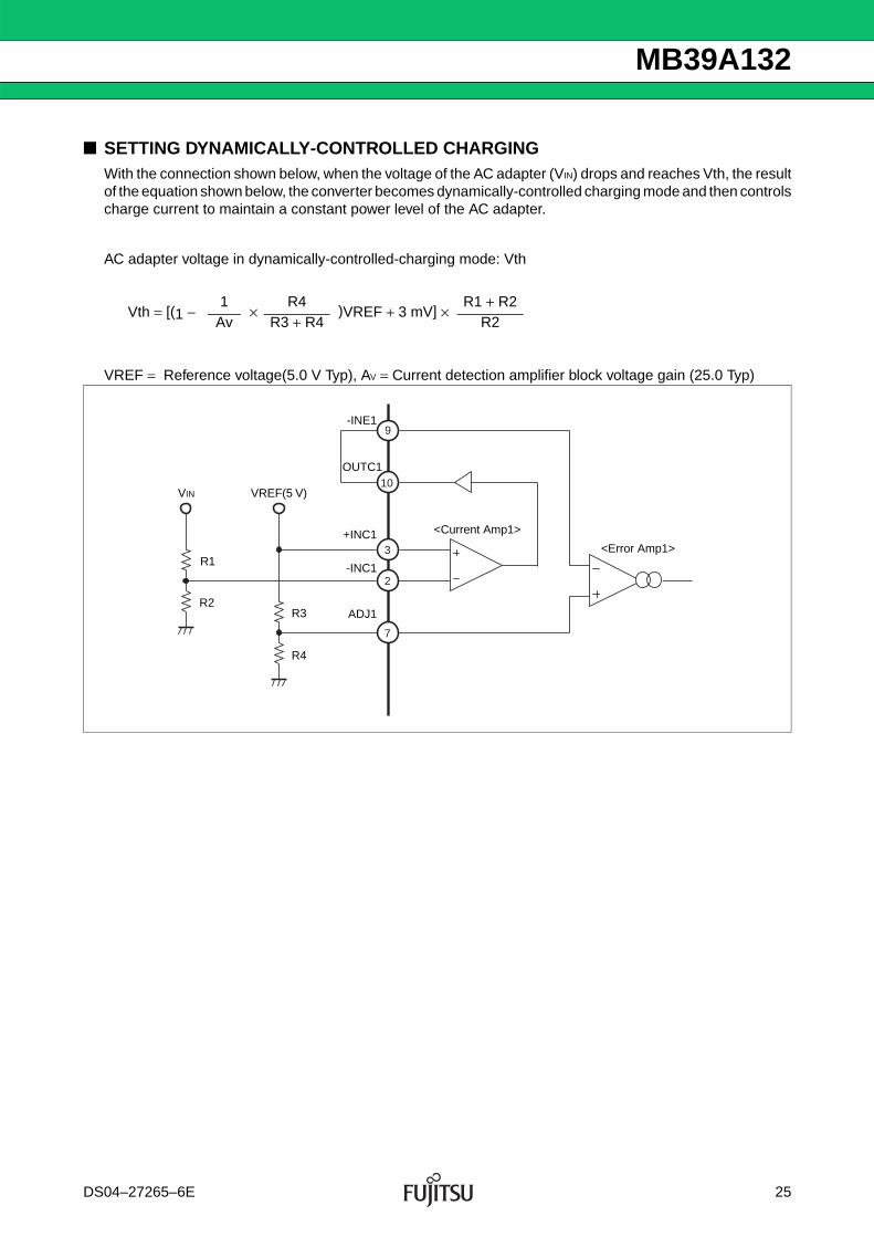
■ SETTING DYNAMICALLY-CONTROLLED CHARGINGWith the connection shown below, when the voltage of the AC adapter (VIN) drops and reaches Vth, the resultof the equation shown below, the converter becomes dynamically-controlled charging mode and then controlscharge current to maintain a constant power level of the AC adapter.
AC adapter voltage in dynamically-controlled-charging mode: Vth
VREF = Reference voltage(5.0 V Typ), AV = Current detection amplifier block voltage gain (25.0 Typ)
Vth = [(1 − 1
× R4
)VREF + 3 mV] × R1 + R2
Av R3 + R4 R2
3
7
2
10
9
VIN VREF(5 V)
R1
R2
+INC1 <Current Amp1>
<Error Amp1>
-INC1
ADJ1
OUTC1
-INE1
R3
R4
DS04–27265–6E 25
MB39A132
■ SETTING THE SOFT-START TIMETo prevent rush current at start-up of IC, the soft-start time can be set by connecting a soft-start capacitor(CS) to the CS pin (pin 19). When the CTL1 pin (pin 23) and the CTL2 pin (pin 32) are set to “H” level andthe IC is started (Vcc 3 ≥ UVLO threshold voltage), the external capacitor (Cs) for soft-start (CS) connectedto the CS pin is charged at 10 μA. The output ON duty depends on the result of comparison done by the PWM comparator among the COMP1pin (pin 8) voltage, the COMP2 pin (pin15) voltage, the COMP3 pin (pin16) voltage and the triangular waveoscillator output voltage (CT). During soft-start, the COMP1 pin, the COMP2 pin, and the COMP3 pin voltagesare clamped so that the voltages of those three pins will not exceed the CS pin voltage. Therefore, the outputvoltage of the DC/DC converter and current increase can be set by the output ON duty in proportion to riseof the CS pin voltage. The ON duty is affected by the ramp voltage of the COMP1 pin, the COMP2 pin, and the COMP3 pin untilthe output voltage of one of the three Error Amp reaches the DC/DC converter loop control voltage. Soft-start time is obtained from the following formula.
Soft-start time (time for the output ON duty to reach 80%): ts(s) := 0.23 × Cs (μF)
0V
0V
0V
0A
CTCOMP1 to COMP3CS
OUT1
Vo
Io
CS
COMP1 to COMP3
CT
OUT1
Vo
Io
Error Amp3 threshold voltage
26 DS04–27265–6E
MB39A132
■ TRANSIT RESPONSE AT STEP LOAD CHANGEThe constant voltage control loop and the constant current control loop are independent of each other .When a load changes suddenly, a control loop is replaced by the other.
Overshoot of the battery voltage and current is generated by the delay occurring in a control loop at a modechange.
The delay time is determined by the phase compensation components values.
When the constant current control changes to the constant voltage control after the battery is removed, thecontrol period with higher duty than the setting charge voltage occurs, resulting in a voltage overshoot.However, since the battery is removed, no excessive voltage is to be applied to the battery.
When the constant voltage control changes to the constant current control after the battery is inserted, thecontrol period with higher duty than the rated charge current occurs, resulting in current overshoot.
In MB39A132, a current overshoot lasting less than 10 ms is not deemed to be a current overshoot.
10 ms
When the charge control switches from the constant current control to the constant voltage control, the control period with higher duty than the rated charge voltage occurs, resulting in a voltage overshoot.
In MB39A132, a current overshoot lasting less than 10 ms is not deemed to be a current overshoot.
Error Amp3 output
Constant current Constant voltage Constant current
Error Amp2 output
Battery voltage
Battery current
Error Amp2 outputError Amp3 output
DS04–27265–6E 27
MB39A132
■ CONNECTION WITHOUT USING THE CURRENT AMP1,CURRENT AMP2 AND THE ERROR AMP1, ERROR AMP2When Current Amp1, Current Amp2 and Error Amp1, Error Amp2 are no used,• Connect the +INC1 pin (pin 3) and the -INC1 pin (pin 2) to the VREF pin (pin 21)• Connect the +INC2 pin (pin 12) and the -INC2 pin (pin 13) to the battery• Leave the OUTC1 pin (pin 10), the OUTC2 pin (pin 11), the COMP1 pin (pin 8) and the COMP2 pin
(pin 15) open• Connect the ADJ1 pin (pin 7) and the ADJ2 pin (pin 14) to the VREF pin • Connect the -INE1 pin (pin 9) to the GND pin (pin 22)
Moreover, when Current Amp1 is not used, connect the CTL2 pin (pin 32) to the GND pin (pin 22).
Fairchild : Fairchild Semiconductor International, Inc.
Com-ponent Item Specification Vendor Package Parts No. Remarks
R38 Resistor Not mounted
R39 Resistor 0 Ω KOA 1608 RK73Z1J
R40 Resistor 2.4 kΩ SSM 1608 RR0816P242D
R41 Resistor 1 kΩ SSM 1608 RR0816P102D
R42 Resistor 22 kΩ SSM 1608 RR0816P223D
R43 Resistor Not mounted
34 DS04–27265–6E
MB39A132
■ APPLICATION NOTE• Inductor selection
As a rough guide, the inductance of an inductor should keep the peak-to-peak value of inductor ripple currentbelow 50% of the maximum charge current. The inductance fulfilling the above condition can be found bythe following formula.
L : Inductance [H]
IOMAX : Maximum charge current [A]
LOR : Inductor ripple current peak to peak value - Maximum charge current ratio (0.5)
VIN : Switching power-supply voltage [V]
VO : Charge voltage [V]
fOSC : Switching frequency [Hz]
The minimum charge current (critical current) in the condition that inductor current does not flow in reversecan be found by the following formula.
IOC : Critical current [A]
L : Inductance [H]
VIN : Switching power-supply voltage [V]
VO : Charge voltage [V]
fOSC : Switching frequency [Hz]
The maximum value of the current flowing through the inductor needs to be found in order to determinewhether the current flowing through the inductor is within the rated value. The maximum current flowingthrough the inductor can be found by the following formula.
ILMAX : Maximum inductor current [A]
IOMAX : Maximum charge current [A]
ΔIL : Inductor ripple current peak to peak value [A]
L ≥ VIN − VO
× VO
LOR × IOMAX VIN × fOSC
IOC = VO
× VIN − VO
2 × L VIN × fOSC
ILMAX ≥ IoMAX + ΔIL
2
ΔIL ≥ VIN − VO
× VO
L VIN × fOSC
ΔIL
0
IoMAX
ILMAX
Inductor current
The current is shifting according to the charge current.
TimeIOC
DS04–27265–6E 35
MB39A132
• SWFET selection
If MB39A132 is used for the charger for a notebook PC, since the output voltage of an AC adapter, which isthe input voltage of an SWFET, is 25 V or less, in general, a 30 V class MOS FET can be used as the SWFET. Obtain the maximum value of the current flowing through the SWFET in order to determine whether thecurrent flowing through the SWFET is within the rated value. The maximum current flowing through theSWFET can be found by the following formula.
IDMAX : Maximum SWFET drain current [A]
IOMAX : Maximum charge current [A]
ΔIL : Inductor ripple current peak to peak value [A]
In addition, find the loss of the SWFET in order to determine whether the allowable loss of the SWFET iswithin the rated value. The allowable loss of the high-side of FET can be found by the following formula.
PHisideFET = PRON_Hiside + PSW_Hiside
PHisideFET : FET loss of high-side [W]
PRON_Hiside: FET continuity loss of high-side [W]
PSW_Hiside : FET switching loss of high-side [W]
FET continuity loss of high-side
PRON_Hiside : FET continuity loss of high-side [W]
IOMAX : Maximum charge current [A]
VIN : Switching power supply voltage [V]
VO : Output voltage [V]
RON_Hiside : FET ON resistance of high-side [Ω]
FET switching loss of high-side
PSW_Hiside : FET switching loss of high-side [W]
VIN : Switching power supply voltage [V]
fOSC : Switching frequency (Hz)
Ibtm : Bottom value of ripple current of inductor [A]
IDMAX ≥ IoMAX + ΔIL
2
PRON_Hiside = IOMAX2 × VO
× RON_HisideVIN
PSW_Hiside = VIN × fOSC × (Ibtm × Tr + Itop × Tf)
2
36 DS04–27265–6E
MB39A132
Itop : Top value of ripple current of inductor [A]
ΔIL : Inductor ripple current peak to peak value [A]
Tr : FET turn-on time of high-side [s]
Tf : FET turn-off time of high-side [s]
Tr and Tf can be easily found by the following formula.
Qgd : Gate-Drain charge of high-side FET [C]
Vgs(on) : Gate-Source voltage of high-side FET with Qgd [V]
The FET loss of the low-side can be found by the following formula.
PLosideFET : FET loss of low-side [W]
PRON_Loside : FET continuity loss of low-side [W]
IOMAX : Maximum charge current [A]
VIN : Switching power supply voltage [V]
VO : Output voltage [V]
Ron_Loside : FET ON resistance of synchronous rectification [Ω]
The FET voltage transiting between drain-source of the low-side is generally small. The SWFET loss isomitted in this document as it is negligible.
Since the power for driving gate of SWFET is supplied by LDO in IC, the SWFET allowable maximum totalgate charge (QgTotalMax) is determined by the following formula.
QgTotalMax : High-side FET allowable maximum total charge [C]
fOSC : Oscillation frequency [Hz]
Ibtm = IOMAX − ΔIL
2
Itop = IOMAX − ΔIL
2
Tr = Qgd × 4
Tf = Qgd × 1
5 − Vgs(on) Vgs(on)
PLosideFET = PRON_Loside = IOMAX2 × (1 − VO
) × Ron_LosideVIN
QgTotalMax ≤ 0.03
fOSC
DS04–27265–6E 37
MB39A132
• Fly-back diode selection
The DC/DC converter control IC needs a fly-back diode.
Select a Schottky barrier diode (SBD) that has a small forward voltage drop.
The current rating value for the fly-back diode can be calculated by the following formula.
IF : Current rating value of fly-back diode [A]
IOMAX : Maximum charge current [A]
VIN : Switching power supply voltage [V]
Vo : Charge voltage [V]
The rating of a fly-back diode can be found by the following formula.
VR_Fly > VIN
VR_Fly : DC reverse voltage of fly-back diode [V]
VIN : Switching power supply voltage [V]
IF ≥ IOMAX × (1 − Vo
)VIN
38 DS04–27265–6E
Revised the description.
MB39A132
• Output capacitor selection
Since a high ESR causes the output ripple voltage to increase, a low-ESR capacitor is needs to be used inorder to reduce the output ripple voltage. Use a capacitor that has sufficient ratings to surge current generatedwhen the battery is inserted or removed. Generally, the ceramic capacitor is used as the output capacitor.
With the switching ripple voltage taken into consideration, the minimum capacitance required can be foundby the following formula.
Co : Output capacitance [F]
ESR : Series resistance element of output capacitance [Ω]
ΔVO : Switching ripple voltage [V]
ΔIL : Inductor ripple current peak to peak value [A]
fosc : Switching frequency [Hz]
Since an overshoot occurs in the DC/DC converter output voltage when a battery being charged is removed,use a capacitor having sufficient withstand voltage. Generally, the capacitor having a rated withstand voltagehigher than the maximum input voltage is sued.
Moreover, use a capacitor having sufficient tolerance for allowable ripple current. The allowable ripple currentrequired can be found by the following formula.
Irms : Allowable ripple current (Root-mean-square value) [A]
ΔIL : Inductor ripple current peak-to-peak value [A]
Co ≥ 1
2π × fosc × (ΔVO/ΔIL − ESR)
Irms ≥ ΔIL
2√3
DS04–27265–6E 39
MB39A132
• Input capacitor selection
Select an input capacitor that has an ESR as small as possible. A ceramic capacitor is ideal. If a high-capacitance capacitor is needed for which there is no suitable ceramic capacitor use a polymer capacitor ora tantalum capacitor having a low ESR. The ripple voltage by the switching operation of the DC/DC converter is generated in the power supplyvoltage. Please consider the lower limit value of the input capacitor according to the allowable ripple voltage.The ripple voltage of the power supply can be easily found by the following formula.
ΔVIN : Switching power supply ripple voltage peak-to-peak value [V]
IOMAX : Maximum charge current [A]
CIN : Input capacitance [F]
VIN : Switching power supply voltage [V]
VO : Charge voltage [V]
fOSC : Switching frequency [Hz]
ESR : Series resistance element of input capacitance [Ω]
ΔIL : Inductor ripple current peak-to-peak value [A]
The ripple voltage of the power supply can be decreased by raising the switching frequency besides usingthe capacitor. The capacitor has its own frequency, temperature and bias voltage, therefore its effective capacitance canbe extremely small depending on the application conditions.
Select a capacitor whose rating has a sufficient margin against input voltage.In addition, when using a capacitor having an allowable ripple current rating, select a capacitor that has asufficient margin against ripple current.
The allowable ripple current can be found by the following formula.
Irms : Allowable ripple current (Root-mean-square value) [A]
IOMAX : Maximum charge current [A]
VIN : Switching power supply voltage [V]
VO : Charge voltage [V]
ΔVIN = IOMAX
× VO
+ ESR × (IOMAX + ΔIL
) CIN VIN × fOSC 2
Irms ≥ IOMAX × √VO × (VIN − VO)
VIN
40 DS04–27265–6E
MB39A132
• Bootstrap diode selection
Select a Schottky barrier diode (SBD) that has a small forward voltage drop.The current to drive the gate of High-side FET flows to the SBD of the bootstrap circuit. The average currentcan be found by the following formula. Select a bootstrap diode that keep the average current below thecurrent rating.
ID ≥ Qg × fOSC
ID : Forward current [A]
Qg : FET total gate electric charge of high-side [C]
fOSC : Oscillation frequency [Hz]
The rating of the bootstrap diode can be found by the following formula.
VR_BOOT > VIN
VR_BOOT : Bootstrap diode DC reverse voltage [V]
VIN : Switching power supply voltage [V]
• Bootstrap capacitor selection
The bootstrap capacitor needs to be sufficiently charged to drive the gate of the high-side FET. Therefore,select a capacitor that can store charge at least 10 times Qg of the high-side FET as the bootstrap capacitor.
CBOOT: Bootstrap capacitance [F]
Qg : Withstand voltage FET gate charge [C]
VB : VB voltage [V]
The rating of bootstrap capacitor can be found by the following formula.
VCBOOT > VIN
VCBOOT : Rating of bootstrap capacitor [V]
VIN : Switching power supply voltage [V]
CBOOT ≥ 10 × Qg
VB
DS04–27265–6E 41
MB39A132
• VB capacitor
Although the typical capacitance value for a VB capacitor is 1 μF, it has to be adjusted if the switching FETused has a large Qg. The bootstrap capacitor needs to be sufficiently charged to drive the gate of the high-side FET. Therefore, select a capacitor that can store charge at least 100 times the total of Qg of the high-side FET and Qg of the low-side switching FET as the VB capacitor.
CVB : VB pin capacitance [F]
Qg : Total gate charge of high-side FET and low-side switching FET [C]
VB : VB voltage [V]
The rating of VB capacitor can be found by the formula.
VCVB > VB
VCVB : Withstand voltage of VB capacitor [V]
VB :VB voltage [V]
CVB ≥ 100 × Qg
VB
42 DS04–27265–6E
MB39A132
• Design of phase compensation circuit(1) Constant voltage (CV) mode phase compensation circuit
When a low-ESR capacitor, such as a ceramic capacitor, is used as the output capacitor, it is easier for theDC/DC converter to oscillate as the phase delay approaches 180 degrees due to the resonance frequencyof LC. In this situation, perform phase compensation by connecting a RC phase lead compensator betweenthe -INE3 pin (pin 6) and the COMP3 pin (pin 16), and between the -INE3 pin (pin 6) and the BATT pin (pin 17) .
2pole-2zero phase compensation circuit
The constant for the phase lead compensation circuit can be found by the following formula.
CELLS : Number of battery series cells
fLC : Resonance frequency of inductor and output capacitor [Hz]
VIN : Switching power supply voltage [V]
fCO : Crossover frequency [Hz]
As for the crossover frequency (fco) indicating the bandwidth of the control loop of the DC/DC converter,while a high crossover frequency is good for quick response, it increases the risk of oscillation due to aninsufficient phase margin.
Though this crossover frequency can be freely set, keep the frequency in the range of 1/10-1/5 of the switchingfrequency (fosc) whenever possible.
CZ1 := 5.1 × 10 − 6
(2 × CELLS − 1) fLC
RZ2 := 8.9 × 10⁴ × fCO
+ 3600VIN × fLC
CZ2 := 1
2π × RZ2 × fLC
-
+
BATT
VO
CZ1
R1-INE3
R2Error Amp3
COMP3
Vrefint1
CZ2 RZ217 6
16 To PWM Comp.
DS04–27265–6E 43
MB39A132
(2) Constant current (CC) mode phase compensation circuit
In constant current mode, since the output capacitor impedance has little effects on the loop responsecharacteristic, connect the 1pole-1zero phase compensation circuit with the output pin (COMP2) of the erroramplifier 2 (gm amplifier).
1pole-1zero phase compensation circuit
RC and Cc of the phase lead circuit can be found by the following formula.
Rs : Charge current detection resistance [Ω]
VIN : Switching power supply voltage [V]
L : Inductor value [H]
Co : Output capacitance [F]
fCO : Crossover frequency [Hz]
RC := 1.2 × 10⁴ × fCO × L
Rs × VIN
CC := √L × Co
Rc
-
+
-
+
BATT17
12
+INC2
Rs
Current Amp2
Vrefint2Error Amp2
COMP2
Rc
Cc
15 To PWM Comp.
44 DS04–27265–6E
MB39A132
• Allowable loss, and thermal design
In general, the allowable loss and thermal design of this IC can be ignored because this IC is highly effective.However, when this IC is used with high power supply voltage, high switching frequency, high load, or hightemperature, it is necessary to take account of the allowable loss and thermal design while using this IC.
The IC internal loss (PIC) can be found by the following formula.
PIC = VCC × (ICC + Qg × fOSC )
PIC : IC internal loss [W]
VCC : Power supply voltage (VIN) [V]
ICC : Power supply current [A] (3.6 mA Max)
Qg : Total charge of all switching FET [C] (Total charge at Vgs = 5 V)
fOSC : Switching frequency [Hz]
The junction temperature (Tj) can be found by the following formula.
Tj = Ta + θja × PIC
Tj : Junction temperature [ °C]
Ta : Ambient temperature [ °C]
θja : QFN-32 package heat resistance (22.7 °C/W)
PIC : IC internal loss [W]
DS04–27265–6E 45
MB39A132
• Board layout
When designing the layout, consider the points listed below. Take account of the following points whendesigning the board layout.
- Place a GND plane on the IC mounting surface whenever possible. Connect bypass capacitors connectedto switching components to the switching GND (PGND pin), and controller components to GND (GNDpin). Separate different GND so that no large current path passes through the controller GND (GND pins).When designing the connection of the controller GND and the switching GND, make their connectionunderneath the IC. Connect PGND to the controller GND at only one point to prevent large current fromflowing to the controller GND. Connect the controller GND to PGND only at one point of PGND in orderto prevent a large current path from passing the controller GND.
- Connect to the input capacitor (CIN), SWFET, SBD, inductor (L), sense resistor (Rs), output capacitor (Co)on the surface layer. Do not connect to them via any through-hole.
- For a loop composed of input capacitors (CIN), switching FET and SBD, minimize its current loop. Whenminimizing routing and loops, give priority to this loop over others.
- Create through-holes directly next to the GND pins of the input capacitor (CIN), SBD, output capacitor(Co), and connect these pins to the GND of the inner layer.
- Place the boot strap capacitor (CBOOT) as close to the CB, LX pins as possible.
- Place the input capacitor (CIN) and high-side FET as close together as possible. Bring out the net of theLX pin from a point close to the source pin of the high-side FET. Large currents momentarily flow throughthe net of the LX pin. Use a wiring width of about 0.8 mm, and minimize the length of routing.
- Large currents momentarily flow through the nets of the OUT1, OUT2 pins, which are connected to theswitching FET gate. Use a wiring width of about 0.8 mm and minimize the length of routing.
- Place the bypass capacitor connected to VCC, VIN, VREF, and VB pins, and the resistance connectedto the RT pin as close to the respective pins as possible. Moreover, connect the bypass capacitor andthe GND pin of the fOSC:setting resistance in close proximity to the GND pin of the IC.(Strengthen the connection to the internal layer GND by making through-holes in close proximity to eachof the GND pin of the IC, terminals of bypass capacitors, terminals of the fosc setting resistors.)
- -INCx,+INCx, BATT,COMPx,RT pins is sensitive to noise. Therefore, minimize the routing of these pinsand keep them as far away from switching components as possible.
- The remote sensing (Kelvin connection) of the routing of the -INC2 and +INC2 pins are very sensitive tonoise. Therefore, make their routing close to each other and keep the routing as far away from switchingcomponents as possible.
GND
VCC
PGND
VREF
VIN
VIN
VO
PGND
RT
SBD
Co
RS
Cin
L
Connect the PGND to the GND at a single point directly under the IC.
Surface layer
Inner layer
GND routing example Example of switching components
To LX pin
Low-side FET
To +INC2 pin
To -INC2 pin
To feedback line
To BATT pin
High-side FET
46 DS04–27265–6E
MB39A132
■ REFERENCE DATAUnless otherwise specified, the measurement conditions are VIN = 19 V, Io = 2.85 A, Li+ battery 4 Cells, andTa = + 25 °C.
(Continued)
80
82
84
86
88
90
92
94
96
98
100
0.0 0.5 1.0 1.5 2.0 2.5 3.0
2 Cells
3 Cells
4 Cells
0
2
4
6
8
10
12
14
16
18
20
0.0 0.5 1.0 1.5 2.0 2.5 3.0 3.5
4 Cells
3 Cells
2 Cells
50
55
60
65
70
75
80
85
90
95
100
0 2 4 6 8 10 12 14 16 18
OUT1
20
( V )
OUT2
( V )
LX ( V )
0
20
5
0
10
0
Io = 1.5 ASW1-2 = OFF
OUT1
OUT2
LX
400 ns/div
OUT1
20
( V )
LX ( V )
OUT2 ( V )0
20
5
0
10
0
VO = 12 VSW1-2 = OFF
OUT1
OUT2
LX
400 ns/div
Conversion efficiency - Charge current(Constant voltage mode)
Charge current Io(A)
Con
vers
ion
effic
ienc
y η(
%)
Charge voltage - Charge current
Charge current Io(A)
Cha
rge
volta
ge V
o(V
)
Conversion efficiency - Charge voltage(Constant current mode)
Charge voltage Vo(V)
Con
vers
ion
effic
ienc
y η(
%)
Switching waveform(Constant voltage mode)
Switching waveform(Constant current mode)
DS04–27265–6E 47
MB39A132
(Continued)
20 ms/div
VCTL
Io
VO
SW1-2 = OFF
12
14
Vo(V)
0
10
VCTL
(V)
0
Io(A)
1
16
18
20 ms/divVCTL
Io
VO
SW1-2 = OFF14
Vo(V)
0
10
VCTL
(V)
Io(A)
1
16
18
12
0
VCTL
VO
14
12
VO
(V)
(V)
16
18
Io
0
10
20 ms/div
VCTL
SW1-2 = OFF
0
1
Io(A)
2
3
20 ms/divVCTL
Io
VO
SW1-2 = OFF
12
14
VO
(V)
0
10
VCTL
(V)
0
Io(A)
1
16
18
2
3
Start and stop(Constant voltage mode)
Start and stop(Constant voltage mode)
Start and stop (Constant current mode)
Start and stop (Constant current mode)
48 DS04–27265–6E
MB39A132
(Continued)
Io
VO
14
VO
(V)
(V)
16
18
VOUT1
VOUT2
0
10
2 ms/div
SW1-2 = OFFCV to CV
0
Io(A)
2
0
VOUT1
VOUT2
(V)
20
Io
VO
14
VO
(V)
(V)
16
18
VOUT1
VOUT2
0
10
2 ms/div
SW1-2 = OFFCV to CV
0
Io(A)
2
0
VOUT1
VOUT2
(V)
20
Io
VO
14
VO
(V)
(V)
16
18
VOUT1
VOUT2
0
10
2 ms/div
SW1-2 = OFFCV to CC
0
2
Io(A)
4
0
VOUT1
VOUT2
(V)
20
Io
VO
14
VO
(V)
(V)
16
18
VOUT1
VOUT20
10
2 ms/div
0
VOUT1
VOUT2
(V)
20
SW1-2 = OFFCC to CV
0
2
Io(A)4
Load-step response(Constant voltage mode)
Battery insertion
Load-step response(Constant voltage mode)
Battery removal
Load-step response(Constant current mode)
Battery insertion
Load-step response(Constant current mode)
Battery removal
DS04–27265–6E 49
MB39A132
■ USAGE PRECAUTION1. Do not configure the IC over the maximum ratings
If the lC is used over the maximum ratings, the LSl may be permanently damaged.It is preferable for the device to be normally operated within the recommended usage conditions. Usageoutside of these conditions can have a bad effect on the reliability of the LSI.
2. Use the devices within recommended operating conditions
The recommended operating conditions are the recommended values that guarantee the normal operationsof LSI. The electrical ratings are guaranteed when the device is used within the recommended operating conditionsand under the conditions stated for each item.
3. Printed circuit board ground lines should be set up with consideration for common impedance
4. Take appropriate measures against static electricity• Containers for semiconductor materials should have anti-static protection or be made of conductive ma-
terial.• After mounting, printed circuit boards should be stored and shipped in conductive bags or containers.• Work platforms, tools, and instruments should be properly grounded.• Working personnel should be grounded with resistance of 250 kΩ to 1 MΩ in series between body and
ground.
5. Do not apply negative voltagesThe use of negative voltages below −0.3 V may cause the parasitic transistor to be activated on LSI lines,which can cause malfunctions.
50 DS04–27265–6E
MB39A132
■ ORDERING INFORMATION
■ EV BOARD ORDERING INFORMATION
Part number Package Remarks
MB39A132WQN32-pin plastic QFN
(LCC-32P-M19)
EV board part No. EV board version No. Remarks
MB39A132EVB-02 Board rev.2.0 QFN-32
DS04–27265–6E 51
MB39A132
■ RoHS COMPLIANCE INFORMATION OF LEAD (Pb) FREE VERSIONThe LSI products of FUJITSU SEMICONDUCTOR with “E1” are compliant with RoHS Directive, and has observed the standard of lead, cadmium, mercury, hexavalent chromium, polybrominated biphenyls (PBB) , and polybrominated diphenyl ethers (PBDE) . A products whose part number has trailing characters “E1” is RoHS compliant.
■ MARKING FORMAT (LEAD-FREE VERSION)
■ LABELING SAMPLE (LEAD-FREE VERSION)
Lead-free version(E1)
INDEX
2006/03/01 ASSEMBLED IN JAPAN
G
QC PASS
(3N) 1MB123456P-789-GE1 1000
(3N)2 1561190005 107210
1,000 PCS
0605 - Z01A 10001/11561190005
MB123456P - 789 - GE1
MB123456P - 789 - GE1
MB123456P - 789 - GE1
Pb
Lead-free mark
JEITA logo JEDEC logo
The part number of a lead-free product has the trailing characters “E1”.
“ASSEMBLED IN CHINA” is printed on the label of a product assembled in China.
Before opening Please use it within two years after
Manufacture.
From opening to the 2ndreflow
Less than 8 days
When the storage period afteropening was exceeded
Please process within 8 daysafter baking (125 °C, 24H)
Storage conditions 5 °C to 30 °C, 70%RH or less (the lowest possible humidity)
260°C
(e)
(d')
(d)
255°C
170 °C
190 °C
RT (b)
(a)
(c)
to
(Note)Temperature : on the top of the package body
“H” level : 260 °C Max (a) Temperature increase gradient : Average 1 °C/s to 4 °C/s (b) Preliminary heating : Temperature 170 °C to 190 °C, 60 s to 180 s (c) Temperature increase gradient : Average 1 °C/s to 4 °C/s (d) Peak temperature : Temperature 260 °C Max; 255 °C or more, 10 s or less (d’) Main heating : Temperature 230 °C or more, 40 s or less
orTemperature 225 °C or more, 60 s or less
orTemperature 220 °C or more, 80 s or less
(e) Cooling : Natural cooling or forced cooling
Main heating
DS04–27265–6E 53
MB39A132
■ PACKAGE DIMENSIONS
Please check the latest package dimension at the following URL.http://edevice.fujitsu.com/package/en-search/
32-pin plastic QFN Lead pitch 0.50 mm
Package width ×package length
5.00 mm × 5.00 mm
Sealing method Plastic mold
Mounting height 0.80 mm MAX
Weight 0.06 g
32-pin plastic QFN(LCC-32P-M19)
(LCC-32P-M19)
(.010 )
C 2009-2010 FUJITSU SEMICONDUCTOR LIMITED C32071S-c-1-2
(.197±.004)5.00±0.10
5.00±0.10(.197±.004)
(3-R0.20)((3-R.008))
0.50(.020)1PIN CORNER(C0.30(C.012))
0.75±0.05
(0.20(.008))
INDEX AREA
0.40±0.05(.016±.002)
+0.03–0.02
–.001+.001
0.02(.001 )
(.138±.004)3.50±0.10
3.50±0.10(.138±.004)
(TYP)
(.030±.002)
+0.05–0.07
–.003+.002
0.25
Dimensions in mm (inches).Note: The values in parentheses are reference values.
54 DS04–27265–6E
MB39A132
■ MAJOR CHANGES IN THIS EDITIONA change on a page is indicated by a vertical line drawn on the left side of that page.
North and South AmericaFUJITSU SEMICONDUCTOR AMERICA, INC.1250 E. Arques Avenue, M/S 333Sunnyvale, CA 94085-5401, U.S.A.Tel: +1-408-737-5600 Fax: +1-408-737-5999http://us.fujitsu.com/micro/
KoreaFUJITSU SEMICONDUCTOR KOREA LTD.902 Kosmo Tower Building, 1002 Daechi-Dong,Gangnam-Gu, Seoul 135-280, Republic of KoreaTel: +82-2-3484-7100 Fax: +82-2-3484-7111http://kr.fujitsu.com/fsk/
Asia PacificFUJITSU SEMICONDUCTOR ASIA PTE. LTD.151 Lorong Chuan,#05-08 New Tech Park 556741 SingaporeTel : +65-6281-0770 Fax : +65-6281-0220http://sg.fujitsu.com/semiconductor/
FUJITSU SEMICONDUCTOR PACIFIC ASIA LTD.2/F, Green 18 Building, Hong Kong Science Park,Shatin, N.T., Hong KongTel : +852-2736-3232 Fax : +852-2314-4207http://cn.fujitsu.com/fsp/
Specifications are subject to change without notice. For further information please contact each office.
All Rights Reserved.The contents of this document are subject to change without notice. Customers are advised to consult with sales representatives before ordering.The information, such as descriptions of function and application circuit examples, in this document are presented solely for the purposeof reference to show examples of operations and uses of FUJITSU SEMICONDUCTOR device; FUJITSU SEMICONDUCTOR doesnot warrant proper operation of the device with respect to use based on such information. When you develop equipment incorporatingthe device based on such information, you must assume any responsibility arising out of such use of the information. FUJITSU SEMICONDUCTOR assumes no liability for any damages whatsoever arising out of the use of the information.Any information in this document, including descriptions of function and schematic diagrams, shall not be construed as license of the useor exercise of any intellectual property right, such as patent right or copyright, or any other right of FUJITSU SEMICONDUCTOR or anythird party or does FUJITSU SEMICONDUCTOR warrant non-infringement of any third-party's intellectual property right or other rightby using such information. FUJITSU SEMICONDUCTOR assumes no liability for any infringement of the intellectual property rights orother rights of third parties which would result from the use of information contained herein.The products described in this document are designed, developed and manufactured as contemplated for general use, including withoutlimitation, ordinary industrial use, general office use, personal use, and household use, but are not designed, developed and manufacturedas contemplated (1) for use accompanying fatal risks or dangers that, unless extremely high safety is secured, could have a serious effectto the public, and could lead directly to death, personal injury, severe physical damage or other loss (i.e., nuclear reaction control innuclear facility, aircraft flight control, air traffic control, mass transport control, medical life support system, missile launch control inweapon system), or (2) for use requiring extremely high reliability (i.e., submersible repeater and artificial satellite).Please note that FUJITSU SEMICONDUCTOR will not be liable against you and/or any third party for any claims or damages aris-ing in connection with above-mentioned uses of the products.Any semiconductor devices have an inherent chance of failure. You must protect against injury, damage or loss from such failuresby incorporating safety design measures into your facility and equipment such as redundancy, fire protection, and prevention of over-current levels and other abnormal operating conditions.Exportation/release of any products described in this document may require necessary procedures in accordance with the regulationsof the Foreign Exchange and Foreign Trade Control Law of Japan and/or US export control laws.The company names and brand names herein are the trademarks or registered trademarks of their respective owners.