2009-2020 Microchip Technology Inc. DS20002139E-page 1 MCP6561/1R/1U/2/4 Features • Propagation Delay at 1.8 V DD : - 56 ns (typical) high-to-low - 49 ns (typical) low-to-high • Low Quiescent Current: 100 μA (typical) • Input Offset Voltage: ±3 mV (typical) • Rail-to-Rail Input: V SS – 0.3V to V DD + 0.3V • CMOS/TTL-Compatible Output • Wide Supply Voltage Range: 1.8V to 5.5V • Available in Single, Dual and Quad • Packages: SC70, SOT-23, SOIC, MSOP, TSSOP Typical Applications • Laptop Computers • Mobile Phones • Handheld Electronics • RC Timers • Alarm and Monitoring Circuits • Window Comparators • Multivibrators Design Aids • Microchip Advanced Part Selector (MAPS) • Analog Demonstration and Evaluation Boards • Application Notes Related Devices • Open-Drain Output: MCP6566/6R/6U/7/9 Typical Application Description The Microchip Technology Inc. MCP6561/1R/1U/2/4 families of CMOS/TTL-compatible comparators are offered in single, dual and quad configurations. These comparators are optimized for low-power 1.8V, single-supply applications with greater than rail-to-rail input operation. The internal input hysteresis eliminates output switching due to internal input noise voltage, reducing current draw. The push-pull output of the MCP6561/1R/1U/2/4 family supports rail-to-rail output swing and interfaces with CMOS/TTL logic. The output toggle frequency can reach a typical of 4 MHz while limiting supply current surges and dynamic power consumption during switching. This family operates with a single-supply voltage of 1.8V to 5.5V, while drawing less than 100 μA/comparator of quiescent current (typical). Package Types V IN V OUT V DD R 2 R F R 3 V DD MCP656X – + MCP6562 +INA -INA V SS 1 2 3 4 8 7 6 5 OUTA V DD OUTB -INB +INB MCP6564 +INA -INA V SS 1 2 3 4 14 13 12 11 OUTA V DD OUTD -IND +IND 10 9 8 5 6 7 OUTB -INB +INB +INC -INC OUTC 5 4 MCP6561 1 2 3 5 4 MCP6561R 1 2 3 +IN V SS OUT -IN V DD +IN V DD OUT -IN V SS 5-Lead SOT-23, SC70 8-Lead SOIC, MSOP 5-Lead SOT-23 14-Lead SOIC, TSSOP 4 1 2 3 5 5-Lead SOT-23 V SS V IN + V IN - V DD OUT MCP6561U + – + – + – + – + – + – + – + – + – 1.8V Low-Power Push-Pull Output Comparator
• Low Quiescent Current: 100 µA (typical)• Input Offset Voltage: ±3 mV (typical)• Rail-to-Rail Input: VSS – 0.3V to VDD + 0.3V• CMOS/TTL-Compatible Output• Wide Supply Voltage Range: 1.8V to 5.5V• Available in Single, Dual and Quad• Packages: SC70, SOT-23, SOIC, MSOP, TSSOP
Typical Applications• Laptop Computers• Mobile Phones• Handheld Electronics• RC Timers• Alarm and Monitoring Circuits• Window Comparators• Multivibrators
Design Aids• Microchip Advanced Part Selector (MAPS)• Analog Demonstration and Evaluation Boards• Application Notes
Related Devices• Open-Drain Output: MCP6566/6R/6U/7/9
Typical Application
DescriptionThe Microchip Technology Inc. MCP6561/1R/1U/2/4families of CMOS/TTL-compatible comparators areoffered in single, dual and quad configurations.These comparators are optimized for low-power 1.8V,single-supply applications with greater than rail-to-railinput operation. The internal input hysteresis eliminatesoutput switching due to internal input noise voltage,reducing current draw. The push-pull output of theMCP6561/1R/1U/2/4 family supports rail-to-rail outputswing and interfaces with CMOS/TTL logic. The outputtoggle frequency can reach a typical of 4 MHz whilelimiting supply current surges and dynamic powerconsumption during switching.This family operates with a single-supply voltage of 1.8Vto 5.5V, while drawing less than 100 µA/comparator ofquiescent current (typical).
Package Types
VIN
VOUT
VDD
R2
RFR3
VDD MCP656X–
+
MCP6562
+INA-INA
VSS
1
2
3
4
8
7
6
5
OUTA VDD
OUTB-INB+INB
MCP6564
+INA-INA
VSS
1
2
3
4
14
13
12
11
OUTA
VDD
OUTD-IND+IND
10
9
8
5
6
7OUTB-INB+INB +INC
-INCOUTC
5
4
MCP6561
1
2
3
5
4
MCP6561R
1
2
3
+INVSS
OUT
-IN
VDD
+INVDD
OUT
-IN
VSS
5-Lead SOT-23, SC70 8-Lead SOIC, MSOP
5-Lead SOT-23 14-Lead SOIC, TSSOP
4
1
2
3
5
5-Lead SOT-23
VSS
VIN+
VIN-
VDD
OUT
MCP6561U
+ –+ –
+ –
+–
+ –+–+– + –
+
–
2009-2020 Microchip Technology Inc. DS20002139E-page 1
MCP6561/1R/1U/2/4
NOTES:
DS20002139E-page 2 2009-2020 Microchip Technology Inc.
MCP6561/1R/1U/2/4
1.0 ELECTRICAL
CHARACTERISTICS1.1 Absolute Maximum Ratings†VDD – VSS ...................................................................... 6.5VAnalog Input (VIN)†† .....................VSS – 1.0V to VDD + 1.0VAll Other Inputs and Outputs.........VSS – 0.3V to VDD + 0.3VDifference Input voltage ..................................... |VDD – VSS|Output Short-Circuit Current .................................... ±25 mACurrent at Input Pins .................................................. ±2 mACurrent at Output and Supply Pins .......................... ±50 mAStorage Temperature .................................. -65°C to +150°CAmbient Temp. with Power Applied ............ -40°C to +125°CJunction Temp. .......................................................... +150°CESD Protection on All Pins (HBM/MM) 4 kV/300V
† Notice: Stresses above those listed under “Maximum Ratings” may cause permanent damage to the device. This is a stress rating only and functional operation of the device at those or any other conditions above those indicated in the operational listings of this specification is not implied. Exposure to maximum rating conditions for extended periods may affect device reliability.
†† See Section 4.1.2 “Input Voltage and Current Limits”.
DC CHARACTERISTICSElectrical Characteristics: Unless otherwise indicated: VDD = +1.8V to +5.5V, VSS = GND, TA = +25°C, VIN+ = VDD/2, VIN- = VSS, RL = 10 k to VDD/2 (see Figure 1-1).
Parameters Symbol Min Typ Max Units Conditions
Power SupplySupply Voltage VDD 1.8 — 5.5 VQuiescent Current per Comparator IQ 60 100 130 µA IOUT = 0Power Supply Rejection Ratio PSRR 63 70 — dB VCM = VSS
Common-Mode Rejection Ratio CMRR 54 66 — dB VCM = -0.3V to VDD + 0.3V, VDD = 5.5V50 63 — dB VCM = VDD/2 to VDD + 0.3V, VDD = 5.5V54 65 — dB VCM = -0.3V to VDD/2, VDD = 5.5V
Common-Mode Input Impedance ZCM — 1013||4 — ||pFDifferential Input Impedance ZDIFF — 1013||2 — ||pFPush-Pull OutputHigh-Level Output Voltage VOH VDD – 0.7 — — V IOUT = -3 mA/-8 mA with VDD = 1.8V/5.5V
(Note 3)Low-Level Output Voltage VOL — — 0.6 V IOUT = 3 mA/8 mA with VDD = 1.8V/5.5V
(Note 3)Short-Circuit Current ISC — ±30 — mA Note 3Output Pin Capacitance COUT — 8 — pFNote 1: The input offset voltage is the center of the input referred trip points. The input hysteresis is the difference between the
input referred trip points.2: VHYST at different temperatures is estimated using VHYST (TA) = VHYST @ +25°C + (TA – 25°C) TC1 + (TA – 25°C)2 TC2.3: Limit the output current to the absolute maximum rating of 50 mA.
2009-2020 Microchip Technology Inc. DS20002139E-page 3
MCP6561/1R/1U/2/4
AC CHARACTERISTICS
TEMPERATURE SPECIFICATIONS
Electrical Characteristics: Unless otherwise indicated: VDD = +1.8V to +5.5V, VSS = GND, TA = +25°C, VIN+ = VDD/2, VIN- = VSS, RL = 10 k to VDD/2 and CL = 25 pF (see Figure 1-1).
Parameters Symbol Min Typ Max Units ConditionsPropagation DelayHigh-to-Low,100 mV Overdrive tPHL — 56 80 ns VCM = VDD/2, VDD = 1.8V
— 2 — MHz VDD = 1.8VInput Voltage Noise(2) ENI — 350 — µVP-P 10 Hz to 10 MHzNote 1: Propagation delay skew is defined as: tPDS = tPLH – tPHL.
2: ENI is based on SPICE simulation.
Electrical Characteristics: Unless otherwise indicated: VDD = +1.8V to +5.5V and VSS = GND.Parameters Symbol Min Typ Max Units Conditions
Temperature RangesSpecified Temperature Range TA -40 — +125 °COperating Temperature Range TA -40 — +125 °CStorage Temperature Range TA -65 — +150 °CThermal Package ResistancesThermal Resistance, 5-Lead SC70 JA — 331 — °C/WThermal Resistance, 5-Lead SOT-23 JA — 220.7 — °C/WThermal Resistance, 8-Lead SOIC JA — 149.5 — °C/WThermal Resistance, 8-Lead MSOP JA — 211 — °C/WThermal Resistance, 14-Lead SOIC JA — 95.3 — °C/WThermal Resistance, 14-Lead TSSOP JA — 100 — °C/W
DS20002139E-page 4 2009-2020 Microchip Technology Inc.
MCP6561/1R/1U/2/4
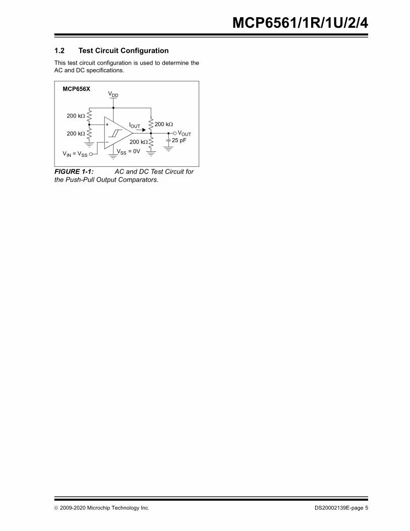
1.2 Test Circuit ConfigurationThis test circuit configuration is used to determine theAC and DC specifications.
FIGURE 1-1: AC and DC Test Circuit for the Push-Pull Output Comparators.
VDD
VSS = 0V
200 k
200 k200 k
200 kVOUT
VIN = VSS
25 pF
IOUT
MCP656X
+
–
2009-2020 Microchip Technology Inc. DS20002139E-page 5
MCP6561/1R/1U/2/4
NOTES:
DS20002139E-page 6 2009-2020 Microchip Technology Inc.
MCP6561/1R/1U/2/4
2.0 TYPICAL PERFORMANCE CURVES
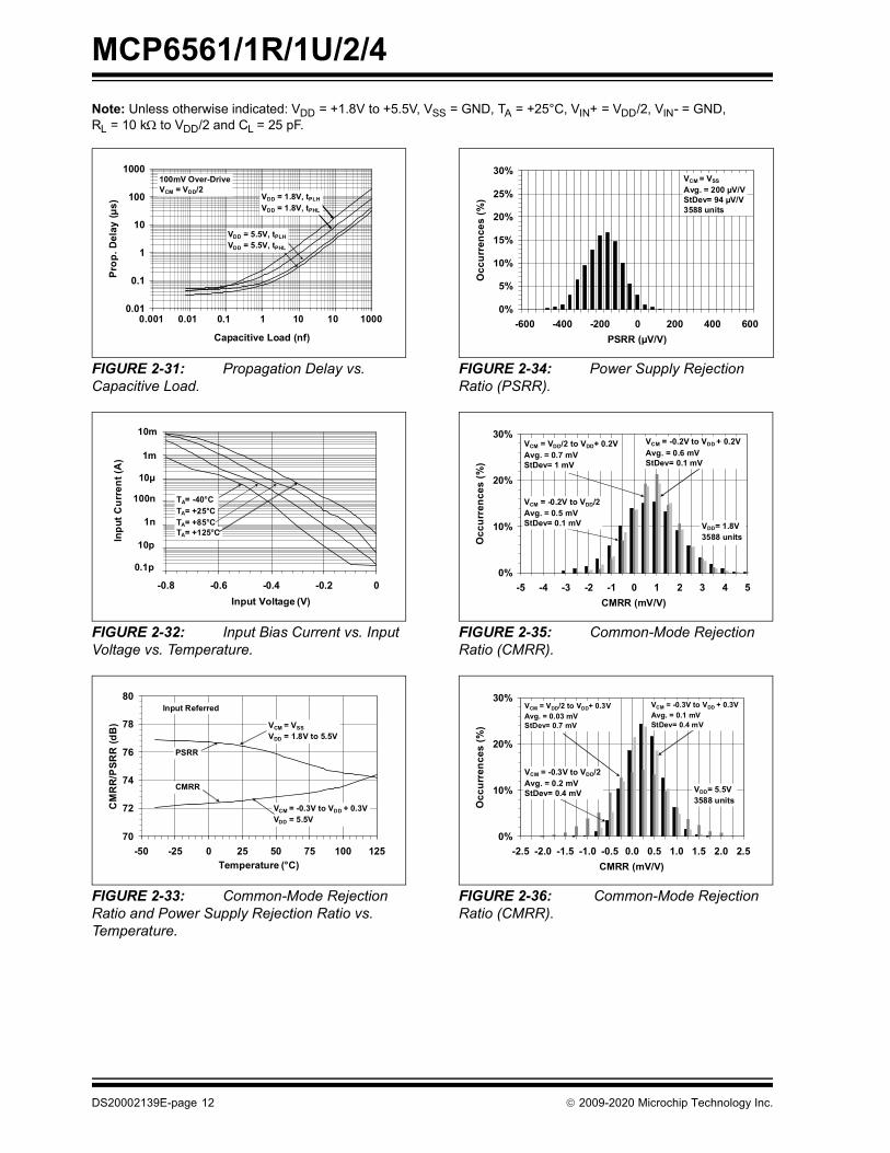
Note: Unless otherwise indicated: VDD = +1.8V to +5.5V, VSS = GND, TA = +25°C, VIN+ = VDD/2, VIN- = GND,RL = 10 k to VDD/2 and CL = 25 pF.
FIGURE 2-1: Input Offset Voltage.
FIGURE 2-2: Input Offset Voltage Drift.
FIGURE 2-3: Input vs. Output Signal, No Phase Reversal.
FIGURE 2-4: Input Hysteresis Voltage.
FIGURE 2-5: Input Hysteresis Voltage Drift – Linear Temp. Co. (TC1).
Note: The graphs and tables provided following this note are a statistical summary based on a limited number ofsamples and are provided for informational purposes only. The performance characteristics listed hereinare not tested or guaranteed. In some graphs or tables, the data presented may be outside the specifiedoperating range (e.g., outside specified power supply range) and therefore outside the warranted range.
DS20002139E-page 12 2009-2020 Microchip Technology Inc.
MCP6561/1R/1U/2/4
Note: Unless otherwise indicated: VDD = +1.8V to +5.5V, VSS = GND, TA = +25°C, VIN+ = VDD/2, VIN- = GND,RL = 10 k to VDD/2 and CL = 25 pF.
FIGURE 2-37: Output Jitter vs. Input Frequency.
FIGURE 2-38: Input Offset Current and Input Bias Current vs. Temperature.
FIGURE 2-39: Input Offset Current and Input Bias Current vs. Common-Mode Input Voltage vs. Temperature.
0.1
1
10
100
1000
10000
100 1000 10000 100000 1000000 1E+07Input Frequency (Hz)
Out
put J
itter
pk-
pk (n
s)
VDD = 5.5V
100 1k 10k 100k 1M 10M
VIN+ = 2Vpp (sine)
0.1
1
10
100
1000
25 50 75 100 125Temperature (°C)
I OS
and
I B (p
A)
IB
|IOS|
0.001
0.01
0.1
1
10
100
1000
10000
0 1 2 3 4 5 6VCM (V)
I OS
and
I B (p
A)
IB @ TA=
IB @ TA=
|IOS| @ TA= 125°C
|IOS|@ TA= 85°C
VDD = 5.5V
2009-2020 Microchip Technology Inc. DS20002139E-page 13
MCP6561/1R/1U/2/4
NOTES:
DS20002139E-page 14 2009-2020 Microchip Technology Inc.
MCP6561/1R/1U/2/4
3.0 PIN DESCRIPTIONSDescriptions of the pins are listed in Table 3-1.
TABLE 3-1: PIN FUNCTION TABLE
3.1 Analog InputsThe comparator noninverting and inverting inputs arehigh-impedance CMOS inputs with low bias currents.
3.2 Digital OutputsThe comparator outputs are CMOS push-pull, digitaloutputs. They are designed to be compatible withCMOS and TTL logic, and are capable of driving heavyDC or capacitive loads.
3.3 Power Supply (VSS and VDD)The positive power supply pin (VDD) is 1.8V to 5.5Vhigher than the negative power supply pin (VSS). Fornormal operation, the other pins are at voltagesbetween VSS and VDD.Typically, these parts are used in a single (positive)supply configuration. In this case, VSS is connected toground and VDD is connected to the supply. VDD willneed a local bypass capacitor (typically 0.01 µF to0.1 µF) within 2 mm of the VDD pin. These pins canshare a bulk capacitor with nearby analog parts (within100 mm), but it is not required.
2009-2020 Microchip Technology Inc. DS20002139E-page 15
MCP6561/1R/1U/2/4
NOTES:
DS20002139E-page 16 2009-2020 Microchip Technology Inc.
MCP6561/1R/1U/2/4
4.0 APPLICATION INFORMATIONThe MCP6561/1R/1U/2/4 families of push-pull outputcomparators are fabricated on Microchip’s state-of-the-art CMOS process. They are suitable for a wide rangeof high-speed applications requiring low-powerconsumption.
4.1 Comparator Inputs4.1.1 NORMAL OPERATIONThe input stage of these families of devices uses threedifferential input stages in parallel: one operates at lowinput voltages, one at high input voltages and one atmiddle input voltages. With this topology, the input voltagerange is 0.3V above VDD and 0.3V below VSS, while pro-viding low offset voltage throughout the Common-moderange. The input offset voltage is measured at bothVSS – 0.3V and VDD + 0.3V to ensure proper operation.The MCP6561/1R/1U/2/4 families have internally sethysteresis VHYST that is small enough to maintain inputoffset accuracy and large enough to eliminate outputchattering caused by the comparator’s own input noisevoltage, ENI. Figure 4-1 depicts this behavior. Inputoffset voltage (VOS) is the center (average) of the (inputreferred) low-high and high-low trip points. Inputhysteresis voltage (VHYST) is the difference betweenthe same trip points.
FIGURE 4-1: The MCP6561/1R/1U/2/4 Comparators’ Internal Hysteresis Eliminates Output Chatter Caused by Input Noise Voltage.
4.1.2 INPUT VOLTAGE AND CURRENT LIMITS
The ESD protection on the inputs can be depicted asshown in Figure 4-2. This structure was chosen toprotect the input transistors, and to minimize input biascurrent (IB). The input ESD diodes clamp the inputswhen they try to go more than one diode drop belowVSS. They also clamp any voltages that go too farabove VDD. Their breakdown voltage is high enough toallow normal operation and low enough to bypass ESDevents within the specified limits.
FIGURE 4-2: Simplified Analog Input ESD Structures.In order to prevent damage and/or improper operationof these amplifiers, the circuits they are in must limit thecurrents (and voltages) at the VIN+ and VIN- pins (seeSection 1.1 “Absolute Maximum Ratings†” at thebeginning of Section 1.0 “Electrical Characteris-tics”). Figure 4-3 shows the recommended approachto protecting these inputs. The internal ESD diodesprevent the input pins (VIN+ and VIN-) from going too farbelow ground, and the resistors, R1 and R2, limit thepossible current drawn out of the input pin. Diodes, D1and D2, prevent the input pin (VIN+ and VIN-) fromgoing too far above VDD. When implemented asshown, resistors, R1 and R2, also limit the currentthrough D1 and D2.
FIGURE 4-3: Protecting the Analog Inputs.It is also possible to connect the diodes to the left of theresistors, R1 and R2. In this case, the currents throughthe diodes, D1 and D2, need to be limited by some othermechanism. The resistor then serves as an inrushcurrent limiter; the DC current into the input pins (VIN+and VIN-) should be very small.
-3-2-1012345678
Time (100 ms/div)
Out
put V
olta
ge (V
)
-30-25-20-15-10-50510152025
Inpu
t Vol
tage
(10
mV/
div)
VOUT
VIN–
VDD = 5.0V
Hysteresis
BondPad
BondPad
BondPad
VDD
VIN+
VSS
InputStage
BondPad
VIN-
V1R1
VDD
D1
R2 VSS – (minimum expected V2)
2 mA
VOUT
V2R2 R3
D2
+
–
R1 VSS – (minimum expected V1)
2 mA
MCP656X
2009-2020 Microchip Technology Inc. DS20002139E-page 17
MCP6561/1R/1U/2/4
A significant amount of current can flow out of theinputs when the Common-mode voltage (VCM) is belowground (VSS); see Figure 2-32. Applications that arehigh-impedance may need to limit the usable voltagerange.
4.1.3 PHASE REVERSALThe MCP6561/1R/1U/2/4 comparator families useCMOS transistors at the input. They are designed toprevent phase inversion when the input pins exceedthe supply voltages. Figure 2-3 shows an input voltageexceeding both supplies with no resulting phaseinversion.
4.2 Push-Pull OutputThe push-pull output is designed to be compatible withCMOS and TTL logic, while the output transistors areconfigured to give rail-to-rail output performance. Theyare driven with circuitry that minimizes any switchingcurrent (shoot-through current from supply-to-supply)when the output is transitioned from high-to-low or fromlow-to-high (see Figure 2-15 and Figure 2-18 for moreinformation).
4.3 Externally Set HysteresisGreater flexibility in selecting hysteresis (or input trippoints) is achieved by using external resistors.Hysteresis reduces output chattering when one input isslowly moving past the other. It also helps in systemswhere it is best not to cycle between high and lowstates too frequently (e.g., air conditioner thermostaticcontrol). Output chatter also increases the dynamicsupply current.
4.3.1 NONINVERTING CIRCUITFigure 4-4 shows a noninverting circuit for single-supply applications using just two resistors. Theresulting hysteresis diagram is shown in Figure 4-5.
FIGURE 4-4: Noninverting Circuit with Hysteresis for Single Supply.
FIGURE 4-5: Hysteresis Diagram for the Noninverting Circuit.
The trip points for Figure 4-4 and Figure 4-5 are:
EQUATION 4-1:
VREF
VIN
VOUT
VDD
R1 RF
+
–
MCP656X
VOUT
High-to-Low Low-to-High
VDDVOH
VOLVSS
VSS VDDVTHL VTLH
VIN
VTLH VREF 1R1RF-------+
VOLR1RF-------
–=
VTHL VREF 1R1RF-------+
VOHR1RF-------
–=
Where:
VTLH = Trip Voltage from Low-to-HighVTHL = Trip Voltage from High-to-Low
DS20002139E-page 18 2009-2020 Microchip Technology Inc.
MCP6561/1R/1U/2/4
4.3.2 INVERTING CIRCUITFigure 4-6 shows an inverting circuit for single supplyusing three resistors. The resulting hysteresis diagramis shown in Figure 4-7.
FIGURE 4-6: Inverting Circuit with Hysteresis.
FIGURE 4-7: Hysteresis Diagram for the Inverting Circuit.In order to determine the trip voltages (VTHL and VTLH)for the circuit shown in Figure 4-6, R2 and R3 can besimplified to the Thevenin equivalent circuit withrespect to VDD, as shown in Figure 4-8.
FIGURE 4-8: Thevenin Equivalent Circuit.
Where:
Using this simplified circuit, the trip voltage can becalculated using the following equation:
EQUATION 4-2:
Figure 2-20, and Figure 2-23 can be used to determinetypical values for VOH and VOL.
4.4 Bypass CapacitorsWith this family of comparators, the power supply pin(VDD for single supply) should have a local bypasscapacitor (i.e., 0.01 µF to 0.1 µF) within 2 mm for goodedge rate performance.
4.5 Capacitive LoadsReasonable capacitive loads (e.g., logic gates) havelittle impact on propagation delay (see Figure 2-31).The supply current increases with increasing togglefrequency (Figure 2-19), especially with higher capaci-tive loads. The output slew rate and propagation delayperformance will be reduced with higher capacitiveloads.
VIN
VOUT
VDD
R2
RFR3
VDD MCP656X
–
+
VOUT
High-to-LowLow-to-High
VDDVOH
VOLVSS
VSS VDDVTLH VTHL
VIN
V23
VOUT
VDD
R23 RF
+
–
VSS
MCP656X
R23R2R3
R2 R3+-------------------=
V23R3
R2 R3+------------------- VDD=
VTHL VOHR23
R23 RF+-----------------------
V23RF
R23 RF+---------------------- +=
VTLH VOLR23
R23 RF+-----------------------
V23RF
R23 RF+---------------------- +=
Where:
VTLH = Trip Voltage from Low-to-HighVTHL = Trip Voltage from High-to-Low
2009-2020 Microchip Technology Inc. DS20002139E-page 19
MCP6561/1R/1U/2/4
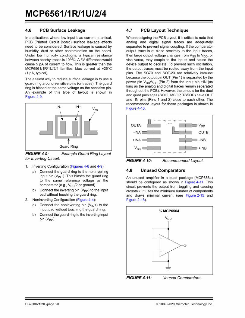
4.6 PCB Surface LeakageIn applications where low input bias current is critical,PCB (Printed Circuit Board) surface leakage effectsneed to be considered. Surface leakage is caused byhumidity, dust or other contamination on the board.Under low humidity conditions, a typical resistancebetween nearby traces is 1012. A 5V difference wouldcause 5 pA of current to flow. This is greater than theMCP6561/1R/1U/2/4 families’ bias current at +25°C(1 pA, typical).The easiest way to reduce surface leakage is to use aguard ring around sensitive pins (or traces). The guardring is biased at the same voltage as the sensitive pin.An example of this type of layout is shown inFigure 4-9.
FIGURE 4-9: Example Guard Ring Layout for Inverting Circuit.
1. Inverting Configuration (Figures 4-6 and 4-9):a) Connect the guard ring to the noninverting
input pin (VIN+). This biases the guard ringto the same reference voltage as thecomparator (e.g., VDD/2 or ground).
b) Connect the inverting pin (VIN-) to the inputpad without touching the guard ring.
2. Noninverting Configuration (Figure 4-4):a) Connect the noninverting pin (VIN+) to the
input pad without touching the guard ring.b) Connect the guard ring to the inverting input
pin (VIN-).
4.7 PCB Layout TechniqueWhen designing the PCB layout, it is critical to note thatanalog and digital signal traces are adequatelyseparated to prevent signal coupling. If the comparatoroutput trace is at close proximity to the input traces,then large output voltage changes from VSS to VDD, orvisa versa, may couple to the inputs and cause thedevice output to oscillate. To prevent such oscillation,the output traces must be routed away from the inputpins. The SC70 and SOT-23 are relatively immunebecause the output pin OUT (Pin 1) is separated by thepower pin VDD/VSS (Pin 2) from the input pin +IN (aslong as the analog and digital traces remain separatedthroughout the PCB). However, the pinouts for the dualand quad packages (SOIC, MSOP, TSSOP) have OUTand -IN pins (Pins 1 and 2) close to each other. Therecommended layout for these packages is shown inFigure 4-10.
FIGURE 4-10: Recommended Layout.
4.8 Unused ComparatorsAn unused amplifier in a quad package (MCP6564)should be configured as shown in Figure 4-11. Thiscircuit prevents the output from toggling and causingcrosstalk. It uses the minimum number of componentsand draws minimal current (see Figure 2-15 andFigure 2-18).
FIGURE 4-11: Unused Comparators.
Guard Ring
VSSIN- IN+
-INA
+INA -INB
+INB
OUTB
OUTA
VSS
VDD
VDD
–
+
¼ MCP6564
DS20002139E-page 20 2009-2020 Microchip Technology Inc.
MCP6561/1R/1U/2/4
4.9 Typical Applications
4.9.1 PRECISE COMPARATORSome applications require higher DC precision. Aneasy way to solve this problem is to use an amplifier(such as the MCP6291) to gain-up the input signalbefore it reaches the comparator. Figure 4-12 showsan example of this approach.
FIGURE 4-12: Precise Inverting Comparator.
4.9.2 WINDOWED COMPARATORFigure 4-13 shows one approach to designing awindowed comparator. The AND gate produces a logic‘1’ when the input voltage is between VRB and VRT(where VRT > VRB).
FIGURE 4-13: Windowed Comparator.
4.9.3 BISTABLE MULTIVIBRATOR
A simple bistable multivibrator design is shown inFigure 4-14. VREF needs to be between the powersupplies (VSS = GND and VDD) to achieve oscillation.The output duty cycle changes with VREF.
FIGURE 4-14: Bistable Multivibrator.
VREF
VDD
VDD
R1 R2 VOUT
VIN
VREF
MCP6291
MCP656X
+
–
+
–
VRT
VRB
VIN
VDD
1/2 MCP6562
1/2 MCP6562
+
–
+
–
VDD
R1 R2
R3
VREF
C1
VOUTMCP6561+
–
2009-2020 Microchip Technology Inc. DS20002139E-page 21
MCP6561/1R/1U/2/4
NOTES:
DS20002139E-page 22 2009-2020 Microchip Technology Inc.
MCP6561/1R/1U/2/4
5.0 DESIGN AIDS
5.1 Microchip Advanced Part Selector (MAPS)
MAPS is a software tool that helps semiconductorprofessionals efficiently identify Microchip devices thatfit a particular design requirement. Available at no costfrom the Microchip website at www.microchip.com/maps, the MAPS is an overall selection tool forMicrochip’s product portfolio that includes Analog,Memory, MCUs and DSCs. Using this tool you candefine a filter to sort features for a parametric search ofdevices and export side-by-side technical comparisonreports. Helpful links are also provided for data sheets,purchase and sampling of Microchip parts.
5.2 Analog Demonstration and Evaluation Boards
Microchip offers a broad spectrum of AnalogDemonstration and Evaluation Boards that aredesigned to help you achieve faster time to market. Fora complete listing of these boards and theircorresponding user’s guides and technical information,visit the Microchip website at www.microchip.com/analogtools. Three of our boards that are especiallyuseful are:• 8-Pin SOIC/MSOP/TSSOP/DIP Evaluation Board,
5.3 Application NotesThe following Microchip Application Note is availableon the Microchip website at www.microchip.com and isrecommended as a supplemental reference resource:• AN895, “Oscillator Circuits For RTD Temperature
Sensors”, DS00895
2009-2020 Microchip Technology Inc. DS20002139E-page 23
DS20002139E-page 24 2009-2020 Microchip Technology Inc.
MCP6561/1R/1U/2/4
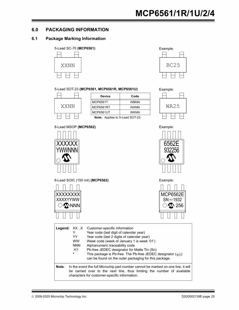
6.0 PACKAGING INFORMATION
6.1 Package Marking Information
Legend: XX...X Customer-specific informationY Year code (last digit of calendar year)YY Year code (last 2 digits of calendar year)WW Week code (week of January 1 is week ‘01’)NNN Alphanumeric traceability code Pb-free JEDEC designator for Matte Tin (Sn)* This package is Pb-free. The Pb-free JEDEC designator ( )
can be found on the outer packaging for this package.
Note: In the event the full Microchip part number cannot be marked on one line, it willbe carried over to the next line, thus limiting the number of availablecharacters for customer-specific information.
2009-2020 Microchip Technology Inc. DS20002139E-page 25
MCP6561/1R/1U/2/4
Package Marking Information (Continued)
3e
XXXXXXXXXXX
14-Lead SOIC (150 mil) (MCP6564)
XXXXXXXXXXXYYWWNNN
MCP6564
Example:
E/SL1932256
XXXXXXXX
14-Lead TSSOP (MCP6564)
YYWWNNN
MCP6564E
Example:
1932256
DS20002139E-page 26 2009-2020 Microchip Technology Inc.
MCP6561/1R/1U/2/4
0.15 C
0.15 C
0.10 C A B
CSEATING
PLANE
13
4
2X
TOP VIEW
SIDE VIEW
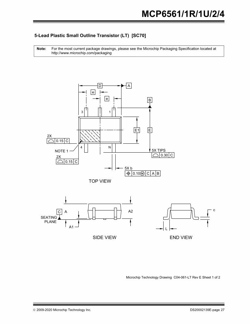
Microchip Technology Drawing C04-061-LT Rev E Sheet 1 of 2
2X
For the most current package drawings, please see the Microchip Packaging Specification located athttp://www.microchip.com/packaging
Note:
5-Lead Plastic Small Outline Transistor (LT) [SC70]
D
EE1
e
e
5X b
0.30 C5X TIPS
END VIEW
B
A
N
A
A1
A2
L
c
NOTE 1
2009-2020 Microchip Technology Inc. DS20002139E-page 27
MCP6561/1R/1U/2/4
Microchip Technology Drawing C04-061-LT Rev E Sheet 2 of 2
Number of Pins
Overall Height
Terminal Width
Overall Width
Terminal Length
Molded Package Width
Molded Package Thickness
Pitch
Standoff
UnitsDimension Limits
A1A
bE1
A2
e
L
E
N0.65 BSC
0.100.15
0.800.00
-0.20
1.25 BSC
--
2.10 BSC
MILLIMETERSMIN NOM
5
0.460.40
1.100.10
MAX
c -0.08 0.26
REF: Reference Dimension, usually without tolerance, for information purposes only.BSC: Basic Dimension. Theoretically exact value shown without tolerances.
Lead Thickness
5-Lead Plastic Small Outline Transistor (LT) [SC70]
For the most current package drawings, please see the Microchip Packaging Specification located athttp://www.microchip.com/packaging
Note:
Overall Length D 2.00 BSC0.80 - 1.00
1.Notes:
Pin 1 visual index feature may vary, but must be located within the hatched area.2. Dimensions D and E1 do not include mold flash or protrusions. Mold flash or
protrusions shall not exceed 0.15mm per side.3. Dimensioning and tolerancing per ASME Y14.5M
DS20002139E-page 28 2009-2020 Microchip Technology Inc.
MCP6561/1R/1U/2/4
RECOMMENDED LAND PATTERN
Microchip Technology Drawing No. C04-2061-LT Rev E
5-Lead Plastic Small Outline Transistor (LT) [SC70]
12
BSC: Basic Dimension. Theoretically exact value shown without tolerances.
Notes:Dimensioning and tolerancing per ASME Y14.5M1.
For the most current package drawings, please see the Microchip Packaging Specification located athttp://www.microchip.com/packaging
Note:
Dimension LimitsUnits
CContact Pad SpacingContact Pad Width
Contact Pitch
X
MILLIMETERS
0.65 BSCMIN
EMAX
Distance Between PadsContact Pad Length
GY 0.95
GxDistance Between Pads 0.20
NOM
0.452.20
1.25
X
Y
E
C
Gx
G
3
4 5
SILK SCREEN
2009-2020 Microchip Technology Inc. DS20002139E-page 29
MCP6561/1R/1U/2/4
0.15 C D2X
NOTE 1 1 2
N
TOP VIEW
SIDE VIEW
Microchip Technology Drawing C04-091-OT Rev F Sheet 1 of 2
For the most current package drawings, please see the Microchip Packaging Specification located athttp://www.microchip.com/packaging
Note:
0.20 C
C
SEATING PLANE
A A2
A1
e
NX bB0.20 C A-B D
e1
D
E1
E1/2
E/2
E
DA
0.20 C 2X
(DATUM D)(DATUM A-B)
A
ASEE SHEET 2
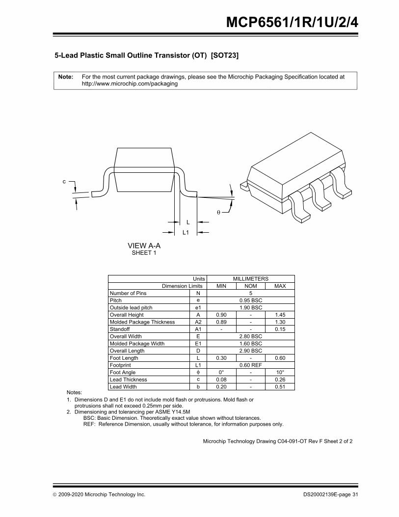
5-Lead Plastic Small Outline Transistor (OT) [SOT23]
DS20002139E-page 30 2009-2020 Microchip Technology Inc.
MCP6561/1R/1U/2/4
Microchip Technology Drawing C04-091-OT Rev F Sheet 2 of 2
For the most current package drawings, please see the Microchip Packaging Specification located athttp://www.microchip.com/packaging
Note:
c
L
L1
VIEW A-ASHEET 1
5-Lead Plastic Small Outline Transistor (OT) [SOT23]
protrusions shall not exceed 0.25mm per side.1.
BSC: Basic Dimension. Theoretically exact value shown without tolerances.2.
Foot Angle
Number of PinsPitchOutside lead pitchOverall HeightMolded Package ThicknessStandoffOverall WidthMolded Package WidthOverall LengthFoot LengthFootprint
Lead ThicknessLead Width
Notes:
L1
bc
Dimension Limits
EE1DL
e1AA2A1
Units
Ne
0°0.080.20 -
--
10°0.260.51
MILLIMETERS
0.95 BSC1.90 BSC
0.30
0.900.89
-
0.60 REF
2.90 BSC-
2.80 BSC1.60 BSC
--
-
MIN5
NOM
1.451.300.15
0.60
MAX
REF: Reference Dimension, usually without tolerance, for information purposes only.
Dimensions D and E1 do not include mold flash or protrusions. Mold flash or
Dimensioning and tolerancing per ASME Y14.5M
2009-2020 Microchip Technology Inc. DS20002139E-page 31
MCP6561/1R/1U/2/4
RECOMMENDED LAND PATTERN
5-Lead Plastic Small Outline Transistor (OT) [SOT23]
For the most current package drawings, please see the Microchip Packaging Specification located athttp://www.microchip.com/packaging
Note:
BSC: Basic Dimension. Theoretically exact value shown without tolerances.
Notes:1. Dimensioning and tolerancing per ASME Y14.5M
Microchip Technology Drawing No. C04-2091-OT Rev F
Dimension Limits
Contact Pad Length (X5)
Overall Width
Distance Between Pads
Contact Pad Width (X5)
Contact PitchContact Pad Spacing
3.90
1.10G
Z
Y1.70
0.60
MAXMIN
CX
E
UnitsNOM
0.95 BSC2.80
MILLIMETERS
Distance Between Pads GX 0.35
1
5
X
Y
Z C
E
GX
G
2
SILK SCREEN
DS20002139E-page 32 2009-2020 Microchip Technology Inc.
MCP6561/1R/1U/2/4
Note: For the most current package drawings, please see the Microchip Packaging Specification located at http://www.microchip.com/packaging
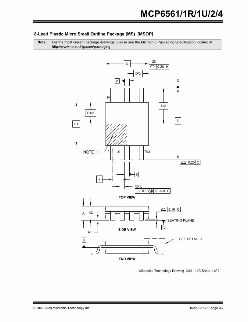
2009-2020 Microchip Technology Inc. DS20002139E-page 33
MCP6561/1R/1U/2/4
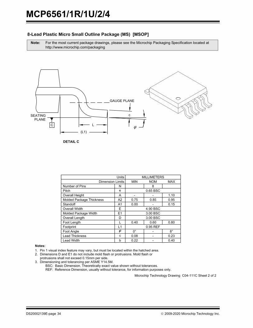
Note: For the most current package drawings, please see the Microchip Packaging Specification located at http://www.microchip.com/packaging
DS20002139E-page 34 2009-2020 Microchip Technology Inc.
MCP6561/1R/1U/2/4
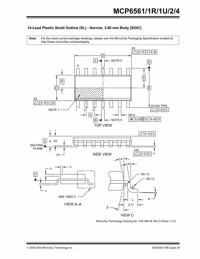
Note: For the most current package drawings, please see the Microchip Packaging Specification located at http://www.microchip.com/packaging
2009-2020 Microchip Technology Inc. DS20002139E-page 35
MCP6561/1R/1U/2/4
0.25 C A–B D
CSEATING
PLANE
TOP VIEW
SIDE VIEW
VIEW A–A
0.10 C
0.10 C
Microchip Technology Drawing No. C04-057-SN Rev E Sheet 1 of 2
8X
For the most current package drawings, please see the Microchip Packaging Specification located athttp://www.microchip.com/packaging
Note:
8-Lead Plastic Small Outline (SN) - Narrow, 3.90 mm (.150 In.) Body [SOIC]
1 2
N
h
h
A1
A2A
A
B
e
D
E
E2
E12
E1
NOTE 5
NOTE 5
NX b
0.10 C A–B2X
H 0.23
(L1)L
R0.13
R0.13
VIEW C
SEE VIEW C
NOTE 1
D
DS20002139E-page 36 2009-2020 Microchip Technology Inc.
MCP6561/1R/1U/2/4
Microchip Technology Drawing No. C04-057-SN Rev E Sheet 2 of 2
8-Lead Plastic Small Outline (SN) - Narrow, 3.90 mm (.150 In.) Body [SOIC]
For the most current package drawings, please see the Microchip Packaging Specification located athttp://www.microchip.com/packaging
protrusions shall not exceed 0.15mm per side.3. Dimensions D and E1 do not include mold flash or protrusions. Mold flash or
REF: Reference Dimension, usually without tolerance, for information purposes only.BSC: Basic Dimension. Theoretically exact value shown without tolerances.
1. Pin 1 visual index feature may vary, but must be located within the hatched area.2. § Significant Characteristic
4. Dimensioning and tolerancing per ASME Y14.5M
Notes:
§
Footprint L1 1.04 REF
5. Datums A & B to be determined at Datum H.
2009-2020 Microchip Technology Inc. DS20002139E-page 37
MCP6561/1R/1U/2/4
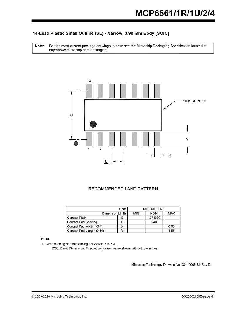
RECOMMENDED LAND PATTERN
Microchip Technology Drawing C04-2057-SN Rev E
8-Lead Plastic Small Outline (SN) - Narrow, 3.90 mm Body [SOIC]
BSC: Basic Dimension. Theoretically exact value shown without tolerances.
Notes:Dimensioning and tolerancing per ASME Y14.5M1.
For the most current package drawings, please see the Microchip Packaging Specification located athttp://www.microchip.com/packaging
Note:
Dimension LimitsUnits
CContact Pad SpacingContact Pitch
MILLIMETERS
1.27 BSCMIN
EMAX
5.40
Contact Pad Length (X8)Contact Pad Width (X8)
Y1X1
1.550.60
NOM
E
X1
C
Y1
SILK SCREEN
DS20002139E-page 38 2009-2020 Microchip Technology Inc.
MCP6561/1R/1U/2/4
Microchip Technology Drawing No. C04-065-SL Rev D Sheet 1 of 2
For the most current package drawings, please see the Microchip Packaging Specification located athttp://www.microchip.com/packaging
Note:
14-Lead Plastic Small Outline (SL) - Narrow, 3.90 mm Body [SOIC]
0.20 C
0.25 C A–B D
1 2
N
2X N/2 TIPS
TOP VIEW
SIDE VIEW
VIEW A–A
A
e
B
E
D
E2
D
E1
E22
NX b
A1
A2ACSEATING
PLANE
0.10 C14X
0.10 C A–B
0.10 C D
c
hh
H
SEE VIEW C
(L1)L
R0.13R0.13
VIEW C
NOTE 1 3
0.10 C
NOTE 5
NOTE 5
2X
2X
2009-2020 Microchip Technology Inc. DS20002139E-page 39
MCP6561/1R/1U/2/4
Microchip Technology Drawing No. C04-065-SL Rev D Sheet 2 of 2
14-Lead Plastic Small Outline (SL) - Narrow, 3.90 mm Body [SOIC]
For the most current package drawings, please see the Microchip Packaging Specification located athttp://www.microchip.com/packaging
or protrusion, which shall not exceed 0.25 mm per side.
3.
REF: Reference Dimension, usually without tolerance, for information purposes only.BSC: Basic Dimension. Theoretically exact value shown without tolerances.
1.2.
4.
Notes:
Dimension D does not include mold flash, protrusions or gate burrs, which shall
Pin 1 visual index feature may vary, but must be located within the hatched area.§ Significant Characteristic
Dimensioning and tolerancing per ASME Y14.5M
not exceed 0.15 mm per end. Dimension E1 does not include interlead flash
5. Datums A & B to be determined at Datum H.
Lead Angle 0° - -
DS20002139E-page 40 2009-2020 Microchip Technology Inc.
MCP6561/1R/1U/2/4
RECOMMENDED LAND PATTERN
Dimension LimitsUnits
Contact Pitch
MILLIMETERS
1.27 BSCMIN
EMAX
Contact Pad Length (X14)Contact Pad Width (X14)
YX
1.550.60
NOM
CContact Pad Spacing 5.40
BSC: Basic Dimension. Theoretically exact value shown without tolerances.
Notes:Dimensioning and tolerancing per ASME Y14.5M1.
For the most current package drawings, please see the Microchip Packaging Specification located athttp://www.microchip.com/packaging
Note:
E
X
Y
C
SILK SCREEN
Microchip Technology Drawing No. C04-2065-SL Rev D
14-Lead Plastic Small Outline (SL) - Narrow, 3.90 mm Body [SOIC]
1 2
14
2009-2020 Microchip Technology Inc. DS20002139E-page 41
MCP6561/1R/1U/2/4
TOP VIEW
VIEW A–A
SIDE VIEW
Sheet 1 of 2
Note:http://www.microchip.com/packagingFor the most current package drawings, please see the Microchip Packaging Specification located at
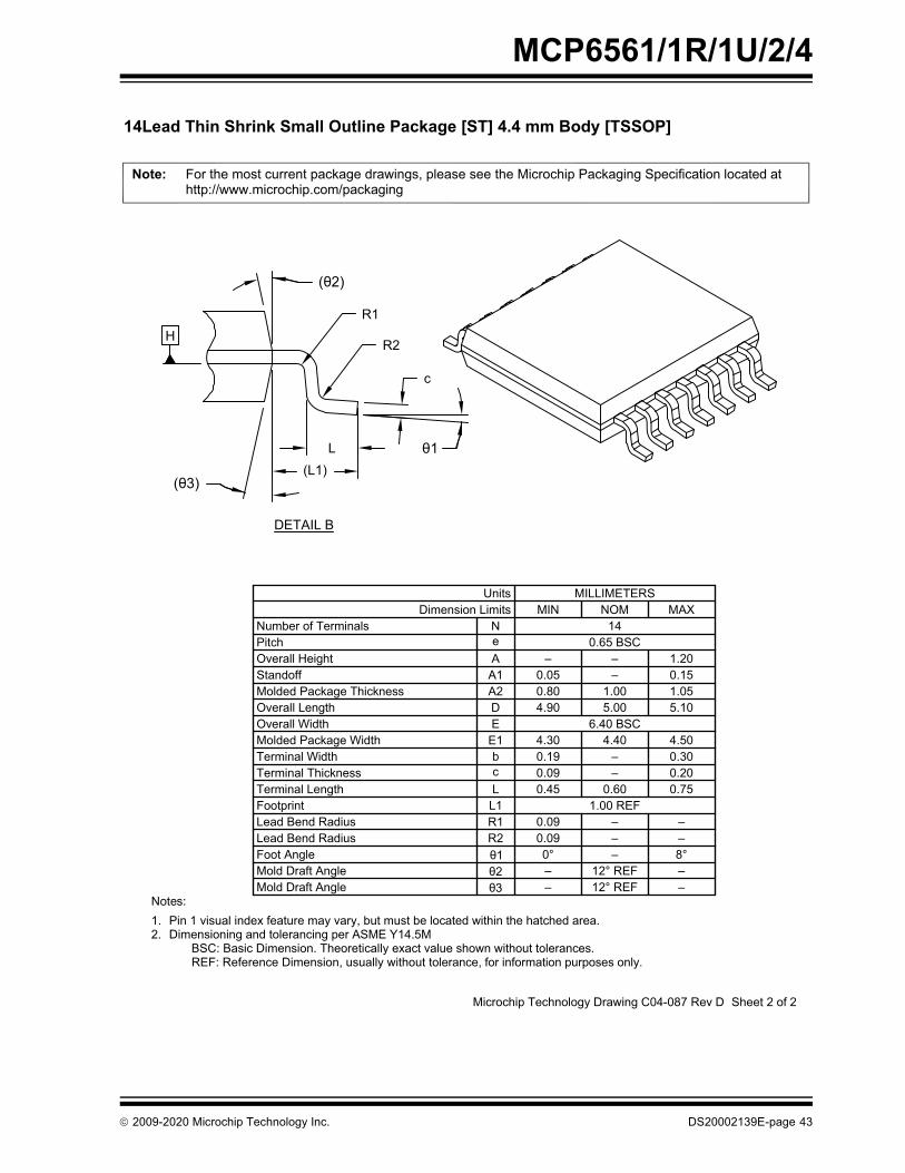
14Lead Thin Shrink Small Outline Package [ST] 4.4 mm Body [TSSOP]
Microchip Technology Drawing C04-087 Rev D
A B
CSEATING
PLANE
0.20 C B A2X 7 TIPS
0.10 C14X
0.10 C B A
A
A
1 2
N
SEE DETAIL B
D
E
E2
E1
E12
e
AA2
A114X b
DS20002139E-page 42 2009-2020 Microchip Technology Inc.
MCP6561/1R/1U/2/4
For the most current package drawings, please see the Microchip Packaging Specification located athttp://www.microchip.com/packaging
Note:
REF: Reference Dimension, usually without tolerance, for information purposes only.BSC: Basic Dimension. Theoretically exact value shown without tolerances.
Notes:
1.2.
Pin 1 visual index feature may vary, but must be located within the hatched area.Dimensioning and tolerancing per ASME Y14.5M
Sheet 2 of 2
H
DETAIL B
c
1L(L1)
( 3)
( 2)
R1
R2
Number of Terminals
Overall Height
Terminal Width
Overall Width
Terminal Length
Molded Package Width
Molded Package Thickness
Pitch
Standoff
UnitsDimension Limits
A1A
bE1
A2
e
L
E
N0.65 BSC
1.00
0.45
0.19
–0.05
–
0.60
––
MILLIMETERSMIN NOM
14
0.75
0.30
1.200.15
MAX
L1 1.00 REFFootprint
Overall Length D 5.00
Terminal Thickness c 0.09 – 0.20
R1R2
1
–0.09 –Lead Bend Radius–0.09 –Lead Bend Radius–0° 8°Foot Angle
2 12° REFMold Draft Angle
0.80 1.05
3 12° REFMold Draft Angle
6.40 BSC4.40
––
––
4.30 4.50
4.90 5.10
14Lead Thin Shrink Small Outline Package [ST] 4.4 mm Body [TSSOP]
Microchip Technology Drawing C04-087 Rev D
2009-2020 Microchip Technology Inc. DS20002139E-page 43
MCP6561/1R/1U/2/4
RECOMMENDED LAND PATTERN
Dimension LimitsUnits
Contact Pitch
MILLIMETERS
0.65 BSCMIN
EMAX
Contact Pad Length (Xnn)Contact Pad Width (Xnn)
YX
1.450.45
NOM
CContact Pad Spacing 5.90
Contact Pad to Contact Pad (Xnn) G 0.20
BSC: Basic Dimension. Theoretically exact value shown without tolerances.
Notes:Dimensioning and tolerancing per ASME Y14.5M1.
For the most current package drawings, please see the Microchip Packaging Specification located athttp://www.microchip.com/packaging
Note:
C
X
Y
G
E
SILK SCREEN
14Lead Thin Shrink Small Outline Package [ST] 4.4 mm Body [TSSOP]
Microchip Technology Drawing C04-2087 Rev D
DS20002139E-page 44 2009-2020 Microchip Technology Inc.
MCP6561/1R/1U/2/4
APPENDIX A: REVISION HISTORY
Revision E (March 2020)The following is the list of modifications:1. Updated package drawings for the 5-lead SC-70
and 14-lead TSSOP packages in Section 6.0“Packaging Information”.
Revision D (October 2019)The following is the list of modifications:1. Updated Section 6.0 “Packaging
Information”.
Revision C (February 2013)The following is the list of modifications:1. Added the Analog Input (VIN) parameter in
Section 1.0 “Electrical Characteristics”.2. Updated the package drawing section.
Revision B (August 2009)The following is the list of modifications:1. Added MCP6561U throughout the document.2. Updated package drawing section.
Revision A (March 2009)• Original Release of this Document.
2009-2020 Microchip Technology Inc. DS20002139E-page 45
MCP6561/1R/1U/2/4
NOTES:
DS20002139E-page 46 2009-2020 Microchip Technology Inc.
MCP6561/1R/1U/2/4
PRODUCT IDENTIFICATION SYSTEMTo order or obtain information, e.g., on pricing or delivery, refer to the factory or the listed sales office.
Device: MCP6561T: Single Comparator (Tape and Reel)(SC70, SOT-23)
MCP6561RT: Single Comparator (Tape and Reel)(SOT-23 only)
MCP6561UT: Single Comparator (Tape and Reel)(SOT-23 only)
MCP6562: Dual ComparatorMCP6562T: Dual Comparator (Tape and Reel)MCP6564: Quad ComparatorMCP6564T: Quad Comparator (Tape and Reel)
Temperature Range: E = -40C to +125C
Package: LT = Plastic Small Outline Transistor (SC70), 5-LeadOT = Plastic Small Outline Transistor (SOT-23), 5-LeadMS = Plastic Micro Small Outline Transistor (MSOP), 8-LeadSN = Plastic Small Outline Transistor (SOIC), 8-LeadST = Plastic Thin Shrink Small Outline Transistor (TSSOP),
14-LeadSL = Plastic Small Outline Transistor (SOIC), 14-Lead
Examples:a) MCP6561T-E/LT: Tape and Reel,
Extended Temperature,5-Lead SC70 Package.
b) MCP6561T-E/OT: Tape and Reel,Extended Temperature,5-Lead SOT-23 Package.
a) MCP6561RT-E/OT: Tape and Reel,Extended Temperature,5-Lead SOT-23 Package.
a) MCP6561UT-E/OT: Tape and Reel,Extended Temperature,5-Lead SOT-23 Package.
a) MCP6562-E/MS: Extended Temperature,8-Lead MSOP Package.
b) MCP6562-E/SN: Extended Temperature, 8-Lead SOIC Package.
a) MCP6564T-E/SL: Tape and Reel,Extended Temperature,14-Lead SOIC Package.
b) MCP6564T-E/ST: Tape and Reel,Extended Temperature,14-Lead TSSOP Package.
PART NO. X /XX
PackageTemperatureRange
Device
–
2009-2020 Microchip Technology Inc. DS20002139E-page 47
MCP6561/1R/1U/2/4
NOTES:
DS20002139E-page 48 2009-2020 Microchip Technology Inc.
Note the following details of the code protection feature on Microchip devices:• Microchip products meet the specification contained in their particular Microchip Data Sheet.
• Microchip believes that its family of products is one of the most secure families of its kind on the market today, when used in the intended manner and under normal conditions.
• There are dishonest and possibly illegal methods used to breach the code protection feature. All of these methods, to our knowledge, require using the Microchip products in a manner outside the operating specifications contained in Microchip’s Data Sheets. Most likely, the person doing so is engaged in theft of intellectual property.
• Microchip is willing to work with the customer who is concerned about the integrity of their code.
• Neither Microchip nor any other semiconductor manufacturer can guarantee the security of their code. Code protection does not mean that we are guaranteeing the product as “unbreakable.”
Code protection is constantly evolving. We at Microchip are committed to continuously improving the code protection features of ourproducts. Attempts to break Microchip’s code protection feature may be a violation of the Digital Millennium Copyright Act. If such actsallow unauthorized access to your software or other copyrighted work, you may have a right to sue for relief under that Act.
Information contained in this publication regarding deviceapplications and the like is provided only for your convenienceand may be superseded by updates. It is your responsibility toensure that your application meets with your specifications.MICROCHIP MAKES NO REPRESENTATIONS ORWARRANTIES OF ANY KIND WHETHER EXPRESS ORIMPLIED, WRITTEN OR ORAL, STATUTORY OROTHERWISE, RELATED TO THE INFORMATION,INCLUDING BUT NOT LIMITED TO ITS CONDITION,QUALITY, PERFORMANCE, MERCHANTABILITY ORFITNESS FOR PURPOSE. Microchip disclaims all liabilityarising from this information and its use. Use of Microchipdevices in life support and/or safety applications is entirely atthe buyer’s risk, and the buyer agrees to defend, indemnify andhold harmless Microchip from any and all damages, claims,suits, or expenses resulting from such use. No licenses areconveyed, implicitly or otherwise, under any Microchipintellectual property rights unless otherwise stated.
2009-2020 Microchip Technology Inc.
For information regarding Microchip’s Quality Management Systems, please visit www.microchip.com/quality.
TrademarksThe Microchip name and logo, the Microchip logo, Adaptec, AnyRate, AVR, AVR logo, AVR Freaks, BesTime, BitCloud, chipKIT, chipKIT logo, CryptoMemory, CryptoRF, dsPIC, FlashFlex, flexPWR, HELDO, IGLOO, JukeBlox, KeeLoq, Kleer, LANCheck, LinkMD, maXStylus, maXTouch, MediaLB, megaAVR, Microsemi, Microsemi logo, MOST, MOST logo, MPLAB, OptoLyzer, PackeTime, PIC, picoPower, PICSTART, PIC32 logo, PolarFire, Prochip Designer, QTouch, SAM-BA, SenGenuity, SpyNIC, SST, SST Logo, SuperFlash, Symmetricom, SyncServer, Tachyon, TempTrackr, TimeSource, tinyAVR, UNI/O, Vectron, and XMEGA are registered trademarks of Microchip Technology Incorporated in the U.S.A. and other countries.
APT, ClockWorks, The Embedded Control Solutions Company, EtherSynch, FlashTec, Hyper Speed Control, HyperLight Load, IntelliMOS, Libero, motorBench, mTouch, Powermite 3, Precision Edge, ProASIC, ProASIC Plus, ProASIC Plus logo, Quiet-Wire, SmartFusion, SyncWorld, Temux, TimeCesium, TimeHub, TimePictra, TimeProvider, Vite, WinPath, and ZL are registered trademarks of Microchip Technology Incorporated in the U.S.A.
Adjacent Key Suppression, AKS, Analog-for-the-Digital Age, Any Capacitor, AnyIn, AnyOut, BlueSky, BodyCom, CodeGuard, CryptoAuthentication, CryptoAutomotive, CryptoCompanion, CryptoController, dsPICDEM, dsPICDEM.net, Dynamic Average Matching, DAM, ECAN, EtherGREEN, In-Circuit Serial Programming, ICSP, INICnet, Inter-Chip Connectivity, JitterBlocker, KleerNet, KleerNet logo, memBrain, Mindi, MiWi, MPASM, MPF, MPLAB Certified logo, MPLIB, MPLINK, MultiTRAK, NetDetach, Omniscient Code Generation, PICDEM, PICDEM.net, PICkit, PICtail, PowerSmart, PureSilicon, QMatrix, REAL ICE, Ripple Blocker, SAM-ICE, Serial Quad I/O, SMART-I.S., SQI, SuperSwitcher, SuperSwitcher II, Total Endurance, TSHARC, USBCheck, VariSense, ViewSpan, WiperLock, Wireless DNA, and ZENA are trademarks of Microchip Technology Incorporated in the U.S.A. and other countries.
SQTP is a service mark of Microchip Technology Incorporated in the U.S.A.The Adaptec logo, Frequency on Demand, Silicon Storage Technology, and Symmcom are registered trademarks of Microchip Technology Inc. in other countries.GestIC is a registered trademark of Microchip Technology Germany II GmbH & Co. KG, a subsidiary of Microchip Technology Inc., in other countries. All other trademarks mentioned herein are property of their respective companies.