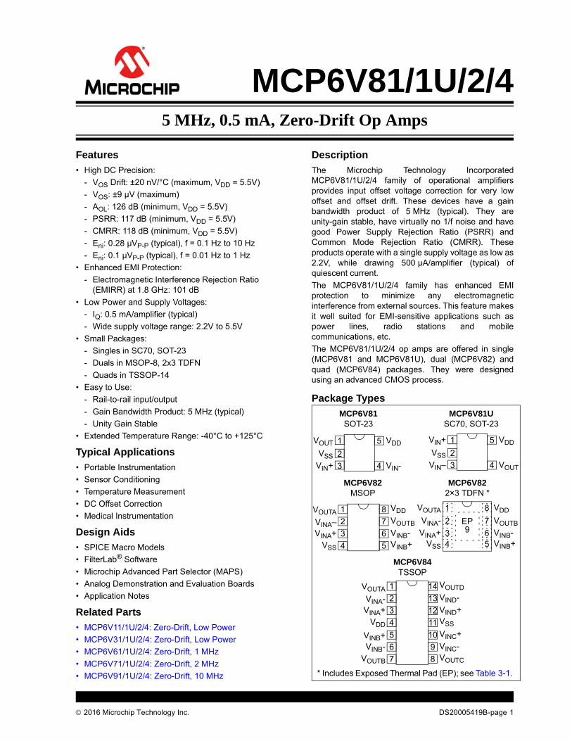
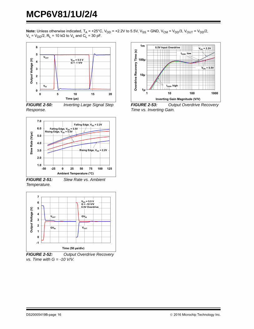
2016 Microchip Technology Inc. DS20005419B-page 1 MCP6V81/1U/2/4 Features • High DC Precision: -V OS Drift: ±20 nV/°C (maximum, V DD = 5.5V) -V OS : ±9 μV (maximum) -A OL : 126 dB (minimum, V DD = 5.5V) - PSRR: 117 dB (minimum, V DD = 5.5V) - CMRR: 118 dB (minimum, V DD = 5.5V) -E ni : 0.28 μV P-P (typical), f = 0.1 Hz to 10 Hz -E ni : 0.1 μV P-P (typical), f = 0.01 Hz to 1 Hz • Enhanced EMI Protection: - Electromagnetic Interference Rejection Ratio (EMIRR) at 1.8 GHz: 101 dB • Low Power and Supply Voltages: -I Q : 0.5 mA/amplifier (typical) - Wide supply voltage range: 2.2V to 5.5V • Small Packages: - Singles in SC70, SOT-23 - Duals in MSOP-8, 2x3 TDFN - Quads in TSSOP-14 • Easy to Use: - Rail-to-rail input/output - Gain Bandwidth Product: 5 MHz (typical) - Unity Gain Stable • Extended Temperature Range: -40°C to +125°C Typical Applications • Portable Instrumentation • Sensor Conditioning • Temperature Measurement • DC Offset Correction • Medical Instrumentation Design Aids • SPICE Macro Models • FilterLab ® Software • Microchip Advanced Part Selector (MAPS) • Analog Demonstration and Evaluation Boards • Application Notes Related Parts • MCP6V11/1U/2/4: Zero-Drift, Low Power • MCP6V31/1U/2/4: Zero-Drift, Low Power • MCP6V61/1U/2/4: Zero-Drift, 1 MHz • MCP6V71/1U/2/4: Zero-Drift, 2 MHz • MCP6V91/1U/2/4: Zero-Drift, 10 MHz Description The Microchip Technology Incorporated MCP6V81/1U/2/4 family of operational amplifiers provides input offset voltage correction for very low offset and offset drift. These devices have a gain bandwidth product of 5 MHz (typical). They are unity-gain stable, have virtually no 1/f noise and have good Power Supply Rejection Ratio (PSRR) and Common Mode Rejection Ratio (CMRR). These products operate with a single supply voltage as low as 2.2V, while drawing 500 μA/amplifier (typical) of quiescent current. The MCP6V81/1U/2/4 family has enhanced EMI protection to minimize any electromagnetic interference from external sources. This feature makes it well suited for EMI-sensitive applications such as power lines, radio stations and mobile communications, etc. The MCP6V81/1U/2/4 op amps are offered in single (MCP6V81 and MCP6V81U), dual (MCP6V82) and quad (MCP6V84) packages. They were designed using an advanced CMOS process. Package Types V IN + V SS V IN - 1 2 3 5 4 V DD V OUT MCP6V81 SOT-23 MCP6V81U SC70, SOT-23 V IN – V SS V OUT 1 2 3 5 4 V DD V IN + V INA + V INA – V SS 1 2 3 4 8 7 6 5 V OUTA V DD V OUTB V INB - V INB + MCP6V82 MSOP MCP6V82 2×3 TDFN * V INA + V INA - V SS V OUTB V INB - 1 2 3 4 8 7 6 5 V INB + V DD V OUTA EP 9 V INA + V INA - V DD 1 2 3 4 14 13 12 11 V OUTA V OUTD V IND - V IND + V SS MCP6V84 TSSOP V INB - V INB + V OUTB 5 6 7 10 9 8 V INC + V INC - V OUTC * Includes Exposed Thermal Pad (EP); see Table 3-1. 5 MHz, 0.5 mA, Zero-Drift Op Amps
Transcript
MCP6V81/1U/2/45 MHz, 0.5 mA, Zero-Drift Op Amps
Features
• High DC Precision:
- VOS Drift: ±20 nV/°C (maximum, VDD = 5.5V)
- VOS: ±9 µV (maximum)
- AOL: 126 dB (minimum, VDD = 5.5V)
- PSRR: 117 dB (minimum, VDD = 5.5V)
- CMRR: 118 dB (minimum, VDD = 5.5V)
- Eni: 0.28 µVP-P (typical), f = 0.1 Hz to 10 Hz
- Eni: 0.1 µVP-P (typical), f = 0.01 Hz to 1 Hz
• Enhanced EMI Protection:
- Electromagnetic Interference Rejection Ratio (EMIRR) at 1.8 GHz: 101 dB
• Low Power and Supply Voltages:
- IQ: 0.5 mA/amplifier (typical)
- Wide supply voltage range: 2.2V to 5.5V
• Small Packages:
- Singles in SC70, SOT-23
- Duals in MSOP-8, 2x3 TDFN
- Quads in TSSOP-14
• Easy to Use:
- Rail-to-rail input/output
- Gain Bandwidth Product: 5 MHz (typical)
- Unity Gain Stable
• Extended Temperature Range: -40°C to +125°C
Typical Applications
• Portable Instrumentation
• Sensor Conditioning
• Temperature Measurement
• DC Offset Correction
• Medical Instrumentation
Design Aids
• SPICE Macro Models
• FilterLab® Software
• Microchip Advanced Part Selector (MAPS)
• Analog Demonstration and Evaluation Boards
• Application Notes
Related Parts
• MCP6V11/1U/2/4: Zero-Drift, Low Power
• MCP6V31/1U/2/4: Zero-Drift, Low Power
• MCP6V61/1U/2/4: Zero-Drift, 1 MHz
• MCP6V71/1U/2/4: Zero-Drift, 2 MHz
• MCP6V91/1U/2/4: Zero-Drift, 10 MHz
Description
The Microchip Technology IncorporatedMCP6V81/1U/2/4 family of operational amplifiersprovides input offset voltage correction for very lowoffset and offset drift. These devices have a gainbandwidth product of 5 MHz (typical). They areunity-gain stable, have virtually no 1/f noise and havegood Power Supply Rejection Ratio (PSRR) andCommon Mode Rejection Ratio (CMRR). Theseproducts operate with a single supply voltage as low as2.2V, while drawing 500 µA/amplifier (typical) ofquiescent current.
The MCP6V81/1U/2/4 family has enhanced EMIprotection to minimize any electromagneticinterference from external sources. This feature makesit well suited for EMI-sensitive applications such aspower lines, radio stations and mobilecommunications, etc.
The MCP6V81/1U/2/4 op amps are offered in single(MCP6V81 and MCP6V81U), dual (MCP6V82) andquad (MCP6V84) packages. They were designedusing an advanced CMOS process.
Package Types
VIN+
VSS
VIN-
1
2
3
5
4
VDDVOUT
MCP6V81SOT-23
MCP6V81USC70, SOT-23
VIN–
VSS
VOUT
1
2
3
5
4
VDDVIN+
VINA+VINA–
VSS
1
2
3
4
8
7
6
5
VOUTA VDD
VOUTB
VINB-VINB+
MCP6V82MSOP
MCP6V822×3 TDFN *
VINA+
VINA-
VSS
VOUTB
VINB-
1
2
34
8
7
65 VINB+
VDDVOUTA
EP9
VINA+VINA-
VDD
1
2
3
4
14
13
12
11
VOUTA VOUTD
VIND-
VIND+VSS
MCP6V84TSSOP
VINB-VINB+
VOUTB
5
6
7
10
9
8
VINC+
VINC-VOUTC
* Includes Exposed Thermal Pad (EP); see Table 3-1.
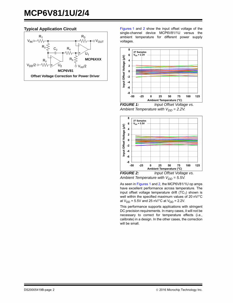
Typical Application Circuit Figures 1 and 2 show the input offset voltage of thesingle-channel device MCP6V81/1U versus theambient temperature for different power supplyvoltages.
FIGURE 1: Input Offset Voltage vs. Ambient Temperature with VDD = 2.2V.
FIGURE 2: Input Offset Voltage vs. Ambient Temperature with VDD = 5.5V.
As seen in Figures 1 and 2, the MCP6V81/1U op ampshave excellent performance across temperature. Theinput offset voltage temperature drift (TC1) shown iswell within the specified maximum values of 20 nV/°Cat VDD = 5.5V and 25 nV/°C at VDD = 2.2V.
This performance supports applications with stringentDC precision requirements. In many cases, it will not benecessary to correct for temperature effects (i.e.,calibrate) in a design. In the other cases, the correctionwill be small.
Current at Input Pins ..............................................................................................................................................±2 mA
Analog Inputs (VIN+ and VIN-)(1) ...............................................................................................VSS – 1.0V to VDD + 1.0V
All Other Inputs and Outputs ....................................................................................................VSS – 0.3V to VDD + 0.3V
Difference Input Voltage .................................................................................................................................|VDD – VSS|
Output Short Circuit Current ........................................................................................................................... Continuous
Current at Output and Supply Pins ......................................................................................................................±30 mA
Storage Temperature ............................................................................................................................. -65°C to +150°C
Maximum Junction Temperature .......................................................................................................................... +150°C
ESD protection on all pins (HBM, CDM, MM)
MCP6V81/1U 4 kV, 1.5 kV, 400V
MCP6V82/4 4 kV, 1.5 kV, 300V
Note 1: See Section 4.2.1 “Rail-to-Rail Inputs”.
1.2 Specifications
† Notice: Stresses above those listed under “Absolute Maximum Ratings” may cause permanent damage to thedevice. This is a stress rating only and functional operation of the device at those or any other conditions above thoseindicated in the operational listings of this specification is not implied. Exposure to maximum rating conditions forextended periods may affect device reliability.
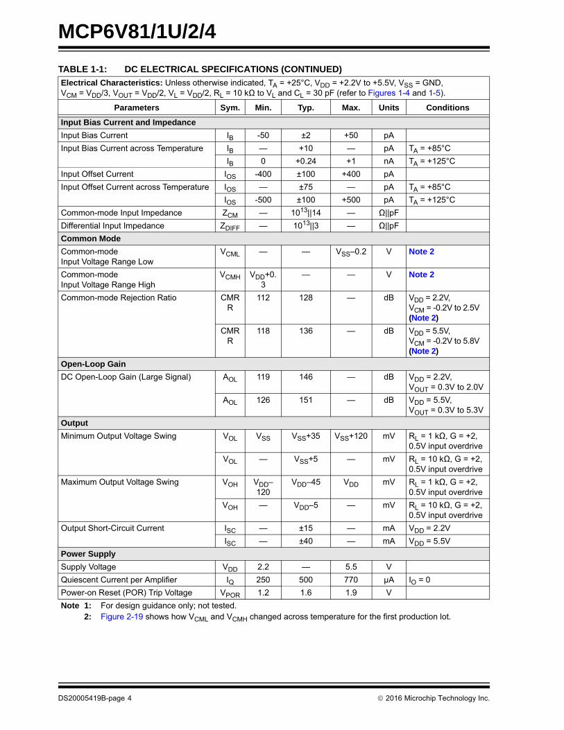
TABLE 1-1: DC ELECTRICAL SPECIFICATIONS
Electrical Characteristics: Unless otherwise indicated, TA = +25°C, VDD = +2.2V to +5.5V, VSS = GND, VCM = VDD/3, VOUT = VDD/2, VL = VDD/2, RL = 10 kΩ to VL and CL = 30 pF (refer to Figures 1-4 and 1-5).
Parameters Sym. Min. Typ. Max. Units Conditions
Input Offset
Input Offset Voltage VOS -9 — +9 µV TA = +25°C
Input Offset Voltage Drift with Temperature(Linear Temperature Coefficient)
TC1
-25 — +25 nV/°C TA = -40 to +125°C,VDD = 2.2V (Note 1)
-20 — +20 nV/°C TA = -40 to +125°C,VDD = 5.5V (Note 1)
Input Offset Voltage Quadratic Temperature Coefficient
TC2
— ±30 — pV/°C2 TA = -40 to +125°CVDD = 2.2V
— ±20 — pV/°C2 TA = -40 to +125°CVDD = 5.5V
Input Offset Voltage Aging ∆VOS — ±0.25 — µV 408 hours Life Test at +150°,measured at +25°C.
Power Supply Rejection Ratio PSRR 117 127 — dB
Note 1: For design guidance only; not tested.2: Figure 2-19 shows how VCML and VCMH changed across temperature for the first production lot.
2016 Microchip Technology Inc. DS20005419B-page 3
MCP6V81/1U/2/4
Input Bias Current and Impedance
Input Bias Current IB -50 ±2 +50 pA
Input Bias Current across Temperature IB — +10 — pA TA = +85°C
IB 0 +0.24 +1 nA TA = +125°C
Input Offset Current IOS -400 ±100 +400 pA
Input Offset Current across Temperature IOS — ±75 — pA TA = +85°C
Output Short-Circuit Current ISC — ±15 — mA VDD = 2.2V
ISC — ±40 — mA VDD = 5.5V
Power Supply
Supply Voltage VDD 2.2 — 5.5 V
Quiescent Current per Amplifier IQ 250 500 770 µA IO = 0
Power-on Reset (POR) Trip Voltage VPOR 1.2 1.6 1.9 V
TABLE 1-1: DC ELECTRICAL SPECIFICATIONS (CONTINUED)
Electrical Characteristics: Unless otherwise indicated, TA = +25°C, VDD = +2.2V to +5.5V, VSS = GND, VCM = VDD/3, VOUT = VDD/2, VL = VDD/2, RL = 10 kΩ to VL and CL = 30 pF (refer to Figures 1-4 and 1-5).
Parameters Sym. Min. Typ. Max. Units Conditions
Note 1: For design guidance only; not tested.2: Figure 2-19 shows how VCML and VCMH changed across temperature for the first production lot.
DS20005419B-page 4 2016 Microchip Technology Inc.
MCP6V81/1U/2/4
TABLE 1-2: AC ELECTRICAL SPECIFICATIONS
Electrical Characteristics: Unless otherwise indicated, TA = +25°C, VDD = +2.2V to +5.5V, VSS = GND, VCM = VDD/3, VOUT = VDD/2, VL = VDD/2, RL = 10 kΩ to VL and CL = 30 pF (refer to Figures 1-4 and 1-5).
Parameters Sym. Min. Typ. Max. Units Conditions
Amplifier AC Response
Gain Bandwidth Product GBWP — 5 — MHz
Slew Rate SR — 4 — V/µs
Phase Margin PM — 60 — °C G = +1
Amplifier Noise Response
Input Noise Voltage Eni — 0.1 — µVP-P f = 0.01 Hz to 1 Hz
Eni — 0.28 — µVP-P f = 0.1 Hz to 10 Hz
Input Noise Voltage Density eni — 13 — nV/√Hz f < 2 kHz
Input Noise Current Density ini — 6 — fA/√Hz
Amplifier Distortion(1)
Intermodulation Distortion (AC) IMD — 100 — µVPK VCM tone = 100 mVPK at 1 kHz,GN = 11, RTI
Amplifier Step Response
Start-Up Time tSTR — 100 — µs G = +1, 0.1% VOUT settling (Note 2)
Offset Correction Settling Time tSTL — 30 — µs G = +1, VIN step of 2V,VOS within 100 µV of its final value
Output Overdrive Recovery Time tODR — 60 — µs G = -10, ±0.5V input overdrive to VDD/2,VIN 50% point to VOUT 90% point (Note 3)
EMI Protection
EMI Rejection Ratio EMIRR — 90 — dB VIN = 0.1 VPK, f = 400 MHz
— 100 — VIN = 0.1 VPK, f = 900 MHz
— 101 — VIN = 0.1 VPK, f = 1800 MHz
— 105 — VIN = 0.1 VPK, f = 2400 MHz
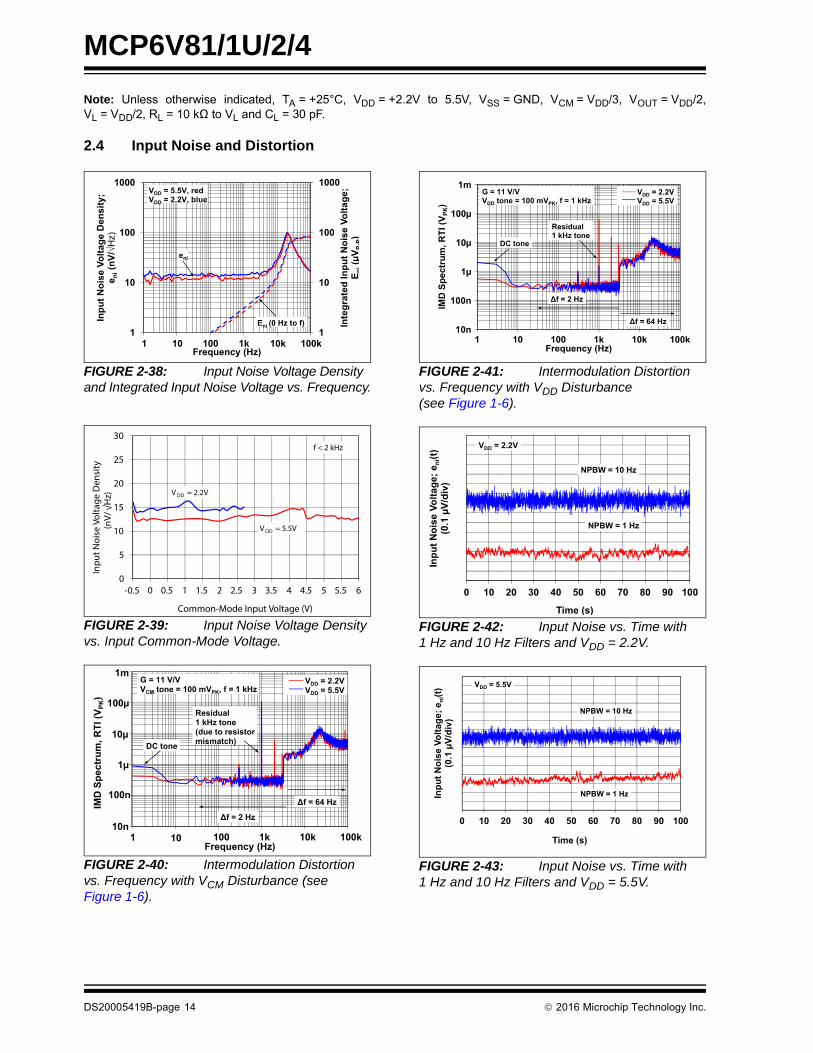
Note 1: These parameters were characterized using the circuit in Figure 1-6. In Figures 2-40 and 2-41, there is an IMD tone at DC, a residual tone at 1 kHz and other IMD tones and clock tones. IMD is Referred to Input (RTI).
2: High gains behave differently; see Section 4.3.3 “Offset at Power-Up”.3: tSTL and tODR include some uncertainty due to clock edge timing.
TABLE 1-3: TEMPERATURE SPECIFICATIONS
Electrical Characteristics: Unless otherwise indicated, all limits are specified for: VDD = +2.2V to +5.5V, VSS = GND.
Parameters Sym. Min. Typ. Max. Units Conditions
Temperature Ranges
Specified Temperature Range TA -40 — +125 °C
Operating Temperature Range TA -40 — +125 °C Note 1
Storage Temperature Range TA -65 — +150 °C
Thermal Package Resistances
Thermal Resistance, 5LD-SC70 JA — 209 — °C/W
Thermal Resistance, 5LD-SOT-23 JA — 201 — °C/W
Thermal Resistance, 8L-2x3 TDFN JA — 53 — °C/W
Thermal Resistance, 8L-MSOP JA — 211 — °C/W
Thermal Resistance, 14L-TSSOP JA — 100 — °C/W
Note 1: Operation must not cause TJ to exceed Maximum Junction Temperature specification (+150°C).
2016 Microchip Technology Inc. DS20005419B-page 5
MCP6V81/1U/2/4
1.3 Timing Diagrams
FIGURE 1-1: Amplifier Start-Up.
FIGURE 1-2: Offset Correction Settling Time.
FIGURE 1-3: Output Overdrive Recovery.
1.4 Test Circuits
The circuits used for most DC and AC tests are shownin Figures 1-4 and 1-5. Lay the bypass capacitors outas discussed in Section 4.3.10 “Supply Bypassingand Filtering”. RN is equal to the parallel combinationof RF and RG to minimize bias current effects.
FIGURE 1-4: AC and DC Test Circuit for Most Non-Inverting Gain Conditions.
FIGURE 1-5: AC and DC Test Circuit for Most Inverting Gain Conditions.
The circuit in Figure 1-6 tests the input’s dynamicbehavior (i.e., IMD, tSTR, tSTL and tODR). Thepotentiometer balances the resistor network (VOUTshould equal VREF at DC). The op amp’s common-modeinput voltage is VCM = VIN/2. The error at the input(VERR) appears at VOUT with a noise gain of 10 V/V.
FIGURE 1-6: Test Circuit for Dynamic Input Behavior.
VDD
VOUT
1.001(VDD/3)
0.999(VDD/3)
tSTR
0V2.2V to 5.5V2.2V
VIN
VOS
VOS + 100 µV
VOS – 100 µV
tSTL
VIN
VOUT
VDD
VSS
tODR
tODR
VDD/2
VDD
RG RF
RNVOUT
VIN
VDD/3
1 µF
CL RL
VL
100 nF
RISO
MCP6V8X+
-
VDD
RG RF
RNVOUT
VDD/3
VIN
1 µF
CL RL
VL
100 nF
RISO
MCP6V8X+
-
VDD
VOUT
1 µF
CL
VL
RISO
11.0 kΩ 249Ω
11.0 kΩ 500Ω
VIN
VREF = VDD/3
0.1%
0.1% 25 turn
100 kΩ
100 kΩ
0.1%
0.1%
RL
0 Ω
30 pF open
100 nF
1%
MCP6V8X
DS20005419B-page 6 2016 Microchip Technology Inc.
MCP6V81/1U/2/4
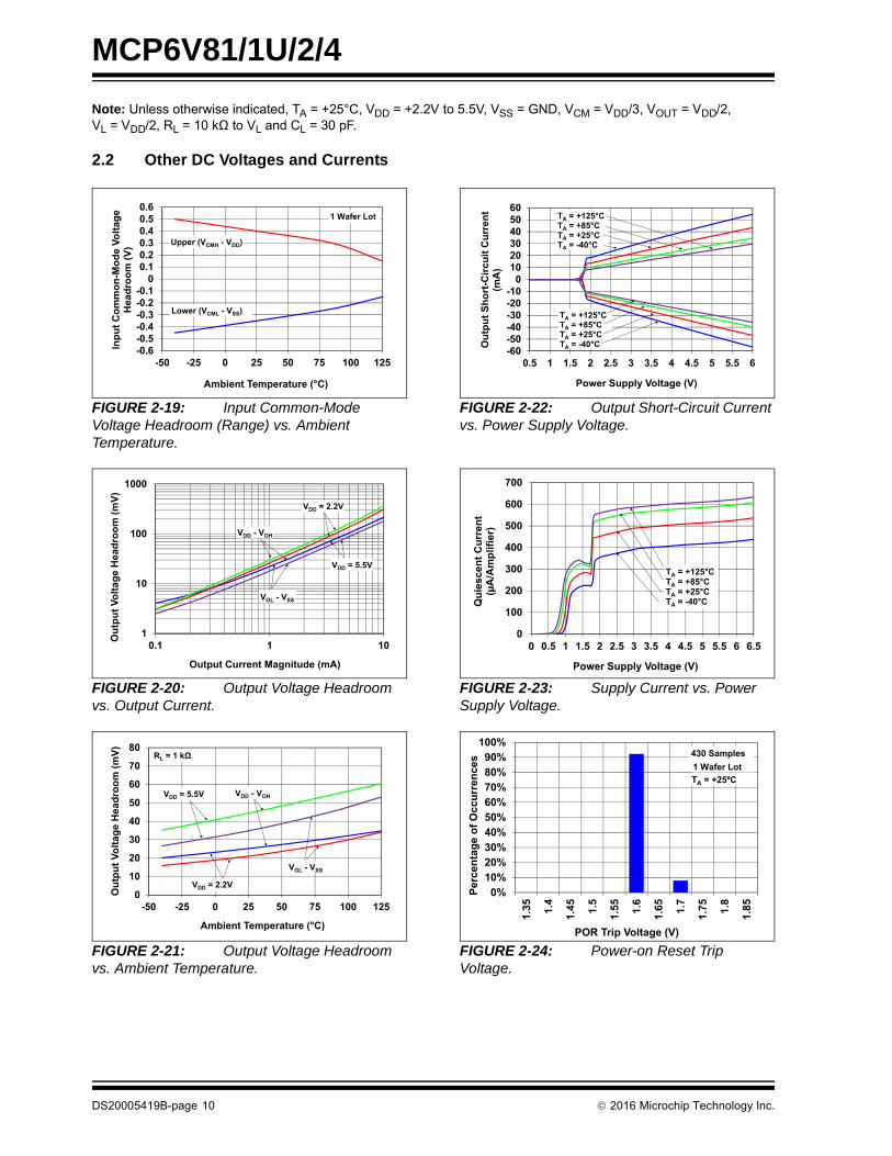
2.0 TYPICAL PERFORMANCE CURVES
Note: Unless otherwise indicated, TA = +25°C, VDD = +2.2V to 5.5V, VSS = GND, VCM = VDD/3, VOUT = VDD/2, VL = VDD/2, RL = 10 kΩ to VL and CL = 30 pF.
2.1 DC Input Precision
FIGURE 2-1: Input Offset Voltage.
FIGURE 2-2: Input Offset Voltage Drift.
FIGURE 2-3: Input Offset Voltage Quadratic Temperature Coefficient.
FIGURE 2-4: Input Offset Voltage vs. Power Supply Voltage with VCM = VCML.
FIGURE 2-5: Input Offset Voltage vs. Power Supply Voltage with VCM = VCMH.
FIGURE 2-6: Input Offset Voltage vs. Output Voltage with VDD = 2.2V.
Note: The graphs and tables provided following this note are a statistical summary based on a limited number ofsamples and are provided for informational purposes only. The performance characteristics listed hereinare not tested or guaranteed. In some graphs or tables, the data presented may be outside the specifiedoperating range (e.g., outside specified power supply range) and therefore outside the warranted range.
The non-inverting and inverting inputs arehigh-impedance CMOS inputs with low bias currents.
3.3 Power Supply Pins (VDD, VSS)
The positive power supply (VDD) is 2.2V to 5.5V higherthan the negative power supply (VSS). For normaloperation, the other pins are between VSS and VDD.
Typically, these parts are used in a single (positive)supply configuration. In this case, VSS is connected toground and VDD is connected to the supply. VDD willneed bypass capacitors.
3.4 Exposed Thermal Pad (EP)
There is an internal connection between the exposedthermal pad (EP) and the VSS pin; they must beconnected to the same potential on the printed circuitboard (PCB).
This pad can be connected to a PCB ground plane toprovide a larger heat sink. This improves the packagethermal resistance (θJA).
TABLE 3-1: PIN FUNCTION TABLE
MCP6V81 MCP6V81U MCP6V82 MCP6V84
Symbol DescriptionSOT-23
SOT-23,SC70
2X3 TDFN MSOP TSSOP
1 4 1 1 1 VOUT Output
4 3 2 2 2 VIN- Inverting Input
3 1 3 3 3 VIN+ Non-Inverting Input
5 5 8 8 4 VDD Positive Power Supply
— — 5 5 5 VINB+ Non-inverting Input (Op Amp B)
— — 6 6 6 VINB- Inverting Input (Op Amp B)
— — 7 7 7 VOUTB Output (Op Amp B)
— — — — 8 VOUTC Output (Op Amp C)
— — — — 9 VINC- Inverting Input (Op Amp C)
— — — — 10 VINC+ Non-inverting Input (Op Amp C)
2 2 4 4 11 VSS Negative Power Supply
— — — — 12 VIND+ Non-inverting Input (Op Amp D)
— — — — 13 VIND- Inverting Input (Op Amp D)
— — — — 14 VOUTD Output (Op Amp D)
— — 9 — — EP Exposed Thermal Pad (EP); must be connected to VSS
2016 Microchip Technology Inc. DS20005419B-page 17
MCP6V81/1U/2/4
NOTES:
DS20005419B-page 18 2016 Microchip Technology Inc.
MCP6V81/1U/2/4
4.0 APPLICATIONS
The MCP6V81/1U/2/4 family of zero-drift op amps ismanufactured using Microchip’s state-of-the-art CMOSprocess. It is designed for precision applications withrequirements for small packages and low power. Its lowsupply voltage and low quiescent current make theMCP6V81/1U/2/4 devices ideal for battery-poweredapplications.
4.1 Overview of Zero-Drift Operation
Figure 4-1 shows a simplified diagram of theMCP6V81/1U/2/4 zero-drift op amp. This diagram willbe used to explain how slow voltage errors are reducedin this architecture (much better VOS, VOS/TA (TC1),CMRR, PSRR, AOL and 1/f noise).
FIGURE 4-1: Simplified Zero-Drift Op Amp Functional Diagram.
4.1.1 BUILDING BLOCKS
The main amplifier is designed for high gain andbandwidth, with a differential topology. Its main inputpair (+ and - pins at the top left) is used for the higherfrequency portion of the input signal. Its auxiliary inputpair (+ and - pins at the bottom left) is used for thelow-frequency portion of the input signal and correctsthe op amp’s input offset voltage. Both inputs areadded together internally.
The auxiliary amplifier, chopper input switches andchopper output switches provide a high DC gain to theinput signal. DC errors are modulated to higherfrequencies, while white noise is modulated to a lowfrequency.
The low-pass filter reduces high-frequency content,including harmonics of the chopping clock.
The output buffer drives external loads at the VOUT pin(VREF is an internal reference voltage).
The oscillator runs at fOSC1 = 200 kHz. Its output isdivided by two, to produce the chopping clock rate offCHOP = 100 kHz.
The internal Power-on Reset (POR) starts the part in aknown good state, protecting against power supplybrown-outs.
The digital control block controls switching and PORevents.
4.1.2 CHOPPING ACTION
Figure 4-2 shows the amplifier connections for the firstphase of the chopping clock and Figure 4-3 shows theconnections for the second phase. Its slow voltage errorsalternate in polarity, making the average error small.
FIGURE 4-2: First Chopping Clock Phase; Equivalent Amplifier Diagram.
FIGURE 4-3: Second Chopping Clock Phase; Equivalent Amplifier Diagram.
VIN+
VIN– Main
BufferVOUT
VREF
Amp.
Output
NC
Aux.Amp.
ChopperInput
Switches
ChopperOutput
Switches
Oscillator
Low-PassFilter
PORDigital Control
+
-
+-
+-
+-
+-
+-
VIN+
VIN– MainAmp. NC
Aux.Amp.
Low-PassFilter
+-
+-
+-
+-
+-
VIN+
VIN– MainAmp. NC
Aux.Amp.
Low-PassFilter
+-
+-
+-
+-
+-
2016 Microchip Technology Inc. DS20005419B-page 19
MCP6V81/1U/2/4
4.1.3 INTERMODULATION DISTORTION (IMD)
These op amps will show intermodulation distortion(IMD) products when an AC signal is present.
The signal and clock can be decomposed into sinewave tones (Fourier series components). These tonesinteract with the zero-drift circuitry’s nonlinear responseto produce IMD tones at sum and differencefrequencies. Each of the square wave clock’sharmonics has a series of IMD tones centered on it(see Figures 2-40 and 2-41).
4.2 Other Functional Blocks
4.2.1 RAIL-TO-RAIL INPUTS
The input stage of the MCP6V81/1U/2/4 op amps usestwo differential CMOS input stages in parallel. Oneoperates at low common-mode input voltage (VCM,which is approximately equal to VIN+ and VIN- in normaloperation), and the other operates at high VCM. Withthis topology, the input operates with VCM up toVDD + 0.3V and down to VSS – 0.2V, at +25°C (seeFigure 2-19). The input offset voltage (VOS) ismeasured at VCM = VSS – 0.2V and VDD + 0.3V toensure proper operation.
4.2.1.1 Phase Reversal
The input devices are designed to not exhibit phaseinversion when the input pins exceed the supplyvoltages. Figure 2-46 shows an input voltageexceeding both supplies with no phase inversion.
4.2.1.2 Input Voltage Limits
In order to prevent damage and/or improper operationof these amplifiers, the circuit must limit the voltages atthe input pins (see Section 1.1 “Absolute MaximumRatings †”). This requirement is independent of theinput current limits discussed later on.
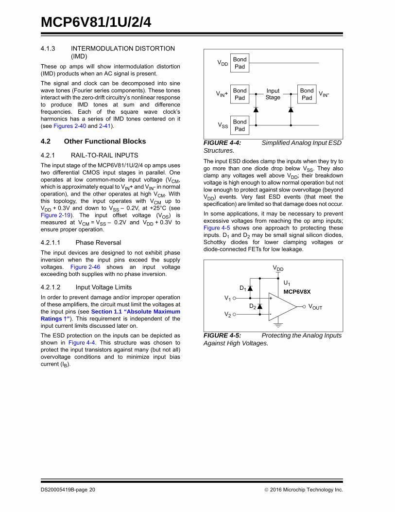
The ESD protection on the inputs can be depicted asshown in Figure 4-4. This structure was chosen toprotect the input transistors against many (but not all)overvoltage conditions and to minimize input biascurrent (IB).
FIGURE 4-4: Simplified Analog Input ESD Structures.
The input ESD diodes clamp the inputs when they try togo more than one diode drop below VSS. They alsoclamp any voltages well above VDD; their breakdownvoltage is high enough to allow normal operation but notlow enough to protect against slow overvoltage (beyondVDD) events. Very fast ESD events (that meet thespecification) are limited so that damage does not occur.
In some applications, it may be necessary to preventexcessive voltages from reaching the op amp inputs;Figure 4-5 shows one approach to protecting theseinputs. D1 and D2 may be small signal silicon diodes,Schottky diodes for lower clamping voltages ordiode-connected FETs for low leakage.
FIGURE 4-5: Protecting the Analog Inputs Against High Voltages.
BondPad
BondPad
BondPad
VDD
VIN+
VSS
InputStage
BondPad
VIN-
V1
VDD
D1
VOUTV2
D2
U1
MCP6V8X+
-
DS20005419B-page 20 2016 Microchip Technology Inc.
MCP6V81/1U/2/4
4.2.1.3 Input Current Limits
In order to prevent damage and/or improper operationof these amplifiers, the circuit must limit the currentsinto the input pins (see Section 1.1 “AbsoluteMaximum Ratings †”). This requirement isindependent of the voltage limits discussed previously.
Figure 4-6 shows one approach to protecting theseinputs. The R1 and R2 resistors limit the possiblecurrent in or out of the input pins (and into D1 and D2).The diode currents will dump onto VDD.
FIGURE 4-6: Protecting the Analog Inputs Against High Currents.
It is also possible to connect the diodes to the left of theR1 and R2 resistors. In this case, the currents throughthe D1 and D2 diodes need to be limited by some othermechanism. The resistors then serve as in-rush currentlimiters; the DC current into the input pins (VIN+ andVIN-) should be very small.
A significant amount of current can flow out of theinputs (through the ESD diodes) when the common-mode input voltage (VCM) is below ground (VSS) (seeFigure 2-18).
4.2.2 RAIL-TO-RAIL OUTPUT
The output voltage range of the MCP6V81/1U/2/4zero-drift op amps is VDD – 5 mV (typical) andVSS + 5 mV (typical) when RL = 10 kΩ is connected toVDD/2 and VDD = 5.5V. Refer to Figures 2-20 and 2-21for more information.
This op amp is designed to drive light loads; useanother amplifier to buffer the output from heavy loads.
4.3 Application Tips
4.3.1 INPUT OFFSET VOLTAGE OVER TEMPERATURE
Table 1-1 gives both the linear and quadratictemperature coefficients (TC1 and TC2) of input offsetvoltage. The input offset voltage, at any temperature inthe specified range, can be calculated as follows:
EQUATION 4-1:
4.3.2 DC GAIN PLOTS
Figures 2-10 to 2-12 are histograms of the reciprocals(in units of µV/V) of CMRR, PSRR and AOL,respectively. They represent the change in input offsetvoltage (VOS) with a change in common-mode inputvoltage (VCM), power supply voltage (VDD) and outputvoltage (VOUT). The histograms are based on datataken with the production test equipment and theresults reflect the trade-off between accuracy and testtime. The actual performance of the devices is typicallyhigher than shown in Figures 2-10 to 2-12.
The 1/AOL histogram is centered near 0 µV/V becausethe measurements are dominated by the op amp’sinput noise. The negative values shown representnoise and tester limitations, not unstable behavior.Production tests make multiple VOS measurements,which validates an op amp's stability; an unstable partwould show greater VOS variability or the output wouldstick at one of the supply rails.
4.3.3 OFFSET AT POWER-UP
When these parts power up, the input offset (VOS) startsat its uncorrected value (usually less than ±5 mV).Circuits with high DC gain can cause the output to reachone of the two rails. In this case, the time to a validoutput is delayed by an output overdrive time (like tODR)in addition to the start-up time (like tSTR).
It can be simple to avoid this extra start-up time.Reducing the gain is one method. Adding a capacitoracross the feedback resistor (RF) is another method.
V1R1
VDD
D1
min(R1, R2) >VSS – min(V1, V2)
2 mA
VOUTV2
R2
D2
min(R1, R2) >max(V1, V2) – VDD
2 mA
U1
MCP6V8X+
-
VOS TA VOS TC1T TC2T2
+ +=
Where:
T = TA – 25°C
VOS(TA) = Input offset voltage at TA
VOS = Input offset voltage at +25°C
TC1 = Linear temperature coefficient
TC2 = Quadratic temperature coefficient
2016 Microchip Technology Inc. DS20005419B-page 21
MCP6V81/1U/2/4
4.3.4 SOURCE RESISTANCES
The input bias currents have two significantcomponents: switching glitches that dominate at roomtemperature and below, and input ESD diode leakagecurrents that dominate at +85°C and above.
Make the resistances seen by the inputs small andequal. This minimizes the output offset caused by theinput bias currents.
The inputs should see a resistance on the order of 10Ωto 1 kΩ at high frequencies (i.e., above 1 MHz). Thishelps minimize the impact of switching glitches, whichare very fast, on overall performance. In some cases, itmay be necessary to add resistors in series with theinputs to achieve this improvement in performance.
Small input resistances may be needed for high gains.Without them, parasitic capacitances might causepositive feedback and instability.
4.3.5 SOURCE CAPACITANCE
The capacitances seen by the two inputs should besmall. Large input capacitances and sourceresistances, together with high gain, can lead topositive feedback and instability.
4.3.6 CAPACITIVE LOADS
Driving large capacitive loads can cause stabilityproblems for voltage feedback op amps. As the loadcapacitance increases, the feedback loop’s phasemargin decreases and the closed-loop bandwidth isreduced. This produces gain peaking in the frequencyresponse, with overshoot and ringing in the stepresponse. These zero-drift op amps have a differentoutput impedance than most op amps, due to theirunique topology.
When driving a capacitive load with these op amps, aseries resistor at the output (RISO in Figure 4-7)improves the feedback loop’s phase margin (stability)by making the output load resistive at higherfrequencies. The bandwidth will be generally lowerthan the bandwidth with no capacitive load.
Figure 4-8 gives recommended RISO values for differentcapacitive loads and gains. The x-axis is the loadcapacitance (CL). The y-axis is the resistance (RISO).
GN is the circuit’s noise gain. For non-inverting gains,GN and the Signal Gain are equal. For inverting gains,GN is 1+|Signal Gain| (e.g., -1 V/V gives GN = +2 V/V).
FIGURE 4-8: Recommended RISO values for Capacitive Loads.
After selecting RISO for your circuit, double check theresulting frequency response peaking and stepresponse overshoot. Modify the RISO value until theresponse is reasonable. Bench evaluation is helpful.
4.3.7 STABILIZING OUTPUT LOADS
This family of zero-drift op amps has an outputimpedance that has a double zero when the gain is low(see Figures 2-32 and 2-33). This can cause a largephase shift in feedback networks that have low-impedance near the part’s bandwidth. This large phaseshift can cause stability problems.
Figure 4-9 shows that the load on the output is(RL + RISO)||(RF + RG), where RISO is before the load(like Figure 4-7). This load needs to be large enough tomaintain stability; it should be at least 10 kΩ.
FIGURE 4-9: Output Load.
RISO
CL
VOUT
U1
MCP6V81
-
+
1
10
100
1000
10000
Rec
omm
ende
d R
ISO
(Ω)
Normalized Load Capacitance; CL/√√GN (F)
GN:1 V/V10 V/V100 V/V
VDD = 5.5 V RL = 10 k
1p 10p 100p 1n 10n 100n 1µ
RG RFVOUT
U1
MCP6V81
RL CL-
+
RISO
DS20005419B-page 22 2016 Microchip Technology Inc.
MCP6V81/1U/2/4
4.3.8 GAIN PEAKING
Figure 4-10 shows an op amp circuit that representsnon-inverting amplifiers (VM is a DC voltage and VP isthe input) or inverting amplifiers (VP is a DC voltageand VM is the input). The CN and CG capacitancesrepresent the total capacitance at the input pins; theyinclude the op amp’s common-mode input capacitance(CCM), board parasitic capacitance and any capacitorplaced in parallel. The CFP capacitance represents theparasitic capacitance coupling the output andnon-inverting input pins.
FIGURE 4-10: Amplifier with Parasitic Capacitance.
CG acts in parallel with RG (except for a gain of +1 V/V),which causes an increase in gain at high frequencies.CG also reduces the phase margin of the feedbackloop, which becomes less stable. This effect can bereduced by reducing either CG or RF||RG.
CN and RN form a low-pass filter that affects the signalat VP. This filter has a single real pole at 1/(2πRNCN).
The largest value of RF that should be used dependson noise gain (see GN in Section 4.3.6 “CapacitiveLoads”), CG and the open-loop gain’s phase shift. Anapproximate limit for RF is:
EQUATION 4-2:
Some applications may modify these values to reduceeither output loading or gain peaking (step-responseovershoot).
At high gains, RN needs to be small in order to preventpositive feedback and oscillations. Large CN valuescan also help.
4.3.9 REDUCING UNDESIRED NOISE AND SIGNALS
Reduce undesired noise and signals with:
• Low-bandwidth signal filters:
- Minimize random analog noise
- Reduce interfering signals
• Good PCB layout techniques:
- Minimize crosstalk
- Minimize parasitic capacitances and inductances that interact with fast-switching edges
• Good power supply design:
- Isolation from other parts
- Filtering of interference on supply line(s)
4.3.10 SUPPLY BYPASSING AND FILTERING
With this family of operational amplifiers, the powersupply pin (VDD for single supply) should have a localbypass capacitor (i.e., 0.01 µF to 0.1 µF) within 2 mmof the pin for good high-frequency performance.
These parts also need a bulk capacitor (i.e., 1 µF orlarger) within 100 mm to provide large, slow currents.This bulk capacitor can be shared with other low-noiseanalog parts.
In some cases, high-frequency power supply noise(e.g., switched mode power supplies) may causeundue intermodulation distortion with a DC offset shift;this noise needs to be filtered. Adding a small resistorinto the supply connection can be helpful.
4.3.11 PCB DESIGN FOR DC PRECISION
In order to achieve DC precision on the order of ±1 µV,many physical errors need to be minimized. The designof the printed circuit board (PCB), the wiring and thethermal environment have a strong impact on theprecision achieved. A poor PCB design can easily bemore than 100 times worse than the MCP6V81/1U/2/4op amps’ minimum and maximum specifications.
4.3.11.1 PCB Layout
Any time two dissimilar metals are joined together, atemperature-dependent voltage appears across thejunction (the Seebeck or thermojunction effect). Thiseffect is used in thermocouples to measuretemperature. The following are examples ofthermojunctions on a PCB:
• Components (resistors, op amps, …) soldered to a copper pad
• Wires mechanically attached to the PCB
• Jumpers
• Solder joints
• PCB vias
RG RF
VOUT
U1
MCP6V8X
CG
RNCN
VM
VP
CFP
+
-
RF 10 k 3.5 pFCG
--------------- GN2
2016 Microchip Technology Inc. DS20005419B-page 23
MCP6V81/1U/2/4
Typical thermojunctions have temperature-to-voltageconversion coefficients of 1 to 100 µV/°C (sometimeshigher).
Microchip’s AN1258 “Op Amp Precision Design: PCBLayout Techniques” (DS01258) contains in-depthinformation on PCB layout techniques that minimizethermojunction effects. It also discusses other effects,such as crosstalk, impedances, mechanical stressesand humidity.
4.3.11.2 Crosstalk
DC crosstalk causes offsets that appear as a largerinput offset voltage. Common causes include:
• Common-mode noise (remote sensors)
• Ground loops (current return paths)
• Power supply coupling
Interference from the mains (usually 50 Hz or 60 Hz)and other AC sources can also affect the DCperformance. Nonlinear distortion can convert thesesignals to multiple tones, including a DC shift in voltage.When the signal is sampled by an ADC, these ACsignals can also be aliased to DC, causing an apparentshift in offset.
To reduce interference:
- Keep traces and wires as short as possible
- Use shielding
- Use ground plane (at least a star ground)
- Place the input signal source near the DUT
- Use good PCB layout techniques
- Use a separate power supply filter (bypass capacitors) for these zero-drift op amps
4.3.11.3 Miscellaneous Effects
Keep the resistances seen by the input pins as smalland as near to equal as possible to minimize biascurrent-related offsets.
Make the (trace) capacitances seen by the input pinssmall and equal. This is helpful in minimizing switchingglitch-induced offset voltages.
Bending a coax cable with a radius that is too smallcauses a small voltage drop to appear on the centerconductor (the triboelectric effect). Make sure thebending radius is large enough to keep the conductorsand insulation in full contact.
Mechanical stresses can make some capacitor types(such as some ceramics) output small voltages. Usemore appropriate capacitor types in the signal path andminimize mechanical stresses and vibration.
Humidity can cause electrochemical potential voltagesto appear in a circuit. Proper PCB cleaning helps, asdoes the use of encapsulants.
4.4 Typical Applications
4.4.1 WHEATSTONE BRIDGE
Many sensors are configured as Wheatstone bridges.Strain gauges and pressure sensors are two commonexamples. These signals can be small and thecommon-mode noise large. Amplifier designs with highdifferential gain are desirable.
Figure 4-11 shows how to interface to a Wheatstonebridge with a minimum of components. Because thecircuit is not symmetric, the ADC input is single-endedand there is a minimum of filtering; the CMRR is goodenough for moderate common-mode noise.
FIGURE 4-11: Simple Design.
4.4.2 RTD SENSOR
The ratiometric circuit in Figure 4-12 conditions atwo-wire RTD for applications with a limitedtemperature range. U1 acts as a difference amplifierwith a low-frequency pole. The sensor’s wiringresistance (RW) is corrected in firmware. Failure (open)of the RTD is detected by an out-of-range voltage.
FIGURE 4-12: RTD Sensor.
VDD
R R
R R
100R
0.01C
ADC
VDD
0.2R
0.2R
1 kΩ
U1
MCP6V81+
-
+-
RF
10 nF
ADC
VDD
RN
1.0 µF
VDD
RW
RT
RB
RRTD
RG
100Ω1.00 kΩ
4.99 kΩ
34.8 kΩ
2.00 MΩ10.0 kΩ
U1
MCP6V81
RW
10.0 kΩ
RF2.00 MΩ
10 nF
100 nF
+
-
+-
DS20005419B-page 24 2016 Microchip Technology Inc.
MCP6V81/1U/2/4
4.4.3 OFFSET VOLTAGE CORRECTION
Figure 4-13 shows MCP6V81 (U2) correcting the inputoffset voltage of another op amp (U1). R2 and C2integrate the offset error seen at U1’s input. Theintegration needs to be slow enough to be stable (withthe feedback provided by R1 and R3). R4 and R5attenuate the integrator’s output. This shifts theintegrator pole down in frequency.
FIGURE 4-13: Offset Correction.
4.4.4 PRECISION COMPARATOR
Use high gain before a comparator to improve thelatter’s performance. Do not use MCP6V81/1U/2/4 asa comparator by itself; the VOS correction circuitry doesnot operate properly without a feedback loop.
FIGURE 4-14: Precision Comparator.
U1
MCP6XXX
C2R2
R1 R3
VDD/2
R4
VIN VOUT
R2
VDD/2
R5
U2
MCP6V81
+
-
+
-
VIN
R3R2
VDD/2
VOUT
R5
R4
R1
U1
MCP6V81
U2
MCP6541
+
-
+
-
2016 Microchip Technology Inc. DS20005419B-page 25
MCP6V81/1U/2/4
NOTES:
DS20005419B-page 26 2016 Microchip Technology Inc.
MCP6V81/1U/2/4
5.0 DESIGN AIDS
Microchip provides the basic design aids needed forthe MCP6V81/1U/2/4 family of op amps.
5.1 FilterLab® Software
Microchip’s FilterLab® software is an innovativesoftware tool that simplifies analog active filter (using opamps) design. Available at no cost from the Microchipweb site at www.microchip.com/filterlab, the FilterLabdesign tool provides full schematic diagrams of the filtercircuit with component values. It also outputs the filtercircuit in SPICE format, which can be used with themacro model to simulate actual filter performance.
5.2 Microchip Advanced Part Selector (MAPS)
MAPS is a software tool that helps efficiently identifyMicrochip devices that fit a particular designrequirement. Available at no cost from the Microchipweb site at www.microchip.com/maps, MAPS is anoverall selection tool for Microchip’s product portfoliothat includes Analog, Memory, MCUs and DSCs. Usingthis tool, a customer can define a filter to sort featuresfor a parametric search of devices and exportside-by-side technical comparison reports. Helpful linksare also provided for data sheets, purchase andsampling of Microchip parts.
5.3 Analog Demonstration and Evaluation Boards
Microchip offers a broad spectrum of AnalogDemonstration and Evaluation Boards that aredesigned to help customers achieve faster time tomarket. For a complete listing of these boards and theircorresponding user’s guides and technical information,visit the Microchip web site atwww.microchip.com/analog tools.
The following Microchip Application Notes areavailable on the Microchip web site at www.microchip.com/appnotes and are recommended as supplementalreference resources.
ADN003: “Select the Right Operational Amplifier foryour Filtering Circuits” (DS21821)
AN722: “Operational Amplifier Topologies and DCSpecifications” (DS00722)
AN723: “Operational Amplifier AC Specifications andApplications” (DS00723)
AN884: “Driving Capacitive Loads With Op Amps”(DS00884)
DS20005419B-page 28 2016 Microchip Technology Inc.
MCP6V81/1U/2/4
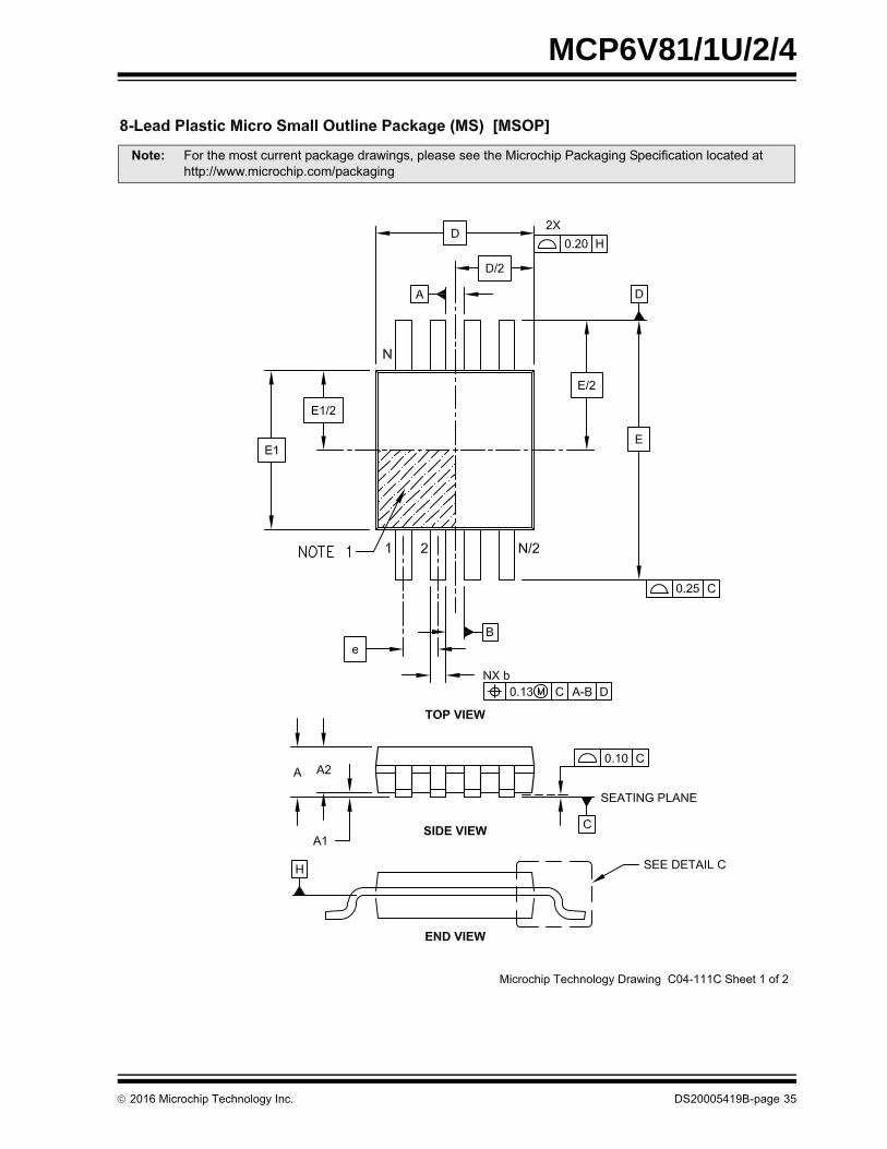
6.0 PACKAGING INFORMATION
6.1 Package Marking Information
5-Lead SC70 (MCP6V81U) Example
5-Lead SOT-23 (MCP6V81, MCP6V81U) Example
Device Code
MCP6V81T-E/OT AABGY
MCP6V81UT-E/OT AABHY
DV56Device Code
MCP6V81UT-E/LTY DVNN
XXXXYWWNNN
AABG5
44256
8-Lead MSOP (MCP6V82) Example
6V82544256
8-Lead TDFN (MCP6V82) Example
ACX54425
Device Code
MCP6V82T-E/MNY ACT
Note: Applies to 8-Lead 2x3 TDFN.
2016 Microchip Technology Inc. DS20005419B-page 29
MCP6V81/1U/2/4
14-Lead TSSOP (MCP6V84) Example
YYWWNNN
XXXXXXXX MCP6V841544
256
Legend: XX...X Customer-specific informationY Year code (last digit of calendar year)YY Year code (last 2 digits of calendar year)WW Week code (week of January 1 is week ‘01’)NNN Alphanumeric traceability code Pb-free JEDEC® designator for Matte Tin (Sn)* This package is Pb-free. The Pb-free JEDEC designator ( )
can be found on the outer packaging for this package.
Note: In the event the full Microchip part number cannot be marked on one line, it willbe carried over to the next line, thus limiting the number of availablecharacters for customer-specific information.
3e3e
DS20005419B-page 30 2016 Microchip Technology Inc.
MCP6V81/1U/2/4
5-Lead Plastic Small Outine Transistor (LTY) [SC70]
Note: For the most current package drawings, please see the Microchip Packaging Specification located at http://www.microchip.com/packaging
2016 Microchip Technology Inc. DS20005419B-page 33
MCP6V81/1U/2/4
Note: For the most current package drawings, please see the Microchip Packaging Specification located at http://www.microchip.com/packaging
DS20005419B-page 34 2016 Microchip Technology Inc.
MCP6V81/1U/2/4
Note: For the most current package drawings, please see the Microchip Packaging Specification located at http://www.microchip.com/packaging
2016 Microchip Technology Inc. DS20005419B-page 35
MCP6V81/1U/2/4
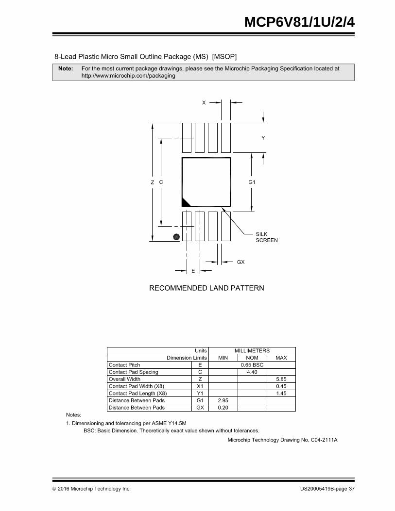
Note: For the most current package drawings, please see the Microchip Packaging Specification located at http://www.microchip.com/packaging
DS20005419B-page 36 2016 Microchip Technology Inc.
MCP6V81/1U/2/4
Note: For the most current package drawings, please see the Microchip Packaging Specification located at http://www.microchip.com/packaging
2016 Microchip Technology Inc. DS20005419B-page 37
MCP6V81/1U/2/4
BA
0.15 C
0.15 C
0.10 C A B0.05 C
(DATUM B)(DATUM A)
CSEATING
PLANE
NOTE 1
1 2
N
2X
TOP VIEW
SIDE VIEW
BOTTOM VIEW
NOTE 1
1 2
N
0.10 C A B
0.10 C A B
0.10 C
0.08 C
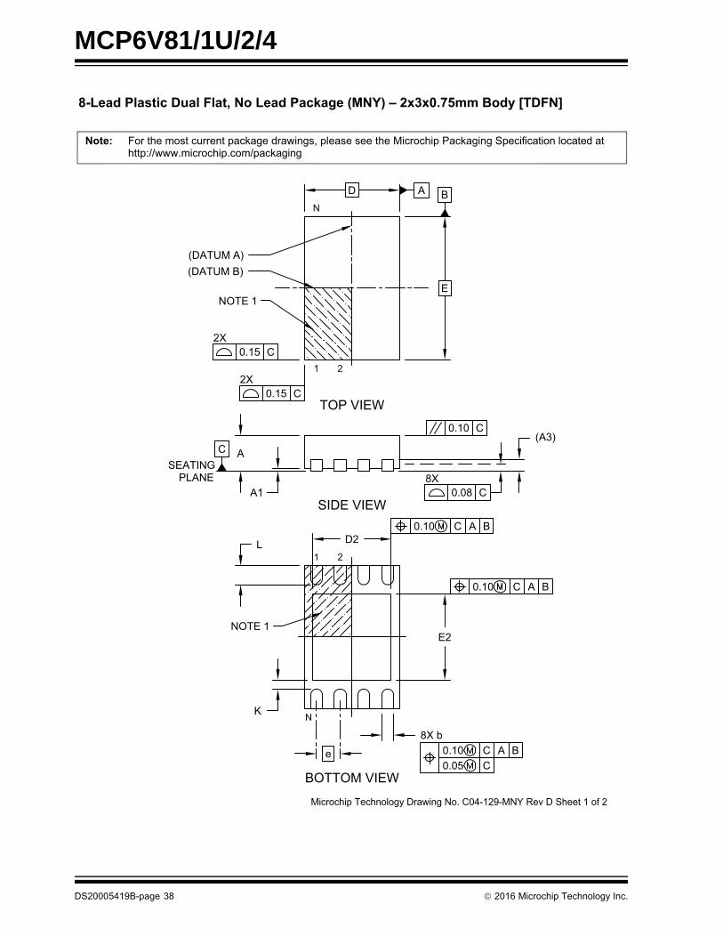
Microchip Technology Drawing No. C04-129-MNY Rev D Sheet of 2
2X
8X
For the most current package drawings, please see the Microchip Packaging Specification located athttp://www.microchip.com/packaging
Note:
8-Lead Plastic Dual Flat, No Lead Package (MNY) – 2x3x0.75mm Body [TDFN]
D
E
D2
E2
A(A3)
A1
e
8X b
L
K
DS20005419B-page 38 2016 Microchip Technology Inc.
MCP6V81/1U/2/4
Microchip Technology Drawing No. C04-129-MNY Rev D Sheet 2 of 2
8-Lead Plastic Dual Flat, No Lead Package (MNY) – 2x3x0.75mm Body [TDFN]
For the most current package drawings, please see the Microchip Packaging Specification located athttp://www.microchip.com/packaging
Note:
NOMMILLIMETERS
0.50 BSC
2.00 BSC3.00 BSC
0.20 REF
1. Pin 1 visual index feature may vary, but must be located within the hatched area.
BSC: Basic Dimension. Theoretically exact value shown without tolerances.REF: Reference Dimension, usually without tolerance, for information purposes only.
Contact-to-Exposed Pad
Contact Thickness
Exposed Pad WidthExposed Pad Length
4. Dimensioning and tolerancing per ASME Y14.5M3. Package is saw singulated2. Package may have one or more exposed tie bars at ends.
Notes:
Contact Width
Overall WidthOverall Length
Contact Length
Standoff
Number of Pins
Overall HeightPitch
K 0.20
Units
NeA
Dimension Limits
DA3A1
b
D2E2
E
L0.20
1.451.60
0.25
0.000.70
MIN
--
0.250.30
--
1.800.300.45
1.65
8
0.750.02 0.05
0.80
MAX
2016 Microchip Technology Inc. DS20005419B-page 39
MCP6V81/1U/2/4
RECOMMENDED LAND PATTERN
Dimension LimitsUnits
Optional Center Pad WidthOptional Center Pad Length
Contact Pitch
Y2X2
1.801.65
MILLIMETERS
0.50 BSCMIN
EMAX
Contact Pad Length (X8)Contact Pad Width (X8)
Y1X1
0.850.25
Microchip Technology Drawing No. C04-129-MNY Rev. A
NOM
8-Lead Plastic Dual Flat, No Lead Package (MNY) – 2x3x0.75mm Body [TDFN]
1 2
8
CContact Pad Spacing 2.90
Thermal Via Diameter VThermal Via Pitch EV
0.301.00
BSC: Basic Dimension. Theoretically exact value shown without tolerances.
Notes:Dimensioning and tolerancing per ASME Y14.5M
For best soldering results, thermal vias, if used, should be filled or tented to avoid solder loss duringreflow process
1.
2.
For the most current package drawings, please see the Microchip Packaging Specification located athttp://www.microchip.com/packaging
Note:
C
E
X1
Y1
Y2
X2
EV
EV
ØV
SILK SCREEN
DS20005419B-page 40 2016 Microchip Technology Inc.
MCP6V81/1U/2/4
Note: For the most current package drawings, please see the Microchip Packaging Specification located at http://www.microchip.com/packaging
2016 Microchip Technology Inc. DS20005419B-page 41
MCP6V81/1U/2/4
Note: For the most current package drawings, please see the Microchip Packaging Specification located at http://www.microchip.com/packaging
DS20005419B-page 42 2016 Microchip Technology Inc.
MCP6V81/1U/2/4
Note: For the most current package drawings, please see the Microchip Packaging Specification located at http://www.microchip.com/packaging
2016 Microchip Technology Inc. DS20005419B-page 43
MCP6V81/1U/2/4
NOTES:
DS20005419B-page 44 2016 Microchip Technology Inc.
2016 Microchip Technology Inc. DS20005419B-page 45
MCP6V81/1U/2/4
APPENDIX A: REVISION HISTORY
Revision B (March 2016)
The following is the list of modifications:
1. Added new devices to the family: MCP6V82 andMCP6V84, and related information throughoutthe document.
2. Added Figure 2-37.
3. Updated Table 3-1 in Section 3.0, PinDescriptions.
4. Added markings and specification drawings forthe new packages in Section 6.0, PackagingInformation.
5. Updated the Product Identification Systemsection with the new packages.
6. Corrected some typographical errors.
Revision A (June 2015)
• Original Release of this Document.
MCP6V81/1U/2/4
DS20005419B-page 46 2016 Microchip Technology Inc.
PRODUCT IDENTIFICATION SYSTEM
To order or obtain information, e.g., on pricing or delivery, refer to the factory or the listed sales office.
Device: MCP6V81T: Single Op Amp (Tape and Reel) (SOT-23 only)
MCP6V81UT: Single Op Amp (Tape and Reel)(SC-70, SOT-23)
MCP6V82: Dual Op Amp (MSOP, 2x3 TDFN)MCP6V82T: Dual Op Amp (Tape and Reel) (MSOP,
2x3 TDFN)MCP6V84: Quad Op Amp (TSSOP)MCP6V84T: Quad Op Amp (Tape and Reel) (TSSOP)
Temperature Range: E = -40°C to +125°C (Extended)
Package: LTY* = Plastic Small Outline Transistor, SC-70, 5-leadOT = Plastic Small Outline Transistor, SOT-23, 5-leadMNY* = Plastic Dual Flat, No-Lead - 2×3×0.75 mm
Body, 8-leadMS = Plastic Micro Small Outline, 8-leadST = Plastic Thin Shrink Small Outline - 4.4 mm
Body, 14-lead
*Y = Nickel palladium gold manufacturing designator. Only available on the SC70 package.
PART NO. –X /XX
PackageTemperatureRange
Device
[X](1)
Tape and Reel
Examples:
a) MCP6V81T-E/OT: Tape and Reel,Extended temperature,5LD SOT-23 package
a) MCP6V81UT-E/LTY: Tape and Reel Extended temperature, 5LD SC70 package
b) MCP6V81UT-E/OT: Tape and Reel,Extended temperature,5LD SOT-23 package
a) MCP6V82-E/MS: Extended temperature, 8LD MSOP package
b) MCP6V82T-E/MS: Tape and Reel, Extended temperature, 8LD MSOP package
c) MCP6V82T-E/MNY: Tape and Reel,Extended temperature,8LD 2x3 TDFN package
a) MCP6V84-E/ST: Extended temperature,14LD TSSOP package
b) MCP6V84T-E/ST: Tape and Reel, Extended temperature, 14LD TSSOP package
Note 1: Tape and Reel identifier only appears in the catalog part number description. This identi-fier is used for ordering purposes and is not printed on the device package. Check with your Microchip Sales Office for package availability with the Tape and Reel option.
Note the following details of the code protection feature on Microchip devices:
• Microchip products meet the specification contained in their particular Microchip Data Sheet.
• Microchip believes that its family of products is one of the most secure families of its kind on the market today, when used in the intended manner and under normal conditions.
• There are dishonest and possibly illegal methods used to breach the code protection feature. All of these methods, to our knowledge, require using the Microchip products in a manner outside the operating specifications contained in Microchip’s Data Sheets. Most likely, the person doing so is engaged in theft of intellectual property.
• Microchip is willing to work with the customer who is concerned about the integrity of their code.
• Neither Microchip nor any other semiconductor manufacturer can guarantee the security of their code. Code protection does not mean that we are guaranteeing the product as “unbreakable.”
Code protection is constantly evolving. We at Microchip are committed to continuously improving the code protection features of ourproducts. Attempts to break Microchip’s code protection feature may be a violation of the Digital Millennium Copyright Act. If such actsallow unauthorized access to your software or other copyrighted work, you may have a right to sue for relief under that Act.
Information contained in this publication regarding deviceapplications and the like is provided only for your convenienceand may be superseded by updates. It is your responsibility toensure that your application meets with your specifications.MICROCHIP MAKES NO REPRESENTATIONS ORWARRANTIES OF ANY KIND WHETHER EXPRESS ORIMPLIED, WRITTEN OR ORAL, STATUTORY OROTHERWISE, RELATED TO THE INFORMATION,INCLUDING BUT NOT LIMITED TO ITS CONDITION,QUALITY, PERFORMANCE, MERCHANTABILITY ORFITNESS FOR PURPOSE. Microchip disclaims all liabilityarising from this information and its use. Use of Microchipdevices in life support and/or safety applications is entirely atthe buyer’s risk, and the buyer agrees to defend, indemnify andhold harmless Microchip from any and all damages, claims,suits, or expenses resulting from such use. No licenses areconveyed, implicitly or otherwise, under any Microchipintellectual property rights unless otherwise stated.
2016 Microchip Technology Inc.
Microchip received ISO/TS-16949:2009 certification for its worldwide headquarters, design and wafer fabrication facilities in Chandler and Tempe, Arizona; Gresham, Oregon and design centers in California and India. The Company’s quality system processes and procedures are for its PIC® MCUs and dsPIC® DSCs, KEELOQ® code hopping devices, Serial EEPROMs, microperipherals, nonvolatile memory and analog products. In addition, Microchip’s quality system for the design and manufacture of development systems is ISO 9001:2000 certified.
QUALITY MANAGEMENT SYSTEM CERTIFIED BY DNV
== ISO/TS 16949 ==
Trademarks
The Microchip name and logo, the Microchip logo, AnyRate, dsPIC, FlashFlex, flexPWR, Heldo, JukeBlox, KeeLoq, KeeLoq logo, Kleer, LANCheck, LINK MD, MediaLB, MOST, MOST logo, MPLAB, OptoLyzer, PIC, PICSTART, PIC32 logo, RightTouch, SpyNIC, SST, SST Logo, SuperFlash and UNI/O are registered trademarks of Microchip Technology Incorporated in the U.S.A. and other countries.
ClockWorks, The Embedded Control Solutions Company, ETHERSYNCH, Hyper Speed Control, HyperLight Load, IntelliMOS, mTouch, Precision Edge, and QUIET-WIRE are registered trademarks of Microchip Technology Incorporated in the U.S.A.
Analog-for-the-Digital Age, Any Capacitor, AnyIn, AnyOut, BodyCom, chipKIT, chipKIT logo, CodeGuard, dsPICDEM, dsPICDEM.net, Dynamic Average Matching, DAM, ECAN, EtherGREEN, In-Circuit Serial Programming, ICSP, Inter-Chip Connectivity, JitterBlocker, KleerNet, KleerNet logo, MiWi, motorBench, MPASM, MPF, MPLAB Certified logo, MPLIB, MPLINK, MultiTRAK, NetDetach, Omniscient Code Generation, PICDEM, PICDEM.net, PICkit, PICtail, PureSilicon, RightTouch logo, REAL ICE, Ripple Blocker, Serial Quad I/O, SQI, SuperSwitcher, SuperSwitcher II, Total Endurance, TSHARC, USBCheck, VariSense, ViewSpan, WiperLock, Wireless DNA, and ZENA are trademarks of Microchip Technology Incorporated in the U.S.A. and other countries.
SQTP is a service mark of Microchip Technology Incorporated in the U.S.A.
Silicon Storage Technology is a registered trademark of Microchip Technology Inc. in other countries.
GestIC is a registered trademarks of Microchip Technology Germany II GmbH & Co. KG, a subsidiary of Microchip Technology Inc., in other countries.
All other trademarks mentioned herein are property of their respective companies.