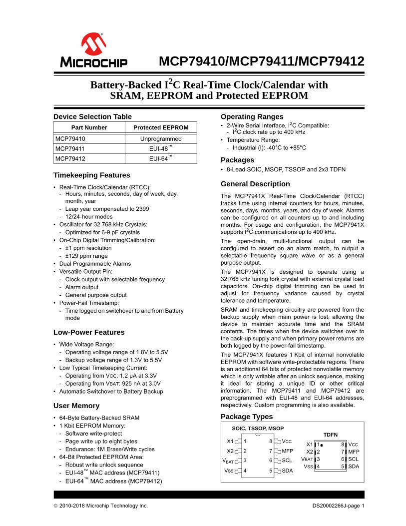
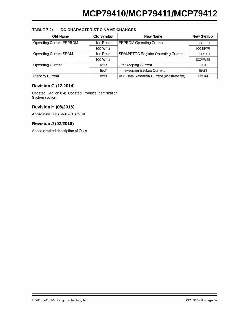
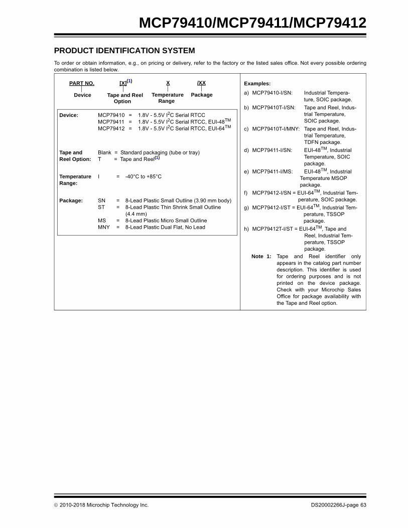
2010-2018 Microchip Technology Inc. DS20002266J-page 1 MCP79410/MCP79411/MCP79412 Device Selection Table Timekeeping Features • Real-Time Clock/Calendar (RTCC): - Hours, minutes, seconds, day of week, day, month, year - Leap year compensated to 2399 - 12/24-hour modes • Oscillator for 32.768 kHz Crystals: - Optimized for 6-9 pF crystals • On-Chip Digital Trimming/Calibration: - ±1 ppm resolution - ±129 ppm range • Dual Programmable Alarms • Versatile Output Pin: - Clock output with selectable frequency - Alarm output - General purpose output • Power-Fail Timestamp: - Time logged on switchover to and from Battery mode Low-Power Features • Wide Voltage Range: - Operating voltage range of 1.8V to 5.5V - Backup voltage range of 1.3V to 5.5V • Low Typical Timekeeping Current: - Operating from VCC: 1.2 μA at 3.3V - Operating from VBAT: 925 nA at 3.0V • Automatic Switchover to Battery Backup User Memory • 64-Byte Battery-Backed SRAM • 1 Kbit EEPROM Memory: - Software write-protect - Page write up to eight bytes - Endurance: 1M Erase/Write cycles • 64-Bit Protected EEPROM Area: - Robust write unlock sequence - EUI-48 ™ MAC address (MCP79411) - EUI-64 ™ MAC address (MCP79412) Operating Ranges • 2-Wire Serial Interface, I 2 C Compatible: -I 2 C clock rate up to 400 kHz • Temperature Range: - Industrial (I): -40°C to +85°C Packages • 8-Lead SOIC, MSOP, TSSOP and 2x3 TDFN General Description The MCP7941X Real-Time Clock/Calendar (RTCC) tracks time using internal counters for hours, minutes, seconds, days, months, years, and day of week. Alarms can be configured on all counters up to and including months. For usage and configuration, the MCP7941X supports I 2 C communications up to 400 kHz. The open-drain, multi-functional output can be configured to assert on an alarm match, to output a selectable frequency square wave or as a general purpose output. The MCP7941X is designed to operate using a 32.768 kHz tuning fork crystal with external crystal load capacitors. On-chip digital trimming can be used to adjust for frequency variance caused by crystal tolerance and temperature. SRAM and timekeeping circuitry are powered from the backup supply when main power is lost, allowing the device to maintain accurate time and the SRAM contents. The times when the device switches over to the back-up supply and when primary power returns are both logged by the power-fail timestamp. The MCP7941X features 1 Kbit of internal nonvolatile EEPROM with software write-protectable regions. There is an additional 64 bits of protected nonvolatile memory which is only writable after an unlock sequence, making it ideal for storing a unique ID or other critical information. The MCP79411 and MCP79412 are preprogrammed with EUI-48 and EUI-64 addresses, respectively. Custom programming is also available. Package Types Part Number Protected EEPROM MCP79410 Unprogrammed MCP79411 EUI-48 ™ MCP79412 EUI-64 ™ SOIC, TSSOP, MSOP X1 X2 V BAT VSS 1 2 3 4 8 7 6 5 VCC MFP SCL SDA TDFN X1 X2 VSS MFP SDA VCC 8 7 5 1 2 4 VBAT 3 SCL 6 Battery-Backed I 2 C Real-Time Clock/Calendar with SRAM, EEPROM and Protected EEPROM
Transcript
MCP79410/MCP79411/MCP79412
Battery-Backed I2C Real-Time Clock/Calendar withSRAM, EEPROM and Protected EEPROM
Device Selection Table
Timekeeping Features
• Real-Time Clock/Calendar (RTCC):- Hours, minutes, seconds, day of week, day,
month, year- Leap year compensated to 2399- 12/24-hour modes
• Oscillator for 32.768 kHz Crystals:- Optimized for 6-9 pF crystals
• On-Chip Digital Trimming/Calibration:- ±1 ppm resolution- ±129 ppm range
• Dual Programmable Alarms• Versatile Output Pin:
- Clock output with selectable frequency- Alarm output- General purpose output
• Power-Fail Timestamp:- Time logged on switchover to and from Battery
mode
Low-Power Features
• Wide Voltage Range:- Operating voltage range of 1.8V to 5.5V- Backup voltage range of 1.3V to 5.5V
• Low Typical Timekeeping Current:- Operating from VCC: 1.2 µA at 3.3V- Operating from VBAT: 925 nA at 3.0V
Operating Ranges• 2-Wire Serial Interface, I2C Compatible:
- I2C clock rate up to 400 kHz• Temperature Range:
- Industrial (I): -40°C to +85°C
Packages• 8-Lead SOIC, MSOP, TSSOP and 2x3 TDFN
General Description
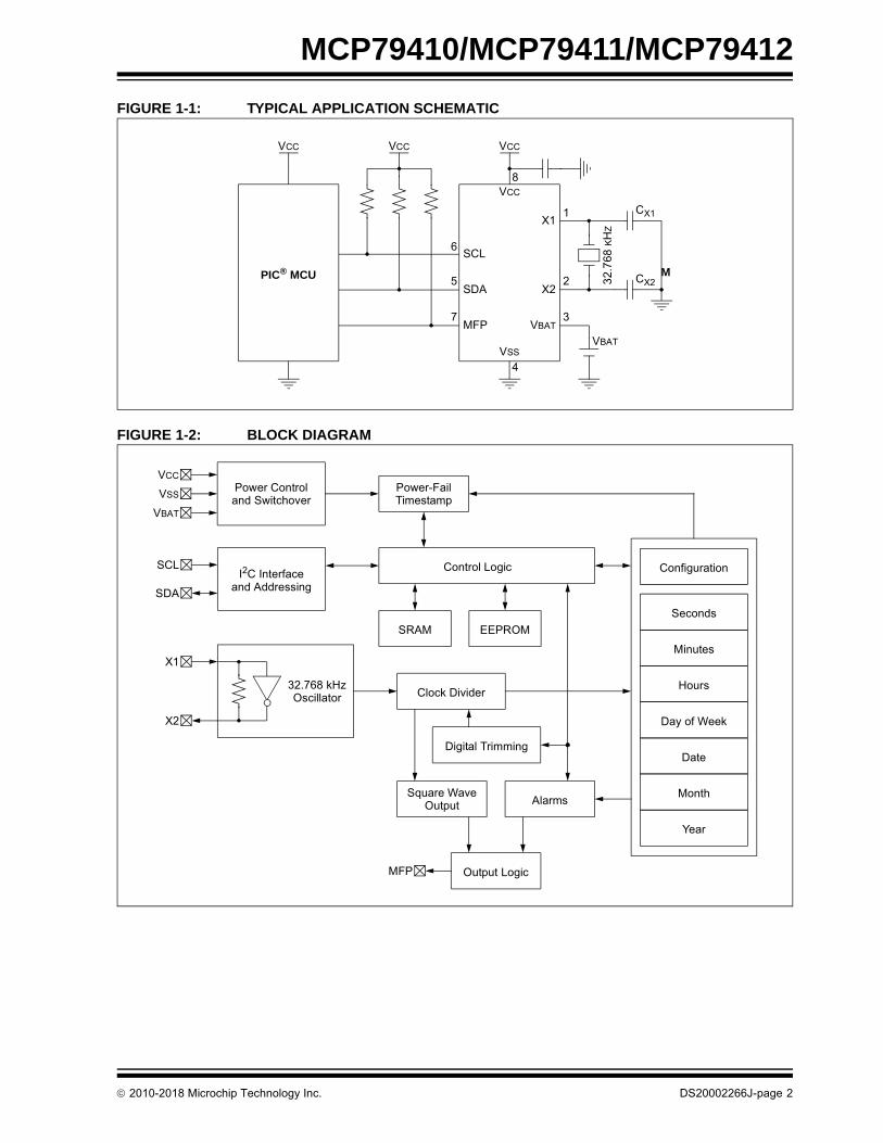
The MCP7941X Real-Time Clock/Calendar (RTCC)tracks time using internal counters for hours, minutes,seconds, days, months, years, and day of week. Alarmscan be configured on all counters up to and includingmonths. For usage and configuration, the MCP7941Xsupports I2C communications up to 400 kHz.
The open-drain, multi-functional output can beconfigured to assert on an alarm match, to output aselectable frequency square wave or as a generalpurpose output.
The MCP7941X is designed to operate using a32.768 kHz tuning fork crystal with external crystal loadcapacitors. On-chip digital trimming can be used toadjust for frequency variance caused by crystaltolerance and temperature.
SRAM and timekeeping circuitry are powered from thebackup supply when main power is lost, allowing thedevice to maintain accurate time and the SRAMcontents. The times when the device switches over tothe back-up supply and when primary power returns areboth logged by the power-fail timestamp.
The MCP7941X features 1 Kbit of internal nonvolatileEEPROM with software write-protectable regions. Thereis an additional 64 bits of protected nonvolatile memorywhich is only writable after an unlock sequence, makingit ideal for storing a unique ID or other criticalinformation. The MCP79411 and MCP79412 arepreprogrammed with EUI-48 and EUI-64 addresses,respectively. Custom programming is also available.
Package Types
Part Number Protected EEPROM
MCP79410 Unprogrammed
MCP79411 EUI-48™
MCP79412 EUI-64™
SOIC, TSSOP, MSOP
X1
X2
VBAT
VSS
1
2
3
4
8
7
6
5
VCC
MFP
SCL
SDA
TDFN
X1X2
VSS
MFP
SDA
VCC87
5
12
4VBAT 3 SCL6
2010-2018 Microchip Technology Inc. DS20002266J-page 1
MCP79410/MCP79411/MCP79412
FIGURE 1-1: TYPICAL APPLICATION SCHEMATIC
FIGURE 1-2: BLOCK DIAGRAM
VCC VCCVCC
VBAT
CX1
32
.76
8 K
HZ
CX2
VBAT
X2
X1
SCL
SDA
MFP
VSS
VCC
1
2
3
4
5
7
6
8
PIC® MCU M
32.768 kHz
I2C Interfaceand Addressing
Control Logic
SRAM EEPROM
Clock Divider
Digital Trimming
Square WaveOutput Alarms
Output Logic
Seconds
Minutes
Hours
Day of Week
Date
Month
Year
Configuration
Oscillator
X1
X2
SCL
SDA
MFP
Power Controland Switchover
VCC
VBAT
Power-FailTimestamp
VSS
2010-2018 Microchip Technology Inc. DS20002266J-page 2
All inputs and outputs (except SDA and SCL) w.r.t. VSS.....................................................................-0.6V to VCC +1.0V
SDA and SCL w.r.t. VSS ............................................................................................................................... -0.6V to 6.5V
Storage temperature ............................................................................................................................... -65°C to +150°C
Ambient temperature with power applied................................................................................................-40°C to +125°C
ESD protection on all pins........................................................................................................................................≥4 kV
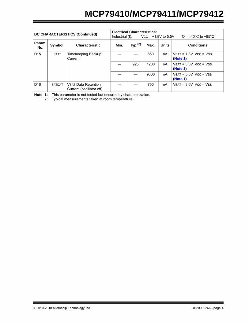
TABLE 1-1: DC CHARACTERISTICS
† NOTICE: Stresses above those listed under “Absolute Maximum Ratings” may cause permanent damage to thedevice. This is a stress rating only and functional operation of the device at those or any other conditions above thoseindicated in the operational listings of this specification is not implied. Exposure to maximum rating conditions forextended periods may affect device reliability.
DC CHARACTERISTICSElectrical Characteristics:Industrial (I): VCC = +1.8V to 5.5V TA = -40°C to +85°C
Param.No.
Symbol Characteristic Min. Typ.(2) Max. Units Conditions
D1 VIH High-Level Input Voltage 0.7 VCC — — V
D2 VIL Low-Level Input Voltage — — 0.3 VCC V VCC ≥ 2.5V
— — 0.2 VCC V VCC < 2.5V
D3 VHYS Hysteresis of Schmitt Trigger Inputs(SDA, SCL pins)
0.05 VCC — — V Note 1
D4 VOL Low-Level Output Voltage(MFP, SDA pins)
— — 0.40 V IOL = 3.0 mA; VCC = 4.5V
— — 0.40 V IOL = 2.1 mA; VCC = 2.5V
D5 ILI Input Leakage Current — — ±1 µA VIN = VSS or VCC
D6 ILO Output Leakage Current — — ±1 µA VOUT = VSS or VCC
D7 CIN, COUT
Pin Capacitance (SDA, SCL, MFP pins)
— — 10 pF VCC = 5.0V (Note 1)
— — 10 pF TA = 25°C, f = 1 MHz
D8 COSC Oscillator Pin Capacitance (X1, X2 pins)
— 3 — pF Note 1
D9 ICCEERD EEPROM OperatingCurrent
— — 400 µA VCC = 5.5V, SCL = 400 kHz
ICCEEWR — — 3 mA VCC = 5.5V
D10 ICCREAD, ICCWRITE
SRAM/RTCC Register Operating Current
— — 300 µA VCC = 5.5V, SCL = 400 kHz
— — 400 µA VCC = 5.5V, SCL = 400 kHz
D11 ICCDAT VCC Data-Retention Current (oscillator off)
2: This parameter is not tested but ensured by characterization.
3: As a transmitter, the device must provide an internal minimum delay time to bridge the undefined region (minimum 300 ns) of the falling edge of SCL to avoid unintended generation of Start or Stop conditions.
2010-2018 Microchip Technology Inc. DS20002266J-page 5
MCP79410/MCP79411/MCP79412
FIGURE 1-3: I2C BUS TIMING DATA
FIGURE 1-4: POWER SUPPLY TRANSITION TIMING
SCL
SDAIn
SDAOut
5
7
6
13
3
2
8 9
11
D3 4
10
12
VCC
VTRIP(MAX)
VTRIP(MIN)
15 16
2010-2018 Microchip Technology Inc. DS20002266J-page 6
MCP79410/MCP79411/MCP79412
2.0 TYPICAL PERFORMANCE CURVE
FIGURE 2-1: TIMEKEEPING BACKUP CURRENT VS. BACKUP SUPPLY VOLTAGE
Note: The graphs and tables provided following this note are a statistical summary based on a limited number ofsamples and are provided for informational purposes only. The performance characteristics listed hereinare not tested or guaranteed. In some graphs or tables, the data represented may be outside the specifiedoperating range (e.g., outside specified power supply range) and therefore, outside the warranted range.
0.0
0.5
1.0
1.5
2.0
2.5
3.0
3.5
4.0
4.5
5.0
5.5
1.30 1.90 2.50 3.10 3.70 4.30 4.90 5.50
IBA
TT C
urr
en
t (µ
A)
VBAT Voltage (V)
-40
25
85
TA = -40°C TA = 25°C TA = 85°C
2010-2018 Microchip Technology Inc. DS20002266J-page 7
MCP79410/MCP79411/MCP79412
3.0 PIN DESCRIPTIONS
The descriptions of the pins are listed in Table 3-1.
TABLE 3-1: PIN FUNCTION TABLE
3.1 Oscillator Input/Output (X1, X2)
These pins are used as the connections for an external32.768 kHz quartz crystal and load capacitors. X1 isthe crystal oscillator input and X2 is the output. TheMCP7941X is designed to allow for the use of externalload capacitors in order to provide additional flexibilitywhen choosing external crystals. The MCP7941X isoptimized for crystals with a specified load capacitanceof 6-9 pF.
X1 also serves as the external clock input when theMCP7941X is configured to use an external oscillator.
3.2 Backup Supply (VBAT)
This is the input for a backup supply to maintain theRTCC and SRAM registers during the time when VCC
is unavailable.
If the battery backup feature is not being used, theVBAT pin should be connected to VSS.
3.3 Serial Data (SDA)
This is a bidirectional pin used to transfer addressesand data into and out of the device. It is an open-drainterminal. Therefore, the SDA bus requires a pull-upresistor to VCC (typically 10 kΩ for 100 kHz, 2 kΩ for400 kHz). For normal data transfer, SDA is allowed tochange only during SCL low. Changes during SCL highare reserved for indicating the Start and Stopconditions.
3.4 Serial Clock (SCL)
This input is used to synchronize the data transfer toand from the device.
3.5 Multifunction Pin (MFP)
This is an output pin used for the alarm and squarewave output functions. It can also serve as a generalpurpose output pin by controlling the OUT bit in theCONTROL register.
The MFP is an open-drain output and requires a pull-upresistor to VCC (typically 10 kΩ). This pin may be leftfloating if not used.
Note: Exposed pad on TDFN can be connected to VSS or left floating.
2010-2018 Microchip Technology Inc. DS20002266J-page 8
MCP79410/MCP79411/MCP79412
4.0 I2C BUS CHARACTERISTICS
4.1 I2C Interface
The MCP7941X supports a bidirectional 2-wire bus anddata transmission protocol. A device that sends dataonto the bus is defined as transmitter, and a devicereceiving data is defined as receiver. The bus has to becontrolled by a master device which generates the Startand Stop conditions, while the MCP7941X works asslave. Both master and slave can operate astransmitter or receiver, but the master devicedetermines which mode is activated.
4.1.1 BUS CHARACTERISTICS
The following bus protocol has been defined:
• Data transfer may be initiated only when the bus is not busy.
• During data transfer, the data line must remain stable whenever the clock line is high. Changes in the data line while the clock line is high will be interpreted as a Start or Stop condition.
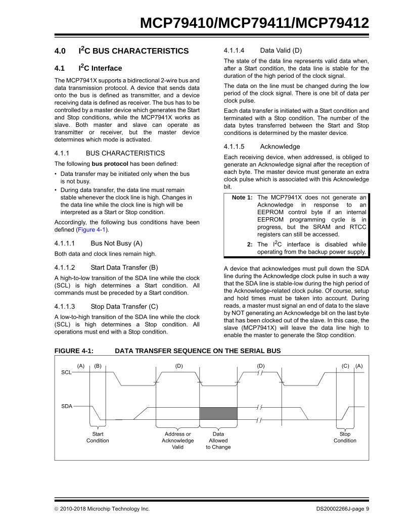
Accordingly, the following bus conditions have beendefined (Figure 4-1).
4.1.1.1 Bus Not Busy (A)
Both data and clock lines remain high.
4.1.1.2 Start Data Transfer (B)
A high-to-low transition of the SDA line while the clock(SCL) is high determines a Start condition. Allcommands must be preceded by a Start condition.
4.1.1.3 Stop Data Transfer (C)
A low-to-high transition of the SDA line while the clock(SCL) is high determines a Stop condition. Alloperations must end with a Stop condition.
4.1.1.4 Data Valid (D)
The state of the data line represents valid data when,after a Start condition, the data line is stable for theduration of the high period of the clock signal.
The data on the line must be changed during the lowperiod of the clock signal. There is one bit of data perclock pulse.
Each data transfer is initiated with a Start condition andterminated with a Stop condition. The number of thedata bytes transferred between the Start and Stopconditions is determined by the master device.
4.1.1.5 Acknowledge
Each receiving device, when addressed, is obliged togenerate an Acknowledge signal after the reception ofeach byte. The master device must generate an extraclock pulse which is associated with this Acknowledgebit.
A device that acknowledges must pull down the SDAline during the Acknowledge clock pulse in such a waythat the SDA line is stable-low during the high period ofthe Acknowledge-related clock pulse. Of course, setupand hold times must be taken into account. Duringreads, a master must signal an end of data to the slaveby NOT generating an Acknowledge bit on the last bytethat has been clocked out of the slave. In this case, theslave (MCP7941X) will leave the data line high toenable the master to generate the Stop condition.
FIGURE 4-1: DATA TRANSFER SEQUENCE ON THE SERIAL BUS
Note 1: The MCP7941X does not generate anAcknowledge in response to anEEPROM control byte if an internalEEPROM programming cycle is inprogress, but the SRAM and RTCCregisters can still be accessed.
2: The I2C interface is disabled whileoperating from the backup power supply.
Address orAcknowledge
Valid
DataAllowed
to Change
StopCondition
StartCondition
SCL
SDA
(A) (B) (D) (D) (C) (A)
2010-2018 Microchip Technology Inc. DS20002266J-page 9
MCP79410/MCP79411/MCP79412
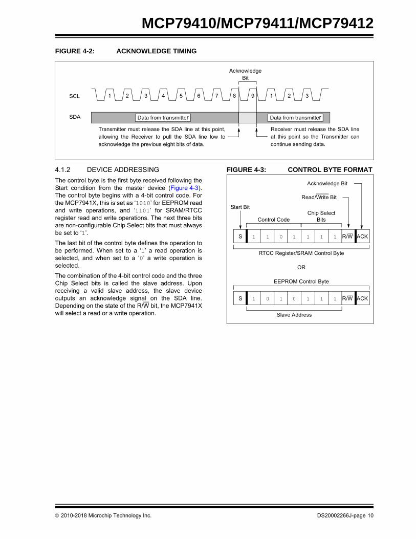
FIGURE 4-2: ACKNOWLEDGE TIMING
4.1.2 DEVICE ADDRESSING
The control byte is the first byte received following theStart condition from the master device (Figure 4-3).The control byte begins with a 4-bit control code. Forthe MCP7941X, this is set as ‘1010’ for EEPROM readand write operations, and ‘1101’ for SRAM/RTCCregister read and write operations. The next three bitsare non-configurable Chip Select bits that must alwaysbe set to ‘1’.
The last bit of the control byte defines the operation tobe performed. When set to a ‘1’ a read operation isselected, and when set to a ‘0’ a write operation isselected.
The combination of the 4-bit control code and the threeChip Select bits is called the slave address. Uponreceiving a valid slave address, the slave deviceoutputs an acknowledge signal on the SDA line.Depending on the state of the R/W bit, the MCP7941Xwill select a read or a write operation.
FIGURE 4-3: CONTROL BYTE FORMAT
SCL 987654321 1 2 3
Transmitter must release the SDA line at this point,allowing the Receiver to pull the SDA line low toacknowledge the previous eight bits of data.
Receiver must release the SDA lineat this point so the Transmitter cancontinue sending data.
Data from transmitterSDA
AcknowledgeBit
Data from transmitter
1 1 0 1 1 1 1S ACKR/W
Control CodeChip Select
Bits
Slave Address
Acknowledge Bit
Start Bit
Read/Write Bit
1 0 1 0 1 1 1S ACKR/W
OR
EEPROM Control Byte
RTCC Register/SRAM Control Byte
2010-2018 Microchip Technology Inc. DS20002266J-page 10
MCP79410/MCP79411/MCP79412
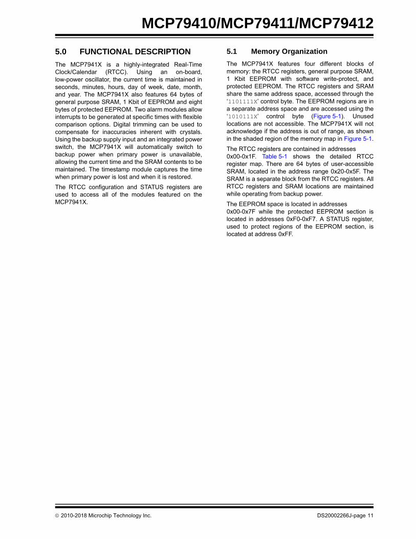
5.0 FUNCTIONAL DESCRIPTION
The MCP7941X is a highly-integrated Real-TimeClock/Calendar (RTCC). Using an on-board,low-power oscillator, the current time is maintained inseconds, minutes, hours, day of week, date, month,and year. The MCP7941X also features 64 bytes ofgeneral purpose SRAM, 1 Kbit of EEPROM and eightbytes of protected EEPROM. Two alarm modules allowinterrupts to be generated at specific times with flexiblecomparison options. Digital trimming can be used tocompensate for inaccuracies inherent with crystals.Using the backup supply input and an integrated powerswitch, the MCP7941X will automatically switch tobackup power when primary power is unavailable,allowing the current time and the SRAM contents to bemaintained. The timestamp module captures the timewhen primary power is lost and when it is restored.
The RTCC configuration and STATUS registers areused to access all of the modules featured on theMCP7941X.
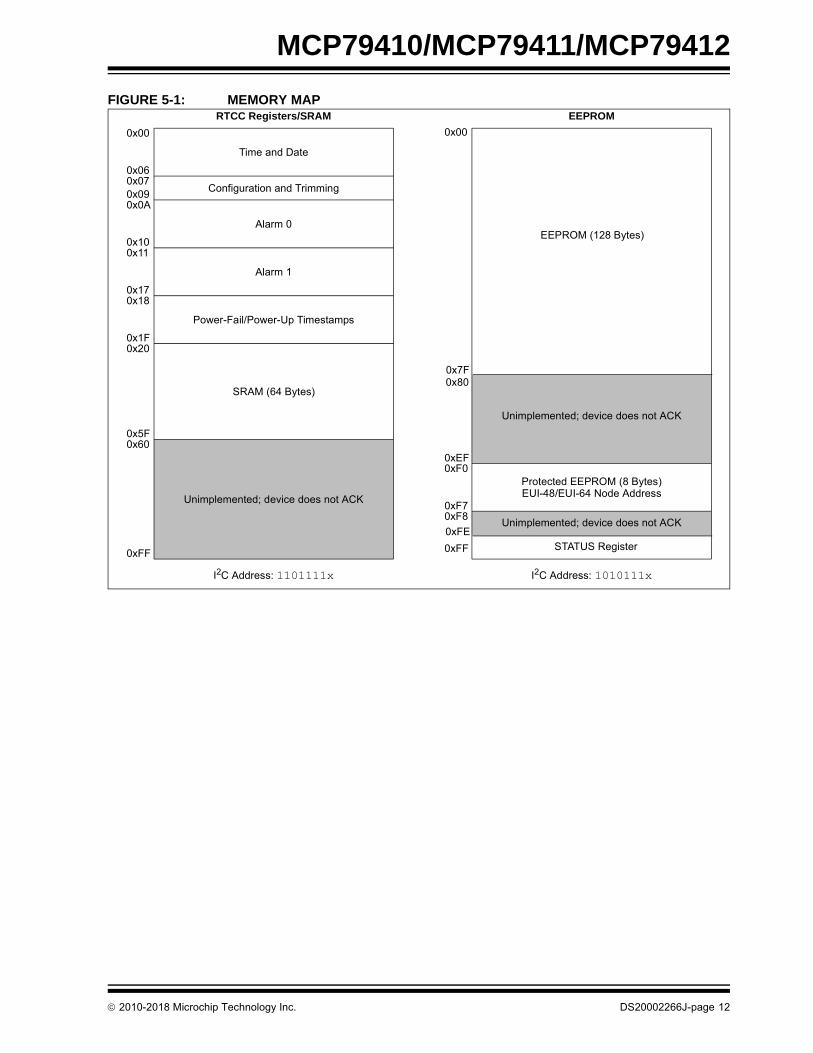
5.1 Memory Organization
The MCP7941X features four different blocks ofmemory: the RTCC registers, general purpose SRAM,1 Kbit EEPROM with software write-protect, andprotected EEPROM. The RTCC registers and SRAMshare the same address space, accessed through the‘1101111X’ control byte. The EEPROM regions are ina separate address space and are accessed using the‘1010111X’ control byte (Figure 5-1). Unusedlocations are not accessible. The MCP7941X will notacknowledge if the address is out of range, as shownin the shaded region of the memory map in Figure 5-1.
The RTCC registers are contained in addresses 0x00-0x1F. Table 5-1 shows the detailed RTCCregister map. There are 64 bytes of user-accessibleSRAM, located in the address range 0x20-0x5F. TheSRAM is a separate block from the RTCC registers. AllRTCC registers and SRAM locations are maintainedwhile operating from backup power.
The EEPROM space is located in addresses 0x00-0x7F while the protected EEPROM section islocated in addresses 0xF0-0xF7. A STATUS register,used to protect regions of the EEPROM section, islocated at address 0xFF.
2010-2018 Microchip Technology Inc. DS20002266J-page 11
MCP79410/MCP79411/MCP79412
FIGURE 5-1: MEMORY MAP
Time and Date
SRAM (64 Bytes)
Power-Fail/Power-Up Timestamps
Alarm 1
Alarm 0
Configuration and Trimming
0x00
0x060x070x090x0A
0x100x11
0x170x18
0x1F0x20
0x5F0x60
0xFF
Unimplemented; device does not ACK
I2C Address: 1101111x
RTCC Registers/SRAM
Protected EEPROM (8 Bytes)
0x00
0xEF0xF0
0xF70xF8
0xFF
Unimplemented; device does not ACK
I2C Address: 1010111x
EEPROM
EUI-48/EUI-64 Node Address
Unimplemented; device does not ACK
0x7F0x80
EEPROM (128 Bytes)
0xFE
STATUS Register
2010-2018 Microchip Technology Inc. DS20002266J-page 12
MCP79410/MCP79411/MCP79412
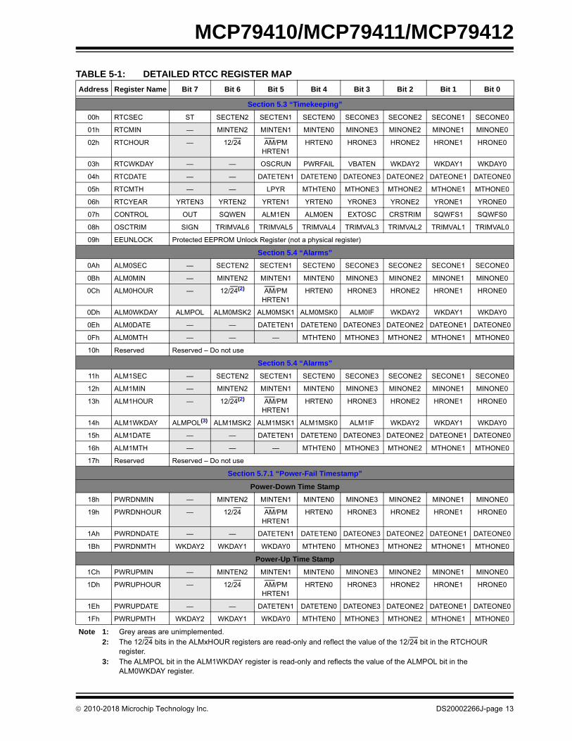
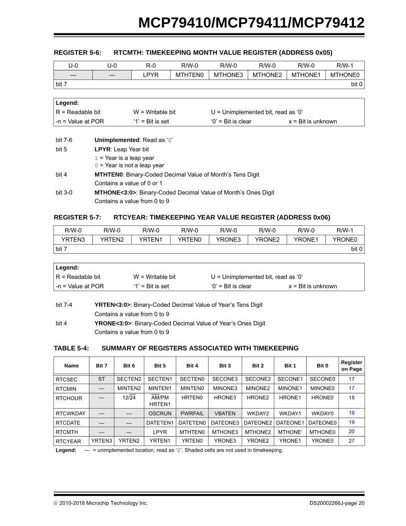
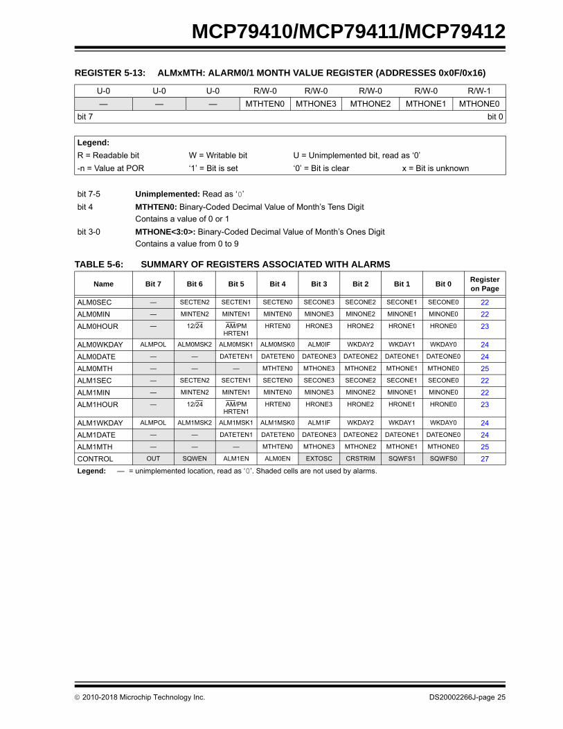
TABLE 5-1: DETAILED RTCC REGISTER MAP
Address Register Name Bit 7 Bit 6 Bit 5 Bit 4 Bit 3 Bit 2 Bit 1 Bit 0
Section 5.3 “Timekeeping”
00h RTCSEC ST SECTEN2 SECTEN1 SECTEN0 SECONE3 SECONE2 SECONE1 SECONE0
Note 1: Grey areas are unimplemented.2: The 12/24 bits in the ALMxHOUR registers are read-only and reflect the value of the 12/24 bit in the RTCHOUR
register.3: The ALMPOL bit in the ALM1WKDAY register is read-only and reflects the value of the ALMPOL bit in the
ALM0WKDAY register.
2010-2018 Microchip Technology Inc. DS20002266J-page 13
MCP79410/MCP79411/MCP79412
5.2 Oscillator Configuration
The MCP7941X can be operated in two differentoscillator configurations: using an external crystal orusing an external clock input.
5.2.1 EXTERNAL CRYSTAL
The crystal oscillator circuit on the MCP7941X isdesigned to operate with a standard 32.768 kHz tuningfork crystal and matching external load capacitors. Byusing external load capacitors, the MCP7941X allowsfor a wide selection of crystals. Suitable crystals have aload capacitance (CL) of 6-9 pF. Crystals with a loadcapacitance of 12.5 pF are not recommended.
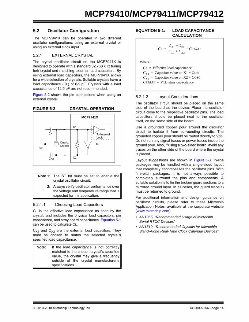
Figure 5-2 shows the pin connections when using anexternal crystal.
FIGURE 5-2: CRYSTAL OPERATION
5.2.1.1 Choosing Load Capacitors
CL is the effective load capacitance as seen by thecrystal, and includes the physical load capacitors, pincapacitance, and stray board capacitance. Equation 5-1can be used to calculate CL.
CX1 and CX2 are the external load capacitors. Theymust be chosen to match the selected crystal’sspecified load capacitance.
EQUATION 5-1: LOAD CAPACITANCE CALCULATION
5.2.1.2 Layout Considerations
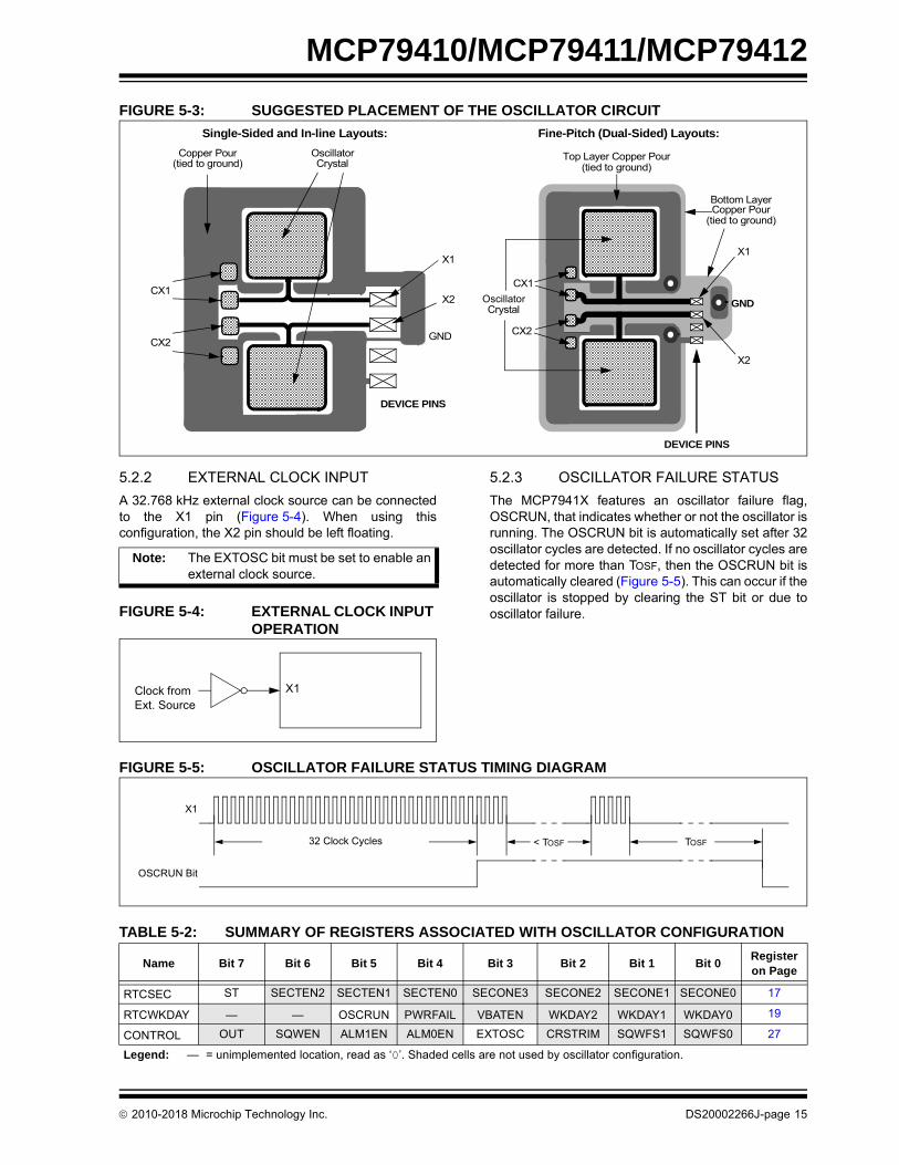
The oscillator circuit should be placed on the sameside of the board as the device. Place the oscillatorcircuit close to the respective oscillator pins. The loadcapacitors should be placed next to the oscillatoritself, on the same side of the board.
Use a grounded copper pour around the oscillatorcircuit to isolate it from surrounding circuits. Thegrounded copper pour should be routed directly to VSS.Do not run any signal traces or power traces inside theground pour. Also, if using a two-sided board, avoid anytraces on the other side of the board where the crystalis placed.
Layout suggestions are shown in Figure 5-3. In-linepackages may be handled with a single-sided layoutthat completely encompasses the oscillator pins. Withfine-pitch packages, it is not always possible tocompletely surround the pins and components. Asuitable solution is to tie the broken guard sections to amirrored ground layer. In all cases, the guard trace(s)must be returned to ground.
For additional information and design guidance onoscillator circuits, please refer to these MicrochipApplication Notes, available at the corporate website(www.microchip.com):
• AN1365, “Recommended Usage of Microchip Serial RTCC Devices”
Note 1: The ST bit must be set to enable thecrystal oscillator circuit.
2: Always verify oscillator performance overthe voltage and temperature range that isexpected for the application.
Note: If the load capacitance is not correctlymatched to the chosen crystal’s specifiedvalue, the crystal may give a frequencyoutside of the crystal manufacturer’sspecifications.
CL Effective load capacitance=CX1 Capacitor value on X1 COSC+=CX2 Capacitor value on X2 COSC+=CSTRAY PCB stray capacitance=
2010-2018 Microchip Technology Inc. DS20002266J-page 14
MCP79410/MCP79411/MCP79412
FIGURE 5-3: SUGGESTED PLACEMENT OF THE OSCILLATOR CIRCUIT
5.2.2 EXTERNAL CLOCK INPUT
A 32.768 kHz external clock source can be connectedto the X1 pin (Figure 5-4). When using thisconfiguration, the X2 pin should be left floating.
FIGURE 5-4: EXTERNAL CLOCK INPUT OPERATION
5.2.3 OSCILLATOR FAILURE STATUS
The MCP7941X features an oscillator failure flag,OSCRUN, that indicates whether or not the oscillator isrunning. The OSCRUN bit is automatically set after 32oscillator cycles are detected. If no oscillator cycles aredetected for more than TOSF, then the OSCRUN bit isautomatically cleared (Figure 5-5). This can occur if theoscillator is stopped by clearing the ST bit or due tooscillator failure.
FIGURE 5-5: OSCILLATOR FAILURE STATUS TIMING DIAGRAM
TABLE 5-2: SUMMARY OF REGISTERS ASSOCIATED WITH OSCILLATOR CONFIGURATION
GND
`
X1
X2
DEVICE PINS
CX1
CX2
GND
X1
X2
Bottom LayerCopper Pour
OscillatorCrystal
Top Layer Copper Pour
CX1
CX2
DEVICE PINS
(tied to ground)
(tied to ground)
Single-Sided and In-line Layouts: Fine-Pitch (Dual-Sided) Layouts:
OscillatorCrystal
Copper Pour(tied to ground)
Note: The EXTOSC bit must be set to enable anexternal clock source.
X1Clock fromExt. Source
Name Bit 7 Bit 6 Bit 5 Bit 4 Bit 3 Bit 2 Bit 1 Bit 0Register on Page
RTCSEC ST SECTEN2 SECTEN1 SECTEN0 SECONE3 SECONE2 SECONE1 SECONE0 17
CONTROL OUT SQWEN ALM1EN ALM0EN EXTOSC CRSTRIM SQWFS1 SQWFS0 27
Legend: — = unimplemented location, read as ‘0’. Shaded cells are not used by oscillator configuration.
X1
OSCRUN Bit
< TOSF TOSF32 Clock Cycles
2010-2018 Microchip Technology Inc. DS20002266J-page 15
MCP79410/MCP79411/MCP79412
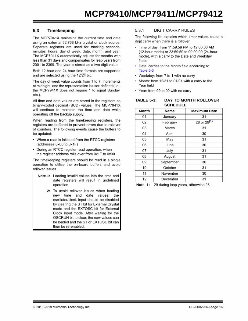
5.3 Timekeeping
The MCP7941X maintains the current time and dateusing an external 32.768 kHz crystal or clock source.Separate registers are used for tracking seconds,minutes, hours, day of week, date, month, and year.The MCP7941X automatically adjusts for months withless than 31 days and compensates for leap years from2001 to 2399. The year is stored as a two-digit value.
Both 12-hour and 24-hour time formats are supportedand are selected using the 12/24 bit.
The day of week value counts from 1 to 7, incrementsat midnight, and the representation is user-defined (i.e.,the MCP7941X does not require 1 to equal Sunday,etc.).
All time and date values are stored in the registers asbinary-coded decimal (BCD) values. The MCP7941Xwill continue to maintain the time and date whileoperating off the backup supply.
When reading from the timekeeping registers, theregisters are buffered to prevent errors due to rolloverof counters. The following events cause the buffers tobe updated:
• When a read is initiated from the RTCC registers (addresses 0x00 to 0x1F)
• During an RTCC register read operation, when the register address rolls over from 0x1F to 0x00
The timekeeping registers should be read in a singleoperation to utilize the on-board buffers and avoidrollover issues.
5.3.1 DIGIT CARRY RULES
The following list explains which timer values cause adigit carry when there is a rollover:
• Time of day: from 11:59:59 PM to 12:00:00 AM (12-hour mode) or 23:59:59 to 00:00:00 (24-hour mode), with a carry to the Date and Weekday fields
• Date: carries to the Month field according to Table 5-3
• Weekday: from 7 to 1 with no carry
• Month: from 12/31 to 01/01 with a carry to the Year field
• Year: from 99 to 00 with no carry
TABLE 5-3: DAY TO MONTH ROLLOVER SCHEDULE
Note 1: Loading invalid values into the time anddate registers will result in undefinedoperation.
2: To avoid rollover issues when loadingnew time and date values, theoscillator/clock input should be disabledby clearing the ST bit for External Crystalmode and the EXTOSC bit for ExternalClock Input mode. After waiting for theOSCRUN bit to clear, the new values canbe loaded and the ST or EXTOSC bit canthen be re-enabled.
Month Name Maximum Date
01 January 31
02 February 28 or 29(1)
03 March 31
04 April 30
05 May 31
06 June 30
07 July 31
08 August 31
09 September 30
10 October 31
11 November 30
12 December 31
Note 1: 29 during leap years, otherwise 28.
2010-2018 Microchip Technology Inc. DS20002266J-page 16
MCP79410/MCP79411/MCP79412
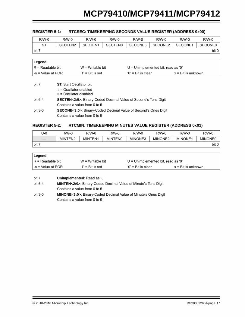
REGISTER 5-1: RTCSEC: TIMEKEEPING SECONDS VALUE REGISTER (ADDRESS 0x00)
R/W-0 R/W-0 R/W-0 R/W-0 R/W-0 R/W-0 R/W-0 R/W-0
ST SECTEN2 SECTEN1 SECTEN0 SECONE3 SECONE2 SECONE1 SECONE0
bit 7 bit 0
Legend:
R = Readable bit W = Writable bit U = Unimplemented bit, read as ‘0’
-n = Value at POR ‘1’ = Bit is set ‘0’ = Bit is clear x = Bit is unknown
bit 7 ST: Start Oscillator bit
1 = Oscillator enabled0 = Oscillator disabled
bit 6-4 SECTEN<2:0>: Binary-Coded Decimal Value of Second’s Tens Digit
Contains a value from 0 to 5
bit 3-0 SECONE<3:0>: Binary-Coded Decimal Value of Second’s Ones Digit
Contains a value from 0 to 9
REGISTER 5-2: RTCMIN: TIMEKEEPING MINUTES VALUE REGISTER (ADDRESS 0x01)
R = Readable bit W = Writable bit U = Unimplemented bit, read as ‘0’
-n = Value at POR ‘1’ = Bit is set ‘0’ = Bit is clear x = Bit is unknown
bit 7 Unimplemented: Read as ‘0’
bit 6-4 MINTEN<2:0>: Binary-Coded Decimal Value of Minute’s Tens Digit
Contains a value from 0 to 5
bit 3-0 MINONE<3:0>: Binary-Coded Decimal Value of Minute’s Ones Digit
Contains a value from 0 to 9
2010-2018 Microchip Technology Inc. DS20002266J-page 17
MCP79410/MCP79411/MCP79412
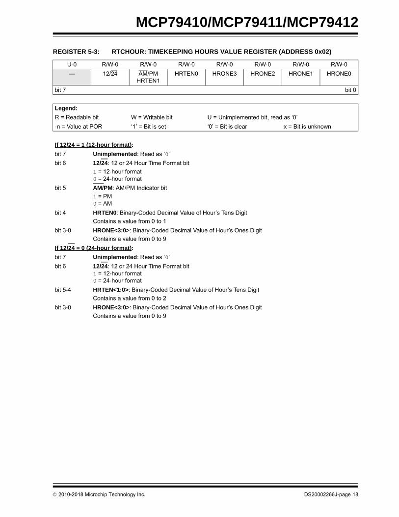
REGISTER 5-3: RTCHOUR: TIMEKEEPING HOURS VALUE REGISTER (ADDRESS 0x02)
U-0 R/W-0 R/W-0 R/W-0 R/W-0 R/W-0 R/W-0 R/W-0
— 12/24 AM/PMHRTEN1
HRTEN0 HRONE3 HRONE2 HRONE1 HRONE0
bit 7 bit 0
Legend:
R = Readable bit W = Writable bit U = Unimplemented bit, read as ‘0’
-n = Value at POR ‘1’ = Bit is set ‘0’ = Bit is clear x = Bit is unknown
If 12/24 = 1 (12-hour format):
bit 7 Unimplemented: Read as ‘0’
bit 6 12/24: 12 or 24 Hour Time Format bit
1 = 12-hour format0 = 24-hour format
bit 5 AM/PM: AM/PM Indicator bit
1 = PM0 = AM
bit 4 HRTEN0: Binary-Coded Decimal Value of Hour’s Tens Digit
Contains a value from 0 to 1
bit 3-0 HRONE<3:0>: Binary-Coded Decimal Value of Hour’s Ones Digit
Contains a value from 0 to 9
If 12/24 = 0 (24-hour format):
bit 7 Unimplemented: Read as ‘0’
bit 6 12/24: 12 or 24 Hour Time Format bit1 = 12-hour format0 = 24-hour format
bit 5-4 HRTEN<1:0>: Binary-Coded Decimal Value of Hour’s Tens Digit
Contains a value from 0 to 2
bit 3-0 HRONE<3:0>: Binary-Coded Decimal Value of Hour’s Ones Digit
Contains a value from 0 to 9
2010-2018 Microchip Technology Inc. DS20002266J-page 18
MCP79410/MCP79411/MCP79412
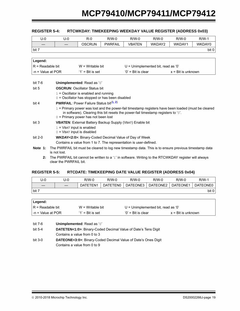
REGISTER 5-4: RTCWKDAY: TIMEKEEPING WEEKDAY VALUE REGISTER (ADDRESS 0x03)
U-0 U-0 R-0 R/W-0 R/W-0 R/W-0 R/W-0 R/W-1
— — OSCRUN PWRFAIL VBATEN WKDAY2 WKDAY1 WKDAY0
bit 7 bit 0
Legend:
R = Readable bit W = Writable bit U = Unimplemented bit, read as ‘0’
-n = Value at POR ‘1’ = Bit is set ‘0’ = Bit is clear x = Bit is unknown
bit 7-6 Unimplemented: Read as ‘0’
bit 5 OSCRUN: Oscillator Status bit
1 = Oscillator is enabled and running0 = Oscillator has stopped or has been disabled
bit 4 PWRFAIL: Power Failure Status bit(1, 2)
1 = Primary power was lost and the power-fail timestamp registers have been loaded (must be clearedin software). Clearing this bit resets the power-fail timestamp registers to ‘0’.
0 = Primary power has not been lost
bit 3 VBATEN: External Battery Backup Supply (VBAT) Enable bit
1 = VBAT input is enabled0 = VBAT input is disabled
bit 2-0 WKDAY<2:0>: Binary-Coded Decimal Value of Day of Week
Contains a value from 1 to 7. The representation is user-defined.
Note 1: The PWRFAIL bit must be cleared to log new timestamp data. This is to ensure previous timestamp data is not lost.
2: The PWRFAIL bit cannot be written to a ‘1’ in software. Writing to the RTCWKDAY register will always clear the PWRFAIL bit.
REGISTER 5-5: RTCDATE: TIMEKEEPING DATE VALUE REGISTER (ADDRESS 0x04)
Legend: — = unimplemented location, read as ‘0’. Shaded cells are not used in timekeeping.
2010-2018 Microchip Technology Inc. DS20002266J-page 20
MCP79410/MCP79411/MCP79412
5.4 Alarms
The MCP7941X features two independent alarms. Eachalarm can be used to either generate an interrupt at aspecific time in the future, or to generate a periodicinterrupt every minute, hour, day, day of week, or month.
There is a separate interrupt flag, ALMxIF, for each alarm.The interrupt flags are set by hardware when the chosenalarm mask condition matches (Table 5-5). The interruptflags must be cleared in software.
If either alarm module is enabled by setting thecorresponding ALMxEN bit in the CONTROL register, andif the square wave clock output is disabled (SQWEN = 0),then the MFP will operate in Alarm Interrupt Output mode.Refer to Section 5.5 “Output Configurations” fordetails. The alarm interrupt output is available whileoperating from the backup power supply.
Both Alarm0 and Alarm1 offer identical operation. All timeand date values are stored in the registers asbinary-coded decimal (BCD) values.
TABLE 5-5: ALARM MASKS
FIGURE 5-6: ALARM BLOCK DIAGRAM
Note: Throughout this section, references to theregister and bit names for the alarmmodules are referred to generically by theuse of ‘x’ in place of the specific modulenumber. Thus, “ALMxSEC” might refer tothe seconds register for Alarm0 or Alarm1.
ALMxMSK<2:0> Alarm Asserts on Match of
000 Seconds
001 Minutes
010 Hours
011 Day of Week
100 Date
101 Reserved
110 Reserved
111 Seconds, Minutes, Hours, Day of Week, Date, and Month
Note 1: The alarm interrupt flags must be clearedby the user. If a flag is cleared while thecorresponding alarm condition stillmatches, the flag will be set again,generating another interrupt.
2: Loading invalid values into the alarmregisters will result in undefinedoperation.
MFP
RTCSEC
RTCMIN
RTCHOUR
RTCWKDAY
RTCDATE
RTCMTH
TimekeepingRegisters
ALM1SEC
ALM1MIN
ALM1HOUR
ALM1WKDAY
ALM1DATE
ALM1MTH
Alarm1Registers
ALM0SEC
ALM0MIN
ALM0HOUR
ALM0WKDAY
ALM0DATE
ALM0MTH
Alarm0Registers
Alarm0 Mask Alarm1 MaskComparator Comparator
MFP Output Logic
SetALM0IF
SetALM1IF
ALM0MSK<2:0> ALM1MSK<2:0>
2010-2018 Microchip Technology Inc. DS20002266J-page 21
MCP79410/MCP79411/MCP79412
5.4.1 CONFIGURING THE ALARM
In order to configure the alarm modules, the followingsteps need to be performed:
1. Load the timekeeping registers and enable theoscillator
2. Configure the ALMxMSK<2:0> bits to select thedesired alarm mask
3. Set or clear the ALMPOL bit according to thedesired output polarity
4. Ensure the ALMxIF flag is cleared
5. Based on the selected alarm mask, load thealarm match value into the appropriateregister(s)
6. Enable the alarm module by setting theALMxEN bit
REGISTER 5-8: ALMxSEC: ALARM0/1 SECONDS VALUE REGISTER (ADDRESSES 0x0A/0x11)
R = Readable bit W = Writable bit U = Unimplemented bit, read as ‘0’
-n = Value at POR ‘1’ = Bit is set ‘0’ = Bit is clear x = Bit is unknown
bit 7 ALMPOL: Alarm Interrupt Output Polarity bit
1 = Asserted output state of MFP is a logic high level0 = Asserted output state of MFP is a logic low level
bit 6-4 ALMxMSK<2:0>: Alarm Mask bits
000 = Seconds match001 = Minutes match010 = Hours match (logic takes into account 12-/24-hour operation)011 = Day of week match100 = Date match101 = Reserved; do not use110 = Reserved; do not use111 = Seconds, Minutes, Hour, Day of Week, Date and Month
bit 3 ALMxIF: Alarm Interrupt Flag bit(1,2)
1 = Alarm match occurred (must be cleared in software)0 = Alarm match did not occur
bit 2-0 WKDAY<2:0>: Binary-Coded Decimal Value of Day bits
Contains a value from 1 to 7. The representation is user-defined.
Note 1: If a match condition still exists when this bit is cleared, it will be set again automatically.
2: The ALMxIF bit cannot be written to a 1 in software. Writing to the ALMxWKDAY register will always clear the ALMxIF bit.
REGISTER 5-12: ALMxDATE: ALARM0/1 DATE VALUE REGISTER (ADDRESSES 0x0E/0x15)
CONTROL OUT SQWEN ALM1EN ALM0EN EXTOSC CRSTRIM SQWFS1 SQWFS0 27
Legend: — = unimplemented location, read as ‘0’. Shaded cells are not used by alarms.
2010-2018 Microchip Technology Inc. DS20002266J-page 25
MCP79410/MCP79411/MCP79412
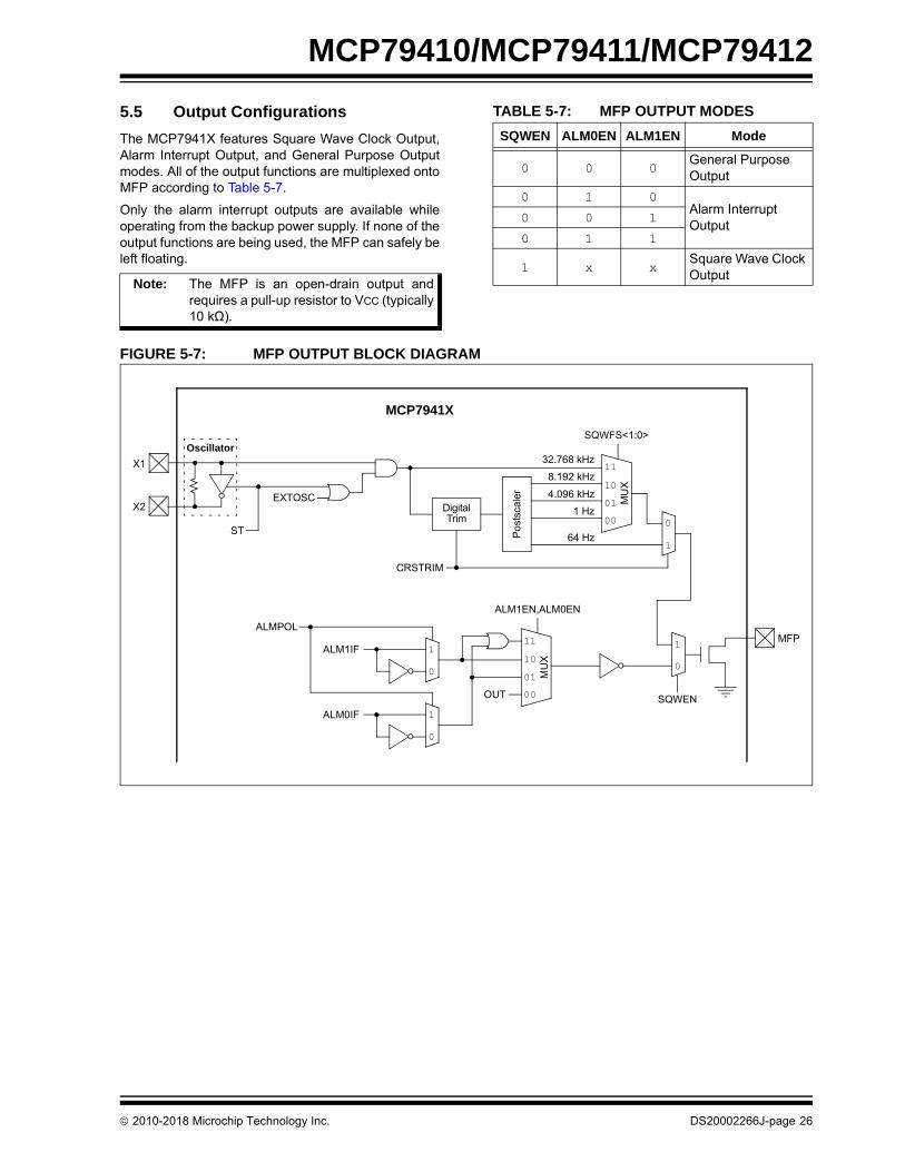
5.5 Output Configurations
The MCP7941X features Square Wave Clock Output,Alarm Interrupt Output, and General Purpose Outputmodes. All of the output functions are multiplexed ontoMFP according to Table 5-7.
Only the alarm interrupt outputs are available whileoperating from the backup power supply. If none of theoutput functions are being used, the MFP can safely beleft floating.
TABLE 5-7: MFP OUTPUT MODES
FIGURE 5-7: MFP OUTPUT BLOCK DIAGRAM
Note: The MFP is an open-drain output andrequires a pull-up resistor to VCC (typically10 kΩ).
SQWEN ALM0EN ALM1EN Mode
0 0 0 General PurposeOutput
0 1 0Alarm InterruptOutput
0 0 10 1 1
1 x x Square Wave Clock Output
X2
X1
ST
Oscillator
EXTOSC
Po
stsc
aler MU
X
32.768 kHz
8.192 kHz
4.096 kHz
1 Hz
SQWFS<1:0>
11100100
DigitalTrim
1
064 Hz
CRSTRIM
MFP
0
1
SQWEN
0
1
0
1
ALM1IF
ALM0IF
ALMPOL
MU
X
ALM1EN,ALM0EN
11100100OUT
MCP7941X
2010-2018 Microchip Technology Inc. DS20002266J-page 26
MCP79410/MCP79411/MCP79412
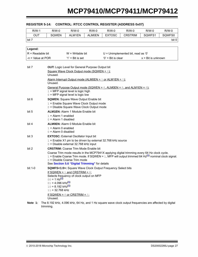
REGISTER 5-14: CONTROL: RTCC CONTROL REGISTER (ADDRESS 0x07)
R/W-1 R/W-0 R/W-0 R/W-0 R/W-0 R/W-0 R/W-0 R/W-0
OUT SQWEN ALM1EN ALM0EN EXTOSC CRSTRIM SQWFS1 SQWFS0
bit 7 bit 0
Legend:
R = Readable bit W = Writable bit U = Unimplemented bit, read as ‘0’
-n = Value at POR ‘1’ = Bit is set ‘0’ = Bit is clear x = Bit is unknown
bit 7 OUT: Logic Level for General Purpose Output bit
1 = Enable X1 pin to be driven by external 32.768 kHz source0 = Disable external 32.768 kHz input
bit 2 CRSTRIM: Coarse Trim Mode Enable bit
Coarse Trim mode results in the MCP7941X applying digital trimming every 64 Hz clock cycle.1 = Enable Coarse Trim mode. If SQWEN = 1, MFP will output trimmed 64 Hz(1) nominal clock signal.0 = Disable Coarse Trim modeSee Section 5.6 “Digital Trimming” for details
bit 1-0 SQWFS<1:0>: Square Wave Clock Output Frequency Select bits
If SQWEN = 1 and CRSTRIM = 0:Selects frequency of clock output on MFP00 = 1 Hz(1)
01 = 4.096 kHz(1)
10 = 8.192 kHz(1)
11 = 32.768 kHz
If SQWEN = 0 or CRSTRIM = 1:Unused.
Note 1: The 8.192 kHz, 4.096 kHz, 64 Hz, and 1 Hz square wave clock output frequencies are affected by digital trimming.
2010-2018 Microchip Technology Inc. DS20002266J-page 27
MCP79410/MCP79411/MCP79412
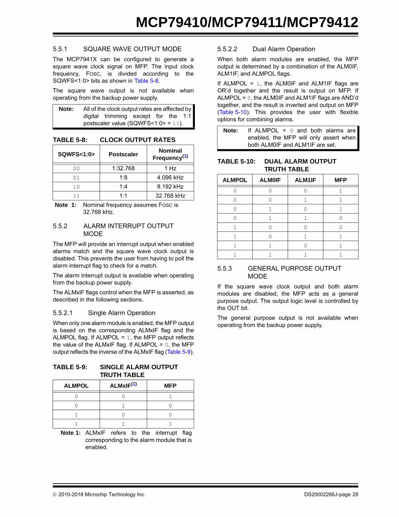
5.5.1 SQUARE WAVE OUTPUT MODE
The MCP7941X can be configured to generate asquare wave clock signal on MFP. The input clockfrequency, FOSC, is divided according to theSQWFS<1:0> bits as shown in Table 5-8.
The square wave output is not available whenoperating from the backup power supply.
TABLE 5-8: CLOCK OUTPUT RATES
5.5.2 ALARM INTERRUPT OUTPUT MODE
The MFP will provide an interrupt output when enabledalarms match and the square wave clock output isdisabled. This prevents the user from having to poll thealarm interrupt flag to check for a match.
The alarm interrupt output is available when operatingfrom the backup power supply.
The ALMxIF flags control when the MFP is asserted, asdescribed in the following sections.
5.5.2.1 Single Alarm Operation
When only one alarm module is enabled, the MFP outputis based on the corresponding ALMxIF flag and theALMPOL flag. If ALMPOL = 1, the MFP output reflectsthe value of the ALMxIF flag. If ALMPOL = 0, the MFPoutput reflects the inverse of the ALMxIF flag (Table 5-9).
TABLE 5-9: SINGLE ALARM OUTPUT TRUTH TABLE
5.5.2.2 Dual Alarm Operation
When both alarm modules are enabled, the MFPoutput is determined by a combination of the ALM0IF,ALM1IF, and ALMPOL flags.
If ALMPOL = 1, the ALM0IF and ALM1IF flags areOR’d together and the result is output on MFP. IfALMPOL = 0, the ALM0IF and ALM1IF flags are AND’dtogether, and the result is inverted and output on MFP(Table 5-10). This provides the user with flexibleoptions for combining alarms.
TABLE 5-10: DUAL ALARM OUTPUT TRUTH TABLE
5.5.3 GENERAL PURPOSE OUTPUT MODE
If the square wave clock output and both alarmmodules are disabled, the MFP acts as a generalpurpose output. The output logic level is controlled bythe OUT bit.
The general purpose output is not available whenoperating from the backup power supply.
Note: All of the clock output rates are affected bydigital trimming except for the 1:1postscaler value (SQWFS<1:0> = 11).
SQWFS<1:0> PostscalerNominal
Frequency(1)
00 1:32.768 1 Hz
01 1:8 4.096 kHz
10 1:4 8.192 kHz
11 1:1 32.768 kHz
Note 1: Nominal frequency assumes FOSC is 32.768 kHz.
ALMPOL ALMxIF(1) MFP
0 0 10 1 01 0 01 1 1
Note 1: ALMxIF refers to the interrupt flagcorresponding to the alarm module that isenabled.
Note: If ALMPOL = 0 and both alarms areenabled, the MFP will only assert whenboth ALM0IF and ALM1IF are set.
CONTROL OUT SQWEN ALM1EN ALM0EN EXTOSC CRSTRIM SQWFS1 SQWFS0 27
Legend: — = unimplemented location, read as ‘0’. Shaded cells are not used in output configuration.
2010-2018 Microchip Technology Inc. DS20002266J-page 29
MCP79410/MCP79411/MCP79412
5.6 Digital Trimming
The MCP7941X features digital trimming to correct forinaccuracies of the external crystal or clock source, upto roughly ±129 ppm when CRSTRIM = 0. In additionto compensating for intrinsic inaccuracies in the clock,this feature can also be used to correct for error due totemperature variation. This can enable the user toachieve high levels of accuracy across a widetemperature operating range.
Digital trimming consists of the MCP7941X periodicallyadding or subtracting clock cycles, resulting in smalladjustments in the internal timing. The adjustment
occurs once per minute when CRSTRIM = 0. The SIGNbit specifies whether to add cycles or to subtract them.The TRIMVAL<6:0> bits are used to specify by howmany clock cycles to adjust. Each step in theTRIMVAL<6:0> value equates to adding or subtractingtwo clock pulses to or from the 32.768 kHz clock signal.This results in a correction of roughly 1.017 ppm perstep when CRSTRIM = 0. Setting TRIMVAL<6:0> to0x00 disables digital trimming.
Digital trimming also occurs while operating off thebackup supply.
.
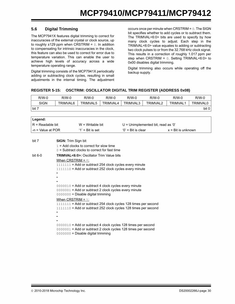
REGISTER 5-15: OSCTRIM: OSCILLATOR DIGITAL TRIM REGISTER (ADDRESS 0x08)
R = Readable bit W = Writable bit U = Unimplemented bit, read as ‘0’
-n = Value at POR ‘1’ = Bit is set ‘0’ = Bit is clear x = Bit is unknown
bit 7 SIGN: Trim Sign bit
1 = Add clocks to correct for slow time0 = Subtract clocks to correct for fast time
bit 6-0 TRIMVAL<6:0>: Oscillator Trim Value bits
When CRSTRIM = 0:1111111 = Add or subtract 254 clock cycles every minute1111110 = Add or subtract 252 clock cycles every minute•••0000010 = Add or subtract 4 clock cycles every minute0000001 = Add or subtract 2 clock cycles every minute0000000 = Disable digital trimming
When CRSTRIM = 1:1111111 = Add or subtract 254 clock cycles 128 times per second1111110 = Add or subtract 252 clock cycles 128 times per second•••0000010 = Add or subtract 4 clock cycles 128 times per second0000001 = Add or subtract 2 clock cycles 128 times per second0000000 = Disable digital trimming
2010-2018 Microchip Technology Inc. DS20002266J-page 30
MCP79410/MCP79411/MCP79412
5.6.1 CALIBRATION
In order to perform calibration, the number of errorclock pulses per minute must be found and thecorresponding trim value must be loaded intoTRIMVAL<6:0>.
There are two methods for determining the trim value.The first method involves measuring an outputfrequency directly and calculating the deviation fromideal. The second method involves observing thenumber of seconds gained or lost over a period of time.
Once the OSCTRIM register has been loaded, digitaltrimming will automatically occur every minute.
5.6.1.1 Calibration by Measuring Frequency
To calibrate the MCP7941X by measuring the outputfrequency, perform the following steps:
1. Enable the crystal oscillator or external clockinput by setting the ST bit or EXTOSC bit,respectively.
2. Ensure TRIMVAL<6:0> is reset to 0x00.
3. Select an output frequency by settingSQWFS<1:0>.
4. Set SQWEN to enable the square wave output.
5. Measure the resulting output frequency using acalibrated measurement tool, such as afrequency counter.
6. Calculate the number of error clocks per minute(see Equation 5-2).
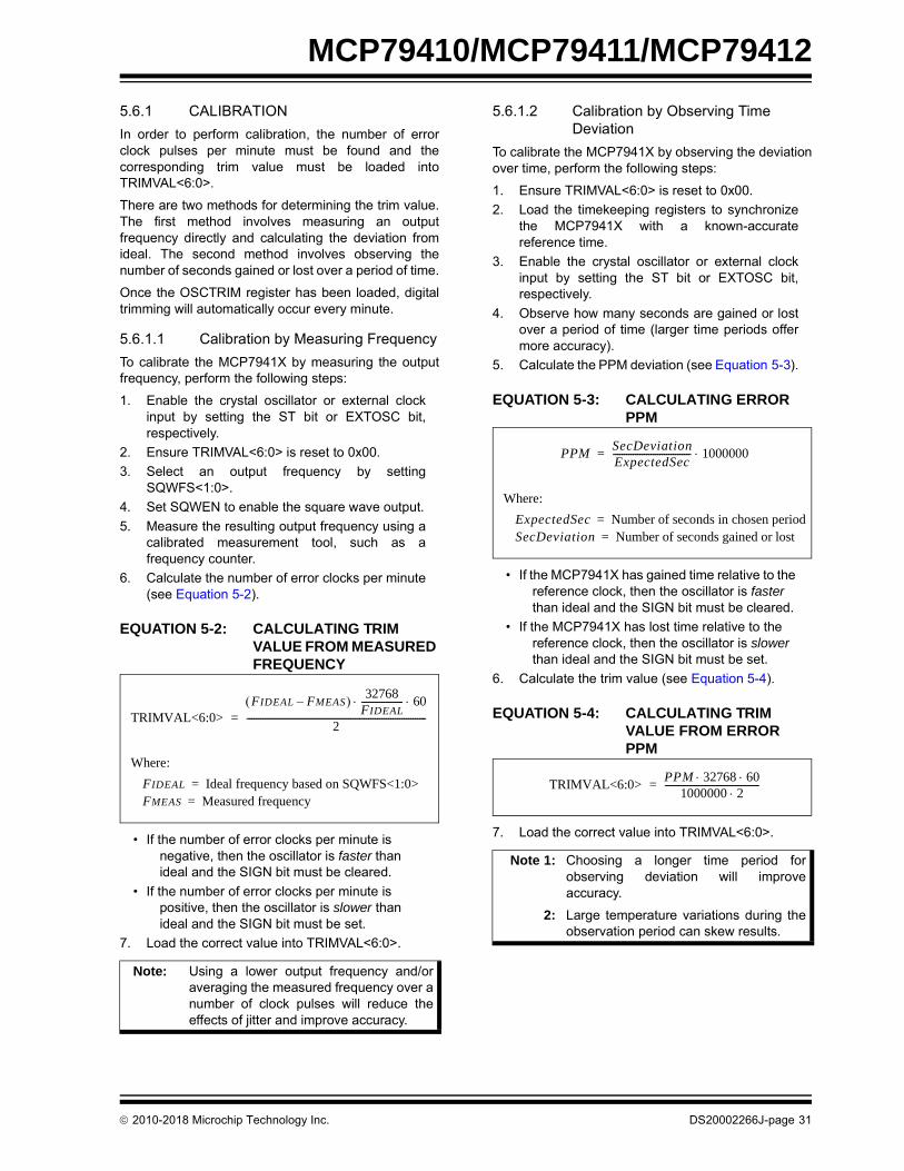
EQUATION 5-2: CALCULATING TRIM VALUE FROM MEASURED FREQUENCY
• If the number of error clocks per minute is negative, then the oscillator is faster than ideal and the SIGN bit must be cleared.
• If the number of error clocks per minute is positive, then the oscillator is slower than ideal and the SIGN bit must be set.
7. Load the correct value into TRIMVAL<6:0>.
5.6.1.2 Calibration by Observing Time Deviation
To calibrate the MCP7941X by observing the deviationover time, perform the following steps:
1. Ensure TRIMVAL<6:0> is reset to 0x00.
2. Load the timekeeping registers to synchronizethe MCP7941X with a known-accuratereference time.
3. Enable the crystal oscillator or external clockinput by setting the ST bit or EXTOSC bit,respectively.
4. Observe how many seconds are gained or lostover a period of time (larger time periods offermore accuracy).
5. Calculate the PPM deviation (see Equation 5-3).
EQUATION 5-3: CALCULATING ERROR PPM
• If the MCP7941X has gained time relative to the reference clock, then the oscillator is faster than ideal and the SIGN bit must be cleared.
• If the MCP7941X has lost time relative to the reference clock, then the oscillator is slower than ideal and the SIGN bit must be set.
6. Calculate the trim value (see Equation 5-4).
EQUATION 5-4: CALCULATING TRIM VALUE FROM ERROR PPM
7. Load the correct value into TRIMVAL<6:0>.
Note: Using a lower output frequency and/oraveraging the measured frequency over anumber of clock pulses will reduce theeffects of jitter and improve accuracy.
2010-2018 Microchip Technology Inc. DS20002266J-page 31
MCP79410/MCP79411/MCP79412
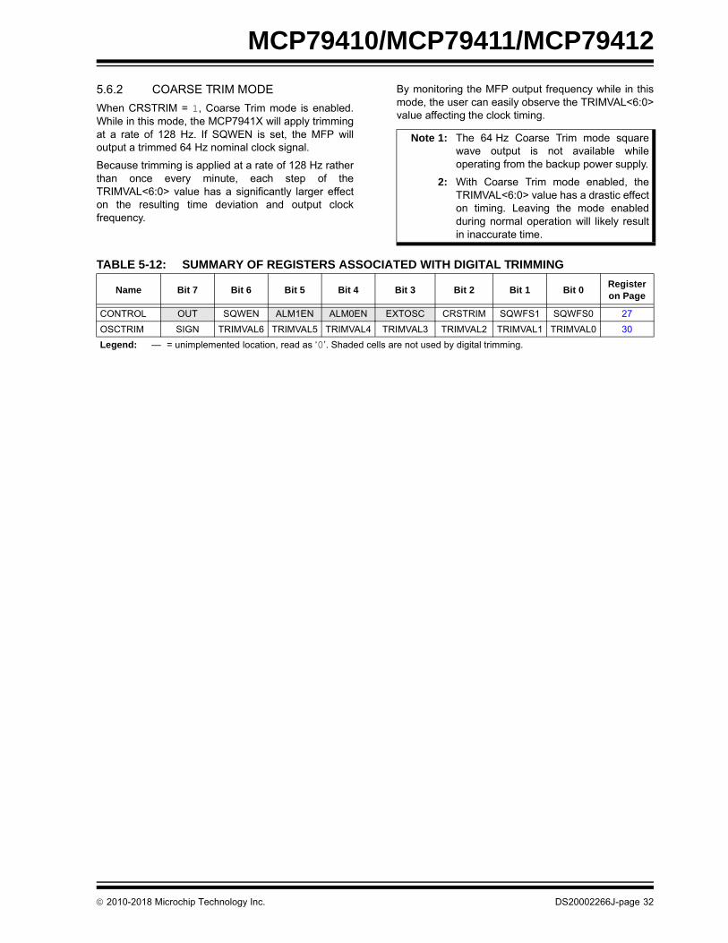
5.6.2 COARSE TRIM MODE
When CRSTRIM = 1, Coarse Trim mode is enabled.While in this mode, the MCP7941X will apply trimmingat a rate of 128 Hz. If SQWEN is set, the MFP willoutput a trimmed 64 Hz nominal clock signal.
Because trimming is applied at a rate of 128 Hz ratherthan once every minute, each step of theTRIMVAL<6:0> value has a significantly larger effecton the resulting time deviation and output clockfrequency.
By monitoring the MFP output frequency while in thismode, the user can easily observe the TRIMVAL<6:0>value affecting the clock timing.
TABLE 5-12: SUMMARY OF REGISTERS ASSOCIATED WITH DIGITAL TRIMMING
Note 1: The 64 Hz Coarse Trim mode squarewave output is not available whileoperating from the backup power supply.
2: With Coarse Trim mode enabled, theTRIMVAL<6:0> value has a drastic effecton timing. Leaving the mode enabledduring normal operation will likely resultin inaccurate time.
Name Bit 7 Bit 6 Bit 5 Bit 4 Bit 3 Bit 2 Bit 1 Bit 0Register on Page
CONTROL OUT SQWEN ALM1EN ALM0EN EXTOSC CRSTRIM SQWFS1 SQWFS0 27
Legend: — = unimplemented location, read as ‘0’. Shaded cells are not used by digital trimming.
2010-2018 Microchip Technology Inc. DS20002266J-page 32
MCP79410/MCP79411/MCP79412
5.7 Battery Backup
The MCP7941X features a backup power supply input(VBAT) that can be used to provide power to thetimekeeping circuitry, RTCC registers, and SRAM whileprimary power is unavailable. The MCP7941X willautomatically switch to backup power when VCC fallsbelow VTRIP, and back to VCC when it is above VTRIP.
The VBATEN bit must be set to enable the VBAT input.
The following functionality is maintained whileoperating on backup power:
• Timekeeping
• Alarms
• Alarm Output
• Digital Trimming
• RTCC Register and SRAM Contents
The following features are not available while operatingon backup power:
• I2C Communication
• Square Wave Clock Output
• General Purpose Output
5.7.1 POWER-FAIL TIMESTAMP
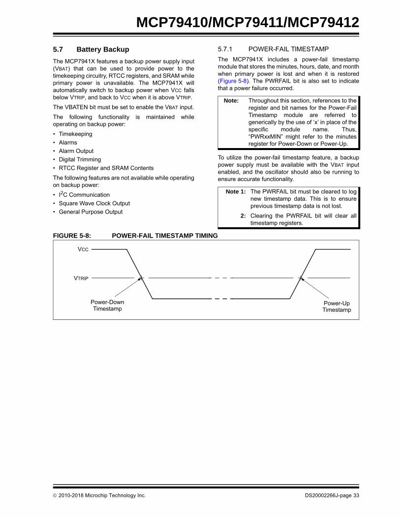
The MCP7941X includes a power-fail timestampmodule that stores the minutes, hours, date, and monthwhen primary power is lost and when it is restored(Figure 5-8). The PWRFAIL bit is also set to indicatethat a power failure occurred.
To utilize the power-fail timestamp feature, a backuppower supply must be available with the VBAT inputenabled, and the oscillator should also be running toensure accurate functionality.
FIGURE 5-8: POWER-FAIL TIMESTAMP TIMING
Note: Throughout this section, references to theregister and bit names for the Power-FailTimestamp module are referred togenerically by the use of ‘x’ in place of thespecific module name. Thus,“PWRxxMIN” might refer to the minutesregister for Power-Down or Power-Up.
Note 1: The PWRFAIL bit must be cleared to lognew timestamp data. This is to ensureprevious timestamp data is not lost.
2: Clearing the PWRFAIL bit will clear alltimestamp registers.
Power-Down Power-UpTimestamp Timestamp
VCC
VTRIP
2010-2018 Microchip Technology Inc. DS20002266J-page 33
MCP79410/MCP79411/MCP79412
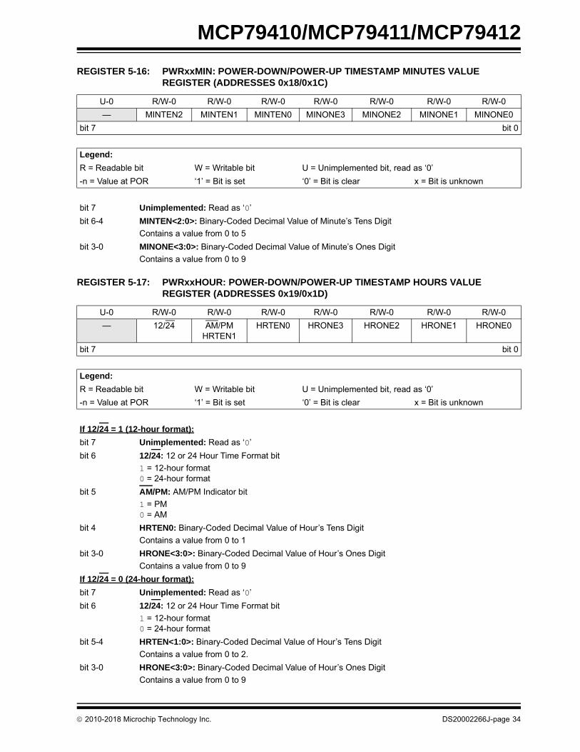
REGISTER 5-16: PWRxxMIN: POWER-DOWN/POWER-UP TIMESTAMP MINUTES VALUE REGISTER (ADDRESSES 0x18/0x1C)
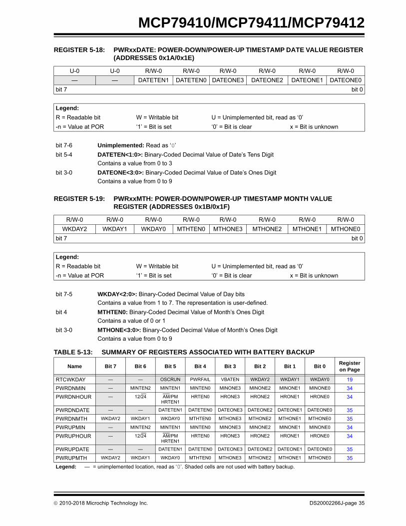
Legend: — = unimplemented location, read as ‘0’. Shaded cells are not used with battery backup.
2010-2018 Microchip Technology Inc. DS20002266J-page 35
MCP79410/MCP79411/MCP79412
6.0 ON-BOARD MEMORY
The MCP7941X has 1 Kbits (128 bytes) of EEPROM,eight bytes of protected EEPROM for storing crucialinformation, and 64 bytes of SRAM for general purposeusage. The SRAM is retained when the primary powersupply is removed if a backup supply is present andenabled. Since the EEPROM is nonvolatile, it does notrequire a supply for data retention.
Although the SRAM is a separate block from the RTCCregisters, they are accessed using the same controlbyte, ‘1101111X’. The EEPROM is in a differentaddress space and requires the use of a differentcontrol byte, ‘1010111X’. RTCC and SRAM can beaccessed for reads or writes immediately after startingan EEPROM write cycle.
6.1 SRAM/RTCC Registers
The RTCC registers are located at addresses 0x00 to0x1F, and the SRAM is located at addresses 0x20 to0x5F. The SRAM can be accessed while the RTCCregisters are being internally updated. The SRAM is notinitialized by a Power-On Reset (POR).
Neither the RTCC registers nor the SRAM can beaccessed when the device is operating off the backuppower supply.
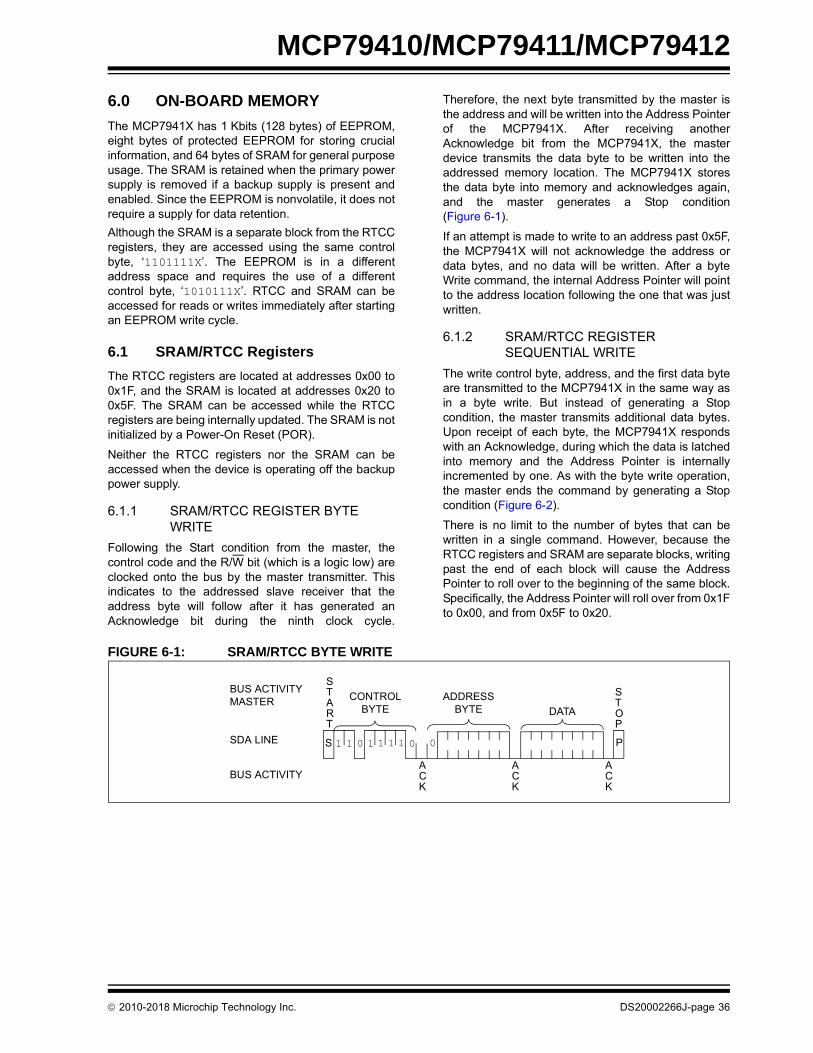
6.1.1 SRAM/RTCC REGISTER BYTE WRITE
Following the Start condition from the master, thecontrol code and the R/W bit (which is a logic low) areclocked onto the bus by the master transmitter. Thisindicates to the addressed slave receiver that theaddress byte will follow after it has generated anAcknowledge bit during the ninth clock cycle.
Therefore, the next byte transmitted by the master isthe address and will be written into the Address Pointerof the MCP7941X. After receiving anotherAcknowledge bit from the MCP7941X, the masterdevice transmits the data byte to be written into theaddressed memory location. The MCP7941X storesthe data byte into memory and acknowledges again,and the master generates a Stop condition(Figure 6-1).
If an attempt is made to write to an address past 0x5F,the MCP7941X will not acknowledge the address ordata bytes, and no data will be written. After a byteWrite command, the internal Address Pointer will pointto the address location following the one that was justwritten.
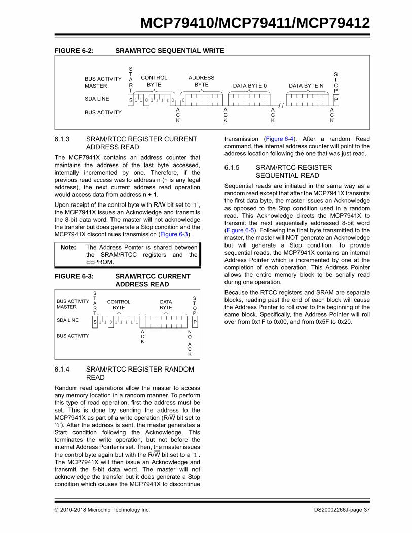
6.1.2 SRAM/RTCC REGISTER SEQUENTIAL WRITE
The write control byte, address, and the first data byteare transmitted to the MCP7941X in the same way asin a byte write. But instead of generating a Stopcondition, the master transmits additional data bytes.Upon receipt of each byte, the MCP7941X respondswith an Acknowledge, during which the data is latchedinto memory and the Address Pointer is internallyincremented by one. As with the byte write operation,the master ends the command by generating a Stopcondition (Figure 6-2).
There is no limit to the number of bytes that can bewritten in a single command. However, because theRTCC registers and SRAM are separate blocks, writingpast the end of each block will cause the AddressPointer to roll over to the beginning of the same block.Specifically, the Address Pointer will roll over from 0x1Fto 0x00, and from 0x5F to 0x20.
FIGURE 6-1: SRAM/RTCC BYTE WRITE
BUS ACTIVITYMASTER
SDA LINE
BUS ACTIVITY
START
CONTROLBYTE
ADDRESSBYTE DATA
STOP
ACK
ACK
ACK
S 1 1 0 1 01 1 1 P0
2010-2018 Microchip Technology Inc. DS20002266J-page 36
MCP79410/MCP79411/MCP79412
FIGURE 6-2: SRAM/RTCC SEQUENTIAL WRITE
6.1.3 SRAM/RTCC REGISTER CURRENT ADDRESS READ
The MCP7941X contains an address counter thatmaintains the address of the last byte accessed,internally incremented by one. Therefore, if theprevious read access was to address n (n is any legaladdress), the next current address read operationwould access data from address n + 1.
Upon receipt of the control byte with R/W bit set to ‘1’,the MCP7941X issues an Acknowledge and transmitsthe 8-bit data word. The master will not acknowledgethe transfer but does generate a Stop condition and theMCP7941X discontinues transmission (Figure 6-3).
FIGURE 6-3: SRAM/RTCC CURRENT ADDRESS READ
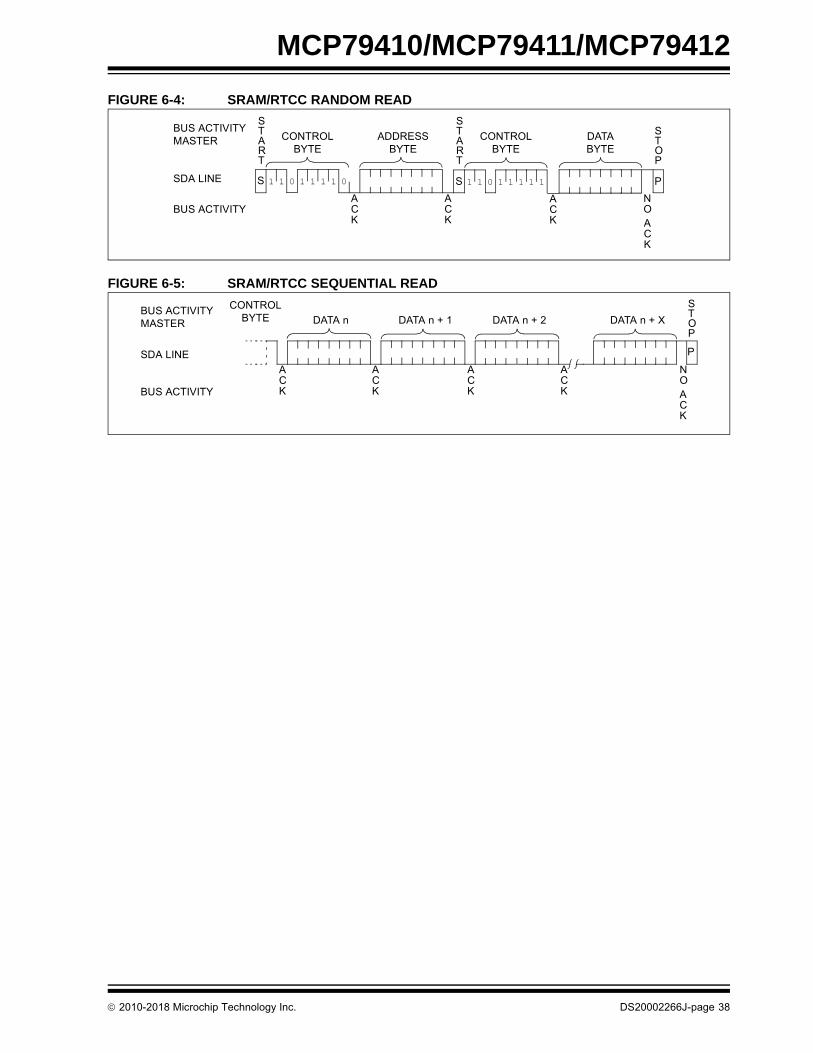
6.1.4 SRAM/RTCC REGISTER RANDOM READ
Random read operations allow the master to accessany memory location in a random manner. To performthis type of read operation, first the address must beset. This is done by sending the address to theMCP7941X as part of a write operation (R/W bit set to‘0’). After the address is sent, the master generates aStart condition following the Acknowledge. Thisterminates the write operation, but not before theinternal Address Pointer is set. Then, the master issuesthe control byte again but with the R/W bit set to a ‘1’.The MCP7941X will then issue an Acknowledge andtransmit the 8-bit data word. The master will notacknowledge the transfer but it does generate a Stopcondition which causes the MCP7941X to discontinue
transmission (Figure 6-4). After a random Readcommand, the internal address counter will point to theaddress location following the one that was just read.
6.1.5 SRAM/RTCC REGISTER SEQUENTIAL READ
Sequential reads are initiated in the same way as arandom read except that after the MCP7941X transmitsthe first data byte, the master issues an Acknowledgeas opposed to the Stop condition used in a randomread. This Acknowledge directs the MCP7941X totransmit the next sequentially addressed 8-bit word(Figure 6-5). Following the final byte transmitted to themaster, the master will NOT generate an Acknowledgebut will generate a Stop condition. To providesequential reads, the MCP7941X contains an internalAddress Pointer which is incremented by one at thecompletion of each operation. This Address Pointerallows the entire memory block to be serially readduring one operation.
Because the RTCC registers and SRAM are separateblocks, reading past the end of each block will causethe Address Pointer to roll over to the beginning of thesame block. Specifically, the Address Pointer will rollover from 0x1F to 0x00, and from 0x5F to 0x20.
BUS ACTIVITYMASTER
SDA LINE
BUS ACTIVITY
START
CONTROLBYTE
ADDRESSBYTE DATA BYTE 0
STOP
ACK
ACK
ACK
DATA BYTE N
ACK
S 1 1 0 1 01 1 1 P0
Note: The Address Pointer is shared betweenthe SRAM/RTCC registers and theEEPROM.
BUS ACTIVITYMASTER
SDA LINE
BUS ACTIVITY
PS
STOP
CONTROLBYTE
START
DATA
ACK
NO
ACK
1 01 1 1
BYTE
1 1 1
2010-2018 Microchip Technology Inc. DS20002266J-page 37
MCP79410/MCP79411/MCP79412
FIGURE 6-4: SRAM/RTCC RANDOM READ
FIGURE 6-5: SRAM/RTCC SEQUENTIAL READ
BUS ACTIVITY MASTER
SDA LINE
BUS ACTIVITYACK
NOACK
ACK
ACK
STOP
START
CONTROLBYTE
ADDRESSBYTE
CONTROLBYTE
DATABYTE
START
S 1 1 0 1 01 1 1 S 1 1 0 1 1 P1 1 1
BUS ACTIVITY MASTER
SDA LINE
BUS ACTIVITY
CONTROLBYTE DATA n DATA n + 1 DATA n + 2 DATA n + X
NOACK
ACK
ACK
ACK
ACK
STOP
P
2010-2018 Microchip Technology Inc. DS20002266J-page 38
MCP79410/MCP79411/MCP79412
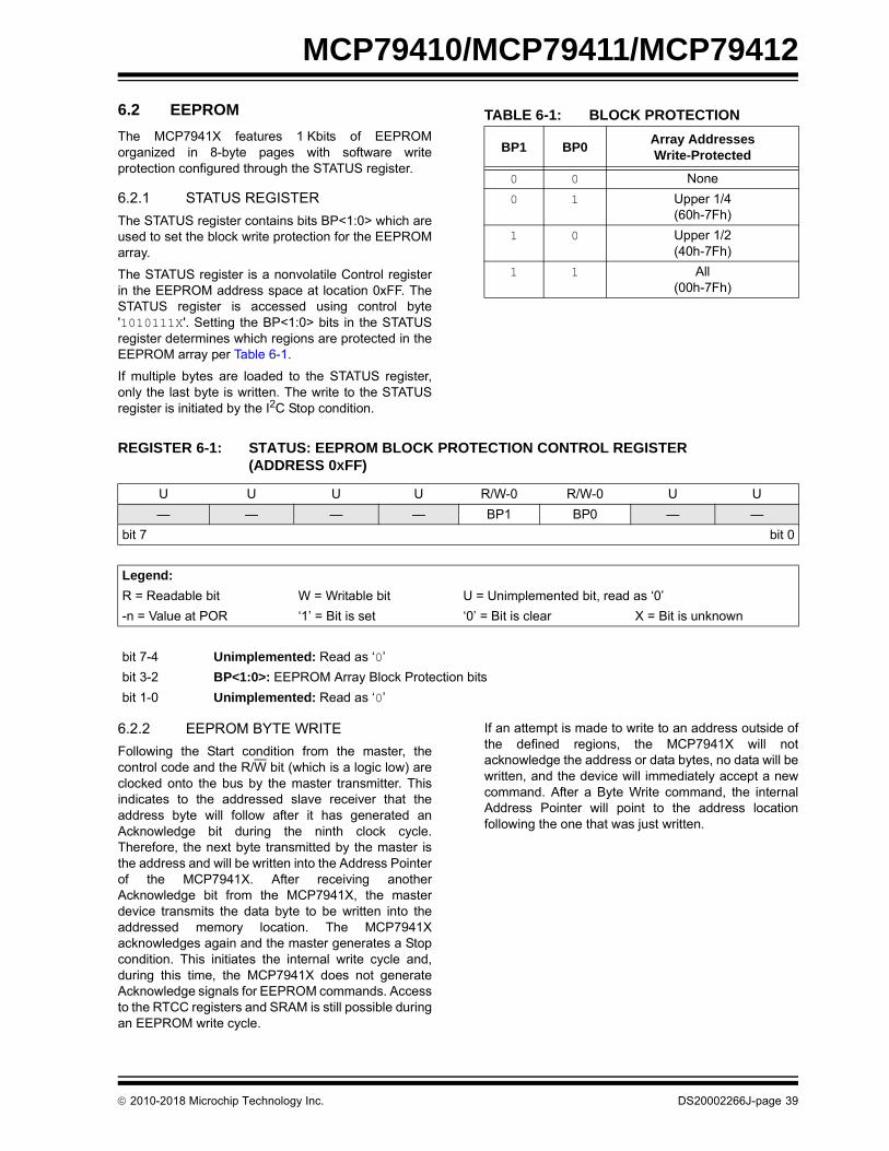
6.2 EEPROM
The MCP7941X features 1 Kbits of EEPROMorganized in 8-byte pages with software writeprotection configured through the STATUS register.
6.2.1 STATUS REGISTER
The STATUS register contains bits BP<1:0> which areused to set the block write protection for the EEPROMarray.
The STATUS register is a nonvolatile Control registerin the EEPROM address space at location 0xFF. TheSTATUS register is accessed using control byte'1010111X'. Setting the BP<1:0> bits in the STATUSregister determines which regions are protected in theEEPROM array per Table 6-1.
If multiple bytes are loaded to the STATUS register,only the last byte is written. The write to the STATUSregister is initiated by the I2C Stop condition.
6.2.2 EEPROM BYTE WRITE
Following the Start condition from the master, thecontrol code and the R/W bit (which is a logic low) areclocked onto the bus by the master transmitter. Thisindicates to the addressed slave receiver that theaddress byte will follow after it has generated anAcknowledge bit during the ninth clock cycle.Therefore, the next byte transmitted by the master isthe address and will be written into the Address Pointerof the MCP7941X. After receiving anotherAcknowledge bit from the MCP7941X, the masterdevice transmits the data byte to be written into theaddressed memory location. The MCP7941Xacknowledges again and the master generates a Stopcondition. This initiates the internal write cycle and,during this time, the MCP7941X does not generateAcknowledge signals for EEPROM commands. Accessto the RTCC registers and SRAM is still possible duringan EEPROM write cycle.
If an attempt is made to write to an address outside ofthe defined regions, the MCP7941X will notacknowledge the address or data bytes, no data will bewritten, and the device will immediately accept a newcommand. After a Byte Write command, the internalAddress Pointer will point to the address locationfollowing the one that was just written.
TABLE 6-1: BLOCK PROTECTION
BP1 BP0Array AddressesWrite-Protected
0 0 None
0 1 Upper 1/4(60h-7Fh)
1 0 Upper 1/2(40h-7Fh)
1 1 All(00h-7Fh)
REGISTER 6-1: STATUS: EEPROM BLOCK PROTECTION CONTROL REGISTER (ADDRESS 0XFF)
U U U U R/W-0 R/W-0 U U
— — — — BP1 BP0 — —
bit 7 bit 0
Legend:
R = Readable bit W = Writable bit U = Unimplemented bit, read as ‘0’
-n = Value at POR ‘1’ = Bit is set ‘0’ = Bit is clear X = Bit is unknown
bit 7-4 Unimplemented: Read as ‘0’
bit 3-2 BP<1:0>: EEPROM Array Block Protection bits
bit 1-0 Unimplemented: Read as ‘0’
2010-2018 Microchip Technology Inc. DS20002266J-page 39
MCP79410/MCP79411/MCP79412
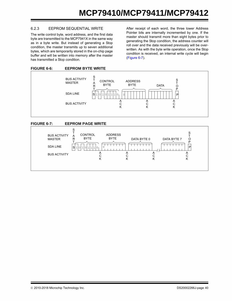
6.2.3 EEPROM SEQUENTIAL WRITE
The write control byte, word address, and the first databyte are transmitted to the MCP7941X in the same wayas in a byte write. But instead of generating a Stopcondition, the master transmits up to seven additionalbytes, which are temporarily stored in the on-chip pagebuffer and will be written into memory after the masterhas transmitted a Stop condition.
After receipt of each word, the three lower AddressPointer bits are internally incremented by one. If themaster should transmit more than eight bytes prior togenerating the Stop condition, the address counter willroll over and the data received previously will be over-written. As with the byte write operation, once the Stopcondition is received, an internal write cycle will begin(Figure 6-7).
FIGURE 6-6: EEPROM BYTE WRITE
FIGURE 6-7: EEPROM PAGE WRITE
BUS ACTIVITYMASTER
SDA LINE
BUS ACTIVITY
START
CONTROLBYTE
ADDRESS BYTE DATA
STOP
ACK
ACK
ACK
S 1 0 1 0 01 1 1 P0
BUS ACTIVITYMASTER
SDA LINE
BUS ACTIVITY
START
CONTROLBYTE
ADDRESS BYTE DATA BYTE 0
STOP
ACK
ACK
ACK
DATA BYTE 7
ACK
S 1 0 1 0 01 1 1 P0
2010-2018 Microchip Technology Inc. DS20002266J-page 40
MCP79410/MCP79411/MCP79412
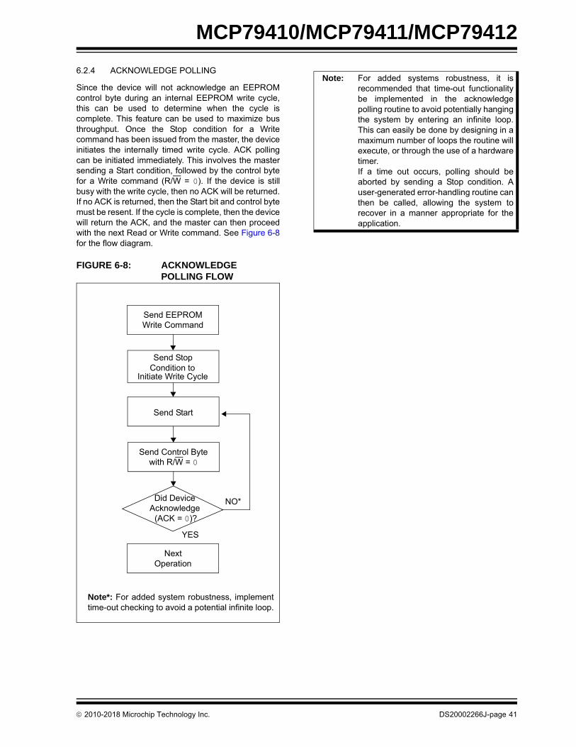
6.2.4 ACKNOWLEDGE POLLING
Since the device will not acknowledge an EEPROMcontrol byte during an internal EEPROM write cycle,this can be used to determine when the cycle iscomplete. This feature can be used to maximize busthroughput. Once the Stop condition for a Writecommand has been issued from the master, the deviceinitiates the internally timed write cycle. ACK pollingcan be initiated immediately. This involves the mastersending a Start condition, followed by the control bytefor a Write command (R/W = 0). If the device is stillbusy with the write cycle, then no ACK will be returned.If no ACK is returned, then the Start bit and control bytemust be resent. If the cycle is complete, then the devicewill return the ACK, and the master can then proceedwith the next Read or Write command. See Figure 6-8for the flow diagram.
FIGURE 6-8: ACKNOWLEDGE POLLING FLOW
Send EEPROMWrite Command
Send StopCondition to
Initiate Write Cycle
Send Start
Send Control Bytewith R/W = 0
Did DeviceAcknowledge
(ACK = 0)?
NextOperation
NO*
YES
Note*: For added system robustness, implementtime-out checking to avoid a potential infinite loop.
Note: For added systems robustness, it isrecommended that time-out functionalitybe implemented in the acknowledgepolling routine to avoid potentially hangingthe system by entering an infinite loop.This can easily be done by designing in amaximum number of loops the routine willexecute, or through the use of a hardwaretimer.If a time out occurs, polling should beaborted by sending a Stop condition. Auser-generated error-handling routine canthen be called, allowing the system torecover in a manner appropriate for theapplication.
2010-2018 Microchip Technology Inc. DS20002266J-page 41
MCP79410/MCP79411/MCP79412
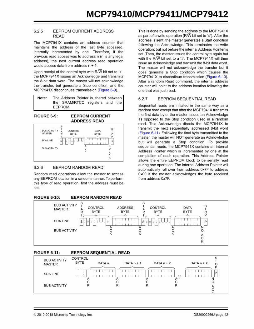
6.2.5 EEPROM CURRENT ADDRESS READ
The MCP7941X contains an address counter thatmaintains the address of the last byte accessed,internally incremented by one. Therefore, if theprevious read access was to address n (n is any legaladdress), the next current address read operationwould access data from address n + 1.
Upon receipt of the control byte with R/W bit set to ‘1’,the MCP7941X issues an Acknowledge and transmitsthe 8-bit data word. The master will not acknowledgethe transfer, but generate a Stop condition, and theMCP7941X discontinues transmission (Figure 6-9).
FIGURE 6-9: EEPROM CURRENT ADDRESS READ
6.2.6 EEPROM RANDOM READ
Random read operations allow the master to accessany EEPROM location in a random manner. To performthis type of read operation, first the address must beset.
This is done by sending the address to the MCP7941Xas part of a write operation (R/W bit set to ‘0’). After theaddress is sent, the master generates a Start conditionfollowing the Acknowledge. This terminates the writeoperation, but not before the internal Address Pointer isset. Then, the master issues the control byte again butwith the R/W bit set to a ‘1’. The MCP7941X will thenissue an Acknowledge and transmit the 8-bit data word.The master will not acknowledge the transfer but itdoes generate a Stop condition which causes theMCP7941X to discontinue transmission (Figure 6-10).After a random Read command, the internal addresscounter will point to the address location following theone that was just read.
6.2.7 EEPROM SEQUENTIAL READ
Sequential reads are initiated in the same way as arandom read except that after the MCP7941X transmitsthe first data byte, the master issues an Acknowledgeas opposed to the Stop condition used in a randomread. This Acknowledge directs the MCP7941X totransmit the next sequentially addressed 8-bit word(Figure 6-11). Following the final byte transmitted to themaster, the master will NOT generate an Acknowledgebut will generate a Stop condition. To providesequential reads, the MCP7941X contains an internalAddress Pointer which is incremented by one at thecompletion of each operation. This Address Pointerallows the entire EEPROM block to be serially readduring one operation. The internal Address Pointer willautomatically roll over from address 0x7F to address0x00 if the master acknowledges the byte receivedfrom address 0x7F.
FIGURE 6-10: EEPROM RANDOM READ
FIGURE 6-11: EEPROM SEQUENTIAL READ
Note: The Address Pointer is shared betweenthe SRAM/RTCC registers and theEEPROM.
BUS ACTIVITYMASTER
SDA LINE
BUS ACTIVITY
PS
STOP
CONTROLBYTE
START
DATA
ACK
NO
ACK
1 10 0 1
BYTE
1 1 1
BUS ACTIVITY MASTER
SDA LINE
BUS ACTIVITYACK
NOACK
ACK
ACK
STOP
START
CONTROLBYTE
ADDRESSBYTE
CONTROLBYTE
DATABYTE
START
S 1 0 1 0 01 1 1 S 1 0 1 0 1 P1 1 1
BUS ACTIVITY MASTER
SDA LINE
BUS ACTIVITY
CONTROLBYTE DATA n DATA n + 1 DATA n + 2 DATA n + X
NOACK
ACK
ACK
ACK
ACK
STOP
P
2010-2018 Microchip Technology Inc. DS20002266J-page 42
MCP79410/MCP79411/MCP79412
6.3 Protected EEPROM
The MCP7941X features a 64-bit protected EEPROMblock that requires a special unlock sequence to befollowed in order to write to the memory. Note thatreading from the memory does not require the unlocksequence to be performed. The protected EEPROMcan be used for storing crucial information such as aunique serial number. The MCP79411 and MCP79412include an EUI-48 and EUI-64 node address,respectively, preprogrammed into the protectedEEPROM block. Custom programming is alsoavailable.
The protected EEPROM block is located at addresses0xF0 to 0xF7 and is accessed using the ‘1010111X’control byte.
6.3.1 PROTECTED EEPROM UNLOCK SEQUENCE
The protected EEPROM block requires a specialunlock sequence to prevent unintended writes, utilizingthe EEUNLOCK register. The EEUNLOCK register isnot a physical register; it is used exclusively in theEEPROM write sequence. Reading from EEUNLOCKwill read all 0’s.
To unlock the block, the following sequence must befollowed:
1. Write 0x55 to the EEUNLOCK register
2. Write 0xAA to the EEUNLOCK register
3. Write the desired data bytes to the EEPROM
Figure 6-12 illustrates the sequence.
The entire EEPROM block does not have to be writtenin a single operation. However, the block is locked aftereach write operation and must be unlocked again tostart a new Write command.
FIGURE 6-12: PROTECTED EEPROM UNLOCK AND SEQUENTIAL WRITE
Note: Attempts to access invalid addresses(Figure 5-1) will result in the MCP7941Xnot acknowledging the address.
Note 1: Diverging from any step of the unlocksequence may result in the EEPROMremaining locked and the write operationbeing ignored.
2: Unlocking the EEPROM is not required inorder to read from the memory.
BUS ACTIVITYMASTER
SDA LINE
BUS ACTIVITY
START
CONTROLBYTE
ADDRESSBYTE DATA
STOP
ACK
ACK
ACK
S 1 1 0 1 01 P0
BUS ACTIVITYMASTER
SDA LINE
BUS ACTIVITY
START
CONTROLBYTE
ADDRESSBYTE DATA BYTE 0
STOP
ACK
ACK
ACK
DATA BYTE n
ACK
S 1 0 1 0 0 P1
0 0 0 1 0 0 1 0 1 0 1 0 1 0 1
BUS ACTIVITYMASTER
SDA LINE
BUS ACTIVITY
START
CONTROLBYTE
ADDRESSBYTE DATA
STOP
ACK
ACK
ACK
S 1 1 0 1 01 P0 0 0 0 1 0 0 1 1 0 1 0 1 0 1 0
1 1 1 01 1 1
1 1
1 1
1. Write 0x55 toEEUNLOCK
2. Write 0xAA toEEUNLOCK
3. Write Data toEEPROM
Register
Register
2010-2018 Microchip Technology Inc. DS20002266J-page 43
MCP79410/MCP79411/MCP79412
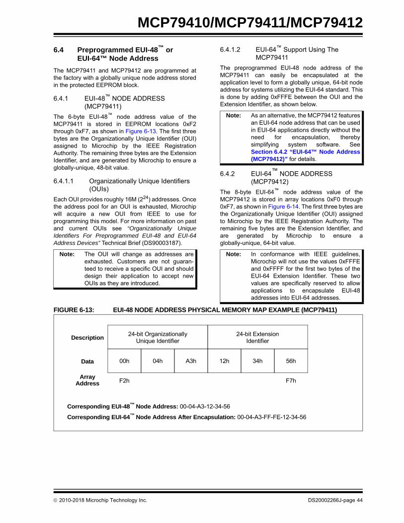
6.4 Preprogrammed EUI-48™ or EUI-64™ Node Address
The MCP79411 and MCP79412 are programmed atthe factory with a globally unique node address storedin the protected EEPROM block.
6.4.1 EUI-48™ NODE ADDRESS (MCP79411)
The 6-byte EUI-48™ node address value of theMCP79411 is stored in EEPROM locations 0xF2through 0xF7, as shown in Figure 6-13. The first threebytes are the Organizationally Unique Identifier (OUI)assigned to Microchip by the IEEE RegistrationAuthority. The remaining three bytes are the ExtensionIdentifier, and are generated by Microchip to ensure aglobally-unique, 48-bit value.
Each OUI provides roughly 16M (224) addresses. Oncethe address pool for an OUI is exhausted, Microchipwill acquire a new OUI from IEEE to use forprogramming this model. For more information on pastand current OUIs see “Organizationally UniqueIdentifiers For Preprogrammed EUI-48 and EUI-64Address Devices” Technical Brief (DS90003187).
6.4.1.2 EUI-64™ Support Using The MCP79411
The preprogrammed EUI-48 node address of theMCP79411 can easily be encapsulated at theapplication level to form a globally unique, 64-bit nodeaddress for systems utilizing the EUI-64 standard. Thisis done by adding 0xFFFE between the OUI and theExtension Identifier, as shown below.
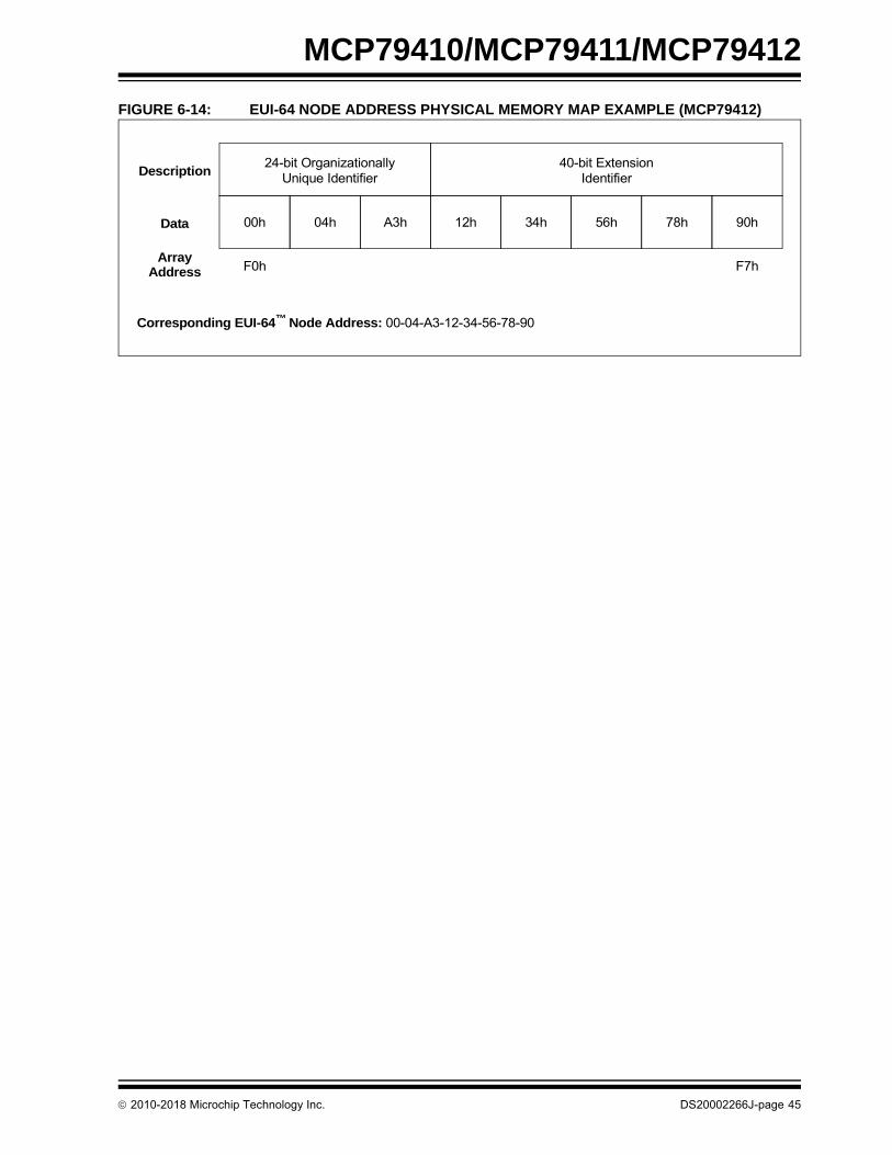
6.4.2 EUI-64™ NODE ADDRESS (MCP79412)
The 8-byte EUI-64™ node address value of theMCP79412 is stored in array locations 0xF0 through0xF7, as shown in Figure 6-14. The first three bytes arethe Organizationally Unique Identifier (OUI) assignedto Microchip by the IEEE Registration Authority. Theremaining five bytes are the Extension Identifier, andare generated by Microchip to ensure aglobally-unique, 64-bit value.
FIGURE 6-13: EUI-48 NODE ADDRESS PHYSICAL MEMORY MAP EXAMPLE (MCP79411)
Note: The OUI will change as addresses areexhausted. Customers are not guaran-teed to receive a specific OUI and shoulddesign their application to accept newOUIs as they are introduced.
Note: As an alternative, the MCP79412 featuresan EUI-64 node address that can be usedin EUI-64 applications directly without theneed for encapsulation, therebysimplifying system software. SeeSection 6.4.2 “EUI-64™ Node Address(MCP79412)” for details.
Note: In conformance with IEEE guidelines,Microchip will not use the values 0xFFFEand 0xFFFF for the first two bytes of theEUI-64 Extension Identifier. These twovalues are specifically reserved to allowapplications to encapsulate EUI-48addresses into EUI-64 addresses.
2010-2018 Microchip Technology Inc. DS20002266J-page 45
MCP79410/MCP79411/MCP79412
7.0 PACKAGING INFORMATION
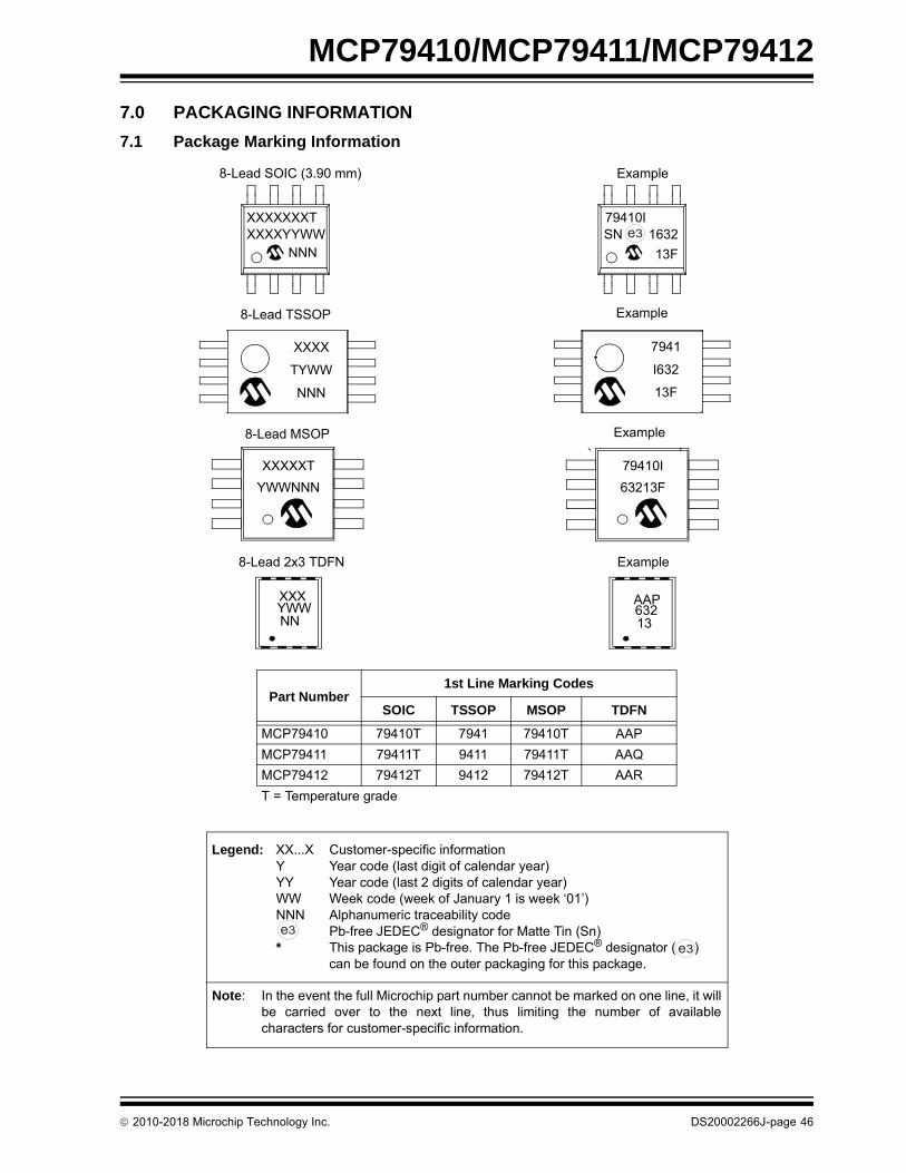
7.1 Package Marking Information
8-Lead SOIC (3.90 mm) Example
XXXXXXXTXXXXYYWW
NNN
8-Lead TSSOP Example
79410ISN 1632
13F
8-Lead MSOP Example
XXXX
TYWW
NNN
XXXXXT
YWWNNN
7941
I632
13F
79410I
63213F
3e
8-Lead 2x3 TDFN
XXXYWWNN
AAP63213
Example
Part Number1st Line Marking Codes
SOIC TSSOP MSOP TDFN
MCP79410 79410T 7941 79410T AAP
MCP79411 79411T 9411 79411T AAQ
MCP79412 79412T 9412 79412T AAR
T = Temperature grade
Legend: XX...X Customer-specific informationY Year code (last digit of calendar year)YY Year code (last 2 digits of calendar year)WW Week code (week of January 1 is week ‘01’)NNN Alphanumeric traceability code Pb-free JEDEC® designator for Matte Tin (Sn)* This package is Pb-free. The Pb-free JEDEC® designator ( )
can be found on the outer packaging for this package.
Note: In the event the full Microchip part number cannot be marked on one line, it willbe carried over to the next line, thus limiting the number of availablecharacters for customer-specific information.
3e
3e
2010-2018 Microchip Technology Inc. DS20002266J-page 46
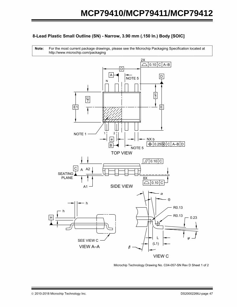
MCP79410/MCP79411/MCP79412
0.25 C A–B D
CSEATING
PLANE
TOP VIEW
SIDE VIEW
VIEW A–A
0.10 C
0.10 C
Microchip Technology Drawing No. C04-057-SN Rev D Sheet 1 of 2
8X
For the most current package drawings, please see the Microchip Packaging Specification located athttp://www.microchip.com/packaging
Note:
8-Lead Plastic Small Outline (SN) - Narrow, 3.90 mm (.150 In.) Body [SOIC]
1 2
N
h
h
A1
A2A
A
B
e
D
E
E2
E12
E1
NOTE 5
NOTE 5
NX b
0.10 C A–B2X
H 0.23
(L1)L
R0.13
R0.13
VIEW C
SEE VIEW C
NOTE 1
D
2010-2018 Microchip Technology Inc. DS20002266J-page 47
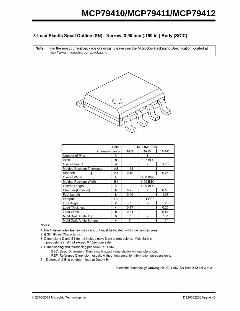
MCP79410/MCP79411/MCP79412
Microchip Technology Drawing No. C04-057-SN Rev D Sheet 2 of 2
8-Lead Plastic Small Outline (SN) - Narrow, 3.90 mm (.150 In.) Body [SOIC]
For the most current package drawings, please see the Microchip Packaging Specification located athttp://www.microchip.com/packaging
protrusions shall not exceed 0.15mm per side.3. Dimensions D and E1 do not include mold flash or protrusions. Mold flash or
REF: Reference Dimension, usually without tolerance, for information purposes only.BSC: Basic Dimension. Theoretically exact value shown without tolerances.
1. Pin 1 visual index feature may vary, but must be located within the hatched area.2. § Significant Characteristic
4. Dimensioning and tolerancing per ASME Y14.5M
Notes:
§
Footprint L1 1.04 REF
5. Datums A & B to be determined at Datum H.
2010-2018 Microchip Technology Inc. DS20002266J-page 48
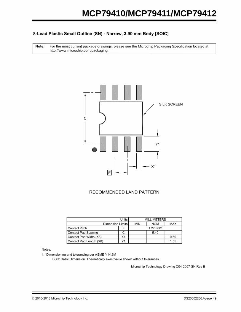
MCP79410/MCP79411/MCP79412
RECOMMENDED LAND PATTERN
Microchip Technology Drawing C04-2057-SN Rev B
8-Lead Plastic Small Outline (SN) - Narrow, 3.90 mm Body [SOIC]
BSC: Basic Dimension. Theoretically exact value shown without tolerances.
Notes:Dimensioning and tolerancing per ASME Y14.5M1.
For the most current package drawings, please see the Microchip Packaging Specification located athttp://www.microchip.com/packaging
Note:
Dimension LimitsUnits
CContact Pad SpacingContact Pitch
MILLIMETERS
1.27 BSCMIN
EMAX
5.40
Contact Pad Length (X8)Contact Pad Width (X8)
Y1X1
1.550.60
NOM
E
X1
C
Y1
SILK SCREEN
2010-2018 Microchip Technology Inc. DS20002266J-page 49
2010-2018 Microchip Technology Inc. DS20002266J-page 50
MCP79410/MCP79411/MCP79412
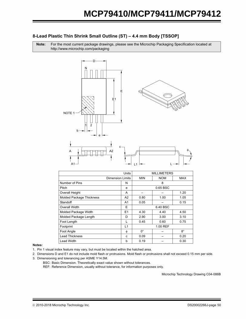
Note: For the most current package drawings, please see the Microchip Packaging Specification located at http://www.microchip.com/packaging
2010-2018 Microchip Technology Inc. DS20002266J-page 51
MCP79410/MCP79411/MCP79412
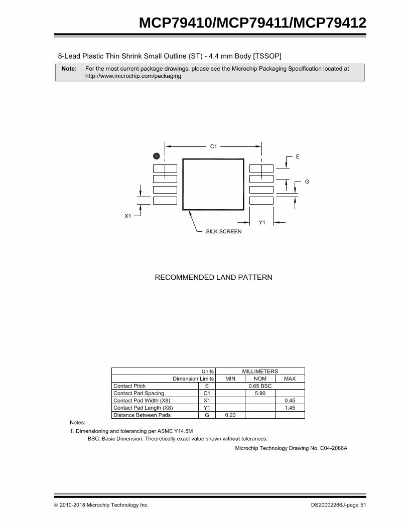
Note: For the most current package drawings, please see the Microchip Packaging Specification located at http://www.microchip.com/packaging
2010-2018 Microchip Technology Inc. DS20002266J-page 52
MCP79410/MCP79411/MCP79412
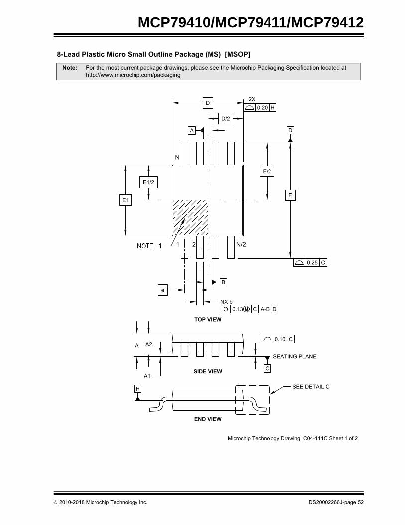
Note: For the most current package drawings, please see the Microchip Packaging Specification located at http://www.microchip.com/packaging
2010-2018 Microchip Technology Inc. DS20002266J-page 53
MCP79410/MCP79411/MCP79412
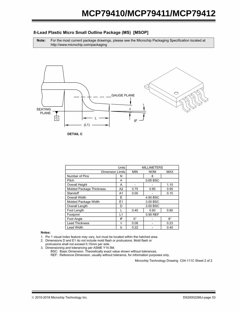
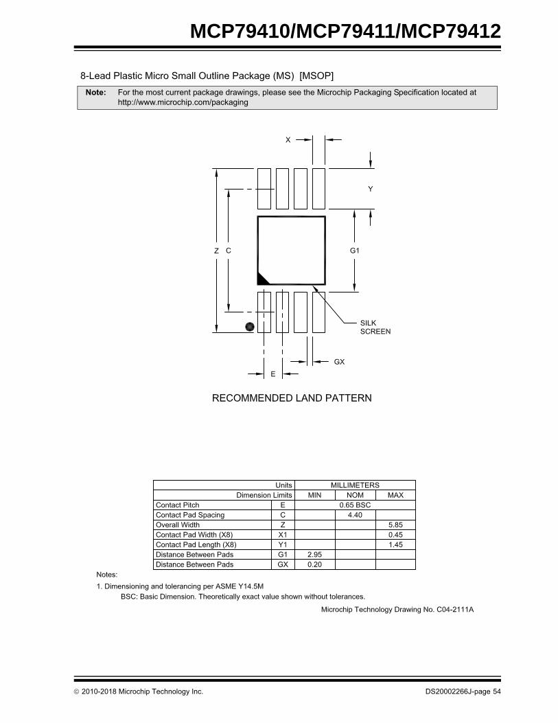
Note: For the most current package drawings, please see the Microchip Packaging Specification located at http://www.microchip.com/packaging
2010-2018 Microchip Technology Inc. DS20002266J-page 54
MCP79410/MCP79411/MCP79412
BA
0.15 C
0.15 C
0.10 C A B0.05 C
(DATUM B)(DATUM A)
CSEATING
PLANE
NOTE 1
1 2
N
2X
TOP VIEW
SIDE VIEW
BOTTOM VIEW
NOTE 1
1 2
N
0.10 C A B
0.10 C A B
0.10 C
0.08 C
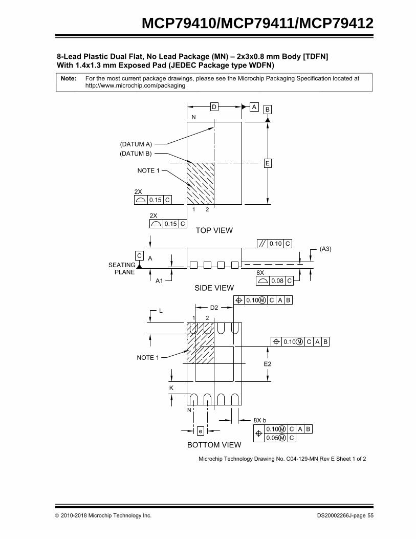
Microchip Technology Drawing No. C04-129-MN Rev E Sheet 1 of 2
2X
8X
For the most current package drawings, please see the Microchip Packaging Specification located athttp://www.microchip.com/packaging
Note:
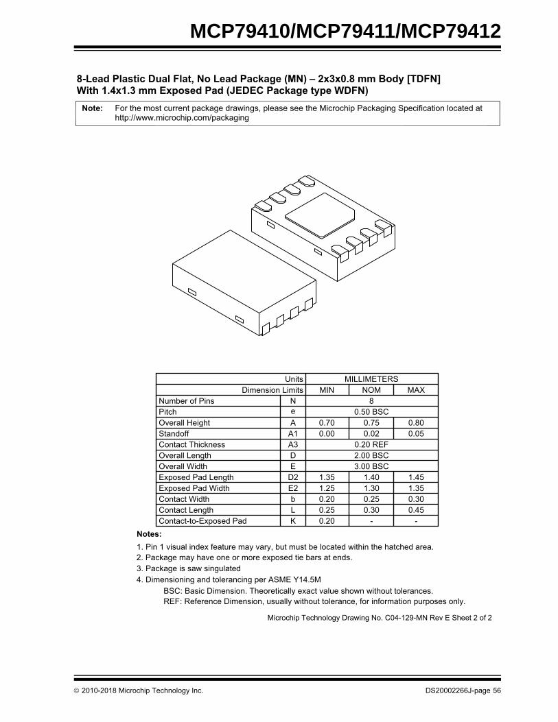
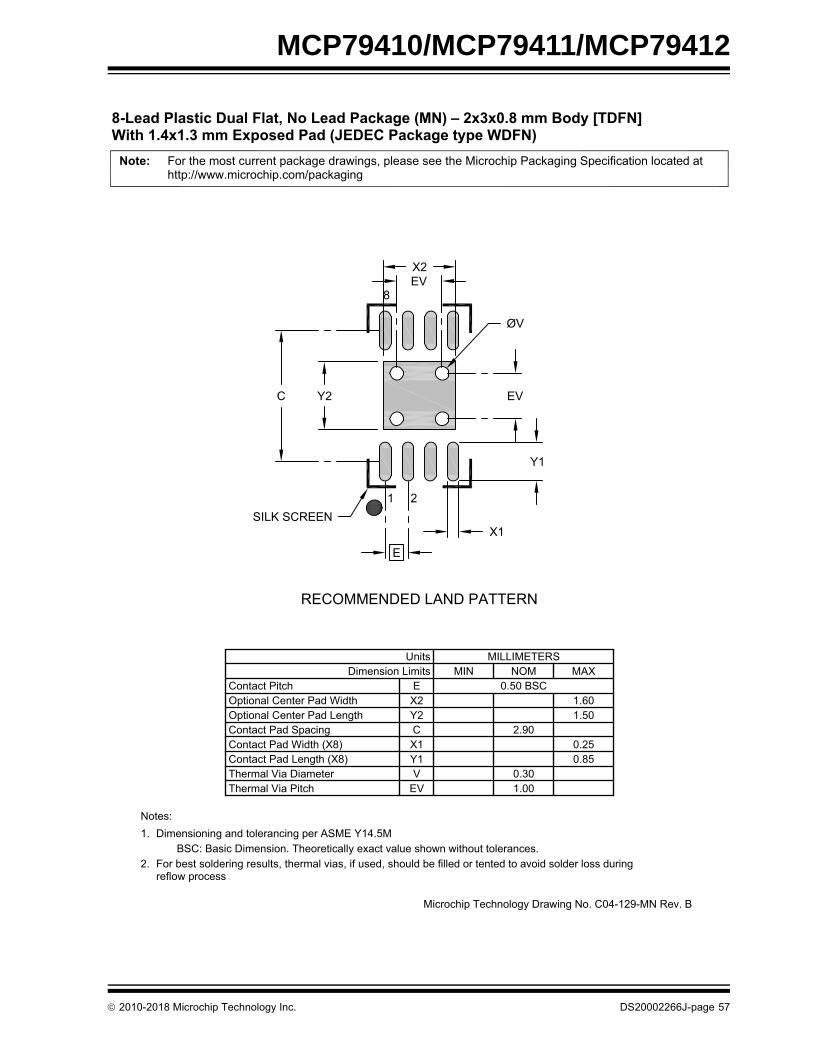
8-Lead Plastic Dual Flat, No Lead Package (MN) – 2x3x0.8 mm Body [TDFN]
D
E
D2
E2
A(A3)
A1
e
8X b
L
K
With 1.4x1.3 mm Exposed Pad (JEDEC Package type WDFN)
2010-2018 Microchip Technology Inc. DS20002266J-page 55
MCP79410/MCP79411/MCP79412
Microchip Technology Drawing No. C04-129-MN Rev E Sheet 2 of 2
8-Lead Plastic Dual Flat, No Lead Package (MN) – 2x3x0.8 mm Body [TDFN]
For the most current package drawings, please see the Microchip Packaging Specification located athttp://www.microchip.com/packaging
Note:
NOMMILLIMETERS
0.50 BSC
2.00 BSC3.00 BSC
0.20 REF
1. Pin 1 visual index feature may vary, but must be located within the hatched area.
BSC: Basic Dimension. Theoretically exact value shown without tolerances.REF: Reference Dimension, usually without tolerance, for information purposes only.
Contact-to-Exposed Pad
Contact Thickness
Exposed Pad WidthExposed Pad Length
4. Dimensioning and tolerancing per ASME Y14.5M3. Package is saw singulated2. Package may have one or more exposed tie bars at ends.
Notes:
Contact Width
Overall WidthOverall Length
Contact Length
Standoff
Number of Pins
Overall HeightPitch
K 0.20
Units
NeA
Dimension Limits
DA3A1
b
D2E2
E
L0.20
1.351.25
0.25
0.000.70
MIN
--
0.250.30
1.301.40
1.350.300.45
1.45
8
0.750.02 0.05
0.80
MAX
With 1.4x1.3 mm Exposed Pad (JEDEC Package type WDFN)
2010-2018 Microchip Technology Inc. DS20002266J-page 56
MCP79410/MCP79411/MCP79412
RECOMMENDED LAND PATTERN
Dimension LimitsUnits
Optional Center Pad WidthOptional Center Pad Length
Contact Pitch
Y2X2
1.501.60
MILLIMETERS
0.50 BSCMIN
EMAX
Contact Pad Length (X8)Contact Pad Width (X8)
Y1X1
0.850.25
Microchip Technology Drawing No. C04-129-MN Rev. B
NOM
8-Lead Plastic Dual Flat, No Lead Package (MN) – 2x3x0.8 mm Body [TDFN]
1 2
8
CContact Pad Spacing 2.90
Thermal Via Diameter VThermal Via Pitch EV
0.301.00
BSC: Basic Dimension. Theoretically exact value shown without tolerances.
Notes:Dimensioning and tolerancing per ASME Y14.5M
For best soldering results, thermal vias, if used, should be filled or tented to avoid solder loss duringreflow process
1.
2.
For the most current package drawings, please see the Microchip Packaging Specification located athttp://www.microchip.com/packaging
Note:
C
E
X1
Y1
Y2
X2EV
EV
ØV
SILK SCREEN
With 1.4x1.3 mm Exposed Pad (JEDEC Package type WDFN)
2010-2018 Microchip Technology Inc. DS20002266J-page 57
MCP79410/MCP79411/MCP79412
APPENDIX A: REVISION HISTORY
Revision A (10/2010)
Initial release of this document.
Revision B (03/2011)
Minor typographical edits; Added Appendix B: DeviceErrata.
Revised Features page; Revised Schematic, BlockDiagram; Added detailed descriptions for Registers;Minor updates to the overall content.
Revision F (03/2014)
Updated overall content for improved clarity; Addeddetailed descriptions of registers; Updated blockdiagram and application schematic; Defined names forall bits and registers, and renamed the bits shown inTable 7-1 for clarification; Renamed the DC character-istics shown in Table 7-2 for clarification.
TABLE 7-1: BIT NAME CHANGES
Old Bit Name New Bit Name
OSCON OSCRUN
VBAT PWRFAIL
LP LPYR
SQWE SQWEN
ALM0 ALM0EN
ALM1 ALM1EN
RS0 SQWFS0
RS1 SQWFS1
RS2 CRSTRIM
CALIBRATION TRIMVAL<6:0>
ALM0POL ALMPOL
ALM1POL ALMPOL
ALM0C<2:0> ALM0MSK<2:0>
ALM1C<2:0> ALM1MSK<2:0>
2010-2018 Microchip Technology Inc. DS20002266J-page 58
Operating Current EEPROM ICC Read EEPROM Operating Current ICCEERD
ICC Write ICCEEWR
Operating Current SRAM ICC Read SRAM/RTCC Register Operating Current ICCREAD
ICC Write ICCWRITE
Operating Current IVCC Timekeeping Current ICCT
IBAT Timekeeping Backup Current IBATT
Standby Current ICCS VCC Data Retention Current (oscillator off) ICCDAT
2010-2018 Microchip Technology Inc. DS20002266J-page 59
MCP79410/MCP79411/MCP79412
NOTES:
2010-2018 Microchip Technology Inc. DS20002266J-page 60
MCP79410/MCP79411/MCP79412
THE MICROCHIP WEBSITE
Microchip provides online support via our website atwww.microchip.com. This website is used as a meansto make files and information easily available tocustomers. Accessible by using your favorite Internetbrowser, the website contains the following information:
• Product Support – Data sheets and errata, appli-cation notes and sample programs, designresources, user’s guides and hardware supportdocuments, latest software releases and archivedsoftware
• General Technical Support – Frequently AskedQuestions (FAQ), technical support requests,online discussion groups, Microchip consultantprogram member listing
• Business of Microchip – Product selector andordering guides, latest Microchip press releases,listing of seminars and events, listings of Micro-chip sales offices, distributors and factory repre-sentatives
CUSTOMER CHANGE NOTIFICATION SERVICE
Microchip’s customer notification service helps keepcustomers current on Microchip products. Subscriberswill receive e-mail notification whenever there arechanges, updates, revisions or errata related to aspecified product family or development tool of interest.
To register, access the Microchip website atwww.microchip.com. Under “Support”, click on“Customer Change Notification” and follow theregistration instructions.
CUSTOMER SUPPORT
Users of Microchip products can receive assistancethrough several channels:
• Distributor or Representative
• Local Sales Office
• Field Application Engineer (FAE)
• Technical Support
Customers should contact their distributor,representative or Field Application Engineer (FAE) forsupport. Local sales offices are also available to helpcustomers. A listing of sales offices and locations isincluded in the back of this document.
Technical support is available through the websiteat: http://microchip.com/support
2010-2018 Microchip Technology Inc. DS20002266J-page 61
2010-2018 Microchip Technology Inc. DS20002266J-page 62
MCP79410/MCP79411/MCP79412
PRODUCT IDENTIFICATION SYSTEM
To order or obtain information, e.g., on pricing or delivery, refer to the factory or the listed sales office. Not every possible orderingcombination is listed below.
Device: MCP79410 = 1.8V - 5.5V I2C Serial RTCCMCP79411 = 1.8V - 5.5V I2C Serial RTCC, EUI-48TM
MCP79412 = 1.8V - 5.5V I2C Serial RTCC, EUI-64TM
Tape and Reel Option:
Blank = Standard packaging (tube or tray)T = Tape and Reel(1)
TemperatureRange:
I = -40°C to +85°C
Package: SN = 8-Lead Plastic Small Outline (3.90 mm body)ST = 8-Lead Plastic Thin Shrink Small Outline
(4.4 mm)MS = 8-Lead Plastic Micro Small OutlineMNY = 8-Lead Plastic Dual Flat, No Lead
Examples:
a) MCP79410-I/SN: Industrial Tempera-ture, SOIC package.
b) MCP79410T-I/SN: Tape and Reel, Indus-trial Temperature, SOIC package.
c) MCP79410T-I/MNY: Tape and Reel, Indus-trial Temperature, TDFN package.
Note 1: Tape and Reel identifier onlyappears in the catalog part numberdescription. This identifier is usedfor ordering purposes and is notprinted on the device package.Check with your Microchip SalesOffice for package availability withthe Tape and Reel option.
(1)
2010-2018 Microchip Technology Inc. DS20002266J-page 63
MCP79410/MCP79411/MCP79412
NOTES:
2010-2018 Microchip Technology Inc. DS20002266J-page 64
Note the following details of the code protection feature on Microchip devices:
• Microchip products meet the specification contained in their particular Microchip Data Sheet.
• Microchip believes that its family of products is one of the most secure families of its kind on the market today, when used in the intended manner and under normal conditions.
• There are dishonest and possibly illegal methods used to breach the code protection feature. All of these methods, to our knowledge, require using the Microchip products in a manner outside the operating specifications contained in Microchip’s Data Sheets. Most likely, the person doing so is engaged in theft of intellectual property.
• Microchip is willing to work with the customer who is concerned about the integrity of their code.
• Neither Microchip nor any other semiconductor manufacturer can guarantee the security of their code. Code protection does not mean that we are guaranteeing the product as “unbreakable.”
Code protection is constantly evolving. We at Microchip are committed to continuously improving the code protection features of ourproducts. Attempts to break Microchip’s code protection feature may be a violation of the Digital Millennium Copyright Act. If such actsallow unauthorized access to your software or other copyrighted work, you may have a right to sue for relief under that Act.
Information contained in this publication regarding deviceapplications and the like is provided only for your convenienceand may be superseded by updates. It is your responsibility toensure that your application meets with your specifications.MICROCHIP MAKES NO REPRESENTATIONS ORWARRANTIES OF ANY KIND WHETHER EXPRESS ORIMPLIED, WRITTEN OR ORAL, STATUTORY OROTHERWISE, RELATED TO THE INFORMATION,INCLUDING BUT NOT LIMITED TO ITS CONDITION,QUALITY, PERFORMANCE, MERCHANTABILITY ORFITNESS FOR PURPOSE. Microchip disclaims all liabilityarising from this information and its use. Use of Microchipdevices in life support and/or safety applications is entirely atthe buyer’s risk, and the buyer agrees to defend, indemnify andhold harmless Microchip from any and all damages, claims,suits, or expenses resulting from such use. No licenses areconveyed, implicitly or otherwise, under any Microchipintellectual property rights unless otherwise stated.
2010-2018 Microchip Technology Inc.
Microchip received ISO/TS-16949:2009 certification for its worldwide headquarters, design and wafer fabrication facilities in Chandler and Tempe, Arizona; Gresham, Oregon and design centers in California and India. The Company’s quality system processes and procedures are for its PIC® MCUs and dsPIC® DSCs, KEELOQ® code hopping devices, Serial EEPROMs, microperipherals, nonvolatile memory and analog products. In addition, Microchip’s quality system for the design and manufacture of development systems is ISO 9001:2000 certified.
QUALITY MANAGEMENT SYSTEM CERTIFIED BY DNV
== ISO/TS 16949 ==
Trademarks
The Microchip name and logo, the Microchip logo, AnyRate, AVR, AVR logo, AVR Freaks, BeaconThings, BitCloud, chipKIT, chipKIT logo, CryptoMemory, CryptoRF, dsPIC, FlashFlex, flexPWR, Heldo, JukeBlox, KEELOQ, KEELOQ logo, Kleer, LANCheck, LINK MD, maXStylus, maXTouch, MediaLB, megaAVR, MOST, MOST logo, MPLAB, OptoLyzer, PIC, picoPower, PICSTART, PIC32 logo, Prochip Designer, QTouch, RightTouch, SAM-BA, SpyNIC, SST, SST Logo, SuperFlash, tinyAVR, UNI/O, and XMEGA are registered trademarks of Microchip Technology Incorporated in the U.S.A. and other countries.
ClockWorks, The Embedded Control Solutions Company, EtherSynch, Hyper Speed Control, HyperLight Load, IntelliMOS, mTouch, Precision Edge, and Quiet-Wire are registered trademarks of Microchip Technology Incorporated in the U.S.A.
Adjacent Key Suppression, AKS, Analog-for-the-Digital Age, Any Capacitor, AnyIn, AnyOut, BodyCom, CodeGuard, CryptoAuthentication, CryptoCompanion, CryptoController, dsPICDEM, dsPICDEM.net, Dynamic Average Matching, DAM, ECAN, EtherGREEN, In-Circuit Serial Programming, ICSP, Inter-Chip Connectivity, JitterBlocker, KleerNet, KleerNet logo, Mindi, MiWi, motorBench, MPASM, MPF, MPLAB Certified logo, MPLIB, MPLINK, MultiTRAK, NetDetach, Omniscient Code Generation, PICDEM, PICDEM.net, PICkit, PICtail, PureSilicon, QMatrix, RightTouch logo, REAL ICE, Ripple Blocker, SAM-ICE, Serial Quad I/O, SMART-I.S., SQI, SuperSwitcher, SuperSwitcher II, Total Endurance, TSHARC, USBCheck, VariSense, ViewSpan, WiperLock, Wireless DNA, and ZENA are trademarks of Microchip Technology Incorporated in the U.S.A. and other countries.
SQTP is a service mark of Microchip Technology Incorporated in the U.S.A.
Silicon Storage Technology is a registered trademark of Microchip Technology Inc. in other countries.
GestIC is a registered trademark of Microchip Technology Germany II GmbH & Co. KG, a subsidiary of Microchip Technology Inc., in other countries.
All other trademarks mentioned herein are property of their respective companies.