MECHANICAL DYNAMICS AND THERMALLY-INDUCED INTERMODULATION IN AN OHMIC CONTACT-TYPE MEMS SWITCH FOR RF AND MICROWAVE APPLICATIONS A Thesis Presented by Zhijun Guo to The Department of Electrical and Computer Engineering in partial fulfillment of the requirements for the degree of Doctor of Philosophy in the field of Electrical Engineering Northeastern University Boston, Massachusetts August, 2007
Transcript
MECHANICAL DYNAMICS AND THERMALLY-INDUCED
INTERMODULATION IN AN OHMIC CONTACT-TYPE MEMS SWITCH FOR RF AND MICROWAVE
APPLICATIONS
A Thesis Presented
by
Zhijun Guo
to
The Department of Electrical and Computer Engineering
in partial fulfillment of the requirements for the degree of
Doctor of Philosophy
in the field of
Electrical Engineering
Northeastern University Boston, Massachusetts
August, 2007
Table of Contents
Page ii
HTable of Contents
HTable of Contents .............................................................. ii
Abstract.............................................................................. v
List of Figures.................................................................. vii
List of Tables .................................................................. xiii
Acknowledgement .......................................................... xiv
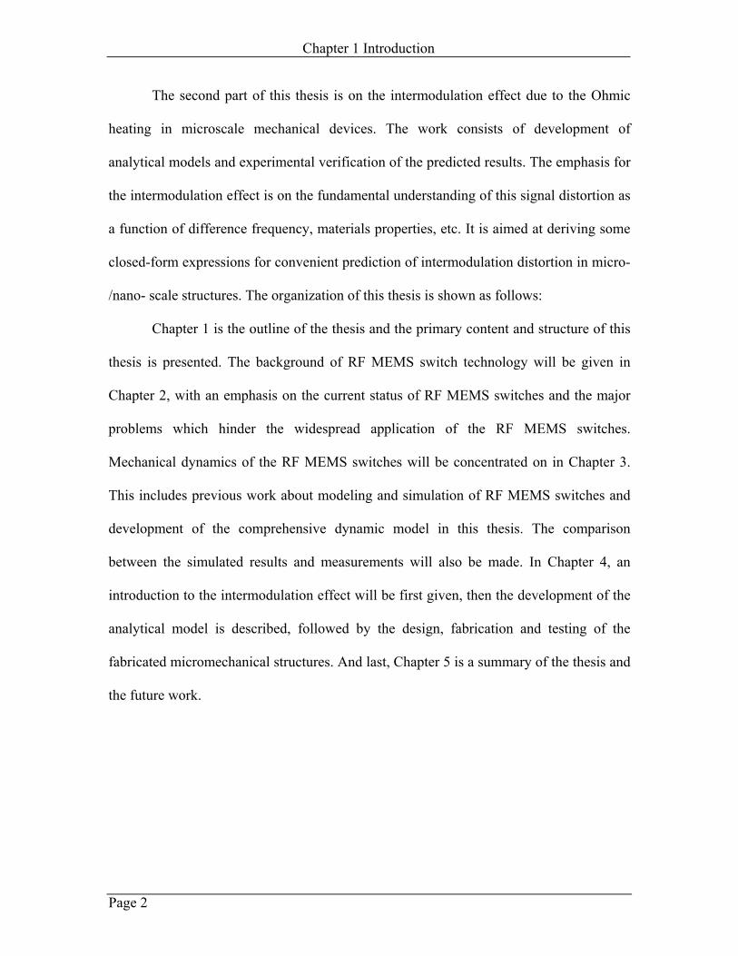
Much attention has been paid to RF MEMS switch technology since the first
micromechanical membrane-based switch was demonstrated by Petersen using
electrostatic actuation 55 . This is mainly due to the fact that conventional switching
devices such as GaAs-based metal-semiconductor field effect transistors (MESFETs) and
PIN diodes for high-speed switching can not meet the demanding requirements for RF
applications. For instance, silicon FETs can handle high power signal at low frequency,
but the performance drops off dramatically as frequency increases; others, such as GaAs
MESFETs work well at moderately high frequencies but only at low power levels. For
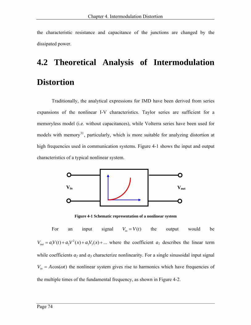
Chapter 2. Background of MEMS
Page 12
frequency greater than 1 GHz, these semiconductor switches have a large insertion loss
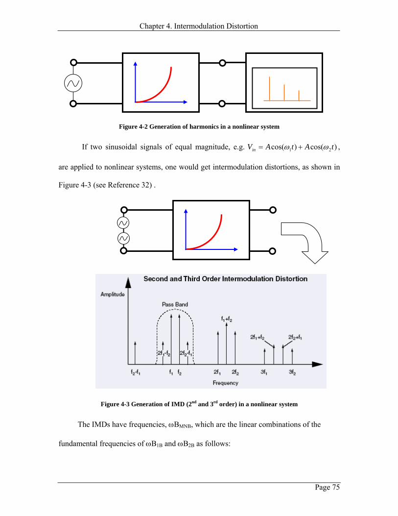
(typically 1- 2 dB) in the closed circuit state and a lower electrical isolation (typically 20
– 25 dB) in the open-circuit state. Also, the inherent junction capacitance of the
semiconductor based switches exhibits a larger nonlinear current versus voltage behavior,
leading to larger intermodulation distortion. However, the MEMS switches have a 3 P
rdP
order input intercept point (IP3) better than 65 dBm 54. This low loss, high isolation, and
high linearity are advantages of conventional electromagnetically-actuated mechanical
relays. On the other hand, like semiconductor switches, the MEMS switches have
smaller size, less weight, and fast switching in contrast to the electromagnetically
actuated mechanical relays. Therefore, MEMS switches combine the merits of both
semiconductor switches and mechanical relays.
2.2.3 Applications
As mentioned above, RF MEMS switches have low insertion loss, high isolation,
and high linearity for RF applications, compared with semiconductor-based solid-state
switches. At the same time, RF MEMS switches occupy little space, are not sensitive to
acceleration, have extremely low power consumption, have an extremely high cutoff
frequency of 20 – 80 THz, in contrast to 0.5 – 2 THz for MESFETs and 1.0 – 4.0 THz for
PIN diodes50 and are compatible with low cost silicon based IC technology. So, RF
MEMS switches have potential applications in a wide variety of areas. RF MEMS
switches can be used as a discrete switching component to switch signals. RF switches
can also be used as the building blocks of circuits such as phase shifters, which are
suitable for modern communications, automotive, and defense applications, low-loss
Chapter 2. Background of RF MEMS switch
Page 13
tunable circuits (matching networks, filter, etc) and high performance automatic
instrument testing systems, or subsystems or systems such as reconfigurable phased-array
antennas. Due to the cost of hermetic packaging of MEMS switches, the switches may
first be used in defense and high-value commercial applications. The following details
some example applications of RF MEMS switches:
Band switching and T/R Duplexers (TDD) in mobile phone or cellular phones56
Almost all the cellular or mobile phones on the market use a transmit/receive (T/R)
switch, or a band switch, and/or duplexers to interface the antenna and the chipset. The
use of any one or a combination of switching devices depends on the number of bands,
which is determined by the cellular phone system operator. Currently, compound
semiconductor such as GaAs and PIN diodes switches provide a reasonably good solution
to switching due to their power handling and flexibility. The overall performance of the
mobile phone or cellular phone could be greatly improved after RF MEMS switches
replace semiconductor-based counterparts in a multiband switching networks or T/R
switches in a T/R duplexer.
High frequency high Q digitized capacitor banks and phase-shifting networks
8:
The semiconductor switches, e.g. back-biased Schottky diodes, which are commonly
used in digital capacitor banks, have a low Q factor (Q ~ ωC/G in microwave and
millimeter wave applications). The RF MEMS switch may provide a high Q factor for
high frequency applications due to its inherent low loss characteristics.
Phase shifting is a popular control function at microwave and millimeter wave
frequencies. The reduction of occupation area and increase in accuracy in time-delay
phase shifting can be achieved using RF MEMS switches. One approach is to use a
Chapter 2. Background of MEMS
Page 14
coplanar-waveguide transmission line periodically with RF MEMS switches equally
distributed along the lineTPD
57DPT.
Applications in the defense area include phased array antennas, phased-array
radar, and satellite communications58 . Antennas used in military airborne crafts are
required to be able to handle high-data rates and possess large steering angles at
frequencies as high as Ku band (12.2 – 12.7 GHz). State-of-the-art phased array antennas
(PAA) are generally used for this application. The constructive interference of radiation
at PAA is realized through a high efficiency time-delay phase-shifting network, which
can be made possible through RF MEMS switches due to their intrinsically low insertion
loss and low-power consumption.
Other applications of RF MEMS switches are in automotive smart antenna, anti-
collision airbags, automotive GPS systems, base-stations for cellular phones, automatic
instrumentation, wireless LAN’s, data communications, digital personal assistants,
Bluetooth devices, etc.
2.2.4 Failure Mechanisms and Reliability Issues
As can be seen from the preceding discussions, the main driving force for much
effort on research and development of RF MEMS switches is their superior electrical
performance compared with existing semiconductor-based switches. As an emerging
technology, besides some inherent drawbacks with RF MEMS switches such as slow
switching speed, there are still concerns associated with RF MEMS switch technology.
To better understand the current status and potential problems, the following provides a
brief description of the issues related to the long-term reliability of microswitches, and
Chapter 2. Background of RF MEMS switch
Page 15
identifies some specific aspects which must be addressed before the RF MEMS switch is
widely accepted.
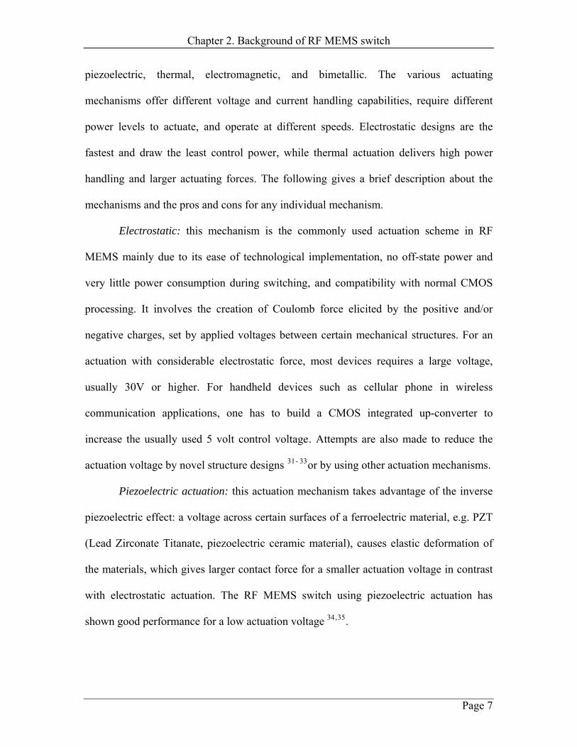
Compared with other actuation mechanisms, electrostatic actuation has the
advantages of being fast, easy to implement, and having virtually no power consumption.
However, electrostatic discharge (ESD) may cause failures to MEMS devicesTPD
59DPTP
- DDTD
61DTP. The
sudden build-up of a static charge on the MEMS device may result in potentials of over
one thousand volts, causing parts of the actuator or contact melt and weld together, which
may lead to the failure of the switch. It is generally recommended that proper precautions
should be taken before transport or handing of RF MEMS switches.
In general, electrostatically actuated MEMS switches use a relatively high
actuation voltage, usually on the order of 20 - 120V. From an application perspective,
high actuation voltages are not desired. To reduce the actuation voltage, one may use the
following methods: 1) increase the actuation area, 2) decrease the gap between the
electrodes, although this may decrease the electrical isolation during opening, 3) design
switches which have lower spring constant.
Alternatively, one may also provide an intermediary step that enables an RF
MEMS switch to operate at much lower voltages. A dc-dc voltage converter and
controller may be integrated with a high-voltage RF MEMS device to create a low-
voltage solution.
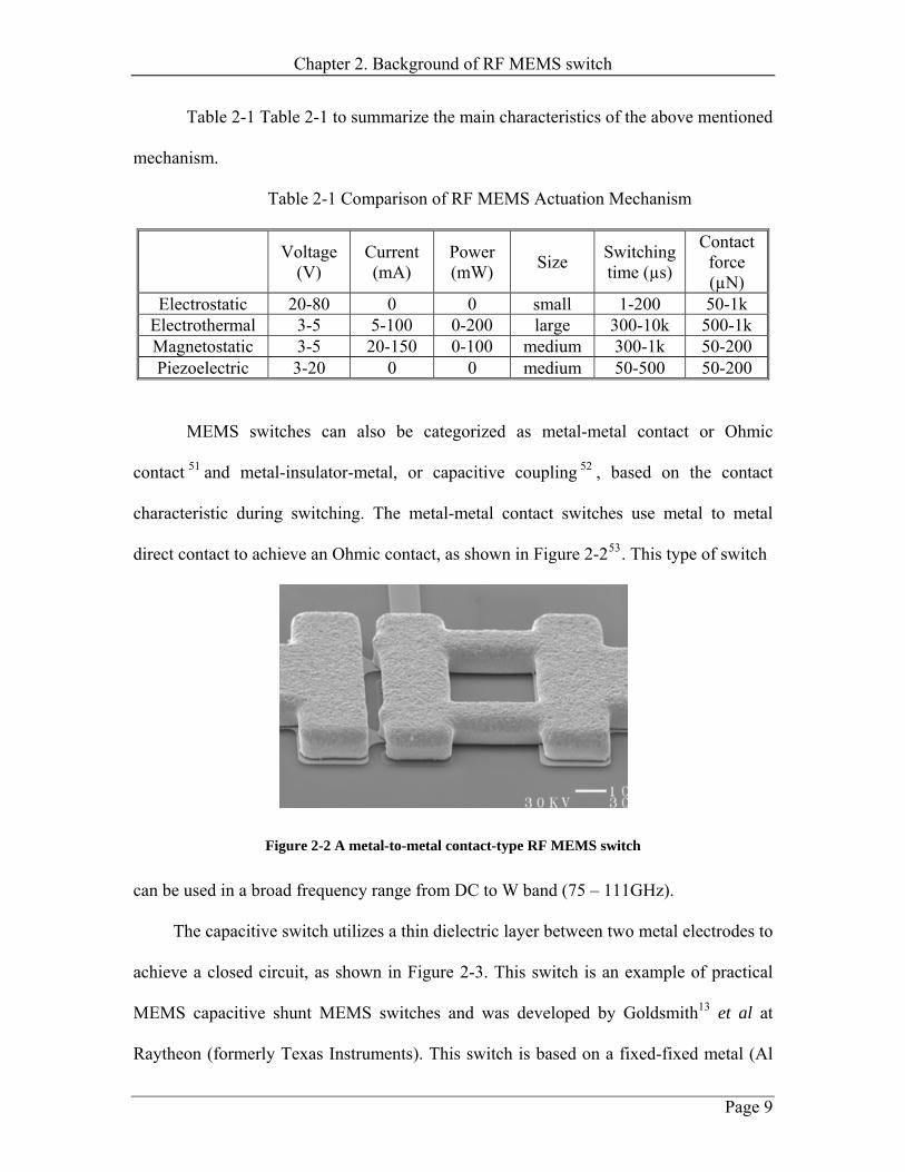
In addition to the above aspects which are relevant to RF MEMS switch
technology, another major concern about RF MEMS switches is its long-term reliability.
So far, the failure mechanisms are not completely understood, although it is observed that
the failure of a well-designed MEMS switch associated with mechanical malfunction
Chapter 2. Background of MEMS
Page 16
such as mechanical fatigue or even fracture is not usually a problem. It is also found that
most failures of current RF MEMS switches are associated with their contacts. The
reasons for mechanical failure at contact are very diverse and complicated. This is due to
the fact that contributing factors from different physical domains may have different
effects on failures. For instance, a simple Ohmic contact type switch may fail as a result
of a permanent stiction, or fail to open. The stiction may be caused by the increased
adhesive force during cycling, or due to degradation of contact with a larger contact area,
The second mode of failure associated with contact is the increase of resistance at the
contact after cycling. The switch is considered to fail if the contact resistance is larger
than a few ohms during operation.
It is believed that the reliability of the switch could be enhanced if one can
address the following issues properly:
(1) Contact materials: minimum adherence force at the contact interfaces is
desired for a better contact, near zero adherence force would be ideal;
(2) Actuation scheme: an optimized actuation scheme gives an optimum dynamic
behavior in terms of low impact force, reduced bounces;
(3) Thermal issues: low temperature of the switch is anticipated even when
handling high power;
(4) Resistance increase: it is often related to the chemically contaminated or
physically damaged contact.
In this thesis, we will deal with items (2) and (3). To study the dynamics of the
switch, we have used a finite element package ANSYS® and a finite difference method to
develop a comprehensive dynamic model. This model includes the complete structure of
Chapter 2. Background of RF MEMS switch
Page 17
the switch, squeeze-film damping, nonlinear contact, etch holes, and adherence force.
Afterwards, we use the model to optimize the dynamic performance of the switch. Also,
the simulated results are compared with the experiments. We also need to establish a
thermal model to investigate the thermally-induced intermodulation. Specifically, we first
build an analytical model to quantitatively examine the intermodulaton effect and design
the test device, and subsequently, make measurement on the fabricated device. Also, we
applied the developed method to predict the intermodulation distortion for a RF MEMS
switch. The intermodulation is caused primarily by Ohmic heating, since it is found that
the intermodulation caused by the change in contact resistance from the change in contact
force from the signal is much smaller than the thermally-induced intermodulation62.
Chapter 2. Background of MEMS
Page 18
References
TP
1H. C. Nathanson, W. E. Newell, R. A. Wickstrom, and J. R. Davis, Jr. “The Resonant Gate Transistor,”
IEEE Trans. Electron Devices, vol. 14, pp. 117-133, March 1967. 2 P. M. Zavracky and R. H. Morrison Jr., “Electrically actuated micromechanical switches with hysteresis,”
in Tech. Dig. IEEE Solid State Sensor Conf. Hilton Head Island, SC, June 6 - 8, 1984. 3K. E. Peterson, “Silicon torsional scanning mirror,” IBM J. Res. Develop., vol. 24, no. 5, pp. 631 – 637,
1980. 4ADXL105 datasheet, HTUhttp://www.analog.comUTH . 5P. Greiff, B. Boxenhorn, T. King, and L. Niles, “Silicon monolithic micromechanical gyroscope,” in Tech.
Dig. 6th Int. Conf. Solid-State Sensors and Actuators Transducers’ 91, San Francisco, CA, pp. 966 - 968,
June 1991. 6G. T. A. Kovacs, Micromachined Transducers Sourcebook, Boston, MA: McGraw-Hill, 1998. 7J. Brysek , K. Petersen, J. Mallon, L. Christel, F. Pourahmadi, Silicon Sensors and Microstructures, San
Jose, CA, 1990. 8E. R. Brown, “TRF-MEMS switches for reconfigurable integrated circuits,” IEEE Trans. Microwave and
Techniques, vol. 46, no.11, pp.868 - 880, 1998. T 9 J. Jason Yao, “RF MEMS from a device perspective,” J. Micromech. Microeng. vol.10, R.9 – 38, 2000T 10T. Zlatoljub D. Milosavljevic, “RF MEMS Switches”, Microwave Review, vol. 10, no.1, pp.1 - 9, June
2004. 11 T. Gabriel M. Rebeiz, “RF MEMS switches: status of the technology”, the 12PthP international
conference on solid-state sensors, actuators and microsystems, pp.1726 - 1729, Boston, June 8-12 2003.T 12T.S. Lucyszyn, “Review of radio frequency microelectromechanical systems technology”, IEE Proc. Sci.
Meas. Technol. vol. 151, no.2, pp.93 - 103, 2004.T 13 C. L. Goldsmith, Zhimin Yao, S. Eshelman, D. Denniston, “Performance of low-loss RF MEMS
capacitive switches”, IEEE Microwave and Guided Wave Letters, vol. 8, no. 8, pp.269 – 271, Aug. 1998. 14P. M. Zavracky, S. Majumder, N. E. McGruer T “Micromechanical switches fabricated using nickel
surface micromachining, ”J. Micromechanical Systems, vol. 6, pp. 3 - 9, 1997. 15 M. Innocent, P. Wambacq, S. Donnay, H. Tilmans, M. Engels, H. DeMan and W. SansenT “Analysis of
the Nonlinear Behavior of a MEMS Variable Capacitor,” Nanotech, vol.1, pp.234 – 237, 2002. 16 Imed Zine-El-Abidine, Michal Okoniewski and John G McRory, “Tunable radio frequency MEMS
inductors with thermal bimorph actuators,” J. Micromech. Microeng , vol.15, pp.2063 - 2068, 2005. 17Brian Bircumshawa,, Gang Liu, Hideki Takeuchi, Tsu-Jae King, Roger Howe, Oliver O’Reilly, Albert
Pisano “The radial bulk annular resonator: towards a 50 Ω RF MEMS filter”, The 12th International
Conference on Solid State Sensors, Actuators and Microsystems, pp.875 - 878, Boston, June 8 - 12, 2003.
Chapter 2. Background of RF MEMS switch
Page 19
18S. Pacheco, P. Zurcher, S. Young, D. Weston and W. Dauksher, “RF MEMS resonator for CMOS back-
end-of-line integration,” 2004 Topical Meeting on Silicon Monolithic Integrated Circuits in RF Systems,
Atlanta, GA, USA, pp. 203 - 206, Sept.8 - 10, 2004. 19 K. M. Strohm, F. J. Schmuckle, B. Schauwecker, J. F. Luy, “Silicon Micromachined RF MEMS
Resonators,” IEEE MTT-S Int. Microwave Symposium Digest, pp.1209-212, 2002. 20 S. V. Robertson, L. P. B. Katehi and G. M. Rebeiz,T “Micromachined W-band filters,” IEEE
Transactions on Microwave Theory and Techniques, vol. 44. no. 44, pp.598 – 606, 1996. 21James Brank, Jamie Yao, Mike Eberly, Andrew Malczewski, Karl Varian and Charles Goldsmith, “RF
MEMS-based tunable filters,”International Journal of RF and Microwave Computer-Aided Engineering,
vol.11, no.5 , pp. 276 – 284, 2001. 22D. Ramachandran, A. Oz, V. K. Saraf, G. Fedder and T. Mukherjee “MEMS-enabled Reconfigurable
VCO and RF Filter,” Proceedings of the 2004 IEEE Radio Frequency Integrated Circuits Symposium
(RFIC), pp. 251-254, Fort Worth, TX, June 6-8, 2004. 23 M. Behera, V. Kratyuk, Yutao Hu, and K. Mayaram, “Accurate simulation of phase noise in RF MEMS
VCOs” in Proceedings of the 2004 International Symposium on ISCAS ,V.3, pp.23 - 26 May 2004. 24A Malczewski, S. Eshelman, B. Pillans, and J. Ehmke, “X-band RF MEMS phase shifters for phased
array applications,” IEEE Microwave and Guided Wave Letters, 1999. 25Y Liu, A Borgioli, A. S Nagra, R. A York,” K-band 3-bit low-loss distributed MEMS phase shifter”,
IEEE Microwave and Guided Wave Letters, vol. 10, no. 10, pp.415 – 417, 1999. 26 B. Pillans, S. Eshelman, A. Malczewski, J. Ehmke, and C. Goldsmish, “Ka-band RF MEMS phase
shifters,” IEEE Microwave and Guided Wave Letters, vol. 9, no.12, pp. 520 – 522, December 1999. 27Atsushi Fukuda, Hiroshi Okazaki, Tetsuo Hirota and Yasushi Yamao, “Novel Band-Reconfigurable High
2005. 28K. Suzuki, S. Chen, T. Marumoto, Y. Ara, and R. Iwata, "A Micromachined RF Microswitch Applicable
to Phased-Array Antennas," IEEE MTT-S Symp Dig., Anaheim, pp.1923 - 1926, 1999. 29Kiriazi, J., H. Ghali, H. Ragaie, H. Haddara, “Reconfigurable Dual-Band Dipole Antenna on Silicon
Using Series MEMS Switches,” Antennas and Propagation, IEEE Society International Conference, 22–27
June, vol. 1, pp. 403 – 406, 2003. 30L. E. Larson, R. H. Hackett, M. A. Melendes, and R. F. Lohr, “Micromachined microwave actuator
(MIMAC) technology-a new tuning approach for microwave integrated circuits,” in Microwave and
millimeter-wave monolithic circuits symposium digest, Boston MA, pp. 27 - 30, June 1991. 31P. T. Sergio P. Pancheo, Linda P. B. Katehi and T. C. Nguyen, "Design of Low Actuation Voltage RF
MEMS Switch," Microwave Symposium Diges, IEEE MTT-S International, pp. 165 -168, 2000. 32 Shyh-Chiang Shen and Milton Feng, “Low Actuation Voltage RF MEMS Switches with Signal
Frequencies From 0.25 GHZ to 40 GHz," IEDM Technical Digest, pp. 689–692, 1999.
MEMS switch,” Microwave Symposium Digest, IEEE MTT-S International, vol.2 , pp.1225 -1228, 2002. 34Hee-Chul Lee, Jae-Hyoung Park, Jae-Yeong Park, Hyo-Jin Nam and Jong-Uk Bu, “Design, fabrication
and RF performances of two different types of piezoelectrically actuated Ohmic MEMS switches,”
Micromech. Microeng. vol.15, pp.2098 - 2104, 2005. 35G. Klaasse, B. Puers and H. A. C. Tilmans, “Piezoelectric actuation for application in RF-MEMS
switches,” SPIE-Int. Soc. Opt. Eng. Proceedings of Spie – the International Society for Optical
Engineering, vol.5455, no.1, Strasbourg, France, pp.174-80, Apr.29-30, 2004. 36Cho Il-Joo, Song Taeksang, Baek Sang-Hyun and Yoon Euisik, “A low-voltage push-pull SPDT RF
MEMS switch operated by combination of electromagnetic ctuation and electrostatic hold,” 18th IEEE
International Conference on Micro Electro Mechanical Systems, Miami Beach, FL, USA, pp.32-35, Jan.30-
Feb.3, 2005. 37 W. P. Taylor and M. G. Allen, “Integrated magnetic microrelays: normally open, normally closed, and
multi-pole devices,” Proceedings of International Solid-State Sensors and Actuators (Transducers ’97), pp.
1149–1152, 1997 38J. A. Wright, Y.-C. Tai, and G. Lilienthal, “A magnetostatic MEMS switch for DC brushless motor
commutation,” Proceedings of Solid-State Sensor and Actuator Workshop, pp. 304–307, 1998. 39 J. A. Wright and Y. C. Tai, “Micro-miniature electromagnetic switches fabricated using MEMS
technology,” Proceedings of 46th Annual International Relay Conference: NARM’98, pp. 131 –134, 1998. 40J. Wright, Y. C. Tai, and S.-C. Chang, “A large-force, fully integrated MEMS magnetic actuator,”
Proceedings of International Solid-State Sensors and Actuators (Transducers ’97), pp. 793–796, 1997. 41H. A. C. Tilmans, E. Fullin, H. Ziad, M. D. J. Van de Peer, J. Kesters, E. Van Geffen, J. Bergqvist, M.
Pantus, E. Beyne, K. Baert, and F. Naso, “A fully-packaged electromagnetic microrelay,” Proceedings of
IEEE International MEMS Conference, pp. 25 – 30, 1999. 42E. Fullin, J. Gobet, H. A. C. Tilmans, and J. Bergqvist, “A new basic technology for magnetic micro-
actuators,” Proceedings of IEEE International MEMS Conference, pp.143 – 147, 1998. 43J. W. Judy and R. S. Muller, “Batch-fabricated, addressable, magnetically actuated microstructures”,
Proceedings of Solid-State Sensor and Actuator Workshop, pp.187 – 190, 1996. 44L. K. Lagorce, O. Brand, and M. G. Allen, “Magnetic microactuators based on polymer magnets,”
Journal of Microelectromechanical Systems, vol. 8, pp. 2 – 9, 1999. 45M. Ruan, J. Shen and B. Wheeler, “Latching micromagnetic relays,” Journal of Microelectromechanical
Sysstems, vol. 10, no. 4, pp. 511 - 517, 2001. 46W. P. Taylor, O. Brand, and M. G. Allen, “Fully integrated magnetically actuated micromachined relays,”
Journal of Microelectromechanical Systems, vol. 7, pp.181 – 191, 1998.
Chapter 2. Background of RF MEMS switch
Page 21
47T. Blondy, P. Cros, D., Guillon, P., Rey, P., Charvet, P., Diem, B., Zanchi, C., Quoirin, J.B.” Low voltage
high isolation MEMS switches,” Topical Meeting on Silicon Monolithic Integrated Circuits in RF Systems,
pp. 47 – 49, 2001. 48P. T. Lai, B..K., Kahn, Harold, Phillips, S. M., Heuer, A. H., Quantitative Phase Transformation Behavior
in TiNi Shape Memory Alloy Thin Films, Journal of Materials Research, vol. 19, no. 10, pp.2822 - 2833,
2004. 49 H. Kahn, M. A. Huff, and A. H. Heuer, “The TiNi shape-memory alloy and its applications for MEMS,”
J. Micromech. Microeng vol.8,T pp. 213 - 221, 1998.T 50 G. M. Rebeiz, RF MEMS Theory, Design, and Technology, John Wiley & Sons, Inc., Hoboken, NJ, pp.4,
2003. 51P. M. Zavracky, N. E. McGruer, R.H. Morrison and D. Potter “Microswitches and Microrelays with a
View Toward Microwave Applications,” Int. J. RF Microwave: CAE’ vol. 9, no. 4, pp 338 – 347, 1999. 52S. Pacheco, C. T.-C. Nguyen, and L. P. B. Katehi, “Micromechanical electrostatic K-band switches,”
June 7-12, 1998. 53S. Majumder, J. Lampen, R.Morrison and J. Maciel “An Electrostatically Actuated Broadband MEMS
Switch,” Proceedings of Sensors Expo. Pp.23 - 26, Boston, Sept. 2002. 54Gabriel M. Rebeiz, Jeremy B. Muldavin, “RF MEMS switches and switch circuits,” IEEE microwave
magazine, pp.59 – 71, Dec. 2001. 55 K. E. Petersen, “Micromechanical membrane switches on silicon,” IBM Journal of Research and
Development, vol. 23, pp. 376 – 385, July 1979. 56 http://rfdesign.com/mag/radio_rf_mems_mobile/index.html 57N. S. Barker and G. M. Rebeiz, “Distributed MEMS True-Time Delay Phase Shifters and Wide-Band
Switches,” IEEE Trans. Microwave Theory Tech., vol.46, Apr. 1998. 58 G. M. Rebeiz, J. B. Muldavin, “RF MEMS switches and switch circuits,” IEEE Microwave Magazine,
pp.59 - 71, Dec. 2001. 59 S. A. Gasparyan and H. Shea, “Designing MEMS for reliability,” SPE Micromachining and
Mierafabrication Conference. Short Course M34, San Francisco, October 2001. 60T. Ono, Y. S. Dong, and M. Esashi, “Imaging of micro-discharge in a micro-gap of electrostatic actuator,”
in Proc. 13th Annu. Int. Conf.Micro Electro Mechanical Systems (MEMS 2000), pp.651 – 656, Jan. 2000. 61J. W. Minford and O. Sneh, “Apparatus and method for dissipating charge from lithium niobate devices,”
U.S. Patent 5, 949, 944, Oct. 2, 1997. 62 J. Johnson, G. G. Adams, N. E. McGruer, “Determination of intermodulation distortion in a contact-type MEMS microswitch,” IEEE Trans. Microwave Theory and Tech. vol. 53, pp. 3615 -3620, 2005.
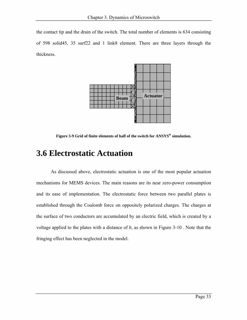
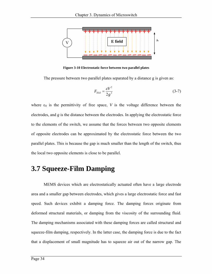
Chapter 3. Dynamics of Microswitch
Page 22
Chapter 3. Mechanical Dynamics of a
MEMS Switch
In this chapter, we will develop a comprehensive dynamic model using ANSYS®
(a software package based on the finite element method) in combination with a finite
difference method. First, we give a brief introduction to work on dynamics of MEMS
devices with an emphasis on RF MEMS switches. Then, we describe the modeling based
on finite element analysis, and after that we will describe models which are parts of the
comprehensive model for simulating dynamics of the switch This model includes solid
modeling of the switch using ANSYS®, electrostatic actuation, non-uniform squeeze-film
damping based on the Reynolds equation including compressibility and slip-flow, effects
of perforation of the beam on damping, nonlinear elastic contact and adherence force
during unloading. Finally, we present the experimental measurements and make
comparisons between the simulated results and the experimental measurements.
3.1 Dynamic Response of MEMS Switch
As mentioned in Chapter 1, MEMS switches promise to replace conventional
solid-state switches in many high frequency applications due to their enhanced
performance. For these applications, MEMS switches must be designed to be able to
operate for 1 to a few hundred billion cycles. The reliability of MEMS switches is
believed to be strongly connected to the dynamics of the actuation. It has been
Chapter 3. Dynamics of Microswitch
Page 23
experimentally observed that most failures occur at the contact, either because of stiction
due to large adherence force, or due to a substantial rise of the electrical resistance.
Impact force can flatten and increase the area of the contact leading to increased
adherence force. Contaminated contact and/or damaged contact resulting from fracture,
pitting, hardening, etc may cause switch resistance to increase. It is generally assumed
that if the contact resistance of the switch is 5 Ω or more, which corresponds to an
insertion loss of 0.5 dB in a 50 Ohm environment, the switch fails.
In general, the characterization of mechanical dynamics of the switch includes
actuation and release time, switching speed, impact force at contact, and bounce. All of
these properties are critical for the successful development of RF MEMS switches. But
among them, switching speed, impact force and bounce may be most critical, because
they are most relevant to the reliability of the switch.
During operation, the contact tip on the cantilever beam makes contact with the
drain, or signal transmission line. Before making steady contact, the contact tip usually
bounces several times due to the elastic energy stored in the deformed materials of the
actuator. The existence of bouncing behavior increases the effective closing time of the
switch. Meanwhile, the contact may be damaged by the impact force. This instantaneous
high impact force may induce local hardening or pitting of materials at the contact area.
The switch contact may also stick to the drain because of large adherence forces caused
by high impact force. Also, the bounces may facilitate material transfer, or contact wear-
out, which is not desired for a high-reliability switch. It has been experimentally observed
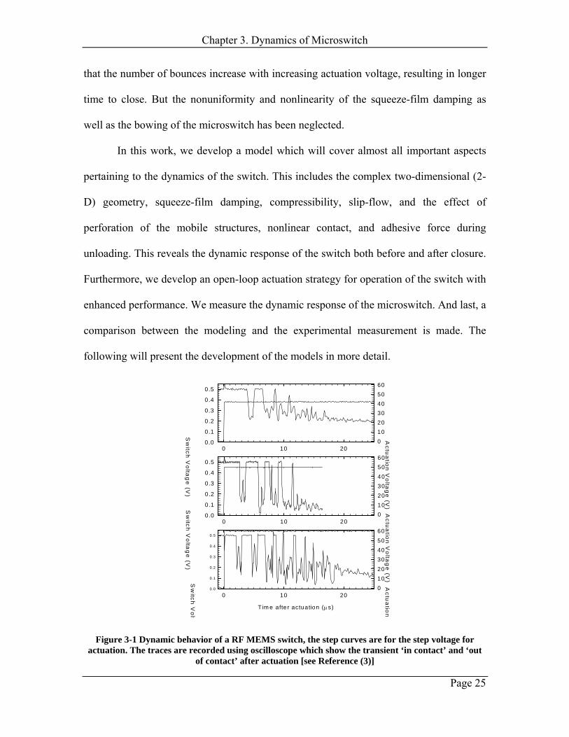
that the switches bounce a few times before making permanent contact1 -DPTDDDDDTD
5DTP. Elimination,
or at least reduction, of bounces is highly desirable for microswitches to operate with
Chapter 3. Dynamics of Microswitch
Page 24
longer lifetime and better performance. To control the dynamic behavior of the switch, it
is necessary to develop full dynamic models to simulate the dynamic response of the
microswitch.
Most dynamic models on MEMS switches account for only certain aspects of the
switch such as the squeeze-film damping, but contact characteristics and adhesions of the
microswitches during operation are not taken into account. For instance, Czaplewski et
al. 6 used a dynamic model to predict the dynamics of a Ohmic RF MEMS switch. But
the contact, squeeze-film damping, and adhesion effects have not been taken into account
in this model. The analytical analysis presented by Steeneken et al. 4 about the dynamics
of a capacitive RF MEMS switch mostly deals with the squeeze-film damping as well as
the slip-flow effects. Recently, Granaldi and Decuzzi 7 presented a one-dimensional
dynamic model which mainly focuses on the switching time and bouncing of a cantilever
based microswitch. In this model, the squeeze-film damping and the spring restoring
force have been lumped into two parameters, thus it does not take into account the
nonuniformity across the actuator and the nonlinearity of the damping force. Gee et al.8
presented a one-dimensional dynamic model and examined the effect of the dynamics of
the switch on its opening time. In that model, they used a fourth-order beam deflection
equation and included the adhesion force due to both van der Waals type forces and
metal-to-metal bonds. The one dimensional dynamic model developed by McCarthy et
al.3 based on a finite difference method for squeeze-film damping was used to simulate
the dynamics of the RF MEMS switch both before and after the contact. In that model,
the squeeze-film damping effect and a simple spring contact have been included, and the
spring shows the bouncing features after initial contact, as shown in Figure 3-1. It is seen
Chapter 3. Dynamics of Microswitch
Page 25
that the number of bounces increase with increasing actuation voltage, resulting in longer
time to close. But the nonuniformity and nonlinearity of the squeeze-film damping as
well as the bowing of the microswitch has been neglected.
In this work, we develop a model which will cover almost all important aspects
pertaining to the dynamics of the switch. This includes the complex two-dimensional (2-
D) geometry, squeeze-film damping, compressibility, slip-flow, and the effect of
perforation of the mobile structures, nonlinear contact, and adhesive force during
unloading. This reveals the dynamic response of the switch both before and after closure.
Furthermore, we develop an open-loop actuation strategy for operation of the switch with
enhanced performance. We measure the dynamic response of the microswitch. And last, a
comparison between the modeling and the experimental measurement is made. The
following will present the development of the models in more detail.
Figure 3-1 Dynamic behavior of a RF MEMS switch, the step curves are for the step voltage for actuation. The traces are recorded using oscilloscope which show the transient ‘in contact’ and ‘out
of contact’ after actuation [see Reference (3)]
T im e after actuation (µs)
0 10 20
Sw
itch V
olta
ge
(V)
0 .0
0.1
0.2
0.3
0.4
0.5
Actu
atio
n V
olta
ge
(V)
0102030405060
T im e after actuation (µs)
0 10 20
Sw
itch V
olta
ge
(V)
0 .0
0 .1
0.2
0.3
0.4
0.5
Actu
atio
n V
olta
ge
(V)
0102030405060
T im e after actuation (µs)
0 10 20
Sw
itch V
olt
0 .0
0.1
0.2
0.3
0.4
0.5
Actu
atio
n
0102030405060
Chapter 3. Dynamics of Microswitch
Page 26
3.2 Finite Element Analysis (FEA)
The finite element method is a numerical technique which has been used to solve
complex nonlinear problems in fields of research such as mechanical structures, fluid
mechanics, heat transfer, vibrations, electric and magnetic fields, acoustic engineering,
civil engineering, aeronautic engineering, and even in weather forecasting. The common
characteristic of FEA is the mesh descretization of a continuous domain into a set to
discrete sub-domains. In doing analysis of solid mechanics, a complex solid structure is
divided into a finite number of elements, and these elements are connected at points
called nodes. The stresses of each element are balanced by those of neighboring elements
and ultimately by the forces exerted on the exterior or at the boundaries. The
displacement of each node is determined by the overall displacement constrained by the
boundary conditions. Compared with analytical methods, FEA allows the simulation of a
generally complex geometry, and examination of the three-dimensional effects both
locally and globally.
In the modeling and simulation of dynamics of the RF MEMS switch, we used
ANSYSP
®P version 10.0, a FEA package from ANSYS Inc. The procedure of performing
simulation involves building solid model, material property designation, meshing, set-up
of boundary conditions, solving and post-processing. Before we go into the details of the
simulation, we need to introduce the aspects associated with the dynamics of the switch
such as lumped-parameter modeling, geometry and dimensions, electrostatic actuation,
squeeze-film damping, effect of etch holes, nonlinear contact, and adhesion.
Chapter 3. Dynamics of Microswitch
Page 27
3.3 Lumped Parameter Modeling of a
Cantilever Beam
Cantilever beams are often used as actuators in MEMS devices. The reasons
include the better understanding of the mechanical behavior and ease of fabrication. For
instance, cantilever beams are used in some inline series RF MEMS switches and
broadside switches, as discussed in Chapter 2. For applications of moving switches,
adjusting elements, valves and grippers, a DC voltage is applied, whereas for resonant
devices, an AC component is added to the driving voltage to excite the harmonic motions
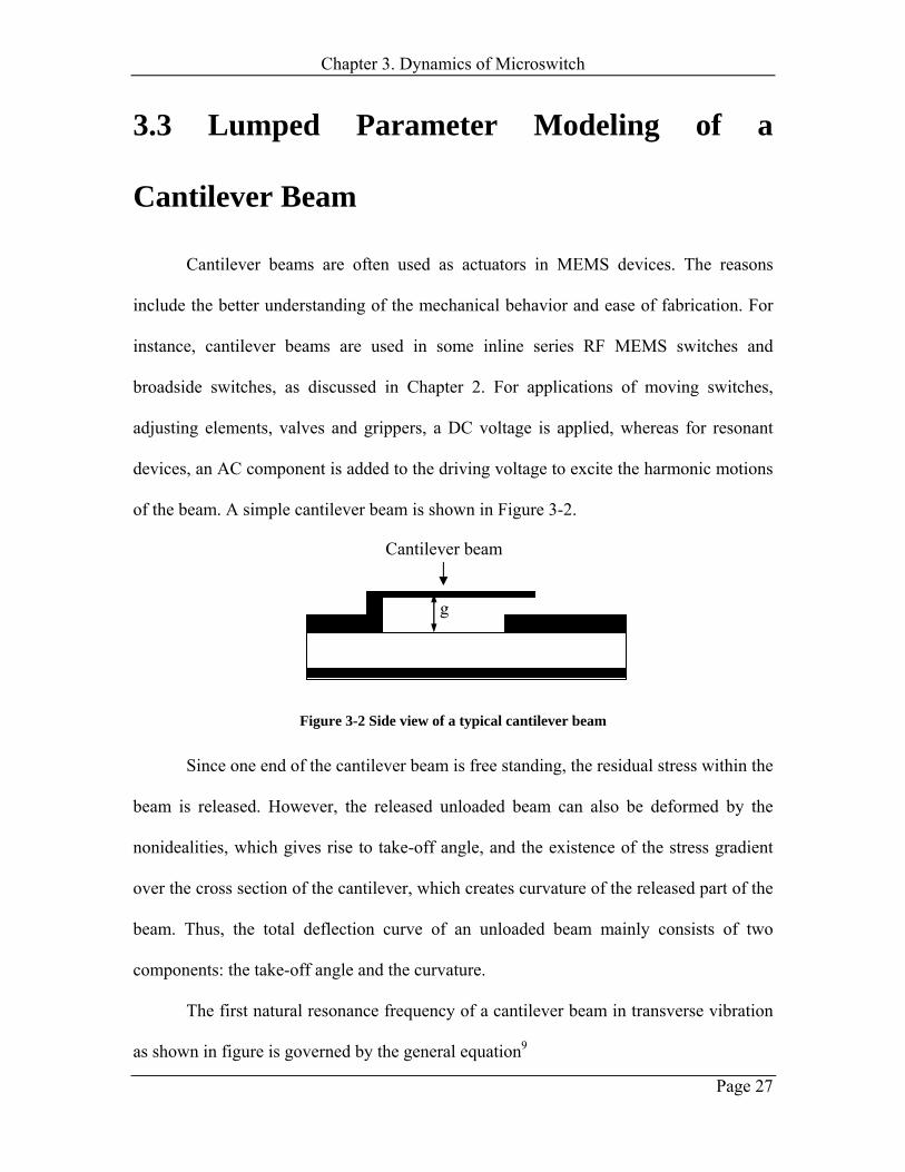
of the beam. A simple cantilever beam is shown in Figure 3-2.
Figure 3-2 Side view of a typical cantilever beam
Since one end of the cantilever beam is free standing, the residual stress within the
beam is released. However, the released unloaded beam can also be deformed by the
nonidealities, which gives rise to take-off angle, and the existence of the stress gradient
over the cross section of the cantilever, which creates curvature of the released part of the
beam. Thus, the total deflection curve of an unloaded beam mainly consists of two
components: the take-off angle and the curvature.
The first natural resonance frequency of a cantilever beam in transverse vibration
as shown in figure is governed by the general equation9
Cantilever beam
g
Chapter 3. Dynamics of Microswitch
Page 28
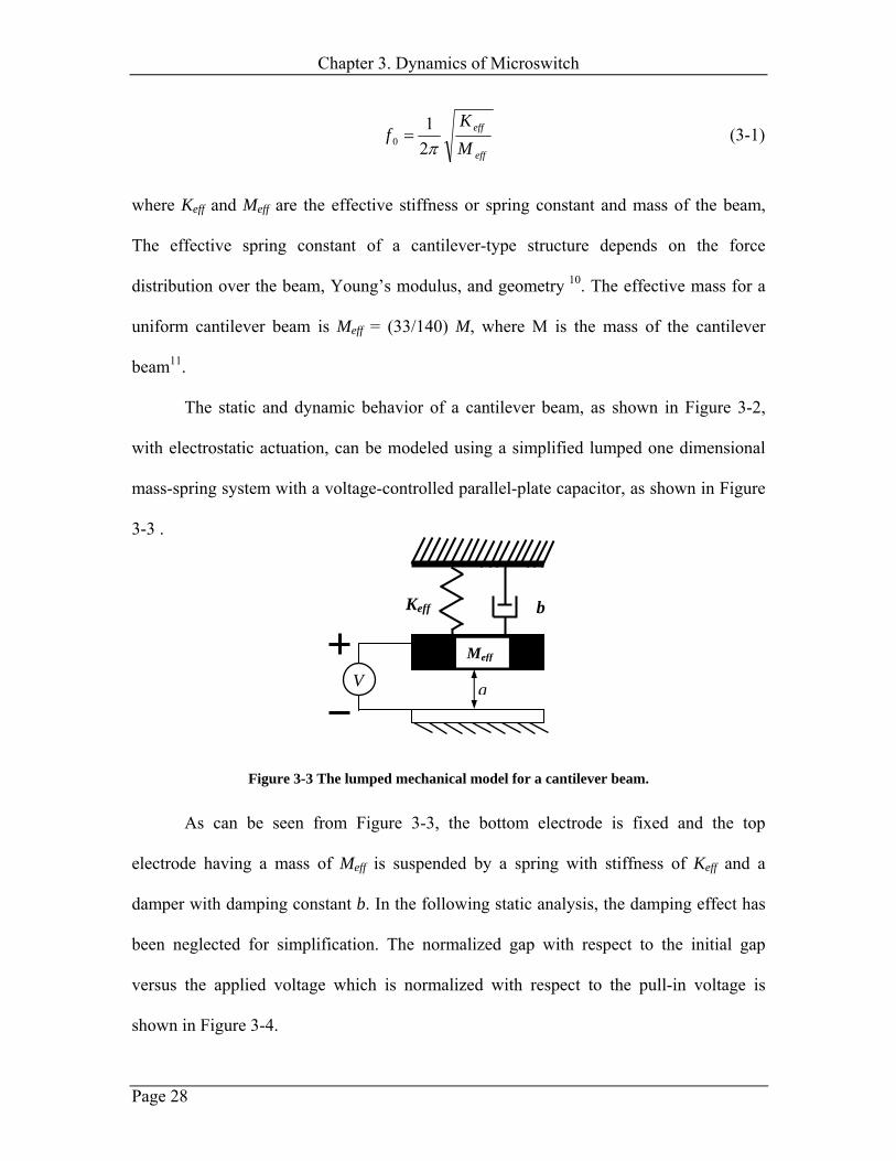
eff
eff
MK
fπ21
0 = (3-1)
where KBeffB and MBeffB are the effective stiffness or spring constant and mass of the beam,
The effective spring constant of a cantilever-type structure depends on the force
distribution over the beam, Young’s modulus, and geometry 10. The effective mass for a
uniform cantilever beam is MBeffB = (33/140) M, where M is the mass of the cantilever
beam11.
The static and dynamic behavior of a cantilever beam, as shown in Figure 3-2,
with electrostatic actuation, can be modeled using a simplified lumped one dimensional
mass-spring system with a voltage-controlled parallel-plate capacitor, as shown in Figure
3-3 .
Figure 3-3 The lumped mechanical model for a cantilever beam.
As can be seen from Figure 3-3, the bottom electrode is fixed and the top
electrode having a mass of MBeffB is suspended by a spring with stiffness of KBeffB and a
damper with damping constant b. In the following static analysis, the damping effect has
been neglected for simplification. The normalized gap with respect to the initial gap
versus the applied voltage which is normalized with respect to the pull-in voltage is
shown in Figure 3-4.
Keff b
VMeff
g
Chapter 3. Dynamics of Microswitch
Page 29
Figure 3-4 Gap of the cantilever vs. applied voltage
It can be seen that the system becomes unstable at g = (2/3)gB0 B due to the existence
of a forward feedback. At equilibrium when g > (2/3)gB0B, the electrostatic force pulling the
upper electrode down balances the spring restoring force which pulls the electrode upTPD
12DPT.
If the sign convention is assigned a positive sign for forces that increase the gap, the net
force on the upper electrode at voltage V and gap g is:
)(2 02
2
ggkgAVFnet −+
−=
ε (3-2)
where gB0 B is the gap at zero volts and zero spring extension. For this system to be stable at
the equilibrium point, the net force, FBnetB = 0, and the derivative of Eqn (3-2) has to be
less than or equal to zero. Then, at pull-in we have:
3
2
2 PI
PI
gAVk ε
= (3-3)
032 gg PI = (3-4)
A
kgVPI ε27
8 30= (3-5)
Stable
Unstable
Chapter 3. Dynamics of Microswitch
Page 30
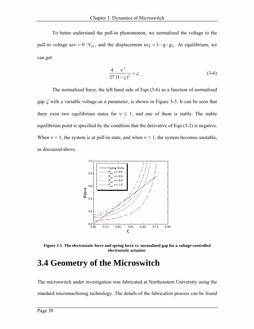
To better understand the pull-in phenomenon, we normalized the voltage to the
pull-in voltage as PIVV /=ν , and the displacement to 0/1 gg−=ς . At equilibrium, we
can get:
ςς
ν=
− 2
2
)1(274 (3-6)
The normalized force, the left hand side of Eqn (3-6) as a function of normalized
gap ζ with a variable voltage as a parameter, is shown in Figure 3-5. It can be seen that
there exist two equilibrium states for ν ≤ 1, and one of them is stable. The stable
equilibrium point is specified by the condition that the derivative of Eqn (3-2) is negative.
When ν = 1, the system is at pull-in state, and when ν > 1, the system becomes unstable,
as discussed above.
Figure 3-5 The electrostatic force and spring force vs. normalized gap for a voltage-controlled electrostatic actuator.
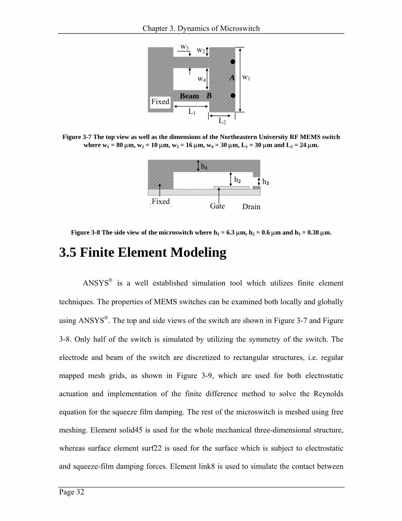
3.4 Geometry of the Microswitch
The microswitch under investigation was fabricated at Northeastern University using the
standard micromachining technology. The details of the fabrication process can be found
Chapter 3. Dynamics of Microswitch
Page 31
in the doctoral dissertation by Majumder 13. The switch is based on a cantilever-beam
type mechanical structure, as shown in Figure 3-6. The source, the actuator and the drain
of the microswitch is made of electroplated gold, and the gate is sputtered gold.
Figure 3-6 SEM micrograph of the Northeastern University MEMS switch.
The source end of the microswitch is attached to the substrate. The contacts
indicated on the figure make contact with the lower drain metallization (barely visible) in
the on-state.
The cantilever beam is actuated through the electrostatic force between the top
electrode, i.e. actuator, and the bottom electrodes, i.e. gate. The initial separation
between the top and bottom electrode is 0.6 µm before actuation. The top view along
with the dimensions of the microswitch is shown in Figure 3-7. The side view along with
the dimensions of the microswitch is shown in Figure 3-8.
ActuatorSource Drain
Gate
Contact
Chapter 3. Dynamics of Microswitch
Page 32
Figure 3-7 The top view as well as the dimensions of the Northeastern University RF MEMS switch
The switches under investigation have large, closely-spaced electrodes for
actuation. The gas between the electrodes, which are moving perpendicular to each other
during operation, is assumed to be compressible and isothermal. The mean free path of
air molecules at one atmosphere is about 62 nm, the initial gap between two electrodes is
Chapter 3. Dynamics of Microswitch
Page 37
600 nm. The Knudsen number is 0.1, so the slip-flow has to be taken into account in
calculating the damping force.
Without including the slip-flow effect, the Reynolds equation under isothermal
conditions for two parallel plates can be written as TPD
21DPTP
,TD
22
th
yph
yxph
x ∂∂
=∂∂
∂∂
+∂∂
∂∂ )(12)()( 33 ρµρρ (3-10)
where p is pressure, ρ is density, h is the distance between the electrodes, µ is the gas
viscosity is equal to 1.82 × 10⁻⁵ Pa⋅s for air at room temperature, and t is time. If the gas
is assumed to be ideal, the ideal gas law states that the gas density is proportional to the
pressure. The compressibility of the gas film is included by assuming the density is
proportional to the pressure for the idealized isothermal air gas. After including the slip-
flow effect, Eqn (3-10) can be modified to
tph
yph
yP
xph
xP
ypph
yxpph
x amam ∂∂
=∂∂
∂∂
+∂∂
∂∂
+∂∂
∂∂
+∂∂
∂∂ )(12)(6)(6)()( 2233 µλλ (3-11)
Eqn (3-11) shows that the pressure due to squeeze-film damping effect is a function of
position, height and time, that is, p = p(x, y, t). It is assumed that the pressure, also the
velocity of the gas molecule, is only dependent on x and y coordinates and not a function
of z.
As discussed above that the gas between the electrodes is modeled as a
compressible, continuous fluid, and undergoes an isothermal process during operation.
But, during operation of the MEMS switch, the damping force is not uniform since the
cantilever undergoes a movement which is location dependent. The equation has been
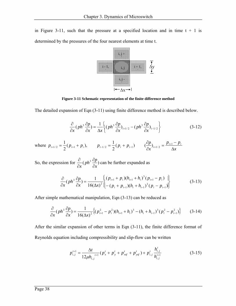
rewritten using the forward finite difference method, which was schematically illustrated
Chapter 3. Dynamics of Microswitch
Page 38
in Figure 3-11, such that the pressure at a specified location and in time t + 1 is
determined by the pressures of the four nearest elements at time t.
Figure 3-11 Schematic representation of the finite difference method
The detailed expansion of Eqn (3-11) using finite difference method is described below.
⎭⎬⎫
⎩⎨⎧
∂∂
−∂∂
∆=
∂∂
∂∂
−+ 2/13
2/133 )()(1)( ii x
pphxpph
xxpph
x (3-12)
where x
ppxppppppp ii
iiiiiii ∆−
=∂∂
+=+= ++−−++
12/112/112/1 )()(
21),(
21
So, the expression for )( 3
xpph
x ∂∂
∂∂ can be further expanded as
⎪⎭
⎪⎬⎫
⎪⎩
⎪⎨⎧
−++−
−++
∆=
∂∂
∂∂
−−−
+++
)())((
)())(()(16
1)(1
311
13
112
3
iiiiii
iiiiii
pphhpp
pphhppxx
pphx
(3-13)
After simple mathematical manipulation, Eqn (3-13) can be reduced as
)()())(()(16
1)( 21
231
31
2212
3−−++ −+−+−
∆=
∂∂
∂∂
iiiiiiii pphhhhppxx
pphx
(3-14)
After the similar expansion of other terms in Eqn (3-11), the finite difference format of
Reynolds equation including compressibility and slip-flow can be written
1,
,,1
,
1, )(
12 +++ ++++
∆= t
ji
tjit
jitysf
txsf
ty
txt
ji
tji h
hppppp
htp
µ (3-15)
∆y
∆x
i, j - 1
i + 1, j
i, j + 1
i - 1, j
i, j
Chapter 3. Dynamics of Microswitch
Page 39
where [ ] [ ]
2
2,
2,1
3,,1
2,
2,1
3,,1
)(16)()()()()()(
xpphhpphh
pt
jit
jit
jit
jit
jit
jit
jit
jitx ∆
−++−+= −−++ (3-16)
[ ] [ ]
2
2,
21,
3,1,
2,
21,
3,1,
)(16)()()()()()(
ypphhpphh
pt
jit
jit
jit
jit
jit
jit
jit
jity ∆
−++−+= −−++ (3-17)
[ ] [ ]
2,,1
2,,1,,1
2,,1
)(4)()(
xpphhpphh
Ppt
jit
jit
jit
jit
jit
jit
jit
jima
txsf ∆
−++−+= −−++λ (3-18)
[ ] [ ]
2,1,
2,1,,1,
2,1,
)(4)()(
ypphhpphh
Ppt
jit
jit
jit
jit
jit
jit
jit
jima
tysf ∆
−++−+= −−++λ (3-19)
where ∆t, ∆x and ∆y are the time increment, and the elemental distances in the x and y
directions, respectively. The tjih , term represents the distance of the element (i, j) from
the top to the bottom electrode at time step ‘t’. This explicit solution given by Eqn (3-15)
gives accurate results as long as the time step, ∆t, is sufficiently small for given values of
the spatial finite difference grid, ∆x and ∆y. In the simulation, the required time step is on
the order of nanosecond for a converged solution. Based on the preceding formulation, a
sequential simulation program has been developed for the transient simulation of the
dynamic response of the microswitch.
3.8 Effect of Perforation
The existence of holes on the cantilever may increase the switching speed of the
MEMS switch by reducing the squeeze-film damping, and facilitate the release of the
structures during fabrication. Usually, electrostaticly driven actuators have a relatively
large surface area, which may create problems in releasing them by etching processes.
Chapter 3. Dynamics of Microswitch
Page 40
On MEMS devices, particularly in cases where actuators of large area are used,
there may be some distributed etch holes on the actuator. The etch holes are generally
used to reduce the squeeze film damping as well as to facilitate the fabrication process
during the release process. Although there are no etch holes on the actuator of the current
version of the Northeastern University MEMS switch, we developed formulations which
account for the etch hole effect on squeeze-film damping in the following analysis.
The effect of etch holes on the damping has been included in analyzing the
dynamics of the planar microplateTPD
23DPTP
- 26DTP microscannerTPD
27DPT, microaccerometerP
28
,TD
28DTP, and
micromirrorTPD
29DPTP
,TD
30DTP. It was found that the number of the etch holes is more important than
the size of the holes in reducing the damping force. However, all models used an
equivalent damping coefficient in the Reynolds equation to calculate effect of the etch
holes on damping. In our work, we model the gas flow through the etch holes as a steady
fluid flow with slip flow boundary conditions. The advantage of this analysis is that the
effect of etch holes can be calculated using a finite difference method, thus can be
incorporated in the analysis in the previous section.
To include the effect of the etch holes in the compressible Reynolds equation, the
following formulations were performed. According to Gross31, the pressure p(x,y) inside
the gap can be written in terms of the velocity components u, v and w of gas molecules as
2
2
2
2
)(
)(
zv
zv
zyp
zu
zu
zxp
∂∂
=∂∂
∂∂
=∂∂
∂∂
=∂∂
∂∂
=∂∂
µµ
µµ (3-20)
where u and v are the velocity components in the x and y directions, respectively. The
absolute pressure p varies only with x and y. Assume that the velocity of the gas at the
Chapter 3. Dynamics of Microswitch
Page 41
bottom electrode and the bottom edge of holes with a gap height h is zero, that is, the
boundary conditions are
00
00
0
0
==
==
==
==
hzz
hzz
vv
uu (3-21)
After integrating Eqn (3-20) twice with boundary conditions of Eqns (3-21) we have
)(
21
)(21
2
2
zhzypv
zhzxpu
−∂∂
=
−∂∂
=
µ
µ (3-22)
According to the continuity equation32T, we have
0)()()( =∂∂
+∂∂
+∂∂
+∂∂ w
zv
yu
xtρρρρ (3-23)
Integrating Eqn (3-23), we have:
∫∫ ∂∂
+∂
∂+
∂∂
−=∂
∂ hh
dzty
vxudz
zw
00
])()([)( ρρρρ (3-24)
The left hand side (LHS) of Eqn (3-24) can be written as:
)()(0
0
Vthwdz
zw h
h
αρρρ+
∂∂
==∂
∂∫ (3-25)
where α is the area fraction of etch holes, V is the mean velocity in etch holes, and ρ is
the mass density. For our model, the values for α are 0.0428 and 0.0828, respectively, for
the front and end parts of the cantilever beam.
According to Munson et al., the mean velocity of gas, V, in the steady flow of a
pipe is given as 33
Chapter 3. Dynamics of Microswitch
Page 42
lR
ppV a
µαβ
αβ
8
)(
2
=
−= (3-26)
where R is the radius of the etch holes. In our case we assume we have 3 µm × 3 µm
square holes, R is the equivalent radius of a circular hole with the same area as the square
holes. P is the absolute pressure and PBa B is the pressure of the ambient environment, µ is
the viscosity of the gas, l is the height of the etch holes.
Substituting Eqn (3-26) into Eqn (3-25), we have:
)()(
0a
h
ppthdz
zw
−+∂∂
=∂
∂∫ βρρρ (3-27)
Substituting Eqn (3-22) into the right hand side (RHS) of Eqn (3-24), and after
integration over z from 0 to h, we have
thdz
t
yph
ydz
yv
xph
xdz
xu
h
h
h
∂∂
=∂∂
∂∂
∂∂
−=∂
∂
∂∂
∂∂
−=∂
∂
∫
∫
∫
ρρ
ρµ
ρ
ρµ
ρ
0
3
0
3
0
)(12
1)(
)(12
1)(
(3-28)
Substituting Eqn (3-28) into (3-24), we have
)()(12)()( '33appp
tph
ypph
yxpph
x−+
∂∂
=∂∂
∂∂
+∂∂
∂∂ βµ (3-29)
h
dπαβ2
3 2' = (3-30)
where d is the length of the edge of the square holes.
Chapter 3. Dynamics of Microswitch
Page 43
From Eqns (3-29) & (3-30), it can be seen that the effect of etch holes on the
pressure has been quantitatively associated with its geometry and pressure. Accordingly,
the pressure in the finite difference form including the slip-flow terms can be written as:
)(12
')(12 ,,11
,
,,1
,
1, a
tji
tjitt
ji
tjit
jitysf
txsf
ty
txt
ji
tji ppp
ht
hh
ppppphtp −
∆−++++
∆= +++
+
µβ
µ (3-31)
where txp , t
yp , txsfp and t
ysfp take the same forms as those in Eqns (3-16) - (3-19).
3.9 Nonlinear Contact Model with Adhesion
When the switch is actuated, the contact tip on the cantilever makes contact with
the drain. It is observed that typically only a few asperities with radius of curvature of
about 0.1 - 0.2 µm make contact with the bottom drain 13. The contact between the switch
tip on the upper beam and the drain can be modeled as the interaction between an
equivalent rigid spherical bump and a compliant flat surface. The widely used contact
models with adhesion are the Johnson-Kendall-Roberts (JKR) 34 and Derjaguin-Müller-
Toporov (DMT)35 models. The former is most appropriate for a larger radius bump, large
adhesion energy, and more compliant contact materials. The latter is best applied to cases
where interaction occurs between small and more rigid bumps with low adhesion energy.
A more quantitative dimensionless parameter, µ, defined by Tabor36 is used to determine
the regions of validity of the two models. This parameter is given as
3/1
30
2*
2
⎟⎟⎠
⎞⎜⎜⎝
⎛=
zERwµ (3-32)
where R is the radius of curvature of the bump and is 1.37µm, which corresponds to a
contact radius of 0.34 µm at a contact force of 1 mN for elastic deformation, w is
Chapter 3. Dynamics of Microswitch
Page 44
adhesion energy, E* is the effective Young’s modulus which is defined as 1/E* = (1-
ν12)/E1 + (1-ν2
2)/E2, and z0 is the equilibrium spacing of the surfaces in the Lennard-Jones
potential (typically z0 ≈ 0.28 nm for metals37).
For the case µ > 3, corresponding to larger radius bumps, lower Young’s moduli
and higher adhesion energy, the JKR theory is more applicable. On the other hand, if µ <
0.2, the DMT is more appropriate. In the microswitch, the electroplated Au is used as the
contact material, the Young’s modulus E = 42.4 GPa38 , Poisson’s ratio ν = 0.44, surface
energy γ = 1.37 J/m2 39 and adhesion energy w = 2γ. Substituting these values into Eqn.
(7), we found µ = 5.7, which indicates that the Au - Au contact is in the JKR regime.
Notice that we take the Young’s modulus value for electroplated gold from reference
[21]. It is reported that the Young’s modulus of the electroplated gold ranges from 41.9
GPa to 52.3 GPa40. In Section 3.1, it will be seen that the use of E = 42.4 GPa for
electroplated gold is a reasonable approximation for the real value.
The adhesion force for a JKR contact is 1.5πwR. According to JKR theory, the
contact radius, a, of a rigid sphere on a compliant flat surface with adhesion as a function
of load is given as 41
[ ]23 )3(63 wRwRPwRPKRa πππ +++= (3-33)
where K is the contact modulus and is equal to 4E*/3, and R is the effective radius of
curvature of the contact tip between Au and Au contact [16]. The adhesion force based on
JKR model is about 17.8 µN. Subsequently, the penetration, or displacement, of the
sphere relative to the drain can be written as:
Kaw
Ra
382 πδ −= (3-34)
Chapter 3. Dynamics of Microswitch
Page 45
It is clear that the penetration depends nonlinearly on the external force. This nonlinear
behavior is more reasonable than a linear spring given the fact that the contact area tends
to increase as the contact force increases, leading to a nonlinear stiffness which increases
with increasing deformation. As discussed above, contact is a very complex phenomenon,
i.e. elastic, elasto-plastic or even fully plastic deformation may all be involved. But for
simplicity, we assume that all plastic deformations occur during the first contact and,
subsequent loading and unloading are assumed to be purely elastic. To implement this
nonlinear elastic contact behavior, we used the link element Link8 in ANSYS® to
simulate the contact using Eqns (3-33) - (3-34).
Figure 3-12 The displacement of the microswitch contact tip vs. the contact force.
3.10 Dual-Pulse Scheme for Actuation
As discussed above, the long-term reliability of the MEMS switch is a major
concern. The mechanical dynamics of the switch are related to the reliability and
performance of the switch, because the impact force and bounces of the switch during
contact may deteriorate the contact physically and/or chemically. Meanwhile, switch
Chapter 3. Dynamics of Microswitch
Page 46
failure may be caused by increased stiction which results from repeated scrubbing and
flattening during operation. One way to improve the reliability of the switch is to tailor
the actuation waveforms such that a minimum impact force can be reached and thus
reduce the chances of creating local pitting and contact hardeningPD
42DPT. In the actuation of
PIN diode, a dual-pulse actuation method is often used. The first large current pulse is
injected into the wide depletion region and the device is turned on very quickly.
Afterwards, a lesser quiescent current maintains the device in the on-state TPD
43DPT. For the
MEMS switch, a similar idea may be applied to gently close the switch. The idea behind
this method is that a large actuation pulse is first applied to the switch, after a short period
of time, denoted as tB1 B, the pulse is turned off such that the speed of the switch is ideally
zero when it barely touches the bottom electrode at time tB2 B. The dynamic behavior of the
microswitch has been modeled using a simple lumped spring-mass damper system under
a contact force. A schematic representation of such system together with the pulses is
Figure 3-13.
Figure 3-13 (a) Lumped spring-mass system, (b) a typical profile for a dual-pulse actuation method,
and (c) the desired gradual close for a dual-pulse actuation
Notice that in this model, we used a constant force for modeling convenience
instead of a voltage to actuate the switch for simplicity. If we neglect the dependence of
the electrostatic force on the gap, the force is proportional to the square of the actuation
d
k
0 t1 t2
m
0
F
tt2 t1
F0
Fh
(a) (b)
0
d
tt2 t1
(c)
Chapter 3. Dynamics of Microswitch
Page 47
voltage. A voltage profile desired to eliminate bounce for gate actuation is shown in
Figure 3-13. A constant force of FB0 B, is first applied until time tB1B, and it will be removed
between time tB1 B and tB2B, which corresponds to the closing time of the microswitch. At time
t B2B, a second constant contact force FBh B is used to hold the switch. The second force of
smaller amplitude can reduce the impact force while maintaining a reasonable large
contact force. Notice that the velocity of the switch at time t B2B is expected to be close to
zero.
They can be expressed as follows:
⎩⎨⎧
><
=
−−=
0100
)(
)]()([)( 10
xx
xH
ttHtHFtF (3-35)
The displacement x for a system without damping )(tFkxxm =+&& ,
mkn =ω under load F(t) can be written as 44
110 ],cos)(cos1[)( ttttt
kFtx nn >−−−= ωω (3-36)
0)(,)(22== == tttt dt
tdxdtx (3-37)
Take the boundary conditions into Eqn (3-37), we have the following relationships
⎥⎦
⎤⎢⎣
⎡−
−= −
1
112 cos1
sintan2 t
ttn
nn
ωω
πτ (3-38)
⎥⎦
⎤⎢⎣
⎡= −
0
12 2
cos2 F
dkt n
πτ (3-39)
Chapter 3. Dynamics of Microswitch
Page 48
where nω and nτ are the angular frequency and period of the first mode of vibration. We
define FBthB = kd/3 as the threshold force, at which the snap down occurs. Then, Eqn (3-39)
becomes
⎥⎦
⎤⎢⎣
⎡= −
0
12 5.1cos
2 FFt thn
πτ (3-40)
In general, a voltage is used to actuate the gate of the microswitch. For a mass-
spring system, the voltage and force is related as follows
2
20
2dAVF ε
= (3-41)
From Eqn (3-41), it is seen that F is a function of voltage squared. So, Eqn (3-40) can be
approximated as
⎥⎥⎦
⎤
⎢⎢⎣
⎡⎟⎟⎠
⎞⎜⎜⎝
⎛= −
2
0
12 5.1cos
2 VVt thn
πτ (3-42)
Notice that Eqn (3-42) was derived with an assumption that F is constant. To keep a
constant force, we need to vary voltage with distance d, as seen in Eqn (3-41). We have
neglected this nonlinear effect to derive Eqn (3-42).
Chapter 3. Dynamics of Microswitch
Page 49
Figure 3-14 The relationship between the contact force, where ta is the actuation time, ton is the turn-on time, and Fa is the applied force. Note that ta and ton are normalized to the period of the first natural frequency, and Fa is normalized to a force Fth which corresponds to threshold voltage.
Figure 3-14 shows the relationship between contact force and time based on Eqns (3-38)
and (3-40). As a first order of approximation, the voltage is assumed to be proportional to
the square root of the electrostatic force. Figure 3-15 is the relationship of actuation
voltage normalized with respect to the threshold voltage as a function of time, based on
Eqns (3-38) and (3-42)(3-40).
Figure 3-15 The actuation time, ta, and the turn-on time, ton, for a dual voltage pulse method as a function of actuation voltage Va. Note that ta and ton are normalized to the period of the first natural
frequency, and Va is normalized to the threshold voltage.
Chapter 3. Dynamics of Microswitch
Page 50
3.11 Results and Discussion
As can be seen from above, a dynamic model which includes aspects that are
believed to be most relevant to the dynamics of the MEMS switch has been developed. In
the following, we will present the simulation results of the MEMS switch. To compare
with the experimental measurements, we first introduce the measurement setup, then
present the experimental measurement of the microswitch, and lastly, a comparison will
be made between the simulated and measured results.
3.11.1 Simulation Results
The switch used in the simulation is fabricated using electroplated gold. The
dimensions of the switch and the gap between the tip and drain as well as the initial gap
between the two electrodes were obtained using Zygo NewView 6000, as shown in
Figure 3-7 and Figure 3-8.
The switch is simulated at atmospheric pressure and at room temperature. We first
simulated the modal behavior of the switch. It was found that the first resonant frequency
of vibration is about 349 kHz in the open position and 1.77 MHz in the closed state. The
measured resonant frequency of vibration is 346 kHz in the open position. Notice that the
Young’s modulus for electroplated gold which is used in simulation is from the literature,
as discussed in Section 3.8. The excellent agreement between the measured and simulated
resonant frequencies of vibration suggests that the Young’s modulus value we used for
electroplated gold in the simulation is a good approximation to the real value. The
corresponding time periods are 2.86 µs and 0.57 µs, respectively. The simulated
Chapter 3. Dynamics of Microswitch
Page 51
threshold voltage (Vth) is about 65 V, which is in agreement with the measured values of
about 63 - 66 V.
Figure 3-16 shows the simulated displacement of the contact tip of the switch with
actuation voltages of 70 V, 74 V and 81 V. The corresponding initial contact times are
1.62 µs, 1.34 µs, 1.24 µs respectively. It is seen that the switch closes faster with larger
actuation voltage. However, the switch bounces with this single-step actuation and the
Figure 3-16 Contact tip displacements of the switch at actuation voltages of (a) 70V, (b) 74V, and (c) 81V.
number and magnitude of bounces increase with increasing actuation voltage. For each
case the magnitude of the bounces decreases with time due to the squeeze-film damping
effect.
The speed of the microswitch is important since it is related to the momentum of
the microswitch during operation. The velocity of the microswitch contact tip is obtained
as the first derivative of the contact tip displacement relative to time when the actuation
voltage is 81 V and is shown in Figure 3-17. Note that a positive velocity corresponds to
motion away from the surface. From Figure 3-17, the average acceleration of the
microswitch contact tip before the initial contact is about 44000 g. Notice that the
Chapter 3. Dynamics of Microswitch
Page 52
horizontal lines indicate the switch remains closed while the vertical lines for the sudden
change of switch from close to open state. The velocity when the switch moves toward
the lower drain is negative, otherwise it is positive.
Figure 3-17 The simulated contact tip velocity as a function of time for an actuation voltage of 81V.
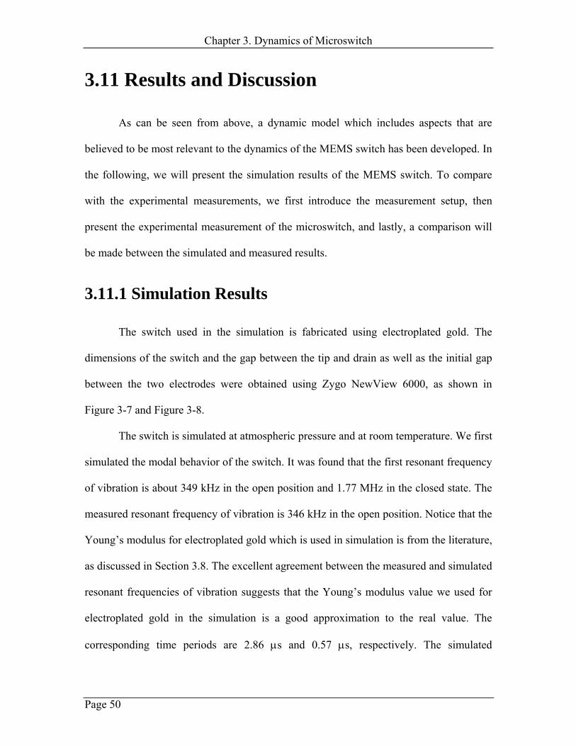
Figure 3-19 shows the displacements of the contact tip and of locations A and B,
as labeled in Figure 3-7 with an actuation voltage of 74 V. It can be clearly seen from the
motion of A in Figure 3-7 that the switch bends about 30 nm in the width direction while
the tips are in contact with the drain. The small difference of the motion between location
A and the tip is due to cross-bending of the actuator area due to the electrostatic force
exerted on it. In contrast, the displacement of location B is about half of that of location
A, due to the large stiffness of the switch in its closed position. For clarity, Figure 3-7 is
repeated here.
Chapter 3. Dynamics of Microswitch
Page 53
Figure 3-18 The top view as well as the dimensions of the Northeastern University RF MEMS switch
Figure 3-19 Comparison of displacements at different locations of the switch (see Figure 3-7) with an actuation voltage of 74 V.
The total squeeze-film damping force, the total electrostatic force on the actuator,
and the ratio of the absolute values of these forces are shown in Figure 3-20. It is seen
that both the electrostatic force and the squeeze-film damping force oscillate. This
behavior is caused by the bouncing dynamics of the switch after initial contact. We first
simulated the modal behavior of the switch. It was found that the first resonant frequency
of vibration is about 349 kHz in the open position and 1.77 MHz in the closed state. The
measured resonant frequency of vibration is 346 kHz in the open position. From Figure
3-20 (b), it can be seen that the damping force becomes negative when the switch start to
w3
w4
w2
A
L2
L1
w1
BBeam
Chapter 3. Dynamics of Microswitch
Page 54
bounce. Figure 3-20 (c) shows the ratio of the absolute values of the damping and
actuation forces. It is interesting to see that the damping force may significantly affect the
dynamics of the switch, since the damping force is dissipative and is as much as 13.5 %
of the electrostatic force for an actuation voltage of 1.1 times the threshold voltage. Also,
it can be seen that the damping force reaches its maximum just before the contact tip of
the switch makes initial contact with the drain. At this moment the gap attains its
minimum value and the speed is its maximum.
Figure 3-20 (a) Electrostatic force, Fe, (b) squeeze-film damping force, Fd, and (c) the ratio, ⎜Fd/Fe⎜, of their relative values with an actuation voltage of 74 V.
In order to see the evolution of the squeeze-film damping force, the distribution of
the squeeze-film pressure with respect to the atmosphere pressure, i.e. the gauge pressure,
across the gate area for an actuation voltage of 74 V is shown Figure 3-21. Before the
initial contact of the switch at times P1, P2, and P3 of Figure 3-21 (a), the maximum
pressure is located at the center of the gate, and it moves toward the contact tip edge. This
is because the local speed of the movable electrode near that edge is larger than that at
other locations and the corresponding separation is also smaller. After the contact tip
starts to bounce off the drain, the pressure at the edges first becomes negative and then
Chapter 3. Dynamics of Microswitch
Page 55
the negative pressure spreads to the middle of the gate when the contact tip reaches the
maximum bounce [see P4 and P5 in Figure 3-21 (a), (d) and (e)]. This means that the
squeeze-film damping force initially resists closing and then resists it from bouncing off.
Also, it is worth noting that the pressure at the center of the gate is positive even after the
switch bounces off the drain [see the gauge pressure distribution of point P4 in Figure
3-21 (d)]. This is due to the fact that air is compressible and the pressure due to
compression is greater than due to viscosity. From Figure 3-21 (c) it can be seen that the
0 1 2 3 4-0.4
-0.3
-0.2
-0.1
0.0
0 8 16 2480
70
60
50
40
3020
10
0
(e) @ P5(d) P4(c) @ P3
(b) @ P2(a) @ P1
02356891112
Gate Width (µm)
Gat
e Le
ngth
(µ
m)
0 8 16 2480
70
60
50
40
3020
10
0
03691215182124
Gate Width (µm)
0 8 16 240
10
20
3040
50
60
70
80
Gat
e Le
ngth
(µ
m)
-12-10-9-7-6-4-3-102
Gate Width (µm)0 8 16 24
80
70
60
5040
30
20
10
0
-10-8-7-6-5-4-2-101
Gate Width (µm)0 8 16 24
80
70
60
5040
30
20
10
0
0918263544536170
Gate Width (µm)
P5
P4
P3
P2
P1
Tip
Dis
plac
emen
t (µ
m)
T ime (µs)
Va=74 V
Figure 3-21 Evolution of the squeeze-film pressure distribution across the actuator at an actuation voltage of 74 V.
maximum gauge pressure occurs at the center of the gate and has a magnitude of about 60
kPa, i.e. approximately 60 % greater than atmospheric pressure.The slip-flow effect
becomes important when the minimum gap of the device is on the order of the
micrometer or less. To study the effect of slip-flow on the dynamic behavior of the
microswitch, the displacement of the microswitch tip for cases where the slip-flow terms
in Eqn.(3-15) are and are not included, are shown in Figure 3-22 for an actuation voltage
of 70 V. It is clearly seen from Figure 3-22 that both the switching speed and the duration
Chapter 3. Dynamics of Microswitch
Page 56
of bounces are reduced while the magnitude of bounce increases when the slip-flow
effect is included.
Figure 3-22 Comparison of the simulated microswitch contact tip displacement for cases with and without the slip-flow effect
After the contact tip of the switch makes contact with the drain, the instantaneous
contact force can be much larger than the static contact force. This is because the speed of
the switch is not zero when the contact between the contact tip and the drain occurs. In
the ANSYS® simulation, the instantaneous contact force along with the static contact
force at different actuation voltages are calculated and are shown in Figure 3-23. Here we
refer to the instantaneous contact force as the impact force. It is found that the maximum
impact forces are 5.6, 4.9, 4.5, and 4.2 times the static contact forces for actuation
voltages of 70V, 74V, 78V, and 81V, respectively. The ratio between the impact and
static forces decreases with increasing actuation voltage. This suggests that the higher
speed of the actuator causes a nonlinearly larger squeeze-film damping force for higher
actuation voltage, resulting in smaller ratio between the impact and static forces.
Chapter 3. Dynamics of Microswitch
Page 57
Figure 3-23 Impact forces, together with the static contact forces, of the switch with actuation voltages of (a) 70V, (b) 74 V, (c) 78 V, and (d) 81 V, respectively.
The control of the dynamics of the switch is important for its proper operation.
Some closed loop feedback control mechanisms are used to control the dynamics of a
moving mass45, but this procedure often needs additional circuitry to implement. An
alternative approach to control the dynamics of the switch is the open-loop tailored
actuation waveform method. A simple version of this mechanism is the dual voltage
pulse control method45. However, a thorough investigation is needed to understand and to
make this tailored waveform actuation more efficient for controlling the dynamics of the
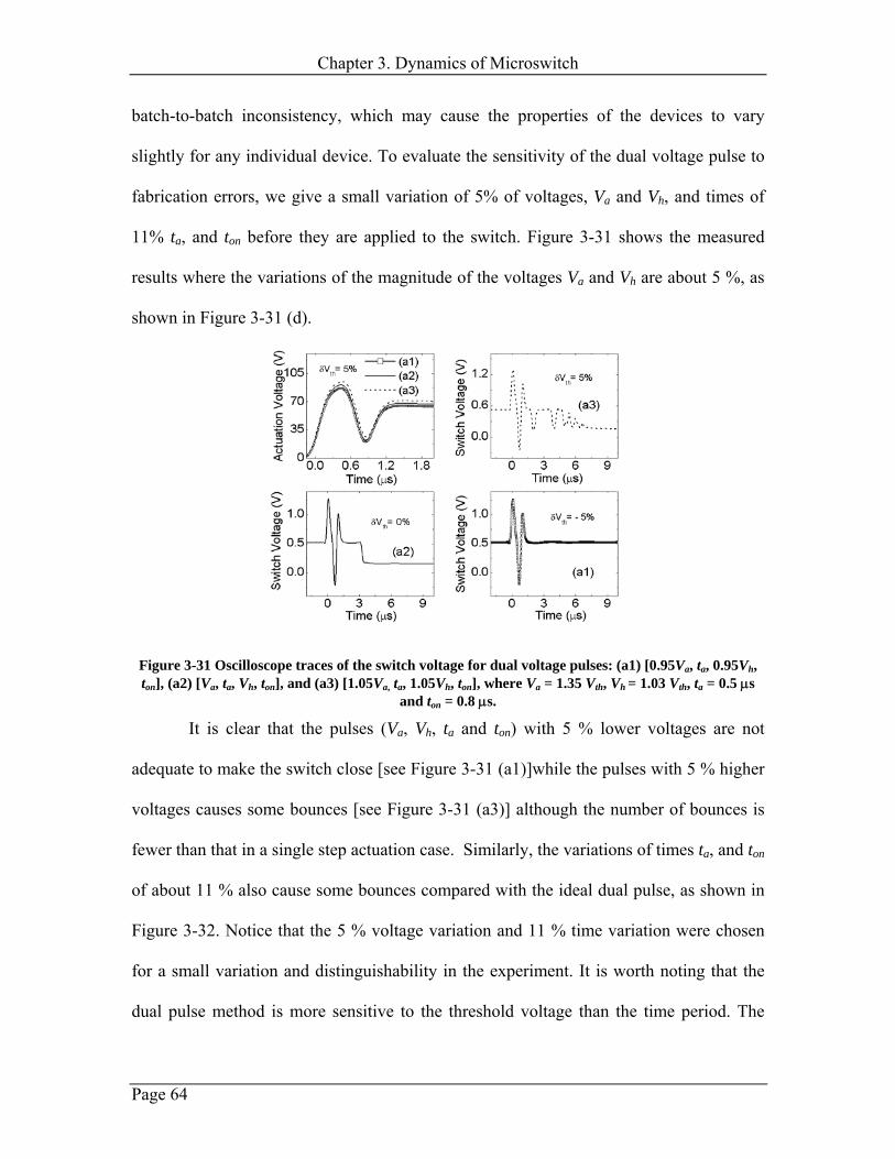
switch. By using the simplified results we have obtained in Section 3-10 as shown in
Figure 3-15, the simulation result using a dual-voltage pulse (Va = 88 V, ta = 0.8, Vh = 67
V, and ton = 1.05 µs) is shown in Figure 3-24. Compared with the single-step actuation,
this dual pulse can eliminate the bounce with a moderate impact force while maintaining
a fast switching speed. It is worth noting that the observed impact force oscillates with a
frequency of 1.2 MHz, which is smaller than the natural frequency of 1.77 MHz in the
closed state, after the contact tip is maintained in permanent contact with the drain. The
oscillating feature can be ascribed to the mechanical dynamics of the microswitch. The
Chapter 3. Dynamics of Microswitch
Page 58
maximum impact force for this dual-pulse actuation is about twice the static force for the
same holding voltage, and is about one third of the impact force (~ 96 µN) for the same
single-step actuation voltage of 67 V. This result indicates that the bounce for a dual-
pulse actuation can be completely eliminated whereas the impact force is still larger than
the static force for the same holding voltage.
Figure 3-24 Displacement of the contact tip using a dual pulse actuation, Va = 88 V, ta = 0.8, Vh = 67 V, and ton = 1.05 µs. The inset shows the impact force for this dual pulse actuation. The static force for a
single-step actuation voltage of 67 V gives a static force of 15 µN.
3.11.2 Comparisons Between Experiments and
Simulations
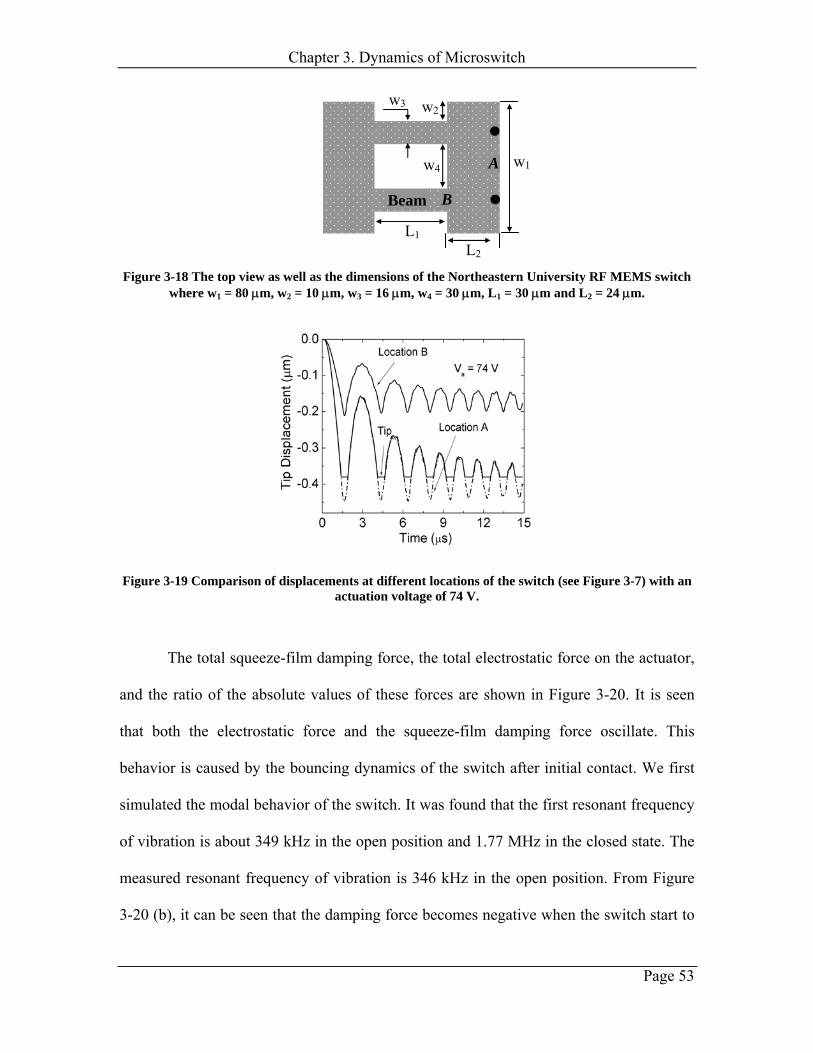
The experimental work has been performed on the switches which were
developed and fabricated at Northeastern University. The measurement circuit is shown
in Figure 3-25. An arbitrary waveform generator (Agilent 33220A Function /Arbitrary
waveform generator, 20 MHz) for programmed waveforms and a power amplifier (Apex
PA85A model) for large actuation voltages are used. The voltage across the switch is
recorded with an Agilent Infiniium 54830B oscilloscope: 2 Channels, 600 MHz,
Chapter 3. Dynamics of Microswitch
Page 59
sampling rate of up to 4 GSa/s. The total rise time, including the rise time of the function
generator and that of the amplifier for a single step voltage, is about 200 ns.
Figure 3-25 A schematic representation of the circuit and instruments used for experimental measurement.
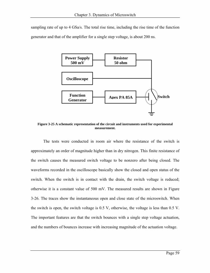
The tests were conducted in room air where the resistance of the switch is
approximately an order of magnitude higher than in dry nitrogen. This finite resistance of
the switch causes the measured switch voltage to be nonzero after being closed. The
waveforms recorded in the oscilloscope basically show the closed and open status of the
switch. When the switch is in contact with the drain, the switch voltage is reduced;
otherwise it is a constant value of 500 mV. The measured results are shown in Figure
3-26. The traces show the instantaneous open and close state of the microswitch. When
the switch is open, the switch voltage is 0.5 V, otherwise, the voltage is less than 0.5 V.
The important features are that the switch bounces with a single step voltage actuation,
and the numbers of bounces increase with increasing magnitude of the actuation voltage.
Power Supply 500 mV
Oscilloscope
Function Generator
Resistor 50 ohm
Apex PA 85A Switch
Chapter 3. Dynamics of Microswitch
Page 60
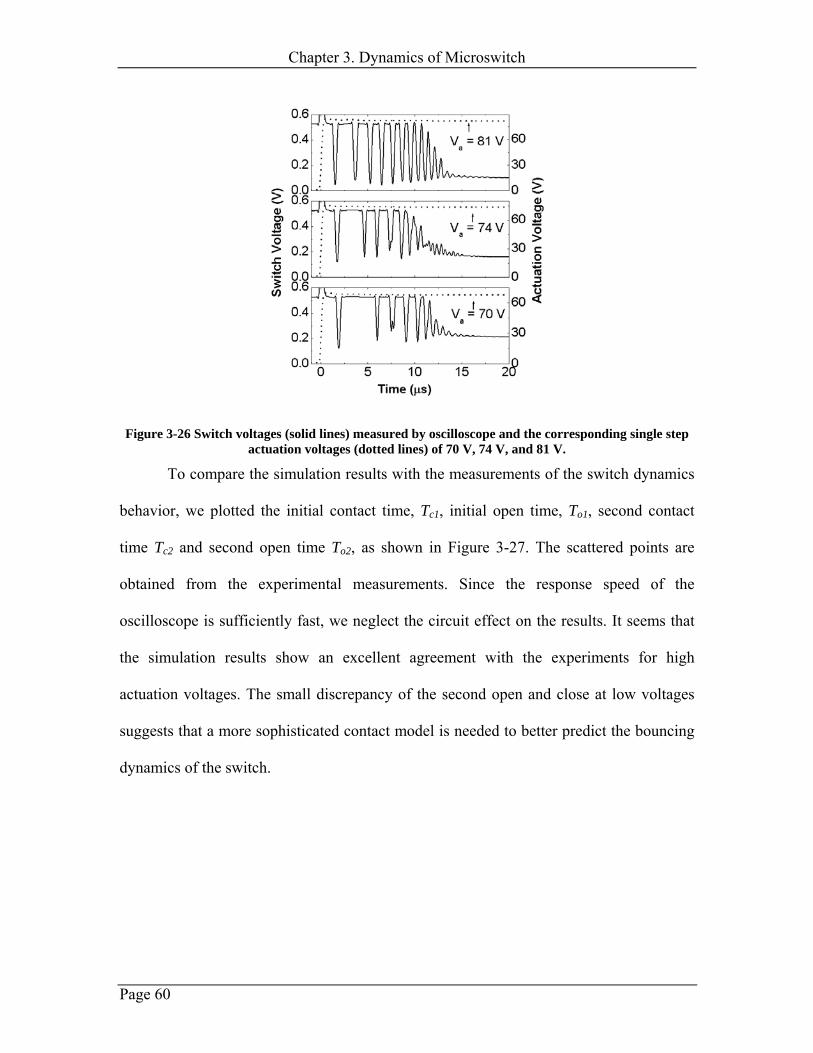
Figure 3-26 Switch voltages (solid lines) measured by oscilloscope and the corresponding single step actuation voltages (dotted lines) of 70 V, 74 V, and 81 V.
To compare the simulation results with the measurements of the switch dynamics
behavior, we plotted the initial contact time, Tc1, initial open time, To1, second contact
time Tc2 and second open time To2, as shown in Figure 3-27. The scattered points are
obtained from the experimental measurements. Since the response speed of the
oscilloscope is sufficiently fast, we neglect the circuit effect on the results. It seems that
the simulation results show an excellent agreement with the experiments for high
actuation voltages. The small discrepancy of the second open and close at low voltages
suggests that a more sophisticated contact model is needed to better predict the bouncing
dynamics of the switch.
Chapter 3. Dynamics of Microswitch
Page 61
Figure 3-27 Close and open times versus actuation voltage, where Tc1, To1, Tc2, To2 are 1st close time, 1st open time, 2nd close time, and 2nd open time, respectively. The scattered dots are experimental
results and the lines are from simulations.
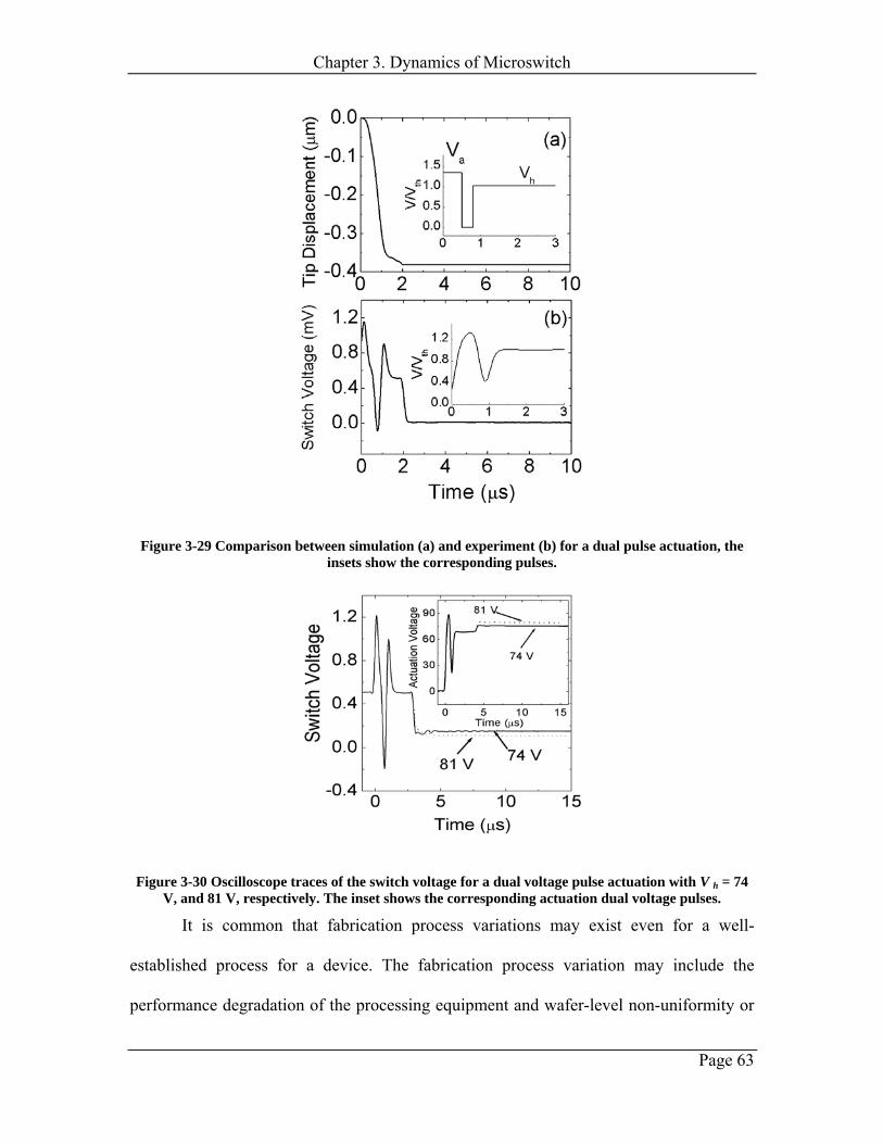
In the experiment for dual voltage pulse actuation, as shown in the inset of Figure
3-29(a), the values for Va, Vh, ta and ton are 1.5 Vth, 1.05 Vth, 0.5 µs, and 0.8 µs,
respectively, and are used in the function generator. Notice that since the first eigenperiod
of the switch is so short and the circuit has a finite rising and falling time, the expected
square shapes of the dual voltage pulses have been changed to triangle-like, as shown in
the inset of Figure 3-29(b). Notice that the observed peaks and valleys for time between 0
and 1.5 µs are caused by charging and discharging of the capacitor formed between the
actuator and the gate (Cag), which is coupled to the capacitor formed between the actuator
and the drain (Cad). Since these two capacitors have a common terminal, i.e. the actuator
of the switch, the charging or discharging of capacitor Cag will automatically charge or
discharge the capacitor Cad. In addition, the instantaneous current through the capacitor is
proportional to the rate of voltage change, i.e.dtdvCi = where C is the capacitance. To
include this effect, the waveforms are shaped to ensure that the work which is done on the
Chapter 3. Dynamics of Microswitch
Page 62
switch for both actuation waveforms is maintained about the same in the experiments. It
is clearly seen from Figure 3-29 that the simulated result is in an excellent agreement
with the experiment.
Figure 3-28 compares the timing of closing and opening events for both
simulations [Figure 3-16 (c)] and experiments (see Figure 3-26) at V = 81 V.
Figure 3-28 Comparison between the simulated and measured opening and closing times for an actuation voltage of 81 V. The horizontal axis is the number of closings or openings of the switch.
In the practical application of the switch, higher contact force is desired for
smaller contact resistance. In the dual voltage approach, one can intentionally increase
the voltage and thus the contact force once the switch gets closed permanently, as shown
in Figure 3-30. In this graph, the oscilloscope traces of the switch voltage are shown for
dual voltage pulses with varying holding voltage of 74 V and 81 V. The inset shows the
corresponding actuation pulses. It can be seen that for a higher holding voltage, e.g. 81 V,
the recorded switch voltage is lower than the one for lower holding voltage, e.g. 74 V,
due to a reduction of contact resistance induced by a higher contact force or holding
voltage.
Chapter 3. Dynamics of Microswitch
Page 63
Figure 3-29 Comparison between simulation (a) and experiment (b) for a dual pulse actuation, the insets show the corresponding pulses.
Figure 3-30 Oscilloscope traces of the switch voltage for a dual voltage pulse actuation with V h = 74 V, and 81 V, respectively. The inset shows the corresponding actuation dual voltage pulses.
It is common that fabrication process variations may exist even for a well-
established process for a device. The fabrication process variation may include the
performance degradation of the processing equipment and wafer-level non-uniformity or
Chapter 3. Dynamics of Microswitch
Page 64
batch-to-batch inconsistency, which may cause the properties of the devices to vary
slightly for any individual device. To evaluate the sensitivity of the dual voltage pulse to
fabrication errors, we give a small variation of 5% of voltages, Va and Vh, and times of
11% ta, and ton before they are applied to the switch. Figure 3-31 shows the measured
results where the variations of the magnitude of the voltages Va and Vh are about 5 %, as
shown in Figure 3-31 (d).
Figure 3-31 Oscilloscope traces of the switch voltage for dual voltage pulses: (a1) [0.95Va, ta, 0.95Vh, ton], (a2) [Va, ta, Vh, ton], and (a3) [1.05Va, ta, 1.05Vh, ton], where Va = 1.35 Vth, Vh = 1.03 Vth, ta = 0.5 µs
and ton = 0.8 µs.
It is clear that the pulses (Va, Vh, ta and ton) with 5 % lower voltages are not
adequate to make the switch close [see Figure 3-31 (a1)]while the pulses with 5 % higher
voltages causes some bounces [see Figure 3-31 (a3)] although the number of bounces is
fewer than that in a single step actuation case. Similarly, the variations of times ta, and ton
of about 11 % also cause some bounces compared with the ideal dual pulse, as shown in
Figure 3-32. Notice that the 5 % voltage variation and 11 % time variation were chosen
for a small variation and distinguishability in the experiment. It is worth noting that the
dual pulse method is more sensitive to the threshold voltage than the time period. The
Chapter 3. Dynamics of Microswitch
Page 65
observed results suggest that the dual pulse method may not be as efficient as expected in
terms of bounce elimination and impact force reduction if the switch parameters vary
significantly.
Figure 3-32 Oscilloscope traces of the switch voltage for dual voltage pulses: (b1) [(Va, 0.89ta, Vh, 0.89ton], (b2) [Va, ta, Vh, ton], and (b3) [(Va, 1.11 ta, Vh, 1.11ton], where Va = 1.35 Vth, Vh = 1.03 Vth, ta = 0.5
µs and ton = 0.8 µs.
As discussed above, squeeze-film damping plays an important role in determining
the dynamic response of the switch. One way to take advantage of the damping effect is
to design switches which have appropriate dimensions and geometries for critical
damping or moderate levels of damping during operation. Another alternative may to
intentionally increase the ambient pressure to some level for higher damping and better
operation, although this method may not be practical to implement for a switch. Figure
3-33 shows the simulation results of the dynamics of the switch which is actuated with a
single step voltage of 74 V but at pressures of 1 atmosphere and 10 atmospheres.
Chapter 3. Dynamics of Microswitch
Page 66
Figure 3-33 Simulated contact tip displacement of the switch at pressures of 1 atm and 10 atms for an actuation voltage of 74 V.
It is obvious that the magnitude and length of time of bounces are greatly reduced
when the switch is operated at a pressure of about 10 times atmospheric pressure
compared with operating at atmospheric pressure while the closing speed has not been
dramatically affected. This behavior is because at high ambient pressure, the squeeze-film
acts more as an incompressible squeeze-film than as a compressible one. It is noted that
the method of using high pressure to increase damping force on microswitch may not be a
practical solution in real applications. But the observed responses of the microswitch to
high ambient pressure suggest that one can intentionally increase the damping force to
improve the microswitch performance. For instance, one can increase the damping area
and/or decrease the gap between the actuator and the ground to achieve a larger squeeze-
film damping force in a MEMS switch design.
Chapter 3. Dynamics of Microswitch
Page 67
Reference
TP
1PT M. A. Gretillat, F. Gretillat and N. F. de Rooij, “Micromechanical relay with electrostatic actuation and
metallic contacts,” J. Micromech. Microeng. vol.9, pp. 324-331, 1999. 2D. Hyman, J. Lam, B. Warneke, A. Schmitz, T. Y. Hsu, J. Brown, J. Schaffner, A. Walston, R. Y. Loo, M.
Mehregany, J. Lee, “Surface-Micromachined RF MEMS switches on GaAs Substrates,” HTInternational
Journal of RF and Microwave Computer-Aided EngineeringTH, HTvolTH, Tpp. 348-361,T 1999. 3B. McCarthy, G. G. Adams, N. E. McGruer, and D. Potter, “A dynamic model, including contact bounces,
of an electrostatically actuated microswitch,” J. Micromechan. Sys., vol.11., pp.267-283, 2002. 4P. G. Steeneken, Th. G. S. M. Rijks, J. T. M. van Beek, M. J. E. Ulenaers, J. De Coster and R. Puers,
“Dynamics and squeeze-film gas damping of a capacitive RF MEMS switch,” J. Micromech. Microeng.
vol.15, pp.176–184, 2005. 5J. E. Massad, H. Sumali, D. S. Epp, and C. W. Dyck, “Modeling, simulation, and testing of the mechanical
dynamics of an rf mems switch,” Proceeding of the 2005 IEEE International conference on MEMS, NANO,
and Smart Systems, (ICMENS’05), pp.237-240, 2005. 6 D. A. Czaplewski, C. W. Dyck, H. Sumali, J. E. Massad, J. D. Kuppers, I. Reines, W. D. Cwan, and C. P.
Tigges, “A soft-landing waveforem for actuation of a single-pole single-throw ohmic RF MEMS switch,”
J. Microelectromechan Sys. 15, (2006), pp. 1586 – 1594. 7 A. Granaldi and P. Decuzzi, “The dynamic response of resistive microswitches: switching time and
bouncing,”J. Micromech. Microeng. vol.16, pp. 1108 - 1115, 2006. 8 G. Gee and B. D. Jensen, “A dynamic model of microscale contact breading in RF MEMS switches,”
Proc. of IJTC2006 STLE/ASME Int. Joint Tribology Conf., Oct. 22 - 25, 2006, San Antonio, TX, USA. 9 Inman D J 1996 Engineering Vibration 2nd edn (Englewood Cliffs, NJ: Prentice-Hall). 10G. M. Rebeiz, “RF MEMS Theory, Design, and Technology”. John Wiley & Sons, Inc., Hoboken, N. J,
pp.31, 2003. 11R. J. Wood, E. Steltz, and R.S. Fearing, “HTNonlinear performance limits for high energy density
piezoelectric bending actuators,TH” TIEEE Int. Conf on Robotics and AutomationT, Barcelona, Spain,
April 2005. 12S. D. Senturia, “Microsystem design” Kluwer Academic Publishers, Boston, 2001, P132 13 S. Majumder, Ph.D Dissertation, Northeastern University, Boston, 2003. 14W. E. Langlois, “Isothermal squeeze-films,” Quarterly Applied Mathematics, V. XX, No.2, 1962, pp 131-
150. 15W. A. Gross, “Gas film lubrication,” Wiley, New York, 1962. 16W. S. Griffin, H. H. Richardson and S. Yamamami, “A study of fluid squeeze-film damping”, J. Basic
Engineering, Trans. of ASME, June 1966, pp.451 – 456.
Chapter 3. Dynamics of Microswitch
Page 68
17J. J. Blech, “On isothermal squeeze-film”, J. Lubrication Technology, V.105, 1983, pp615 – 620. 18T. Veijola, A. Pursula, and P. Raback, “Surface extension model for MEMS squeezed-film dampers”,
Proceedings of DTIP 2005, Montreux, June 1-3, 2005, pp. 405-410. 19S. Dushman and J. M .Lafferty, “Scientific foundations of vacuum technique,” Wiley, New York, 1962. 20Y. Yang, squeeze-film damping for MEMS structures, Master’s thesis, MIT, USA, 1998 21J. Starr, “Squeeze-film damping in solid-state accelerometer,” IEEE workshop on solid-state sensor
actuator (Hilton Head Island, SC, USA, June 4-7), pp.44-47,1990. 22M. H. Sadd and A. K. Stiffler, “Squeeze-film dampers: amplitude effects at low squeeze number,” J. Eng.
Ind. B V.97 pp.1366-1370, 1975 23E. S. Kim, Y. H. Cho, and M. U. Kim, “Effect of holes and edges on the squeeze-film damping of
perforated micromechanical structures,” MEMS’99 (Orlando, FL, Jan.1999) pp 296–301. 24 D. Homentcovschi and R. N. Miles, “Modeling of viscous damping of perforated planarmicrostructures:
applications in acoustics,” J. Acoust. Soc. Am. 116 2939 – 2947, 2004. 25M. Bao, H. Yang, Y. Sun and P. J. French, “Modified Reynolds equation and analytical analysis of
squeeze-film air damping of perforated structures,” J. Micromech Microeng. 13, pp.795–800, 2003. 26T. Veijola and P. Raback, “A method for solving arbitrary MEMS perforation problems with rare gas
effects,” NSTI-Nanotech vol 3, pp 561– 564, 2005. 27 D. Yan andA. Lal, “The squeeze-film damping effect of perforated microscanners: modeling and
characterization,” Smart Mater. Struct. 15 (2006), pp.480–484. 28C. Bourgeois, F. Parret and A. Hoogerwer “Analytical model of squeeze-film damping in accelerometer”
Int. Conf. Solid State Sensors and Actuators (Chicago, IL, June 1997) pp 1117–20. 29K. M.Chang, S. C. Lee and S. H. Li, “Squeeze-film damping effect on a MEMS torsion mirror,” J.
Micromech. Microeng.12, pp.556–61, 2002. 30F. Pan, J. Kubby, E. Peeters, A. T. Tran and S. Mukherjee, “Squeeze-film damping effect on the dynamic
response of a MEMS torsion mirror,” J. Micromech. Microeng. 8 pp.200–208, 1998. 31W. A. Gross, L. A. Matsch, V. Castelli, A. Eshel, J. H. Vohr, M. Wildmann, “Fluid Film Lubrication”
P34, John Wiley & Sons Inc. 1980. 32B. Hamrock, “Fundamentals of Fluid Film Lubrication”. McGraw-Hill, Inc. New York, 1994. 33B. R. Munson, D. F. Young, T. H. Okiishi, “Fundamentals of fluid mechanics” P.369, 3PrdP Ed. John
Wiley & Sons Inc. 1998. 34K. L. Johnson and J. A. Greenwood, “An approximate JKR theory for elliptical contacts,” J. Phys. D:
Appl. Phys., vol. 38, pp. 1042 - 1046, 2005 35 B. V. Derjaguin, V. M. Mullerand, and Y. P. Toporov, “Effect of contact deformations on the adhesion of
particles,” J. Colloid Interface Sci., vol. 53, pp. 314 - 26, 1975. 36 D. Tabor, “Surface Forces and Surface Interactions,” J. Colloid Interface Sci., vol. 58, pp. 1 - 13, 1976.
Chapter 3. Dynamics of Microswitch
Page 69
37 D. Erts, A. Lohmus, R. Lohmus, H. Olin, A. V. Pokropivny, L. Ryen, and K. Svensson, “Force
interactions and adhesion of gold contacts using a combined atomic force microscope and transmission
electron microscope,” Appl. Surf. Sci., vol. 188, pp. 460 - 466, 2002. 38 J. Puigcorbe, S. Marco, S. Leseduarte, M. Carmona, O. Vendier, C. Devron, S. L. Delage, D. Floriot, and
H. Blanck, “Finite element modelling of flip chip gold-gold thermocompression bonding,” J. Elect.
Packag., vol. 125, pp. 549 - 555, 2003. 39 D. Maugis, Contact, Adhesion, and Rupture of Elastic Solids, Springer, Berlin, 2000. 40 C. W. Beak, Y. K. Kim, Y. M. Ahn, and Y. H. Kim, “Measurement of the mechanical properties of
electroplated gold thin films using micromachined beam structures,” Sensors and Actuators A, vol. 117, pp.
17 – 27, 2005. 41 K. L. Johnson, K. Kendall, and A. D. Roberts, “Surface energy and contact of elastic solids,” in Proc. of
the Royal Society of London, vol. 324, pp. 301 - 313, 1971 42 G. M. Rebeiz, RF MEMS theory, design, and technology, John Wiley & Sons, Inc. pp.192, 2003. 43 C. Goldsmith, J. Ehmke, A. Malczewski, B. Pillans, S. Eshelman, Z. Yao, J. Brank, and M. Eberly,
“Lifetime characterization of capacitive RF MEMS switches” in IEEE MTT-S Tech. Dig., Phoenix, AZ,
Jun. 2001, pp. 227–230 44 William T. Thomson, Marie Dillon Dahleh, Theory of vibration with applications, p. 98 5th ed. 1998,
Prentice-Hall, Inc. 45 B. Borovic, A. Q. Liu, D. Popa, H. Cai, and F. L. Lewis, “Open-loop versus closed-loop control of
MEMS devices: choices and issues,” J. Micromech. Microeng., vol. 15, pp. 1917 - 1924, 2005.
Chapter 4. Intermodulation Distortion
Page 70
H
Chapter 4. Intermodulation Distortion
In this chapter, we will investigate the intermodulation distortion (IMD) effect
associated with MEMS/NEMS devices. The intermodulation effect to be examined is
different from the conventional intermodulation effect in a nonlinear device. In a
traditional nonlinear device, the nonlinear transfer function between the input and output
signals gives rise to components which have frequencies that are sums and differences of
multiple integers of the two fundamental signals for a two-tone input signal. In the
contact-type microswitch, the nonlinearity of the Ohmic contact between two metals is
not important. But the thermal response of the device to the input signals creates variable
electrical resistance in the switch due to the temperature dependence of the electrical
resistivity of the switch materials. The modulation of the signals by the variable
resistance at a difference frequency for a two-tone signal results in the generation of
intermodulation distortion. This mechanism is termed thermally-induced intermodulation
distortion and has been observed previously in waveguides. In this chapter, we will
discuss the origin and the underlying mechanism of the thermally-induced
intermodulation in more detail. In a model system, consisting of a very small co-planar
waveguide, we will first develop a thermal model to predict the temperature. Second, we
present the expression for calculating the intermodulation in a circuit. The effect of the
materials properties on intermodulation distortion is examined in great detail. Third, the
simulation results are compared with the experimental measurements for the co-planar
Chapter 4. Intermodulation Distortion
Page 71
waveguide system. Finally, as an example, the derived expressions are applied to predict
the intermodulation expected for an Ohmic contact-type RF MEMS switch.
4.1 Intermodulation Effect
Intermodulation distortion refers to a physical phenomenon in which signals of
different frequencies transmit through an element or a system and produce new
frequencies that are sums and differences of the input frequencies.
If two tones of different frequency, f B1B and fB2B, are simultaneously applied as input
stimuli to a system, the overall output stimulus is a linear combination of the two
individual input stimuli. The amplitude of the two tones may be different. For a purely
linear system, the output response is simply the linear sum of the individual responses to
their associated pure input tones- no harmonics or other frequencies of any kind are
present. For a nonlinear system, the output waveform will have components which have
frequencies that are sums and differences of the input frequencies due to the nonlinear
mixing of the input signals.
Intermodulation distortion exists in devices, and circuits that contain nonlinear
devices. The devices include RF MOSFETsTPD
1DPT, GaAs MESFET’sTPD
2DPT microwave power
amplifiersTPD
3DPT, and PIN diodes due to the non-linear I-V characteristic at high frequencies
TPD
4DPTP
,TD
5DTP. For PIN diodes in high power applications, the effect of conductivity modulation by
the RF signal can be minimized by the stored charges, Qs = IBF Bτ, where IF is the forward
bias current, and τ is the minority carrier lifetime, in the wide I-regionTPD
6DPT. In comparison,
GaAs MESFETs are inherently lower power switching devices.
Chapter 4. Intermodulation Distortion
Page 72
As stated above, the intermodulation distortion in active semiconductor-based
components (amplifiers, etc) arises from nonlinear behavior due to the existence of p-n
junctions. The intermodulation distortion has also been observed in passive devices such
as microwave coaxial cavity filtersTPD
7DPT, duplexers, RF-cables, waveguides and antennas, and
is termed passive intermodulation distortion (PIM)TPD
8DPT It has been found that most of the
PIM’s occur due to the nonlinear contact and materials properties. The former refers to
any metallic contacts which have nonlinear current-voltage behavior, loose, oxidized and
contaminated metallic joints, electron tunneling, microdischarge, etc are typical examples.
PIM due to materials properties usually occurs in ferrites and ferromagnetic materials
such as nickel, cobalt etc.
Since the surfaces of any materials in contact have some degree of roughness at
the microscopic scale. Only a small portion of the nominal, or apparent, area of the
contacting surface is in real contact, and is termed as load bearing areaTPD
9DPT. Meanwhile, the
load bearing area can be further divided into metallic contact spots, quasi-metallic spots
separated by a thin film, and thick film coated area. For metallic contacts, the constriction
of current across the interface may dominate the flowing mechanism of the current,
whereas the electron tunneling effect predominate the behavior of the current flow across
the insulating thin film. The voltage breakdown phenomenon may occur for an interface
with thick insulating film. The PIM distortion has been observed in the metal-metal
contacts TPD
10DPT. The surface of most metals is covered by a thin layer of insulating materials.
The electrons may pass through the energy barrier created by the insulating film if they
can gain enough energy through thermal heating or electric fields. The electrons with
lower energy than the barrier can still have the probability of being able to overcome the
Chapter 4. Intermodulation Distortion
Page 73
energy hill. This phenomenon is called tunneling. The PIM phenomenon arising from the
tunneling effect has been experimentally investigatedTPD
11DPTP
,TD
12. The PIM effect due to the
nonlinearity of permeability in ferromagneticTPD
13DD
14DPT and ferrimagnetic materialsTPD
15DPTP
-DDTD
17DTPand
permittivity in dielectric materialsTPD
18 has also been reported.
MEMS devices designed for applications at RF, micro/millimeter wave
frequencies also exhibit intermodulation distortion effect. RF MEMS devices such as
SAW or FBAR filtersTPD
19DPT due to the nonlinear capacitance with gap displacement, silicon
beam resonatorTPD
20DPT due to nonlinear materials properties such as engineering Young’s
modulus, capacitive shunt switchesTPD
21DPT, variable capacitors TPD
22DPT,TPD
23DPT, micromechanical
resonatorsTPD
24DPT, cantilever-type MEMS switchesTPD
25DPT, etc. The intermodulation distortion in
most of the MEMS devices which contains a movable component is from an oscillatory
force with frequency less than the mechanical resonance frequency of the beam. In a
capacitive RF MEMS switch, the input signal causes the variation of the capacitance in
the up-state, which modulates the capacitance of the switch and results in the
intermodulation distortionTPD
26. For a GSM900 (global system mobile) outdoor base station,
the transmit power of a channel is typically 43 dBm and the receiver noise floor lower
than -110 dBmTPD
27DPT. It is not trivial for RF MEMS devices to fulfill this requirement. It has
recently been found that the self-heating appear to be important in generating
intermodulation distortion in microwave devices for high power multichannel
applicationsTPD
28DPTP
,TD
29DT
, TD
30DTP. The thermal effect in the active devices are calculated based on the
assumption that the drain current is reduced by thermal heating, and the decrease is
frequency dependent. Therefore, the basic idea about the thermal effect on the
intermodulation is the effect of the self-heating on the nonlinearitiy of the devices since
Chapter 4. Intermodulation Distortion
Page 74
the characteristic resistance and capacitance of the junctions are changed by the
dissipated power.
4.2 Theoretical Analysis of Intermodulation
Distortion
Traditionally, the analytical expressions for IMD have been derived from series
expansions of the nonlinear I-V characteristics. Taylor series are sufficient for a
memoryless model (i.e. without capacitances), while Volterra series have been used for
models with memoryTPD
31DPT, particularly, which is more suitable for analyzing distortion at
high frequencies used in communication systems. Figure 4-1 shows the input and output
characteristics of a typical nonlinear system.
Figure 4-1 Schematic representation of a nonlinear system
For an input signal )(tVVin = the output would be
...)()()( 332
21 +++= xVaxVatVaVout where the coefficient aB1 B describes the linear term
while coefficients aB2 B and aB3B characterize nonlinearity. For a single sinusoidal input signal
)cos( tAVin ω= the nonlinear system gives rise to harmonics which have frequencies of
the multiple times of the fundamental frequency, as shown in Figure 4-2.
Vin Vout
Chapter 4. Intermodulation Distortion
Page 75
Figure 4-2 Generation of harmonics in a nonlinear system
If two sinusoidal signals of equal magnitude, e.g. )cos()cos( 21 tAtAVin ωω += ,
are applied to nonlinear systems, one would get intermodulation distortions, as shown in
Figure 4-3 (see Reference 32) .
Figure 4-3 Generation of IMD (2nd and 3rd order) in a nonlinear system
The IMDs have frequencies, ωBMNB, which are the linear combinations of the
fundamental frequencies of ωB1B and ωB2B as follows:
Chapter 4. Intermodulation Distortion
Page 76
21 ωωω NMMN ±= (4-43)
where M, N = 1, 2, 3, …. Among the IMDs, the 3P
rdP 5th order IMD are technologically
more important than others for the performance of the system. For systems with broad
bandwidth, the intermodulation distortions of any order may affect the performance of the
systems. But, narrow bandwidth systems are only susceptible to the IMDs which fall
inside the passband. Bandpass filtering may be used to eliminate most of the unwanted
spurious signals. However, the 3P
rdP order intermoudlaiton products are usually too close to
the fundamental signals to be filtered out. As a practical example, in a cellular
communication system, if more than one signal from the transmitter is present in the
input to the receiver, IMD will be generated. Furthermore, if two signals are close enough
such as the 3 P
rdP order intermodulation product fall within the passband, it becomes
impossible to filter this distortion. In modern wireless communications systems, each cell
site often has multiple transmitters and receivers, The intermodulation distortion may
affect other receivers and/or transmitters operating near the transmitter frequency. In
particular, the third order intermodulation product may fall close enough to the carrier
signals and lies within the passband of the device in operation. In the cable between the
duplexer and the antenna in GSM base stations and in certain space applications where
the high power transmission and low power reception signals are carried simultaneously
in the same transmission line.
The third order intermodulation distortion denoted as IDB3 B is: 12
33 4/3 aAaID = .
The figure of merit for a nonlinear system is the third order input intercept point (IPB3B),
which is the input power in dBm for a point where the extrapolated output power is equal
Chapter 4. Intermodulation Distortion
Page 77
to that of the 3P
rdP order intermodulation distortion. The determination of IPB3B is shown in
Figure 4-4.
Figure 4-4 The 3rd order intermodulation power and output power versus input power
For RF MEMS switches the value of IPB3 B is 66 - 80 dBm, in contrast with 27 - 45
dBm for both FETs and PIN diodes 54.
4.3 Thermally-Induced PIM in MEMS Switch
As discussed in Chapter 2, the RF MEMS switches are believed to be very linear,
due to the absence of the nonlinear behavior of current vs. voltage curve. In a broadside
switch (see Figure 2-5), the signal path is decoupled from the actuation electrode.
Therefore, the intermodulation distortion due to the nonlinear variation of capacitance
arising from the motion of the electrode is also negligible. It is also known that the PIM
exists in a wide variety of passive devices although the exact underlying mechanisms are
not well understood. It is found that self-heating may be important under some
circumstances. As mentioned above, the intermodulation in active devices usually refers
to the nonlinear current vs. voltage curve. It is found that the thermal transients within the
active channel of the device in microwave active devices leads to deteriorated 3P
rdP order
Input power (dBm) IIP3
IMD3
Iout Pout(dBm)
Chapter 4. Intermodulation Distortion
Page 78
intermodulation distortion, particularly for smaller spacing between two tones TPD
33DPT.
WilcoxTPD
34DPT studied the PIM effect resulting from the thermal heating of a coaxial
waveguides walls. The instantaneous temperature variation is caused by the electrical
energy dissipation through thermal conduction with finite time constant. The interaction
of the conductance variation due to temperature variation with the electrical fields gives
rise to the third order intermodulation distortion. This effect is a pure PIM due to
thermally-induced variation of the electrical conductance in the coaxial waveguides.
Recently, the intermodulation distortion due to thermal effects was reported in an
RF MEMS switch 35DPT. The electrical resistance of the switch varies with the difference
frequency of a two-tone signal, resulting in a signal component with the difference
frequency. If the difference frequency between two input tones remixes either of the
fundamental frequencies, or two input tones are modulated by the resistance with a
frequency which is equal to the difference frequency, the 3P
rdP order intermodulation
frequencies may be produced. These 3P
rdP order intermodulation frequencies may also be
generated when the frequency fB1 B is mixed with the 2P
ndP harmonic of frequency fB2 B. But this
effect is smaller compared with the first mode since the second harmonic is much greater
than the inverse of the thermal time constant of the switch than the difference frequency.
It has been shown that the 3P
rdP order intermodualtion power for the switch can be written
as 35:
2
2'0
'03
)2(2 ⎥⎦
⎤⎢⎣
⎡+
=RR
RRPP
in
rd β (4-44)
For a particular switch, R is the load resistance of 50 Ω, R0’ is the resistance of
the switch, and β is the ratio of the switch resistance that has been increased by Ohmic
Chapter 4. Intermodulation Distortion
Page 79
heating to that at room temperature. By using Eqn (4-44), one can estimate the maximum
intermodulation distortion for RF MEMS switches or other MEMS devices. In addition, it
is reported that Ohmic heating exists in many MEMS devices. For instance, Chow et al.
36 reported the effect of self-heating on buckling, plasticity and power handling capability
in air-suspended RF MEMS transmission-line structures. They found the peak
temperature rise of 112 oC (average temperature of 73 oC) for a 0.5-W RF power input for
suspended CPW transmission lines. Mercado et al. 37 found that the temperature of the
RF MEMS switch contact could reach a few hundred degrees C for an input power of
0.36 W. As discussed above, due to Ohmic heating, an alternating signal may cause an
oscillating device temperature. The temperature-dependent electrical resistivity of the
device causes transient variation of electrical resistance with time-varying input signals,
yielding nonlinearity in the device. The modulation of the input signals by the variable
electrical resistance at the difference frequency for a two-tone signal may give rise to the
intermodulation distortion.
However, in the literature the quantitative analysis of this thermally-induced
intermodulation distortion in terms of materials properties and device geometry has not
been performed. To our best knowledge, the experimental study which is dedicated to
address the thermal-induced intermodulation distortion has not been conducted. In the
following, we will present both the theoretical and experimental investigation of the
thermally-induced intermodulation in a simple device. Then we extend the obtained
results to the RF MEMS switches.
Chapter 4. Intermodulation Distortion
Page 80
4.4 Design of a Model System
The need of high-power and broad-band transceivers in transmission line or
communication systems demands that the devices or systems of micro/nano meter scale
withstand being operated at an elevated temperature. Due to the intrinsic temperature
dependence of the thermal and electrical properties of materials, the electrical resistance
of the device varies with frequencies. The signals passing through the transmission line
may be modulated as a result of the variable electrical resistance of the device. For
example, for a two-tone signal the passive intermodulation may occur when the device
operates at high temperatures. In order to investigate the intermodulation effect arising
from the thermally modulated electrical resistance, we designed a simple system
consisting of a miniature coplanar waveguide which allows us to conveniently investigate
the thermally-induced intermodulation distortion.
4.4.1 Design Considerations
The refractory metal tungsten is used as the material of the model device because
it has a large temperature coefficient of resistivity and a high melting temperature, which
allows us to modulate the resistance of the devices, and thus the signal, in a wide range.
Contact pads are made of gold for ease of probing and for good contact between the gold
pads and the probe tips during the experiment. The device is made in a back-grounded
coplanar waveguide (CPW) configuration with a nominal characteristic impedance of 50
Ω. The CPW gaps for the devices are determined for a 50 Ω characteristic impedance for
a CPW transmission line using Txline, a shareware simulation program for transmissions
lines. The CPW grounds are tungsten, and the back-side ground is made of aluminum
Chapter 4. Intermodulation Distortion
Page 81
with a thickness of 1 µm. The tapered CPW transition angle of 30 degrees from a narrow
device to a wide pad is used for a smaller return loss 38. The geometry and dimensions of
the device are illustrated in Figure 4-5. The device was fabricated in Pyrex glass substrate
Figure 4-5 The geometry and dimensions of the device, not to scale (dimensions in µm).
using standard micromachining technology and optical lithography.
Since the device is expected to modulate the carrier signals through variable
electrical resistance, the dc electrical resistance of the device is designed to be fairly
large, in this case it is about ~ 40 Ω at room temperature.
4.4.2 Microfabrication
The device was fabricated using two masks and by means of standard
microfabrication techniques. The wafer level layout of the device in a three inch glass
wafer is shown in Figure 4-6. The die level layout of the device is shown in Figure 4-7.
Chapter 4. Intermodulation Distortion
Page 82
Figure 4-6 The wafer-level layout of the device
To further view the layout of the device, Figure 4-7 shows the layout of the device as
well as the PAD, and the layout of the device is shown in Figure 4-8. The pink color
represents tungsten structure and the light brown color is for gold pads.
Figure 4-7 The die-level layout of the device
Figure 4-8 The layout of the device
Chapter 4. Intermodulation Distortion
Page 83
The first mask is to define the device by dry etching tungsten using a mixture of
SF6 and Argon in an inductively coupled plasma (ICP) etcher. The gold pads are then
defined by the second mask and fabricated by means of a lift-off process. The substrate
we used in this study is Pyrex glass. Figure 4-9 shows the fabrication process, and the
process parameters can be found in Appendix A.
Figure 4-9 The process flow of the fabrication of the device
The physical properties of both tungsten and Pyrex glass are summarized in Table
4-1. Figure 4-10 shows the SEM micrograph together with the cross-sectional view of the
device.
Chapter 4. Intermodulation Distortion
Page 84
Table 4-1 Physical Properties of Device Materials Used in the Model
Density (kgm-3, ×103)
Thermal conductivity (Wm-1K-1)
Specific heat
(Jkg-1K-1)
Electrical resistivity
(Ωm, ×10-7)
Temp. coefficient of
resistivity (K-1, ×10-4)
Tungsten 19.3 173 133 3.1 9.0
Pyrex glass 2.23 1.4 835 > 10P
14P
N/A
Figure 4-10 (a) SEM micrograph of the fabricated device. (b) Cross-sectional view of a device, not to
In order to predict the intermodulation distortion generated by the variable
electrical resistance, we build a device as described above. Before we develop model to
predict the intermodulation, we need to establish a thermal model to determine the device
temperature in terms of materials properties, geometry and signal frequencies. We will
first develop the thermal model for the device we fabricated. The three-dimensional view
of the device is shown in Figure 4-11.
20µm
Substrate
Al
(a)
(b)
W2
H1
H2
H3
W1 W3G
Chapter 4. Intermodulation Distortion
Page 85
Figure 4-11 The three-dimensional view of the device on a pryex glass substrate
4.4.3.1 Thermal Modeling
As mentioned above, we need to develop a thermal model which can
quantitatively determine the temperature variation for an alternating input signal. In order
to build such a model system, we make the following assumptions: 1) we neglect the heat
transfer effect due to the CPW ground electrodes which can be seen in Figure 1; 2) we
assume the heat is generated only by the Ohmic heating of the device; 3) the temperature
across the whole device is uniform and the bottom aluminum electrode is maintained at
room temperature; and 4) we neglect the electrical skin effect at high frequencies and
assume a uniform current distribution over the cross section. This latter assumption is
verified by the calculation of the skin depth of tungsten at a frequency of 10 MHz, which
yields the skin depth of about 89 µm which is much larger than the width and the
thickness of the device. Figure 4-12 shows the schematic representation of the device for
thermal analysis.
Au
W
Substrate
Contact Pad
Chapter 4. Intermodulation Distortion
Page 86
Figure 4-12 The cross-sectional device-on-substrate schematic showing the heat generated by tungsten as uniformly distributed over a semicircle with a radius of half the width of the device, i.e. r1
= W2/2, and is transferred to the ambient through conduction. The arrows illustrate the isotropic nature of heat conduction, r2 = H2 + H3, not to scale.
The modes of heat transfer from the device to the ambient may be conduction
through the substrate, convection through the air, or radiation. To evaluate the relative
importance of the three different modes of heat transfer, we calculated the equivalent heat
transfer coefficient, h, of each mode. Since the dependencies of the heat transfer
coefficients of tungsten on temperature for different heat transfer modes vary
significantly, we need to choose a temperature or a range of temperatures at which we
calculate the heat transfer coefficient. In addition, thermal convection and thermal
radiation become more important than thermal conduction at high temperatures, so we
assume the device has a high temperature of about 2273 oK and the ambient temperature
is 300 oK. These assumptions give an upper-bound estimation of the importance of
radiation and convection relative to conduction.
According to the Stefan-Boltzmann law, the radiative heat transfer coefficient, hBr B,
can be written as 39
))(( 212
22
12,1 TTTTFhr ++= εσ (4-45)
Substrate
T = 300 K
r2
DeviceT
r1
Chapter 4. Intermodulation Distortion
Page 87
where ε is the emissivity of the radiating surface, σ is Stefan-Boltzmann constant (5.67 ×
10P
-8P WmP
-2PKP
-4P), FB1,2 B is the shape factor between surface area of body 1 and body 2, TB1 B and
TB2 B are the absolute temperatures of the device and ambient, respectively, ε = 0.23 for
tungsten at 2000 oC 40, and FB1,2 B = 0.5. Substituting the values of these constants in Eqn (4-
45) yields hBrB = 88.19 WmP
-2PKP
-1P.
For a free, or natural, heat convection in the air and the device facing up, the heat
transfer coefficient for a turbulent flow is given as 41
333.022.0 Thc ∆= (4-46)
where ∆T is the temperature difference between the device and the ambient air in degrees
Fahrenheit. A simple calculation shows that the heat transfer coefficient for free
convection is about hc = 2.75 WmP
-2PKP
-1.
For calculation of the heat transfer via thermal conduction through the substrate,
we need to take into account the spreading effect. The spreading angle for a thin and
infinite long plate is given as42
⎥⎥⎦
⎤
⎢⎢⎣
⎡⎟⎠⎞
⎜⎝⎛=
6.0
180355.0tanh90 K
sπθ (4-47)
where K is the thermal conductivity of the substrate. In our case, the spreading angles are
θS = 2.98P
o for a glass substrate. A simple calculation shows that the equivalent coefficient
of heat transfer for the conduction mode can be written as 42
))tan(1(wH
Khcondθ
+= (4-48)
For the geometry shown in Figure 4-12, hBcondB = 1.36 × 10P5 PWmP-2 PKP
-1 P
Chapter 4. Intermodulation Distortion
Page 88
From the preceding discussion, it can be seen that heat transfer by means of the
conduction mode is dominant, compared with those through natural convection and
thermal radiation. Thus, in the following derivation of the temperature variation of the
device, we neglect the heat loss due to convection and thermal radiation.
Since the dimensions of the tungsten device are much smaller than that of the
substrate and the length of the device is much larger than its width, the heat transfer
problem of the devices is analyzed in a cylindrical coordinate system to include the effect
of heat spreading in the lateral direction, as shown in Figure 4-12. When the signal
current flows through the tungsten device, the temperature of the device will increase due
to Ohmic heating. To simplify the analysis, we physically removed the device from the
substrate and assume that the heat generated by the device is uniformly distributed in a
half cylinder of radius of r1 which is equal to half the width of the device, and the
temperature of the device is equal to the center temperature of the cylinder. The heat
generated in the cylinder is transferred only through thermal conduction.
Heat energy generation due to Ohmic heating of two sinusoidal signals with equal
power delivery, i.e. [ ])sin()sin()( 210 ttItI ωω += , is
[ ] [ ]221011
21
221
20 )sin()sin(
2)sin()sin(2)( ttg
HrL
LrttItg e ωωρ
πωω
+=+
= (4-49)
where1
31
20
0 HrI
g e
πρ
= , ρBeB is the resistivity of the device, rB1 B and H1 are quantities as defined
in Figure 4-10, Figure 4-11 and Figure 4-12, the factor of 2 is used to double the power of
a full cylindrical configuration of the system.
The problem can then be formulated as a two-dimensional heat transfer boundary-
value problem together with boundary conditions, i.e.
Chapter 4. Intermodulation Distortion
Page 89
Let 0),(),( TtrTtr −=θ :
t
trrrHktg
rtr
rrtr
∂∂
=−+∂
∂+
∂∂ ),(1)()(),(1),(
12θ
αθθ (4-50)
00),(2
≥== ttr rrθ
00),( 20 ≥≥== rrtr tθ
where α = k/(ρBd BCBp B) is the thermal diffusivity of the substrate, r2 is taken to be equal to H2.
H(r1-r) is the unit step function as defined below
⎪⎩
⎪⎨
⎧
<−
≥−=−
)0(0
)0(1)(
1
1
1
rr
rrrrH (4-51)
Using the integral transfer method43, the kernel and eigenvalues for Eqn (4-50) in
the cylindrical coordinate system are
0)()()(2),( 20
21
0
2
=−= rJandrJrJ
rrK
m
mmm β
ββ
β (4-52)
where J B0B and J B1 B are the Bessel functions of the first kind of order 0 and order 1,
respectively, and β BmB are the eigenvalues of 0)( 20 =rJ β .
The solution to Eqn (4-50) can then be written as 43
∫∑ ∫∞
=
−= 222
0 01 02
21
02
2
)()'()()(2),(
r
nn
t
n
nt drtgrrJdterJrJ
ekr
tr nn βββαθ αβαβ (4-53)
As assumed above, the heat generation is only confined in a volume of a cylinder with a
radius of rB1 B, so Eqn (4-53) can then be reduced to
∫∑ ∫∞
=
−= 122
0 01 02
21
02
2
)'()()()(2),(
r
nn
t
n
nt drrrJdttgerJrJ
ekr
tr nn βββαθ αβαβ (4-54)
Chapter 4. Intermodulation Distortion
Page 90
Since )()( 10 rJrdrrrJ nn
n ββ
β =∫ 44, Eqn (4-54) can be further reduced to
∑ ∫∞
=
−=1 02
21
11012
2
)()(
)()(2),(22
n
t
nn
nnt dttgerJ
rJrJe
kr
rtr nn αβαβ
ββββα
θ (4-55)
Substituting Eqn (4-49) into Eqn (4-55) yields
[ ]∑ ∫∞
=
− +=1 0
221
221
11012
2
)sin()sin()(
)()(2),(22
n
t
nn
nnt dttterJ
rJrJe
kr
rtr nn ωω
ββββα
θ αβαβ (4-56)
To simplify Eqn (4-56) , let [ ]∫ +=t
n dttteF n
0
221 )sin()sin()(
2
ωωβ αβ , and 2nb αβ=
[ ]
[ ]
[ ]
[ ]⎭⎬⎫
⎩⎨⎧
++++++
−
⎭⎬⎫
⎩⎨⎧
−−+−+−
+
⎭⎬⎫
⎩⎨⎧
++
−
⎭⎬⎫
⎩⎨⎧
++
−
⎥⎦
⎤⎢⎣
⎡
+++
+−−
++
++−=
ttbb
e
ttbb
e
ttbb
e
ttbb
e
bbbbb
bbeF
bt
bt
bt
bt
bt
n
)sin()()cos()(
)sin()()cos()(
)2sin(2)2cos(42
1
)2sin(2)2cos(42
1
)(1
)(1
41
411)(
2121212221
2121212221
222222
111221
221
221
222
221
ωωωωωωωω
ωωωωωωωω
ωωωω
ωωωω
ωωωωωωβ
(4-57)
After making substitution of Eqn (4-57) into Eqn (4-56), the distribution of temperature
at location r and time t, i. e. T(r, t) is
432100),( θθθθθ ++++=−TtrT (4-58)
Where
⎥⎥⎥⎥⎥
⎦
⎤
⎢⎢⎢⎢⎢
⎣
⎡
+++
+−−
++
++−
= ∑∞
=
−
42221
2
42221
2
4222
2
4221
2
22
1 22
1
1102
2
010
)()(
441
)()()(2
2
2
n
n
n
n
n
n
n
n
nn
t
n nn
nnt
n
n
e
rJrJrJe
krgr
βαωωαβ
βαωωαβ
βαωαβ
βαωαβ
αβαβββββαθ
αβ
αβ (4-59)
Chapter 4. Intermodulation Distortion
Page 91
[ ])2sin(2)2cos(4
1)(
)()(111
2
1422
122
1
1102
2
011 tt
rJrJrJ
krgr
nn nnn
nn ωωωαββαωββ
ββαθ ++
−= ∑∞
=
(4-60)
[ ])2sin(2)2cos(4
1)(
)()(222
2
1422
222
1
1102
2
012 tt
rJrJrJ
krgr
nn nnn
nn ωωωαββαωββ
ββαθ ++
−= ∑∞
=
(4-61)
⎥⎦
⎤⎢⎣
⎡
−−+−
+−= ∑
∞
= tt
rJrJrJ
krgr n
n nnn
nn
)sin()()cos(
)(1
)()()(2
2121
212
142
2222
1
1102
2
013 ωωωω
ωωαββαωωββ
ββαθ (4-62)
⎥⎦
⎤⎢⎣
⎡
++++
++−= ∑
∞
= tt
rJrJrJ
krgr n
n nnn
nn
)sin()()cos(
)(1
)()()(2
2121
212
142
2222
1
1102
2
014 ωωωω
ωωαββαωωββ
ββαθ (4-63)
As discussed above, it is assumed that the temperature at r = 0 is equal to the
temperature of the device, so substitute r = 0, i.e. 1)( 00 ==rn rJ β , ∞=t or steady state,
into Eqn (4-60), we have:
tDtDtDtD
tDtDtDtDTTtrT st
)sin()cos()sin()cos(
)2sin()2cos()2sin()2cos(),(
214215
214215
242312110
ωωωωωωωω
ωωωω
+−+−−−−+
−−−−=− (4-64)
where TBstB is the temperature for cases where frequency dependent terms disappear or
average temperature, D1 – D8 are constants which are determined by the material
properties, dimensions of the device and substrate, and levels of input power, as shown in
Eqns (4-59) - (4-63).
∑∞
=
=1 2
21
311
22
01
)()(2
n n
nst rJ
rJkrgrT
nββ
β (4-65)
∑∞
= +=
1422
1
2
22
1
112
2
02
11 4)(
)(n n
n
nn
n
rJrJ
krgrD
βαωβ
βββα
(4-66)
∑∞
= +=
1422
1
1
22
1
112
2
012 4
2)(
)(n nnn
n
rJrJ
krgrD
βαωω
βββα (4-67)
Chapter 4. Intermodulation Distortion
Page 92
∑∞
= +=
1422
2
2
22
1
112
2
02
13 4)(
)(n n
n
nn
n
rJrJ
krgrD
βαωβ
βββα
(4-68)
∑∞
= +=
1422
2
2
22
1
112
2
014 4
2)(
)(n nnn
n
rJrJ
krgrD
βαωω
βββα (4-69)
∑∞
= +−=
1422
21
2
22
1
112
2
02
15 )()(
)(2n n
n
nn
n
rJrJ
krgrD
βαωωβ
βββα
(4-70)
∑∞
= +−−
=1
42221
21
22
1
112
2
016 )(
)()(
)(2n nnn
n
rJrJ
krgrD
βαωωωω
βββα (4-71)
∑∞
= ++=
1422
21
2
221
112
2
02
17 )()(
)(2n n
n
nn
n
rJrJ
krgrD
βαωωβ
βββα
(4-72)
∑∞
= +++
=1
42221
21
22
1
112
2
018 )(
)()(
)(2n nnn
n
rJrJ
krgrD
βαωωωω
βββα (4-73)
4.4.3.2 Third-Order Intermodulation Products
From Eqn (4-64), it can be seen that the steady-state temperature of the device varies with
a frequency which is twice that of the input signal, i.e. 2ω, for a single input signal. For
two-tone signals, i.e. ωB1 B, ωB2 B, the steady-state time-varying temperature has components
with frequencies equal to the sums and differences of integer multiples of the input
signals. The electrical resistance of metals varies with temperature and is generally
correlated with the temperature coefficients of resistivity as45
...])()()(1[ 30
2000 +−+−+−+= TTTTTTe ηαγρρ (4-74)
In Eqn (4-74), γ, α, η, are the temperature coefficients of the electrical resistivity of the
material for the first second, and third powers of the temperature, respectively.
Chapter 4. Intermodulation Distortion
Page 93
For a first-order approximation and simplicity in the following derivation, we
included only linear terms in (T-T0). Thus the resistance, Rsw, of the device can be written
as
)](1[ 00 TTRR swsw −+= γ (4-75)
where Rsw0 is the resistance of the device at temperature T0.
When the device with a resistance represented by Eqn (4-75) is used as an
element in a circuit, as shown in Figure 4-13, the voltage across the load can be written as
)( 000 TTRRRR
RVVswswLS
LinL −+++
=γ
(4-76)
Assuming that 000 )( swLSsw RRRTTR ++<<−γ and using a Taylor series expression,
Eqn.(4-76) can be approximated as
)](1[ 00
0
0
TTRRR
RRRR
RVVswLS
sw
swLS
LinL −
++−
++≈ γ (4-77)
where RL, RS, and Vs are the load resistance, source resistance and source voltage,
respectively.
Figure 4-13 The circuit configuration in which the microstructure is in series with a load where RS and RL are for source resistance and load resistance, respectively. RSW represents the resistance of the
device that is variable with input power.
Substitute a two-tone input voltage given by
[ ])sin()sin()( 210 ttVtV sin ωω += (4-78)
RL Vin
-
+
VL
RS RSW
Chapter 4. Intermodulation Distortion
Page 94
where Vs0 is the magnitude of the two-tone input voltage, and Eqns (4-49) & (4-64) into
Eqn (4-77) one can get the voltage for a two-tone signal including the thermally-
modulated electrical resistance across the load. If we define the voltage components with
frequency 212 ωω − and 122 ωω − as the third-order sideband voltages, after simple
mathematical manipulation, we can get the third-order sideband power across the load
with respect to the input power to the load as the following
(i) 212 ωω − component
( ) [ ]⎭⎬⎫
⎩⎨⎧
++++++
−=2/1
622
512/100
02/1
103
int )()()(
log20 DDDDRRRRR
RRP
LswswLS
swLrd γ (4-79)
(ii) 122 ωω − component
( ) [ ]⎭⎬⎫
⎩⎨⎧
−+++++
−=2/1
462
532/100
02/1
103
int )()()(
log20 DDDDRRRRR
RRP
LswswLS
swLrd γ(4-80)
From Eqns (4-79) and (4-80), it can be seen that the third-order intermodulation
distortion power is proportional to the square of the temperature coefficient of the
electrical resistivity. This agrees with the result for coaxial waveguides [21]. If the
frequencies of the two-tone signal are sufficiently high, e.g. ωB1 B and ωB2 B are on the order of
magnitude of a megahertz or greater, and the difference frequency (ωB1 B-ωB2 B) is sufficiently
small, then D1, D2, D3, D4, D6, D7 and D8 become zero and D5 becomes Tst. Therefore, the
intermodulation distortion rdP3int at frequencies of 212 ωω − and 122 ωω − can be further
reduced to
( ) ⎭⎬⎫
⎩⎨⎧
+++−= st
LswswLS
swLrd TRRRRR
RRP 2/1
00
02/1
103
int )(log20
γ (4-81)
Chapter 4. Intermodulation Distortion
Page 95
Based on Eqns (4-65) and (4-81) and the expression of )/()( 13
1200 HrIg e πρ= , it is found
that the power of the third-order intermodulation distortion is proportional to the square
of the electrical resistivity and inversely proportional to the square of the thermal
conductivity of the substrate. This behavior can be understood because large device
resistivity and small thermal conductivity of the substrate allow the device to have a
temperature variation, thus large electrical resistance variation and large signal
modulation for a given input power, leading to large intermodulation in the low
frequency limit. In contrast, it is worthwhile to notice that when the difference frequency
is comparable with, or larger than, the inverse of the thermal time constant of the device,
the device with smaller thermal conductivity will have larger intermodulation for a given
input power. This is because the modulation of the signals is limited by the finite heat
transfer rate, which is proportional to the thermal conductivity. This result can be seen by
looking at the dependence of the intermodulation on the thermal conductivity of the
device, as expressed in Eqns (4-65) - (4-73) and Eqns (4-79) - (4-80). It is interesting to
notice that the intermodulation distortion increases with room-temperature electrical
resistance Rsw0, if Rsw0 is smaller than RL and RS. This suggests that decreasing the room-
temperature electrical resistance of the device is an effective way to reduce the thermally-
induced intermodulation distortion.
According to Eqn (4-75), one can get γTst = (Rsw-Rsw0)/Rsw0, which when
substituted into Eqn (4-81) gives
( )( ) ⎪⎭
⎪⎬⎫
⎪⎩
⎪⎨⎧
+++
−−= 2/1
00
2/10
103
int)(
log20swLswLS
Lswrd
RRRRRRRR
P (4-82)
Chapter 4. Intermodulation Distortion
Page 96
By using Eqn (4-82), one can conveniently derive the intermodulation distortion in the
low frequency limit of both the frequencies of the two-tone signal and the difference
frequency.
4.5 Results and Discussion
4.5.1 Model Predictions
Figure 4-14 (a) shows the variation of the electrical resistance of the device for an input
signal of )sin()( 0 tVtV ω= [see Figure 4-14 (b)]. It can be seen that the resistance varies
with a frequency of twice that of the exciting signal, i.e. 2ω, due to the fact that the
dissipated power is proportional to the square of the input signal and the resistance
increases with thermal heating. The variation of the electrical resistance of the device is
caused by the thermal effect which is associated with the material properties of the
device. This suggests that the magnitude of the resistance variation depends on the
frequency of the input signal. For an input signal )sin(0 tII ω= , the resistance of the
device can be represented as )]2sin(1[0 ∆++= tRR ωδ , where δ is a measure of the
resistance variation due to Ohmic heating and ∆ is the phase shift caused by the finite
thermal time constant of the device.
Chapter 4. Intermodulation Distortion
Page 97
Figure 4-14 (a) The electrical resistance variation showing a sinusoidal-type variation with a frequency of 2ω, i.e. R = sin(4πft+∆). (b) The input sinusoidal signal with a frequency of f = 3.2 kHz,
i.e. I = I0sin(2πft).
Figure 4-15 shows the value of δ as a function of frequency on a log scale with an
input power of 40 mW. It is clearly seen that the resistance of the device is allowed to
have a noticeable variation, and the variation decreases monotonously with frequency
until 105 Hz. For frequency larger than 105 Hz, the variation of the resistance is
negligible, which suggests that the intermodulation effect in the device could be
neglected if the frequency, or difference frequency for RF signals, is larger than 105 Hz.
In order to understand the frequency dependence of the intermodulation distortion, the
intermodulation distortion for a two-tone signal has been calculated based on Eqns (4-79)
- (4-80). The frequency of one tone is 10 MHz and the input power for a 50 ohm load is
40 mW. The sideband power of the 3rd order intermodulation distortion as a function of
the difference frequency is shown in Figure 4-16. It can be seen that the intermodulation
exhibits a maximum value in the low frequency limit and starts decreasing at about 1 Hz
and is less than -60 dBc for difference frequencies greater than 40 kHz. This result
Chapter 4. Intermodulation Distortion
Page 98
suggests that the intermodulation may become significant for frequencies which are close
to or smaller than the inverse of the thermal time constant (~ 27.9 µs) of the device.
Figure 4-15 Variation of the resistance of the device as a function of the frequency. The input power for a 50 ohm load is 40 mW.
Figure 4-16 The third-order intermodulation distortion of the device as a function of difference frequency ∆f = f2 - f1, f2 = 10 MHz. The input power for a 50 ohm load is 40 mW
4.5.2 Static and Transient Electrical Resistance
As mentioned above, the variable electrical resistance, which is caused by the Ohmic
heating of the input signal, is responsible for generation of the intermodulation of the
Chapter 4. Intermodulation Distortion
Page 99
device. By measuring the static electrical resistance of the device versus the current of the
input signal, one can determine the variation of the electrical resistance, and thus the
maximum intermodulation distortion during operation of the device. The electrical
resistance measurement is carried out using a standard four point method. The sheet
resistance of the tungsten film with a thickness of 0.11 µm has been measured using the
four probe method and is found to be 2.8 Ω per square. The corresponding electrical
resistivity of the tungsten film is calculated to be 3.1 × 10⁻⁷ Ωm. Compared with the bulk
value of 5.6 × 10⁻⁸ Ωm, the resistivity of the tungsten film is about a factor of 5.5 times
larger. This result could be attributed to the two-dimensional constraint effect as well as
the effect due to the presence of defects or impurities of the film.
Figure 4-17 shows the electrical resistance variation of the device as a function of
the measuring current. The maximum resistance which corresponds to the point where the
device is failed by being burned out is recorded. The temperature coefficient of the
electrical resistivity and melting temperature for bulk tungsten are 4.8 × 10⁻³ K-1 and
3400 K, respectively.
Figure 4-17 The electrical resistance of the device as a function of the measuring current using a four point probe test setup
Chapter 4. Intermodulation Distortion
Page 100
From the resistance variation in Figure 4-17, the temperature coefficient of the
electrical resistance is calculated as 6.1 × 10⁻⁵ K-1 assuming the device has a uniform
temperature and the maximum temperature is the melting temperature. The calculated
value is much smaller than the theoretical value of tungsten. This suggests that the
temperature of the device is not uniform and/or the temperature at which the device fails
may not be the melting temperature of tungsten.
To clarify this discrepancy between the experiment measurements and the
theoretical values, the static electro-thermal analysis with three-dimensional Solid69
element of the device has been performed using finite element package ANSYS®. In the
simulation, the modeled device has exactly the same geometry and properties as the real
device. The thermal-electric solid element of Solid69 includes the Joule heating. The
lower surface of aluminum film (see Figure 4-12) is the only thermal boundary and set to
be 300 K since it is in intimate contact with a chuck metal stage of the probe station. The
heat loss due to radiation and natural convection is neglected as discussed in Section
4.4.3.1. From the simulation, we found that the temperature of the device are not uniform,
with lowest temperature of 322 K at the pad edges and highest temperature of 537 K at
the center of the device for an direct current of 33 mA. The current of 33 mA corresponds
to a point in which the device starts to get ‘melt’. But in the thermal model presented in
Section 4.4.3.1, we assume that the device has a uniform temperature. To make the
developed thermal model applicable to the analysis of experimental data, we used an
‘averaged’ temperature with respect to the electrical resistance of the device to represent
the ‘uniform’ device temperature in the model. This ‘averaged’ ‘uniform’ temperature of
the device is calculated to be 453 K for a current of 33 mA. Based on the simulated
Chapter 4. Intermodulation Distortion
Page 101
‘averaged’ temperature of 453 K and the corresponding resistance, an equivalent
temperature coefficient of electrical resistivity of 1.8 × 10⁻³ K-1 was obtained for the
device.
Meanwhile, to obtain the electrical resistivity of tungsten film, we measured its
sheet resistance, Rsh, using a four-probe method and found Rsh = 2.8 Ω/. The thickness
of tungsten film is measured using Zygo NewView 6000 and found to be about 0.11 µm.
The corresponding electrical resistivity of tungsten film is calculated to be 3.1 × 10⁻⁷ Ωm.
Compared with the bulk value of 5.6 × 10⁻⁸ Ωm, the resistivity of tungsten film is about a
factor of 5.5 times larger. This result could be attributed to the two-dimensional
constraint effect as well as the effect due to the presence of defects or impurities of the
film.
To further understand the transient behavior of the device, we measured the time
dependent electrical resistance of the device. The experimental setup for measuring the
transient electrical resistance of the device is shown in Figure 4-18. This setup is
Figure 4-18 Block diagram of the measurement system for the transient electrical resistance of the microscale devices
composed of a computer-controlled oscilloscope and an arbitrary waveform generator
which is the input to a power amplifier. The oscilloscope recorded the voltage traces
50Ω
DUT
Probe Station
Oscilloscope CPU Controller
Function Generator Amplifier
Chapter 4. Intermodulation Distortion
Page 102
across the device. The current flowing through the device is calculated from the serial 50
ohm resistor.
The recorded data of the device with different voltages across the device are
shown in Figure 4-19. It can be seen that the electrical resistance of the device increases
with time and finally reaches a steady-state value, which corresponds to the thermal
equilibrium of the device for a given current. The time for the device to reach equilibrium
is about 60 µs, which corresponds to a frequency of about 17 kHz. When increasing the
measuring current or voltage, the steady state electrical resistance of the device increases
while the time it takes to reach thermal equilibrium does not change significantly from
that at lower current levels. This result suggests that the device may exhibit a large
intermodulation effect when the difference frequency of a two-tone signal is less than
inverse of the time it takes to reach its thermal equilibrium state, i.e. 17 kHz.
Figure 4-19 The transient electrical resistance of the device with different applied voltages
4.5.3 Comparison Between Experiment and Simulation
As mentioned above, the signals into the load are modulated by the electrical resistance
with a frequency equal to the difference frequency, resulting in third-order
Chapter 4. Intermodulation Distortion
Page 103
intermodulation distortion. In order to verify the analytical model presented above, the
intermodulation distortion caused by the thermal effect has been measured in an
experimental setup as shown in Figure 4-20. Two waveform generators which produce
signals of 10 MHz and 10.064 MHz, respectively, are used as sources of input signals.
The solid-state power amplifiers (SSPA) are used to magnify the input signals. Before the
input power is applied to the system, a mixer and a power attenuator are used both for
mixing the two signals and controlling the input power level. The device is mounted on
the stage of a SUSS Z probe station and is probed with a low loss coaxial cable. The
output spectrum of the power across the load is recorded using a HP 8596E spectrum
analyzer.
Figure 4-20 Block diagram of the experimental setup for the two-tone intermodulation measurement, where f1 and f2 are two tone signals and SSPA is for solid-state power amplifier. This figure is
provided by Professor Elliot Brown from University of California at Santa Barbara.
Considering the physical structure (see Figure 4-10) and its configuration in a
circuit as shown in Figure 4-20, the equivalent electrical circuit can be modeled as a
serial resistor, serial inductor and a parallel capacitor. To calculate the intermodulation, it
can be simplified to a circuit as shown in Figure 4-13. For a total input power of 100mW
Chapter 4. Intermodulation Distortion
Page 104
into the system of the device and the load, the measured power across a 50Ω load is about
40mW. The dissipated power would be 32mW for the device which has a resistance of
40Ω, yielding a reflected power of 28mW. Thus the reflection coefficient for the device
in a 50Ω impedance coaxial cable is 0.53. The equivalent impedance of the device can
then be calculated to be 163Ω, which is much greater than the nominally designed value
of 50Ω.
The spectrum of the output power into a 50Ω load is shown in Figure 4-21. Notice
that the output power has been normalized with respect to the net input power assuming a
perfect match between the device and the transmission line. For instance, in the case of
the attenuation of 0 dB, the recorded output power is normalized with respect to 72 mW
instead of 100 mW. The frequencies of the two-tone signal are 10 MHz and 10.064 MHz,
respectively. It is worth noting that the levels of the third-order sideband power for both
2f1 - f2 and 2f2 - f1 are different, as shown by the scattered dots in Figure 4-22. The solid
line is for the modeled result which is calculated using Eqns (4-79) (4-80). The predicted
level of the third-order sideband power at the frequency of 2f1 - f2 is slightly greater than
that for 2f2 - f1. However, the overall dependence of the intermodulation on the input
power shows good agreement between the experimental and predicted results (see Figure
4-22). In addition, according to Eqn (4-82), it is found that the predicted maximum, i.e.
low frequency limit, sideband power of the third-order intermodulation distortion due to
the thermal effect is about -27.4 dBc for our device.
Chapter 4. Intermodulation Distortion
Page 105
Figure 4-21 Output spectrum of the intermodulation distortion with respect to the total input power of the device for cases: (a) Pin = 72 mW, (b) Pin = 36 mW, and (c) Pin = 18 mW, where f1 = 10 MHz, ∆f = f2 - f1 = 6.4 kHz. The measurements were conduced by Professor Elliot Brown from University of California at Santa Barbara
Figure 4-22 Comparison of the modeled third-order intermodulation distortion with experimental measurement at different power levels, the frequency of the first tone signal is f1 = 10 MHz, the
difference frequency is ∆f = f2 - f1 = 6.4 kHz. The measurements were conduced by Professor Elliot Brown from University of California at Santa Barbara
Chapter 4. Intermodulation Distortion
Page 106
4.5.4 Prediction of Intermodulation in an RF MEMS
Switch
As mentioned in Section 4.4.3.2, Eqn (4-82) can be conveniently used to calculate the
thermally-induced intermodulation distortion in MEMS/NEMS devices, since only the
device resistances at difference temperature or input power are needed. Here, we will use
it to calculate the third-order intermodulation distortion in an RF MEMS switch. The RF
MEMS switches are fabricated using micromachining technology with gold as the contact
material and silicon as the substrate. These materials exhibit nonlinear temperature-
dependent material properties.
We first simulated the electrical resistance change as a function of current which
passing through the switch. The simulations were performed on the microswitch using
ANSYS®. The switch has the actual three-dimensional geometry. The materials such as
density, specific heat, thermal conductivity, and electrical resistivity are temperature
dependent and the temperature-dependent bulk-material values for these materials are
used 46 . Figure 4-23 shows the solid model of the switch. The simulated electrical
resistance of the microswitch is shown in Figure 4-24. According to Eqn (4-82), if we
know the switch resistances at high current, or heated state, and room-temperature, the
intermodulation distortion at low difference frequency limit can be calculated. The
calculated intermodulation distortion using Eqn (4-82) at low difference frequency limit
as a function of input power is shown in Figure 4-25. It can be seen that the
intermodulation distortion increases with input power and reaches to - 40 dB at 16 W.
This result indicates that the proper selection of materials and geometry optimization of
Chapter 4. Intermodulation Distortion
Page 107
the microswitch must be made to reduce the intermodulation distortion for high power
Figure 4-23 The solid model of a quarter of the Ohmic contact-type RF MEMS switch
Figure 4-24 The simulated electrical resistance of the microswitch as a function of current which flows through the switch.
Chapter 4. Intermodulation Distortion
Page 108
Figure 4-25 Intermodulation sideband power relative to input power as a function of power transmitted by switch
As a comparison, a CREE SiC RF power MESFET transistor has an
intermodulation distortion of -31 dBc at 10 W PEP (Vdd = 48V, Idd= 250mA, f1 =
2000.0MHz, f2 = 2000.1 MHz)47 and a Philips AN10173-01 PIN diode switch48 has a
third order intermodulation intercept point of 39 dBm, which are much larger than that
for RF MEMS switches.
Chapter 4. Intermodulation Distortion
Page 109
References
1B. hAnnaidh and T. J. Brazil, “An accurate nonlinear MOSFET model for intermodulation distortion
analysis,” IEEE Microwave and Wireless components letters, vol.14, pp.352-354, July 2004. 2J. C. Pedro and J. Perez, “Accurate simulation of GaAs MESFET’s intermodulation distortion using a new
drain-source current model,” IEEE Trans. Microwav Theory Tech., vol. 42, pp. 25-33, Jan 1994. 3 N. Borges, de Carvalho, J. C. Pedro, “Large- and small-signal IMD behavior of microwave power
amplifiers,” IEEE Trans. Microwave, Theory, Tech., vol.45, pp.2364-2374, 1999. 4 V. Cojocaru and F. Sischka, “TNon-linear modelling of microwave PIN diode switches for harmonic and
pp.655-658, June 2003. 5 W. E. Doherty, “Silicon PIN Diode and GaAs MESFET Switches And Their Effects On Linearity Of
Digital Communications Systems,” Wireless Technology Conference Digest, Stamford, CT, 1995 6 W. E. Doherty, Jr and R.D. Joos, “PIN Diodes offer high-power HF-Band Switching,” Microwaves & RF,
vol. 32, pp.119-128, Dec. 1993. 7 In-Kui Cho, Jin Tae Kim, Myung Yung Jeong, Tae-Goo Choy, and Young Il Kang, “TAnalysis and
Optimization of Passive Intermodulation in Microwave Coaxial Cavity FiltersT,” ETRI Journal, vol.25,
no.2, Apr. 2003, pp.133-139. 8 B.G.M. Helme, “Passive Intermodulation of ICT Components,” IEE Colloquium on Screening
Effectiveness Measurements, 1998, pp. 1/1-1/8. 9 R. Holm, Electric Contacts, 4PthP ed. Berlin: Springer-Verlag, pp.???, 1967. 10D. E. Foster, “A new form of interference – external cross modulation,” RCA Review, vol.1, pp. 18–25,
Apr. 1937. 11 W. H. Higa, “Spurious signals generated by electron tunneling on large reflector antennas,” Proceedings
of the IEEE, vol. 63, no. 2, pp. 306–313, Feb. 1975. 12 C. D. Bond, C. S. Guenzer, and C. A. Carosella, “Intermodulation generation by electron tunneling
through aluminum-oxide films,” Proceedings of the IEEE, vol. 67, no. 12, pp. 1643 – 1653, Dec. 1979. 13G. C. Bailey and A. C. Ehrlich, “A study of RF nonlinearities in nickel,” Journal of Applied Physics, vol.
50, no. 1, pp. 453–461, Jan. 1979. 14J. S. Petit and A. D. Rawlins, “The impact of passive intermodulation on specifying and characterising
components,” in Proceedings of the 3rd ESA Electronic Components Con-ference (ESA SP-395), ESTEC,
Noordwijk, Netherlands, pp. 45–49, Apr. 22–25, 1997. 15Y.-S. Wu, W. H. Ku, and J. E. Erickson, “A study of nonlinearities and intermodulation characteristics of
3-port distributed circulators,” IEEE Transactions on Microwave Theory and Techniques, vol. 24, no. 2, pp.
69–77, Feb. 1976.
Chapter 4. Intermodulation Distortion
Page 110
16H. How, C. Vittoria, and R. Schmidt, “Nonlinear intermodulation coupling in ferrite circulator junctions,”
IEEE Transactions on Microwave Theory and Techniques, vol. 45, no. 2, pp. 245–252, Feb. 1997. 17 D. J. Lynch and B. Pierce, “Third order intermodulation performance of above resonance circulators,” in
IEE Colloquium on Advances in Passive Microwave Components (Ref. Number 1997/154), London, pp.
4/1–4/6, May 22, 1997. 18 H. Tamura, J. Hattori, T. Nishikawa, and K. Wakino, “Third harmonic distortion of dielectric resonator
materials,” Japanese Journal of Applied Physics, Part 1, vol. 28, no. 12, pp. 2528–2531, Dec. 1989. 19 A. T. Alastalo and V. Kaajakari, “Intermodulation in capacitively coupled microelectromechanical
filters,” IEEE Electron Device Letters, vol 26, pp. 289-291, 2005. 20 V. Kaajakari, T. Mattila, A. Lipsanen, and A. Oja, “Nonlinear mechanical effects in silicon longitudinal
mode beam resonators,” Sensors and Actors A: Physical, vol. 120, pp. 64-70, Apr. 2005. 21 R. Gaddi, J. Iannacci, and A. Gnudi, “Mixed-domain simulation of intermodulation distortion in RF-
MEMS capacitive shunt switches,” in 33PrdP Eur. Microw. Conf., vol. 2, pp. 671–674, Oct. 2003. 22D. Girbau, N. Otegi, L. Pradell, and A. Lazaro, “Study of INtermodulation in RF MEMS variable
capacitors,” IEEE Trans. Mivrowave Theory and Tech. vol. 54, pp.1120-1130. 23 M. Innocent, P. Wambacq, S. Donnay, H. Tilmans, M. Engels, H. DeMan and W. Sansen., “Analysis of
the nonlinear behavior of a MEMS variable capacitor,” Nanotech, vol.1, pp. 234–237, Apr. 2002 24R. Navid, J. R. Clark, M. Demirci, and C. T.-C. Nguyen, "Third-order Intermodulation Distortion in
MEMS CONF., Interlaken, Switzerland, pp. 228-231, Jan. 21-25, 2001, 25P. Hallbjorner and J. P. Starski, “Expressions for nonlinear effects of MEMS switch beam oscillation,”
Electronics Letters, vol. 37 pp. 693-695, May, 2001. 26L. Dussopt and G. M. Rebeiz, “Intermodulation distortion and power handling in RF MEMS switches,
varactors, and tunable filters,” IEEE Trans. Microwave Theory and Tech. vol.51, pp. 1247 -1256, 2003. 27S. Hienonen, P. Vainikainen, and A. V. Räisänen, “Sensitivity measurements of a passive intermodulation
near-field scanner,” TIEEE Antennas and Propagation MagazineT, Vol. 45, No. 4, pp. 124- 129, 2003. 28A. E. Parker and J. G. Rathmell, “Self-heating process in microwave transistors,” in URSI Commission C
Applications in Radio Science Workshop, P. Wilkinson, Ed., Hobart, Australia, Feb. 18–20, 2004. [Online].
Available: http://www.ips.gov.au/IPSHosted/NCRS/wars/wars2004/index.htm, pp. 1–8. 29A. E. Parker and J. G. Rathmell, “Contribution of self heating to intermodulation in FETs,” in IEEE MTT-
S Int. Microwave Symp. Dig., Fort Worth, TX, Jun. 6-11, 2004, pp. 803–807. 30 A. E. Parker, J. G. Rathmell, “TBroad-band characterization of FET self-heatingT,” IEEE Trans.
Microwave Theory and Tech. vol.53, pp. 2424-2429, 2005. 31M. Schroter, P. Sakalas, H. Tran, “Modeling of distortion in bipolar transistors - A review,” HTSilicon
Monolithic Integrated Circuits in RF Systems, 2004. Digest of Papers. Topical Meeting onTH pp. 131- 134
Sept. 2004.
Chapter 4. Intermodulation Distortion
Page 111
32 http://www.us.anritsu.com/downloads/files/11410-00257a.pdf 33 S. David, W. Batty, A. J. Panks, R. G. Johnson, and C. M. Snowden, “Thermal transients in microwave
active devices and their influence on intermodulation distortion,” in IEEE MTT-S Int. Microwave Symp.
Dig., pp. 431–434, 2001. 34 J. Z. Wilcox and P. Molmud, “Thermal heating contribution to intermodulation fields in coaxial
waveguides,” IEEE Trans. on Communications, pp. 238- 243, Feb. 1976. 35J. Johnson, G. G. Adams, N. E. McGruer, “Determination of intermodulation distortion in a contact-type
MEMS microswitch,” IEEE Trans. Microwave Theory and Tech. vol. 53, pp. 3615 -3620, 2005 36 L. L. W. Chow, Z. Wang, B. D. Jensen, D. Saitou, J. L. Volakis, and K. Kurabayashi, “Skin-effect self-
heating in air-suspended RF MEMS transmission-line structures,” J. Microelectromech. Sys., vol. 15, no.
6, pp. 1622-1631, Dec. 2006. 37 L L. Mercado, T. Y. T. Lee, S. M. Kuo, V. Hause, and C. Amrine, “Thermal solutions for discrete and
wafer-level RF MEMS switch packages,” IEEE Tran. Adv. Packag., vol. 26, no. 3, pp. 318–326, Aug.
2003. 38 G. P. Zheng, A. A. Kishk, A. W. Glisson, and A. B. Takovlev, “Slot antenna fed by a CPW line with
tapered transition,” Microwave Optical Tech Lett., vol. 38, no. 6, pp. 465-467, Sept. 2003. 39 R. Remsburg, Advanced thermal design of electronic equipment, New York: Chapman & Hall, c 1998. 40 M. F. Modest, Radiative heat transfer, pp. 755, 2nd Ed. Academic Press, 2003. 41 D. S. Steinberg, Cooling techniques for electronic equipment, John Wiley & Sons, Inc., 1991. 42 A. Jamnia, Practical guide to the packaging of electronics: thermal and mechanical design and analysis,
New York: Marcel Dekker, 2003. 43 M. N. Özisik, Boundary value problems of heat conduction, International Textbook Company. pp. 149,
1968 44 A. Jeffrey, Handbook of mathematical formulas and integrals, 3rd Ed. Elsevier Academic Press, pp. 281,
2004. 45 R. S. Timsit, Electrical contact resistance: Fundamental Principles” in “Electrical contacts: principles
and applications, pp. 55 Ed. by Paul G. Slade, New York: Marcel Dekker,1999. 46 D. R. Lide, Handbook of Chemistry and Physics, 86 Ed, 2006-2007. 47 http://www.cree.com/products/wireless_products.asp 48 http://www.nxp.com/acrobat_download/applicationnotes/AN10173-01.pdf
Chapter 5. Summary and Future Work
Page 112
Chapter 5. Summary and Future Work
In this chapter, we will present a summary of the thesis which includes the
primary conclusions of the study, the contribution to the literature, and the proposed
future work to improve the present study, thus improving the understanding of the
microswitch dynamics and the intermodulation distortion effect.
5.1 Dynamic Simulation
The dynamic behavior is an important aspect of the microswitch and is relevant to
its overall performance. The dynamic performance of the switch can be characterized by
some figures of merit: 1) switching speed; 2) bounce; 3) impact force; and 4) damping. It
is often desired that that the switch have a fast switching speed, a bounce-free closure, a
minimized impact force, and a controlled damping for its optimum dynamic performance.
In the literature, there exists a lot of work on modeling and simulation of the
dynamics of MEMS devices, and most of them focus on the squeeze-film damping effect
in these devices. Most models and simulations on dynamics of MEMS switches used
lumped spring-mass-damper systems, suggesting that the time-dependent local
characteristics, e.g. the local damping force, nonlinearity, the transient contact force and
the bounces, of the microswitch are neglected, although they are important for the
performance of the microswitch. In this thesis, we present a more comprehensive
dynamic model which includes almost all of the important aspects of the microswitch. It
Chapter 5. Summary and Future Work
Page 113
is expected that this model will precisely predict the dynamic response of the switch and
serve as a convenient and reliable design tool for the future design of the microswitch.
In this thesis, a model, which describes the mechanical dynamics of a RF MEMS
switch using finite element analysis for the structure and a finite difference method for
squeeze-film damping, has been developed. The model takes into account the real switch
geometry, electrostatic actuation, squeeze-film damping, nonlinear contact and the
adherence force. These modeled aspects of the switch are believed to be critical for
simulating the dynamic response of the switch both before and after initial contact. The
model has been used to simulate the switching speed, tip displacement and bowing
deflections, impact force, and bounces of the switch. The simulation results are in
excellent agreement with the measurements of a real switch in terms of closing time, and
the number and duration of bounces.
In addition, a dual voltage pulse scheme has been developed and applied to the
switch. This tailored actuation waveform method has been shown to be beneficial to the
performance of the switch. In particular, it is shown that the magnitude and number of
bounces of the switch could be reduced. It is expected that this simulation method will
become a design tool for future switch design and development. The simulation and
experimental results obtained provide some useful insights into the operation of a MEMS
switch.
In the model, a link element has been used to represent the contact between the
contact tip and the drain with an assumption that plastic deformation occurs only in the
first contact and subsequent contacts are pure elastic in nature. This may have
oversimplified the real situation. In the future work, one may develop a more realistic
Chapter 5. Summary and Future Work
Page 114
model by including characteristics such as plastic deformation, material transfer, and
contact evolution in the model.
It has also been shown that the dual-voltage pulse actuation may help reduce
bounce and control impact force. Large impact force may cause physical damage to the
contact, increase adherence force, facilitate material transfer, etc. Those results are not
desired to occur in MEMS switches. Also, bounce introduces unwanted contact cycles
which equivalently reduce the lifetime of the switch. The experimental measurements
also indicate that the method may not be that effective if the switch has a short close time
since it is very sensitive to parameter changes. One effective way to improve the
robustness of the dual-pulse actuation is to deliberately design a switch which has large
damping force which can both reduce the bounce and impact force. Meanwhile, damping
force may not dramatically change switch closure time.
5.2 Intermodulation Distortion
Intermodulation usually refers to the ability of a device or system to be immune to
the interferences from the environment when a device or system is in operation. For RF
and microwave application of MEMS switches, the intermodulation property is important
since it is critical to the integrity of the carrier signals. Ohmic contact-type RF MEMS
switches are generally believed to be a more linear device than the existing
semiconductor switches due to the direct contact between the two metals, thus having a
negligible intermodulation.
It is recently found that the thermal heating of the MEMS switch by carrier signal
may create intermodulation distortion to the device. This phenomenon becomes serious
Chapter 5. Summary and Future Work
Page 115
when devices are in operation at elevated temperatures. In the literature, there is very
little work on the thermally-induced intermodulation distortion, and the experimental
work is missing. The underlying mechanism responsible for generation of the
intermodulation distortion due to Ohmic-heating is not yet well understood.
As part of the thesis, analytical models for calculating the temperature variation as
well as the thermally-induced 3rd order intermodulation distortion of MEMS/NEMS
devices have been developed. It is found that the intermodulation distortion is closely
related to the thermal characteristics of the device and has been quantitatively determined
in terms of the material properties, the frequencies of the two-tone signals, and the
difference frequency. The intermodulation distortion becomes significant for a difference
frequency of a two-tone RF signal in the range of the inverse of the thermal time constant
of the device. In the high frequency limit, the intermodulation distortion is dominated by
the thermal conductivity of the substrate over other parameters. The intermodulation
distortion caused by Ohmic heating increases with input power.
In addition, a closed-form expression for intermodulation distortion in the low
frequency limit has been derived and can be conveniently used to calculate the maximum
thermally-induced intermodulation distortion in a device or a system. The experimental
measurements of the third-order sideband power of the microfabricated device show good
agreement with the calculated results based on the model.
The significance of the intermodulation work is that we developed analytical
models to predict the intermodulation distortion in passive devices such as an RF MEMS
switch. By using this model, we can quantitatively understand the dependency of
materials properties, device geometry and frequencies. Meanwhile, we have
Chapter 5. Summary and Future Work
Page 116
experimentally demonstrated the intermodulation distortion which results from Ohmic
heating. In the future, it would be very useful if we have the intermodulation
measurements of the MEMS switches and make comparison with the prediction.
Appendix A
Page 117
Appendix A
1. RCA cleaning of glass wafer
Process of tungsten (W) structure
2. Deposition of W (~0.11µ) using MRC sputtering machine, DC magnetron sputtering,
current 0.4 ampere, at argon gas of 12 mTorr.
3. Spinning of photoresist (PR) 1813
4. Soft baking for 1 minute at 145 oC
5. Photolithography, UV for 6 seconds
6. Hard-baking for 1 minute at 145 oC
7. Develop in 319 developer for 45 seconds
8. Running water rinsing for 5 minutes
9. ICP etching using Argon and SF6: Pressure 4 mTorr, the flow rates for Ar and SF6 are
2 sccm, and 4 sccm, respectively, Power RF1: 70, Power RF2, 300 Watts
Process of gold (Au) contact pads
10. Deposition of gold (~ 2000Å) using MRC: RF deposition, 350 Watts, 12 mTorr argon
gas
11. Lift-off in acetone for 2 minutes with ultrasound at room temperature
12. Running water rinsing for 5 minutes
Process of aluminum (Al) backside electrode
13. Spinning of PR on front side of the wafer
14. Back-side deposition of Al (~2 µm) using Perkin-Elmer sputtering machine: DC