3) Compare experimental results to computational simulation on the mechanical behaviour of
the silicon nanowires samples.
4) Identify the relationships between core-shell structural parameters (including shell material
and nanowire length) on the mechanical properties of core-shell silicon nanowires.
4
Chapter 2: Literature Review
2.1 Material selection for LIB anodes
As mentioned in Chapter 1, the majority of anodes used in LIB are made of graphite which has a specific charge capacity of 372 mAhg-1 that actually fails to sustain the daily usage of the electronic devices as many consumers need to recharge their devices very frequently [6]. Hence, it is very crucial to develop new materials that can replace conventional graphite anode in order to improve the performance and lifetime of LIB. There are several factors that should be taken into consideration when selecting the right anode materials:
1) The materials need to have high charge capacity so that the battery can be long-lasting when it is discharging.
2) The materials should have a low potential so that the overall potential of the electrochemical device is high (as Potentialcell
= Potentialcathaode - Potentialanode). 3) The materials should possess high strain-to-failure since the anode would experience local
strain formation and numerous cycles of volume expansion and contraction during charging and discharging cycles and thus the materials are very likely to fracture.
4) The materials should be non-toxic and have a fairly high electrical conductivity. 5) The materials should be highly abundant and cheap so that the overall production cost of
future LIB can be kept low. N. Nitta et al. analyzed several materials and they concluded silicon (Si) and Tin (Sn) were two suitable candidates to be used as LIB anode given that they have high capacity (Note: Silicon has an extremely high capacity of 4200 mAhg-1 which is 10 times higher than that of graphite), high availability, low potential and low toxicity [6]. Yet, they agreed that one should also pay heed to other materials. For example, Germanium (Ge) has caught the researcher's attention in recent years because of its superior conductivity. Some research showed that an electrochemical device with the use of Ge can be fully charged in 1.5 minutes [6]. However, due to the high cost of Ge, manufacturers might not be interested in putting Ge into LIB. According to the US Department of the Interior, the prices (all in US dollar) of Ge, graphite and Si were $1300-1900/kg, $ 0.4- 1.9/kg and $ 2.70/kg respectively (See Table 1) [7]. Obviously, Si has a great potential to replace conventional graphite since it is only slightly more expensive than graphite, but with a 10 times higher charge capacity. Accordingly, future research should carry out mechanical and electrochemical testing on silicon to improve LIB performance in an economical way.
Table 1: The cost of Ge, graphite and Si for the year 2014 (All in US dollar)
Material Germanium Graphite Silicon
Price ($/kg) 1300-1900 0.4-1.9 2.7
5
2.2 Lithium Ion Battery mechanism
LIB is a chemical cell that consists of three major components: a cathode, an anode and an
electrolyte where there is ionic transportation between the electrodes during charging and
discharging cycles (Figure 3). The anode is typical made of graphite whereas the cathode is usually
made with a compound containing metal oxide and lithium ions, such as LiCoO2.
Figure 3: The major components of a LIB, which consists of a cathode (typically made of LiCoO2), a graphite anode and an
electrolyte which is a solution of lithium salt [8, 1]
The two main chemical reactions that occur at the electrodes are as follows [8]:
1) C + xe-1 + xLi+ = LixC (anode)
2) LiCoO2 – xe- - xLi+ = Li 1-x CoO2 (cathode) , where x < 0.5 to make the two reactions reversible
However, there is a serious problem that has long been deteriorating LIB performance which is the
formation of the Solid Electrolyte Interphase (SEI) on the anode surface The SEI formation is mainly
due to the decomposition of the electrolyte upon the first charging cycle, and hence the SEI is
composed of both organic and inorganic components (See Figure 4). Ideally, the formation of this
SEI layer can help stabilize the performance of LIB since the SEI layer can act as a passive layer that
only allows ionic, but not electronic, transportation which can prevent the electrolyte from further
degradation, and ensure good cyclability of LIB [4]. However, the formation of the SEI layer is
affected by two main factors: i) Voltage and ii) Temperature. For instance, the SEI layer can start to
be formed at various voltage, ranging from 0.8 V to 1.7 V, while lithium ion transportation would
start at 0.3 V. As a result, a large amount of lithium ions would be consumed to form the SEI layer
which can greatly reduce the charge capacity [4].
Battery temperature is another factor that can affect the SEI components and the stability of LIB.
Some of the components of the SEI undergo transformation which results in a more stable SEI when
the battery temperature reaches 60°C to 105°C. However, when the battery temperature keeps
6
elevating to 120°C, some active materials inside the battery would react with either the electrolyte
or the SEI layer. For example, the lithium ions on the anode would be allowed to react directly with
the electrolyte which further reduces the charge capacity of LIB.
Ideally, the thickness of the SEI layer would stop increasing upon the first charging cycle where the
SEI is first formed. But with the elevating temperature and changing voltage applied, the SEI
thickness would indeed increase since the SEI layer can decompose during discharging cycle and
would form again upon subsequent charging cycles. The previously formed SEI debris would
increase the thickness of the newly formed SEI layer (See Figure 5). As a result, the ionic
transportation path would become longer which reduces the efficiency of LIB [9]. All in all, the
unstable transformation of the SEI layer would greatly impact the LIB performance since the
thickness of the SEI would become thicker with the increasing numbers of charging and discharging
cycles. Regarding this unable transformation of SEI, some researchers have studied the use of
various nanostructures such as thin films and nanowires as anodes which can help stabilize the
formation of SEI and is able to prolong the LIB lifetime (See Section 2.5).
Figure 5: SEI layer becomes thicker gradually since the SEI would decompose and would form again upon charging and discharging cycles [9]
Figure 4: SEI layer formed on the anode surface during lithiation where the SEI consists of various organic and inorganic components [4]
7
2.3 Electrochemical testing
The purpose of conducting electrochemical testing is to obtain two pieces of important information
regarding LIB performance: 1) Cycle stability, which refers to the final capacity of the LIB after
running certain numbers of charging and discharging cycles; 2) Coulombic efficiency, which is the
ratio of delithiation capacity to lithiation capacity.
Before implementing the electrochemical testing, it is important to obtain some basic understanding
of the parameters with respect to the battery performance. Charge rate, C, which comes with the
unit of charge per mass (mAhg-1) is a significant parameter since it states how long it takes for the
battery to be fully charge/discharged [6]. For instance, a charge rate of 1C implies that the battery
can be fully charged/discharged in 1 hour; 2C means the battery can be fully charged/discharged in
30 minutes; 0.5C indicates that the battery can be fully charged/discharged in 2 hours [6]. It should
be noted that if a battery is discharged with a higher charge rate, the capacity loss will become
higher which results in a lower discharge capacity. Also, the formation of SEI would lead to
permanent loss of lithium ions and thus lower the capacity [6].
E. Teo et al. carried out electrochemical testing on a LIB which consisted of an anode made of
carbon nanotube, nickel and silicon (CNT-Ni-Si) NW [10]. The test was conducted over a potential
range of 0.01 V to 1.2 V at 0.2C. It is measured that the initial delithiation capacity was 2527mAhg-1
and was maintained quite stable throughout the test. It is found that the capacity was 1960 mAhg-1
after 110 cycles which was very close to its initial capacity, meaning that the battery had a very
stable cycling (Figure 6a). E. Teo et al. then implemented another test in which they increased the
charge rate every 10 cycles. It is shown that the capacity was able to go back to 2246 mAhg-1, which
was very close to its initial capacity of 2527mAhg-1, once the charge rate was switched back to its
original value (Figure 6c). These results indicated that the battery with the use of CNT-Ni-Si anode
exhibited excellent cycle stability, rate capability and reversible capacity. Apart from these
significant results obtained from electrochemical testing, it is noteworthy that the use of Ni and CNT
could optimize LIB performance (Figure 7). The reason is that Ni is an inactive metal so it is not going
to react with the lithium ions and thus it can relieve volume expansion and avoid capacity fading.
Besides, the “brush-like” shape of the Ni can allow the silicon NW to firmly attach to it. As for CNT, it
has superior mechanical strength and hence it can effectively accommodate the local strain formed
during charging and discharging cycles, and prevent the anode from degradation [3].
8
Figure 6:Result showing that the use of CNT-Ni-Si anode resulted in a high rate capability and reversible capacity, as well as stable cycling [10]
Figure 7:The structure of CNT-Ni-Si NW [10]
All in all, electrochemical testing can definitely be applied to all kinds of nanowires and should be carried out on in future studies in order to understand the capacity behaviour of different types of nanowires upon charging and discharging cycles.
9
2.4 Mechanical testing
Apart from the electrochemical testing of the nanowires, it is very critical to understand the
mechanical behaviour of different types of nanowires and nanowires array. As mentioned before,
the anode of the LIB would often undergo volume expansion due to the local strain formation during
charging and discharging cycles, which would ultimately lead to pulverization (i.e. the electrode will
break down). Therefore, by measuring the tensile strength, strain-to-failure and Young's modulus of
the anode materials, one can predict which type of nanowire can increase the durability of LIB.
A.Kushima et al. performed mechanical testing on lithiated SiNW using AFM, where tensile stress
was applied to the SiNW by a controlled displacement to pull the NW away from the cantilever [11].
They obtained the stress vs. strain graph by calculating several parameters, including the force
acting on the NW, the cross-sectional area, displacement and elongation of the NW. With all these
parameters, they were able to measure the Young's modulus of the NW. A.Kushima et al. wrapped
up the experiment by stating that both the tensile strength and Young's modulus of the lithiated NW
were lower than that of the pristine NW [11]. This type of mechanical testing was indeed very
important since it could allow the researchers to measure the largest stress the nanowire can
withstand as well as the stiffness of the nanowire.
Some research groups observed size effect on nanowire that were made of different materials. For
instance, M.J. Gordon et al. made use of a new, multipoint protocol in AFM to study the failure
mechanism and the mechanical properties of single SiNW [12].They figured out the Young’s
modulus would increase slightly with decreasing diameter, whereas the fracture strength would
increase by 2-3 orders of magnitude with decreasing diameter [12].
Apart from single nanowires studies, it is crucial to investigate the mechanical properties of
nanowire arrays since future LIB anodes are very likely to be made of an array of nanowires. A
similar studies has been conducted by C. Cao. et al. where they measured the Young’s modulus of
carbon nanotubes (CNT) array using nanoindenter [13]. In C. Cao’s work, the Young’s modulus of
unbuckled CNT arrays was measured to be 13.2±0.3 MPa where the Young’s modulus of the pre-
buckled CNT arrays was 11.5 – 15.8 MPa. The increase of the Young’s modulus of the pre-buckled
CNT arrays may be attributed to the fact that the CNT were firmly held together after buckling and
the existence of interfacial force between the CNT would provide additional resistance to the load.
In addition to the above experimental work, it is always beneficial to use simulation tools to study
the mechanical behaviour of the nanowires since one can understand the atomic movement, layers
movements, bond structure and the changes in the bond length under different loading conditions.
Thanks to the above tools and results, researchers can perform similar mechanical testing and
simulation on different material systems in an attempt to be more familiar with their mechanical
properties. Lastly, it is very crucial that the experimental researcher can work closely with the
simulation experts in hopes of verifying their own results.
10
2.5 Mechanical properties of nanostructures and SiNW
With the above mechanical testing equipment and procedures, many researchers found that
nanomaterials in general exhibit a higher strength and ductility as compared to traditional bulk
material which can potentially relieve the problems of mechanical degradation during charging and
discharging cycles. Also, the extreme small size of nanomaterials can provide extra space to
accommodate volume expansion. According to the weakest link theory, the probability of a
nanomaterial having a critical defect is much lower than that of a bulk material [14]. Also, the nano-
sized grains of a nanostructured material generally leads to higher strength and higher ductility [15].
Therefore, nanomaterials have great potential to replace traditional bulk material as the anode in
LIB.
In particular, nanowires possess exceptional mechanical properties. Since nanowires exhibit an
extremely large surface-to-volume ratio, the surface energy of nanowires is higher than other
nanomaterials. As a consequence, the surface atoms would need to rearrange themselves to lower
the excessive surface energy. To achieve this, the bond length would contract which results in an
increase in the binding energy between atoms. Hence, the stiffness and fracture strength of
nanowires are higher than that of bulk materials [16]. F. Xu et al. conducted in-situ SEM tensile and
buckling testing on individual ZnO nanowire to measure its Young’s modulus and fracture strength.
It is found that the Young’s modulus of a single ZnO nanowire was higher than a bulk ZnO when the
diameter was less than 80nm (Figure 8). F Xu et al. further conducted computational simulation
using a core-surface model and a core-shell model which met their experimental data well. They
concluded the experiment that the Young’s modulus of the ZnO nanowire was dominated by the
elastic property of the surface where the surface atoms reconstruction would result in a higher
modulus.
(a)
(b)
Figure 8: (a) In-situ SEM tensile and buckling showed that the Young’s modulus of a single ZnO nanowire was higher than that of a bulk ZnO when the diameter was less than 80nm. Simulation results using a core-surface model (solid lines) and a core-shell model (dashed line) matched well with the experimental data (b) Fracture strength of a single ZnO nanowire from in-situ SEM tensile test [16]
11
F. Xu et al. also conducted in-situ SEM tension test on single SiNW where they obtained several
observations from the experiment [17]. Firstly, it was found that the Young’s modulus of SiNW
decreased with decreasing diameter which was due to surface effect, meaning that the oxide layer
that possessed a lower modulus than that of the silicon core would lead to a decrease in the overall
Young’s modulus (Figure 9). Secondly, SiNW exhibited an extremely high strain-to-failure as
compared to bulk silicon. Bulk silicon generally possessed a failure strain from 0.4% to 2.2% whereas
F. Xu et al. found that the failure strain of SiNW could reach 12% [18]. It is believed that the extreme
small size of nanowire would have a lower probability of containing defects which resulted in a
higher failure strain. Lastly, even though SiNW exhibited such a high strain-to-failure, SiNW was
found to be linear elastic until fracture, meaning that SiNW was not able to undergo plastic
deformation (See Figure 10).
Figure 9: Young's modulus of single SiNW was found to decrease with decreasing diameter [17]
12
(a)
(b)
Figure 10: (a) In-situ SEM tension test of a single SiNW (b) SiNW demonstrated a linear elastic behavior suggesting that it was not able to undergo much plastic deformation [17]
2.6 Charge/discharge behaviour of nanostructures and Si structures
Some previous research had demonstrated that certain kinds of Si nanomaterials were
vulnerable to charge capacity fading and mechanical degradation due to volume expansion and
local strain formation during charging and discharging cycles. For instance, M. Green et al. made
use of sub-micrometer Si pillars as the anode where cracks were initiated on the pillars surface
after 50 cycles of charging and discharging cycles (Figure 11) [19]. J. Gretz et al. made use of Si
nanocrystalline particles with diameter of 12nm and Si thin film with 100nm thickness as the
anodes in LIB, where the charge capacity was reduced to 1100 mAhg-1 after 50 charging and
discharging cycles, meaning that the charge capacity reduced to only one fourth of the
theoretical capacity of bulk Si (Figure 12) [20].
13
Figure 11: (a) Si surface before charging (b) Cracks formed after 50 charging/discharging cycles of charging cycles with charge current of 415 μA cm
-2 and a discharge current of 41.5 μA cm
-2 (c) Cracks formed after 50 charging/discharging
cycles of charging cycles with charge current of 1016 μA cm-2
and a discharge current of 101.6 μA cm-2
[19]
14
Figure 12: Charge capacity reduced to 2000 and 1100 mAhg-1
after 50 charging and discharging cycles for Si thin film and nanoparticles respectively [20]
Yet it is found that Si nanowires have the potential to overcome the above mechanical and
electromechanical issues. The extreme small size of the nanowires plays an important role in
improving the battery performance. Due to the small size of the nanowires, they can better
accommodate the volume expansion which could hinder cracks initiation. Secondly, with the high
surface to volume ratio, nanowires could have a larger contact with the current collector, meaning
that each nanowire can contribute to the overall charge capacity of the battery. Thirdly, since
nanowires are one-dimensional (1D) materials, the lithium ions can transport in a shortest and
straightest path which in turn facilitates the ionic transportation rate leading to an overall increase
in the charge capacity and cycle life (Figure 13) [20].
Figure 13: SiNW have a better resistance to mechanical degradation and exhibit high ionic transportation rates under
charging and discharging cycles [20]
15
2.7 Core-shell nanowires
2.7.1 Core-shell nanowires advantages
Recently, core-shell nanowires have been proposed as an advanced material to replace traditional
graphite anode since the shell provides an additional protective layer to dissuade the anode from
breaking and provide an artificial SEI layer. Y. Liu et al. studied the behavior of an aluminum
nanowire (AlNW) anode with a naturally oxidized Al2O3 layer subjected to charging and discharging
cycles. They found that the AlNW were broken into numerous nanovoids upon numerous charging
and discharging cycles (Figure 14). Also, the AlNW experienced a volume expansion of more than
100%. Yet, this volume expansion and transformation of AlNW did not hinder the battery
performance. The reason is that the Al2O3 layer had been transformed into a stable Li-Al-O glasstube
which helped the AlNW remained functional (Figure 15). Even better, this Li-Al-O glasstube could
facilitate the ionic conductivity which increased the efficiency of the battery [21].
Figure 14: It is found that AlNW was broken into numerous nanovoids upon charging cycles [21]
16
(a)
(b)
(c)
Figure 15: (a) AlNW had an intital thickness of 40-42nm whereas the natural Al2O3 layer had a thickness of 5nm (b) and (c)The thicknesses of both the AlNW and the Al2O3 layer increased, where the entire nanowire transformed into a Li-Al-O glasstube which helped resist the volume expansion and local strain formation during lithiation [21]
Another recent study utilized double-walled silicon nanotube (DWSiNT), where the inner core was
silicon and the outer shell was silicon oxide, as the anode material [9]. The advantage of using
DWSiNT was that the silicon oxide shell could act as a barrier to avoid the inner silicon from
contacting the electrolyte, meaning that the SEI formation was very stable and the SEI thickness
could not increase after the first charging cycle (Figure 16). Even better, the silicon oxide shell could
allow lithium ions to penetrate and react with the inner silicon. Moreover, the outer silicon oxide is
so rigid that it could only allow the inner silicon to expand and contract in a very confined space,
which in turn prevented the huge amount of volume expansion and local strain formation. Overall,
using a core-shell NW could increase the ionic transportation and provide a protective layer to the
anode which was very likely to improve the LIB cyclability.
17
Figure 16: The silicon oxide shell (mechanical clamping layer) could help resist the volume expansion while allowing Li+ ions
to penetrate into the anode [9]
2.7.2 Core-shell nanowires fabrication
Since core-shell nanowires have great potential to tackle the mechanical issues of an anode, it is
imperative to obtain an understanding of the how the shell is coated on the nanowires. Furthermore,
having a coating with uniform thickness is extremely important since the coating might alter the
mechanical properties of the SiNW. Atomic Layer Deposition (ALD) is a very common technique to
deposit thin film in a wide variety of applications since ALD can operate at a wide temperature range,
from room temperature to 400°C, and can be applied on very large substrates [22]. The most
common ALD materials are metal oxide and metal nitrides where a pair of precursor gases (typical
precursor gases include trimethylaluminium and H2O) are required to deposit the coating on a
substrate [23]. The 1st precursor gas will first react with the substrate and any excessive precursor
gases and by-product will be pumped away prior to the reaction of the 2nd precursor gases and the
substrate (Figure 17).
Figure 17: The sequence of the ALD where Precursor gas A would complete its reaction with the substrate first, followed by the reaction with Precursor gas B [22]
It is important to note that the sequential surface reactions are self-limited which leads to several
advantages: 1) The two precursor gases would not react with each other to produce any unwanted
products; 2) The precursor gases are able to react with any uncoated surface which results in a
smooth, continuous and pinhole-free surface; 3) Due to the self-limited reactions, one can have a
very precise control on the coating thickness at Ångstrom or monolayer level which is extremely
important for nanomaterial fabrication [22]. Depending on one’s own desired thickness, one cycle of
ALD (i.e. both precursor gases have completed their reactions with the substrate) would produce
one monolayer thickness. Therefore, using ALD can produce a very uniform coating thickness on the
18
substrate. Lastly, some researchers have recently used organic precursor gas to replace H2O which
can produce a polymer thin film. This technique is known as molecular layer deposition (MLD). It
should be noted that the working mechanism of MLD is the same as that of ALD where two
precursors are required and the chemical reactions are also self-limited [23]. The only difference is
the precursors being applied.
2.8 Strengthening mechanisms of nanomaterials
Since the goal of this project is to enhance LIB performance by improving the mechanical properties
of the anode material, it is beneficial to understand of the strengthening mechanism that can
improve the mechanical properties of nanomaterials.
First of all, some researchers figured out that certain defects can strengthen the mechanical
properties of nanowires. C. Jagadish et al. conducted in-situ TEM mechanical testing to study the
properties of three Gallium Arsenide (GeAs) nanowire with different crystal structures, including
cubic zinc-blende (ZB), hexagonal wurtzite (WZ) and hexagonal wurtzite with stacking faults defects
(WZ-SF) [24].The three nanowires were tested under compression and it was measured that the
they failed at three different loads. ZB NW failed at a load of 10µN, WZ NW failed at 15µN while WZ-
SF NW failed at 22 µN (Figure 18). Hence, it can be seen that nanowires with stacking faults
exhibited the highest strength. They also measured the ultimate compressive stress of the three
nanowires. Again, it is found that WZ-SF NW had the highest compressive stress of 9.0 GPa. ZB NW
had an ultimate compressive stress of 5.4 GPa, whereas the ultimate compressive stress of WZ NW
was 6.2 GPa [24]. C. Jagadish et al. verified their results by conducting a simulation modeling which
was found to match the in-situ TEM mechanical testing results very well. Therefore, they concluded
that the high density of stacking fault defects could increase the Young’s modulus of the materials.
More importantly, the stacking faults could not only resist bending, but they could also inhibit crack
propagation. This strengthening mechanism is very vital since one can now know that the
introduction of defects is not only applicable in bulk materials, but also in nanomaterials.
19
Figure 18: GeAs NW with different crystal structures withstand different level of forces [24]
In addition to the insertion of defects into nanowires, R.A. Webb et al. found that electron beam
irradiation (EBI) can strengthen the nanowires [25]. R.A. Webb et al. carried out the uniaxial buckling
test on individual Zinc Tin (ZTO) nanowires (Figure 19) where they first measured the Young’s
modulus of the NW without any EBI. Afterwards, they started to apply EBI on the nanowires for
different time intervals and it is observed that the Young’s modulus of the ZTO NW increased by 40%
after 120 minutes of EBI where the modulus was saturated (Figure 20). Still, the increase of the
Young’s modulus can be attributed to the fact that EBI would cause bond contraction which
increased the binding energy and thus the Young’s modulus.
20
Figure 19:A schematic diagram showing the buckling test on regular NW and NW with EBI [25]
Figure 20:The longer the EBI process, the higher is the Young's Modulus [25]
2.9 Summary & Conclusion Traditional graphite anodes of LIB have long been shown that they are subjected to several
mechanical issues during charging and discharging cycles, including volume expansion, SEI formation
and capacity fading. It is believed that silicon is an appropriate material to replace graphite anodes
since silicon not only has a 10 times higher charge capacity than graphite, but it is also very
abundant and hence its price is lower than many other materials. Also, it has been shown by
previous research that individual nanowire exhibits high surface-to-volume ratio and possesses high
Young’s modulus and fracture strength. To makes things better, it is proved that core-shell
nanowires have the potential to form a stable SEI which can lessen the problem of capacity fading.
Hence, researchers and engineers have been trying strenuously to make use of both Si nanowires
and core-shell Si nanowires as the LIB anodes in hopes of leveraging their high charge capacity.
Yet, further research should be enforced to study the mechanical properties of Si nanowire arrays as
future LIB anodes are very likely to be composed of arrays of nanowires, rather than a single
nanowire. Besides, researchers should conduct more experimental work to ensure the use of silicon
nanowires arrays could actually lead to higher cyclability and efficiency before they can incorporate
the nanowires into commercial LIB. For instance, mechanical testing on the nanowires to measure
the Young’s modulus and strain-to-failure is needed since an anode with higher modulus and strain-
to-failure can better resist the volume expansion issue. Implementing electrochemical testing is an
equally important task since it can reveal the LIB performance by giving out information such as the
rate capacity, cycle stability and reversible capacity upon thousands of charging and discharging
cycles. In addition, it is mentioned that metal oxides coating and polymer coating can be deposited
on a substrate using atomic layer deposition and molecular layer deposition respectively.
Accordingly, researchers would have much more opportunities to study different nanowires systems.
For instance, they can compare the mechanical properties of metal-oxide coated and polymer-
coated nanowires since metal-oxide generally exhibits higher strength and modulus while polymer
possesses higher ductility, where strength, modulus and ductility are all the keys to improving the
endurance of LIB anodes.
21
Apart from the above testing, it is imperative to figure out some strengthening mechanisms that can
improve the mechanical properties of the nanowires. For example, the insertion of stacking fault
defects in the nanowires can inhibit crack propagation and thus increase the strength. All in all,
future research should be focusing on mechanical and electrochemical testing on different types of
nanowires in an attempt to find ways to improve both the nanowires mechanical properties and LIB
performance. Some possible experiments may include inserting some ductile metals molecules, such
as copper and aluminium, into ceramic nanowires and to see if they can raise the toughness of the
nanowires. At last, only by working on continuous experiments and testing can one develop new
materials and mechanism that will improve the performance of LIB.
22
Chapter 3: Theoretical background and Experimental setup
3.1 Atomic Force Microscopy
Atomic Force Microscopy (AFM) belongs to the family of Scanning Probe Microscopy (SPM) which is
a critical tool that has been used extensively since the 1980s to study nanostructures of various
kinds of materials. The advantage of SPM is that it does not only allow one to study the crystalline
surfaces of a material, but it can also reveal the distribution of point defects, adsorbents and
structural defect [26]. Furthermore, SPM is able to measure the force between atoms and molecules
which enables one to obtain a detailed understanding of the material properties under atomic scale.
The first developed tool of SPM is known as Scanning Tunneling Microscope (STM) where there is a
sharp metallic tip scanning over a conductive surface at a distance of less than 1nm. In other words,
the STM can allow the tip to scan in an atomic scale which can help researchers understand the
atomic structure of a material. However, the STM can only image a material that contains a
conducting surface which is not helpful when it comes to polymer and insulating materials studies.
In 1986, Binnig, Quate and Gerber invented the AFM that can measure the topography of any
material that has or does not have a conducting surface [27]. The main function of the AFM is to
measure the force between the tip and the sample where this force is dependent on the spring
constant of the cantilever and be described in accordance with Hooke’s Law [28].There are several
components inside the AFM that help measure the force, including a cantilever, a 4-quandrant
photodiode detector, piezoelectric scanner and a light beam (Figure 21). A sharp tip (Figure 22)
which is typically made of silicon or silicon nitride is mounted on the cantilever and is scanning over
the sample surface where the cantilever will bend due to the interactive force between the tip and
the sample. The piezoelectric scanner which comprises a hollow tube made of a piezoelectric
material will expand and contract depending on the voltage applied. Thus, this piezoelectric scanner
is able to control the movement of the tip in the x,y,z directions with sub-Angstrom accuracy [27].
The movement of the tip and the deflection of the cantilever are monitored by a laser beam which is
emitted on the rear side of the cantilever where the beam is reflected towards the 4-quandrant
photodiode detector. The top and bottom halves of the photodiode detector is then able to
measure the deflection of the cantilever and give out information regarding the force measured [27].
23
Figure 21: Schematic diagram of an AFM [27]
Figure 22: An AFM tip which typically has a radius of only a few nm [27]
In this experiment, all the mechanical testing was carried out in the Asylum MFP-3D AFM. Figure 23
below displayed the basic setup of the MFP-3D AFM where it consists of three main components: a
head, a scanner and a controller [29]. The head comprises the z piezo, z Linear Variable differential
transformer (LVDT), the optical beam deflection system and the cantilever where the Z piezo and
the optical beam deflection system are used to control the detection of the cantilever. LVDT are the
position sensors which physically attached to the piezo and are able to detect the position of each
piezo. Each axis has a position sensor to detect the piezo position which constitutes a close loop
control system. The scanner will be moving the sample in the x,y directions with the x, y piezo and
the positions of the two piezo are detected with the x and y LVDT [29].
24
Figure 23: The basic components of MFP-3D AFM [29]
3.2 Operation mode and types of forces measured by the AFM
There are 3 primary operation modes in the AFM, namely: 1) Contact mode (tip-sample distance
distance = 0.1 – 10 nm) (Figure 24) [28]. Depending on the sample that is being studied, each
operation mode has its own advantages and disadvantages. When operated in contact mode, the
changes in the cantilever deflection will be monitored and recorded where the deflection is caused
by the changes of the height of the sample. A feedback circuit inside the AFM is able to maintain a
constant deflection which completes the imaging process. During contact mode operation, when the
tip is scanning over a large change of height, the deflection may become so large that it would cause
a lot of wearing on the tip and may break tip in the worst case scenario. Hence, the disadvantage of
contact mode is that the tip can easily damage soft sample such as biological tissues.
When operated in tapping mode, the cantilever is oscillating at or slightly below its resonance
frequency with an amplitude of 20nm to 100nm [27]. Similar to contact mode, the feedback circuit
is able to control the vibration amplitude constantly based on the amplitude setpoint [27]. In
contrast with contact mode, tapping mode would allow the tip to slightly tap the sample surface
during scanning, contacting the surface area at the bottom of its swing [28]. An image will then be
obtained by maintaining constant oscillating amplitude between the cantilever and the sample. The
advantage of tapping mode is that it allows the capture of a high resolution image of a sample that
is easily damaged by the sharp tip or a sample that is loosely attached to a surface. Still, as the tip
only has an intermittent contact with the surface, the scanning speed will be lower for the purpose
of obtaining a better image. Non-contact mode also requires the oscillation of the cantilever where
the cantilever is oscillating at a frequency that is slightly higher than the resonance frequency. Since
the tip does not contact the sample, the cantilever resonance frequency will become lower due to
25
the presence of attractive Van der Waals force and other long range forces. Therefore, the
amplitude of oscillation will be decreasing while the tip is scanning over the surface [27]. The
advantage of non-contact mode is that the tip is only exerting a very low force on the sample which
increases the endurance of the cantilever. However, since the tip does not contact the sample
surface, the adsorbed layer (i.e. contaminants) present on the sample surface will limit image
resolution. Therefore, an ultra-high vacuum (UHV) environment is often required to improve the
image quality. Generally speaking, an even lower scan speed is needed for non-contact mode to
obtain clearer images [27].
Figure 24: The different operation modes of the AFM [28]
Given that there are different operation modes of AFM, it is important to understand what forces
are being measured when the tip is scanning over the sample surface. Indeed, different types of
forces would exist between the tip and the samples during the scanning. In contact mode, since the
tip-sample distance is very close, the dominating interactions are short range forces such as the
repulsive Van der Waals force. As for tapping made andnNon-Contact mode, long ranges forces
would dominate, including attractive Van der Walls force, capillary force, electrostatic and magnetic
forces [26].
3.3 Calibration of AFM cantilevers
AFM measures the force between the tip and the sample surface by measuring the cantilever
deflection and calculating the force using the spring constant of the cantilever. Therefore, it is very
crucial to first determine the spring constant of the cantilever prior to any mechanical testing. The
spring constant, k, of a rectangular cantilever can be determined from the geometrical parameters
of the cantilever as follow [30]:
k= MeρcbhLω2vac (3.1)
26
Where Me is the effective cantilever mass, ρc is the cantilever density, b,h,L are the cantilever width,
thickness and length respectively and ωvac is the resonant frequency of the cantilever in vacuum.
However, it is typically not convenient to obtain the spring constant using the above equation due to
several reasons. First of all, the thickness of the cantilever needs to be acquired by using scanning
electron microscope which is time consuming. Secondly, the density and the mass of the cantilever
are hard to obtain as the cantilever is usually coated with a layer of gold films. Thirdly, the cantilever
is usually placed in air rather than in a vacuum environment, and thus the above equation is not able
to give out the most accurate spring constant [30].
In this experiment, the spring constant is determined by the method suggested by Sader et al. [30,
31]. The equation for determining the spring constant, k, is as follow:
k= 0.1906ρfb2LQfΓi(ωf) ωf
2 (3.2)
Where ρf is the density of the fluid medium, b is the cantilever width, L is the cantilever length, Qf is
the quality factor, Γi is the imaginary part of the hydrodynamic function, ωf is the resonant
frequency of the fluid medium.
Sader et al. found that the resonant frequency is strongly dependant on both the density and
viscosity of the surrounding medium. Moreover, it is not suitable to use the resonant frequency of
the cantilever in a vacuum medium since most of the cantilever is placed in air. Also, the resonant
frequency would vary a lot in different media. For example, the resonant frequency can reduce
significantly in vacuum and hence one needs to obtain an accurate resonant frequency based on the
environment of the cantilever, whether it is in air, fluid or vacuum. Regarding these challenges,
Sader et al. successfully eliminated the requirements of knowing the density and thickness of the
cantilever as well as using the resonant frequency in a vacuum environment. In Sader’s equation, it
not only considers the geometry of the cantilever (i.e. the length and width, but not the thickness),
but it also takes the actual surrounding medium of the cantilever into account. Accordingly, Sader’s
equation can allow the cantilever to be placed in any medium as long as the density and viscosity
are known. All in all, Sader’s equation is applicable for most of the experiment that takes place in
ambient condition as one can easily obtain the spring constant of the cantilever without worrying
the surrounding medium.
In this experiment, all mechanical testing was conducted in the AFM (Model: Ayslum MFP-3DTM) in
an ambient environment where the software can perform thermal tune to obtain the resonant
frequency and quality factor of the cantilever. Afterwards, the spring constant for each cantilever
used was determined by applying the Sader’s equation.
27
3.4 Nanoindentation and the Oliver-Pharr model
With the growing needs of miniaturization of components of electronic devices, such as nano-SIM
card, nano-sized computer chips, being able to measure the mechanical properties of very small
objects become more and more important [32]. Traditional mechanical testing tools such as tensile
testing machine is not suitable for carrying out the tensile testing on such a small material. Hence,
the concept of nanoindentation emerged 30 years ago. The advantage of nanoindentation is that it
can record the very small load and indenter displacement and generates a force vs. indentation
depth graph. Researchers would then apply various engineering models to determine the
mechanical properties, such as hardness and Young’s modulus, of the sample. Nanoindenter and
AFM are two most common equipment to conduct nanoindentation, where a force is applied on an
indenter to compress the sample. Nanoindenter is generally used to study the bulk properties of a
material. In our experiment, it is aimed to study the stress-strain slope and strain-to-failure of the
nanowires where it should be noted that the properties of the nanowires would very likely be
affected some nano-scale features present in the samples such as electrostatic force and Van der
Waal’s force and may also be subjected to problems like sink-in and pile up. Hence, using AFM can
allow us to observe closely the surface topography and the local properties of the nanowires during
indentation.
Several engineering models are typically used to interpret the force vs. indentation depth graphs
obtained from the AFM in order to measure the mechanical properties of the samples. For instance,
Oliver-Pharr model is applicable in the samples that exhibit high strength and high ductility where
the deformation can be both elastic and plastic [33]. The first step of the Oliver-Pharr model is to fit
a power law equation, P= A(h-hf)m on the unloading curve, where P is the force applied, h-hf is the
elastic displacement, m and A are the constants determined by curve fitting and are dependent on
the indenter shape (Figure 25) [34]. Subsequent steps require the calculation of several parameters
including the unloading stiffness, contact depth and contact area in order to obtain the hardness
[35]. It should be noted the contact area hinges on the shape of the indenter since the contact area
functions are different for different indenter shapes [36]. Typical indenter shapes include spherical,
Berkovich, Vickers and cone [36]. However, even though the Oliver-Pharr model takes plastic
deformation into account, it is subjected to several limitations. Firstly, the contact area function is
not always correct since the tip would wear in reality upon numerous nanoindentation testing.
Secondly, the surface roughness might affect the contact area, especially for the sample in this
experiment where the length of the individual nanowire varies a lot. Thirdly, the pile-up or sink-in
phenomena of the sample during indentation would underestimate and overestimate the contact
area respectively. Hence, a new approach was developed, as will be outlined in Chapter 5, to better
simulate the contact area to calculate more accurate stress-strain slope and strain-to-failure of the
nanowires arrays for this experiment.
28
Figure 25: The upper portion of the unloading curve is used to measure the hardness and Young's modulus according to Oliver- Pharr model [34]
3.5 Contact mechanics models
In addition to the Oliver-Pharr model mentioned previously, continuum level contact mechanics
models are generally used to interpret the force vs. Indentation depth graphs. Contact mechanics
was first introduced by Hertz in 1880 who studied the problem of elastic deformation for two
spheres being pressed into contact (Figure 26) [37]. Hertz developed a model which is known as the
Hertz Model demonstrating that when two spheres of radii R1 and R2 are pressed into contact with a
loading force Fapplied, the region around the contact deforms with the center displacing by an amount
of δ, forming a circular contact areas, A, with a radius, r, where the equations are as follows:
r= (3𝐹𝑎𝑝𝑝𝑙𝑖𝑒𝑑𝑅𝑒𝑓𝑓
4𝐸∗ )1/3 (3.3)
δ=(9𝐹𝑎𝑝𝑝𝑙𝑖𝑒𝑑
2
16𝑅𝑒𝑓𝑓𝐸∗2)1/3 (3.4)
Furthermore, the effective radius Reff and effective modulus Eeff are defined as
Reff = (1
𝑅1+
1
𝑅2)−1 (3.5)
Eeff=(1−𝑣1
2
𝐸1+
1−𝑣22
𝐸2)−1 (3.6)
29
Figure 26: Schematic diagram of Hertz model [37]. (a) No contact between two bodies (b) and (c) The two bodies deform
Hertz model is a very common technique to determine the mechanical properties of a material
subsequent to nanoindentation testing. Yet it should be noted that the Hertz model is subjected to
several assumptions [37]:
1) The two contacting bodies are homogeneous where each body is monolithic material
without any surface coating or films
2) Adhesion fore between the two bodies are negligible
3) The materials are isotropic which exhibits linear elastic behaviour
4) The surfaces have to be frictionless
5) The surfaces are perfectly smooth
6) Deformation are small where δ << R1, R2
It is obvious that the Hertz model does not perfectly reflect the real mechanical properties of a
material since friction must be present when the two bodies are compressing each other. Also it is
almost implausible to have two perfectly smooth surfaces. Therefore, the Hertz model is only
appropriate when one needs to obtain a first approximation of the Young’s modulus of the sample.
In an actual experiment, the materials would experience some level of adhesion since the tip-sample
distance is so close. This adhesion may be due to interatomic force, electrostatic force and capillary
force acting on the contacting surfaces [37]. Hence, some scientists developed more realistic models
that took adhesive forces into consideration. The two most popular models are known as the
Derjagui-Muller-Toporov (DMT) and Johnson, Kendall-Roberts (JKR) models. In the DMT model, the
adhesive forces are assumed to be weak or long range and the material is so stiff that the contact
interfaces do not experience significant amount of deformation, resulting to a contact area that is
similar to that of the Hertz model [37]. The equation of the radius and deformation are the same as
that in the Hertz model, whereas the only difference is the force applied, Fapp, is replaced by Ftotal,
where Ftotal = Fadhesive + Fapplied , Fashesive = 2πReffWadh and Wadh is the work of adhesion.
30
As for the JKR model, it is assumed that the adhesive force is so strong that the contact interface
would experience a huge amount of localized deformation, resulting in a larger contact area
compared to that of the Hertz model [37]. The adhesive force equation is as follow:
Fadhseive, JKR = 3
2𝜋𝑅𝑒𝑓𝑓𝑊𝑎𝑑ℎ (3.7)
However, even though the DMT and JKR models are more realistic in a way that they both consider
adhesion of the tip-sample contact, they are still subjected to the assumptions of the Hertz model
which are: 1) The surfaces need to be homogenous and isotropic and 2) The materials need to
exhibit linear elastic behaviour. In this experiment, the samples are all silicon nanowires arrays
where the SiNWs are of various length, heights and thicknesses. As a consequence, the contact
between the tip and the sample can in no way be smooth, frictionless and linear elastic. In order to
accurately measure the mechanical properties of the SiNW arrays, a new testing protocol was
developed.
3.6 Sharp tip versus Colloidal tip Conventional nanoindentation requires the use of a diamond tip for compressing the sample
whereas AFM tips are typically made of silicon or silicon nitride [28]. Since the conventional AFM tip
radius is very small (the tip radius is usually around 10-100nm), it can lead to several problems
regarding the determination of the mechanical properties of the sample. First of all, given that the
tip radius is very small, a very high contact stress will be generated even though the applied force is
very small [38]. Accordingly, the Young’s modulus obtained with the sharp tip may not be
representative of the realistic pressures experienced by the sample as the sample wound be more
profound to plastic deformation. Secondly, since the goal of this experiment is to study the
mechanical properties the nanowires arrays, using a sharp tip might only be able to indent one or
two nanowires, instead of a large area of a nanowires array (Figure 27). Therefore, the sharp tip
needs to be modified in order to obtain an accurate measurement of the mechanical properties of
the nanowires arrays.
31
Figure 27: A schematic diagram showing the two types of tips. (a) A colloidal tip can compress hundreds of nanowires (b) A sharp tip might only be indenting one or two nanwires or the holes between nanowires
In this experiment, two types of micro beads were attached on a silicon tip: 1) 28 μm glass bead 2)
20 μm Borosilikatglas bead. The 28 μm bead was attached on tip manually along with the use of
epoxy and a micromanipulator whereas the 20 μm bead was commercially available (NanoandMore,
USA). Figure 28 are the SEM images of the two colloidal probes. It can be seen that the 28 um glass
bead was not perfectly centered but it was still applicable in nanoindentation testing, while the 20
um bead was perfectly aligned at the center.
(a)
(b)
Figure 28: The SEM image of the types of beads after attaching on the tip a) 28um glass bead b) 20um Borosilikatglas bead [39]
Nanowire and Core-shell Silicon Nanowire Three types of samples were investigated in this experiment: 1) Uncoated SiNW; 2) Alumina-coated
SiNW and 3) Polymer-coated (polymer made of trimethylaluminium and glycerol) SiNW. All three
samples were prepaid by Prof. Andy Sun and his research group at the University of Western
Ontario. The uncoated SiNW were grown on a silicon substrate and was synthetized by chemical
etching. The reason for using chemical etching is that it is a relatively cheap and simple fabrication
method to produce nanowires as compared to alternatives such as chemical vapour deposition (CVD)
which requires expensive facilities and equipment [40]. In addition, chemical etching can produce
large areas of SiNW which met the objectives of mass-producing these SiNW and incorporate them
into LIB economically in the future [41]. Figure 29 below shows SEM images of SiNW fabricated by
chemical etching and CVD. It can be seen that the nanowires grown by chemical etching are very
irregular with varying thicknesses and heights while the nanowires grown by CVD were very ordered
and had regular height and thickness.
(a)
(b)
Figure 29: (a) SiNW fabricated by chemical etching (b) SiNW fabricated by CVD. It can be seen that the SiNW fabricated by CVD was very ordered (Image provided by Ms. Shiming Su at the University of Toronto).
Before conducting mechanical testing on the sample, it is important to determine the dimensions
and the chemical compositions of the nanowires. Therefore, high resolution SEM (Model: S5200,
Hitachi) and AFM had been used to obtain the morphology of the samples while Energy-Dispersive
X-Ray Spectroscopy (EDS) was utilized to study the chemical compositions of the nanowires.
33
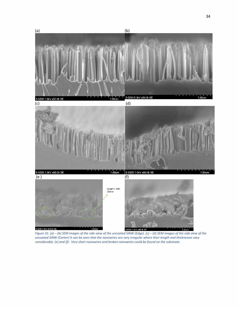
4.1 Uncoated SiNW
Figures 30 below demonstrated the SEM top view image of the uncoated SiNW where some holes
between the nanowires could be seen. Figure 31(a) – (f) were the SEM side view images of the
uncoated SiNW where it can be seen that the nanowires were quite irregular as their length and
thickness vary considerably. From Figure 31(e) and (f), it can be observed that some very short
nanowires, with length between 100 to 200nm, and some broken nanowires, which maybe due to
transportation issues, were found at the bottom of the array. Figure 32(a) was the AFM top view
image of the uncoated SiNW whereas Figure 32(b) was the height profile obtained from the AFM. It
can be seen that the nanowires had length of approximately 800nm.
Figure 30: SEM images of the top view of the uncoated SiNW
34
(a)
(b)
(c)
(d)
(e )
(f)
Figure 31: (a) – (b) SEM images of the side view of the uncoated SiNW (Edge). (c) – (d) SEM images of the side view of the uncoated SiNW (Center) It can be seen that the nanowires are very irregular where their length and thicknesses vary considerably. (e) and (f): Very short nanowires and broken nanowires could be found on the substrate.
35
(a)
(b)
Figure 32: (a) AFM images of the top view of the uncoated SiNW (b) Height profile from AFM showing that the lengths of
the nanowires were approximately 800nm
The lengths of the nanowires were measured to be in the range of 300nm to 1800nm. It should be
noted that the diameter of the NWs varied considerably since the reactions happened very fast
during chemical etching [40]. Area coverage of NW was also determined with the use of the
software, ImageJ, and it is found that the area covered with nanowires was approximately 60-80%.
With all these dimensions, the maximum number of nanowires being indented by the AFM tip
would be approximately 200.
Figure 33 below demonstrated the EDS images of the uncoated SiNW. It is shown that the chemical
composition was mainly silicon with a small amount of silver since silver was a very common catalyst
for chemical etching fabrication of SiNW.
36
(a)
(b)
Figure 33: (a) EDS mapping of the top view of the uncoated SiNW (b) Chemical composition of the uncoated SiNW showing
that it is mostly consisted of silicon. A small amount of silver was detected since silver was a common catalyst of chemical
etching for the fabrication of SiNW
37
4.2 Alumina-coated core shell SiNW
Figure 34 (a) and (b) showed the SEM top view image of the alumina-coated SiNW and the EDS
result respectively. It should be noted that the alumina coating was fabricated by 20 cycles of atomic
layer deposition at 150°C with a thickness of about 2nm. From the SEM top view image, there was
not any significant difference between the surface morphology of the alumina-coated SiNW and the
uncoated SiNW which was expected since the alumina coating was only 2nm. From Figure 34(b), it
can be observed that there was a significant amount of aluminium in addition to silicon. Figure 35(b)
further proved that the alumina coating was uniformly deposited on the SiNW.
(a)
(b)
Figure 34: (a) EDS mapping of the top view of the alumina-coated SiNW (b) Chemical composition of the alumina-coated SiNW showing that the composition was mainly silicon where aluminium concentration increased significantly
38
(a)
(b)
Figure 35: (a) EDS mapping of the side view of the alumina-coated SiNW (b) Aluminium and oxygen were the major compositions, suggesting alumina coating was uniformly deposited along the silicon nanowire.
39
4.3 Polymer-coated SiNW
Figures 36(a) and (b) were the SEM top view image and the chemical compositions of the polymer-
coated SiNW respectively. It should be noted that the polymer coating was fabricated by 10 cycles of
molecular layer deposition at 150°C with a thickness of 5 nm while the precursor gases comprised
trimethylaluminium and glycerol with a repeating unit of Al-(O-CH2-CH2-O)3. It can be seen that
silicon and aluminum were the major compositions of the structure since the core was made of
silicon and trimethylaluminum was one of the precursor gases. The oxygen composition was
significantly higher than that of alumina-coated SiNW which was due to the additional OH groups
from the glycerol precursor gas. Figure 37 proved that the entire core-shell structure was covered
with aluminium, oxygen and carbon which were all the compositions from the two precursor gases.
(a)
(b)
Figure 36: (a)EDS mapping of the top view of the polymer-coated SiNW (b) Chemical composition of the alumina-coated SiNW showing that the composition were mainly silicon and aluminium where the oxygen concentration was higher than that of the alumina-coated SiNW, which was due to the additional OH groups from the glycerol precursor gas.
40
(a)
(b)
Figure 37: EDS mapping of the side view of the polymer-coated SiNW (b) It can be seen that the polymer coating which consisted of aluminum, oxygen and carbon were covering the entire core-shell structure.
41
Chapter 5: Mechanical Testing Protocol Development As mentioned in the Chapter 3, even though standard contact mechanics models, such as the Hertz
model and JKR model, have been widely used to interpret the force vs. indentation depth graph,
they are not the most appropriate model to measure the mechanical properties of the SiNW arrays
samples due to their discrete nature. Therefore, a new protocol has been developed to interpret the
force vs. indentation depth graph where it makes use of the fundamental concept of the Young’s
modulus for uniaxial loading, which is defined as follow [15]:
Young’s Modulus = 𝑆𝑡𝑟𝑒𝑠𝑠
𝑆𝑡𝑟𝑎𝑖𝑛 (5.1)
Figure 38: Young's modulus (as known as modulus of elasticity) can be determined from the slope of a Stress vs. Strain graph [15]
Generally speaking, Young’s modulus is determined from the slope of a stress vs. strain graph for
uniaxial loading in tension or compression. From the AFM used in this experiment, one can easily
obtain the force vs. indentation depth graph. Hence, the only challenge is to convert the force vs.
indentation depth graph into a stress vs. strain graph. Regarding this, it would be appropriate to
divide the mechanical testing protocol into 2 parts: 1) Stress and 2) Strain.
42
5.1 Stress computation
An equation that can be used to relate stress and force is defined as follow:
𝑆𝑡𝑟𝑒𝑠𝑠 =𝐴𝑝𝑝𝑙𝑖𝑒𝑑 𝑓𝑜𝑟𝑐𝑒
𝐶𝑜𝑛𝑡𝑎𝑐𝑡 𝑎𝑟𝑒𝑎 (5.2)
From this equation, it can be seen that two components are needed to compute the stress of the
material under nanoindentation which are the 1) Applied force and 2) Contact area of the two
contacting bodies. In this protocol, it is assumed the stress is increasing uniformly and can be
treated as an average stress. The applied force can be collected automatically from the AFM during
nanoindentation process. However, the contact area cannot be determined directly from the AFM.
Also, the area functions from the Oliver-Pharr model are not very convenient to be used here since
those functions are restricted to particular tip shapes. Thus, a MATLAB code developed by Dr.
Guillaume Colas at the University of Toronto was adopted to compute the contact area (detailed
code is listed in Appendix 8.1). Colas’s code is able to estimate the actual material interacting with
the tip during nanoindentation and thus one can approximate the contact area between the tip and
the sample for any tip shape. It should be noted that due to the discrete nature of the SiNW array
samples under study, the contact area is assumed to be constant during indentation which was
similar to other studies on the measurement of Young’s modulus of nanomaterials arrays [42].
Figures 39-45 demonstrated the steps to construct the stress vs. strain graph. Step 1 was to locate a
spot for nanoindentation and to measure the height of the nanowires as shown in Figure 39. Step 2
was to apply a force to compress the nanowires array. As mentioned in the beginning of this chapter,
10 cycles of indentation were enforced on the same spot where the force applied was 2μN for all
the nanoindentation testing in this experiment.
43
(a)
(b)
Figure 39: (a) A single spot (“X”) is selected to perform nanoindentation (b) The height profile showing the height of the nanowire was 715nm
Step 3 was to determine the indentation depth compressed by the tip. In this experiment, the
indentation depth was determined from the upper portion of the force vs. indentation depth graph
where a sharp change of the slope on the loading curve could be noticed. From Figure 40, it can be
seen that Slope 2 was much steeper than Slope 1, indicating that actual indentation initiated at
Point B where the tip might only be softly scratching the nanowires before it reached Point B. The
indentation depth was the distance between Point B and Point C which was measured to be
20.47nm.
44
Figure 40: Force vs.indentation depth graph obtained directly from the AFM. It can be seen that Slope 2 was much greater than Slope1 and a sharp change of the slope occurred at Point B. Point B would be selected as the origin where the indentation started to happen and BC was the indentation depth
Step 4 required the determination of the contact area between the tip and the nanowires array with
the use of Colas’s code. There are three main input parameters for Colas’s code, including 1) (x,y)
coordinates of the nanoindentation location; 2) Indentation depth and 3) Tip radius. Figure 41
showed the result from the code where the indentation depth and the contact area were 20.47nm
and 2.1667μm2 respectively. However, it should be noted that this contact area was not the actual
contact area and it could be explained by the contact area vs. indentation depth graph (Figure 42)
which was also generated from Colas’s code.
As shown in Figure 42, the tip started compressing the nanowires array when there was a sharp
change in the slope which was Point B. The actual contact area was calculated to be 1.2μm2. Indeed,
the contact area before the sharp change in the slope might indicate that the tip was only softly
scratching the nanowires arrays instead of compressing them. Hence, those area should not be
considered in the final calculation of the contact area. After determining the actual contact area, the
equation 𝑆𝑡𝑟𝑒𝑠𝑠 =𝐴𝑝𝑝𝑙𝑖𝑒𝑑 𝑓𝑜𝑟𝑐𝑒
𝐶𝑜𝑛𝑡𝑎𝑐𝑡 𝑎𝑟𝑒𝑎 could be applied to compute the changes of the stress throughout
the nanoindentation process.
45
Figure 41: Results from Colas's code where the indentation depth was 20.47 nm and the contact area was 2.1667μm
2
Figure 42: Contact area vs. indentation depth graph. The contact area before Point B should not be considered in the determination of the contact area. The actual contact area was 1.2 μm
2
46
5.2 Strain computation
Strain was the second components needs to be determined which can be calculated using the
following equation:
𝑆𝑡𝑟𝑎𝑖𝑛 = 𝑙𝑖−𝑙𝑜
𝑙𝑜 (5.3)
Where li and lo are the final and initial length of the nanowire respectively [15].
li-lo can be seen as the indentation depth which can be collected from the AFM. lo needed to be
measured from the AFM images before and after each of the nanoindentation. In the above case, lo
would be the nanowire height as shown in Figure 39(b) which was 715nm.
5.3 Stress vs. Strain graph
After calculating the stress and strain changes throughout the nanoindentation testing, the stress vs.
strain graph could be established. Figure 43 below demonstrated stress vs. strain graph for one of
the nanoindentation testing for the alumina-coated SiNW.
Figure 43: A stress vs. strain curve for the alumina-coated SiNW at the 10th cycle. The contact area was 1.2μm
2 which was
calculated previously.
The slope of the unloading curve would be one of the mechanical properties being investigated in
our work since this slope revealed the elastic behaviour of the nanowires after compression. Curve-
fitting was applied on the unloading curve to determine the slope. Figure 44 was the stress vs. strain
graph with curve-fitting applied on the unloading curve. It is shown that the stress-strain slope was
89 MPa. It should be noted that it was decided to entitle this measurement as “slope” rather than
“Young’s modulus” because Young’s modulus is used to describe an intrinsic property of a material.
However, as the nanowires would interact with the tip differently during each cycle (for instance
some nanowires might be broken while some may buckle), the contact area would also vary during
each indentation cycle. Therefore, it was more appropriate to name this measurement as slope of
stress-strain graph or stress-strain slope.
47
Figure 44: A stress vs. strain graph for the alumina-coated SiNW at the 10th cycle. By applying curve-fitting on the unloading curve, it was found that the slope of stress-strain graph was 89 MPa.
Apart from the stress-strain slope, energy dissipation was another mechanical property that could
be determined from the stress vs. strain graph. As shown in Figure 45, the area between the loading
and unloading curves was defined as the energy dissipation which was referred to the energy being
lost to surrounding as heat due to plastic deformation. Detailed interpretation of the stress-strain
data would be explained in the next chapter.
Figure 45: Energy dissipation, which was the area between the loading and unloading curves, was calculated to be 0.005 J/cm
3
48
5.4 Limitation of the code
The MATLAB code developed by Colas allowed one to estimate the contact area for any sample and
any tip shape. Yet it should be noted here that the code itself did not consider the force applied to
deform the sample and the determination of the contact area was based on geometry only where
the AFM tip was placed at a certain depth of the nanowire arrays. This is considered to be a
reasonable approach given the discrete nature of the nanowire arrays under study. However, to
obtain a better understanding of the interaction between the sample and the tip, in-situ SEM should
be used in future work.
49
Chapter 6: Mechanical properties of Uncoated Silicon
Nanowires and Core-shell Silicon Nanowires The mechanical testing protocol described in Chapter 5 was applied on all the three nanowires
samples: 1) Uncoated SiNW; 2) Alumina-coated SiNW and 3) Polymer-coated SiNW. A summary of
the samples parameters and testing conditions was included in Appendix 8.2. It is found that the
shapes of the stress vs. strain graphs obtained in this experiment were quite different from the
traditional stress vs. strain graph in a way that the loading and unloading curves were very uneven
(Figure 46(b)). This can be attributed to the fact that all three SiNW array samples consisted of very
irregular nanowires. Since the nanowires were all of different length and thicknesses, it can be
predicted that the number of nanowires being compressed by the AFM tip would be different during
each nanoindentation testing. Also, some nanowires might break while some might buckle (See
schematic Table 2) and hence the loading and unloading curves were not smooth. Detailed images
of the stress vs. strain graphs for all three samples could be found in Appendix 8.3.
(a)
(b)
Figure 46: (a) Traditional stress vs. strain graph consists of very smooth loading and unloading curves [43] (b) It can be found that the loading and unloading curves obtained from the stress vs. strain graphs in our experiments were very uneven.
50
Table 2: Schematic diagram of various sources of energy dissipation of the nanowires during nanoindentation [44]
Sources of energy
dissipation
Sliding Fracture Plastic deformation
Shear
The three SiNW arrays samples have undergone a number of nanoindentation testing where each
testing consisted of 10 cycles of nanoindentation. Three major mechanical properties were studied:
1) Stress-strain slope; 2) Energy dissipation and 3) Straining ability. Section 6.1 described the stress-
strain slope behaviour of the uncoated SiNW whereas section 6.2 discussed the stress-strain slope
for all three samples. Section 6.3 comprised a detailed explanation of the energy dissipation of the
three samples. Section 6.4 explored the straining ability of the different SiNW arrays while section
6.5 included a comparison of the experimental results with computational simulation results.
Before going into the detailed results from our experiment, it would be appropriate to obtain a basic
understanding the mechanical properties of the core and the shell materials of the three samples
since it is expected that the coating material would play a role in changing the properties of the
entire core-shell structure. Table 3 below summarized various mechanical properties that have been
previously reported for silicon (core), alumina (shell) and polymer (shell). These will be used to aid in
the interpretation of the results reported in the following sections.
Table 3: Previously reported mechanical properties of silicon and the two coating materials: alumina and polymer
Young's modulus
(GPa) Friction
coefficient
Bulk silicon
129-187 [15] 0.43 [45]
Alumina 198±8 [46] 0.55-0.82
[47]
Polymer 21±8 [46] n/a
Several notes should be stated here regarding the above mechanical properties. First of all, the
Young’s moduli of the alumina and polymer were obtained from an alumina thin film (fabricated by
atomic layer deposition) and a polymer thin film (fabricated by molecular layer deposition)
respectively [46]. It should be noted that the precursor gases used for molecular layer deposition in
our experiment and the experiments from the references were different. The precursor gases used
in our experiment consisted of trimethylaluminium and glycerol whereas the precursors from the
51
references comprised trimethylaluminium and ethylene glycol. The only difference is that glycerol
contains one more hydroxyl group than ethylene glycol and hence it is still appropriate to study
these references. In addition, the friction coefficients of bulk silicon and alumina were both obtained
by macro-scale ball-on-disc test for the sake of the fairness of the comparison.
6.1 Stress-strain slope of Uncoated SiNW
From Figure 47 below, it can be seen that the largest stress-strain slope of the uncoated SiNW array
was approximately 200MPa. However, there was a huge discrepancy between our results and the
result from those mechanical testing of single nanowire. F. Xu et al. conducted in-situ SEM tensile
test on single SiNW where they found that the Young’s modulus of a single SiNW with 60nm
diameter was about 180GPa which was similar to that of bulk silicon [17]. Yet, our result was indeed
similar to several other studies on carbon nanotubes arrays where the carbon nanotube arrays had
been compressed by triboindenters and nanoindenters [42]. A single carbon nanotube is well-known
for its extremely high Young’s modulus which has a range of 100GPa to 4.15 TPa. However, when
the carbon nanotubes arrays were compressed, it was found that their Young’s moduli were only
0.12MPa to a maximum of 60 MPa [42]. Therefore, it is reasonable to predict that the failure
mechanism of the SiNW arrays might be similar to that of the carbon nanotubes array.
1) Folding of the SiNW and Si substrate (Si-Si) interface and 2) buckling of the nanowires were
believed to be the two main causes of the low stress-strain slope of the uncoated SiNW as compared
to the Young’s modulus of bulk silicon. During indentation, the AFM tip would first contact the top
part of the nanowires and thus the top part was supposed to be compressed. However, it was very
likely that the top part of nanowires would only slide and rotate when they were compressed as
there was no adhesion sticking the nanowires together. Therefore, the bottom part of the nanowire
and the Si-Si interface would in turn bear most of the load. Also, it is likely that the Si-Si interface
was a weak contact point and thus the interface would be prone to breakage and folding, resulting
in a low stress-strain slope as compared to the bulk Si Young’s modulus. Moreover, SiNW were very
likely to buckle when they were compressed where there is a possibility that the both top part and
bottom part (which was close to the Si-Si interface) would buckle. This dual buckling would then
lead to a lower stress-strain slope than the bulk Si Young’s modulus since bulk Si was less prone to
buckling.
52
Figure 47: Relationship between average slope of stress-strain graph of the nanowires and their length. It is seen that alumina-coated SiNW exhibited the highest slope when the nanowires were of the same length. Besides, the stress-strain slope of alumina-coated SiNW was found to decrease with increasing length.
6.2 Stress-strain slope of Uncoated, Alumina-coated and Polymer-coated SiNW
As mentioned in Chapter 2, some researchers have already shown that core-shell single nanowire
not only possessed high Young’s modulus, but it could also limit the growth of the SEI layer which
better conserve the charge capacity and prolong the lifetime of LIB [16]. Therefore, our work here
was to study the stress-strain slope of uncoated and core-shell SiNW arrays to see if the shell
material would also increase the stress-strain slope of the entire array. Besides, as nanoindentation
has been conducted on nanowires with different length, it is possible to study the relationship
between nanowire length and the stress-strain slope. Figure 47 revealed the relationship between
the average stress-strain slope and the nanowire length for all three samples. It should be noted
some data points were removed due to systematic experimental errors that were identified during
analysis (See Appendix 8.4).
From Figure 47, it can be seen that alumina-coated SiNW exhibited the largest stress-strain slope
when the three types of nanowires were compared in the same length. This may be attributed to
the fact that the alumina coating would experience the largest stress and strain as compared to the
silicon core under compression [16]. F. Xu et al. conducted in-situ SEM buckling test and measured
the Young’s modulus of a single ZnO NW, where they found that the Young’s modulus of ZnO NW
was higher than that of a bulk ZnO when the diameters was less than 80nm. They concluded that
the Young’s modulus of the ZnO NW was dominated by the elastic property of the surface as the
surface would experience the largest stress and strain under buckling. Hence the surface atoms
would need to reconstruct themselves and undergo bond contraction to reduce the excessive
surface energy, leading to a higher Young’s modulus. F Xu et al. also conducted another in-situ SEM
tensile test on single SiNW where they found that the Young’s modulus of SiNW would decrease
53
with decreasing diameter. It was concluded that surface effect was still dominating the SiNW where
the oxide layer, which had a lower Young’s modulus than the silicon core, would result in a decrease
of the Young’s modulus of the SiNW when the diameter decreased. In our experiment, it is believed
that surface effect would play a role in altering the stress-strain slope of the nanowire since it can be
deduced that alumina coating would experience the largest stress and thus the interatomic spacing
of coating would decrease. Accordingly, the alumina molecules at the surface would need to
reconstruct themselves to lower the excessive surface energy through bond contraction, meaning
that the elastic properties were dominated by alumina coating. Since alumina coating has a very
high Young’s modulus (Table 1), it can be deduced that the stress-strain slope of the entire alumina-
coated SiNW would become higher.
Furthermore, the rule of mixture might give us an additional clue for the high stress-strain slope of
alumina-coated SiNW even though it did not take surface effect in consideration. Rule of mixtures is
defined as [15]:
Ec= EmVm + EpVp (6.1)
Where E and V are the Young’s modulus and volume fraction respectively, the subscripts c, m and p
refer to composite, matrix and particulate phase respectively.
Using the rule of mixtures equation and combining the Young’s moduli of alumina and polymer in
Table 1, it can be deduced that the stress-strain slope of alumina-coated SiNW would be higher as
the alumina coating itself exhibited very high modulus.
Besides, friction coefficient of the coating material might play a role in changing the stress-strain
slope of the nanowire arrays. From Table 1, it can be seen that the friction coefficient between two
alumina surfaces ranged from 0.55 to 0.82 whereas the friction coefficient between two silicon
dioxide contacts has shown to be approximately 0.43. During nanoindentation, it can be estimated
that SiNWs would slide against each other. Given that the friction coefficient of alumina was greater
than that of silicon oxide, it can be deduced that a larger force would be required to slide the
alumina-coated SiNW, which could also led to a higher stress-strain slope.
Moreover, it is found that the stress-strain slope of alumina-coated SiNW was decreasing with
increasing length. This size effect might be explained by several engineering theories. Firstly,
according to the weakest link theory, it is said that a material with longer length would have a higher
probability of containing a critical defect to cause failure [14]. In other words, the long nanowires
would easily break when they were compressed by the AFM tip which resulted in a lower stress-
strain slope. Secondly, it is expected that the longer nanowires would experience significant buckling
than shorter ones. An equation that relates the force required to induce buckling and the material
length is defined as [48]:
𝑃 =𝜋2𝐸𝐼
𝐿 (6.2)
54
Where P is the critical load to buckle a column, L is the material length, E is the Young’s modulus of
the material, I is the moment of inertia of the cross section.
From this equation, it can be deduced that the longer nanowire are more prone to buckling than the
shorter ones and would give rise to a lower stress-strain slope. However, the stress-strain slope of
polymer-coated SiNW showed an opposite trend which was not conceivable and further research
should be conducted to study the mechanical behavior of the polymer coating.
6.3 Energy dissipation of Uncoated SiNW, Alumina-coated SiNW and Polymer-
coated SiNW During nanoindentation, it is very likely that the nanowires would be compressed which lead to
various sources of energy dissipation. Table 3 demonstrated several types of sources of energy
dissipation. Theoretically speaking, a perfectly elastic material could store 100% of its mechanical
energy into strain energy when it is loaded (either in compression or in tension). The material is then
able to release 100% of the strain energy when the load is removed [43]. However, many materials
would behave elastically at low strain only. When the materials are subjected to high strain, they are
no longer elastic and would deform plastically. Since the area under the loading curve and the
unloading curves represents the energy absorbed and energy released respectively, the difference
between the two curves can be interpreted as the energy lost as heat [43]. Accordingly, the energy
dissipation could be calculated from the area between the loading and unloading curve of a stress vs.
strain graph. Figure 48 below showed the relationship between the average energy dissipation (i.e.
the average energy dissipation of the 10 nanoindentation cycles) and the nanowire length.
Figure 48: Average energy dissipation vs. Nanowire length graph. It can be seen that the energy dissipation was decreasing with increasing nanowire length. Also, nanowires with length below 900nm would deform plastically.
From Figure 48, it can be seen that the energy dissipation was decreasing with increasing nanowire
length for all three samples. In addition, it is observed that the average energy dissipation was very
55
low for all three samples when the nanowire length exceeded 900nm It should be noted that the
energy dissipation of the samples were related to the strain level which was covered in section 6.4.
Therefore, it can be said that all three types of nanowires were deforming elastically when their
length exceeded 900nm whereas they were deforming plastically with length below 900nm.
Moreover, when nanowires with the same length (e.g. 200nm) were compared, it can be seen that
alumina-coated SiNW exhibited the highest energy dissipation while the uncoated SiNW showed the
lowest energy dissipation. Hence, this result suggested that alumina-coated SiNW might contain
more sources of energy dissipation than the other two samples. Interestingly, it was also found that
the energy dissipation of alumina-coated SiNW was decreasing with nanoindentation cycles for
some testing (Appendix 8.5). However, the reason for causing this decreasing trend is still not known
and further studies could be focused on alumina-coated SiNW.
From Figure 49 below, it can be predicted the nanowires would be compressing each other during
lithiation since the nanowires would undergo volume expansion. Therefore, it can be said that
compression would be the dominating mechanism as compared to tension when it came to battery
application. When the nanowires were compressed, there was a likelihood that the nanowires
would buckle. Since the nanowire arrays were made of the same kind of nanowire, the force
required to buckle one single nanowire would be the same for every nanowire on the array.
However, since the nanowires were all of different length and thickness in our samples, it was very
likely that one nanowire would buckle first and then other nanowires would be loaded. As a result,
the nanowires would be shearing. From Figure 48, it can be seen that alumina-coated SiNW
exhibited the highest energy dissipation which suggested that the interface between the alumina
shell and silicon core were likely to be more subjected to shearing as shearing was a source of
energy dissipation.
Figure 49: SiNW would be compressing each other during lithiation. Therefore, it is very likely that the nanowires would be shearing, sliding and deforming upon charging cycles [20]
In addition, it is shown in Table 2 that sliding of the nanowires was also a source of energy
dissipation. In fact, SiNW were very likely to slide against each other during AFM indentation since
the nanowires might buckle and would entangle with one another. Therefore, given that the friction
coefficient of alumina was high (see Table 3), it was possible that the alumina-coated SiNW would
56
slide hard against each other which generated more heat and resulted in a higher energy dissipation
than the other two samples as shown in Figure 48.
6.4 Straining ability of Uncoated SiNW, Alumina-coated SiNW and Polymer-coated
SiNW
Knowing that alumina-coated SiNW exhibited both high stress-strain slope and energy dissipation, it
would be appropriate to compare the three samples to see which one exhibited the greatest
straining ability to resist the volume expansion issue during charging and discharging cycles. Figures
50 and 51 below were the nanowire length vs. strain graph and average energy dissipation vs. strain
graph respectively. From Figure 50, it can be seen that shorter nanowires would strain more than
longer nanowires for all three samples. This is expected as the indentation depth was similar for all
indentation tests performed. This also indicates that shorter nanowires had a higher likelihood of
plastic deformation. Also, when looking at the same nanowire length, e.g. 150nm, it can be found
that alumina-coated SiNW strained the least and the polymer-coated SiNW strained the most, which
agreed with our previous result that alumina-coated were the stiffest material among the three
samples.
Figure 50: Nanowire length vs. strain graph where it can be seen that the shorter the nanowires, the higher is the strain. Besides, alumina-coated SiNW strained the least when the three nanowires were of the same length (e.g. 150nm), suggesting that alumina-coated SiNW was the stiffest among the three samples.
From Figure 51, the energy dissipation was found to increase with increasing strain for all three
samples, where alumina-coated SiNW showed the highest energy dissipation at the same strain
level, suggesting that alumina-coated SiNW were more prone to energy dissipation such as sliding
and shearing.
57
Figure 51: Relationship between average energy dissipation and strain. It can be seen that at the same strain level, e.g. 0.065, alumina-coated SiNW exhibited the highest average energy dissipation.
6.5 Comparison with computational simulation of the mechanical properties of
Uncoated SiNW and Alumina-coated SiNW We have compared our experimental results to Large-scale Atomic/Molecular Massively Parallel
Simulator (LAMMPS) along with Molecular Dynamic (MD) modelling carried out on different types of
SiNW in the research group of Prof. C.V. Singh in the Department of Materials Science and
Engineering at the University of Toronto. In Singh’s study, three types of individual SiNW: 1)
had been pulled to failure under tensile testing at 0K. Even though the testing condition of the
simulation and the dimensions of the nanowires were different from our experimental condition,
some similar trends have been observed. From Figure 52, it can be seen that the alumina-coated
SiNW exhibited the highest ductility among the three nanowires, meaning that alumina-coated
SiNW would experience highest energy dissipation under tension and compression. In other words,
when the alumina-coated SiNW was compressed during nanoindentation, it would lose more energy
that might be due to shearing at the interface, nanowires buckling and sliding, which matched our
experimental result.
58
Figure 52: MD Simulation on the tensile testing of uncoated SiNW and core-shell SiNWs conducted by Ms. Ijya Srivastava in Prof. C.V. Singh’s research group at the University of Toronto. Results showed that at the same strain level, Al2O3-coated SiNW exhibited the largest ductility which implied that Al2O3-coated SiNW had the greatest ability to underdo plastic deformation, leading to a higher energy dissipation under nanoindentation (Figure courtesy of Ijya Srivastava).
6.6 Summary & Conclusion
In this study, three types of nanowires: 1) Uncoated SiNW; 2) Alumina-coated SiNW and 3) Polymer-
coated SiNW, have been investigated regarding their stress-strain slope, energy dissipation and
straining ability with AFM indentation testing. Firstly, it is found that uncoated SiNW possessed a
much lower stress-strain slope than the Young’s modulus of a single Si nanowire which may be due
to the fact the SiNW would buckle during nanoindentation.
Secondly, alumina-coated SiNW has been shown to exhibit the highest stress-strain slope at the
same length and same strain level among the three samples. The high stress-strain slope of alumina-
coated SiNW is believed to be attributed to the fact the alumina coating, which had a very high
Young’s modulus, was dominating the elastic properties of the entire core-shell structure. Also, it is
estimated that the high friction coefficient of alumina would make the sliding between alumina-
coated SiNW more difficult which led to a higher stress-strain slope. Furthermore, it is found that
the stress-strain slope of alumina-coated SiNW decreased with increasing length since longer
nanowires had a higher probability of containing critical defects that lead to fracture and were more
subjected to buckling and as compared to shorter ones.
Thirdly, the energy dissipation of the alumina-coated SiNW is found to be the highest which
indicated that alumina-coated SiNW consisted of more sources to lose energy during
59
nanoindentation. For instance, the alumina shell- silicon core interface might be more prone to
shearing. Besides, the high friction coefficient of the alumina coating suggested that the sliding of
the nanowires under nanoindentation would generate more heat which was also a source of energy
dissipation.
Lastly, a comparison with computational analysis conducted by Prof. C.V. Singh and his research
group at the University of Toronto has been conducted on uncoated SiNW and alumina-coated
SiNW to verify the experimental result where it is found that alumina-coated SiNW was more ductile
than uncoated SiNW, proving that alumina-coated SiNW would lose more energy during
compression and thus show a higher energy dissipation, which matched our experimental result.
All in all, in order to tackle the mechanical issues during charging and discharging cycles, the anode
materials should be stiffer and exhibit higher strain-to-failure. From our results, it is found that short
alumina-coated SiNW would be the most suitable material to replace conventional graphite anode
as alumina-coated SiNW showed the highest stress-strain slope and strain-to-failure among the
three samples.
60
Chapter 7: Conclusion and Future Work
7.1 Conclusion
The objectives of this work were to evaluate the stress-strain slope, energy dissipation and straining
ability of three types of SiNW array samples: 1) Uncoated SiNW; 2) Alumina-coated SiNW and 3)
Polymer-coated SiNW using AFM nanoindentation in order to study the relationship between
structural parameters (including nanowire length and coating materials) and to identify a design
guideline to synthesize core-shell SiNW that can improve the mechanical properties of future LIB
anode and hence the lifetime of LIB.
Prior to conducting AFM nanoindentation, a new mechanical property testing protocol has been
developed since typical contact mechanics models such as the Hertz model, DMT and JKR modes,
which are the most common techniques to interpret AFM results, are subjected to a number of
unrealistic assumptions for the materials under study here. This new protocol made use of the
fundamental concepts of Young’s modulus and can better simulate the contact areas which could
measure the stress-strain slope and the energy dissipation of the three nanowires samples under
nanoindentation more accurately.
Our results showed that alumina-coated SiNW exhibited the highest stress-strain slope at the same
length and same strain level among three samples. It is believed that alumina coating, which
possessed a very high Young’s modulus, was dominating the elastic properties of the entire core-
shell nanowire which gave rise to an increase to the stress-strain slope. In addition, the friction
coefficient of alumina was so high that it would hinder the sliding between alumina-coated SiNW
which meant more force would be required to deform the nanowire and was very likely to result in a
higher stress-strain slope. Furthermore, it is demonstrated that the stress-strain slope of alumina-
coated SiNW decreased with increasing length which is due to the fact that longer nanowires had a
higher probability of containing critical defects and were more subjected to buckling.
It is also found that alumina-coated SiNW exhibited the highest energy dissipation at the same
length and same strain level during nanoindentaton. This is believed to be attributed to the fact that
alumina-coated SiNW were subject to more sources of energy dissipation, such as core-shell
interfacial shearing and hard sliding of the nanowires.
Our experimental result was compared with a computational analysis making use of molecular
dynamics modelling that studied the mechanical behavior of uncoated SiNW and alumina-coated
SiNW. It is shown by the simulation that alumina-coated SiNW demonstrated higher ductility than
uncoated SiNW, implying that alumina-coated SiNW would lose more energy under compression
and would show a higher energy dissipation under nanoindentation, which matched our
experimental result.
61
To summarize, it has long been shown that conventional graphite anodes of LIB are subjected to
several mechanical and electromechanical issues, such as local strain formation, volume expansion,
SEI formation and capacity fading, which greatly deteriorate the LIB performance and lifetime.
Therefore, it is very imperative to develop a new type of anode material that possesses high
stiffness and strain-to-failure to cope with all these issues. From our study, it is shown that short
alumina-coated SiNW would be the most suitable material as it showed the highest stress-strain
slope and energy dissipation during nanoindentation testing.
7.2 Future work
Given the results presented in this work, several future studies should be focused:
1) The study of mechanical properties of polymer coating
It has been shown that the stress-strain slope of polymer-coated SiNW was increasing with
increasing length. However, longer nanowire should be more prone to buckling which would
result in a lower stress-strain slope. Therefore, it is estimated that the polymer coating
might have altered the mechanical properties of the entire core-shell structure. Accordingly,
further studies should be focused on the polymer coating.
2) Stress-strain slope and energy dissipation studies on lithiated nanowires arrays
It has been mentioned that current graphite anodes of LIB are subjected to several
mechanical and electromechanical issues upon charging and discharging cycles. Therefore,
the stress-strain slope, energy dissipation and strain-to-failure of the lithiated nanowires
arrays should also be studied in order to ensure that the use of these nanowires arrays can
potentially improve the mechanical properties of the anodes and hence the performance of
LIB.
3) In-situ SEM studies
Our results were all obtained from AFM and computational simulations where we were able
to measure the mechanical properties, such as stress-strain slope and strain-to-failure, of
the nanowires arrays. However, we were not able to visualize the interaction between the
nanowires and the AFM tips. It is estimated that the nanowires might break and buckle. Yet
using in-situ SEM could allow us to verify our assumptions and ensure that our
measurement is completely accurate. Therefore, in-situ SEM studies are extremely
important in order to prove that the nanowires arrays are applicable in future LIB.
62
Chapter 8: Appendix
8.1 Dr. G. Colas’s MATLAB for the determination of contact area
Table 4: The nanowires length, tip radii and tip materials of each testing
Testing no. Coating NW length (nm) Tip radius(μm) Tip material
1 Uncoated 1000.00 28 Glass
2 Uncoated 1500.00 28 Glass
3 Uncoated 1824.63 28 Glass
4 Uncoated 843.60 20 Borosilikatglas
5 Uncoated 150.42 20 Borosilikatglas
6 Uncoated 278.91 20 Borosilikatglas
7 Uncoated 453.21 20 Borosilikatglas
8 Alumina 1219.00 28 Glass
9 Alumina 899.80 28 Glass
10 Alumina 716.13 20 Borosilikatglas
11 Alumina 333.93 20 Borosilikatglas
12 Alumina 128.81 20 Borosilikatglas
13 Polymer 1590.99 20 Borosilikatglas
14 Polymer 270.00 20 Borosilikatglas
15 Polymer 960.00 20 Borosilikatglas
16 Polymer 509.93 20 Borosilikatglas
17 Polymer 103.09 20 Borosilikatglas
68
8.3 AFM images of nanoindentation from 1st cycle to the 10th cycle
Figure 53, 54, 55 below demonstrated the stress-strain behaviour of uncoated SiNW, alumina-
coated and polymer-coated SiNW.
Figure 53: Stress vs. Strain curve for all 10 cycles of the uncoated SiNW with height of 150.4 nm and their corresponding contact areas and stress-strain slopes during each cycle.
69
Figure 54: Stress vs. Strain for all 10 cycles of the alumina-coated SiNW with length of 128nm and their corresponding contact areas and stress-strain slopes during each cycle.
70
Figure 55: Stress vs. Strain curve for all 10 cycles of the polymer-coated SiNW with length of 103nm and their corresponding contact areas and stress-strain slopes during each cycle.
71
8.4 Data points removal due to systematic experimental errors
Figure 56 : Origin of Figure 47 where two data points, 1 and 2, were circled as outliers.
From Figure 56, two data points were identified as outliers. For point 1, it is found that the AFM tip
was actually indenting the wrong location (Figure 57). For point 2, it is found that the contact area
was halved which maybe due to some nanowires breakage (Figure 58).
(a)
(b)
(c)
(d)
Figure 57: (a) Right before the 1
st nanoindentation test where “X” was the location chosen for nanoindentation (b), (c) and
(d) were the AFM images after the 2nd
, 3rd
and 10th
nanoindentation cycles respectively. It can be seen that the white area (red circles) remained unchanged after the 10
th cycles meaning that it was not compressed by the AFM tip at all. However,
some materials (green circle) were removed which implied that the AFM tip was indenting the wrong spot.
72
(a)
(b)
(c)
(d)
Figure 58: (a) AFM image right before 1
st cycle of nanoindentation where “X” was chosen to be the nanoindentation
location. (b), (c) and (d) were the AFM images after the 2nd
, 3rd
and 10th
nanoindentation cycles respectively where it can be seen that the original white area (red circles) split into half which resulted in a smaller contact area and a higher stress-strain slope. This may be due to the breakage of the nanowires.
73
8.5 Energy dissipation of alumina-coated SiNW
Figure 59: It was found that the energy dissipation of alumina-coated SiNW was decreasing with nanoindentation cycles for several testing
74
Bibliography
[1] B. Scrosati, J. Garche, "Lithium batteries: Status, prospects and future," Journal of Power Sources, vol.
195, pp. 2419-2430, 2010.
[2] Yoshino, A., "Course of development of lihtium ion battery, and future outlook," Nature publishing group,
2013.
[3] X. e. a. Wu, "Rational Design of Anode Materials Based on Group IVA Elements (Si, Ge, Sn) for Lithium-Ion
Batteries," Chem. Asian J., vol. 8, p. 1948 – 1958, 2013.
[4] P. l. M. P. N. P. Verma, "A review of the features and analyses of the solid electrolyte interphase in Li-ion
batteries," Electrochimica Acta, vol. 55, p. 6332–6341, 2010.
[5] McDowell, T et al, "The effect of metallic coatings and crystallinity on the volume expansion of silicon
during electrochemical lithiation/delithiation," Nano Energy, vol. 1, no. 3, pp. 401-410, 2012.
[6] G. Y. N. Nitta, "High-Capacity Anode Materials for Lithium-ion Batteries: Choice of Element and structures
for Active Particles," Part. Part, Syst. Charact, 2013.
[7] "Mineral Commodity Summaries 2015," U.S. Department of the Interior, U.S. Geological Survey,
Washington, DC, 2015.
[8] Goodenough, J et al, "The Li-Ion Rechargeable Battery: A Perspective," J. Am. Chem. Soc., vol. 135, pp.
1167-1176, 2013.
[9] T. e. a. McDowell, "Stable cycling of double-walled silicon nanotube battery anode through solid-
electrolyte interphase control," Nature Nanotechnology, vol. 7, pp. 310-315, 2012.
[10] C.X. Lu, Y. Fan, H.Li, Y.Yang, B.K. Ty, E.Teo, Q. Zhang, "Core-shell CNT-Ni-Si nanowires as a high
performance anode material for lithium ion batteries," Carbon, vol. 63, pp. 54-60, 2013.
[11] A.Kushima, J.Y. Huang, J.Li, "Quantitative Fracture Strength and Plasticity measurements of Lithiated
Silicon Nanowires by In Situ TEM Tensile Experiments," ACS Nano, vol. 6, no. 11, pp. 9425-9432, 2012.
[12] T. B. F. P. G. P. F. M.J. Gordon, "Size Effects in Mechanical deformation and Fracture of Cantilvered Silicon
Nanowires," Nano Letter, vol. 9, no. 2, pp. 525-529, 2009.
[13] C. Cao, A. Reiner, C. Chung, S.H. Chang, I. Kao ,R. V. Kukta, C. S. Korach , "Buckling initiation and
displacement dependence in compression of vertically aligned carbon nanotube arrays," Carbon, vol. 49,
pp. 3190-3199, 2011.
[14] Hertzberg, R.W., Deformation and Fracture Mechanics of Engineering Materials, New Jersey: John Wiley
& Sons, Inc., 1996.
75
[15] W.D. Callister, D.G. Rethwisch, Fundamentals of Materials Science and Engineering: An Integrated
Approach, New Jersey: John Wiley & Sons, Inc., 2008.
[16] Xu, F et al, "Mechanical Properties of ZnO Nanowires Under Different Loading Modes," Nano Res, vol. 3,
pp. 271-280, 2010.
[17] F. Xu et al., "Mechanical Properties of Vapor-Liquid-Solid Synthesized Silicon Nanowires," Nano Letters,
vol. 9, no. 11, pp. 3934-3939, 2009.
[18] T. Ando, K. Sato, M. Shih, T. Yoshioku, Y. Yoshikuwa, T. Kawabata, "Orientation-Dependent Fracture Strain
in Single-Crystal Silicon Beams Under Uniaxial Tensile Conditions," in International Symposium on
Micromechanics and Human Science, Piscataway, NJ, USA, 1997.
[19] Green, M, Fielder, E, Scrosati, B, Wachtler,M, Moreno, J.S., "Structured Silicon Anodes for Lithium Battery
Applications," Electrochemical and Solid-State Letters, vol. 6, no. 5, pp. 75-79, 2003.
[20] J. Graetz, C.C. Ahn, R. Yazami, B. Fultz, "Highly Reversible Lithoum Storage in Nanostructued Silicon,"
Electrochemical and Solid-State Letters, vol. 6, no. 9, pp. 194-197, 2003.
[21] Limmer, S et al., "In Situ Transmission Electron Microscopy Observation of Pulverization of Aluminum
Nanowires and Evolution of the Thin Surface Al2O3 Layers during Lithiation–Delithiation Cycles," Nano
Lett., vol. 11, no. 10, p. 4188–4194, 2011.
[22] George, S., "Atomic Layer Deposition: An Overview," Chem. Rev., vol. 110, pp. 111-131, 2010.
[23] S.M. George, B.H. Lee, B. Yoon, A.I. Abdulagatov, R.A. Hall, "Growth and Properties of Hybrid Organic-
Inorganic Metalcone Films Using Molecular Layer Deposition Techniques," Adv. Funct. Mater., vol. 23, pp.
532-546, 2013.
[24] B. Chen, J. Wang, Q. Gao, Y. Chen, X. Liao, C. Lu, H.H. Tan, Y. Mai, J. Zou, S. P. Ringer, H. Gao, C.Jagadish,
"Strengthening Brittle Semiconductor Nanowires through Stacking Faults: Insights from in Situ Mechanical
Testing," NanoLett., vol. 13, pp. 4349-4373, 2013.
[25] J. Zang, L. Bao, R.A. Webb, X. Li, "Electron Beam Irradiation Stiffens Zinc Tin Oxide Nanowires," NanoLett.,
vol. 11, pp. 4885-4889, 2011.
[26] E. Meyer, H. Hug, R. Bennewitz, Scanning probe microscopy: A Lab on a tip, Berlin; New York: Springe,
2003.
[27] Oliver, R.A., "Atomic Force Microscopy," Department of Material Science & Metallurgy, University of
Cambridge, Cambridge, UK, 2014.
[28] H. B. R.A. Wilson, "Basic Theory: Atomic Force Microscopy (AFM)," Department of Chemistry, Northern
Kentucky University, KY.
[29] H.Chen, "Tribological Properties of Ultrathin Films for MEMS Applications," Univesityof Toronto, Toronto,
76
2014.
[30] J.E. Sader, J.W.M. Chon, P. Mulvaney, "Calibration of rectangular atomic force microscope cantilevers,"
Review of Scientific Instruments, vol. 70, no. 10, pp. 3967-3969, 1999.