Cntrl Using DSP, Lab 2: F28335 & CCSv5 April 2013 B.C. Chang & M.U. Salman, MEM Dept. Drexel Univ. 1/14 MEM800-005 MEM380-006 Control Applications of DSP Lab 2 Project Creating & GPIO – DSP28355 & CCSv5 B.C. Chang and Mishah U. Salman Department of Mechanical Engineering & Mechanics Drexel University 2013
Transcript
Cntrl Using DSP, Lab 2: F28335 & CCSv5 April 2013
B.C. Chang & M.U. Salman, MEM Dept. Drexel Univ. 1/14
MEM800-005 MEM380-006
Control Applications of DSP
Lab 2
Project Creating & GPIO – DSP28355 & CCSv5
B.C. Chang and Mishah U. Salman
Department of Mechanical Engineering & Mechanics
Drexel University
2013
Cntrl Using DSP, Lab 2: F28335 & CCSv5 April 2013
B.C. Chang & M.U. Salman, MEM Dept. Drexel Univ. 2/14
1. Objective
The objective of this lab is to get the students more familiar with the CCSv5.2 and to learn another fundamental peripheral, GPIO (general-purpose input/output). In this lab, you will learn how to directly create new projects from scratch on CCSv5.2 without using the existing projects of previous CCS version and migration like you did in Lab 1. You will create two projects from scratch in the CCSv5.2 environment: 2s_hello and 2s_createproj_epwm. GPIO pins are used for general-purpose binary input/output operations. Most of the computer peripheral signals are multiplexed with GPIO signals. This enables the user to use a pin as GPIO if the peripheral signal or function is not used. On reset, GPIO pins are configured as inputs. The user can individually program each pin for GPIO mode or peripheral signal mode. In this lab, you will also migrate two existing CCSv3.3 projects to CCSv5.2: 2s_gpio_toggle_delay_A and 2s_gpio_toggle_int_B. The two GPIO projects will be employed to generate digital signals and send them to GPIO6 (P8:#16) and GPIO7 (P8:#21) pins as outputs. In 2s_gpio_toggle_delay_A, the timing of the toggled output is controlled by a “for loop” with time delay, while in 2s_gpio_toggle_int_B, interrupts are used to control the timing. 2. Creating a New Simple Project: 2s_hello
In this section, you will learn how to create a simple CCSv5 project from scratch. After the project 2s_hello is created, you can debug (including compiling to covert the source code to the machine code), load the machine code to the F28335 DSP chip, and run the program. The function of this simple program is just to print a message like “Hello World!” on the output device of choice.
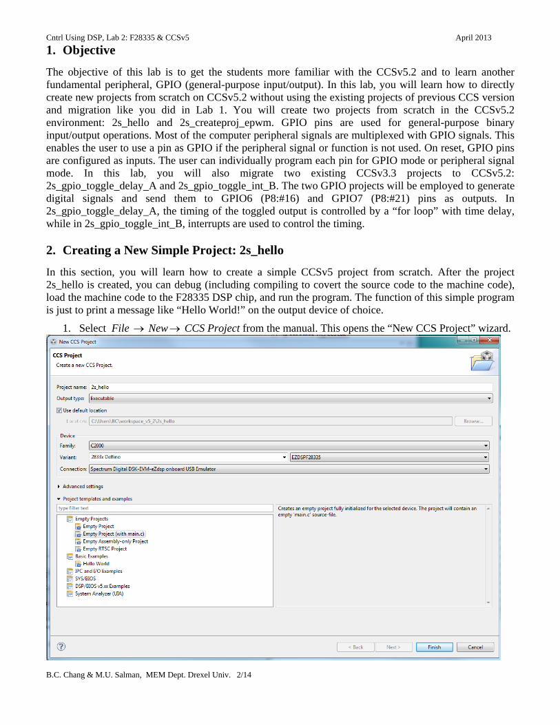
1. Select File New CCS Project from the manual. This opens the “New CCS Project” wizard.
Cntrl Using DSP, Lab 2: F28335 & CCSv5 April 2013
B.C. Chang & M.U. Salman, MEM Dept. Drexel Univ. 3/14
2. In the “Project Name” field, type the new project name: 2s_hello. 3. In the “Output type”, select “Executable”. 4. Check the small box to choose “Use default location” to keep the new project files in your
workspace folder. 5. Select “C2000” in the “Family” field. 6. In the “Variant” field: select “2833x Delfino” and “EZDSPF28335”. 7. In the “Connection” field, select “Spectrum Digital DSK-EVM-eZdsp onboard USB Emulator”. 8. The “Advanced settings” section is minimized by default. 9. Expand the “Project templates and examples” section. Then select “Empty Project (with main.c)” 10. Press the “Finish” button. 11. You will see the new project 2s_hello appears on the Project Explorer View window, and a new
folder 2s_hello is created in your workspace folder.
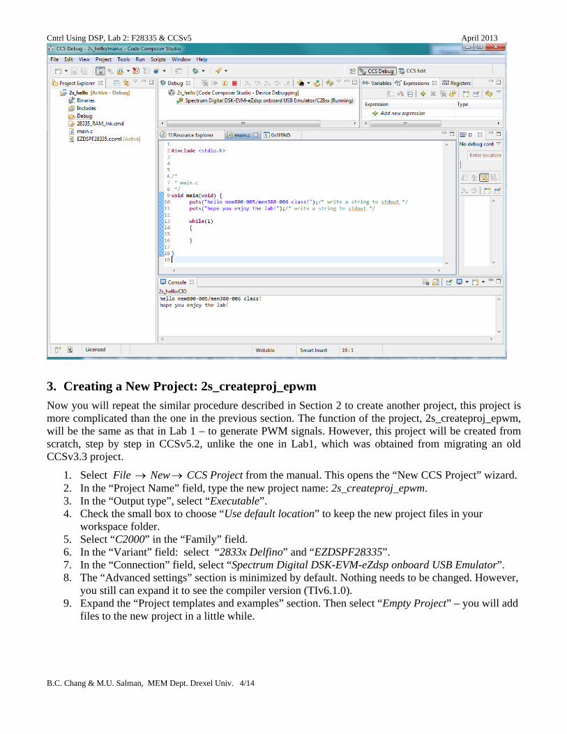
12. Insert the following C code inside the braces of the void main(void) program:
puts("hello mem800‐005/mem380‐006 class!");/* write a string to stdout */ puts("hope you enjoy the lab!");/* write a string to stdout */ while(1) { }
13. Debug, load, and run the program, and you’ll see
hello mem800‐005/mem380‐006 class! hope you enjoy the lab!
appear on the Console View window.
Cntrl Using DSP, Lab 2: F28335 & CCSv5 April 2013
B.C. Chang & M.U. Salman, MEM Dept. Drexel Univ. 4/14
3. Creating a New Project: 2s_createproj_epwm
Now you will repeat the similar procedure described in Section 2 to create another project, this project is more complicated than the one in the previous section. The function of the project, 2s_createproj_epwm, will be the same as that in Lab 1 – to generate PWM signals. However, this project will be created from scratch, step by step in CCSv5.2, unlike the one in Lab1, which was obtained from migrating an old CCSv3.3 project.
1. Select File New CCS Project from the manual. This opens the “New CCS Project” wizard. 2. In the “Project Name” field, type the new project name: 2s_createproj_epwm. 3. In the “Output type”, select “Executable”. 4. Check the small box to choose “Use default location” to keep the new project files in your
workspace folder. 5. Select “C2000” in the “Family” field. 6. In the “Variant” field: select “2833x Delfino” and “EZDSPF28335”. 7. In the “Connection” field, select “Spectrum Digital DSK-EVM-eZdsp onboard USB Emulator”. 8. The “Advanced settings” section is minimized by default. Nothing needs to be changed. However,
you still can expand it to see the compiler version (TIv6.1.0). 9. Expand the “Project templates and examples” section. Then select “Empty Project” – you will add
files to the new project in a little while.
Cntrl Using DSP, Lab 2: F28335 & CCSv5 April 2013
B.C. Chang & M.U. Salman, MEM Dept. Drexel Univ. 5/14
10. Press the “Finish” button. 11. You will see the new project 2s_createproj_epwm appears on the Project Explorer View window,
and a new folder 2s_createproj_epwm is created in your workspace folder. Note that the target configuration file, EZDSPF28335.ccxml, which is automatically generated, and the linker command file, 28335_RAM_lnk.cmd, and a header files folder, C:/ti/ccsv5/tools/compiler/c2000_6.1.0/include, are already included in the project. Next, you’ll add more files and headers to complete the project creation.
12. Add files to the project: Select Project Add Files, and look in the folder C:\tidcs\c28\DSP2833x\v131\CntrlDSP \2s_createproj_epwm_orig and double click 2s_createproj_epwm.c to add it to the project.
13. Repeat step 12 to look in C:\tidcs\c28\DSP2833x\v131\DSP2833x_common\source and select DSP2833x_CpuTimers.c, DSP2833x_DefaultIsr.c, DSP2833x_EPwm.c, DSP2833x_PieCtrl.c, DSP2833x_PieVect.c, and DSP2833x_SysCtrl.c.
14. Also go to C:\tidcs\c28\DSP2833x\v131\DSP2833x_headers\source to add DSP2833x_GlobalVariableDefs.c to the project.
15. Repeat to find the assembly source files: DSP2833x_ADC_cal.asm, DSP2833x_CodeStartBranch.asm, and DSP2833x_usDelay.asm, in C:\tidcs\c28\DSP2833x\v131\DSP2833x_common\source and add them to the project.
Cntrl Using DSP, Lab 2: F28335 & CCSv5 April 2013
B.C. Chang & M.U. Salman, MEM Dept. Drexel Univ. 6/14
16. Repeat to add the Linker Command File DSP2833x_Headers_nonBIOS.cmd to the project from C:\tidcs\c28\DSP2833x\v131\DSP2833x_headers\cmd.
17. Look at the Project Explorer View window to make sure there are two .cmd file, eight .c files, and three .asm files in the project folder 2s_createproj_epwm.
18. Next, you’ll add three more header file folders to the project. Select Project Properties
Include Options from the manual. In the lower-right pane of the “Properties for 2s_createproj_epwm” window, click the green arrow icon (Add) to pop up the “Add directory path”.
19. Press the button “File System …” to search for the directory C:\ti\xdais_7_21_01_07\packages\ti\xdais then click the “OK” button .
Cntrl Using DSP, Lab 2: F28335 & CCSv5 April 2013
B.C. Chang & M.U. Salman, MEM Dept. Drexel Univ. 7/14
20. Repeat Step 19 again to add the following two header file folders to the project:
21. Now the project is ready for debug and compiling. If there is no error and a xxx.out file is
generated, load the object file to the DSP chip and run the program. 22. Check if it is functioning as that in the project, 1s_epwm, in Lab 1.
4. Connections for GPIO
Connect the eZdsp board to the USB port of the PC DO NOT OPEN THE SOCKET on the board to avoid damaging the DSP chip inside.
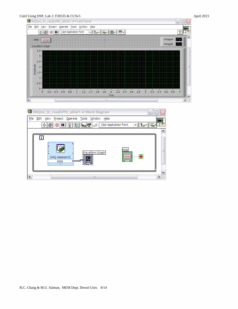
Connect the DAQ box to PC and Build a LabVIEW VI Connect the NI USB-6211 (DAQ) box to PC via USB cable and connect AI0, AI1, and AIGND to eZdsp Pins P8: #16, #21 and P8: #19, respectively. A simple LabVIEW VI will be needed to observe the GPIO signals.
NI USB-6211 (DAQ) TI F28335 eZdsp
AI0 P8: #16 AI1 P8: #21
AIGND P8: #19
Cntrl Using DSP, Lab 2: F28335 & CCSv5 April 2013
B.C. Chang & M.U. Salman, MEM Dept. Drexel Univ. 8/14
Cntrl Using DSP, Lab 2: F28335 & CCSv5 April 2013
B.C. Chang & M.U. Salman, MEM Dept. Drexel Univ. 9/14
Cntrl Using DSP, Lab 2: F28335 & CCSv5 April 2013
B.C. Chang & M.U. Salman, MEM Dept. Drexel Univ. 10/14
5. Generation of GPIO Signals with Timing Controlled by a Time Delay
5A. Migrate the CCSv3.3 Project 2s_gpio_toggle_delay_A to CCSv5.2
The CCSv3.3 project, 2s_gpio_toggle_delay_A.pjt, together with the associated C program, 2s_gpio_toggle_delay_A.c and a gel file 2s_gpio_toggle_delay_A.gel can be found in the folder 2s_gpio_toggle_delay_A_orig, which is inside the directory C:\tidcs\c28\DSP2833x\v131\CntrlDSP.
You can employ the migration procedure you learned in Lab 1 to migrate the existing CCSv3.3 Project 2s_gpio_toggle_delay_A to CCSv5.2. You also have an option to follow the procedure in Section 3 to directly create the new CCSv5.2 project from scratch based on 2s_gpio_toggle_delay_A.c.
5B. Debug, Build and Run the Newly Migrated Project 2s_gpio_toggle_delay_A 1. Select the project by clicking the 2s_gpio_toggle_delay_A in the "Project Explorer" view. 2. Click on the green bug (debug button) on the tool bar. 3. The debugging process will do the following:
(i) Save all open files in the project selected (ii) Build the selected project and create an executable file 2s_gpio_toggle_delay_A.out, which
appears in the folder Debug (iii) Automatically switched the CCS Debug perspective
4. The "Debug" view is now visible. (i) This view should always be open. Do not close it. If it is accidently closed, you can open it again
using the "view debug" menu item. (ii) It allows you to connect the target device and control it (run, suspend, etc.)
5. Select "Run Load Load Program" to load the executable file 2s_gpio_toggle_delay_A.out to the target device.
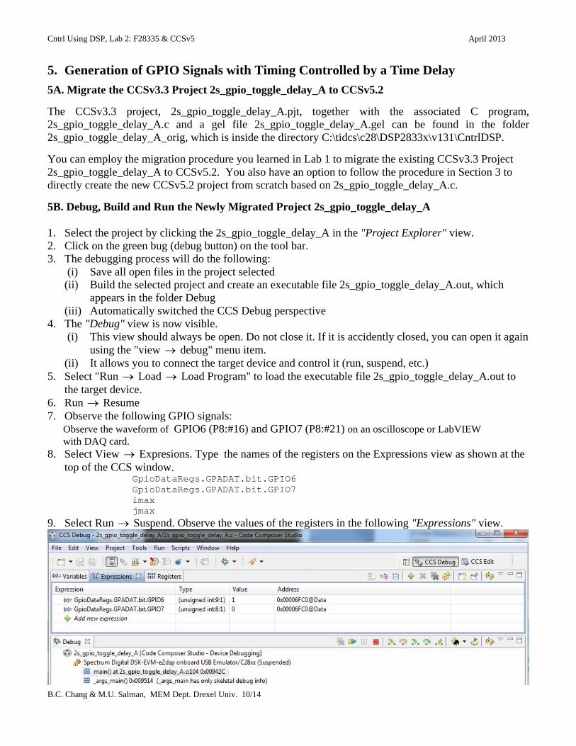
6. Run Resume 7. Observe the following GPIO signals: Observe the waveform of GPIO6 (P8:#16) and GPIO7 (P8:#21) on an oscilloscope or LabVIEW with DAQ card. 8. Select View Expresions. Type the names of the registers on the Expressions view as shown at the
top of the CCS window. GpioDataRegs.GPADAT.bit.GPIO6 GpioDataRegs.GPADAT.bit.GPIO7 imax jmax 9. Select Run Suspend. Observe the values of the registers in the following "Expressions" view.
Cntrl Using DSP, Lab 2: F28335 & CCSv5 April 2013
B.C. Chang & M.U. Salman, MEM Dept. Drexel Univ. 11/14
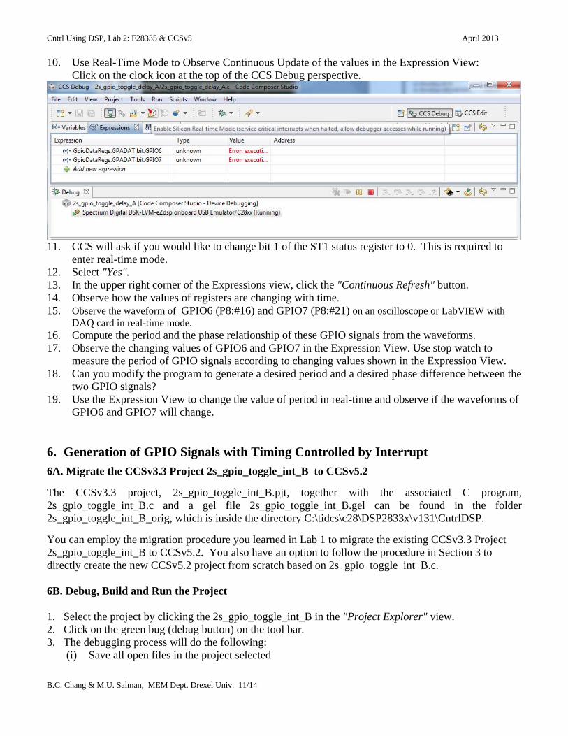
10. Use Real-Time Mode to Observe Continuous Update of the values in the Expression View: Click on the clock icon at the top of the CCS Debug perspective.
11. CCS will ask if you would like to change bit 1 of the ST1 status register to 0. This is required to
enter real-time mode. 12. Select "Yes". 13. In the upper right corner of the Expressions view, click the "Continuous Refresh" button. 14. Observe how the values of registers are changing with time. 15. Observe the waveform of GPIO6 (P8:#16) and GPIO7 (P8:#21) on an oscilloscope or LabVIEW with
DAQ card in real-time mode. 16. Compute the period and the phase relationship of these GPIO signals from the waveforms. 17. Observe the changing values of GPIO6 and GPIO7 in the Expression View. Use stop watch to
measure the period of GPIO signals according to changing values shown in the Expression View. 18. Can you modify the program to generate a desired period and a desired phase difference between the
two GPIO signals? 19. Use the Expression View to change the value of period in real-time and observe if the waveforms of
GPIO6 and GPIO7 will change. 6. Generation of GPIO Signals with Timing Controlled by Interrupt
6A. Migrate the CCSv3.3 Project 2s_gpio_toggle_int_B to CCSv5.2
The CCSv3.3 project, 2s_gpio_toggle_int_B.pjt, together with the associated C program, 2s_gpio_toggle_int_B.c and a gel file 2s_gpio_toggle_int_B.gel can be found in the folder 2s_gpio_toggle_int_B_orig, which is inside the directory C:\tidcs\c28\DSP2833x\v131\CntrlDSP.
You can employ the migration procedure you learned in Lab 1 to migrate the existing CCSv3.3 Project 2s_gpio_toggle_int_B to CCSv5.2. You also have an option to follow the procedure in Section 3 to directly create the new CCSv5.2 project from scratch based on 2s_gpio_toggle_int_B.c. 6B. Debug, Build and Run the Project 1. Select the project by clicking the 2s_gpio_toggle_int_B in the "Project Explorer" view. 2. Click on the green bug (debug button) on the tool bar. 3. The debugging process will do the following:
(i) Save all open files in the project selected
Cntrl Using DSP, Lab 2: F28335 & CCSv5 April 2013
B.C. Chang & M.U. Salman, MEM Dept. Drexel Univ. 12/14
(ii) Build the selected project and create an executable file 2s_gpio_toggle_int_B.out, which appears in the folder Debug
(iii) Automatically switched the CCS Debug perspective. 4. The "Debug" view is now visible.
(i) This view should always be open. Do not close it. If it is accidently closed, you can open it again using the "view debug" menu item.
(ii) It allows you to connect the target device and control it (run, suspend, etc.) 5. Select "Run Load Load Program" to load the executable file 2s_gpio_toggle_int_B.out to the
target device. 6. Run Resume 7. Observe the following GPIO signals: Observe the waveform of GPIO6 (P8:#16) and GPIO7 (P8:#21) on an oscilloscope or LabVIEW with DAQ card. 8. Select View Expresions. Type the names of the registers on the Expressions view as shown at the
top of the CCS window. GpioDataRegs.GPADAT.bit.GPIO6 GpioDataRegs.GPADAT.bit.GPIO7 CpuTimer0.InterruptCount Period 9. Select Run Suspend. Observe the values of the registers in the following "Expressions" view. 10. Use Real-Time Mode to Observe Continuous Update of the values in the Expression View: Click on the clock icon at the top of the CCS Debug perspective. 11. CCS will ask if you would like to change bit 1 of the ST1 status register to 0. This is required to
enter real-time mode. 12. Select "Yes". 13. In the upper right corner of the Expressions view, click the "Continuous Refresh" button. 14. Observe how the values of registers are changing with time. 15. Observe the waveform of GPIO6 (P8:#16) and GPIO7 (P8:#21) on an oscilloscope or LabVIEW with
DAQ card in real-time mode. 16. Compute the period and the phase relationship of these GPIO signals from the waveforms. 17. Observe the changing values of GPIO6 and GPIO7 in the Expression View. Use stop watch to
measure the period of GPIO signals according to changing values shown in the Expression View. 18. Can you modify the program to generate a desired period and a desired phase difference between the
two GPIO signals? 7. Discussions
What approach was used in the 2s_gpio_toggle_delay_A program to achieve timing control? Does this approach provide precise timing control? Does this approach use CPU time efficiently? Explain the reasoning behind your answers in detail. What approach was used in the 2s_ gpio_toggle_int_B program to achieve timing control? Does this approach provide precise timing control? Does this approach use CPU time efficiently? Explain the reasoning behind your answers in detail. Explain what interrupt means in the 2s_ gpio_toggle_int_B program.
Cntrl Using DSP, Lab 2: F28335 & CCSv5 April 2013
B.C. Chang & M.U. Salman, MEM Dept. Drexel Univ. 13/14
Appendix A: //============================================================================= // // FILE: 2s_gpio_toggle_delay_A.c // // // This program is modified from Example_2833xGpioToggle.c, // // by B.C. Chang, Chirag Jagadish, Mishah U. Salman, Drexel Univ. // on March 28, 2010 // // This program requires the // DSP2833x/DSP2823x C/C++ Header Files V1.31, released by TI on August 4, 2009. // //========================================================================== // // Toggle GPIO PORT pins, // GpioDataRegs.GPADAT.bit.GPIO6, // GpioDataRegs.GPADAT.bit.GPIO7, // using a for loop to control the timing // // // Use Expression View to observe // // GpioDataRegs.GPADAT.bit.GPIO6 // GpioDataRegs.GPADAT.bit.GPIO7 // imax // jmax // // The pins of these GPIO ports can be observed using // Oscilloscope. // //==========================================================================
Appendix B: //============================================================================= // // FILE: 2s_gpio_toggle_int_B.c // // // This program is modified from Example_2833xCpuTimer.c, // // by B.C. Chang, Mishah U. Salman, Drexel Univ. // on March 28, 2010 // // This program requires the // DSP2833x/DSP2823x C/C++ Header Files V1.31, released by TI on August 4, 2009. // //========================================================================== // // Toggle GPIO PORT pins, // GpioDataRegs.GPADAT.bit.GPIO6, // GpioDataRegs.GPADAT.bit.GPIO7, // using interrupt to control the timing // // Use Expression View to observe // CpuTimer0.InterruptCount // GpioDataRegs.GPADAT.bit.GPIO6 // GpioDataRegs.GPFDAT.bit.GPIO7
Cntrl Using DSP, Lab 2: F28335 & CCSv5 April 2013
B.C. Chang & M.U. Salman, MEM Dept. Drexel Univ. 14/14
// period // // The pins of these GPIO ports can be observed using // Oscilloscope. // //==========================================================================


![TMS320x2833x, 2823x Enhanced Capture [ECAP] Module ...changbc/dspcntrl_F28335/eCAP...•4 x 32-bit time-stamp capture registers (CAP1-CAP4) •4-stage sequencer (Modulo4 counter) that](https://static.documents.pub/doc/80x56/611334e7f6928c34f648df63/tms320x2833x-2823x-enhanced-capture-ecap-module-changbcdspcntrlf28335ecap.jpg)


