31
1 Memory Devices CEN433 King Saud University Dr. Mohammed Amer Arafah

1
Memory Devices
CEN433
King Saud University
Dr. Mohammed Amer Arafah
Mohammed Amer Arafah2CEN433 - King Saud University
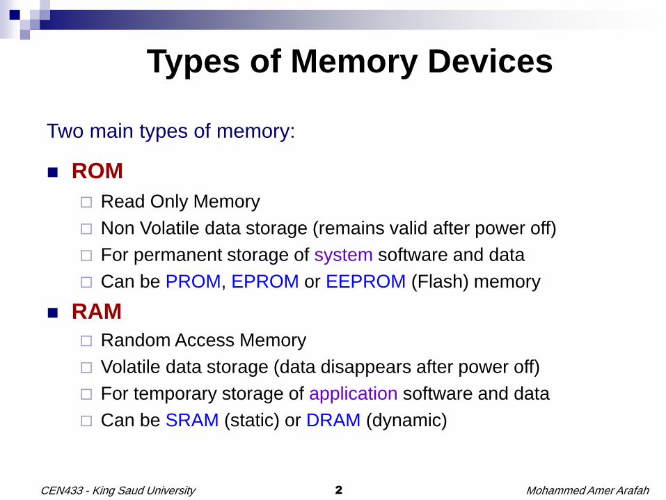
Types of Memory Devices
Two main types of memory:
ROM
Read Only Memory
Non Volatile data storage (remains valid after power off)
For permanent storage of system software and data
Can be PROM, EPROM or EEPROM (Flash) memory
RAM
Random Access Memory
Volatile data storage (data disappears after power off)
For temporary storage of application software and data
Can be SRAM (static) or DRAM (dynamic)

Mohammed Amer Arafah3CEN433 - King Saud University
Memory Pin Connections
Address Inputs: Select the required location in
memory.
Address lines are numbered from A0 to as many as required to address all memory locations
Example: 12-bit address: A0-A11
212 = 4K memory locations
Today’s memory devices range in capacities upto 1G locations (30 address lines)
Example: 4K memory: 12 bits: 000H-FFFH. e.g. from 40000H to 40FFFH.
Output
Or
Input/Output
Connections
O0
O1
O2...
OM
A0
A1
A2......
AN
CE/
Address
Connections
OE/
WE/
Memory
Decode this
part for CS

Mohammed Amer Arafah4CEN433 - King Saud University
Memory Pin Connections
Data Inputs/Outputs (RAM)
Data Outputs (ROM)
Number of lines = width of data
storage, usually a byte D0-D7
(M=7)
Wider processor data buses use
multiple of such byte-wide
memory devices, e.g. 64-bit
8 x 8-bit devices
Sometimes the total memory
capacity is expressed in bits, e.g.
a 64K x 8-bit = 512 Kbit
Output
Or
Input/Output
Connections
O0
O1
O2...
OM
A0
A1
A2......
AN
CE/
Address
Connections
OE/
WE/
Memory

Mohammed Amer Arafah5CEN433 - King Saud University
Memory Pin Connections
Control Inputs: Chip Enable (CE/), or Chip Select
(CS/), or simply Select (S/): Select the memory device for READ or WRITE operations.
In addition, Indicate whether you want to READ or Write:
READ: Enable device output for READ operations (only operation on ROMs) using OE/ or G/. If not enabled, output will be Hi-Z (floating)
WRITE: (for RAM only) Enable device for writing using WE/ input. Should not be active simultaneously with #OE
Some memory devices have one READ/WRITE control: R/#W
Output
Or
Input/Output
Connections
O0
O1
O2...
OM
A0
A1
A2......
AN
CE/
Address
Connections
OE/
WE/
Memory

Mohammed Amer Arafah6CEN433 - King Saud University
Memory Organization
Many memory device are 8-bits in width.
A 4K x 8 memory contains 4,096 (4K) memory locations, each containing 8-bits
A 16M x 4 memory has 16 M memory locations, each being 4-bits wide
A 512M byte DDR* memory card for your PC is organized as a 64M x 8 bytes. It contains eight 64M x 8 bit memory devices
___________________________________
* Double Data Rate, SDRAM with data transfer at both clock edges

Mohammed Amer Arafah7CEN433 - King Saud University
Read Only Memory Devices
Many Types of read only memory: (Programming getting easier…)
ROM Device permanently programmed in factory by manufacturer
Must be large number (10,000 pieces) to justify cost
Once manufactured, can not be erased or reprogrammed
PROM Programmable ROM (Programmed once)
When number of devices is too small to justify high factory programming cost
Programmed in a PROM programmer that burns fuse kinks
Once programmed, can not be erased for reprogramming
Changes? Throw away and program another one!
Mohammed Amer Arafah8CEN433 - King Saud University
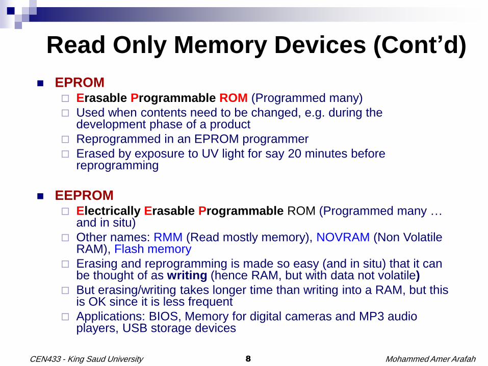
Read Only Memory Devices (Cont’d)
EPROM Erasable Programmable ROM (Programmed many)
Used when contents need to be changed, e.g. during the development phase of a product
Reprogrammed in an EPROM programmer
Erased by exposure to UV light for say 20 minutes before reprogramming
EEPROM Electrically Erasable Programmable ROM (Programmed many …
and in situ)
Other names: RMM (Read mostly memory), NOVRAM (Non Volatile RAM), Flash memory
Erasing and reprogramming is made so easy (and in situ) that it can be thought of as writing (hence RAM, but with data not volatile)
But erasing/writing takes longer time than writing into a RAM, but this is OK since it is less frequent
Applications: BIOS, Memory for digital cameras and MP3 audio players, USB storage devices

Mohammed Amer Arafah9CEN433 - King Saud University
EPROM
2K x 8 read only memory
1 bit + 10 bits = 11 Address inputs
8 Data outputs
Members of the 27XXXX family:
- 2704 : 512 x 8
- 2708 : 1K x 8
- 2716 : 2K x 8
- 2732 : 4K x 8
- 2764 : 8K x 8
- 27128 : 16K x 8
- 27256 : 32K x 8
- 27512 : 64K x 8
- 271024 : 128K x 8
= Memory capacity
in K bits
2716
Address
Data
Ctrl
Mohammed Amer Arafah10CEN433 - King Saud University
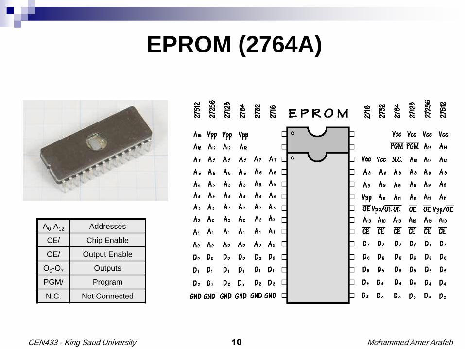
EPROM (2764A)
A0-A12 Addresses
CE/ Chip Enable
OE/ Output Enable
O0-O7 Outputs
PGM/ Program
N.C. Not Connected
Mohammed Amer Arafah11CEN433 - King Saud University
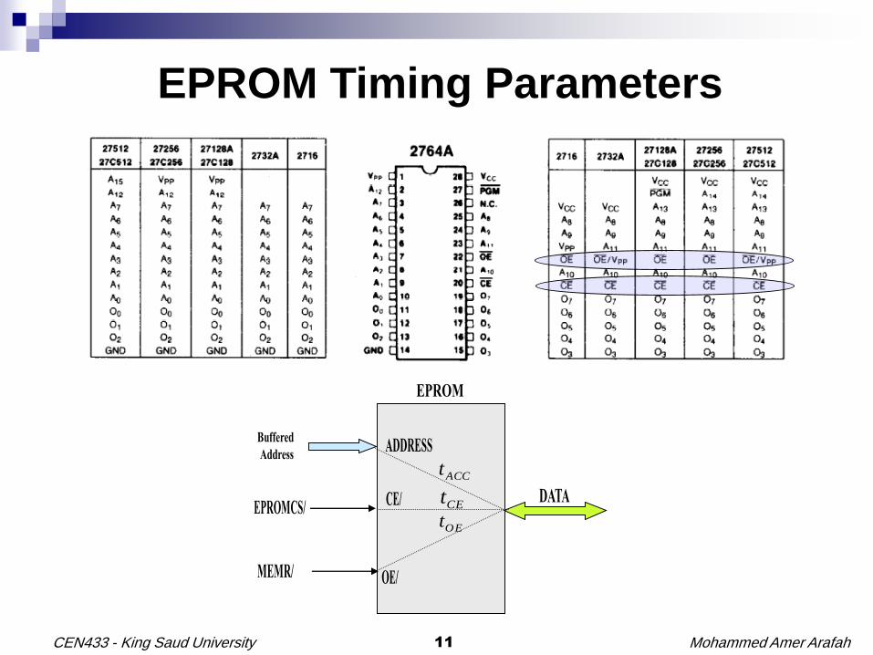
EPROM Timing Parameters
ACCt
OEtCEt

Mohammed Amer Arafah12CEN433 - King Saud University
EPROM Timing Parameters (2764A )

Mohammed Amer Arafah13CEN433 - King Saud University
EPROM Timing Parameters (2764A )

Mohammed Amer Arafah14CEN433 - King Saud University
Example: Interfacing EPROM to 8088-2

Mohammed Amer Arafah15CEN433 - King Saud University
Example: Interfacing EPROM to 8088-2
nsTCLRL 10010 nsTCLRH 8010
nsTCLCL 500125 nsTCLCH 68 nsTCHCL 44
nsTCLAV 6010 nsTCLAZ 5010 nsTDVCL 20 nsTCLDX 10
nsTCLLH 50 nsT CHLL 55
25774_ 100 LSENABLEOUTPUT tnsT +
LATCHAddressBuffered tnsT + 60_
DECODERLATCHSELECTCHIP ttnsT ++ 60_

Mohammed Amer Arafah16CEN433 - King Saud University
Example: Interfacing EPROM to 8088-2}ttt100ns t, ttt60ns , ttMAX{60nsUTEPROM_OUTP OE74LS244ORT1CEDecoderLATCHACCLATCH +++++++++
)ttt100ns t, ttt60ns , ttMAX{60nstto_8088_Avaiable_Data OE74LS244ORT1CEDecoderLATCHACCLATCH74LS245 ++++++++++
nst LS 524574
nsTDVCL 20 nsTCLDX 10

Mohammed Amer Arafah17CEN433 - King Saud University
RAM Memory Devices
Writing is needed more often than with EEPROMs
should be easier and faster.
Two main types of RAM: Static RAM
Dynamic RAM

Mohammed Amer Arafah18CEN433 - King Saud University
Static RAM (SRAM)
A relatively complex cell circuit (several transistors per bit storage)
That is why static RAM devices are more expensive and are typically smaller in capacity compared to dynamic RAM
(A given # of transistors available on a chip gives fewer memory locations)
Faster than dynamic RAMs, speeds down to 1 ns access time are now possible
Used for high speed cache memories
It is rarely the case that a large computer RAM uses only static memory type
Mohammed Amer Arafah19CEN433 - King Saud University
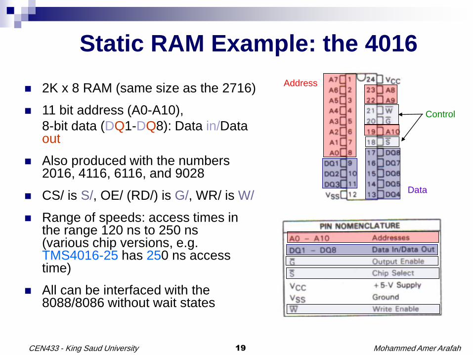
Static RAM Example: the 4016
2K x 8 RAM (same size as the 2716)
11 bit address (A0-A10),
8-bit data (DQ1-DQ8): Data in/Dataout
Also produced with the numbers 2016, 4116, 6116, and 9028
CS/ is S/, OE/ (RD/) is G/, WR/ is W/
Range of speeds: access times in the range 120 ns to 250 ns (various chip versions, e.g. TMS4016-25 has 250 ns access time)
All can be interfaced with the 8088/8086 without wait states
Address
Data
Control

Mohammed Amer Arafah20CEN433 - King Saud University
Static RAM Example: the 4016
Timing Waveform of Read Cycle
Mohammed Amer Arafah21CEN433 - King Saud University
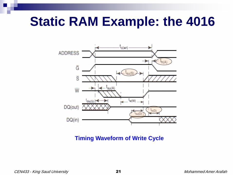
Static RAM Example: the 4016
Timing Waveform of Write Cycle

Mohammed Amer Arafah22CEN433 - King Saud University
Dynamic RAM (DRAM) Unlike static RAM, data is store as a voltage (charge) across a capacitor
Charge of course leaks with time, and data needs to be refreshed (re-written) every
say 2-4 ms
Recent devices usually organized as XX K x 1 bit, largest 1G x 1
Advantages:
Simpler cell circuit
Larger capacities
While Largest SRAM 8 Mbits,
Largest DRAM 1024 Mbits
Lower cost than SRAM
Disadvantages:
Slower access times (e.g. 20 ns vs 1 ns)
Needs refreshing: e.g. every 4 ms max (added complexity)
But not that bad!:
Occurs during normal reads and writes. Also special hidden refresh cycles
occurring simultaneously with other memory accesses (cycle stealing). Dedicated
DRAM refresh controller chips available.
Large storage capacity large address inputs large number of chip pins
required Need for chip pin multiplexing (added complexity)
Mohammed Amer Arafah23CEN433 - King Saud University
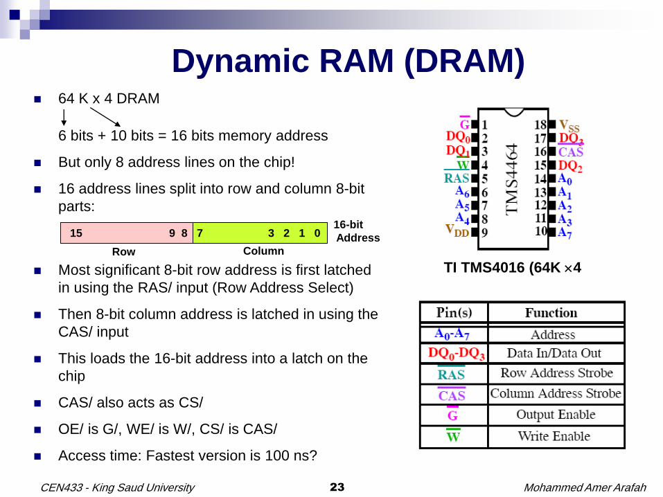
Dynamic RAM (DRAM) 64 K x 4 DRAM
6 bits + 10 bits = 16 bits memory address
But only 8 address lines on the chip!
16 address lines split into row and column 8-bit
parts:
Most significant 8-bit row address is first latched
in using the RAS/ input (Row Address Select)
Then 8-bit column address is latched in using the
CAS/ input
This loads the 16-bit address into a latch on the
chip
CAS/ also acts as CS/
OE/ is G/, WE/ is W/, CS/ is CAS/
Access time: Fastest version is 100 ns?
15 9 8 7 3 2 1 0
Row Column
16-bit
Address
TI TMS4016 (64K 4
Mohammed Amer Arafah24CEN433 - King Saud University
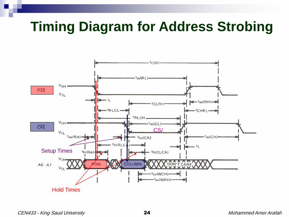
Timing Diagram for Address Strobing
Setup Times
Hold Times
CS/

Mohammed Amer Arafah25CEN433 - King Saud University
Multiplexing the Row/Column AddressA0-A7: 8-bit Column
Address (LS)
A8-A15: 8-bit Row
Address (MS)
8-bit Muxed Address
+ Row Strobe
To 4464 DRAM chip
S = 1 (Row)
74157 Data Multiplexers
2 x (4 x 2-to-1 MUXs)
Select Input
S = 0 (Column))
16-bit Full
Address
From mP
8 address
Inputs to chip
Carry row then
Column address
Selector
Row Strobe
We still require
A CAS/ Strobe
MUX Delay
MUX
Select Row
Address
Select Column
Address
MUX delay > Required Hold
time for row address
RAS/ can be used as a
selector I/P for the MUX and
also as input to the DRAM to
strobe row address in.
RAS/ signal select the row
then the Column address &
its falling edge strobes in the
row address

Mohammed Amer Arafah26CEN433 - King Saud University
Internal Structure of a DRAM
4 data bits from the 4 sections
2 bits of address
Select
Column
8
Select
Row

Mohammed Amer Arafah27CEN433 - King Saud University
Internal Structure of a DRAM 4 sections of 256 x 256 bits each
Each section is addressed by 8 bits of rows and 8 bits for columns
Remaining 2 address bits select the section addressed
Row and column addresses are common to all 4 sections
A whole row of 4 x 256 = 1024 bits is addressed simultaneously (Speeds up refreshing)
The 4 data bits in the addressed column in the 4 sections are addressed simultaneously
Only the bit from the required section is selected by the remaining 2 address bits using MUX3

Mohammed Amer Arafah28CEN433 - King Saud University
DRAM Memory Refreshing
When a row is accessed in a refresh cycle, all memory cells on that row are
refreshed
This means that we need only 256 refresh operations to refresh all the 256K x
1 DRAM above
To refresh the whole memory at the minimum rate of once every 4 ms, we
need to do a refresh cycle every 4 ms/256 = 15.6 ms
If a refresh cycle needs a bus cycle (4T with the 8088/86), the % of bus
cycles lost for refreshing an 8088/86 running at a clock speed of 5 MHz is:
= 4 x 0.2 ms / 15.6 ms = 5.1% (not bad … for the cost saving we achieve using dynamic RAM)
For a Pentium 4 with a clock cycle of 3 GHz and a bus/instruction cycle of 1T,
this % is:
= 1 x 0.33 ns / 15.6 ms = 0.2% (i.e. the penalty for DRAM refreshing is much more tolerable
with modern, faster processors)
15.6 ms
0.8 ms…
4 ms (Refresh whole memory chip)
Only 256 Refresh operations
Cover all the memory
15.6 ms

Mohammed Amer Arafah29CEN433 - King Saud University
Refresh Cycle RAS/ only refresh cycles
RAS/ strobes a row address indicating the row of bits to be accessed for refreshing
This row address is not a full memory address and can be generated by a small on-chip counter (e.g. 8-bits for the 256 rows in the 256K x 1 DRAM described)
The row cells read are fed back for re-writing into the same locations to fulfill refresh requirements
The timing Diagram of the RAS/ refresh cycle for the TMS4464 DRAM

Mohammed Amer Arafah30CEN433 - King Saud University
Internal Structure of a DRAM EDO (Extended Data Output) Memory
All 256 bits of the row from the selected section are saved in latches on the memory chip. So this data will be ready for future access without experiencing the slow memory access time again
Such locations are close to the already accessed data, and are likely to be accessed soon (locality principle)
Improves system performance by 15-25%
SDRAM (Synchronous Dynamic RAM) Memory Memory runs synchronously to the system bus clock, e.g. at 100-133-200 MHz
Burst (block) Transfers Burst transfers of say 4 x 64-bit numbers between the processor and the
memory. First number experiences normal wait states, but 2nd, 3rd, and 4th
transfers suffer no wait states, thus improving average access time.
DDR (Double Data Rate) Memory Data Transferred at double the SDRAM rate by using the two edges of the clock
This does not exactly double the data transfer rate due to access time limitations
Combinations exist, e.g. DDR SDRAM
Mohammed Amer Arafah31CEN433 - King Saud University
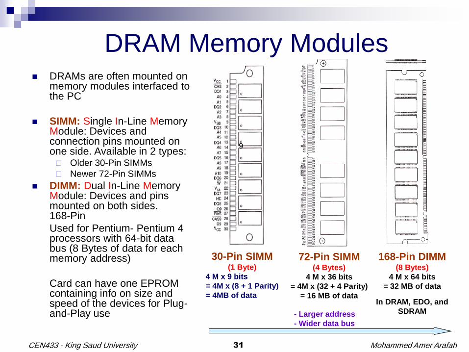
DRAM Memory Modules
9
30-Pin SIMM(1 Byte)
4 M x 9 bits
= 4M x (8 + 1 Parity)
= 4MB of data
72-Pin SIMM(4 Bytes)
4 M x 36 bits
= 4M x (32 + 4 Parity)
= 16 MB of data
- Larger address
- Wider data bus
168-Pin DIMM(8 Bytes)
4 M x 64 bits
= 32 MB of data
In DRAM, EDO, and
SDRAM
DRAMs are often mounted on memory modules interfaced to the PC
SIMM: Single In-Line Memory Module: Devices and connection pins mounted on one side. Available in 2 types: Older 30-Pin SIMMs
Newer 72-Pin SIMMs
DIMM: Dual In-Line Memory Module: Devices and pins mounted on both sides. 168-Pin
Used for Pentium- Pentium 4 processors with 64-bit data bus (8 Bytes of data for each memory address)
Card can have one EPROM containing info on size and speed of the devices for Plug-and-Play use


