Memory Management in Modern Computers • One of the biggest problems facing modern computer designers is
that of providing large amounts of high speed memory. • This is a problem that has evolved over the last 25-30 years. • Earlier in the history of computing, most processors were
relatively slow compared to the speed of available memories (Except for bulk storage mechanical memories, i.e., disks and drums).
• Especially in the early days of the personal computer, the CPU was relatively slow compared to early electronic memories.
• The speed of random-access memory was not an issue; the biggest problem was just getting enough memory, period (early PC’s with large memories had 256-512 Kbytes)!
Erik Jonsson School of Engineering and Computer Science
• Over the last two+ decades, central processor chips have caught up with and passed DRAM speed dramatically.
• Example: current CPU speed is 3-4.5 GHz, depending on the processor type, and should increase somewhat, although manufacturers are now abandoning the “speed race” in favor of multiple processors.
• On the other hand, practical bus speed for CPU memory is about 1-1.8 GHz currently, and this is for “high performance” memory; “common” bus speeds are still no more than half that.
• The CPU performance edge over memory is on the order of 3-4, and much more than that on systems with the more common bus speeds.
Erik Jonsson School of Engineering and Computer Science
The Memory Speed/Cost Dilemma • There are further problem facing the modern computer
designer: – Users need very high memory speeds to improve performance
(for example, in graphical computing, games, video editing). – At the same time there is also great demand for maximum
memory capacity by many users (PC’s do not just manipulate text any more; complex graphics, video games, movie editing and animation all require enormous amounts of both DRAM and bulk storage (hard drives [HDD’s]).
• However, there is a conflict in these requirements: – Fast memories are very expensive. – High-capacity, cheap memories (esp. HDD’s) are very slow.
Erik Jonsson School of Engineering and Computer Science
• The computer designer of today is therefore faced with a problem that is not easy to solve: – There must be enough high-speed memory available to avoid
slowing down the processing rate of current CPU’s. – There must be sufficient DRAM to avoid the deadly “disk
access” (i.e., having to go to the HDD to get program or data material), at least very often, since HDD access is very slow.
– There must be enough bulk memory (HDD) for all storage needs, and accessing this memory and transferring it to DRAM/other memory must be as painless as possible.
– The cost must be reasonable.
Erik Jonsson School of Engineering and Computer Science
• The current approach to memory management : – CPU has a large register complement, which allows more data in the
CPU at a time and improves performance. – Very-high-speed D flip-flop arrays, called cache, hold currently
executing program segments. There are two kinds: • L1/L2 cache – On CPU chip, adjacent to ALU. ~ 64 Kbytes, very fast. • L3 cache – Center of CPU chip. ~ 15+ Mbyte, very fast.
– High-speed electronic memory (“DRAM,” up to 64 Gbytes, fast) provides capacity for programs currently in process.
– Bulk storage memory (disk drives, ~0.3-2+ TByte, slow but cheap) holds complete programs and “near-term” archives.
– Slower memories such as CD’s and DVD’s for long-term storage.
Erik Jonsson School of Engineering and Computer Science
Types of Memory • As we have just seen, even in the everyday PC, the use of
sophisticated memory management is common. • This means that there are four kinds of memory in the modern PC
or workstation computer: Registers, cache, DRAM, and the disk or HDD (or SSM). And this does not count CD’s, DVD’s, Zip drives, thumb drives (flash EPROM), or floppy disks!
• The challenge to the computer engineer is to mesh the first five storage media and to make the use of them “transparent” – that is, invisible to the user, who will appear to have massive amounts of high-speed, cheap memory available to solve any problem.
• Before we discuss how to manage this extremely challenging engineering problem, we will discuss the types of memory that are used and learn a little about them.
Erik Jonsson School of Engineering and Computer Science
• We already know that registers are simply collections of D FF’s. • Most CPU’s today contain many registers, (e.g. the R-2000’s 32). • Registers are inside the CPU, adjacent to the ALU, so their speed
is basically that of the CPU (in fact, they determine ALU speed).
D FF 32-Bit Reg. Register Block
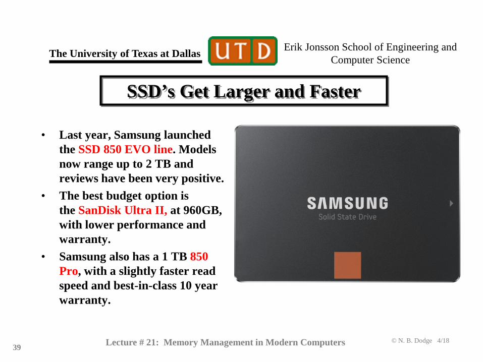
D
C
Q
R
Erik Jonsson School of Engineering and Computer Science
Random-Access Electronic Memory • Random-access memories (RAM) make up the “working memory”
of most computers. • These memories are referred to as “random-access” because the
entire array of memory is immediately available to be used; any single byte in the memory may be loaded or stored (“randomly accessed”) in the same amount of time.
• There are two primary types of RAM: Static RAM (SRAM), and dynamic RAM (DRAM). Both SRAM and DRAM are used in modern computers such as the PC.
• SRAM is used in what are referred to as caches – small, very-high-speed memories that are physically close to the CPU.
• DRAM, though very fast, is slower than SRAM, but because it is inexpensive, it is the primary memory in most personal computing systems.
Erik Jonsson School of Engineering and Computer Science
L1 Cache • L1 cache (“level 1 cache”) is SRAM memory that is very close to
the CPU. For example, it is next to the ALU in most processors. • L1 cache is basically sets of D FF’s – but many more than in the
CPU register block. • For example, a typical register block might have 16-32 registers of
4 or 8 bytes each for a total of 64-128 bytes of storage. The Intel L1 Core i7 cache, on the other hand, has 64 Kbytes (32K instruction, 32K data)– the equivalent of ~ 500,000 flip-flops.
• Access speed of L1 cache is slower, however, due to the complex arrangement of data buses which is necessary to access specific bytes in the L1 memory array. It is typically about 1/2-1/3 as fast as CPU registers in terms of load/store cycle.
Erik Jonsson School of Engineering and Computer Science
• As you saw on the previous slide, in terms of memory structure, cache has regressed. Modern computer chips have separate instruction and data caches!
D FF 32-Bit Reg. L1 Cache
D
C
Q
R
Erik Jonsson School of Engineering and Computer Science
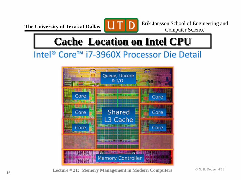
L3 Cache • In modern multicore processors, the cores share the L3
cache, which is typically 8-12 Mbyte. • As L1 cache is slower than the register block, and L2 is
slower than L1, L3 cache is slower still, though much faster than DRAM. The reason is that the L3 cache is yet even farther away from the CPU, though still on the chip.
• To minimize the degradation in memory speed, the CPU’s are typically clustered around the L3 cache, as shown in the picture of the Core i7 chip (upcoming).
Lecture # 21: Memory Management in Modern Computers
Erik Jonsson School of Engineering and Computer Science
Why Not More Cache? • The question arises: If cache memory is so great, why
isn’t all computer memory fast cache? • Answer: Cache memory has two major problems:
– It consumes huge amounts of power compared to DRAM memory (a flip-flop has about sixteen transistors; a DRAM cell uses only one).
– This means if more cache were used, the cost of a computer (think PC) would go up dramatically, due to the cost of extra power to run it, and cost of cooling the computer!
– Also, cache is much more expensive than DRAM (5:1 or more).
• For that reason, DRAM memory is an excellent compromise solution to fast storage problems.
Erik Jonsson School of Engineering and Computer Science
DRAM Memory • The term DRAM stands for “dynamic random-access memory”
(pronounced “D-ram,” not “dram”). This means that the title above is actually redundant!
• DRAM is electronic memory that is capable of very fast access (load or store), but is not as fast as cache. One exception is “Rambus” memory, a special DRAM memory whose manufacturer has announced cache-speed products (up to 7.2 GHz!). It is very expensive, however.
• The simple construction of DRAM makes it ideal in modern, workstation-based computing, where most users have their own computer system (PC, Mac, Sun, etc.).
• DRAM consists of a simple charge-storage device (stored charge = “1”), with a switch to store/test the charge. Only a single transistor is required for a DRAM bit cell.
Erik Jonsson School of Engineering and Computer Science
• The term “dynamic” in DRAM is due to the fact that the memory is not truly a flip-flop; it is not static. DRAM “remembers” a 1 by storing charge on a capacitor.
• Capacitors, however, are not perfect storage elements – the charge leaks off after a short time. Thus the DRAM element is “dynamic” – its memory lifetime is limited and it must have its memory refreshed periodically.
• On the next several slides, we explore the way DRAM is constructed and the odd way that it must be treated to be sure that it retains its memory.
Erik Jonsson School of Engineering and Computer Science
To “write logic 1 data” to a DRAM cell, a voltage is applied to the word line, which turns the transistor on (it is like an “electronic switch”). If a voltage V is applied to the bit line, current flows into the capacitor and charges it, creating a “logic 1.”
Bit line
Word line
CMOS transistor
Ground
Bit line
Word line
CMOS transistor
Capacitor charges
Ground
+V (= logic “1”)
Current
+
+V (= logic “1”) turns on transistor
0V (= logic “0”)
Current
Capacitor discharges
0
+V (= logic “1”) turns on transistor
To “write logic 0 data” to a DRAM cell, a voltage is applied to the word line, which turns the transistor on (once again, like an “electronic switch”). Now, if 0 volts (“ground”) is applied to the bit line, current flows out of the capacitor and discharges it, creating a “logic 0.”
Erik Jonsson School of Engineering and Computer Science
To “read,” or sense the value of the DRAM cell, the word line once again has a voltage applied to it, which turns on the transistor. If the capacitor is charged, current flows OUT of the transistor, and this current is sensed and amplified, showing that a “1” is present. If the capacitor is discharged, no current flows, so that the sensing element determines that a logic 0 is present.
Bit line
Word line
CMOS transistor
Ground
Bit line
Word line
CMOS transistor
Capacitor charged
Ground
logic “1” sensed
Current
+
+V (= logic “1”) turns on transistor
logic “0” sensed
No current flow
Capacitor has no charge
0
+V (= logic “1”) turns on transistor
Read 1 memory cycle. Read 0 memory cycle.
Erik Jonsson School of Engineering and Computer Science
• The refresh cycle occurs after a logic 1 read or periodically if the memory cell is not accessed. The refresh cycle is typically every few milliseconds. Obviously if the cell is a 0, it is not recharged.
Bit line
Word line
CMOS transistor
Ground
Bit line
Word line
CMOS transistor
Capacitor discharges
Ground
Logic “1” read (or sensed in refresh cycle) by draining capacitor
Current
+→0
Word line activated
Capacitor recharged
0→+
Word line reactivated
Read 1 memory cycle or refresh cycle logic “1” detect.
Logic “1” rewritten by applying +V to bit line
Read or refresh cycle logic “1” rewrite.
Current
Erik Jonsson School of Engineering and Computer Science
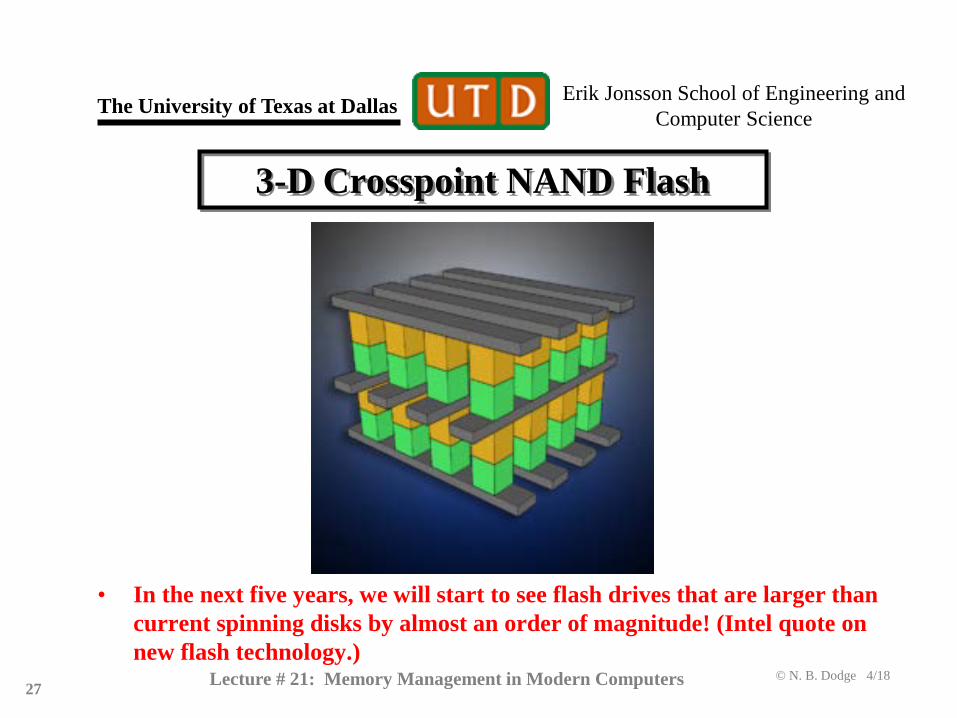
• In the next five years, we will start to see flash drives that are larger than current spinning disks by almost an order of magnitude! (Intel quote on new flash technology.)
Lecture # 21: Memory Management in Modern Computers
Erik Jonsson School of Engineering and Computer Science
1. Rank these memories by speed: L2 cache, DRAM, L1 cache, registers, and hard disk drives.
2. A DRAM memory chip is accessed and a bit read out. The bit that is read is a 1. What happens now?
3. That same memory bit is then left “alone” (i.e., not accessed by its addressing mechanism for either read or write) for several milliseconds. What happens next?
Erik Jonsson School of Engineering and Computer Science
1. (This will help with the Test #3 bonus homework) – Registers in the computer are adjacent to the ALU, L1 is on-chip, L2 is nearby, and DRAM and HDD are farther away from the CPU. Thus the speed ranking is registers, L1, L2, DRAM, HDD.
2. The 1 data is erased by the read, so that the 1 is immediately rewritten after it is read.
3. The capacitor begins to lose charge (the “1”) and so it is rewritten periodically.
Lecture # 21: Memory Management in Modern Computers
Erik Jonsson School of Engineering and Computer Science
Bulk Storage (Disk Storage or HDD) • Electromechanical data storage is normally not random-access like
SRAM or DRAM. • This means that data cannot normally be accessed in arbitrary
order, but must be loaded or stored according to rules, which generally have to do with positioning a recording mechanism over the correct location in an expanse of recording media prior to being able to perform the memory access.
• That is, the correct segment of data must be located (normally by mechanically moving a recording head) before it can be read.
• This load/store operation is particularly time-consuming, because it involves mechanical movement rather than simply electronic switching.
Erik Jonsson School of Engineering and Computer Science
• The HDD stores data on a rotating disk coated with magnetic material.
• A magnetic coil is used to record each one and zero. Current in the coil generates a magnetic field, which magnetizes material in the HDD surface. One direction of current writes a 1, the other a 0.
• When the coil is later positioned over the disk to read, the opposite-polarity 1’s and 0’s cause back-and-forth current flow according to whether a 1 or 0 is present. In this way, the data is detected.
Rotation
Aluminum disk coated with magnetic material
Current flow Magnetic field lines (direction depends on current flow)
Strong, concentrated magnetic field
Erik Jonsson School of Engineering and Computer Science
The HDD is usually packaged in a metal case. Higher-quality units are typically packaged in an aluminum casting, or similar rigid container, which provides stability and better data integrity.
Erik Jonsson School of Engineering and Computer Science
• The latency (“time to get/store data”) of a HDD is given by the formula:
latency = seek time + rotational delay + transfer time + controller delay Where: – Seek time = time for the positioning arm to move the head from its
present track to the track where the load/store data is located. – Rotational time = time for the requested sector to rotate underneath
the read/write head after the head is positioned over the track. – Transfer time = time for data transfer from disk to main memory. – Controller delay = time to set up transfer in the HDD electronic
interface.
Erik Jonsson School of Engineering and Computer Science
• Other storage media include CD’s, DVD’s and “thumb drives.” • Most of these storage units are removable media. • Floppy disks, hard drives, Zip drives, and tapes are magnetic media. • The CD-ROM and the DVD use optical recording/reading involving
a laser beam to record and read data. They are relatively slow. • The “thumb drive” uses electronic memory called EPROM
(“erasable, programmable read-only memory”), and is a true solid-state memory. These drives were the first “SSD’s.”
• Very fast EPROM’s (SSD’s) are beginning to be available for fast bulk storage, replacing HDD’s on laptops. They are relatively expensive.
Erik Jonsson School of Engineering and Computer Science
The Memory Hierarchy • We have described a number of memory devices which
are useful for storing and reading computer data. • All of these (other than archival types) are used in a
mix on the modern computer for real-time storage and retrieval of data.
• Since SRAMs – the best data storage media if not so power-hungry and costly – cannot be used exclusively, a mix of L1 and L2 cache, DRAM, and HDDs make up the “memory hierarchy” of most computers.
• The trick is to design a mix of these types which will give the highest performance for a reasonable price.
Erik Jonsson School of Engineering and Computer Science
Arrangement of the Memory Hierarchy • Memory arrangements make use of the fact that
programs exhibit two common behaviors: – Temporal locality – Recently-used code and data is often
reused (e.g., a loop program continues to use the same steps). – Spatial locality – Recently-accessed data items are usually close
to other recently-accessed (or about-to-be-accessed) data items.
• Modern schemes use a “shuffling” methodology that moves data from slower storage media to faster media.
• Higher-speed memories are also placed closer to the CPU, since memory access also depends on the proximity of the storage element; electronic signals propagate at about 33 ps/cm.
Erik Jonsson School of Engineering and Computer Science
• As mentioned previously, the key to modern computer performance is not the CPU – CPU performance has far-outstripped the speed of most computer memories.
• The key is the use of cache. The secret of today’s high-performance PC’s and workstations is the design of an architecture that allows maximum use of DRAM and HDD (cheap) plus just enough SRAM cache (expensive and power-consuming), thus enabling the CPU to realize most of its performance advantage.
• The method used is the “shuffling” technique alluded to two slides back. This method uses a very high speed, complex arrangement to constantly move program and data content from slower to faster memory as the CPU executes a process.
Erik Jonsson School of Engineering and Computer Science
• Cache designers make use of the principles of temporal and spatial locality to assure that the most-probably needed instructions and data are available to the computer in cache (to speed execution).
• Special hardware is designed to manage cache content with the goal of forecasting upcoming instructions and data required by the processor during program execution and moving it from slower DRAM into cache.
• This hardware has two special goals: (1) examining the currently-executing process and predicting instruction and data need, and (2) moving the required information from DRAM to cache in a timely manner to foresee that anticipated need.
Erik Jonsson School of Engineering and Computer Science
Looking for Data/Instructions in the Cache • Clearly the purpose of cache management is to make sure that ALL
upcoming instructions and data are in the cache. • This brings up two questions: (1) how does the processor know that data
is in the cache, and (2) if it is NOT there, how does the processor get it and what sort of performance penalty is there?
• There are several ways in which the cache can be assigned DRAM memory correspondence. The simplest is direct mapping, in which each block of memory in cache is assigned to some number of DRAM locations.
• When a program needs a particular DRAM location to be loaded, it goes to the corresponding cache location to get the data. This leads to further complications, in that now we need “validity indicators” for each cache location. This is because since each cache block is assigned to several memory blocks in DRAM, the program needs to know if the right data is available in cache at the time it is needed.
Erik Jonsson School of Engineering and Computer Science
Looking for Data (2) • If the correct data is not in cache, the hardware memory manager
declares a “cache miss.” This means that the program must be delayed for several clock cycles while the required instruction or data is moved from DRAM to cache.
• We see that a cache miss is highly undesirable, since it can substantially slow down the program.
• A key part of cache memory management, then, is to minimize the cache misses, which correspondingly increases the speed of execution of a program.
• There are a number of clever and effective cache management designs, which dramatically reduce cache misses and improve computer performance. They are, however, beyond the scope of EE 2310.
Erik Jonsson School of Engineering and Computer Science
Cache management HW includes subsystems to predict usage and move data or instructions from DRAM to cache as appropriate. A “cache miss” initiates DRAM access for transfer to cache.
CPU
Registers
L1 Cache
Single CPU
L2 Cache DRAM HDD L3
Cache
Chip Boundary
Erik Jonsson School of Engineering and Computer Science
Summary • Modern memory management maximizes the speed of
computer processing while keeping system cost reasonable for the user.
• This approach uses a small amount of very fast SRAM cache memory which are physically near the computer, a substantial amount of DRAM, which is still very fast, as the main “working memory,” and HDD or flash memory for large program storage.
• Effective, (but complex) hardware and software have been developed to manage this memory hierarchy and maximize its effectiveness.
Erik Jonsson School of Engineering and Computer Science
1. Each small area of cache (say, 1K byte) represents a much larger area (say, 1 Mbyte) in DRAM. If an instruction, for example, is supposed to reside in a given Mbyte of DRAM, the corresponding cache extent is searched. Assume that, according to the validity indicator, the correct instruction is NOT in cache. What now?
2. Give simple definitions of the principles of temporal and spatial locality.
Erik Jonsson School of Engineering and Computer Science
1. The CPU must wait until the correct instruction can be retrieved from DRAM.
2. “If the data or instruction was used recently, it might be used again soon.” “If the data or instruction was from a particular area of memory, other data/instructions from that area will probably be used.”
Lecture # 21: Memory Management in Modern Computers
Erik Jonsson School of Engineering and Computer Science
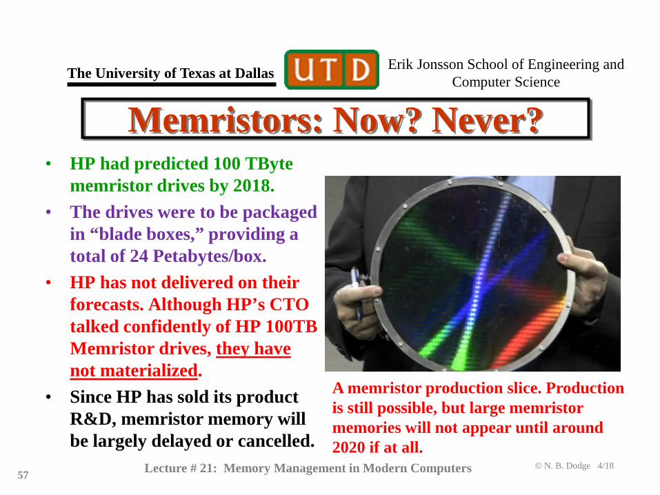
Memory • In 2008, a completely new kind of circuit element (that
was predicted in 1971), the memristor, was developed. • Memristor circuit elements can retain a state (i.e.,
memory) even when power is off. They could eventually replace flash EPROM, and perhaps DRAM. Thousand Gbyte main memories are possible.
• Memristors remember multiple states (not just ones and zeros). Thus a memristor memory might eventually “remember” like a human neuron, leading to neural-type processors in the long term.
Erik Jonsson School of Engineering and Computer Science
tunneling resistance that depends on the relative magnetization of ferromagnetic electrodes. Early devices sold by Everspin, but IBM and Samsung, among others, are also said to be researching MRAM (as of 12/17).
• Resistive RAM (ReRAM) – Varies resistance according to applied voltage. Nonvolatile, low power, high density. Production cost and reliability are problems. SanDisk is working on this technology, and HP is a partner. Progress on this technology appears to be accelerating as of the end of 2017.
Lecture # 21: Memory Management in Modern Computers
Erik Jonsson School of Engineering and Computer Science
The CPU • Intel and AMD abandoned the GHz race in CPU’s
years ago. In the early 2000’s, Intel stated a goal of a 10 GHz CPU by 2010—which clearly didn’t happen.
• Multiple CPU’s became the performance enhancer. The standard is now 4- to 10- core CPU’s, with the new Intel Core i9 at even larger numbers of cores.
• The new “Kabylake” architecture (still at 14 nm) has allowed Intel to achieve up to 18-core CPUs, with 8- and 10-core performance CPU’s as well. Speed is inching up—maybe to 5 GHz by 2020. Or maybe not.
Erik Jonsson School of Engineering and Computer Science
that can be laid out on a chip (typically the gate). • Until recently, the minimum feature size for DRAM
memory was about 20 nanometers (one nanometer is one billionth of a meter in length [10–9 meters]). Currently, Samsung has announced 10 nanometer DRAMs. AS DRAM MFS was not supposed to reach 10 nanometers until the late ’20’s, this appears to be a major breakthrough.
• It appears that DRAM manufacturers (or at least Samsung?) approach CPU chipmakers in terms of manufacturing technology.
Erik Jonsson School of Engineering and Computer Science
Multi-Core Advance • Intel also produces a 72-core
CPU, “Knights Landing.” *
• Available since late 2015, it has up to 16GB DRAM, up to 500GB/sec of memory bandwidth, plus up to 384GB of DDR4-2400 mainboard memory. KL will use the 14nm process. With a promise of 3 teraflops (double precision) per socket it will almost certainly be used to build some monster x86 supercomputers.
Lecture # 21: Memory Management in Modern Computers
Intel Knights Landing,
with 72 Pentium cores with 64-bit
support.
* Xeon Phi is another version.
Erik Jonsson School of Engineering and Computer Science
“Stampede” • New supercomputer at the University of Texas. • Uses several thousand Dell “Zeus” servers, each with
dual 8-core Intel Xeon processors. • Each Zeus server uses several Knights Corner chips, a
precursor to Knights Landing. Has 522,080 cores. • Knights Corner also uses modified Pentium-era cores. • Has 270 Tbytes (yes, that TERA bytes) of DRAM. • Has 14 Petabytes of storage memory. • Peak performance = 9,600,000,000,000,000 floating
point operations per second (9.6 petaflops). • Developers claim that exaflops are on the way.
Lecture # 21: Memory Management in Modern Computers
Erik Jonsson School of Engineering and Computer Science
What Comes Next in Intel’s “Tick-Tock” Development • Intel has missed the boat in recent MFS development. • The 10 nM node may finally happen in 2018. • What then? • Based on delays so far, probably the best Intel can hope
for is launching 7 NM in late 2020. • They claim that 5 nM will happen by 2022/2023. • Who knows? • Moore’s law, while not officially dead, is quite ill. And
probably on its last legs. • More on Moore’s in a moment!
Lecture # 21: Memory Management in Modern Computers
Erik Jonsson School of Engineering and Computer Science
The End of Moore’s Law? (3) • Achieving very small MFS is getting much harder. • Using current methods below 10 nM will grow
increasingly difficult (despite IBM’s 5 nM claim). • The “Moore’s Law era,” where circuits/chip doubled
every 24 months, and costs reduced by ½ is ending. • Will circuits continue to shrink in size? • Undoubtedly. But current manufacturing techniques will
have to give way to other methods. • The only theoretical limit to the size of a switching
element is the size of an electron in an atomic well!
Lecture # 21: Memory Management in Modern Computers
Erik Jonsson School of Engineering and Computer Science
Polaris • Microsoft also has an internal project that is reportedly
a new pared-down version of Windows code-named Polaris. Not a successor to Windows 10 in the traditional sense, it’s an alternative OS more like iOS or Chrome OS—designed for ultra-mobile laptops, 2-in-1’s, and tablets.
• No info on a release date. • This version of Windows 10™ would be based on a
new, simple core version of the OS called “Windows Core OS.”
Lecture # 21: Memory Management in Modern Computers
Erik Jonsson School of Engineering and Computer Science
What is “Windows Core OS?” • Windows Core OS is a very simple core operating system that
would have only the very basic OS features (that is, leaning to something that is rather Linux-like).
• A core version of Windows OS would imply that any new form-factor of device could have its very own Windows operating system with only the features it needs.
• Such a design would potentially increase battery life and performance, and make the whole “user experience” easier and simpler.
• Such a core system would be similar to the operating systems that have come to dominate the mobile space in recent years. Lecture # 21: Memory Management in Modern Computers
Erik Jonsson School of Engineering and Computer Science
The Next Windows? • Our very own James Larus, who developed
PCSPIM and QtSPIM, was a researcher who worked at Microsoft for several years before becoming Dean of Ecole Polytechnique Federale De Lausanne.
• He was the lead in developing Singularity, an OS and tool builder that has been extremely popular at Microsoft for many software projects, and which was released to researchers for free.
• There has been speculation that a commercial version of Singularity might become the next “Windows”—or at least the next Microsoft OS.
• That probably will not happen. However, it is possible that an OS based on Singularity could become the next Microsoft OS.
Lecture # 21: Memory Management in Modern Computers
Erik Jonsson School of Engineering and Computer Science
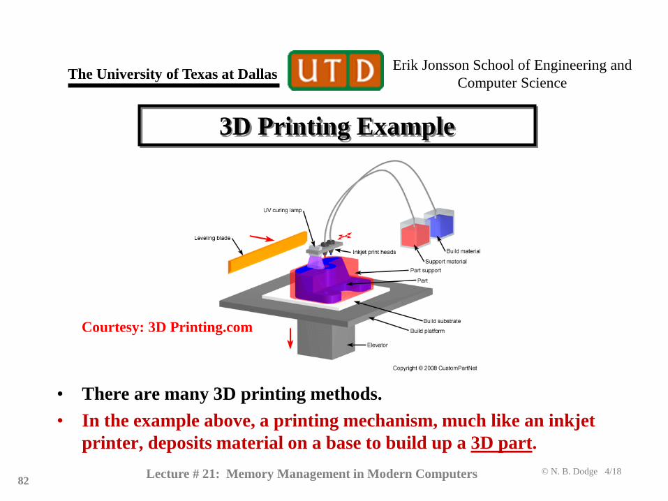
• 3D printers are being used more and more in bioengineering. • Above left: Printed prosthetics for the face and head. • Below left: A 3D printer prints blood vessels and connective tissue matrices. • Above right: Printed “biomatrices” for organ growth.
Lecture # 21: Memory Management in Modern Computers
Erik Jonsson School of Engineering and Computer Science