MCP9843/98243Memory Module Temperature Sensor w/ EEPROM for SPD
Features• Meets JEDEC Specification
- MCP9843 - JC42.4-TSE3000B3 Temperature Sensor
- MCP98243 --> JC42.4-TSE2002B3 Temperature Sensor with 2 Kbit Serial EEPROM for Serial Presence Detect (SPD)
• 2-wire I2C™/SMBus Interface• Available Packages:
- DFN-8, TDFN-8, UDFN-8, TSSOP-8
Temperature Sensor Features• Temperature-to-Digital Converter• Sensor Accuracy (Grade B):
- ±0.2°C/±1°C (typ./max.) → +75°C to +95°C- ±0.5°C/±2°C (typ./max.) → +40°C to +125°C- ±1°C/±3°C (typ./max.) → -20°C to +125°C
• Specified VDD Range: 3.0V to 3.6V• Operating Current: 200 µA (typical)• Operating VDD Range: 2.7V to 5.5V
Serial EEPROM Features (MCP98243)• Specified VDD Range: 1.8V to 5.5V• Operating Current:
- Write → 1.1 mA (typical) for 3.5 ms (typical)- Read → 100 µA (typical)
• Permanent and Reversible Software Write Protect• Software Write Protection for the lower 1 Kbit• Organized as 1 block of 256 x 8-bit (2 Kbit)
Typical Applications• DIMM Modules for Servers, PCs, and Laptops• General Purpose Temperature Datalog
DescriptionMicrochip Technology Inc.’s MCP9843/98243 digitaltemperature sensors convert temperature from -40°Cand +125°C to a digital word. These sensors meetJEDEC Specification JC42.4-TSE3000B3 andJC42.4-TSE2002B3 Memory Module Thermal SensorComponent. It provides an accuracy of ±0.2°C/±1°C(typical/maximum) from +75°C to +95°C. In addition,MCP98243 has an internal 256 Byte EEPROM whichcan be used to store memory module and vendorinformation.
The MCP9843/98243 digital temperature sensorcomes with user-programmable registers that provideflexibility for DIMM temperature-sensing applications.The registers allow user-selectable settings such asShutdown or Low-Power modes and the specificationof temperature Event boundaries. When thetemperature changes beyond the specified Eventboundary limits, the MCP9843/98243 outputs an Alertsignal at the Event pin. The user has the option ofsetting the temperature Event output signal polarity aseither an active-low or active-high comparator outputfor thermostat operation, or as a temperature Eventinterrupt output for microprocessor-based systems.
The MCP98243 EEPROM is designed specifically forDRAM DIMMs (Dual In-line Memory Modules) SerialPresence Detect (SPD). The lower 128 Bytes (address0x00 to 0x7F) can be Permanent Write Protected(PWP) or Software Reversible Write Protected (SWP).This allows DRAM vendor and product information tobe stored and write protected. The upper 128 bytes(address 0x80 to 0xFF) can be used for generalpurpose data storage. These addresses are not writeprotected.
This sensor has an industry standard 2-wire,I2C compatible serial interface, allowing up to eightdevices to be controlled in a single serial bus.
Package TypesDIMM MODULE
MCP9843/98243
8-Pin 2x3 DFN/TDFN/UDFN *
SDAGND
Event
SCL
1
2
3
4
8-Pin TSSOP
A0 VDD
A1A2
8
7
6
5
* Includes Exposed Thermal Pad (EP); see Table 3-1.
Note: This accuracy data from the production system represents the typical accuracy performance of theMCP98242 Memory Module Temperature Sensor. The MCP98242 production methodology is also used forthe MCP9843/98243 to achieve the same typical accuracy performance.
0%
10%
20%
30%
40%
50%
-1.0
-0.8
-0.6
-0.4
-0.2 0.0
0.2
0.4
0.6
0.8
1.0
Temperature Accuracy (°C)
Occ
urre
nces
TA = +85°C1,063,478 units63 Production lots
Statistics:Average = 0.003 °CSt. Dev = 0.13 °C±3 Sigma = ±0.4 °C
MCP98243 VS. MCP98242Feature MCP98243 MCP98242
Event Output in Shutdown Mode Event Output De-asserts Event Output Remains in previous state. If the output asserts before shutdown command, it remains
asserted during shutdown
I2C communication Timeout Range tOUT = 25 ms to 35 ms tOUT = 20 ms to 50 ms
Absolute Maximum Ratings †VDD.................................................................................. 6.0VVoltage at all Input/Output pins ............... GND – 0.3V to 6.0VPin A0 ................................................... GND – 0.3V to 12.5VStorage temperature .....................................-65°C to +150°CAmbient temp. with power applied ................-40°C to +125°CJunction Temperature (TJ) .......................................... +150°CESD protection on all pins (HBM:MM) ................. (4 kV:300V)Latch-Up Current at each pin (25°C) ....................... ±200 mA
†Notice: Stresses above those listed under “Maximumratings” may cause permanent damage to the device. This isa stress rating only and functional operation of the device atthose or any other conditions above those indicated in theoperational listings of this specification is not implied.Exposure to maximum rating conditions for extended periodsmay affect device reliability.
TEMPERATURE SENSOR DC CHARACTERISTICSElectrical Specifications: Unless otherwise indicated, VDD = 3.0V to 3.6V, GND = Ground, and TA = -20°C to +125°C.
Parameters Sym Min Typ Max Unit Conditions
Temperature Sensor Accuracy+75°C < TA ≤ +95°C TACY -1.0 ±0.2 +1.0 °C JC42.4 - TSE2002B3
Grade B Accuracy Specification+40°C < TA ≤ +125°C -2.0 ±0.5 +2.0 °C-20°C < TA ≤ +125°C -3.0 ±1 +3.0 °CTA = -40°C — -1 — °C
Temperature Conversion Time0.25°C/bit tCONV — 65 125 ms 15 s/sec (typical) (See Section 5.2.4)
Power SupplySpecified Voltage Range VDD 3.0 — 3.6 V JC42.4 Specified Voltage RangeOperating Voltage Range VDD 2.7 — 5.5 V Note 1Operating Current IDD_TS — 200 500 µA EEPROM InactiveShutdown Current - MCP9843
MCP98243ISHDN — 1 2 µA EEPROM Inactive, I2C Bus Inactive
— 1 3 µAPower On Reset (POR) VPOR_TS — 2.2 — V Threshold for falling VDD voltagePower Supply Rejection,
TA = +25°C
Δ°C/ΔVDD — ±0.3 — °C/V VDD = 2.7V to 5.5V— ±0.15 — °C VDD = 3.3V+150 mVPP AC
(0 to 1 MHz)Event Output (Open-Drain output, external pull-up or pull-down resistor required), see Section 5.2.3High-level Current (leakage) IOH — — 1 µA VOH = VDD (Active-Low, Pull-up
Resistor)Low-level Voltage VOL — — 0.4 V IOL= 3 mA (Active-Low, Pull-up
Resistor)High-level Voltage VOH — — VDD-0.5 V IOH= 3 mA (Active-High, Pull-down
Resistor)Thermal Response, from +25°C (Air) to +125°C (oil bath)DFN/UDFN/TDFN-8 tRES — 0.7 — s Time to 63% (89°C)TSSOP-8 — 1.4 — sNote 1: Characterized but not production tested. Also, see Section 2.0 “Typical Performance Curves”.
MCP98243 EEPROM DC CHARACTERISTICSElectrical Specifications: Unless otherwise indicated, VDD = 1.8V to 5.5V, GND = Ground, and TA = -20°C to +125°C.
Parameters Sym Min Typ Max Unit ConditionsPower SupplyOperating Voltage Range VDD 1.8 — 5.5 VCurrent, EEPROM write IDD_EE — 1100 2000 µA Sensor in Shutdown Mode (for tWC),
(Note 1)Current, EEPROM read IDD_EE — 100 500 µA Sensor in Shutdown Mode (Note 1)Power On Reset (POR) VPOR_EE — 1.6 — V EEPROMWrite Cycle time (byte/page) tWC — 3 5 msEndurance TA = +25°C — — 1M — cycles Number of Write Cycles, VDD = 5V (Note 2)EEPROM Write Temperature EEWRITE 0 — 85 °CEEPROM Read Temperature EEREAD -40 — 125 °C For minimum read temperature, see Note 2Write Protect VoltageSWP and CWP Voltage VHV 7 — 12 V Applied at A0 pin (Note 3)PWP Voltage — VDD — VNote 1: For VDD ranges of 1.8V to the temperature sensor VPOR_TS, the temperature sensor becomes partially biased and
consumes 80 µA (typical) until the sensor POR resets and acknowledges a shutdown command. See Figure 2-15.2: Characterized but not production tested. For endurance estimates in a specific application, please consult the Total
Endurance™ Model which can be obtained from Microchip’s web site at www.microchip.com.3: The range of voltage applied at A0 pin for Permanent Write Protect is GND to VDD + 1V. See Figure 2-13 and
Section 5.3.3 “Write Protection”.
INPUT/OUTPUT PIN DC CHARACTERISTICS (NOTE 1)Electrical Specifications: Unless otherwise indicated, VDD = 1.8V to 5.5V, GND = Ground andTA = -20°C to +125°C.
Parameters Sym Min Typ Max Units ConditionsSerial Input/Output (SCL, SDA, A0, A1, A2) (Note 2)Input
High-level Voltage VIH 0.7VDD — — VLow-level Voltage VIL — — 0.3VDD VInput Current IIN — — ±5 µA SDA and SCL onlyInput Impedance (A0, A1, A2) ZIN — 1 — MΩ VIN > VIH
Note 1: These specifications apply for the Temperature Sensor and EEPROM.2: For VDD ranges of 1.8V to the temperature sensor VPOR_TS, the temperature sensor becomes partially
biased and consumes 80 µA (typical) until the sensor POR resets and acknowledges a shutdown command. See Figure 2-15.
SENSOR AND EEPROM SERIAL INTERFACE TIMING SPECIFICATIONSElectrical Specifications: Unless otherwise indicated, GND = Ground, TA = -20°C to +125°C, and CL = 80 pF (Note 1, 5).
VDD= 1.8V to 5.5V VDD= 2.2V to 5.5V
Parameters Sym Min Max Min Max Units Conditions
2-Wire I2C InterfaceSerial port frequency fSCL 10 100 10 400 kHz Note 2, 4Low Clock tLOW 4700 — 1300 — ns Note 2High Clock tHIGH 4000 — 600 — ns Note 2Rise time tR — 1000 20 300 nsFall time tF 20 300 20 300 nsData in Setup time tSU:DI 250 — 100 — ns Note 3Data in Hold time tHD:DI 0 — 0 — ns Note 6Data out Hold time tHD:DO 200 900 200 900 ns Note 4Start Condition Setup time tSU:STA 4700 — 600 — nsStart Condition Hold time tHD:STA 4000 — 600 — nsStop Condition Setup time tSU:STO 4000 — 600 — nsBus idle tB:FREE 4700 — 1300 — nsTime out (Sensor Only) tOUT — — 25 35 ms VDD= 3.0V to 3.6VBus Capacitive load Cb — — — 400 pfNote 1: All values referred to VIL MAX and VIH MIN levels.
2: If tLOW > tOUT or tHIGH > tOUT, the temperature sensor I2C interface will time out. A Repeat Start command is required for communication.
3: This device can be used in a Standard-mode I2C-bus system, but the requirement tSU:DAT ≥ 250 ns must be met. This device does not stretch SCL Low time. It outputs the next data bit to the SDA line within tR MAX + tSU:DI MIN = 1000 ns + 250 ns = 1250 ns (according to the Standard-mode I2C-bus specification) before the SCL line is released.
4: As a transmitter, the device provides internal minimum delay time tHD:DAT MIN to bridge the undefined region (min. 300 ns) of the falling edge of SCL tF MAX to avoid unintended generation of Start or Stop conditions.
5: For VDD ranges of 1.8V to the temperature sensor VPOR_TS, the temperature sensor becomes partially biased and consumes 100 µA (typical) until the sensor POR resets and acknowledges a shutdown com-mand.
6: As a receiver, SDA should not be sampled at the falling edge of SCL. SDA can transition tHD:DI 0 ns after SCL toggles Low.
Electrical Specifications: Unless otherwise indicated, VDD = 1.8V to 5.5V for the EEPROM, VDD = 3.0V to 3.6V for the Temperature Sensor, and GND = Ground.
Parameters Sym Min Typ Max Units Conditions
Temperature RangesSpecified Temperature Range TA -20 — +125 °C Note 1Operating Temperature Range TA -40 — +125 °CStorage Temperature Range TA -65 — +150 °CThermal Package ResistancesThermal Resistance, 8L-DFN θJA — 68 — °C/WThermal Resistance, 8L-TDFN θJA — 52.5 — °C/WThermal Resistance, 8L-TSSOP θJA — 139 — °C/WThermal Resistance, 8L-UDFN θJA — 41 — °C/WNote 1: Operation in this range must not cause TJ to exceed Maximum Junction Temperature (+150°C).
Note: Unless otherwise indicated, VDD = 2.7V to 5.5V, GND = Ground, SDA/SCL pulled-up to VDD, andTA = -40°C to +125°C.
FIGURE 2-1: Average Temperature Accuracy.
FIGURE 2-2: Temperature Accuracy Histogram, TA = +95°C.
FIGURE 2-3: Temperature Accuracy Histogram, TA = +75°C.
FIGURE 2-4: Supply Current vs. Temperature.
FIGURE 2-5: Serial Bus Time-Out vs. Temperature.
FIGURE 2-6: Power-on Reset Threshold Voltage vs. Temperature.
Note: The graphs and tables provided following this note are a statistical summary based on a limited number ofsamples and are provided for informational purposes only. The performance characteristics listed hereinare not tested or guaranteed. In some graphs or tables, the data presented may be outside the specifiedoperating range (e.g., outside specified power supply range) and therefore outside the warranted range.
The address pins correspond to the Least Significantbits (LSb) of address bits. The Most Significant bits(MSb) (A6, A5, A4, A3). This is shown in Table 3-2.
The A0 Address pin is a multi-function pin. This inputpin is also used for high voltge input VHV to enable theEEPROM Software Write Protect feature, seeSection 5.3.3 “Write Protection”.
All address pin have an internal pull-down resistors.
3.2 Ground Pin (GND)The GND pin is the system ground pin.
3.3 Serial Data Line (SDA) SDA is a bidirectional input/output pin, used to seriallytransmit data to/from the host controller. This pinrequires a pull-up resistor. (See Section 4.0 “SerialCommunication”).
3.4 Serial Clock Line (SCL)The SCL is a clock input pin. All communication andtiming is relative to the signal on this pin. The clock isgenerated by the host or master controller on the bus.(See Section 4.0 “Serial Communication”).
3.5 Temperature Alert, Open-Drain Output (Event)
The MCP9843/98243 temperature Event output pin isan open-drain output. The device outputs a signalwhen the ambient temperature goes beyond the user-programmed temperature limit. (see Section 5.2.3“Event Output Configuration”).
3.6 Power Pin (VDD)VDD is the power pin. The operating voltage range, asspecified in the DC electrical specification table, isapplied on this pin.
3.7 Exposed Thermal Pad (EP)There is an internal electrical connection between theExposed Thermal Pad (EP) and the GND pin; they canbe connected to the same potential on the Printed Cir-cuit Board (PCB). This provides better thermal conduc-tion from the PCB to the die.
MCP9843/98243Symbol DescriptionDFN, TDFN,
UDFN TSSOP
1 1 A0 Slave Address and EEPROM Software Write Protect high voltage input (VHV)
2 2 A1 Slave Address3 3 A2 Slave Address4 4 GND Ground5 5 SDA Serial Data Line6 6 SCL Serial Clock Line7 7 Event Temperature Alert Output8 8 VDD Power Pin9 — EP Exposed Thermal Pad (EP); can be connected to GND.
4.1 2-Wire Standard Mode I2C™ Protocol-Compatible Interface
The MCP9843/98243 serial clock input (SCL) and thebidirectional serial data line (SDA) form a 2-wirebidirectional Standard mode I2C compatiblecommunication port (refer to the Input/Output Pin DCCharacteristics (Note 1) Table and Sensor AndEEPROM Serial Interface Timing SpecificationsTable).
The following bus protocol has been defined:
TABLE 4-1: MCP9843/98243 SERIAL BUS PROTOCOL DESCRIPTIONS
4.1.1 DATA TRANSFERData transfers are initiated by a Start condition(START), followed by a 7-bit device address and aread/write bit. An Acknowledge (ACK) from the slaveconfirms the reception of each byte. Each access mustbe terminated by a Stop condition (STOP).
Repeated communication is initiated after tB-FREE.
This device does not support sequential register read/write. Each register needs to be addressed using theRegister Pointer.
This device supports the Receive Protocol. Theregister can be specified using the pointer for the initialread. Each repeated read or receive begins with a Startcondition and address byte. The MCP9843/98243retain the previously selected register. Therefore, theyoutput data from the previously-specified register(repeated pointer specification is not necessary).
4.1.2 MASTER/SLAVEThe bus is controlled by a master device (typically amicrocontroller) that controls the bus access andgenerates the Start and Stop conditions. TheMCP9843/98243 is a slave device and does not controlother devices in the bus. Both master and slavedevices can operate as either transmitter or receiver.However, the master device determines which mode isactivated.
4.1.3 START/STOP CONDITION A high-to-low transition of the SDA line (while SCL ishigh) is the Start condition. All data transfers must bepreceded by a Start condition from the master. A low-to-high transition of the SDA line (while SCL is high)signifies a Stop condition.
If a Start or Stop condition is introduced during datatransmission, the MCP9843/98243 releases the bus.All data transfers are ended by a Stop condition fromthe master.
4.1.4 ADDRESS BYTEFollowing the Start condition, the host must transmit an8-bit address byte to the MCP9843/98243. Theaddress for the MCP9843/98243 Temperature Sensoris ‘0011,A2,A1,A0’ in binary, where the A2, A1 andA0 bits are set externally by connecting thecorresponding pins to VDD ‘1’ or GND ‘0’. The 7-bitaddress transmitted in the serial bit stream must matchthe selected address for the MCP9843/98243 torespond with an ACK. Bit 8 in the address byte is aread/write bit. Setting this bit to ‘1’ commands a readoperation, while ‘0’ commands a write operation (seeFigure 4-1).
FIGURE 4-1: Device Addressing.
Term Description
Master The device that controls the serial bus, typically a microcontroller.
Slave The device addressed by the master, such as the MCP9843/98243.
Transmitter Device sending data to the bus.Receiver Device receiving data from the bus.START A unique signal from master to initiate
serial interface with a slave.STOP A unique signal from the master to
terminate serial interface from a slave.Read/Write A read or write to the MCP9843/98243
registers.ACK A receiver Acknowledges (ACK) the
reception of each byte by polling the bus.
NAK A receiver Not-Acknowledges (NAK) or releases the bus to show End-of-Data (EOD).
Busy Communication is not possible because the bus is in use.
Not Busy The bus is in the idle state, both SDA and SCL remain high.
Data Valid SDA must remain stable before SCL becomes high in order for a data bit to be considered valid. During normal data transfers, SDA only changes state while SCL is low.
4.1.5 DATA VALID After the Start condition, each bit of data intransmission needs to be settled for a time specified bytSU-DATA before SCL toggles from low-to-high (see“Sensor And EEPROM Serial Interface TimingSpecifications” on Page 5).
4.1.6 ACKNOWLEDGE (ACK/NAK)Each receiving device, when addressed, is obliged togenerate an ACK bit after the reception of each byte.The master device must generate an extra clock pulsefor ACK to be recognized.
The acknowledging device pulls down the SDA line fortSU-DATA before the low-to-high transition of SCL fromthe master. SDA also needs to remain pulled down fortH-DATA after a high-to-low transition of SCL.
During read, the master must signal an End-of-Data(EOD) to the slave by not generating an ACK bit (NAK)once the last bit has been clocked out of the slave. Inthis case, the slave will leave the data line released toenable the master to generate the Stop condition.
4.1.7 TIME OUT (MCP9843/98243, SENSOR ONLY)
If the SCL stays low or high for time specified by tOUT,the MCP9843/98243 temperature sensor resets theserial interface. This dictates the minimum clock speedas specified in the specification. However, theEEPROM does not reset the serial interface.Therefore, the master can hold the clock indefinitely toprocess data from the EEPROM.
5.0 FUNCTIONAL DESCRIPTIONThe MCP9843/98243 temperature sensors consists ofa band-gap type temperature sensor, a Delta-SigmaAnalog-to-Digital Converter (ΣΔ ADC), user-program-
mable registers and a 2-wire I2C protocol compatibleserial interface. Figure 5-1 shows a block diagram ofthe register structure.
5.1 RegistersThe MCP9843/98243 device has several registers thatare user-accessible. These registers include theCapability register, Configuration register, EventTemperature Upper-Boundary and Lower-BoundaryTrip registers, Critical Temperature Trip register,Temperature register, Manufacturer Identificationregister and Device Identification register.
The Temperature register is read-only, used to accessthe ambient temperature data. The data is loaded inparallel to this register after tCONV. The EventTemperature Upper-Boundary and Lower-BoundaryTrip registers are read/writes. If the ambienttemperature drifts beyond the user-specified limits, theMCP9843/98243 device outputs a signal using theEvent pin (refer to Section 5.2.3 “Event OutputConfiguration”). In addition, the Critical TemperatureTrip register is used to provide an additional criticaltemperature limit.
The Capability register is used to provide bitsdescribing the MCP9843/98243’s capability inmeasurement resolution, measurement range anddevice accuracy. The device Configuration registerprovides access to configure the MCP9843/98243’svarious features. These registers are described infurther detail in the following sections.
The registers are accessed by sending a RegisterPointer to the MCP9843/98243 using the serialinterface. This is an 8-bit write-only pointer. However,the four Least Significant bits are used as pointers andall unused bits (bits 7-4) need to be cleared or set to ‘0’.Register 5-1 describes the pointer or the address ofeach register.
Legend:R = Readable bit W = Writable bit U = Unimplemented bit, read as ‘0’-n = Value at POR ‘1’ = Bit is set ‘0’ = Bit is cleared x = Bit is unknown
bit 7-4 Writable Bits: Write ‘0’’bit 3-0 Pointer Bits:
0000 = Capability register0001 = Configuration register (CONFIG)0010 = Event Temperature Upper-Boundary Trip register (TUPPER)0011 = Event Temperature Lower-Boundary Trip register (TLOWER)0100 = Critical Temperature Trip register (TCRIT)0101 = Temperature register (TA)0110 = Manufacturer ID register0111 = Device ID/Revision register1000 = Resolution register1XXX = Reserved (This device has additional registers that are reserved for test and calibration. If
these registers are accessed, the device may not perform according to the specification.)
5.1.1 CAPABILITY REGISTERThis is a read-only register used to identify thetemperature sensor capability. For example, theMCP9843/98243 device is capable of providingtemperature at 0.25°C resolution, measuringtemperature below and above 0°C, providing ±1°C and±2°C accuracy over the active and monitor temperatureranges (respectively) and providing user-programmable temperature event boundary trip limits.Register 5-2 describes the Capability register. Thesefunctions are described in further detail in the followingsections.
R-1 R-1 R-1 R-0 R-1 R-1 R-1 R-1SHDN Status tOUT Range VHV Resolution Meas Range Accuracy Temp Alarmbit 7 bit 0
Legend:R = Readable bit W = Writable bit U = Unimplemented bit, read as ‘0’-n = Value at POR ‘1’ = Bit is set ‘0’ = Bit is cleared x = Bit is unknown
bit 15-8 Unimplemented: Read as ‘0’
bit 7 Event output status during Shutdown (SHDN Status):0 = Event output remains in previous state. If the output asserts before shutdown command, it
remains asserted during shutdown.1 = Event output de-asserts during shutdown. After shutdown, it takes tCONV to re-assert the Event
output (power-up default)bit 6 I2C Bus time-out (tOUT Range):
0 = Bus time-out range is 10 ms to 60 ms1 = Bus time-out range is 25 ms to 35 ms (power-up default)
bit 5 High Voltage Input0 = Pin A0 does not accept High Voltage1 = Pin A0 accepts High Voltage for the EEPROM Write Protect feature (power-up default)
bit 4-3 Resolution: 00 = 0.5°C01 = 0.25°C (power up default)10 = 0.125°C11 = 0.0625°CThese bits reflect the selected resolution (see Section 5.2.4 “Temperature Resolution”)
bit 2 Temperature Measurement Range (Meas. Range): 0 = TA = 0 (decimal) for temperature below 0°C 1 = The part can measure temperature below 0°C (power-up default)
FIGURE 5-2: Timing Diagram for Reading the Capability Register (See Section 4.0 “Serial Communication”).
bit 1 Accuracy: 0 = Accuracy → ±2°C from +75°C to +95°C (Active Range) and ±3°C from +40°C to +125°C
(Monitor Range)1 = Accuracy → ±1°C from +75°C to +95°C (Active Range) and ±2°C from +40°C to +125°C
(Monitor Range)bit 0 Temperature Alarm:
0 = No defined function (This bit will never be cleared or set to ‘0’)1 = The part has temperature boundary trip limits (TUPPER/TLOWER/TCRIT registers) and a
REGISTER (CONFIG)The MCP9843/98243 device has a 16-bit Configurationregister (CONFIG) that allows the user to set variousfunctions for a robust temperature monitoring system.Bits 10 thru 0 are used to select Event output boundaryhysteresis, device Shutdown or Low-Power mode,temperature boundary and critical temperature lock,temperature Event output enable/disable. In addition,the user can select the Event output condition (outputset for TUPPER and TLOWER temperature boundary orTCRIT only), read Event output status and set Eventoutput polarity and mode (Comparator Output orInterrupt Output mode).
The temperature hysteresis bits 10 and 9 can be usedto prevent output chatter when the ambienttemperature gradually changes beyond the user-specified temperature boundary (see Section 5.2.2“Temperature Hysteresis (THYST)”. The Continuous
Conversion or Shutdown mode is selected using bit 8.In Shutdown mode, the band gap temperature sensorcircuit stops converting temperature and the AmbientTemperature register (TA) holds the previoussuccessfully converted temperature data (seeSection 5.2.1 “Shutdown Mode”). Bits 7 and 6 areused to lock the user-specified boundaries TUPPER,TLOWER and TCRIT to prevent an accidental rewrite.Bits 5 thru 0 are used to configure the temperatureEvent output pin. All functions are described inRegister 5-3 (see Section 5.2.3 “Event OutputConfiguration”).
In shutdown, all power-consuming activities are disabled, though all registers can be written to or read.Event output will de-assert.
This bit cannot be set ‘1’ when either of the lock bits is set (bit 6 and bit 7). However, it can be cleared‘0’ for Continuous Conversion while locked (Refer to Section 5.2.1 “Shutdown Mode”).
bit 7 TCRIT Lock Bit (Crit. Lock):0 = Unlocked. TCRIT register can be written. (power-up default)1 = Locked. TCRIT register can not be written
When enabled, this bit remains set ‘1’ or locked until cleared by internal reset (Section 5.4 “Summaryof Power-on Default”). This bit does not require a double-write.
This bit can be programmed in shutdown mode.bit 6 TUPPER and TLOWER Window Lock Bit (Win. Lock):
0 = Unlocked. TUPPER and TLOWER registers can be written. (power-up default)1 = Locked. TUPPER and TLOWER registers can not be written
When enabled, this bit remains set ‘1’ or locked until cleared by power-on Respell (Section 5.4 “Sum-mary of Power-on Default”). This bit does not require a double-write.
This bit can be programmed in shutdown mode.bit 5 Interrupt Clear (Int. Clear) Bit:
0 = No effect (power-up default)1 = Clear interrupt output. When read this bit returns ‘0’
This bit clears the Interrupt flag which de-asserts Event output. In shutdown mode, the Event output isalways de-asserted. Therefore, setting this bit in shutdown mode clears the interrupt after the devicereturns to normal operation.
bit 4 Event Output Status (Event Stat.) Bit:0 = Event output is not asserted by the device (power-up default)1 = Event output is asserted as a comparator/Interrupt or critical temperature output
In shutdown mode this bit will clear because Event output is always de-asserted in shutdown mode.bit 3 Event Output Control (Event Cnt.) Bit:
This bit can not be altered when either of the lock bits is set (bit 6 and bit 7).
This bit can be programmed in shutdown mode, but Event output will remain de-asserted.bit 2 Event Output Select (Event Sel.) Bit:
0 = Event output for TUPPER, TLOWER and TCRIT (power-up default)1 = TA ≥ TCRIT only. (TUPPER and TLOWER temperature boundaries are disabled.)
When the Alarm Window Lock bit is set, this bit cannot be altered until unlocked (bit 6).
This bit can be programmed in shutdown mode, but Event output will remain de-asserted.bit 1 Event Output Polarity (Event Pol.) Bit:
0 = Active low (power-up default. Pull-up resistor required) See Section 5.2.3 “Event OutputConfiguration”
1 = Active-high (Pull-down resistor required) See Section 5.2.3 “Event Output Configuration”This bit cannot be altered when either of the lock bits is set (bit 6 and bit 7).
This bit can be programmed in shutdown mode, but Event output will remain de-asserted.bit 0 Event Output Mode (Event Mod.) Bit:
The MCP9843/98243 device has a 16-bit read/writeEvent output Temperature Upper-Boundary Tripregister (TUPPER), a 16-bit Lower-Boundary Tripregister (TLOWER) and a 16-bit Critical Boundary Tripregister (TCRIT) that contains 11-bit data in two’scomplement format (0.25°C). This data represents themaximum and minimum temperature boundary ortemperature window that can be used to monitorambient temperature. If this feature is enabled(Section 5.1.2 “Sensor Configuration Register(CONFIG)”) and the ambient temperature exceeds thespecified boundary or window, the MCP9843/98243asserts an Event output. (Refer to Section 5.2.3“Event Output Configuration”).
REGISTER 5-4: UPPER/LOWER/CRITICAL TEMPERATURE LIMIT REGISTER (TUPPER/TLOWER/
REGISTER (TA)The MCP9843/98243 device uses a band gaptemperature sensor circuit to output analog voltageproportional to absolute temperature. An internal ΔΣADC is used to convert the analog voltage to a digitalword. The converter resolution is set to 0.25°C + sign(11-bit data). The digital word is loaded to a 16-bit read-only Ambient Temperature register (TA) that contains11-bit temperature data in two’s complement format.
The TA register bits (bits 12 thru 0) are double-buffered.Therefore, the user can access the register while, in thebackground, the MCP9843/98243 performs an analog-to-digital conversion. The temperature data from the ΔΣADC is loaded in parallel to the TA register at tCONVrefresh rate.
In addition, the TA register uses three bits (bits 15, 14and 13) to reflect the Event pin state. This allows theuser to identify the cause of the Event output trigger(see Section 5.2.3 “Event Output Configuration”);bit 15 is set to ‘1’ if TA is greater than or equal to TCRIT,bit 14 is set to ‘1’ if TA is greater than TUPPER and bit 13is set to ‘1’ if TA is less than TLOWER.
The TA register bit assignment and boundaryconditions are described in Register 5-5.
R-0 R-0 R-0 R-0 R-0 R-0 R-0 R-0TA vs. TCRIT TA vs. TUPPER TA vs. TLOWER SIGN 27 °C 26 °C 25 °C 24 °Cbit 15 bit 8
R-0 R-0 R-0 R-0 R-0 R-0 R-0 R-023 °C 22 °C 21 °C 20 °C 2-1 °C 2-2 °C 2-3 °C 2-4 °C
bit 7 bit 0
Legend:R = Readable bit W = Writable bit U = Unimplemented bit, read as ‘0’-n = Value at POR ‘1’ = Bit is set ‘0’ = Bit is cleared x = Bit is unknown
bit 15 TA vs. TCRIT (1) Bit:
0 = TA < TCRIT1 = TA ≥ TCRIT
bit 14 TA vs. TUPPER (1) Bit:0 = TA ≤ TUPPER1 = TA > TUPPER
bit 13 TA vs. TLOWER (1) Bit:0 = TA ≥ TLOWER1 = TA < TLOWER
bit 12 SIGN Bit:0 = TA ≥ 0°C 1 = TA < 0°C
bit 11-0 Ambient Temperature (TA) Bits: (Note 2)12-bit Ambient Temperature data in two’s complement format.
Note 1: Bits 15, 14 and 13 are not affected by the status of the Event output configuration (bits 5 to 0 of CONFIG)(Register 5-3).
2: Bits 2, 1, and 0 may remain clear '0' depending on the status of the resolution register (Register 5-9).The Power-up default is 0.25°C/bit, bits 1 and 0 remain clear '0'.
5.1.4.1 TA bits to Temperature ConversionTo convert the TA bits to decimal temperature, theupper three boundary bits (bits 15, 14 and 13) must bemasked out. Then determine the sign bit (bit 12) tocheck positive or negative temperature, shift the bitsaccordingly and combine the upper and lower bytes ofthe 16-bit register. The upper byte contains data fortemperatures greater than 32°C while the lower bytecontains data for temperature less than 32°C, includingfractional data. When combinding the upper and lowerbytes, the upper byte must be Right-shifted by 4bits (ormultiply by 24) and the lower byte must be Left-shiftedby 4 bits (or multiply by 2-4). Adding the results of theshifted values provides the temperature data in decimalformat, see Equation 5-1.
The temperature bits are in two’s compliment format,therefore, postive temperature data and negative tem-perature data are computed differently. Equation 5-1shows the temperature computation. The exampleinstruction code outlined in Figure 5-6 shows thecommunication flow, also see Figure 5-7 for timingdiagram.
EQUATION 5-1: BYTES TO TEMPERATURE CONVERSION
FIGURE 5-6: Example Instruction Code.
Where:
TA = Ambient Temperature (°C)UpperByte = TA bit 15 to bit 8LowerByte = TA bit 7 to bit 0
//also, make sure bit 0 is cleared ‘0’i2c_write(0x05); // Write TA Register Addressi2c_start(); //Repeat STARTi2c_write(AddressByte | 0x01); // READ Command
//also, make sure bit 0 is Set ‘1’UpperByte = i2c_read(ACK); // READ 8 bits
5.1.5 MANUFACTURER ID REGISTER This register is used to identify the manufacturer of thedevice in order to perform manufacturer specificoperation. The Manufacturer ID for the MCP9843/98243 is 0x0054 (hexadecimal).
FIGURE 5-8: Timing Diagram for Reading the Manufacturer ID Register (See Section 4.0 “Serial Communication”).
REGISTER 5-6: MANUFACTURER ID REGISTER (READ-ONLY) → ADDRESS ‘0000 0110’b
R-0 R-0 R-0 R-0 R-0 R-0 R-0 R-0Manufacturer ID
bit 15 bit 8
R-0 R-1 R-0 R-1 R-0 R-1 R-0 R-0Manufacturer ID
bit 7 bit 0
Legend:R = Readable bit W = Writable bit U = Unimplemented bit, read as ‘0’-n = Value at POR ‘1’ = Bit is set ‘0’ = Bit is cleared x = Bit is unknown
bit 15-0 Device Manufacturer Identification Number.
SDAACK
0 0 1 1 A
Manuf. ID Pointer
0 0 0 0ACKS 2
A1
A0
1 2 3 4 5 6 7 8 1 2 3 4 5 6 7 8
SCL
0
Address Byte
ACK
0 0 1 1 A
MSB Data
ACK
NAK
S P2A1
A0
1 2 3 4 5 6 7 8 1 2 3 4 5 6 7 8 1 2 3 4 5 6 7 8
Address Byte LSB Data
R
MCP9843/98243 MCP9843/98243
MCP9843/98243 Master Master
W
SDA
SCL
1 1 0
0 0 0 0 0 0 0 0 0 1 0 1 0 1 0 0
Note: It is not necessary toselect the registerpointer if it was set fromthe previous read/write.
REGISTERThe upper byte of this register is used to specify thedevice identification and the lower byte is used tospecify device revision. The device ID for theMCP98243 is 0x21 (hex) and the MCP9843 is 0x00(hex).
The revision (Lower Byte) begins with 0x00 (hex) forthe first release, with the number being incremented asrevised versions are released. The revision for bothMCP9843 and MCP98243 is 0x01.
REGISTER 5-7: MCP98243 DEVICE ID AND DEVICE REVISION (READ-ONLY) → ADDRESS ‘0000 0111’b
R-0 R-0 R-1 R-0 R-0 R-0 R-0 R-1Device ID
bit 15 bit 8
R-0 R-0 R-0 R-0 R-0 R-0 R-0 R-1Device Revision
bit 7 bit 0
Legend:R = Readable bit W = Writable bit U = Unimplemented bit, read as ‘0’-n = Value at POR ‘1’ = Bit is set ‘0’ = Bit is cleared x = Bit is unknown
bit 15-8 Device ID: Bit 15 to bit 8 are used for device IDbit 7-0 Device Revision: Bit 7 to bit 0 are used for device revision
REGISTER 5-8: MCP9843 DEVICE ID AND DEVICE REVISION (READ-ONLY) → ADDRESS ‘0000 0111’b
R-0 R-0 R-0 R-0 R-0 R-0 R-0 R-0Device ID
bit 15 bit 8
R-0 R-0 R-0 R-0 R-0 R-0 R-0 R-1Device Revision
bit 7 bit 0
Legend:R = Readable bit W = Writable bit U = Unimplemented bit, read as ‘0’-n = Value at POR ‘1’ = Bit is set ‘0’ = Bit is cleared x = Bit is unknown bit 15-8 Device ID: Bit 15 to bit 8 are used for device IDbit 7-0 Device Revision: Bit 7 to bit 0 are used for device revision
5.1.7 RESOLUTION REGISTERThis register allows the user to change the sensorresolution (see Section 5.2.4 “TemperatureResolution”). The POR default resolution is 0.25°C.The selected resolution is also reflected in theCapability register (see Register 5-2).
FIGURE 5-9: Timing Diagram for Changing TA Resolution to 0.0625°C <0000 0011>b (See Section 4.0 “Serial Communication”).
5.2.1 SHUTDOWN MODEShutdown mode disables all power-consumingactivities (including temperature sampling operations)while leaving the serial interface active. This mode isselected by setting bit 8 of CONFIG to ‘1’. In this mode,the device consumes ISHDN. It remains in this modeuntil bit 8 is cleared ‘0’ to enable ContinuousConversion mode, or until power is recycled.
The Shutdown bit (bit 8) cannot be set to ‘1’ while bits6 and 7 of CONFIG (Lock bits) are set to ‘1’. However,it can be cleared ‘0’ or returned to ContinuousConversion while locked.
In Shutdown mode, all registers can be read or written.However, the serial bus activity increases the shutdowncurrent.
If the device is shutdown while the Event pin isasserted, then the Event output will be de-assertedduring shutdown. It will remain de-asserted until thedevice is enabled for normal operation. Once thedevice is enabled it takes tCONV before the devicere-asserts the Event output.
5.2.2 TEMPERATURE HYSTERESIS (THYST)
A hysteresis of 0°C, 1.5°C, 3°C or 6°C can be selectedfor the TUPPER, TLOWER and TCRIT temperateboundaries using bits 10 and 9 of CONFIG. Thehysteresis applies for decreasing temperature only (hotto cold), or as temperature drifts below the specifiedlimit.
The hysteresis bits can not be changed if either of thelock bits, bits 6 and 7 of CONFIG, are set to ‘1’.
The TUPPER, TLOWER and TCRIT boundary conditionsare described graphically in Figure 5-2.
5.2.3 EVENT OUTPUT CONFIGURATIONThe Event output can be enabled using bit 3 ofCONFIG (Event output control bit) and can beconfigured as either a comparator output or as InterruptOutput mode using bit 0 of CONFIG (Event mode). Thepolarity can also be specified as an active-high oractive-low using bit 1 of CONFIG (Event polarity).When active-high output is selected, a pull-downresistor is requried on the Event pin. When active-lowoutput is selected, a pull-up resistor is required on theEvent pin, see Figure 5-10 and Figure 5-11 forgraphical circuit description. These configurations aredesigned to serve processors with Low-to-High orHigh-to-Low edge triggered inputs. With theseconfigurations, when the Event output De-asserts,power will not be dissipated across the pull-up orpull-down resistors.
When the ambient temperature increases above thecritical temperature limit, the Event output is forced to acomparator output (regardless of bit 0 of CONFIG).When the temperature drifts below the criticaltemperature limit minus hysteresis, the Event outputautomatically returns to the state specified by bit 0 ofCONFIG.
FIGURE 5-11: Active-Low Event Output Configuration.The status of the Event output can be read using bit 4of CONFIG (Event status). This bit can not be set to ‘1’in shutdown mode.
Bit 7 and 6 of the CONFIG register can be used to lockthe TUPPER, TLOWER and TCRIT registers. The bitsprevent false triggers at the Event output due to anaccidental rewrite to these registers.
The Event output can also be used as a criticaltemperature output using bit 2 of CONFIG (criticaloutput only). When this feature is selected, the Eventoutput becomes a comparator output. In this mode, theinterrupt output configuration (bit 0 of CONFIG) isignored.
5.2.3.1 Comparator ModeComparator mode is selected using bit 0 of CONFIG. Inthis mode, the Event output is asserted as active-highor active-low using bit 1 of CONFIG. Figure 5-12 showsthe conditions that toggle the Event output.
If the device enters Shutdown mode with assertedEvent output, the output will de-assert. It will remain de-asserted until the device enters Continuous Conver-sion mode and after the first temperature conversion iscompleted, tCONV. After the initial temperature conver-sion, TA must satisfy the TUPPER or TLOWER boundaryconditions in order for Event output to be asserted.
Comparator mode is useful for thermostat-typeapplications, such as turning on a cooling fan ortriggering a system shutdown when the temperatureexceeds a safe operating range.
5.2.3.2 Interrupt ModeIn the Interrupt mode, the Event output is asserted asactive-high or active-low (depending on the polarityconfiguration) when TA drifts above or below TUPPERand TLOWER limits. The output is deasserted by settingbit 5 (Interrupt Clear) of CONFIG. If the device entersShutdown mode with asserted Event output, the outputwill de-assert. It will remain de-asserted until the deviceenters Continuous Conversion mode and after the firsttemperature conversion is completed, tCONV. If the inter-rupt clear bit (Bit 5) is never set, then the Event output willre-assert after the first temperature conversion.
In addition, if TA >= TCRIT the Event output is forced asComparator mode and asserts until TA < TCRIT - THYST.While the Event output is asserted, user must send ClearInterrupt command (bit 5 of CONFIG) for Event output tode-assert, when temperature drops below the criticallimit, TA < TCRIT - THYST. Otherwise, Event outputremains asserted (see Figure 5-12 for graphical descrip-tion). Switching from Interrupt mode to Comparator modealso de-asserts Event output.
This mode is designed for interrupt driven microcontrollerbased systems. The microcontroller receiving theinterrupt will have to acknowledge the interrupt by settingbit 5 of CONFIG register from the MCP9843/98243.
5.2.4 TEMPERATURE RESOLUTIONThe MCP9843/98243 device is capable of providing atemperature data with 0.5°C to 0.0625°C resolution.The Resolution can selected using the Resolutionregister (Register 5-9) which is located in address‘00001000’b. This address location is not specified inJEDEC Standard JC42.4. However, it providesadditional flexibility while being functionally compatiblewith JC42.4 and provide a 0.25°C resolution at 125 ms(max.). The selected resolution can be read by userusing bit 4 and bit 3 of the Capability register(Register 5-2). A 0.25°C resolution is set as PORdefault by factory.
Note Output Boundary ConditionsComparator Interrupt Critical TA Bits
Output State (Active Low/High) 15 14 13
1 TA ≥ TLOWER High/Low Low/High High/Low 0 0 02 TA < TLOWER - THYST Low/High Low/High High/Low 0 0 13 TA > TUPPER Low/High Low/High High/Low 0 1 04 TA ≤ TUPPER - THYST High/Low Low/High High/Low 0 0 05 TA ≥ TCRIT Low/High Low/High Low/High 1 1 06 When TA ≥ TCRIT the Event output is forced to Comparator Mode and bits 0 of CONFIG (Event
output mode) is ignored until TA < TCRIT - THYST. In the Interrupt Mode, if Interrupt is not cleared (bits 5 of CONFIG) as shown in the diagram at Note 6, then Event will remain asserted at Note 7 until Interrupt is cleared by the controller.
5.3.1 BYTE WRITETo write a byte in the MCP98243 EEPROM, the masterhas to specify the memory location or address. Oncethe address byte is transmitted correctly followed by aword address, the word address is stored in theEEPROM address pointer. The following byte is datato be stored in the specified memory location. Figure 5-13 shows the timing diagram.
FIGURE 5-13: Timing Diagram for Byte Write (See Section 4.0 “Serial Communication”).
5.3.2 PAGE WRITE The write Address Byte, word address and the first databyte are transmitted to the MCP98243 in the same wayas in a byte write. Instead of generating a Stopcondition, the master transmits up to 15 additional databytes to the MCP98243, which are temporarily storedin the on-chip page buffer and will be written into thememory after the master has transmitted a Stopcondition. Upon receipt of each word, the four lowerorder address pointer bits are internally incremented byone. The higher order four bits of the word addressremain constant. If the master should transmit morethan 16 bytes prior to generating the Stop condition, theaddress counter will roll over and the previouslyreceived data will be overwritten. As with the byte writeoperation, once the Stop condition is received, aninternal write cycle will begin (Figure 5-14).
FIGURE 5-14: Timing Diagram for Page Write (See Section 4.0 “Serial Communication”).
Note: Page write operations are limited to writingbytes within a single physical page,regardless of the number of bytes actuallybeing written. Physical page boundariesstart at addresses that are integermultiples of the page buffer size (or ‘pagesize’) and end at addresses that areinteger multiples of [page size - 1]. If aPage Write command attempts to writeacross a physical page boundary, theresult is that the data wraps around to thebeginning of the current page (overwritingdata previously stored there), instead ofbeing written to the next page, as might beexpected. It is therefore necessary for theapplication software to prevent page writeoperations that would attempt to cross apage boundary.
5.3.3 WRITE PROTECTIONThe MCP98243 has a Software Write-Protect (SWP)feature that allows the lower half array (addresses00h - 7Fh) to be write-protected or permanently write-protected (PWP). The write protected area can becleared by sending Clear Write Protect (CWP)command. However, once the PWP is executed theprotected memory can not be cleared. The device willnot respond to the CWP command.
To access write protection, the device address code ofthe Address Byte is set to ‘0110’ instead of ‘1010’. The‘1010’ Address code is used to access the memoryarea and the ‘0110’ address code is used to access thewrite protection. Once the device is write protected itwill not acknowledge certain commands. Table 5-3shows the corresponding Address Bytes for the writeprotect feature.
Note 1: The Address Pins are ‘X’ or don’t cares. However, the slave address bits need to match the address pins. For VHV voltage levels, refer to Figure 2-13.
TABLE 5-4: DEVICE RESPONSE WHEN WRITING DATA OR ACCESSING SWP/CWP/PWP (NOTE 1)
Status Command ACK Address ACK Data Byte ACK Write Cycle
NotProtected
SWP/CWP/PWP ACK X ACK X ACK YesPage/byte write ACK Address ACK Data ACK Yes
Protectedwith SWP
SWP NoACK X NoACK X NoACK NoCWP ACK X ACK X ACK YesPWP ACK X ACK X ACK Yes
5.3.3.1 Software Write Protect (SWP)The SWP feature is invoked by writing to the write-protect register. This is done by sending an AddressByte similar to a normal Write command. Figure 5-17shows the timing diagram. SWP can be cleared usingthe CWP command. See Section 5.3.3.2 “Clear WriteProtect (CWP)”
The Slave Address bits need to correspond to theaddress pin logic configuration. For SWP, a highvoltage VHV needs to be applied to the A0 pin and thecorresponding slave address needs to be set to ‘1’, asshown in Table 5-3. Both A2 and A1 pins are groundedand the corresponding slave address bits are set to ‘0’.
The device response in this mode is shown in Table 5-4 and Table 5-5.
FIGURE 5-15: Timing Diagram for Setting Software Write Protect (See Section 4.0 “Serial Communication”).
5.3.3.2 Clear Write Protect (CWP)The CWP feature is invoked by writing to the clearwrite-protect register. This is done by sending anAddress Byte similar to a normal Write command.Figure 5-17 shows the timing diagram. CWP clearsSWP only. PWP can not be cleared using thiscommand.
The Slave Address bits need to correspond to theaddress pin logic configuration. For CWP, a highvoltage VHV needs to be applied to the A0 pin and thecorresponding slave address needs to be set to ‘1’.The A1 pin is set to VDD and the corresponding slaveaddress bit is set to ‘1’. And A2 pins is set to groundand the corresponding slave address bits are set to ‘0’.Table 5-3 shows the bit configuration. The deviceresponse in this mode is shown in Table 5-4 andTable 5-5.
FIGURE 5-16: Timing Diagram for Setting Clear Write Protect (See Section 4.0 “Serial Communication”).
SDAACK
0 1 1 0ACK
S
1 2 3 4 5 6 7 8 1 2 3 4 5 6 7 8
SCL
Address Byte
W
MCP98243 MCP98243
ACK
P
1 2 3 4 5 6 7 8
DataWord Address
MCP98243
X X X X X X X X X X X X X X X X0 0 1
Note: Apply VHV at A0 pin and connect GND to A1 and A2 pins to initiate SWP cycle.
SDAACK
0 1 1 0ACK
S
1 2 3 4 5 6 7 8 1 2 3 4 5 6 7 8
SCL
Address Byte
W
MCP98243 MCP98243
ACK
P
1 2 3 4 5 6 7 8
DataWord Address
MCP98243
X X X X X X X X X X X X X X X X0 1 1
Note: Apply VHV at A0 pin, apply VDD at A1 pin, connect A2 pin to GND to initiate CWP cycle.
5.3.3.3 PWP (Permanent Write Protect)Once the PWP register is written, the lower half of thememory will be permanent protected and the devicewill not acknowledge any command. The protectedarea of the memory can not be cleared, reversed, or re-written. If a write is attempted to the protected area, thedevice will acknowledge the address byte and wordaddress but not the data byte. (See Table 5-4 andTable 5-5).
Unlike SWP and CWP, a VHV is not applied on the A0pin to execute PWP. The state of A2, A1, and A0 is userselectable. However, the address pin states need tomatch the slave address bits, as shown in Table 5-3.
FIGURE 5-17: Timing Diagram for Setting Permanent Write Protect (See Section 4.0 “Serial Communication”).
Note: Once the Permanent Write-Protect isexecuted, it cannot be reversed, even if thedevice power is cycled. See Figure 2-13for VHV voltage levels.
SDAACK
0 1 1 0 A ACK
S 2A1
A0
1 2 3 4 5 6 7 8 1 2 3 4 5 6 7 8
SCL
Address Byte
W
MCP98243 MCP98243
ACK
P
1 2 3 4 5 6 7 8
DataWord Address
MCP98243
X X X X X X X X X X X X X X X X
Note: Unlike SWP and CWP, VHV must be within the range of GND to VDD + 1V to execute PWP.See Figure 2-13 and Section 5.3.3 “Write Protection”.
5.3.4 READ OPERATIONRead operations are initiated in the same way as writeoperations, with the exception that the R/W bit of theslave address is set to ‘1’. There are three basic typesof read operations: current address read, random readand sequential read.
5.3.4.1 Current Address ReadThe MCP98243 contains an address counter thatmaintains the address of the last word accessed,internally incremented by ‘1’. Therefore, if the previousaccess (either a read or write operation) was toaddress n, the next current address read operationwould access data from address n+1. Upon receipt ofthe slave address with R/W bit set to ‘1’, the MCP98243issues an acknowledge and transmits the 8-bit data
word. The master will not acknowledge (NAK) thetransfer but does generate a Stop condition and theMCP98243 discontinues transmission (Figure 5-18).
FIGURE 5-18: Reading Current Word Address (See Section 4.0 “Serial Communication”).
TABLE 5-5: DEVICE RESPONSE WHEN READING SWP/CWP/PWP (NOTE)Status Command ACK Address ACK Data Byte ACK
Not Protected SWP/CWP/PWP ACK X NoACK X NoACK
Protected with SWPSWP NoACK X NoACK X NoACKCWP ACK X NoACK X NoACKPWP ACK X NoACK X NoACK
Permanently Protected SWP/CWP/PWP NoACK X NoACK X NoACKNote: X is defined as ‘don’t care’.
1 0 1 0 A ACK
NAK
S P2A1
A0
1 2 3 4 5 6 7 8 1 2 3 4 5 6 7 8
Address Byte Current Word Address
R
MCP98243 Master
SDA
SCL
0 0 0 0 0 0 0 0
Note: In this example, the current word address is thepreviously accessed address location n plus 1.
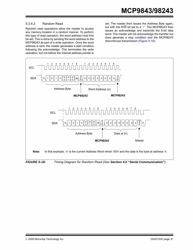
5.3.4.2 Random ReadRandom read operations allow the master to accessany memory location in a random manner. To performthis type of read operation, the word address must firstbe set. This is done by sending the word address to theMCP98243 as part of a write operation. Once the wordaddress is sent, the master generates a start conditionfollowing the acknowledge. This terminates the writeoperation, but not before the internal address pointer is
set. The master then issues the Address Byte again,but with the R/W bit set to a ‘1’. The MCP98243 thenissues an acknowledge and transmits the 8-bit dataword. The master will not acknowledge the transfer butdoes generate a stop condition and the MCP98243discontinues transmission (Figure 5-19).
FIGURE 5-19: Timing Diagram for Random Read (See Section 4.0 “Serial Communication”).
SDAACK
1 0 1 0 A
Word Address (n)
0 0 0 0ACK
S 2A1
A0
1 2 3 4 5 6 7 8 1 2 3 4 5 6 7 8
SCL
0
Address Byte
MCP98243 MCP98243
W 0 0 0
1 0 1 0 A ACK
NAK
S P2A1
A0
1 2 3 4 5 6 7 8 1 2 3 4 5 6 7 8
Address Byte Data at (n)
R
MCP98243 Master
SDA
SCL
X X X X X X X X
Note: In this example, ‘n’ is the current Address Word which ‘00’h and the data is the byte at address ‘n’.
5.3.4.3 Sequential ReadSequential reads are initiated in the same way as arandom read, with the exception that after theMCP98243 transmits the first data byte, the masterissues an acknowledge, as opposed to a stop conditionin a random read. This directs the MCP98243 totransmit the next sequentially addressed 8-bit word(Figure 5-20).
To provide sequential reads, the MCP98243 containsan internal address pointer, which is incremented byone at the completion of each operation. This addresspointer allows the entire memory contents to be seriallyread during one operation.
FIGURE 5-20: Timing Diagram for Sequential Read (See Section 4.0 “Serial Communication”).
5.3.5 STANDBY MODEThe design will incorporate a low power standby mode(ISHDN). Standby mode will be entered after a normaltermination of any operation and after all internalfunctions are complete. This would include any errorconditions occurring, such as improper number of clockcycles or improper instruction byte as definedpreviously.
SDAACK
1 0 1 0 A X X X XACKS 2
A1
A0
1 2 3 4 5 6 7 8 1 2 3 4 5 6 7 8
SCL
X
Address Byte
R
MCP98243 MCP98243
Data at (n+1)
ACK
1 2 3 4 5 6 7 8 1 2 3 4 5 6 7 8
Data at (n+2)
Data (n)1
MCP98243 MCP98243
X X X
X X X X X X X X X X X X X X X X
Data at (n+m)(1)
X X X X X XACK
Note 1: ‘n’ is the initial address location and ‘m’ is the final address location (‘n+m’ < 256)
5.4 Summary of Power-on DefaultThe MCP9843/98243 has an internal Power-on Reset(POR) circuit. If the power supply voltage VDD glitchesdown to the VPOR_TS and VPOR_EE thresholds, thedevice resets the registers to the power-on defaultsettings.
Table 5-6 shows the power-on default summary for thetemperature sensor. The EEPROM resets the addresspointer to 0x00 hex.
TABLE 5-6: MCP9843/98243 TEMPERATURE SENSOR POWER-ON RESET DEFAULTSRegisters
Default RegisterData (Hexadecimal)
Power-up Default Register DescriptionAddress
(Hexadecimal) Register Name
0x00 Capability 0x00EF Event output de-asserts in shutdownI2C time out 25 ms to 35 ms.
Accepts VHV at A0 Pin0.25°C Measurement ResolutionMeasures temperature below 0°C±1°C accuracy over active range
Temperature event output 0x01 CONFIG 0x0000 Comparator mode
Active-Low outputEvent and critical output
Output disabledEvent not assertedInterrupt cleared
Event limits unlockedCritical limit unlocked
Continuous conversion0°C Hysteresis
0x02 TUPPER 0x0000 0°C0x03 TLOWER 0x0000 0°C0x04 TCRIT 0x0000 0°C0x05 TA 0x0000 0°C0x06 Manufacturer ID 0x0054 0x0054 (hex)0x07 Device ID/ Device Revision for
6.1 Layout ConsiderationsThe MCP9843/98243 device does not require anyadditional components besides the master controller inorder to measure temperature. However, it is recom-mended that a decoupling capacitor of 0.1 µF to 1 µFbe used between the VDD and GND pins. A high-frequency ceramic capacitor is recommended. It isnecessary for the capacitor to be located as close aspossible to the power and ground pins of the device inorder to provide effective noise protection.
In addition, good PCB layout is key for better thermalconduction from the PCB temperature to the sensordie. For good temperature sensitivity, add a groundlayer under the device pins as shown in Figure 6-1.
6.2 Thermal ConsiderationsA potential for self-heating errors can exist if theMCP9843/98243 SDA, SCLK and Event lines areheavily loaded with pull-ups (high current). Typically,the self-heating error is negligible because of therelatively small current consumption of the MCP9843/98243. A temperature accuracy error of approximately0.5°C could result from self-heating if thecommunication pins sink/source the maximum currentspecified.
For example, if the Event output is loaded to maximumIOL, Equation 6-1 can be used to determine the effectof self-heating.
EQUATION 6-1: EFFECT OF SELF-HEATING
At room temperature (TA = +25°C) with maximumIDD = 500 µA and VDD = 3.6V, the self-heating due topower dissipation TΔ is 0.2°C for the DFN-8 packageand 0.5°C for the TSSOP-8 package.
Legend: XX...X Customer-specific informationY Year code (last digit of calendar year)YY Year code (last 2 digits of calendar year)WW Week code (week of January 1 is week ‘01’)NNN Alphanumeric traceability code Pb-free JEDEC designator for Matte Tin (Sn)* This package is Pb-free. The Pb-free JEDEC designator ( )
can be found on the outer packaging for this package.
Note: In the event the full Microchip part number cannot be marked on one line, it willbe carried over to the next line, thus limiting the number of availablecharacters for customer-specific information.
Note the following details of the code protection feature on Microchip devices:• Microchip products meet the specification contained in their particular Microchip Data Sheet.
• Microchip believes that its family of products is one of the most secure families of its kind on the market today, when used in the intended manner and under normal conditions.
• There are dishonest and possibly illegal methods used to breach the code protection feature. All of these methods, to our knowledge, require using the Microchip products in a manner outside the operating specifications contained in Microchip’s Data Sheets. Most likely, the person doing so is engaged in theft of intellectual property.
• Microchip is willing to work with the customer who is concerned about the integrity of their code.
• Neither Microchip nor any other semiconductor manufacturer can guarantee the security of their code. Code protection does not mean that we are guaranteeing the product as “unbreakable.”
Code protection is constantly evolving. We at Microchip are committed to continuously improving the code protection features of ourproducts. Attempts to break Microchip’s code protection feature may be a violation of the Digital Millennium Copyright Act. If such actsallow unauthorized access to your software or other copyrighted work, you may have a right to sue for relief under that Act.
Information contained in this publication regarding deviceapplications and the like is provided only for your convenienceand may be superseded by updates. It is your responsibility toensure that your application meets with your specifications.MICROCHIP MAKES NO REPRESENTATIONS ORWARRANTIES OF ANY KIND WHETHER EXPRESS ORIMPLIED, WRITTEN OR ORAL, STATUTORY OROTHERWISE, RELATED TO THE INFORMATION,INCLUDING BUT NOT LIMITED TO ITS CONDITION,QUALITY, PERFORMANCE, MERCHANTABILITY ORFITNESS FOR PURPOSE. Microchip disclaims all liabilityarising from this information and its use. Use of Microchipdevices in life support and/or safety applications is entirely atthe buyer’s risk, and the buyer agrees to defend, indemnify andhold harmless Microchip from any and all damages, claims,suits, or expenses resulting from such use. No licenses areconveyed, implicitly or otherwise, under any Microchipintellectual property rights.
The Microchip name and logo, the Microchip logo, dsPIC, KEELOQ, KEELOQ logo, MPLAB, PIC, PICmicro, PICSTART, rfPIC and UNI/O are registered trademarks of Microchip Technology Incorporated in the U.S.A. and other countries.
FilterLab, Hampshire, HI-TECH C, Linear Active Thermistor, MXDEV, MXLAB, SEEVAL and The Embedded Control Solutions Company are registered trademarks of Microchip Technology Incorporated in the U.S.A.
Analog-for-the-Digital Age, Application Maestro, CodeGuard, dsPICDEM, dsPICDEM.net, dsPICworks, dsSPEAK, ECAN, ECONOMONITOR, FanSense, HI-TIDE, In-Circuit Serial Programming, ICSP, Mindi, MiWi, MPASM, MPLAB Certified logo, MPLIB, MPLINK, mTouch, Octopus, Omniscient Code Generation, PICC, PICC-18, PICDEM, PICDEM.net, PICkit, PICtail, PIC32 logo, REAL ICE, rfLAB, Select Mode, Total Endurance, TSHARC, UniWinDriver, WiperLock and ZENA are trademarks of Microchip Technology Incorporated in the U.S.A. and other countries.
SQTP is a service mark of Microchip Technology Incorporated in the U.S.A.
All other trademarks mentioned herein are property of their respective companies.
Microchip received ISO/TS-16949:2002 certification for its worldwide headquarters, design and wafer fabrication facilities in Chandler and Tempe, Arizona; Gresham, Oregon and design centers in California and India. The Company’s quality system processes and procedures are for its PIC® MCUs and dsPIC® DSCs, KEELOQ® code hopping devices, Serial EEPROMs, microperipherals, nonvolatile memory and analog products. In addition, Microchip’s quality system for the design and manufacture of development systems is ISO 9001:2000 certified.