15
MEMS in GaN Peter Benkart, Ulrich Heinle, Mike Kunze, Ingo Daumiller and Ertugrul Sönmez

MEMS in GaNPeter Benkart, Ulrich Heinle, Mike Kunze,
Ingo Daumiller and Ertugrul Sönmez

A further use, dissemination or publication of this material is only allowed after pre-approval and along with theauthor's permission. All rights at MicroGaN GmbH.
GaN-MEMS Overview
GaN-MEMS sensor GaN-MEMS actuator
Application examples: - sensing elements in pressure sensors - proximity sensor with sub-micron resolution
Advantages of GaN-MEMS - high measurement signal - functionality shown until 300°C (more can be expected) - electronic devices are possible on one chip
Application examples: - varaktors and switches for RF power applications - actuator/resonator for biomedical analysis
Advantages of GaN-MEMS - low driving voltages and power dissipation - compact and variable design is possible - suitable for harsh environments

A further use, dissemination or publication of this material is only allowed after pre-approval and along with theauthor's permission. All rights at MicroGaN GmbH.
side view top view
Si-substrate
new wafer
GaN-MEMS Process Overview
A further use, dissemination or publication of this material is only allowed after pre-approval and along with theauthor's permission. All rights at MicroGaN GmbH.
side view top view
Si-substrate
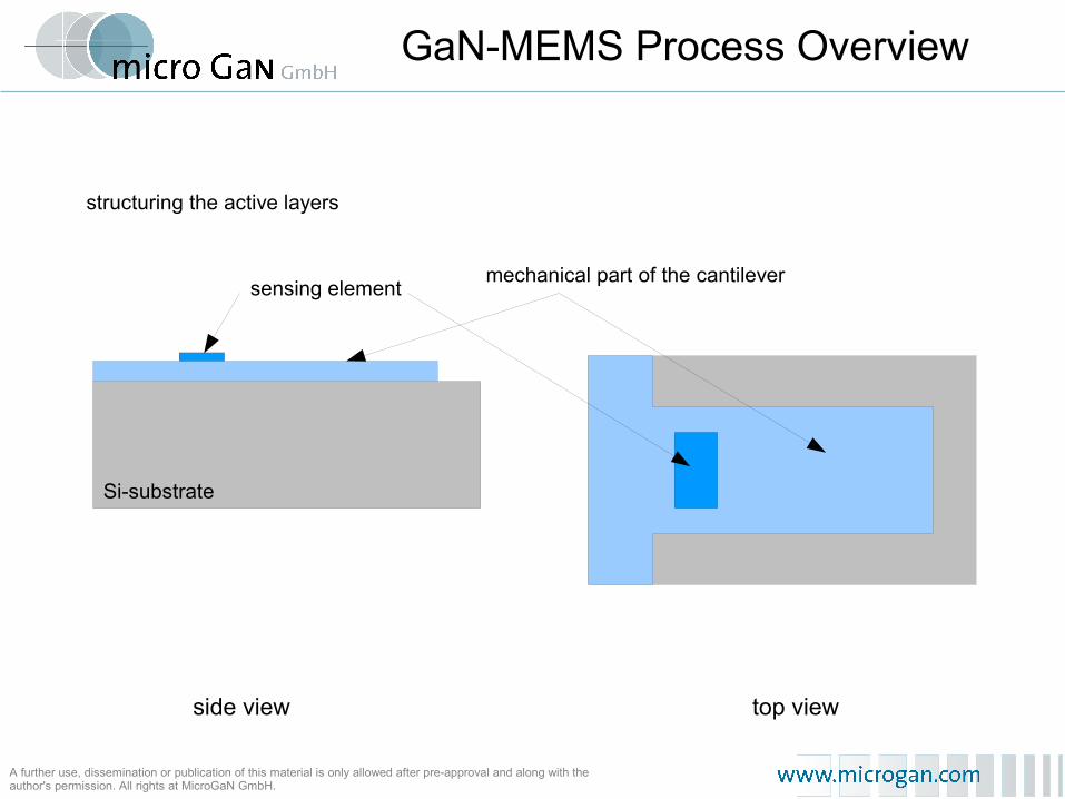
structuring the active layers
GaN-MEMS Process Overview
sensing element mechanical part of the cantilever
A further use, dissemination or publication of this material is only allowed after pre-approval and along with theauthor's permission. All rights at MicroGaN GmbH.
side view top view
Si-substrate
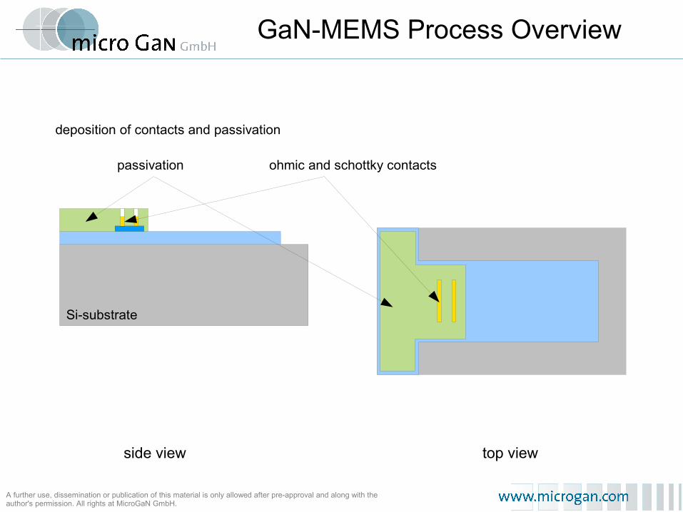
deposition of contacts and passivation
GaN-MEMS Process Overview
passivation ohmic and schottky contacts
A further use, dissemination or publication of this material is only allowed after pre-approval and along with theauthor's permission. All rights at MicroGaN GmbH.
side view top view
Si-substrate
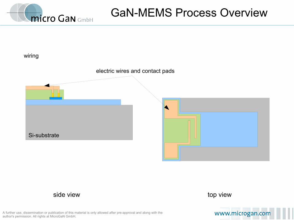
wiring
GaN-MEMS Process Overview
electric wires and contact pads

A further use, dissemination or publication of this material is only allowed after pre-approval and along with theauthor's permission. All rights at MicroGaN GmbH.
side view top view
Si-substrate
structuring the substrate
GaN-MEMS Process Overview
freestanding cantilever
silicon frame for mechanical stability

A further use, dissemination or publication of this material is only allowed after pre-approval and along with theauthor's permission. All rights at MicroGaN GmbH.
beam bent upwards
cantilever with a length of 750µm and a width of 200µm at room temperature
0,00 3,00 6,00 9,00 12,00 15,00 18,00 21,00 24,00 27,00 30,0030,00
35,00
40,00
45,00
50,00
55,00
60,00
65,00
Zeit (min)
Stro
m (µ
A)
0µm
20µm40µm
60µm80µm
100µm120µm
160µm
180µm
Cur
rent
(µA)
time (min)
deflection
Sensor signal vs time of a cantilever
Stability measurement

A further use, dissemination or publication of this material is only allowed after pre-approval and along with theauthor's permission. All rights at MicroGaN GmbH.
Sensor signal at high temperature
0 5 10 15 20 25 30 35 40 450
2
4
6
8
10
12
14
16
18
20
RT100°C200°C300°C
Auslenkung (µm)
rela
tives
Sig
nal (
%)
rela
tive
sens
or s
igna
l (%
)
deflection (µm)
beam bent upwards
Hotplate

A further use, dissemination or publication of this material is only allowed after pre-approval and along with theauthor's permission. All rights at MicroGaN GmbH.
500µm
GaN actuator beam
GaN is a polar material and lateral stress changes the polarization field
Theory predicts the change of the lattice constants by mani-pulating the polarization field. It should function as actuator.

A further use, dissemination or publication of this material is only allowed after pre-approval and along with theauthor's permission. All rights at MicroGaN GmbH.
Actuation with square wave voltages of different frequencies
Beam length: 800µmBeam width: 200µm
Amplitude: ~3,2µm
GaN actuator beam

A further use, dissemination or publication of this material is only allowed after pre-approval and along with theauthor's permission. All rights at MicroGaN GmbH.
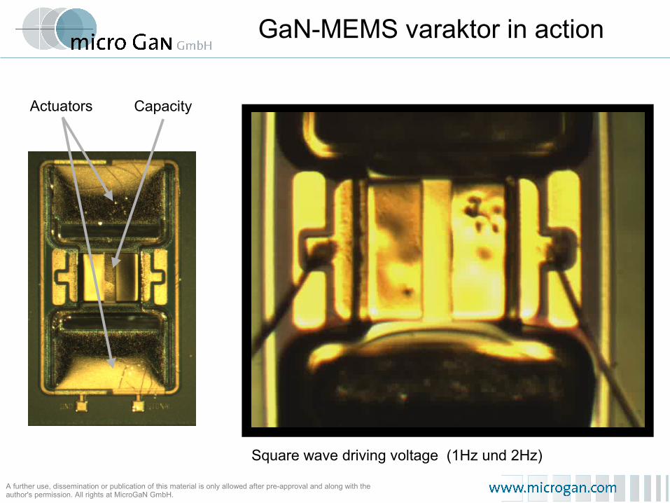
Actuators Capacity
Atuator
Actuator
Initial position (Cmin)
lower electrode actuated (Cmax)
RF-contact
Si-frame
sideview
GaN-MEMS Varaktor
A further use, dissemination or publication of this material is only allowed after pre-approval and along with theauthor's permission. All rights at MicroGaN GmbH.
Actuators Capacity
Square wave driving voltage (1Hz und 2Hz)
GaN-MEMS varaktor in action
A further use, dissemination or publication of this material is only allowed after pre-approval and along with theauthor's permission. All rights at MicroGaN GmbH.
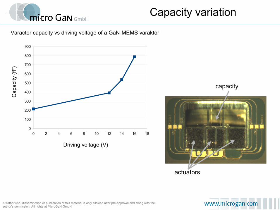
0 2 4 6 8 10 12 14 16 180
100
200
300
400
500
600
700
800
900
Aktorspannung (V)
Kap
azitä
t (fF
)C
apac
ity (f
F)
Driving voltage (V)
Varactor capacity vs driving voltage of a GaN-MEMS varaktor
actuators
capacity
Capacity variation

A further use, dissemination or publication of this material is only allowed after pre-approval and along with theauthor's permission. All rights at MicroGaN GmbH.
Conclusion
The piezoelectric effect in GaN opens the possibility for sensors with high signals on one hand.
On the other hand, turning the sensor principle upside down, the same material system functions as actuator.
This effect allows not only the applications discussed before, but also new fields of application where sensor and actuator are needed in combination.


