Page 1
MEMS Lens Scanners for Free-Space Optical Interconnects
By
Jeffrey Brian Chou
A dissertation submitted in partial satisfaction of the
Requirements for the degree of
Doctor of Philosophy
in
Engineering – Electrical Engineering and Computer Sciences
in the
Graduation Division
of the
University of California, Berkeley
Committee in charge:
Professor Ming C. Wu, Chair
Professor Bernhard Boser
Professor Liwei Lin
Fall 2011
Page 3
1
Abstract
MEMS Lens Scanners for Free-Space Optical Interconnects
by
Jeffrey Brian Chou
Doctor of Philosophy in Engineering – Electrical Engineering and Computer Sciences
University of California, Berkeley
Professor Ming C. Wu, Chair
Optical interconnects are the next evolutionary step for computer server systems, replacing
traditional copper interconnects to increase communication bandwidth and reduce overall power
consumption. A variety of implementation techniques to bring optics to the rack-to-rack, board-
to-board, and chip-to-chip scale are heavily pursued in the research space. In this dissertation we
present a micro-electro mechanical systems (MEMS) based free-space optical link for board-to-
board interconnects.
As with any free-space optical system, alignment is critical for the correction of undesired
vibrations or offsets. Thus our optical system implements a variety of MEMS based lens
scanners and opto-electronic feedback loops to maintain constant alignment despite both high
frequency and low frequency misalignments. The full implementation of all of the MEMS
devices is discussed, including the design, simulation, fabrication, characterization, and the
demonstration of the full optical link.
The first device discussed is an electrostatic lens scanner with an optoelectronic feedback loop
capable of tracking high frequency mechanical vibrations expected in computer server systems.
The second system discussed is an electrothermal lens scanner with mechanical brakes for long
term, large displacement, and zero power off-state tracking. Both linear and rotational actuators
are presented to correct for the major causes of misalignment measured in board-to-board
systems. A finite state machine based controller is demonstrated to act as the feedback loop
required to maintain alignment. A fully integrated packaging system is proposed for the
correction of all misalignment degrees of freedom. Finally, an alternative application of MEMS
lens scanners for light detection and ranging (LIDAR) for 3D imaging is explored, tested, and
simulated.
Page 4
i
Table of Contents
Table of Contents ............................................................................................................................. i
List of Figures ................................................................................................................................ iv
List of Tables ................................................................................................................................. xi
Acknowledgements ....................................................................................................................... xii
1. Introduction ............................................................................................................................. 1
1.1. History .............................................................................................................................. 1
1.2. Optical Interconnects for Blade Server Systems .............................................................. 2
1.3. Improving Cooling Efficiency ......................................................................................... 3
1.4. MEMS Based Optical Alignment .................................................................................... 4
1.5. Packaging – An Integrated Solution................................................................................. 5
2. Board-to-Board Optical Misalignment ................................................................................... 6
2.1. Telecentric Optical Setup ................................................................................................. 6
2.2. Tilt Based Correction ....................................................................................................... 8
2.3. Rotation Based Correction ............................................................................................. 10
2.4. Full 5-axis Correction Optical System ........................................................................... 11
2.4.1. Optical Setup and Measurement Method ................................................................... 12
2.4.2. Passive Alignment Measurements .............................................................................. 12
2.4.3. Active Alignment Measurements ............................................................................... 14
3. Background ........................................................................................................................... 17
3.1. Beam Steering ................................................................................................................ 17
3.2. Comb Drive Mass Spring System .................................................................................. 18
3.2.1. Lateral Stability / Pull-in ............................................................................................ 19
3.3. Thermal “U-Shaped” Actuators ..................................................................................... 20
4. Electrostatic High Frequency Tracking ................................................................................ 22
4.1. Optical MEMS Design ................................................................................................... 22
4.2 MEMS Design ................................................................................................................ 25
4.3 Device Fabrication ......................................................................................................... 26
4.4 Device Characterization ................................................................................................. 30
4.5 Experimental Results...................................................................................................... 33
5. Integrated VCSEL and Lens Scanner ................................................................................... 38
5.1 The Need for Integration ................................................................................................ 38
Page 5
ii
5.2 Design............................................................................................................................. 39
5.2.1 Large Range Scanner .................................................................................................. 39
5.2.2 Assembly .................................................................................................................... 43
5.2.3 Fabrication .................................................................................................................. 45
5.2.4 Assembly .................................................................................................................... 46
5.3 Experiment and Characterization ................................................................................... 47
5.3.1 Assembly Accuracy .................................................................................................... 47
5.3.2 Microlens Scanner ...................................................................................................... 48
5.4 Beam Collimation .......................................................................................................... 51
5.5 Summary ........................................................................................................................ 52
6. Electrothermal Linear Actuator ............................................................................................ 53
6.1 Introduction .................................................................................................................... 53
6.2 MEMS Design ................................................................................................................ 54
6.2.1 Spring Design ............................................................................................................. 54
6.2.2 Electrothermal U-Shaped Thermal Actuator .............................................................. 54
6.2.3 Electrothermal Stepper Actuator ................................................................................ 55
6.2.4 Bistable Break............................................................................................................. 57
6.3 Fabrication and Assembly .............................................................................................. 59
6.4 Experimental Results and Analysis ................................................................................ 60
6.5 Modeling ........................................................................................................................ 65
6.6 Finite State Machine (FSM) Control System ................................................................. 66
6.7 Long Term Testing ......................................................................................................... 70
6.8 10Gbps Free-Space Optical Link Test ........................................................................... 73
6.9 Summary ........................................................................................................................ 75
7. Electrothermal Rotational Actuator ...................................................................................... 76
7.1 Introduction .................................................................................................................... 76
7.2 Optical System ............................................................................................................... 77
7.3 Mems and Lens Design .................................................................................................. 78
7.4 Fabrication ...................................................................................................................... 79
7.5 Experimental Results...................................................................................................... 81
7.6 Summary ........................................................................................................................ 85
8. Future Steps: Advanced Applications ................................................................................... 86
8.1 Full Optical Assembly .................................................................................................... 86
8.2 Light Detection and Ranging (LIDAR) ......................................................................... 88
Page 6
iii
8.2.1 Introduction ................................................................................................................ 89
8.2.2 Experimental Results .................................................................................................. 91
8.2.3 FM Linearity & Simulation ........................................................................................ 92
9. Conclusion ............................................................................................................................ 96
10. Bibliography ......................................................................................................................... 98
Page 7
iv
List of Figures
Fig. 1.1. The historical roadmap for the integration of optical communication as a function of
time and bandwidth, versus link distance and transceiver cost [1]. ................................................ 2
Fig. 1.2. Images of the blade and chassis of a server system from [36]. (a) Image of a single
blade. (b) An empty chassis where the blades are inserted. The midplane is where the electrical
backplane is located and it clearly obstructs airflow. (c) Image of a blade partially inserted into
the chassis. ...................................................................................................................................... 3
Fig. 1.3. Schematic diagram illustrating the air flow path across a blade system from [43]. The
limited entrance and exit paths are limited to small backplane apertures. ...................................... 4
Fig. 2.1. Schematic of a traditional telecentric optical system. .................................................... 7
Fig. 2.2. Simple diagram of optical system. (a) Perfectly aligned board-to-board system. (b)
Misalignment of tilted board corrected by shifted lens scanner. .................................................... 8
Fig. 2.3. Measured spot locations of the telecentric optical system. (a) Displacement of spot as
the board is displaced along the y-axis. The discrete jumps are due to the discrete pixels used to
measure the telecentriclocation. (b) Displacement of spot as the board is tilted. ......................... 9
Fig. 2.4. Rotational misalignment correction via a double sided microlens array. (a) Shows the
default position of the entire system. (b) Shows the rotation of the microlens array rotating the
image of the VCSELS onto the detector plane. ............................................................................ 11
Fig. 2.5. Illustrations of misalignment schemes and their corresponding detector plane images,
using a single lens focusing system. The white boxes represent photodetectors. All of these
cases can be corrected with our optical system. (a) Perfectly aligned case. (b) Tilt
misalignment. (c) Lateral translation in the Y direction. (d) Lateral translation in the X
direction. (e) Rotation about the Z-axis (optical axis). (f) Translation in the Z direction, causes
the laser light to be defocused, which can lead to cross talk and lower power densities. ............ 12
Fig. 2.6. Lateral board displacement measurements. Due to the telecentric optical system, we
should see minimum displacement of the spots despite large board translations. (a) Shows the
measured beam spot displacement as a function of moving the receiving board along the X
direction. (b) The beam spot image at 0 mm displacement, and (c) beam spot image at 2.75 mm
displacement. ................................................................................................................................ 13
Fig. 2.7. Board tilt correction. (a) Spot displacement as a function of board tilting. The blue
solid line is obtained from geometric optics. (b) Beam spots at 0° board tilt. (c) Beam spots at
1.6° board tilt. Red dots indicate beam spot locations at 0° board tilt. ........................................ 14
Fig. 2.8. Array rotation via microlens array rotation. (a) The measured image rotation as a
function of the microlens array rotation. (b) Spot image at 0° rotation. (c) Spot image at 3°
rotation. ......................................................................................................................................... 15
Page 8
v
Fig. 2.9. (a) Beam spot location at 0° board tilt. (b) Beam spot location at 0.7° board tilt.
Spots are displaced by 157.4 μm from the original positions (red spots). (c) Spots are moved
back to 0° location with the millimeter lens displaced by 170 μm. .............................................. 15
Fig. 3.1. Basic beam steering principal. The image on the left shows a collimated LASER beam
emitting perpendincuarly to the lens. The image on the right shows the lens shifted by Δd, which
causes the beam to output at an angle θ = Δd/f. ............................................................................ 17
Fig. 3.2. Basic schematic of a mass spring, comb-drive system. Notation here will be used
throughout the dissertation. The red box indicates the unit finger. ............................................. 18
Fig. 3.3. Parallel plate analysis of side instability in comb drive systems. ................................. 19
Fig. 3.4. Basic schematic of a “U-Shaped” thermal actuator. Due to thermal bi-morph
deformation, this structure bends downward when current is applied through it. ........................ 21
Fig. 4.1. Schematic diagram of MEMS based free-space board-to-board optical interconnect.
Although the optical transmitter and receiver are laterally misaligned by Δx and Δθ, the MEMS
microlens scanner steers the optical beam to the correct position. ............................................... 23
Fig. 4.2. Differential driving scheme with each outer comb set DC biased at equal but opposite
voltages as indicated by the Vleft and Vright boxes. The inner shuttle is where the signal, Vshuttle, is
applied. .......................................................................................................................................... 25
Fig. 4.3. Simulated resonant frequencies of the MEMS structure with values of (a) 413 Hz in
the x-direction, (b) 782 Hz in the y-direction, and (c) 1799 Hz in the undesired rotational
direction. ....................................................................................................................................... 26
Fig. 4.4. Fabrication process flow of two-dimensional MEMS lens scanner. (a) SOI wafer (b)
DRIE front side isolation trenches on 20 µm device layer. (c-d) Deposit and pattern low-stress
nitride and polysilicon for electrical isolation. (e) DRIE for MEMS structures, such as
combdrives and springs. (f) DRIE backside through-wafer etching on 500 µm-thick silicon
substrate. (g) HF vapor for release etch on 1 µm-thick buried oxide layer. (h) Directly apply
ultraviolet-curable polymer on the lens frame, and cure for 5 minutes. ....................................... 27
Fig. 4.5. Scanning electron micrograph (SEM) and microscope images of the fabricated MEMS
devices. (a) SEM of the entire device after front side etching. (b) Zoom in on comb structures
and lens frame. The outer diameter of the lens frame is 300 µm. (c) An optical microscope
image of complete MEMS structure with polymer microlens. (The electrical isolation steps are
skipped.) ........................................................................................................................................ 29
Fig. 4.6. Scanning modes of operation for two orthogonal axes. Electrical isolation trenches are
indicated by thick black lines. The white areas indicate the applied voltage. ............................. 30
Fig. 4.7. Static characteristics of the MEMS lens scanner for its X-axis motion (Fig. 2(a)).
Measured and fitted MEMS displacement as a function of input voltage (VX). .......................... 31
Page 9
vi
Fig. 4.8. Simulated capacitance curves for comb drive fingers at different displacement values.
Negative displacement indicates disengaged comb drive fingers. (a) The simulated capacitance
vs. displacement curve. At 0 displacement, the curve becomes nonlinear. (b) The simulated
dC/dx curves to model the force of the comb drives. ................................................................... 32
Fig. 4.9. Static measurements of the double sided device for varying bias voltages. (a)
Simulated curves from FET analysis predict an unstable point at 0V input for bias voltages
greater than 10V. (b) Measured results confirm the simulations. Our device is biased at 10V to
ensure linear operation. ................................................................................................................. 32
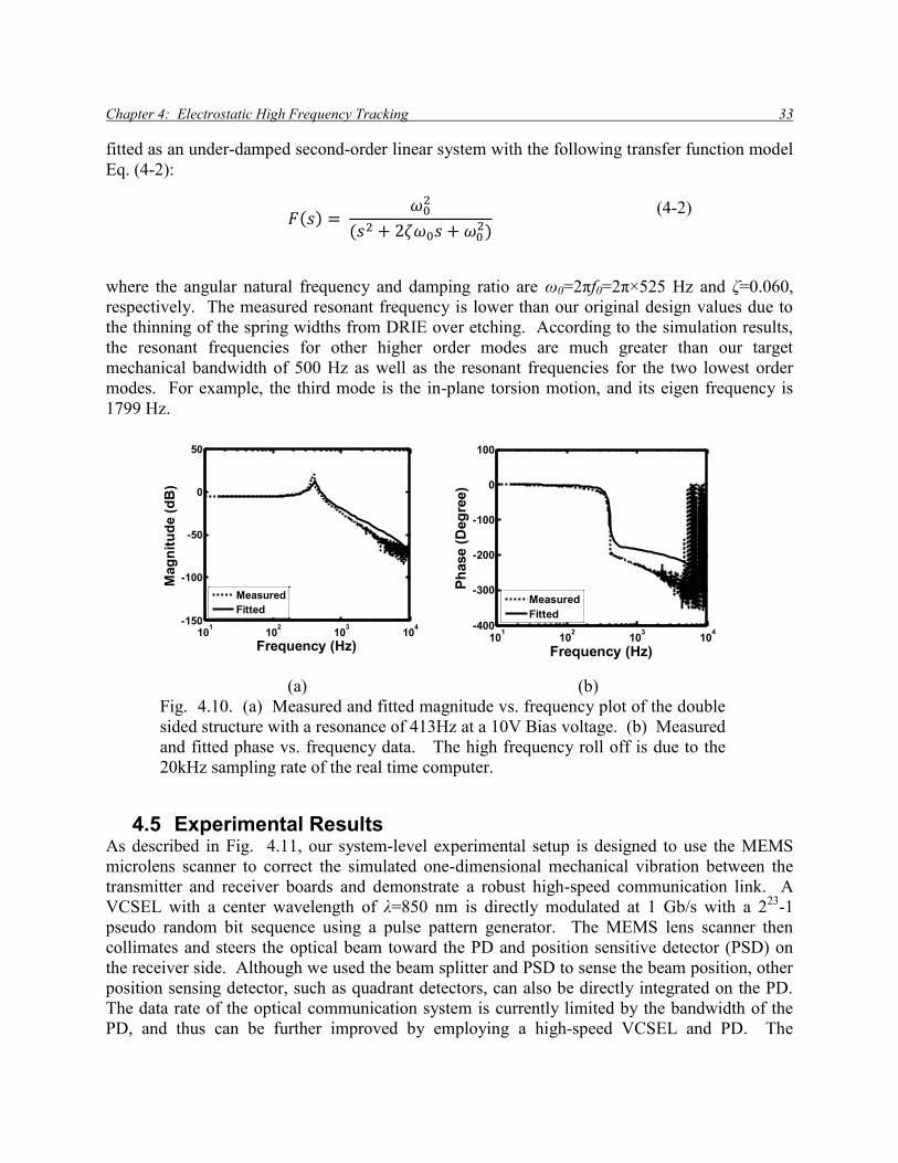
Fig. 4.10. (a) Measured and fitted magnitude vs. frequency plot of the double sided structure
with a resonance of 413Hz at a 10V Bias voltage. (b) Measured and fitted phase vs. frequency
data. The high frequency roll off is due to the 20kHz sampling rate of the real time computer. 33
Fig. 4.11. Schematic diagram of our experiment setup with a mechanical shaker for real beam
displacement. BS: Beam splitter. PPG: Pulse pattern generator at 1 Gbits/s. PD: high-speed
photodetector with 1 GHz 3-dB bandwidth. ................................................................................. 34
Fig. 4.12. Block diagram setup with electrically injected displacement, used for collecting the
closed loop frequency response data at high frequencies. ............................................................ 34
Fig. 4.13. Measured and simulated sensitivity magnitude plot with a 0 dB crossing at about 700
Hz, which reveals the noise suppression bandwidth. .................................................................... 36
Fig. 4.14. Eye diagrams obtained to demonstrate optical communication improvement with a 1
Gb/s modulation rate in the midst of a 10Hz noise signal. (a) The eye diagram is clear and open
in the perfectly aligned case. (b) The eye diagram is severely degraded with noise from the
mechanical shaker. (c) The eye is restored when the feedback is turned on. ............................. 37
Fig. 5.1. Schematic of MEMS scanner and alignment chip. The VCSEL is self-aligned to the
center of the lens shuttle. The red spheres are used to align and accurately separate the MEMS
chip from the VCSEL to be at the desired focal length for beam collimation. Wire bond pads for
the VCSEL are routed out and away from the center of the MEMS chip for external probing. .. 39
Fig. 5.2. Simplified drawing of the MEMS lens scanner with to-scale bending of the pre-bent
spring structures. The lens shuttle is shown bending to the (a) left, (b) center, and (c) right. Note
how certain springs condense and straighten up to increase the stiffness in the vertical direction.
....................................................................................................................................................... 40
Fig. 5.3. Simulated spring constants to determine maximum displacement before pull-in using
parameter values in Table 5.1. The kpre-bent and kstraight are a result of FEM simulations of the
entire MEMS shuttle for pre-bent and comparable straight springs, respectively. Dotted lines A
and B correspond to the experimentally observed maximum displacements for the straight and
pre-bent springs. ............................................................................................................................ 41
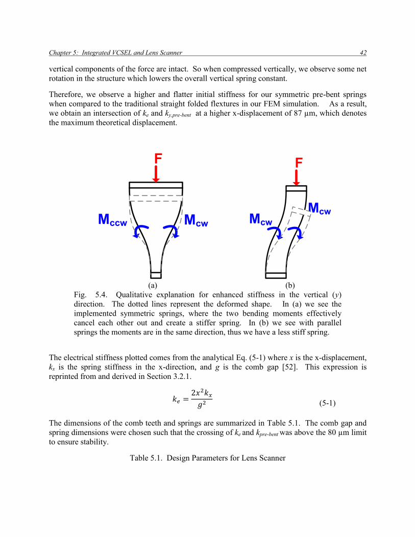
Fig. 5.4. Qualitative explanation for enhanced stiffness in the vertical (y) direction. The dotted
lines represent the deformed shape. In (a) we see the implemented symmetric springs, where the
Page 10
vii
two bending moments effectively cancel each other out and create a stiffer spring. In (b) we see
with parallel springs the moments are in the same direction, thus we have a less stiff spring. .... 42
Fig. 5.5. Cross sectional schematic of the assembly. Alignment spheres are used to align the
MEMS to alignment chip in the X,Y, and Z directions. ............................................................... 44
Fig. 5.6. Mask layout files for the (a) alignment chip, (b) backside MEMS through-wafer
etching, and (c) MEMS scanner. The full overlapped layout is shown in (d). ............................ 45
Fig. 5.7. Fabrication layout of the MEMS chip a)-d) and the alignment chip (e)-(h). Both chips
start with SOI wafers (a,e), then proceed with front side DRIE etch (b,f), followed by backside
through wafer etching (c). A wafer-saw process is performed for dicing (g). Due to aspect ratio
dependent etching, the smaller holes for the alignment spheres do not etch through the entire
wafer. Finally an HF vapor release etch is done to release the silicon from the oxide (d,h). ...... 46
Fig. 5.8. Photographs and SEM images of the MEMS and alignment chip. A photograph of the
fully assembled device is shown in (a). The VCSEL contact pads can be seen protruding from
the device in (b). An SEM image of the assembled chip is shown in (c). Using this image, we
measure the gap between the two chips to be 121±7 µm. (d) Shows the alignment chip with
alignment spheres and wire bonded VCSEL. (e) Shows a close up image of the wire bonded
VCSEL and the silicon blocks used to hold it in place. (f) Is a close up view of the precise
alignment sphere. .......................................................................................................................... 48
Fig. 5.9. Mask layout of the straight (a) and pre-bent (b) devices for displacement comparison.
Microscope image of the lens shuttle displaced 83 µm at 80V c). ............................................... 49
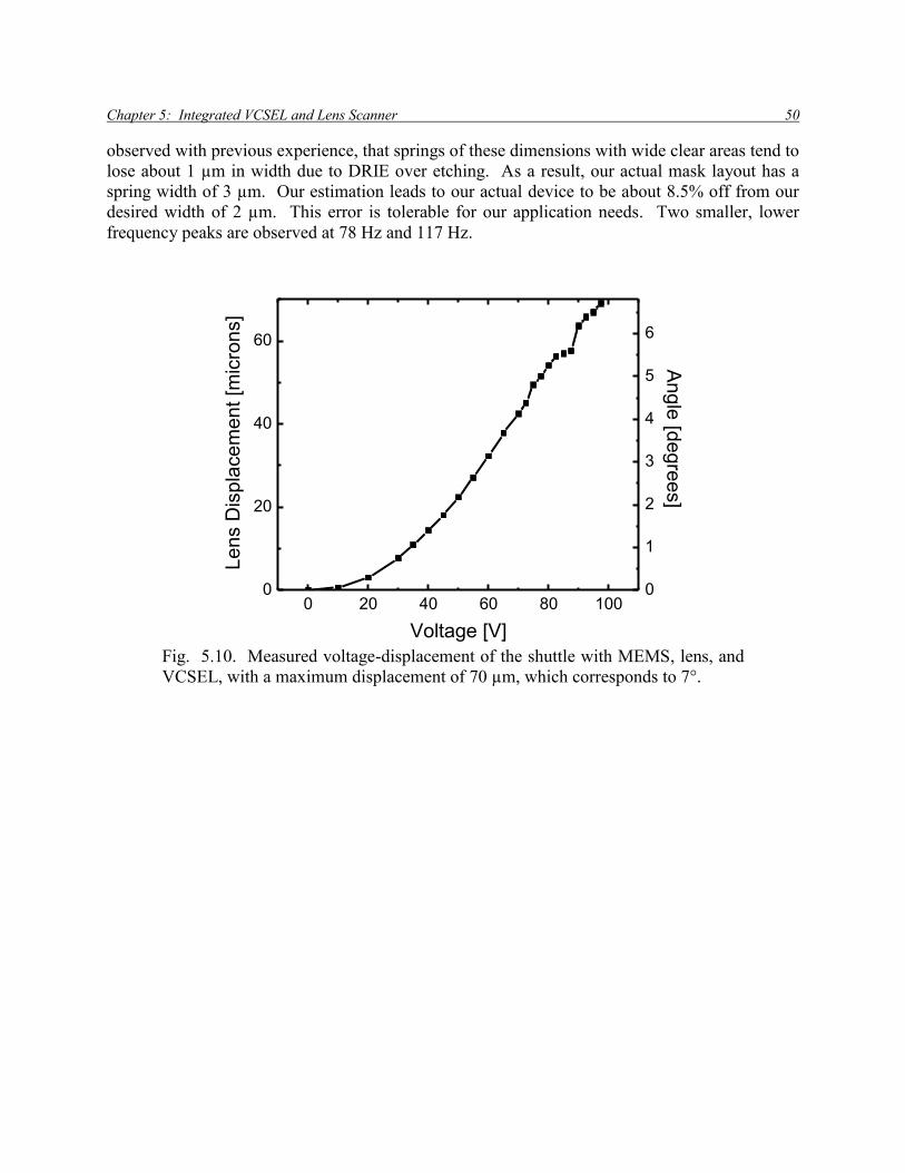
Fig. 5.10. Measured voltage-displacement of the shuttle with MEMS, lens, and VCSEL, with a
maximum displacement of 70 µm, which corresponds to 7°. ....................................................... 50
Fig. 5.11. Measured mechanical frequency response of the MEMS with lens. We observe a
peak resonance at 236 Hz. ............................................................................................................ 51
Fig. 5.12. Fitted curves to CCD beam profiles taken at reference 0mm, and 9mm away to
measure beam collimation. The half angle divergence is calculated by comparing the widths of
the two curves at the intensity value of 40, and has a value of 2.6°. ............................................ 52
Fig. 6.1. Schematic diagram of electrothermal lens scanner with bi-stable brakes. ................... 54
Fig. 6.2. Schematic and dimensions of the thermal actuators used in the MEMS stepper motor
design. This actuator is used for both the bistable brake and the stepper motor. The former uses
an extending leg and foot to enhance pushing displacement, as shown in the gray line. ............. 55
Fig. 6.3. Schematic view of stepper motor with two alternating pairs of thermal actuators
gripping and pushing the lens shuttle upwards. The light gray lines represent the engagement of
the second pair of actuators to the shuttle. The pivot point refers to the point at which the
actuators make contact with the shuttle and tends to roll about when pushing the shuttle........... 56
Fig. 6.4. Voltage timing diagram for the stepper motor. ............................................................ 57
Page 11
viii
Fig. 6.5. (a) Schematic of the curved bi-stable structure and brake pad used for the brake. The
light gray line represents the second stable state of the brake. The thermal actuators used to
toggle the brake are not shown here. (b) Schematic view of bi-stable structure with labels
corresponding to Table 6.1. .......................................................................................................... 58
Fig. 6.6. Fabrication steps (a) Front-side silicon etch. (b) Back-side through wafer etch. (c) HF
vapor release etch, which also causes automatic dicing, (d) Lens assembly on the MEMS
structure......................................................................................................................................... 59
Fig. 6.7. (a) Shuttle at 0 displacement. (b) Shuttle displaced by 170 µm, with a maximum
speed of 350 µm/s, and an initial step size of about 10 µm. ......................................................... 60
Fig. 6.8. (a) Bistable brake switched to the “open” state by two thermal actuators. (b) Brake
switched to the “closed” state, by two different thermal actuators. .............................................. 60
Fig. 6.9. (a) The shuttle is held with a displacement of 60 µm by the stepper actuators. (b)
Once the brake is released, the shuttle falls back to its equilibrium state. .................................... 61
Fig. 6.10. Optical setup used to obtain high resolution displacement plots of the lens scanner. 61
Fig. 6.11. Measured displacement of the MEMS/Lens system with varied applied voltages with
50ms step time. The upward sloping portion (t<4s), corresponds to the top set of actuators
moving the lens up, against gravity. The flat region immediately following (4s<t<4.7s),
corresponds to the bi-stable brake engaged and holding the shuttle in place. The large amplitude
ringing is the oscillation of the lens shuttle after the brakes are disengaged. The downward
sloping portion (t>5.6s) correspond to the bottom actuators moving the shuttle with gravity. The
last flat portion correspond to the brakes holding the shuttle in place. ......................................... 62
Fig. 6.12. High resolution view of the 30V stepper data with ts=50ms previously shown in Fig.
6.11. . (a) Shows the data in the time range 0s<t<0.5s. We see with each actuator step, the
shuttle is displaced by about 2.5 μm. With every other step, we see a ringing of about 230 Hz,
which occurs when the stepper transitions from 2 pairs of actuators to 1 pair. (b) Shows the data
in the time range 1s<t<1.5s. Only when two actuators are engaged does the shuttle move
upward, otherwise when only a single pair is engaged the shuttle remains in place. (c) Shows
the data in the time range 2.7s<t<3.2s. When both actuators are engaged we still obtain a
positive displacement, however when only a single pair is engaged, the shuttle moves slightly
backward. (d) Shows the data in the time when the brakes are disengaged and the entire shuttle
oscillates freely, revealing the resonant frequency of the suspension spring / lens system to be 50
Hz. ................................................................................................................................................. 64
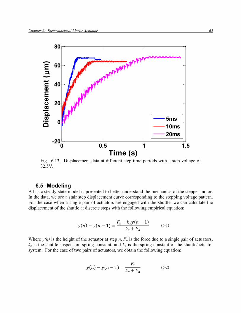
Fig. 6.13. Displacement data at different step time periods with a step voltage of 32.5V. ........ 65
Fig. 6.14. Simulated stepper displacement curve compared to measured data at 100ms stepper
time. Simulated data is modeled from the 50ms stepper data. The close comparison between the
two shapes confirms the validity of the model. ............................................................................ 66
Fig. 6.15. Finite state machine based control system for feedback position control. ................. 68
Page 12
ix
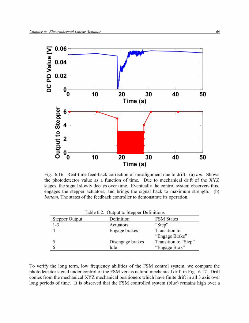
Fig. 6.16. Real-time feed-back correction of misalignment due to drift. (a) top, Shows the
photodetector value as a function of time. Due to mechanical drift of the XYZ stages, the signal
slowly decays over time. Eventually the control system observers this, engages the stepper
actuators, and brings the signal back to maximum strength. (b) bottom, The states of the
feedback controller to demonstrate its operation. ......................................................................... 69
Fig. 6.17. Photodetector intensity values as a function of time to compare uncorrected drift
based misalignment (red) to feedback controlled alignment (blue). ............................................. 70
Fig. 6.18. Microscope images of the teeth for long term reliability frictional testing. (a)
Unused and clean stepper teeth. (b) Stepper teeth after prolonged use. The point of contact
refers to the corner of which the stepper makes contact with the shuttle. (c) Brake teeth showed
very little sign of wear and tear as all of the teeth looked relatively intact. ................................. 71
Fig. 6.19. Thermal actuator comparison with free bending and pushing a rigid structure. (a)
Initial state of thermal actuator with zero current. (b) Actuator at 35 V with free bending, the
bending of the hot arm is small. (c) Actuator at 35 V pushing against the bi-stable structure, we
can see the bending of the hot arm is more severe. ...................................................................... 72
Fig. 6.20. (a) A single actuator at 35 V is shown, and is unable to flip the bi-stable structure.
(b) The black circle is a rigid probe tip and is pressed against the bulging region of the hot arm
and clearly the force is dramatically increased as the actuator has enough force to flip the bi-
stable structure. (c) Long term, permanent deformation of the actuators with zero volts. ......... 73
Fig. 6.21. (a) Optical table setup for the board-to-board experiment, with the copper mounted
VCSEL chips on the left and the high-speed photodetector (PD) on the right. (b) A close up
look of the MEMS chip mounted on PCB board, wire bonded, and soldered. ............................. 74
Fig. 6.22. (a) The board is tilted by 0.45 ° the signal is lost. (b) After the lens is displaced by
49 μm, we correct the tilt and re-establish the link. ...................................................................... 75
Fig. 7.1. (a) Schematic view of the board-to-board optical setup with tilt and lateral
displacement correction. (b) Rotational correction about the X axis by Δθ, the final spot image is
rotated by 2Δθ. Both schemes are designed to operate simultaneously, allowing up to 5 degrees
of freedom of correction. .............................................................................................................. 77
Fig. 7.2. Schematic of MEMS microlens array rotational stage. Clockwise (CW) and counter-
clockwise (CC) actuators rotate the lens array. ............................................................................ 79
Fig. 7.3. Fabrication process flow of the MEMS device. (a) SOI wafer with 50 μm device
layer, and 2 μm buried oxide layer. (b) DRIE entire front side device, single mask. (c) HF
vapor release etch. (d) Mount fabricated microlens array onto the MEMS device with UV
curable epoxy. ............................................................................................................................... 80
Fig. 7.4. Fabrication of a double-sided microlens array. (a) Bare glass wafer. (b) Coat and
pattern front and backside with spin-on Teflon. (c) Dice wafer. (d) Deposit microlenses on front
and back side. ................................................................................................................................ 81
Page 13
x
Fig. 7.5. Image of microlens array mounted on MEMS stage. Alignment is achieved with
corner micro-bumps. ..................................................................................................................... 81
Fig. 7.6. Profile views of the printed microlens arrays. (a) and (b) show two different rows of
printed microlenses on the same chip. Based on these images, the follow parameters are
measured: lens height = 60 µm, lens diameter = 250 µm, and the focal length = 300 µm.......... 81
Fig. 7.7. (a) MEMS stage rotation at full 2.3° clockwise and counter clockwise with attached
microlens array. (b) Brake engaged to hold the stage at a constant rotational angle while
dissipating zero power. ................................................................................................................. 82
Fig. 7.8. MEMS rotation as a function of time. A maximum displacement of 2.3° is achieved.
A quadratic best fit curve is fitted to the data. .............................................................................. 83
Fig. 7.9. Measured rotation of VCSEL array spots as a function of the microlens array rotation.
....................................................................................................................................................... 84
Fig. 7.10. Rotated spot images with double-sided microlens array. (a) Image with a 0° rotation.
(b) Image with a 4° rotation at a microlens rotation of 3°. .......................................................... 85
Fig. 8.1. Simplified schematic drawing of the proposed optical assembly................................. 87
Fig. 8.2. Basic operating principal behind the FMCW LIDAR system. ..................................... 89
Fig. 8.3. The sawtooth mixing between the local signal (black) and the delayed signal reflecting
from the object (red). .................................................................................................................... 90
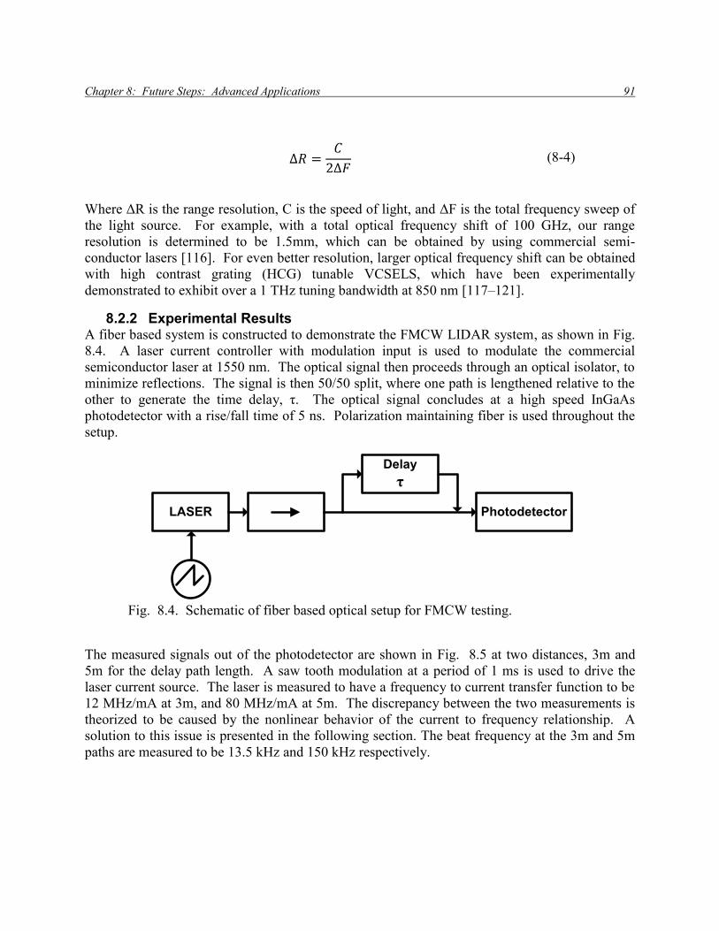
Fig. 8.4. Schematic of fiber based optical setup for FMCW testing. .......................................... 91
Fig. 8.5. Experimental results of the fiber-based LIDAR system. (a), (b) Show the frequency
domain analysis of the photodetector output at 3m and 5m respectively. (c), (d) Show the time
domain analysis of the output at 3m and 5m respectively. ........................................................... 92
Fig. 8.6. Optoelectronic phased lock loop for semiconductor laser linearization, reprinted from
[116]. ............................................................................................................................................. 93
Fig. 8.7. Matlab Simulink simulation of the optoelectronic PLL. (a) Shows the block diagram
of the feedback loop. (b) Shows the linear laser output frequency. (c) Shows the beat
frequency out of the photodetector matching the reference signal after about 0.02 ms. .............. 95
Page 14
xi
List of Tables
Table 2.1. Measured misalignments in blade server systems. Coordinates are in reference to
Fig. 2.2. ........................................................................................................................................ 10
Table 4.1. Design parameters for the electrostatic lens scanner. ................................................. 24
Table 5.1. Design Parameters for Lens Scanner .......................................................................... 42
Table 6.1. Bi-Stable brake design parameters ............................................................................. 57
Table 6.2. Output to Stepper Definitions ..................................................................................... 69
Table 8.1. Full assembly parameters............................................................................................ 87
Page 15
xii
Acknowledgements
I would like to thank my adviser and mentor Prof. Ming Wu for all of the years of
encouragement and understanding. What he saw in an innocuous undergraduate student all those
years ago I may never know, but I am thankful for the many opportunities he has provided for
me, both professionally and personally. His unwavering belief in me and my abilities has been
the fuel that has carried me through all these years.
The completion of this degree would also not have been possible without the collaborations and
friendships provided by others, past and present, in the 253M Cory office. Specifically, I would
like to thank Prof. Kyoungsik Yu, Niels Quack, Erwin Lau, Byung-Wook Yoo, Ming-Chun
(Jason) Tien, Sagi Mathai, Justin Valley, Prof. Aaron Ohta, Prof. Eric P.Y. Chiou, Arash
Jamshidi, Chris Chase, Roger Chen, Amit Lakhani, Chenlu Hou, Sapan Argawal, Owen Miller,
Nikhil Kumar, John Wyrwas, Frank Rao, James Farrara, Tae Joon Seok, Simone Gambini, and
Devang Parekh for their discussions, contributions, and friendships. A special thanks to our
collaborators at UC Davis, Prof. Dave Horsley and Brian Yoxall, and at HP labs, S.Y. Wang and
Michael Tan. I would also like to thank Prof. Bernhard Boser, Prof. Kris Pister, Prof. Luke Lee,
and Prof. Liwei Lin for serving on my graduate committees.
I would like to thank the UC Berkeley Nanolab staff for their hard work and dedication to
maintaining the machines. As well as my funding sources, including National Defense Science
and Engineering Graduate Fellowship (NDSEG), HP Labs, and DARPA.
Finally, I would like to thank my parents and brother for their constant support, love, and advice.
Page 16
Chapter 1: Introduction 1
1. Introduction
1.1. History Almost a century ago in 1915, the world’s first cross continental telephone call was placed
between Alexander Graham Bell in New York City and his one-time assistant Thomas Watson in
San Francisco. For the first time in human history, geographical barriers were torn down to
usher in a new era of human communication. What was the key invention behind such a
technological feat? The electrical amplifier, made with vacuum tubes, to maintain signal
integrity across long distances.
Today, users can enjoy high definition video conference calls with others all over the world,
while simultaneously managing their international stock portfolios. The information era is here,
truly shrinking the world into the palms of our hands. What was the key invention behind such a
technological feat? The optical link, made with glass and lasers, to maintain signal integrity
across long distances. Except this time, both the integrity and speed were improved by orders of
magnitude when compared to their electrical counterparts. In combination with advancements
with solid-state transistor technology, we have the modern day telephone, capable of global
communication with a swipe of a finger. Thus fundamentally changing the way we view the
world, commerce, and each other.
Currently, long distance optical links, spanning oceans and continents across the world, form the
backbone of modern telecommunication. The switch from electrical to optical communication
greatly increased the communication bandwidth and distance. However, the use of optics is not
just limited to long, inter-continental communication anymore. With increasing demand of high
bandwidth internet, higher and higher speeds are being required for shorter and shorter distances.
Optical links have already replaced electrical links when their bandwidth-distance product
Page 17
Chapter 1: Introduction 2
exceeds 100 Gb/s-m [1]. At this threshold value, the overall cost per unit distance is simply too
high to be done with electrical interconnects. Even if this value were to remain constant, the
increasing demand for bandwidth will force more and more interconnects to switch from
electrical to optical.
Fig. 1.1 shows the historical trend of optical links penetrating the market as a function of time
and bandwidth, which is reproduced from [1]. Clearly the general trend of optics is for shorter
and shorter distances as bandwidth demands increase [2–4]. It is projected in the future that
optics will be used for not only chip-to-chip communication but intra-chip applications as well
[3], [5–9], [9–13]. The focus of this dissertation, is the application of optical interconnects for
board-to-board systems, which is of more immediate use [6], [14–32].
Fig. 1.1. The historical roadmap for the integration of optical communication as
a function of time and bandwidth, versus link distance and transceiver cost [1].
1.2. Optical Interconnects for Blade Server Systems Optical interconnect technologies can significantly increase the chip-to-chip and board-to-board
communication bandwidth, relieving the bottleneck of traditional electrical backplane-based
computer systems [1], [5], [33], [34], [28], [27], [25], [35–38], [18], [39], [17]. Specifically,
free-space optical interconnects using arrays of vertical cavity surface-emitting lasers (VCSELs)
and photo-receivers allow for lower power and higher bandwidth alternatives to traditional
copper-based electrical interconnects. When compared to waveguide-based optical interconnect
technologies, free-space optical interconnects provide a number of advantages in communication
capacity, density, and scalability due to their parallelism.
Page 18
Chapter 1: Introduction 3
In Fig. 1.2(a) an image of a typical blade populated with a dense collection of components is
shown [36]. These blades are then inserted into the chassis and connect to a midplane, as in Fig.
1.2(b),(c). The midplane serves to be the main electrical communication pathway between all
blades, and is thus composed of a communication wiring. The high density of blades makes the
compact size of free-space optical interconnects more attractive than cabled systems, since the
overall wire lengths can be reduced. The total communication path length between two boards
can be reduced from 30 cm to 2.5 cm with a free-space optical system. With the wiring
bandwidth proportional to A/L2
, where A is the wire cross sectional area, and L is the length of
the wire, the long length of board-to-board systems fundamentally limits the maximum
bandwidth of wires [40]. The only available option is to make wires wider, but this is highly
undesirable as board real estate is already very limited. Optical interconnects have no such
bandwidth limits and can achieve speeds of up to 1 Tb/s.
(a) (b) (c)
Fig. 1.2. Images of the blade and chassis of a server system from [36]. (a)
Image of a single blade. (b) An empty chassis where the blades are inserted.
The midplane is where the electrical backplane is located and it clearly obstructs
airflow. (c) Image of a blade partially inserted into the chassis.
In 2009 the power consumption of a typical blade is reported to be 340 W, and it is estimated a
total of 136 W is consumed by communication on the blade alone. With optical communication,
an estimated 7% power reduction is possible; with a projected 42 million servers in 2012, this
translates to $1.2 billion in total energy savings across the world [41].
1.3. Improving Cooling Efficiency A path to increased power savings of free-space optical interconnects is revealed in the cooling
systems. By eliminating cables, both electrical and optical, free-space interconnects can reduce
clutter and increase the air cooling efficiencies in servers. Specifically, server backplane and
midplane sections severely limit the air flow allowed into each blade, as can be seen in Fig.
1.2(b) [42]. By removing these barriers, free-space interconnects can allow for power efficient
architectures, thus reducing both interconnect and cooling power needs. A study of blade server
cooling systems, by Rambo et al., shows the limited air flow path across a server in Fig. 1.3
[43]. A maximum flow rate of 455 cubic feet per minute are needed to flow across the CPU to
Page 19
Chapter 1: Introduction 4
keep it at a maximum temperature of 52°C. To achieve this, the cooling fans draw a power of
120 W per fan [42]. Since the backplane airflow passageways make up only 14% of the total
midplane surface area, the fan cooling efficiency is severely degraded. With free space
interconnects, the entire backplane can be removed thus significantly increasing the airflow and
cooling efficiency.
Fig. 1.3. Schematic diagram illustrating the air flow path across a blade system
from [43]. The limited entrance and exit paths are limited to small backplane
apertures.
For even further cooling applications, blade server architectures can be changed completely, as
proposed in [36]. New schematics with no backplane can increase the density and cooling
efficiency for future designs that will lead to faster and lower cost systems.
1.4. MEMS Based Optical Alignment With advantages of bandwidth, size, and power consumption, free-space optical interconnects
provide an important alternative to traditional backplane electrical systems. However, alignment
between the optical source and detector is critical for high-performance, reliable optical
interconnect applications. Both high frequency mechanical noise, due to vibrations, thermal
drift, and low frequency mechanical noise, due to board insertions, have prevented the wide
deployment of such technology. Optical misalignment introduces higher insertion loss and
Page 20
Chapter 1: Introduction 5
crosstalk between optical links, which can severely impact the system performance and
reliability [36].
Various strategies to adaptively compensate for the misalignment in free-space board-to-board
optical interconnects have been demonstrated, including bulk optic Risley prisms [44], [27],
mechanical translational stages [45], liquid crystal spatial light modulators [46], [33], and
microelectromechanical systems (MEMS) devices [47], [48]. Among these approaches, MEMS
technology offers faster speed, low optical loss, and small form factor that can be directly
integrated on top of VCSEL arrays. In this dissertation we present two MEMS solutions, the
first concerns a vibration-resistant free-space optical interconnect system with an intensity-
modulated optical beam using real-time opto-electronic feedback control. The second, concerns
large displacements of bulk millimeter scale lenses with zero power, mechanically locked
positioning capabilities. Both of which are demonstrated with full free space optical links and
measured eye diagrams to show functional optical links.
1.5. Packaging – An Integrated Solution The high density of components on server blades makes real estate a precious commodity. For a
MEMS based free-space link, an integrated solution where the entire lens, MEMS, VCSEL, and
interconnects are compactly packaged together is a necessity for practical implementation. For
commercial needs, this packaging process should also be simple and low cost, thus the need for a
self-aligned process is most desirable. In this dissertation we demonstrate a simple packaging
and alignment strategy for the integration of optical MEMS components.
Page 21
Chapter 2: Board-to-Board Optical Misalignment 6
2. Board-to-Board Optical
Misalignment
2.1. Telecentric Optical Setup The traditional, simplified telecentric optical system is shown in Fig. 2.1. The system consists
of two collimating lenses with an aperture stop at the center between the lenses. The primary
advantage of this system is the magnification on the photodetector array is independent of the
board separation distance. The aperture stop serves to only allow the chief rays (center rays) of
the transmitting VCSEL to be imaged on the photodetector array. By doing so, the quality of the
focus is maintained, despite variable board separation (VCSEL and photodetecor). The
telecentric system also allows for ideally perfect re-imaging of the VCSEL plane onto the
photodetector array plane. Meaning the light is reimaged on the photodetector plane with zero
incident angle shift. For these reasons, a popular application of telecentric systems is machine
vision, where object distance can vary drastically, and sharp focus onto a planar photodetector
are critical [49]. In more traditional, non-simplified systems, telecentric lenses are composed of
many lenses in series in order to generate high-quality images.
Page 22
Chapter 2: Board-to-Board Optical Misalignment 7
Y
XZ
ApertureVCSEL
Array
Photodetector
Array
Fig. 2.1. Schematic of a traditional telecentric optical system.
The general optical setup used in our MEMS based free space optical link is shown in Fig.
2.2(a), with a MEMS mounted transmitting lens and a fixed receiving lens [36]. The VCSEL
array source is placed at the back focal plane of the transmitting lens and is reimaged onto the
detector plate, p2. The aperture stop is not used in our system in order to simplify the
components necessary for our design. An advantage to this optical setup is its immunity to
lateral displacements. Using Fourier optics, it can be explained by noticing a shift in the X-Y
plane or Z direction of the imaging plane will not change the input angle of the collimated input
light. As a result, the location of the focal point, or the Fourier transform of the light due to the
lens, will not be affected. Previous results demonstrate a tolerance of ±1mm board translation
with no degradation in communication [36]. There will of course be clipping losses if the
displacement is larger than the lens diameter, but we will assume we are working with relatively
small distances.
Page 23
Chapter 2: Board-to-Board Optical Misalignment 8
p1 p2
f1 2f1f1
VCSEL
Array
4-f Optics
Photodetector
Array
Transmitting Board Receiving Board
MEMS Lens
Scanner
Y
X Z
(a)
p1 p2
f1 2f1 f1
VCSEL
Array
4-f Optics
Photodetector
Array
Transmitting BoardReceiving Board
θ
MEMS Lens
Scanner
(b)
Fig. 2.2. Simple diagram of optical system. (a) Perfectly aligned board-to-
board system. (b) Misalignment of tilted board corrected by shifted lens
scanner.
2.2. Tilt Based Correction The major cause of misalignment in board-to-board systems comes from board tilting, as shown
in Fig. 2.2(b). Unlike lateral displacements, a tilting error introduces an angular offset into the
Page 24
Chapter 2: Board-to-Board Optical Misalignment 9
incoming light, thus shifting the focal point away from the detector and breaking the optical link.
To correct this error, transmitting lens is scanned in parallel to the board, steer the beam to match
the angle of the board tilt, and cause the beams to fall back onto the detectors. We
experimentally verify the lateral and tilt error by measuring the displacement of the beam spots
in Fig. 2.3, and find the maximum tolerable tilt to be 0.1°. The two MEMS devices both
translate lenses in this fashion, and correct for both dynamic and static board tilting
misalignments.
(a) (b)
Fig. 2.3. Measured spot locations of the telecentric optical system. (a)
Displacement of spot as the board is displaced along the y-axis. The discrete jumps
are due to the discrete pixels used to measure the telecentriclocation. (b)
Displacement of spot as the board is tilted.
The measured misalignment errors in blade server systems are listed in Table 2.1 [36]. Vibration
errors were found to be negligible and had displacement values less than 1 μm. This is expected
due to the large mass of the blades themselves as well as the tight mechanical locking of the
blades. Static misalignments in the X and Y directions due to board insertions are also within
tolerable limits with the telecentric optical setup, assuming we have large enough lenses to
prevent clipping loss. Static board tilt server chassis, as in Fig. 2.2(b), were measured to be
0.4°, which is larger than the tolerable limit of 0.1°. Correcting the tilt error is the primary
source of error this dissertation will address.
0 0.5 1 1.5 2 2.5 30
5
10
15
20
25
30
Telecentric Lateral Shift
Board Translation (mm)
Dis
pla
cem
en
t o
f S
po
t (
m)
0 0.5 1 1.5 20
100
200
300
400
Tilt Error
Board Tilt (deg)
Dis
pla
cem
en
t o
f S
po
t (
m)
Page 25
Chapter 2: Board-to-Board Optical Misalignment 10
Table 2.1. Measured misalignments in blade server systems. Coordinates
are in reference to Fig. 2.2.
Misalignment Error Magnitude
Vibrations < 1 μm
Static Δy 20 μm
Static Δx 200 μm
Board Tilt < 0.4°
2.3. Rotation Based Correction The final source of misalignment for our array based optical system is array-to-array rotation
about the z-axis in Fig. 2.2 (a). The final assembled photodetector and VCSEL array chips will
be manufactured and mounted independently, which may cause the two array boards to be
rotated relative to each other. To correct for this error, we utilize a double sided microlens array
placed a focal distance away from the VCSEL array, as in Fig. 2.4 (a). When the microlens
array is rotated about the z-axis, it will rotate the image of the VCSEL array on plane p1, which
is then translated to the photodetector array via the telecentric optical system, as in Fig. 2.4 (b).
The double sided microlens array is itself an array of telecentric optical systems with individual
microlenses for each VCSEL. As we displace the entire lens array relative to the VCSEL array
by Δy in Fig. 2.4 (b), we obtain a displaced image by 2Δy. The reason is due to the fact that the
thickness of the double microlens array is equal to twice the focal length, thus the y-distance
traveled is θd2f, where θd is the angle of the incident light after passing through the first lens, and
f is the focal length of the microlens. As a result, for small angles, we obtain a factor of 2
enhancement for the final rotated image. So if we rotate the microlens array by 1°, we should
obtain an image of the VCSELs spots rotated by 2°.
Page 26
Chapter 2: Board-to-Board Optical Misalignment 11
p1 p2
f2 2f2 f2f1 f12f1
Rotation
VCSEL
Array
4-f Optics
Photodetector
Array
Transmitting Board Receiving Board
Translation
Y
XZ
(a)
f2 2f2 f2f1 f12f1
Δθ2Δy
2Δy
2Δθ
Transmitting Board Receiving Board
Rotation
(b)
Fig. 2.4. Rotational misalignment correction via a double sided microlens array. (a)
Shows the default position of the entire system. (b) Shows the rotation of the
microlens array rotating the image of the VCSELS onto the detector plane.
2.4. Full 5-axis Correction Optical System With our full optical setup shown in Fig. 2.4, we are capable of simultaneously correcting all
five forms by using the telecentric optical setup to correct for lateral misalignments, lens
scanning for tilt misalignments, and microlens rotation for rotational misalignments. A graphical
summary of the five different alignment issues is shown in Fig. 2.5. To verify our optical setup
we construct the full optical setup, including a custom made double sided micro-lens array.
Page 27
Chapter 2: Board-to-Board Optical Misalignment 12
Y
XZ
(a) (b) (c)
(d) (e) (f)
Fig. 2.5. Illustrations of misalignment schemes and their corresponding detector
plane images, using a single lens focusing system. The white boxes represent
photodetectors. All of these cases can be corrected with our optical system. (a)
Perfectly aligned case. (b) Tilt misalignment. (c) Lateral translation in the Y
direction. (d) Lateral translation in the X direction. (e) Rotation about the Z-axis
(optical axis). (f) Translation in the Z direction, causes the laser light to be
defocused, which can lead to cross talk and lower power densities.
2.4.1. Optical Setup and Measurement Method The full optical system in Fig. 2.4(a) is reconstructed in a 30 mm cage system with manual
micrometer scanners used to simulate MEMS actuators. A 1x4 VCSEL array with center
wavelengths of 850 nm is placed at the back focal plane of the microlens array. The 4x4
microlens arrays lenses have dimensions D1≈250μm and f1≈250μm. The millimeter scale lens at
the “Translation” location has dimensions D2=6.33mm and f2=13.86mm. A gray-scale CCD
camera with 8.4 μm × 9.8 μm pixel dimension is used to record the optical intensity distribution
at the detector plane. Beam spot locations are determined by the location of the peak intensity
values of each spot. An optical filter is inserted to reduce the optical power so as to not saturate
the CCD signal. We assume that the radius of a 10 Gbps photodetector is 25μm, and any spot
displacement above this value will be considered a lost link.
2.4.2. Passive Alignment Measurements To experimentally verify that our full optical system still benefits from the telecentric optical
system reported previously [36], we measured the beam spot displacements due to lateral
translation and board tilting. Fig. 2.6(a) shows the measured results of scanning the receiving
board in the X direction and the corresponding displacement of the beam spots. We can see that
even at 2.75 mm board displacement, the maximum beam spot displacement is measured to be
less than 20 μm, well within the tolerable limit of 25 μm. Due to the circular symmetry of the
system, similar results are achieved for Y-axis displacements. Fig. 2.7(a) shows the measured
beam spot locations as a function of the board tilting. At a board tilt of 0.1°, the beam spot
locations are at 24.2 μm, which is at the cusp of the tolerable limit. Although not shown here,
the passive telecentric system is also immune to misalignments due to Z-axis (optical axis) board
displacements. After displacing the receiving board by several millimeters, no noticeable change
Page 28
Chapter 2: Board-to-Board Optical Misalignment 13
was detected at the detector plane. This can be attributed to the small divergence of the
collimated light propagation between boards. The key parameter to a successful telecentric
optical setup is placing the VCSEL and photodetector arrays precisely at their corresponding
focal points. Once this is achieved, the system will benefit from all passive alignment schemes.
(b)
(a) (c)
Fig. 2.6. Lateral board displacement measurements. Due to the telecentric
optical system, we should see minimum displacement of the spots despite large
board translations. (a) Shows the measured beam spot displacement as a function
of moving the receiving board along the X direction. (b) The beam spot image at
0 mm displacement, and (c) beam spot image at 2.75 mm displacement.
0 0.5 1 1.5 2 2.5 30
5
10
15
20
Board Translation (mm)
Dis
pla
cem
en
t o
f S
po
t (
m)
Spot 1
Spot 2
Spot 3
Spot 4
Page 29
Chapter 2: Board-to-Board Optical Misalignment 14
(b)
(a) (c)
Fig. 2.7. Board tilt correction. (a) Spot displacement as a function of board tilting.
The blue solid line is obtained from geometric optics. (b) Beam spots at 0° board
tilt. (c) Beam spots at 1.6° board tilt. Red dots indicate beam spot locations at 0°
board tilt.
2.4.3. Active Alignment Measurements Rotational misalignments between the VCSEL and detector arrays due to assembly errors can be
corrected by rotating the double-sided microlens array. Fig. 2.8 (a), (b) show the rotated image
of the VCSEL array as a function of rotating the microlens array. At a 3° microlens array
rotation, the image rotates by 4°, which is caused by the 2f1 thickness of the microlens array. If
the microlenses were fabricated to the targeted design specifications, there should be a factor of 2
enhancements for small angles between the imaged array and the rotated microlenses. Here the
enhancement is only 4/3 due to imperfect microlens fabrication.
0 0.5 1 1.5 20
100
200
300
400
500
Board Tilt (deg)
Dis
pla
cem
en
t o
f S
po
t (
m)
Spot 1
Spot 2
Spot 3
Spot 4
Theory
Page 30
Chapter 2: Board-to-Board Optical Misalignment 15
(b)
(a) (c)
Fig. 2.8. Array rotation via microlens array rotation. (a) The measured image rotation
as a function of the microlens array rotation. (b) Spot image at 0° rotation. (c) Spot
image at 3° rotation.
Board tilting errors can be corrected for by translational lens scanner. Fig. 2.9 shows a board tilt
of 0.7° being corrected by a 170 μm scan of the millimeter lens, which is the maximum
displacement achievable by our MEMS device. The maximum correctable board tilt angle by
the MEMS is determined by θ=Δy/f2, thus we can increase the total correctable board tilt with
shorter focal length lenses. For example, a focal length of 6.1mm corresponds to a maximum
angle of 1.6° [4].
(a) (b) (c)
Fig. 2.9. (a) Beam spot location at 0° board tilt. (b) Beam spot location at 0.7° board
tilt. Spots are displaced by 157.4 μm from the original positions (red spots). (c) Spots
are moved back to 0° location with the millimeter lens displaced by 170 μm.
We successfully demonstrate the feasibility of our MEMS integrated optical setup for board-to-
board optical interconnects with simultaneous alignment corrections of up to 5 degrees of
freedom. Our MEMS system is able to correct board tilt of 1.6° of board tilt, and VCSEL
image rotation of 2.3°, more than sufficient to address all major forms of misalignment in free-
space board-to-board systems.
0 0.5 1 1.5 2 2.5 30
1
2
3
4
5
Microlens Array Rotation (deg)
Imag
ed
Sp
ot
Ro
tati
on
(d
eg
)
y = 1.3*x + 0.075
Measured
Fitted
Page 31
Chapter 2: Board-to-Board Optical Misalignment 16
Page 32
Chapter 3: Background 17
3. Background
3.1. Beam Steering The fundamental concept behind the MEMS lens scanners is the ability to control the angle of
the light passing through the collimating lens. By shifting the lens relative to the VCSEL source,
we are able to control the output angle, as shown in Fig. 3.1.
VCSEL VCSEL
f f
Δd
θ
Fig. 3.1. Basic beam steering principal. The image on the left shows a
collimated LASER beam emitting perpendincuarly to the lens. The image on
the right shows the lens shifted by Δd, which causes the beam to output at an
angle θ = Δd/f.
Under the paraxial approximation, the angle of the output light can be calculated from Eq. (3-1).
The MEMS devices discussed in this dissertation, involve changing Δd and thus changing the
Page 33
Chapter 3: Background 18
angle of the output light. The effective angle is also inversely proportional to f, and thus a short
focal length lens is most desirable.
(3-1)
3.2. Comb Drive Mass Spring System Due to the extensive literature on comb drives, derivations and details will be left out of this brief
explanation. A more in depth analysis can be found in William Tang’s original comb drive
paper [50]. Fig. 3.2 shows the basic comb drive system.
g
lf
kx
Movable Comb
Drive
m
tf: finger thickness
Fixed Comb Drive
X
Y
Fig. 3.2. Basic schematic of a mass spring, comb-drive system. Notation here
will be used throughout the dissertation. The red box indicates the unit finger.
The force between the two sets of comb drives can be calculated by Eq. (3-2). Where N
corresponds to the number of unit fingers, ε0 is the permittivity of free space, V is the voltage
applied between the two structures, and g is the gap between the fingers.
(3-2)
The resonant frequency of this structure can be derived from the harmonic oscillator solution,
and is shown in Eq. (3-3). Where k is the effective spring constant, and m is the mass of the
moving shuttle. Later we will see that the mass of the lens is part of the shuttle mass, and thus
smaller and lighter lenses are preferable for more responsive systems.
√
(3-3)
Page 34
Chapter 3: Background 19
3.2.1. Lateral Stability / Pull-in The comb-drive system is susceptible to unstable pull-in conditions, as in simple electrostatic,
parallel plate systems. In these unstable cases, comb teeth will snap together in the y-direction
and cease to displace in the x-direction, as in Fig. 3.2. In the y-direction, the comb fingers are
simply double sided, parallel plates. To better illustrate our pull-in analysis, the comb fingers are
redrawn in a parallel plate fashion in Fig. 3.3.
ky
g0g
Fig. 3.3. Parallel plate analysis of side instability in comb drive systems.
Qualitatively, a system is stable when the total energy of the system has a local minimum at
which the system can be in. If no such minimum exists, then the entire system will be unstable
as the system attempts to rest at the lowest possible energy state, which is infinity in this case.
With this definition in mind, we first obtain the total energy in the parallel plate system.
(3-4)
Where the first term is the electrostatic energy as a function of ε, the permittivity of free space,
A, the cross-sectional area, g, the gap space, and V, the voltage applied between the plates. The
second term is the potential energy of the displaced spring as defined by Hooke’s law, where ky is
the spring stiffness in the y-direction, and g0 is the initial gap spacing.
Page 35
Chapter 3: Background 20
For a system to have a local minimum, the potential energy must be concave up. This implies
that the second derivative of the energy must be greater than zero. With this in mind, we
differentiate Eq. (3-3) twice.
(3-5)
From here we can define the minimum value of ky needed to ensure stability.
(3-6)
Since our real system is a comb drive system, we multiply by 2 to represent the double sided
nature of our structure, as well as by N, which is the total number of comb teeth.
(3-7)
If we now substitute Eq. (3-2) into Eq. (3-7), we obtain,
(3-8)
The term on the right side has units of N/m and can be thought of as an equivalent “electrical”
stiffness, or ke. Thus stability can be maintained as long as ky is greater than the electrical
stiffness. Clearly, we see that as the displacement of the comb drive increases in the x-direction,
the conditions for stability decrease exponentially, as the x2 term suggests. The common method
to mitigate this effect, is to simply increase the gap spacing, however this leads to higher
voltages to achieve the same displacement. Alternatively, previous researches have used pre-
bent or tilted beam structures to increase the value of ky over large displacements to enhance the
maximum x-displacement [51], [52].
3.3. Thermal “U-Shaped” Actuators The basic structure of the thermal actuator is shown in Fig. 3.4, with a thin arm defined by wh,u,
and a wide arm defined by wc,u [53–56]. The resistance is proportional to the cross-sectional area
and length, which causes the thin arm to have higher resistance than the wide arm. Since these
two effective resistors are in series, when current is passed through the structure, the thin arm
heats up due to joule heating, thermally expands, and bends the entire structure towards the
wider, cool arm. The thin section (ls,u) after the wide arm is meant to be compliant to increase
the bending displacement of the actuator. Theoretical analysis of thermal actuators can be found
in several references, including [55], [57], [58].
Page 36
Chapter 3: Background 21
lu
lc,uls,u
wc,u
wh,uguws,uiin
iout
Factuator
Fig. 3.4. Basic schematic of a “U-Shaped” thermal actuator. Due to thermal
bi-morph deformation, this structure bends downward when current is
applied through it.
Page 37
Chapter 4: Electrostatic High Frequency Tracking 22
4. Electrostatic High Frequency
Tracking
4.1. Optical MEMS Design Fig. 4.1 shows the schematic view of our proposed free-space optical interconnect system
correcting a lateral and tilt board misalignment (Δx and Δθ) by steering the optical beam path
across the board-to-board gap with a MEMS microlens scanner [59–62]. The beam scanning
range on the receiving board is amplified by the board-to-board distance, allowing for small
microscale lens scanning to compensate for larger lateral misalignments. This section assumes
an optical interconnect setup with one microlens scanner per VCSEL to avoid the use of large
optics on the MEMS translational stages and thus allow for higher operating speeds. We also
assume the misalignments are constrained in only one dimension along the X axis as shown in
Fig. 4.1. However, it is possible to extend our design for other optical configurations where
multiple VCSELs are relayed by a bigger lens or multiple intermediate lenses [6]. It is also
straightforward to improve our devices to scan two orthogonal axes as discussed in Section 4.3.
Page 38
Chapter 4: Electrostatic High Frequency Tracking 23
Fig. 4.1. Schematic diagram of MEMS based free-space board-to-board optical
interconnect. Although the optical transmitter and receiver are laterally
misaligned by Δx and Δθ, the MEMS microlens scanner steers the optical beam to
the correct position.
The microlens scanner design is based on the chosen parameters for board-to-board interconnects
summarized in Table 4.1. In our optical design, the light source (VCSEL) is located near the
back focal plane of the polymer microlens with a focal length of f. Assuming Gaussian beam
propagation, we calculate the minimum lens diameter given the VCSEL wavelength and board-
to-board spacing listed in Table 4.1. To collimate the beam between the two lenses, we set the
confocal length equal to half the board-to-board spacing to obtain the beam waist radius of
√ . Therefore, the beam diameter at the microlens must be √ √ , or
approximately 165 μm when the VCSEL wavelength, λ, and the board-to-board spacing, d, are
850 nm and 25 mm, respectively. To minimize the clipping loss from the microlens, we set the
lens diameter to be 300 μm.
Combdrive
Actuators
VC
SE
L
MEMS
Microlens
Scanner
Lateral misalignment, Dx
PD
Receiv
er
Tra
nsm
itter
Board-to-board spacing, d
Z
YX
Tilt
misalignment
Dθ
Page 39
Chapter 4: Electrostatic High Frequency Tracking 24
Table 4.1. Design parameters for the electrostatic lens scanner.
Parameter Value
Board-to-Board spacing, d 25 mm
Maximum misalignment, Δxmax 500 µm
Mechanical noise bandwidth 500 Hz
Microlens scanner footprint 1.8 mm x 1.8 mm
Microlens Diameter 300 µm
Combdrive gap width 3 µm
Combdrive finger length 40 µm
The beam deflection angle due to the MEMS lens scanner is given by θX=dX/f from the paraxial
approximation, where the lateral displacement of the microlens in the X direction is dX (f>>dX).
For example, to correct a misalignment of Δx with a board-to-board spacing of d as
schematically depicted in Fig. 4.1, the microlens should be laterally translated by dX=fΔx/d
toward the photodetector (PD). If the maximum tolerable board misalignment Δx is 500 μm
across a 25 mm distance (|Δxmax|<500 μm and d= 25 mm), the required microlens scanning range
is ±1.2° or ±30 μm (|dX|<30 μm) when the microlens focal length is f=1.5 mm.
Using simple geometrical optics theory, we calculate the first order beam spot location on the
receiver board PD to verify the optical correction. For lateral misalignment of Δx, the
corresponding incident angle to the receiver board is Δx/d assuming the beam intersects the
receiving lens center. If the focal length of the collecting lens in front of the photodetector is fPD,
the beam spot location on the PD is given by fPDΔx/d, or (fPD/f)dX. For example, if the steering
microlens is displaced by dX =15 μm to correct for a lateral misalignment of Δx=250 μm, the
beam spot on the receiver PD will be offset by 10 μm away from the center position when the
focal length of the beam steering lens and photodetector lens are f=1.5 mm and fPD=1 mm,
respectively. This means that the optical spot will still be within the active area of the high speed
PD, whose diameter is typically on the order of 25 μm for 10 GHz bandwidth, thus maintaining
the optical link. If the active misalignment corrections were not used and the radius of the
collecting lens in front of the PD were smaller than Δx, most of the optical power would be lost.
For tilt compensation as schematically described in Fig. 2.2(b), the beams are ideally deflected
so as to be perpendicular to the tilted receiving board and refocused to the center of the PD.
Although there will be no lateral offset like the lateral misalignment case, the focused optical
beams will have non-zero incident angle to the detector, which does not affect the amount of
optical power incident on the PD. In rack-mounted computer server systems, the predicted
maximum tilt for a single board is approximately 0.4°, which implies a 0.8° maximum worst-
case tilt offset between two adjacent boards. According to our design, the microlens scanners
allow for about 1.2° scanning angle in one direction, and thus are able to correct the worst-case
offset. Our analysis for lateral and tilt misalignment indicates that the beam steering with
MEMS microlens scanner is adequate for correcting both misalignment scenarios.
Page 40
Chapter 4: Electrostatic High Frequency Tracking 25
4.2 MEMS Design To demonstrate the feasibility of adaptive free-space optical interconnects, a one-dimensional
MEMS scanner is employed. We use differential driving method of double-sided electrostatic
combdrive actuators to laterally scan the microlens for both left and right directions as shown in
Fig. 4.2 and to linearize the lens displacement with respect to the control voltage [15]. As we
will see in later sections, linear response of the MEMS actuator is important in accurately
applying linear control theory and system identification method, and results in more precise
control of the actuator. Although not demonstrated in this dissertation, the device is capable of
two-dimensional operation with a few extra fabrication processing steps as discussed in the next
section. To allow for up to 30 μm of scanning in one direction, we set our comb drive finger
lengths to 40 μm. The comb and gap widths are set to 3 μm, respectively, to ease lithography
parameters and to maximize functional yield with relatively low aspect ratio. A total of 118
comb finger pairs are used per side to generate a force up to 1.4 μN at 20V. Each of the four
double folded cantilever springs have a length of 700 μm and a width of 1.7 μm, which results in
a spring constant of 0.233 N/m per spring [16].
Lens
Vshuttle
Vleft Vright
Fig. 4.2. Differential driving scheme with each outer comb set DC biased
at equal but opposite voltages as indicated by the Vleft and Vright boxes. The
inner shuttle is where the signal, Vshuttle, is applied.
Fig. 4.3 shows the finite element method (FEM) based simulated eigen frequencies of the device
to be 413 Hz and 782 Hz in the X and Y direction, respectively without a lens. Using the
resonant frequency and spring constant, the estimated mass of the MEMS structure is about 35
μg. The lens polymer has a density of 1,200 kg/m3 which results in an estimated mass of about 4
μg. The added mass of the lens will theoretically reduce the resonant frequency by 25 Hz.
Page 41
Chapter 4: Electrostatic High Frequency Tracking 26
The optical alignment tolerance is often measured by the product of maximum tolerable lateral
and tilt misalignment (ΔxΔθ), and dynamic beam steering can significantly alleviate such
tolerance requirements. To best track random position errors in real time, we designed our
devices for fast random point-to-point motion at varying frequencies. This differs from previous
electrostatic MEMS lens scanners operated in either static or resonant modes for applications.
(a) (b) (c)
Fig. 4.3. Simulated resonant frequencies of the MEMS structure with values of
(a) 413 Hz in the x-direction, (b) 782 Hz in the y-direction, and (c) 1799 Hz in
the undesired rotational direction.
4.3 Device Fabrication Our bidirectional MEMS lens scanner is fabricated by bulk-micromachining of 6-inch silicon-
on-insulator (SOI) wafer with a 20 µm device layer. The details of our process flow and the
pictures of the fabricated devices are shown in Fig. 4.4 and Fig. 4.5, respectively. A deep
reactive ion etching (DRIE) process is used to define front and backside features with high
aspect ratios. A timed hydrofluoric acid vapor etching releases the silicon device structures from
the 1 µm-thick buried oxide layer. A backside through-wafer etch (Fig. 4.4 (f)) was performed
for two reasons, to create an optical path for the laser output and to eliminate undesired out-of-
plane electrostatic actuation
(a) (e)
Page 42
Chapter 4: Electrostatic High Frequency Tracking 27
(b) (f)
(c) (g)
(d) (h)
Silicon SiO2 Lens Polymer Polysilicon Nitride
Fig. 4.4. Fabrication process flow of two-dimensional MEMS lens scanner. (a)
SOI wafer (b) DRIE front side isolation trenches on 20 µm device layer. (c-d)
Deposit and pattern low-stress nitride and polysilicon for electrical isolation. (e)
DRIE for MEMS structures, such as combdrives and springs. (f) DRIE backside
through-wafer etching on 500 µm-thick silicon substrate. (g) HF vapor for
release etch on 1 µm-thick buried oxide layer. (h) Directly apply ultraviolet-
curable polymer on the lens frame, and cure for 5 minutes.
For two-dimensional actuation of the polymer lens, low stress silicon nitride (Si3N4) and
polycrystalline silicon can be used to create plugs to electrically isolate yet mechanically couple
segments of the device as described in Fig. 4.5 (a), (b), and Fig. 4.6. The electrical isolation
plug locations are indicated by short thick black lines in Fig. 4.6. Because of these electrical
isolation trenches, only one device layer is required for two-dimensional lateral motion.
Page 43
Chapter 4: Electrostatic High Frequency Tracking 28
(a)
(b)
Page 44
Chapter 4: Electrostatic High Frequency Tracking 29
(c)
Fig. 4.5. Scanning electron micrograph (SEM) and microscope images of the
fabricated MEMS devices. (a) SEM of the entire device after front side etching.
(b) Zoom in on comb structures and lens frame. The outer diameter of the lens
frame is 300 µm. (c) An optical microscope image of complete MEMS structure
with polymer microlens. (The electrical isolation steps are skipped.)
An ultraviolet-curable polymer lens, with a refractive index of 1.55, is used to collimate and
deflect the optical beam from a directly-modulated VCSEL with the center wavelength of λ=850
nm. To place the microlens on the scanner, a liquid ultraviolet-curable polymer droplet is
formed and directly contacted onto the circular lens frame of a 300 µm diameter. The clear
aperture size of the beam steering lens is designed to be larger than the optical beam diameter to
reduce any clipping loss. Although not employed in our experiments, polymeric microlenses can
also be fabricated with other techniques such as photoresist reflow and polymer-jet printing for
better uniformity and repeatability of the lens focal length.
Page 45
Chapter 4: Electrostatic High Frequency Tracking 30
Lens
Vup V0
V0 Vdown
Vleft Vright
Lens
Vup V0
V0 Vdown
Vleft Vright
X-axis motion
Lens
Vup V0
V0 Vdown
Vleft Vright
Lens
Vup V0
V0 Vdown
Vleft Vright
Y-axis motion
Fig. 4.6. Scanning modes of operation for two orthogonal axes. Electrical
isolation trenches are indicated by thick black lines. The white areas indicate the
applied voltage.
4.4 Device Characterization We first measured the static and dynamic characteristics of the MEMS lens scanner device. Fig.
4.7 shows the measured and fitted quadratic relationship between the MEMS deflection versus
the input voltage. For this measurement, the MEMS device is grounded, and the potential of
only one side of stationary comb fingers are increased. From a quadratic curve-fit, we verify that
the spring is linear within the operating range, and can extract the mechanical spring constant to
be about 0.233 N/m. Our device has a maximum unidirectional displacement of about 20 µm at
an input voltage of 35 V. The focal length of the lens is estimated to be f=1.3mm, allowing for
up to a 0.88° single sided scan angle. The maximum lateral microlens displacement is small
compared to the microlens diameter of 300 µm, and therefore the steering angle dependent
clipping loss is negligible.
Page 46
Chapter 4: Electrostatic High Frequency Tracking 31
Fig. 4.7. Static characteristics of the MEMS lens scanner for its X-axis
motion (Fig. 2(a)). Measured and fitted MEMS displacement as a function of
input voltage (VX).
For bidirectional actuation, we employ a differential driving method which allows for a single
control voltage (Vshuttle) to the moving MEMS shuttle. To accurately model the electrostatic
actuation force as a function of the input voltage, we use a FEM analysis to calculate the
capacitance of a single-sided combdrive unit cell as a function of displacement, C(x), as shown
in Fig. 4.8. With 118 comb finger pairs for each direction (N=118), the electrostatic force from
the differentially driven bidirectional combdrive actuator becomes Eq. (4-1),
[
] (4-1)
where the right and left side bias voltages are Vleft and Vright, respectively. The equilibrium
occurs when the electrostatic force matches with the mechanical restoring force, kx. The
theoretical and experimental transfer curves (displacement as a function of the input voltage,
Vshuttle) for various bias voltages (Vright and Vleft) are shown in Fig. 4.9(a),(b) respectively. We
see for bias values less than 10 V (|Vright|=|Vleft|<10 V), the curve becomes linear as expected with
the differential input setup. For bias values greater than 10 V (|Vright|=|Vleft|>10 V), a
discontinuity appears around Vshuttle=0 V due to asymmetrical forces pulling the lens to an off-
centered equilibrium point. At 10 V bias (|Vright|=|Vleft|=10 V), the displacement curve is both
linear and broad, which is an ideal operating point. A change in bias voltage also causes an
0 2 4 6 8 100
0.5
1
1.5
2
2.5
3
3.5
Input Voltage (V)
Dis
pla
cem
en
t (
m)
Measured
Fitted
Page 47
Chapter 4: Electrostatic High Frequency Tracking 32
effective spring softening which lowers the resonant frequency of the system with increasing
bias voltages.
(a) (b)
Fig. 4.8. Simulated capacitance curves for comb drive fingers at different
displacement values. Negative displacement indicates disengaged comb drive
fingers. (a) The simulated capacitance vs. displacement curve. At 0
displacement, the curve becomes nonlinear. (b) The simulated dC/dx curves to
model the force of the comb drives.
(a) (b)
Fig. 4.9. Static measurements of the double sided device for varying bias
voltages. (a) Simulated curves from FET analysis predict an unstable point at
0V input for bias voltages greater than 10V. (b) Measured results confirm the
simulations. Our device is biased at 10V to ensure linear operation.
The measured frequency response of the MEMS device with a lens is shown in Fig. 4.10, and it
indicates the resonant frequency of the lowest mode (translational motion along the X-axis) is
413 Hz. To obtain transfer function measurements, the small signal amplitude is kept small
(|Vshuttle|<~100 mV) to reduce nonlinear effects. Under this regime, the MEMS scanner can be
-60 -40 -20 0 20 400
1
2
3
4
5
6x 10
-15
Displacement (m)
Cap
acit
an
ce (
F)
-40 -20 0 20 400
0.5
1
1.5x 10
-10
Displacement (m)d
C/d
x (
F/m
)
-5 0 5-15
-10
-5
0
5
10
15
Input Voltage (V)
Dis
pla
cem
en
t (
m)
20V
15V 10V 5V
-5 0 5-15
-10
-5
0
5
10
15
Input Voltage (V)
Dis
pla
cem
en
t (
m)
20V
15V
5V
10V
Page 48
Chapter 4: Electrostatic High Frequency Tracking 33
fitted as an under-damped second-order linear system with the following transfer function model
Eq. (4-2):
(4-2)
where the angular natural frequency and damping ratio are ω0=2πf0=2π×525 Hz and ζ=0.060,
respectively. The measured resonant frequency is lower than our original design values due to
the thinning of the spring widths from DRIE over etching. According to the simulation results,
the resonant frequencies for other higher order modes are much greater than our target
mechanical bandwidth of 500 Hz as well as the resonant frequencies for the two lowest order
modes. For example, the third mode is the in-plane torsion motion, and its eigen frequency is
1799 Hz.
(a) (b)
Fig. 4.10. (a) Measured and fitted magnitude vs. frequency plot of the double
sided structure with a resonance of 413Hz at a 10V Bias voltage. (b) Measured
and fitted phase vs. frequency data. The high frequency roll off is due to the
20kHz sampling rate of the real time computer.
4.5 Experimental Results As described in Fig. 4.11, our system-level experimental setup is designed to use the MEMS
microlens scanner to correct the simulated one-dimensional mechanical vibration between the
transmitter and receiver boards and demonstrate a robust high-speed communication link. A
VCSEL with a center wavelength of λ=850 nm is directly modulated at 1 Gb/s with a 223
-1
pseudo random bit sequence using a pulse pattern generator. The MEMS lens scanner then
collimates and steers the optical beam toward the PD and position sensitive detector (PSD) on
the receiver side. Although we used the beam splitter and PSD to sense the beam position, other
position sensing detector, such as quadrant detectors, can also be directly integrated on the PD.
The data rate of the optical communication system is currently limited by the bandwidth of the
PD, and thus can be further improved by employing a high-speed VCSEL and PD. The
101
102
103
104
-150
-100
-50
0
50
Frequency (Hz)
Mag
nit
ud
e (
dB
)
Measured
Fitted
101
102
103
104
-400
-300
-200
-100
0
100
Frequency (Hz)
Ph
ase (
Deg
ree)
Measured
Fitted
Page 49
Chapter 4: Electrostatic High Frequency Tracking 34
bandwidth of the PSD is approximately 10 kHz, and therefore, its output signal is almost
insensitive to the high-speed intensity modulation, and proportional to the optical beam position.
A mechanical position disturbance is generated using a 45° turning mirror mounted on a
vibration exciter to displace the optical beam on both the PD and PSD.
Fig. 4.11. Schematic diagram of our experiment setup with a mechanical shaker
for real beam displacement. BS: Beam splitter. PPG: Pulse pattern generator at 1
Gbits/s. PD: high-speed photodetector with 1 GHz 3-dB bandwidth.
To facilitate measurement of the open and closed-loop frequency responses, a synthetic position
disturbance signal was also introduced by injecting a voltage at the output of the PSD using an
analog summing amplifier as shown in Fig. 4.12. The complete optical feedback loop consists
of the microlens scanner, the PSD, and a discrete-time proportional integral derivative (PID)
controller implemented with a 20 kHz sample rate on a personal computer running the Labview
real-time operating system.
Fig. 4.12. Block diagram setup with electrically injected displacement, used for
collecting the closed loop frequency response data at high frequencies.
The primary objective of the feedback loop is to keep the optical beam at the center of the PD
(and the PSD). This objective can be quantified in terms of minimizing the position error, e(t) =
PSD
PPG
Oscilloscope
PD
Microscope
PID
Controller
Voltage
Amplifier
223-1 PRBS
Relay lens
MEMS scanner
BS1
BS2
VCSEL
Transmitter ReceiverController
Shaker with
45º turning mirror
Page 50
Chapter 4: Electrostatic High Frequency Tracking 35
d(t) - x(t), where d(t) is the position disturbance applied to the PSD and x(t) is the beam position.
A perfect controller would achieve e(t) = 0, i.e. the beam position exactly tracks the position of
the PSD. The sensitivity transfer function relates the input disturbance to the output position
error Eq (4-3),
(4-3)
where H(s) denotes the controller transfer function. The discrete-time PID controller was
designed using the MATLAB Control Systems Toolbox through a constrained optimization
procedure. Performance constraints were specified to ensure that the closed-loop system
achieved a minimum phase margin of 30° and that |S(f)|≤0.01 at f=10 Hz. The first constraint
ensured stability while the second ensured low-frequency vibration suppression.
Controllers were designed using a linear second-order model for the microlens scanner. This
model is an imperfect fit to the true dynamics of the microlens scanner; as shown in Fig. 4.10,
device nonlinearity causes some asymmetry in the resonance peak. In addition, the experimental
system exhibited some additional phase lag, likely due to 10 kHz bandwidth of the PSD.
Nevertheless, the experimental closed-loop performance was in close agreement with the
simulated performance. The experimental and simulated frequency responses of the closed-loop
sensitivity transfer function are shown in Fig. 4.13. The experimental performance agrees
closely with the simulated design at low frequencies, and disturbances are attenuated by 40 dB at
10 Hz noise frequency as desired, representing a hundred-fold reduction in position error for
vibration inputs at this frequency. The measured frequency response shows that vibration
disturbances at frequencies up to 700 Hz are attenuated. There is some discrepancy between the
simulated and experimental performance at frequencies above 200 Hz, and the experimental
measurement shows that disturbances are amplified in the band from 700 Hz to 2 kHz.
However, this amplification is not of great concern as it occurs well above the frequency range
for typical mechanical vibration within an office or data center environment.
Page 51
Chapter 4: Electrostatic High Frequency Tracking 36
Fig. 4.13. Measured and simulated sensitivity magnitude plot with a 0 dB
crossing at about 700 Hz, which reveals the noise suppression bandwidth.
To demonstrate optical communication improvement, eye diagrams were obtained using the
setup in Fig. 4.11. With no mechanical noise disturbance, Fig. 4.14(a) shows the perfectly
aligned case with an open, clear eye. Once a 10 Hz noise signal is applied to the mechanical
shaker, the signal quality is severely degraded as shown with an almost closed eye in Fig.
4.14(b). When the MEMS feedback controller is turned on, the eye is restored as shown in Fig.
4.14(c), thus demonstrating robust digital communication in the presence of mechanical
vibration. Due to the low bandwidth of the mechanical shaker, we are limited to only a 10 Hz
noise signal. However, we expect similar noise compensation for much higher bandwidth
signals as evidenced by the sensitivity transfer function in Fig. 4.13.
(a)
101
102
103
104
-40
-30
-20
-10
0
10
20
Frequency (Hz)
Mag
nit
ud
e (
dB
)
Measured
Simulated
Page 52
Chapter 4: Electrostatic High Frequency Tracking 37
(b)
(c)
Fig. 4.14. Eye diagrams obtained to demonstrate optical communication
improvement with a 1 Gb/s modulation rate in the midst of a 10Hz noise signal.
(a) The eye diagram is clear and open in the perfectly aligned case. (b) The eye
diagram is severely degraded with noise from the mechanical shaker. (c) The
eye is restored when the feedback is turned on.
Page 53
Chapter 5: Integrated VCSEL and Lens Scanner 38
5. Integrated VCSEL and Lens
Scanner
5.1 The Need for Integration Optical beam steering with precise control has many important applications ranging from
industrial, military, medical, and consumer applications. The ability to condense these optical
source and steering systems to sub-millimeter scales can provide a new range of technological
applications.
Another major method for micro-optical beam steering involves Micro-Electro Mechanical
Systems (MEMS) based mirrors [63–70]to deflect light at certain angles, as for displays [71] and
optical switching [72]. Although both microlenses and micromirrors are both viable approaches
to beam steering, each technology has certain benefits depending on the end user application.
Three of the major advantages of using microlenses, as compared to micromirrors, are 1) the
ability to easily integrate the light source and scanner by simply stacking them on top of each
other, 2) less optical beam shape distortion that comes from deflecting light off of an angled
mirror, and 3) the inclusion of the collimating optics with the actuator. The third point mainly
emphasizes the fact that even micromirror systems need some sort of external collimating optics
that will add to the overall complexity of a completed device. Two of the major drawbacks of
the microlens system are 1) the slower scanning speeds due to the larger mass of the lens, and 2)
the more complicated assembly of aligning the lens, light source, and MEMS.
As a result, there have been many examples of practical uses of microlens scanners with optical
sources, as previously mentioned. However, these examples all required some sort of manual
Page 54
Chapter 5: Integrated VCSEL and Lens Scanner 39
alignment of the MEMS chip to the optical source chip. We present a self-aligned process,
utilizing precise micro-spheres, to align the MEMS lens scanner to a vertical cavity surface
emitting laser (VCSEL) chip [73]. We also present a dual sided, pre-bent spring structure to
elongate the maximum displacement of the lens [51], [74–81]. A schematic of the fully
assembled device is shown in Fig. 5.1 [82].
Fig. 5.1. Schematic of MEMS scanner and alignment chip. The VCSEL is self-
aligned to the center of the lens shuttle. The red spheres are used to align and
accurately separate the MEMS chip from the VCSEL to be at the desired focal
length for beam collimation. Wire bond pads for the VCSEL are routed out and
away from the center of the MEMS chip for external probing.
5.2 Design
5.2.1 Large Range Scanner The design goal for the MEMS lens scanner is a double sided displacement of ±80µm with a
maximum voltage of 100V. To achieve this, we employ a slight modification of the pre-bent
spring structures introduced by Grade et. al [51]. The schematic of the lens scanner device
displaced left, center, and right is shown in Fig. 5.2, where we see eight pairs of pre-bent springs
attached to the shuttle and anchors. As the shuttle is displaced to the left and right, we see four
of the pairs “straighten out” along the vertical axis, while the other four pairs become more
Page 55
Chapter 5: Integrated VCSEL and Lens Scanner 40
stretched out. As a result, we are able to maintain a higher spring stiffness the vertical direction
over larger displacements in the horizontal direction.
(a)
(b)
(c)
Fig. 5.2. Simplified drawing of the MEMS lens scanner with to-scale bending
of the pre-bent spring structures. The lens shuttle is shown bending to the (a)
left, (b) center, and (c) right. Note how certain springs condense and straighten
up to increase the stiffness in the vertical direction.
Fig. 5.3 shows the FEM simulated ky spring constants for the full MEMS device of both the
designed pre-bent (ky,pre-bent) and comparable straight folded beams (ky,straight) as a function of
X
Y
Page 56
Chapter 5: Integrated VCSEL and Lens Scanner 41
shuttle x-displacement. As expected, the ky,straight stiffness falls off exponentially as it moves in
the positive x-direction [51]. This is undesired as stability is maintained so long as ky > ke ,
where ke is the electrical stiffness. Based on the FEM simulation, the maximum theoretical
displacement of a straight spring comb drive scanner is 57 µm.
Fig. 5.3. Simulated spring constants to determine maximum displacement before
pull-in using parameter values in Table 5.1. The kpre-bent and kstraight are a result of
FEM simulations of the entire MEMS shuttle for pre-bent and comparable
straight springs, respectively. Dotted lines A and B correspond to the
experimentally observed maximum displacements for the straight and pre-bent
springs.
We see that the ky,pre-bent FEM result has a more complex curve due to the interaction of all of the
springs in parallel as well as taking into account the finite shuttle stiffness. Initially, we observe
ky,pre-bent is lower than ky,straight , but also more flat for longer x-displacement, as opposed to an
exponential curve for ky,straight. This flat curve differs from previous analysis of pre-bent springs
[51], which shows an initially low spring stiffness that has a maximum peak at the pre-bent
distance. This difference can be intuitively explained in Fig. 5.4(a) by how two, symmetric pre-
bent springs have a higher vertical stiffness when compared to 2 pre-bent springs in parallel.
Since the bending moments are in opposite directions for the 2 springs, we effectively cancel out
the horizontal components of the force and are only left with the vertical components. So when
compressed vertically, the springs only deform vertically, such as a piston motion. The parallel
springs, Fig. 5.4(b), have two moments in the same direction, thus both the horizontal and
0 20 40 60 80 100 1200
200
400
600
800
X-Displacement [m]
Y-S
pri
ng
Co
nsta
nt
[N/m
]
A B
KPre-Bent
KStraight
KElectrical
Page 57
Chapter 5: Integrated VCSEL and Lens Scanner 42
vertical components of the force are intact. So when compressed vertically, we observe some net
rotation in the structure which lowers the overall vertical spring constant.
Therefore, we observe a higher and flatter initial stiffness for our symmetric pre-bent springs
when compared to the traditional straight folded flextures in our FEM simulation. As a result,
we obtain an intersection of ke and ky,pre-bent at a higher x-displacement of 87 µm, which denotes
the maximum theoretical displacement.
F
Mccw Mcw
F
Mcw
Mcw
(a) (b)
Fig. 5.4. Qualitative explanation for enhanced stiffness in the vertical (y)
direction. The dotted lines represent the deformed shape. In (a) we see the
implemented symmetric springs, where the two bending moments effectively
cancel each other out and create a stiffer spring. In (b) we see with parallel
springs the moments are in the same direction, thus we have a less stiff spring.
The electrical stiffness plotted comes from the analytical Eq. (5-1) where x is the x-displacement,
kx is the spring stiffness in the x-direction, and g is the comb gap [52]. This expression is
reprinted from and derived in Section 3.2.1.
(5-1)
The dimensions of the comb teeth and springs are summarized in Table 5.1. The comb gap and
spring dimensions were chosen such that the crossing of ke and kpre-bent was above the 80 µm limit
to ensure stability.
Table 5.1. Design Parameters for Lens Scanner
Page 58
Chapter 5: Integrated VCSEL and Lens Scanner 43
Parameter Description Value
Lc Comb Length 120 µm
Wc Comb Width 3 µm
g Gap Width 4.9 µm
N Number of Teeth
(single side)
130
Ws Spring Width 2 µm
Ls Spring Length 600 µm
t Thickness 20 µm
xpb Spring pre-bent
distance
75 µm
5.2.2 Assembly Precise alignment of the VCSEL to MEMS chips, on all 3 axes, is critical for accurate beam
steering. The primary strategy for chip-to-chip alignment is to stack both chips on top of each
other. To achieve alignment, precise microspheres will be used as the intermediary material to
mechanically hold and align both chips.
Fig. 5.5 shows the cross-section design schematic of the fully assembled MEMS/VCSEL chip.
The alignment chip employs lithographically patterned silicon blocks for the mechanical
positioning of the VCSEL chip and alignment spheres. Given the chosen sphere diameters, we
can control the separation height (hball) of the MEMS and alignment chip by varying the well
width (wwell) in both the alignment chip and bottom side of the MEMS chip. By utilizing four
alignment spheres, we can accurately position the MEMS and alignment chip in all 3
dimensions. Positioning along the z-axis is important to ensure that the VCSEL is at the focal
point of the lens, and positioning along the x-y plane is important to ensure that the beam is at
the center of the lens. The lens is placed by the manual pick and place device, and later aligned
with a probe tip. Precise alignment of the lens can be achieved with back-side, micro-inkjet
drops [83]. An alternative method is to flip the lens over and have the convex portion fit through
the corresponding lens shuttle hole. However, this method may have undesired tilting and would
be difficult to adjust.
Page 59
Chapter 5: Integrated VCSEL and Lens Scanner 44
hdevice1 = 20μm
hhandle = 400μm
hball = 120μm
hdevice2 = 100μm
DL
D= 250μm L= 150μm
30°
wwell = 220μm
XY
Z
MEMS
Chip
Alignment
Chip
Alignment
Sphere
Half-Ball
Lens
VCSEL
Fig. 5.5. Cross sectional schematic of the assembly. Alignment spheres are used
to align the MEMS to alignment chip in the X,Y, and Z directions.
The layout of the alignment and MEMS chips are shown in Fig. 5.6 to better demonstrate the
alignment process. In Fig. 5.6(a), we see the center structure that holds the VCSEL chip in the
center of the lens. We only use two corner pieces to mechanically hold the chip so that the
adhesive epoxy has some space to spill out to. We also constructed silicon wire bond pads to
create contacts that extend from out below the MEMS chip. In the four corners, we see blocks
with their corresponding alignment sphere wells. They are mated with the bottom side of the
MEMS chip, shown in Fig. 5.6(b). Fig. 5.6(c) shows the top layer MEMS lens scanner device.
The entire layout overlaid on top of each other is shown in Fig. 5.6(d).
(a) (b)
Page 60
Chapter 5: Integrated VCSEL and Lens Scanner 45
(c) (d)
Fig. 5.6. Mask layout files for the (a) alignment chip, (b) backside MEMS through-
wafer etching, and (c) MEMS scanner. The full overlapped layout is shown in (d).
5.2.3 Fabrication The fabrication steps of both the MEMS and alignment chip are shown Fig. 5.7. For both chips,
we start with a silicon-on-insulator (SOI) wafer with device, oxide, and handle dimensions of
20/2/400 µm and 100/2/600 µm for the MEMS and alignment chip respectively. The device
layer of the MEMS chip has a low resistivity of 0.01 Ω-cm, which is necessary for the operation
of the comb drives and to reduce contact resistance. The comb drive and spring structures are
then patterned and etched via deep reactive ion etching (DRIE). A through wafer, backside etch
is performed on the MEMS chip to both separate the dies, and to create an optical path for the
VCSEL. The alignment chip instead goes through a wafer-saw process to separate the devices.
The smaller alignment spheres on the back side of the MEMS chip do not etch through the wafer
during this step due to aspect ratio dependent etching effect. This is desired as we do not want
the holes to drill through to the top device layer. A final hydrofluoric acid (HF) vapor etch
removes the sacrificial buried oxide for the MEMS chip release.
(a) (e)
Page 61
Chapter 5: Integrated VCSEL and Lens Scanner 46
(b) (f)
(c) (g)
(d) (h)
Fig. 5.7. Fabrication layout of the MEMS chip a)-d) and the alignment chip (e)-
(h). Both chips start with SOI wafers (a,e), then proceed with front side DRIE
etch (b,f), followed by backside through wafer etching (c). A wafer-saw process
is performed for dicing (g). Due to aspect ratio dependent etching, the smaller
holes for the alignment spheres do not etch through the entire wafer. Finally an
HF vapor release etch is done to release the silicon from the oxide (d,h).
5.2.4 Assembly The entire MEMS and alignment chip assembly is placed together via a custom built, manual
pick and place device. Once globally positioned, the VCSEL and alignment spheres are
automatically finely aligned by placing them in their respective mechanical wells. The
alignment spheres are commercially available, ball micro lenses made from BK7 glass. The
manufactured diameter accuracy for the sphere is less than 1 µm. Thus our low cost, low
accuracy pick and place device is sufficient for our alignment needs. The glass spheres are fixed
via UV curing epoxy, dispensed by capillary forces. This process can be improved via micro
ink-jet dispensing. The VCSEL chip is then wire bonded to the silicon contact pads with
conductive epoxy to improve contact resistance.
Once the alignment spheres and VCSEL chip are fastened to the alignment chip, the MEMS chip
was placed on top of the spheres. To ensure the spheres are in fact aligned in the corresponding
MEMS chip wells, we slide the MEMS chip around until there was a visible “snap down” of
when the MEMS chip would be locked into the alignment spheres. Once this was the case, the
MEMS chip was difficult to slide. The lens, a commercially available half ball lens (D=500 µm,
f=490 µm), is then placed on top of the MEMS scanner and thus completes our assembly
process.
Page 62
Chapter 5: Integrated VCSEL and Lens Scanner 47
5.3 Experiment and Characterization
5.3.1 Assembly Accuracy Images of the completed device (lens, MEMS, and alignment chip) are shown in Fig. 5.8. The
120 µm gap and the high parallelism between the two chips can be seen in Fig. 5.8(a). Fig.
5.8(b) shows the electrical probing pads for the VCSEL protruding from underneath the MEMS
chip on the left and right. SEM images of the completed device and assembly chip are shown in
Fig. 5.8(c). The gap is measured across several assembled devices to be 121 ± 7 µm, which
translates to ± 1.6% change of the desired focal length. The alignment chip with VCSEL and
alignment spheres is shown in Fig. 5.8(d). A zoom in of the wire bonded and epoxy fastened
VCSEL is shown in Fig. 5.8(e). The two corners of the alignment blocks fix the location of the
VCSEL. Fig. 5.8(f) shows a zoom in of the alignment sphere settled into its corresponding well.
Clearly the alignment spheres are precisely manufactured and ensure accurate alignment.
(a) (b)
Page 63
Chapter 5: Integrated VCSEL and Lens Scanner 48
(c) (d)
(e) (f)
Fig. 5.8. Photographs and SEM images of the MEMS and alignment chip. A
photograph of the fully assembled device is shown in (a). The VCSEL contact
pads can be seen protruding from the device in (b). An SEM image of the
assembled chip is shown in (c). Using this image, we measure the gap between
the two chips to be 121±7 µm. (d) Shows the alignment chip with alignment
spheres and wire bonded VCSEL. (e) Shows a close up image of the wire bonded
VCSEL and the silicon blocks used to hold it in place. (f) Is a close up view of
the precise alignment sphere.
5.3.2 Microlens Scanner To verify the displacement advantage of pre-bent springs, we fabricated two devices with 1)
straight, traditional folded springs as shown in Fig. 5.9(a), and 2) pre-bent springs as shown in
Fig. 5.9(b). The two sets of springs were identical in width, depth, and overall length. The pre-
bent springs have a longer path length due to the curvature of the structure.
With no lens, we observe the straight spring devices have a maximum displacement of 52 µm
before lateral pull-in, while the pre-bent spring devices obtain displacements of 83 µm at 80 V,
as shown in Fig. 5.9(c). These displacements are also marked on Fig. 5.3 by two vertical dotted
lines marked A and B for the straight and pre-bent springs respectively. Clearly we see the
measured results are in good agreement with the simulations, and show a 60% displacement
increase over the traditional springs.
An area of improvement is the small gap located where the pre-bent springs taper together near
the center of the device. As the device is translated, this gap decreases for certain springs and
eventually “snaps” together, causing device failure. Future devices should increase the distances
between springs at the narrow junction.
Page 64
Chapter 5: Integrated VCSEL and Lens Scanner 49
(a) (b)
(c)
Fig. 5.9. Mask layout of the straight (a) and pre-bent (b) devices for
displacement comparison. Microscope image of the lens shuttle displaced 83
µm at 80V c).
Using the fully assembled devices, MEMS, VCSEL, and lens, we are able to obtain high quality
displacement measurements using optical testing methods. We use a position sensing detector
(PSD), which has a resolution of a nanometer and a response of up to 20 kHz, to monitor the
steered beam out of the MEMS/lens system. The measured voltage to displacement plot is
shown in Fig. 5.10. The maximum displacement shown here is only 70 µm, which is less than
previously observed due to the addition of the lens.
The mechanical frequency response of the device, with lens, is shown in Fig. 5.11. We see a
peak resonance at 236 Hz, which translates to an equivalent spring width of 1.83 µm. We
Page 65
Chapter 5: Integrated VCSEL and Lens Scanner 50
observed with previous experience, that springs of these dimensions with wide clear areas tend to
lose about 1 µm in width due to DRIE over etching. As a result, our actual mask layout has a
spring width of 3 µm. Our estimation leads to our actual device to be about 8.5% off from our
desired width of 2 µm. This error is tolerable for our application needs. Two smaller, lower
frequency peaks are observed at 78 Hz and 117 Hz.
Fig. 5.10. Measured voltage-displacement of the shuttle with MEMS, lens, and
VCSEL, with a maximum displacement of 70 µm, which corresponds to 7°.
0 20 40 60 80 1000
20
40
60
Voltage [V]
Le
ns D
isp
lace
me
nt [m
icro
ns]
0
1
2
3
4
5
6
Ang
le [d
egre
es]
Page 66
Chapter 5: Integrated VCSEL and Lens Scanner 51
Fig. 5.11. Measured mechanical frequency response of the MEMS with lens.
We observe a peak resonance at 236 Hz.
5.4 Beam Collimation The beam quality output from the lens is measured with a CCD camera and is fitted to a 6-th
degree polynomial, as shown in Fig. 5.12. We measure the full width at the lowest values of the
CCD measurement as we displace the CCD away from the lens over a distance of 9 mm with a
precision stage controller. Our measurement reveals an estimated half angle divergence of 2.6°.
The collimation can be improved if we use a thinner lens with a more precise focal length. The
large curvature of a half-ball lens reduces the collimation effects, especially with the large half-
angle divergence of the VCSEL (≈15°).
100
101
102
103
10-4
10-3
10-2
10-1
100
Frequency [Hz]
Am
plitu
de [
A.U
.]
Page 67
Chapter 5: Integrated VCSEL and Lens Scanner 52
Fig. 5.12. Fitted curves to CCD beam profiles taken at reference 0mm, and 9mm
away to measure beam collimation. The half angle divergence is calculated by
comparing the widths of the two curves at the intensity value of 40, and has a
value of 2.6°.
5.5 Summary We demonstrate a reliable and robust packaging method to accurately align a MEMS and
VCSEL system in all 3 axis by using precision micro spheres and corresponding etched silicon
wells. Our micro spheres to chip accuracy is measured to be within ±6.7% of the desired
distance of 120 µm. The VCSEL source is wire bonded and compactly integrated with the
MEMS chip. The MEMS lens scanner utilizes double sided pre-bent spring structures to
improve the total displacement by 60% (83 µm) over traditional folded springs (52 µm) with no
lens, and a mechanical resonance of 236 Hz (with lens). The experimentally measured
maximum displacements agree well with our FEM simulations. The large displacement
corresponds to a measured beam steering angle of ± 7° (with lens), and ± 9.61° (no lens). The
optical beam collimation quality has an estimated half angle divergence of 2.6°, which can be
improved with thinner lenses. Our fabrication method is compatible with all standard MEMS
processes, and our required pick-and-place accuracy is well within commercial machine
capabilities. The microsphere alignment and gap separation can be used for any desired 3D
MEMS stacking or packaging needs. To extend the total scan range of the VCSEL, we can place
our compact, integrated scanner on a 360° rotating stage [84]. The applications of such a system
can lend itself to mass produced compact optical systems, such as miniaturized 3-D light
detection and ranging (LIDAR) imaging systems.
0 2 4 6 820
40
60
80
100
120
140
Camera X-axis [mm]
Inte
nsit
y [
A.U
.]
0mm
9mm
Page 68
Chapter 6: Electrothermal Linear Actuator 53
6. Electrothermal Linear Actuator
6.1 Introduction Despite all of the advantages of a free-space optical system, one major issue preventing optics
from full commercial implementation, is optical alignment. The small areas of high speed
10Gbps photodetectors (~25μm radius) cause the optical system to be very sensitive to board
misalignments. Previous attempts to create an auto-aligning system, correct for fast dynamic
lateral displacements with lens scanners, spatial light modulators, and MEMS mirrors [85].
However recent results suggest that dynamic misalignments due to vibrations and thermal
expansions are negligible, and only large static misalignments due to board insertion are
problematic [85]. We use a passive optical telecentric lens setup which allows for misalignment
immunity from lateral displacements smaller than +/-1mm [36]. However, small (>0.1°) angular
board tilt misalignment, will sever the link in a telecentric optical system. Thus, to correct for
static board tilt misalignments, we developed a large displacing, latching, lens scanner to steer
the beam in a telecentric system, as shown in Fig. 6.1. In this section we present the optical
design, MEMS device, and full system test of the electrothermal lens scanner for robust free
space optical links [86].
Page 69
Chapter 6: Electrothermal Linear Actuator 54
Lens
Stepper
Motor
Bi-Stable
Brake
Springs
Fig. 6.1. Schematic diagram of electrothermal lens scanner with bi-stable brakes.
6.2 MEMS Design
6.2.1 Spring Design The device is designed to be operated in the y-axis orientation, as in Fig. 2.2(a), thus we design
the spring stiffness to account for the downward force of gravity by allowing the lens to sag
down 25μm due to the weight of the large lens. The geometry of the lens has a diameter of
2.79mm, and a thickness of 1.93mm. Using the density of the lens, 3800kg/m3, we calculate the
mass of the lens to be 45mg. For the spring to support the lens at a 25μm sag due to gravity, we
require a total spring stiffness of 9.3N/m. The finite element analysis of the actual springs used,
result in a total spring constant of 9.44 N/m. Assuming the lens to be the dominant mass of the
system, the resonant frequency is simulated to be 73Hz.
We design the geometry of our scanner to allow for a maximum displacement of 170μm, limited
by the placement of the anchors. Due to this large displacement, we choose the folded flexure
spring design for its large linear deflection range [77]. Fig. 6.1 shows four folded flexures in
parallel which are used to suspend the lens shuttle, minimize displacements in the X-direction,
and allow motion in the Y-direction.
6.2.2 Electrothermal U-Shaped Thermal Actuator The same bulk micromachined electrothermal actuators are used in both the stepper motor and
the bistable break, and is shown in Fig. 6.2. The basic theory of operation is to use the
asymmetrical resistances of the U-shaped actuator to create a temperature difference between the
thin “hot” and wide “cold” arms. As the “hot” arm heats up due to joule heating and thermally
expands, it causes the entire actuator to bend toward the “cold” arm. Finite element modeling
(FEM) of our thermal actuator evaluates a peak temperature of 1200K with a displacement of
63.3 μm. The stiffness of the actuator in the pushing direction is simulated to be 30N/m, which
Page 70
Chapter 6: Electrothermal Linear Actuator 55
corresponds to a maximum pushing force of 1.9 mN per actuator. An array of 10μmX10μm
squares is etched into the wider “cold” arm to assist in the HF vapor release. Prior work done by
Qiu et. Al., of bulk micromachined thermal actuators use patterned metal to change the electrical
conductivity within the actuator [57] . Our actuators use no metal, and are lithographically
defined to achieve the desired conductivity by varying the cross sectional area of each arm. A
displacement requirement of approximately 50μm for the actuator stems from the needs of the
bi-stable break.
l=1.83 mm
lc=1.43 mmls=400 μm
wc=100 μm
wh=20 μmg=15 μmws=20 μm
lleg=240 μm
lfoot=50 μm
Fig. 6.2. Schematic and dimensions of the thermal actuators used in the MEMS
stepper motor design. This actuator is used for both the bistable brake and the
stepper motor. The former uses an extending leg and foot to enhance pushing
displacement, as shown in the gray line.
6.2.3 Electrothermal Stepper Actuator Our device presents a metal-less bulk micromachined electrothermal stepper motor actuator for
high force and large displacement purposes, as shown in Fig. 6.3. Previous successful
inchworm designs include an electrostatic bulk micromachined actuator [87], surface
micromachined thermal actuators [53], [88], and bulk micromachined V-shaped metalized
thermal actuators [58]. Our device improves upon previous results with a large force density
value of 6.5mN/mm2 at 30V, and a displacement of 170μm.
Page 71
Chapter 6: Electrothermal Linear Actuator 56
Lens Shuttle
Pair 1
Pair 2
Pair 1
Pair 2Fact
Fact,x
Fact,y
Pivot
Point
Fig. 6.3. Schematic view of stepper motor with two alternating pairs of thermal
actuators gripping and pushing the lens shuttle upwards. The light gray lines
represent the engagement of the second pair of actuators to the shuttle. The pivot
point refers to the point at which the actuators make contact with the shuttle and
tends to roll about when pushing the shuttle.
To enable the stepper motor, the U-shaped thermal actuator is slightly modified to include a short
flexure leg and contact foot, shown in Fig. 6.2. The compliant flexures allow the leg to bend,
and the contact pads increase the contact surface area with the shuttle. When pushing the shuttle
upwards, the contact pad will rotate about the pivot point while the opposite corner along the
shuttle will lift away slightly from the shuttle. If the flexures were not present, and the U-shaped
actuators made direct contact with the shuttle, the combined shuttle, actuator mechanical system
would be too rigid, thus preventing the shuttle from moving effectively. Results by Pai et. Al.
show that direct rigid contact with the shuttle can cause a backwards motion at high currents,
which would limit the maximum power in the forward motion [88].
The actuators step the shuttle by alternating two pairs of thermal actuators in a grip and push
scheme. The voltage timing diagram is illustrated in Fig. 6.4, where Vs is the voltage applied to
each pair of actuators, and ts is the time of one “step”, where one period is equal to 4ts.
Page 72
Chapter 6: Electrothermal Linear Actuator 57
ts
time
Voltage
Vs
0V
Vs
0V
Pair 1
Pair 2
Fig. 6.4. Voltage timing diagram for the stepper motor.
To determine the maximum travel distance, we must take into account the force lost due to the
gap distance (10μm) the actuator must travel before coming into contact with the shuttle. For
example, if we linearly extrapolate the force versus displacement curve from the FEM simulated
values, we can deduce that the maximum force decreases from 1.9mN to 1.6mN per actuator.
Using this force value and the total spring constant of the shuttle, we can calculate the maximum
possible displacement to be 170μm. Due to the compact size of the actuator, large numbers of
actuators can be used in parallel to increase the total pushing force.
6.2.4 Bistable Break Curved bi-stable mechanical structures driven by electrothermal actuators are used to toggle the
brake pad between open and closed states [57], [89–94]. Previous work by Grade, et. Al,
successfully demonstrates a latchable MEMS brake pad driven with electrostatic comb drives
[95]. A bi-stable brake offers the advantage of zero static power dissipation once the brake is
engaged. A schematic of the bistable structure and a table of its parameters are show in Fig.
6.5a)-b) and Table 6.1 respectively. The theoretical minimum force required to flip the bi-
stable structure to the closed and open position is given by Fclose=2.9mN, and Fbrake = 1.45mN,
respectively. Experimentally we find that the force generated by two thermal actuators is
sufficient to toggle the brakes.
Table 6.1. Bi-Stable brake design parameters
Parameter Value
hbs 30μm
Lbs 1.1mm
tbs 5μm
Wbs (Device Layer) 50 μm
Fpush 2.9mN
Fbrake 1.45mN
Page 73
Chapter 6: Electrothermal Linear Actuator 58
Brake Pad
(a)
hbs
tbs
Lbs
(b)
Fig. 6.5. (a) Schematic of the curved bi-stable structure and brake pad used for
the brake. The light gray line represents the second stable state of the brake. The
thermal actuators used to toggle the brake are not shown here. (b) Schematic
view of bi-stable structure with labels corresponding to Table 6.1.
The brake pad is designed to maximize the surface area contact with the lens shuttle, in order to
increase the overall frictional forces. Several iterations of the pad were fabricated, and we
experimentally found that a large rigid structure provided the best braking performance. Thus
we placed rigid bars inside the brake pad frame to increase the stiffness. A second critical
Page 74
Chapter 6: Electrothermal Linear Actuator 59
feature required for the brake is the implementation of small 3μm pitch triangular teeth at the
brake pad / lens frame interface. Once engaged, the brake pad’s teeth would interlock with those
on the lens frame and significantly increase the frictional forces. Devices without teeth, were
found to be ineffective as slipping prevented the brakes from functioning.
6.3 Fabrication and Assembly The MEMS device is fabricated via bulk micromachining of a silicon-on-insulator (SOI) wafer,
with a device layer thickness of 50μm, and a buried oxide thickness of 2μm; illustrations of the
fabrication steps are show in Fig. 6.6. A single front-side mask is used to define the entire
MEMS device for deep reactive ion etching (DRIE) of the device layer. Scanning Electron
Microscope (SEM) images reveal an approximately 90° vertical sidewall etch profile along the
entire depth of the device, with a maximum 10:1 aspect ratio. A backside through-wafer etch is
performed to create an optical path for the 850nm wavelength VCSEL, and to remove the
substrate plane below the lens shuttle to minimize surface stiction issues. Hydrofluoric Acid
vapor (HF Vapor) is used to etch the oxide layer and release the MEMS structures. The
commercially purchased bulk lens is fastened to the MEMS shuttle with an ultra-violet (UV)
curable optical adhesive.
(a) (b)
(c) (d)
Fig. 6.6. Fabrication steps (a) Front-side silicon etch. (b) Back-side through
wafer etch. (c) HF vapor release etch, which also causes automatic dicing, (d)
Lens assembly on the MEMS structure.
Electrical testing of the device was conducted through a PCB board wire bonded directly to the
silicon on the MEMS device. A 32 input/output digital DAQ board with software control is used
to output the voltages to the devices. A total of 9 independent digital channels are required for
the full operation of the device. Because all thermal actuators are identical, a constant voltage
digital signal is used for the operation of the entire device.
Page 75
Chapter 6: Electrothermal Linear Actuator 60
6.4 Experimental Results and Analysis Still frame images of the MEMS device in operation are shown in here. Images of the shuttle
displaced 170 μm with a peak velocity of 350 μm/s, and initial step size of about 10 μm by the
thermal actuators are shown in Fig. 6.7. The maximum displacement is limited by the anchors,
as shown above the shuttle frame. Fig. 6.8 shows the brake system disengaging and engaging
the brake pads via pairs of electrothermal actuators. Images of the shuttle being held by the
brakes are shown in Fig. 6.9, when the brake is disengaged the shuttle releases back to its
equilibrium state. These images were taken from a single device where all actuators were
functioning simultaneously.
(a) (b)
Fig. 6.7. (a) Shuttle at 0 displacement. (b) Shuttle displaced by 170 µm, with a
maximum speed of 350 µm/s, and an initial step size of about 10 µm.
(a) (b)
Fig. 6.8. (a) Bistable brake switched to the “open” state by two thermal
actuators. (b) Brake switched to the “closed” state, by two different thermal
actuators.
Page 76
Chapter 6: Electrothermal Linear Actuator 61
(a) (b)
Fig. 6.9. (a) The shuttle is held with a displacement of 60 µm by the stepper
actuators. (b) Once the brake is released, the shuttle falls back to its equilibrium
state.
Once the MEMS components were verified to be working, we mounted the lens onto the MEMS
device to test optical steering and interconnect capabilities. With an 850 nm VCSEL placed at
the back focal plane of the integrated MEMS/lens system, we are able to measure high resolution
position information of the lens scanner by using a position sensing detector (PSD), as shown in
Fig. 6.10. Absolute position values of the lens are back calculated using the measured distance
of the lens to the PSD. Please note that all PSD data corresponds to the device in the vertical
orientation, as in Fig. 6.10.
Fig. 6.10. Optical setup used to obtain high resolution displacement plots of the
lens scanner.
Fig. 6.11. shows the measured, high resolution, real-time displacement of the MEMS/lens
shuttle system by the stepper actuators. As the voltages are increased from 25V to 30V, the
maximum displacements are also increased from 40μm to 68μm. The total lens displacement is
reduced when compared to the video images due to actuator fatigue. When the bi-stable brakes
are engaged the shuttle displacement is completely flat (4s<t<4.7s), and is comparable to the
Page 77
Chapter 6: Electrothermal Linear Actuator 62
case when neither actuators nor brakes are in use (4.9s<t<5.6s). The second half of the data
corresponds to the shuttle moving downward with gravity, thus the negative displacement values.
The magnitude of the downward displacement is smaller than the upward displacement, this is
due to a faulty actuator and can be seen by the less ideal displacement plot.
Fig. 6.11. Measured displacement of the MEMS/Lens system with varied applied
voltages with 50ms step time. The upward sloping portion (t<4s), corresponds to the
top set of actuators moving the lens up, against gravity. The flat region immediately
following (4s<t<4.7s), corresponds to the bi-stable brake engaged and holding the
shuttle in place. The large amplitude ringing is the oscillation of the lens shuttle after
the brakes are disengaged. The downward sloping portion (t>5.6s) correspond to the
bottom actuators moving the shuttle with gravity. The last flat portion correspond to
the brakes holding the shuttle in place.
A more detailed look and explanation of the 30V stepper data is shown in Fig. 6.12. As the
displacement of the shuttle increases, the individual step heights change, even becoming negative
at high displacements, as shown in Fig. 6.12(c). Due to actuator fatigue, the individual step
sizes measured here are about ¼ of the step size obtained from the video data, a more detailed
discussion is provided in section 7. The oscillation of the MEMS shuttle and suspension springs
shown in Fig. 6.12(d), shows a resonance of 50 Hz. Assuming the lens mass is the dominant
0 2 4 6 8 10-100
-50
0
50
100
Time (s)
Dis
pla
cem
en
t (
m)
25V
27.5V
30V
Page 78
Chapter 6: Electrothermal Linear Actuator 63
mass, we can back calculate the spring constant of the suspension springs to be 4.44 N/m, almost
a factor of 2 smaller than originally designed. This is attributed to the undesired over etching of
the DRIE process.
Given the spring stiffness, we can now calculate the maximum pushing force of a pair of
actuators, assuming a displacement of 170 μm, to be Fact,y=0.75 mN at 30V in the shuttle
direction, which translates to a magnitude of about Fact=1 mN in actuator force along the
displacement direction, as shown in Fig. 6.3. Using the measured actuator/shuttle resonant
frequency of 230 Hz from Fig. 6.12(a)-(c), we calculate the stiffness to be 102 N/m for a pair of
actuators engaged with the shuttle. With the actuator stiffness and total force magnitude, we
calculate that the step size should be about 10 μm, which agrees well with the video data.
Simulations of the actuator/shuttle system, with a pivoting foot, show a stiffness of 145 N/m, and
due to over-etching the experimental stiffness is lower in comparison. The actuator/shuttle
stiffness can be tuned by adjusting the dimensions of the leg coming off of the actuator. For
example, if smaller step sizes are desired, it is best to adjust the dimensions so as to increase the
stiffness of the leg.
(a) (b)
0 0.1 0.2 0.3 0.4 0.5-5
0
5
10
15
20
25
Time (s)
Dis
pla
cem
en
t (
m)
1 1.1 1.2 1.3 1.4 1.525
30
35
40
45
50
55
Time (s)
Dis
pla
cem
en
t (
m)
2.7 2.8 2.9 3 3.1 3.250
55
60
65
70
75
80
Time (s)
Dis
pla
cem
en
t (
m)
4.7 4.75 4.8 4.85 4.9-100
-50
0
50
100
Time (s)
Dis
pla
cem
en
t (
m)
Page 79
Chapter 6: Electrothermal Linear Actuator 64
(c) (d)
Fig. 6.12. High resolution view of the 30V stepper data with ts=50ms previously
shown in Fig. 6.11. . (a) Shows the data in the time range 0s<t<0.5s. We see with
each actuator step, the shuttle is displaced by about 2.5 μm. With every other step, we
see a ringing of about 230 Hz, which occurs when the stepper transitions from 2 pairs of
actuators to 1 pair. (b) Shows the data in the time range 1s<t<1.5s. Only when two
actuators are engaged does the shuttle move upward, otherwise when only a single pair
is engaged the shuttle remains in place. (c) Shows the data in the time range
2.7s<t<3.2s. When both actuators are engaged we still obtain a positive displacement,
however when only a single pair is engaged, the shuttle moves slightly backward. (d)
Shows the data in the time when the brakes are disengaged and the entire shuttle
oscillates freely, revealing the resonant frequency of the suspension spring / lens system
to be 50 Hz.
The step time width, ts, of the actuators is varied to adjust the rate of the shuttle displacement,
as shown in Fig. 6.13. We find the minimum step time to be around 5 ms, which corresponds to
the thermal dissipation time constant of the thermal actuators. For time periods less than this
limit, the actuators do not have enough time to cool down and pull back, preventing the stepper
motor from functioning. In the 5ms and 10ms data, we can no longer see discrete steps; this is
due to the long settling time of the stepper and the short duration of each step.
Page 80
Chapter 6: Electrothermal Linear Actuator 65
Fig. 6.13. Displacement data at different step time periods with a step voltage of
32.5V.
6.5 Modeling A basic steady-state model is presented to better understand the mechanics of the stepper motor.
In the data, we see a stair step displacement curve corresponding to the stepping voltage pattern.
For the case when a single pair of actuators are engaged with the shuttle, we can calculate the
displacement of the shuttle at discrete steps with the following empirical equation:
(6-1)
Where y(n) is the height of the actuator at step n, Fa is the force due to a single pair of actuators,
ks is the shuttle suspension spring constant, and ka is the spring constant of the shuttle/actuator
system. For the case of two pairs of actuators, we obtain the following equation:
(6-2)
0 0.5 1 1.5-20
0
20
40
60
80
Time (s)
Dis
pla
cem
en
t (
m)
5ms
10ms
20ms
Page 81
Chapter 6: Electrothermal Linear Actuator 66
We can see that Eq. (2) does not have the shuttle suspension component in the numerator. This
is derived empirically and can be intuitively interpreted as the first engaged pair effectively
canceling out the restoring force of the shuttle suspension. We observed experimentally that the
displacement of the second step remained relatively constant throughout the entire movement of
the shuttle, and was thus independent of the shuttle springs. As a result, we can drop the shuttle
component and are left with Eq. (6-2). Using the parameters extracted from the measured data
(ks=4.44 N/m, ka=102 N/m), and fitted values for the reduced actuator force due to fatigue
(Fa=0.216mN), we created a computer program to simulate the displacement plots shown in Fig.
6.14. The model curve is in relatively good agreement with the measured data, considering the
first order model.
Fig. 6.14. Simulated stepper displacement curve compared to measured data at
100ms stepper time. Simulated data is modeled from the 50ms stepper data. The
close comparison between the two shapes confirms the validity of the model.
6.6 Finite State Machine (FSM) Control System The stepper motor MEMS actuator is a discrete input/output based system. Thus traditional
feedback control systems, such as a PID controller [85] that typically work with analog signals,
would not be the best choice for this optical system. Also, since the targeted design goal is low
frequency tracking, an optimized high speed solution is not necessary. For the feedback signal
itself, the DC output value of the high speed photodetector is used to determine the
0 1 2 3 4 5 60
20
40
60
80
Time (s)
Dis
pla
cem
en
t (
m)
Simulation
Measured
Page 82
Chapter 6: Electrothermal Linear Actuator 67
misalignment. Since the system is correcting for only one misalignment axis, this simplifies the
detector necessary to track the error signal. For two-dimensional systems, a common feedback
detector would be a quad-detector to track the error signal in all necessary directions.
To utilize a single photodetector to track the misalignment error signal, the control system must
be programmed with certain parameters in mind. The maximum output value of the
photodetector must be known, PDmax. With this in mind, the error signal can be simply calculated
by subtracting the current value of the photodetector output with PDmax, or . Once the absolute value of the error signal is calculated, the control system must then
determine which direction to move the lens in order to correct for the misalignment. A direct
solution would be to displace the lens in both directions and observe for which direction does the
error signal reduce, this would determine the correct direction that the lens is needed to move.
However, for the current system presented in this section, the actuator can only move in one
direction without resetting. To reverse its direction, the actuator must disengage the thermal
actuators, allow the lens shuttle to reset its position, and begin moving the lens again to its new
desired location. As a result, the control system uses an even simpler model in which the lens
shuttle is reset to is default location, and relocated each time the system needs to be re-aligned.
This method is not the quickest solution, but since our defined problem is to correct for a single
misalignment at very low frequencies, this slow but simple to implement method is still a viable
solution for our particular application.
With these design goals in mind, an FSM control system is chosen as it allows for direct control
of the discrete stepper motor, as shown in Fig. 6.15. The basic operation of this FSM begins at
the “step” state where the signal “Current” is the current DC value of the photodetector output.
While in this state, the stepper motor is constantly stepping the lens shuttle in one direction. So
long as the “Current” signal is greater than the previous photodetector output, the controller will
remain in this state. For example, if at time t1 the controller is in the state “Step”, and the value
out of the photodetector output is stored in the variable “Current”, then it is compared to the
previous timestep’s value of the phototdetector at time t0. If the value of “Current” at time t1 is
greater than the value of “Current” at time t0, then this means that the lens is steering the beam in
the correct direction to be aligned.
The rational behind this algorithm is assuming the shuttle is stepping in the correct direction,
then the current value of the PD output will always be greater than the previous value. However,
if the misalignment is so far off that the laser is not near the detector, then the output from the
photodetector will be independent of the actuator and thus break our current model. To fix this
problem, we implement a “Minimum” value for which the “Current” signal must be above, with
the idea that eventually the lens will steer the beam back to the photodetector such that it is no
longer completely off.
Once the beam is steered back to the center of the photodetector, it will reach the maximum
signal and cause the “Current” value to equal the “Prev” value of the photodetector, within some
error margin. At this point the value of the photodetector output is stored in the variable
“Maximum” and the FSM transitions to the “Engage Brake” State.
Page 83
Chapter 6: Electrothermal Linear Actuator 68
In the “Engage State” state, the bi-stable mechanical breaks are engaged and the actuator is
locked in place. Once in this state, the actuator is completely idle, dissipating zero power.
However, in the event that the “Current” value of the photodetector is less than some threshold
percentage of the “Maximum” value (in this case it is 90%), it will open the mechanical breaks
and send the FSM back to the “Step” state, thus restarting the alignment process.
Fig. 6.15. Finite state machine based control system for feedback position
control.
The experimentally measured values of the state machine are presented in Fig. 6.16. The
photodetector output is shown in Fig. 6.16(a), where at times slightly before 1.9906s, the
photodetector output is below some threshold causing the FSM to begin the stepping procedure.
Fig. 6.16(b) shows the value of the output to the stepper actuator from the FSM controller,
where the stepper output definitions are shown in Table 6.2. It is observed that the FSM
controller is capable of restoring the photodetector signal back to the maximum value despite any
undesired misalignment.
Page 84
Chapter 6: Electrothermal Linear Actuator 69
Fig. 6.16. Real-time feed-back correction of misalignment due to drift. (a) top, Shows
the photodetector value as a function of time. Due to mechanical drift of the XYZ
stages, the signal slowly decays over time. Eventually the control system observers this,
engages the stepper actuators, and brings the signal back to maximum strength. (b)
bottom, The states of the feedback controller to demonstrate its operation.
To verify the long term, low frequency abilities of the FSM control system, we compare the
photodetector signal under control of the FSM versus natural mechanical drift in Fig. 6.17. Drift
comes from the mechanical XYZ mechanical positioners which have finite drift in all 3 axis over
long periods of time. It is observed that the FSM controlled system (blue) remains high over a
0 10 20 30 40 500
0.02
0.04
0.06
Time (s)
DC
PD
Valu
e [
V]
0 10 20 30 40 500
2
4
6
Time (s)
Ou
tpu
t to
Ste
pp
er
Table 6.2. Output to Stepper Definitions
Stepper Output Definition FSM States
1-3 Actuators “Step”
4 Engage brakes Transition to
“Engage Brake”
5 Disengage brakes Transition to “Step”
6 Idle “Engage Brak”
Page 85
Chapter 6: Electrothermal Linear Actuator 70
period of 70 hours, when compared to the drift comparison (red). These results clearly
demonstrate the FSM feedback system functioning properly, despite low frequency drift.
Fig. 6.17. Photodetector intensity values as a function of time to compare
uncorrected drift based misalignment (red) to feedback controlled alignment
(blue).
6.7 Long Term Testing For blade server consumer applications the long term reliability of the device is tested to ensure
it can function properly over the lifetime of the product. Several components were operated and
observed over a period of two months, including the bi-stable structure, brake pad, and stepper
foot pad. The bi-stable structure showed no noticeable degradation during the operating period,
and never failed to achieve both states when enough force was applied.
A concern for most users would be the frictional contacts (brake and stepper foot pad) with the
main lens shuttle. Fig. 6.18 shows microscope images of stepper and brake pad teeth before
and after long term use of about 1 million actuations. The stepper teeth only show physical
brandishing on the pivot points that makes contact with the shuttle, as in Fig. 6.3. The opposite
corner shows almost no damage, as shown in Fig. 6.18(b). The brake pad teeth show almost no
0 50 100 150 200-0.01
0
0.01
0.02
0.03
0.04
0.05
0.06
Time (hr)
DC
PD
Valu
e [
V]
Feedback ON
Drift
Page 86
Chapter 6: Electrothermal Linear Actuator 71
brandishing and appear to withstand the long term testing results. Slipping of the stepper or
brake was almost never observed and proved to be reliable over the duration of the tests.
Point of
contact
(a) (b) (c)
Fig. 6.18. Microscope images of the teeth for long term reliability frictional
testing. (a) Unused and clean stepper teeth. (b) Stepper teeth after prolonged
use. The point of contact refers to the corner of which the stepper makes contact
with the shuttle. (c) Brake teeth showed very little sign of wear and tear as all of
the teeth looked relatively intact.
The primary risk of failure for long term testing comes from the electrothermal actuators
themselves, as was previously reported for surface micro-machined U-shaped thermal actuators
[96]. The primary cause of actuator force degradation is from structural deformation of the hot
arm of the thermal actuator. When the current, and thus temperature, is high enough, the hot arm
expands significantly and can be permanently deformed. This causes the actuator to change its
initial cold shape from a straight beam to a slightly bent structure when no current is applied, as
in Fig. 6.20 (c). If the current is kept low such that no major deformation of the hot arm is
observable, then no degradation in force after 3.5 million actuations is observed. However, the
higher the current, the lower the expected lifetime of the actuator is anticipated, as was
previously reported.
In terms of long term reliability, there is an important difference between the tests done in [96]
and the actuators used for a stepper motor. Previous tests used U-shaped thermal actuators in a
free displacing method, meaning the actuators were not used to push against anything and were
free to bend to their maximum displacement, as in Fig. 6.19(b). For our system, the actuators
push against rigid structures, and as a result are not allowed to bend to their maximum
displacement, as in Fig. 6.19 (c). As a result, the thin hot arm is now the least stiff structure and
bends more at the same current when compared to a free bending U-shaped thermal actuator.
Because of the large bending of the hot arm, actuators used for pushing rigid objects are more
prone to failure at the same current than free-displacing actuators. Since a portion of the energy
is used to bend the hot arm, the overall pushing force of the entire actuator is reduced which can
impact the performance of the device, as was observed in the high resolution PSD data from
earlier.
Page 87
Chapter 6: Electrothermal Linear Actuator 72
(a) (b) (c)
Fig. 6.19. Thermal actuator comparison with free bending and pushing a rigid
structure. (a) Initial state of thermal actuator with zero current. (b) Actuator at
35 V with free bending, the bending of the hot arm is small. (c) Actuator at 35 V
pushing against the bi-stable structure, we can see the bending of the hot arm is
more severe.
A method to mitigate the effects of pushing rigid bodies on the reliability and maximum pushing
force is to prevent the hot arm from taking on the bending shape. A probe is used to act as a
rigid structure to prevent the hot arm from undesirably bending, thus preventing the permanent
structural deformation. The rigid probe tip also serves to act as a leverage point and thus
significantly improves the pushing force of the actuator, as shown in Fig. 6.19(b). We observe
that with the probe tip the actuator shows no sign of permanent deformation after 6.9 million
actuations, however when no probe is present, permanent large deformation occurs around 1.7
million actuations. For future designs, it would be advantageous to have a rigid body next to the
hot arm so to act as both a leverage point and prevention for deformation. This can be easily
achieved by leaving an etched block of silicon next to the actuator.
Page 88
Chapter 6: Electrothermal Linear Actuator 73
(a) (b) (c)
Fig. 6.20. (a) A single actuator at 35 V is shown, and is unable to flip the bi-
stable structure. (b) The black circle is a rigid probe tip and is pressed against the
bulging region of the hot arm and clearly the force is dramatically increased as the
actuator has enough force to flip the bi-stable structure. (c) Long term,
permanent deformation of the actuators with zero volts.
6.8 10Gbps Free-Space Optical Link Test To demonstrate active optical alignment we construct a telecentric optical setup with the MEMS
lens scanner, 10G VCSEL chip, and 10G free-space photodetector, as shown in Fig. 6.21. The
VCSEL chip is bonded to a copper block with silver epoxy to create a heat sink. A 10G RF
probe is then mounted sideways to make contact with the VCSEL chip. The receiving lens used
in our setup has dimensions f1=13.86mm, and d=2.8mm. When the receiving board is rotate by
0.45°, we see the eye diagram is closed in Fig. 6.22(a) However, when the lens is scanned up
by 49 μm, the connection is regained and the eyes become open, as in Fig. 6.22(b).
Page 89
Chapter 6: Electrothermal Linear Actuator 74
VCSEL
RF Probe
PDMEMS
(a)
MEMS
(b)
Fig. 6.21. (a) Optical table setup for the board-to-board experiment, with the
copper mounted VCSEL chips on the left and the high-speed photodetector (PD)
on the right. (b) A close up look of the MEMS chip mounted on PCB board, wire
bonded, and soldered.
Page 90
Chapter 6: Electrothermal Linear Actuator 75
(a) (b)
Fig. 6.22. (a) The board is tilted by 0.45 ° the signal is lost. (b) After the lens
is displaced by 49 μm, we correct the tilt and re-establish the link.
6.9 Summary We demonstrate the successful design, characterization, reliability testing, and full system
integration of an electrothermal stepper motor based lens scanner for free-space board-to-board
optical interconnects. We demonstrated a maximum lens shuttle displacement of 170 μm at a top
speed of 350 μm/s, with an actuator pushing force of 0.75 mN. Bi-stable brakes used to hold the
lens at arbitrary positions at zero power are implemented with a holding force of at least 0.75
mN. High resolution data of the stepper motor was obtained using a PSD, which we used to
verify a basic steady-state model of the stepper system to better understand the details of the
stepper system. We also ran long term reliability tests and identified the main source of failure
to be the deformation of the actuators themselves. A possible solution is presented to help
mitigate these effects and increase both reliability and pushing force. Finally, we included the
MEMS actuator in a full 10 Gbps optical link test to verify the beam steering capabilities in a
real board-to-board setup. We show our system is capable of correcting a 0.45° tilt, which is
above the tilt error magnitude expected in real-world board-to-board systems. The maximum
correctable tilt can be increased by implementing rigid structures to help prevent the actuators
from deforming. With the successful demonstration of the device and realizable plans for an
even more reliable device we present a very feasible, long-term solution to the cooling issues in
commercial blade server systems.
Page 91
Chapter 7: Electrothermal Rotational Actuator 76
7. Electrothermal Rotational
Actuator
7.1 Introduction Our previous results demonstrated a 1-D electrothermal linear lens scanner and telecentric
optical setup to correct for lateral shifts and board tilting, as shown in Fig. 7.1(a), which is
reprinted from earlier for ease of the reader. This section solves a third source of misalignment,
which comes from rotational misalignments between arrays due to fabrication and assembly
errors. Shown in Fig. 7.1(b), a 4×4 microlens array with a matched pitch VCSEL array is
integrated on a MEMS rotary stage. The rotary stage is actuated by an electrothermal stepper
motor, and can be locked by MEMS bistable brakes after alignment to minimize power
consumption.
Page 92
Chapter 7: Electrothermal Rotational Actuator 77
p1 p2
f2 2f2 f2f1 f12f1
MEMS 10'
VCSEL
Array
4-f Optics
Photodetector
Array
Transmitting Board Receiving Board
θ
Transducers 09'
Results
(a)
f2 2f2 f2f1 f12f1
Δθ2Δy
2Δy
X
Y
Z
2Δθ
(b)
Fig. 7.1. (a) Schematic view of the board-to-board optical setup with tilt and
lateral displacement correction. (b) Rotational correction about the X axis by Δθ,
the final spot image is rotated by 2Δθ. Both schemes are designed to operate
simultaneously, allowing up to 5 degrees of freedom of correction.
7.2 Optical System Fig. 7.1(b) shows the VCSEL array is optically rotated about the X-axis on the plane p1 by
rotating a double-sided 4×4 microlens array, with diameter D1=250 µm, focal length f1=250 µm,
and gap spacing 2f1=500 µm [97], [98]. A second telecentric optical system, with dimensions
D2= 6.325 mm and f2=13.86 mm, is used to eliminate lateral misalignment and to relay the
VCSEL array image to the plane p2. Fig. 7.1(b) illustrates that if the microlens array is shifted
down by -Δy, a shift of -2Δy is generated at the plane p2. As a result, for small angles, we get
approximately a factor of 2 enhancement in rotation on the imaging plane p2, thus doubling our
Page 93
Chapter 7: Electrothermal Rotational Actuator 78
angular displacement. The rotary stage can be cascaded with the previously reported translation
stage to correct for five degrees of freedom: tilt, rotations about the X axis, and translations in
the X, Y and Z direction in board-to-board free-space parallel optical interconnects.
7.3 Mems and Lens Design A schematic of the MEMS device is shown in Fig. 7.2. Two pairs of U-shaped thermal
actuators are located directly across the circular stage from each other, and are used to pivot the
circular shuttle around the center by using a push and grip scheme. Electrothermal actuators are
chosen for their high force and low area advantages, which are needed to move large bulk optical
components. By passing current through the U-shaped actuator, the thin beam heats up to about
1200°K, according to our simulations, thermally expands, and causes the entire structure to bend
away from the thin beam. Based on our previous results, the U-shaped actuators have a pushing
force of 0.75 mN. A rotationally compliant spring is designed for equal compliance in the wafer
plane.
Once in position, the stage can be held in place without dissipating any power with bistable
mechanical brakes, which are toggled digitally using similar U-shaped thermal actuators. The
brakes have a holding force of at least 0.75 mN. The same actuators are used for both rotation
and brake toggling. A multiple input/out digital voltage data acquisition board is used to control
all thermal actuators. Triangular teeth with a 3 μm pitch are patterned at the sidewalls of the
brakes and stepper motors to increase the frictional forces.
Page 94
Chapter 7: Electrothermal Rotational Actuator 79
CC Actuators
CC Actuators CW Actuators
CW Actuators
Brake
Actuators
Brake
Actuators
Microlens
Array
Brake
Pad
Spring
Alignment
BumpsBi-Stable
Fig. 7.2. Schematic of MEMS microlens array rotational stage. Clockwise (CW)
and counter-clockwise (CC) actuators rotate the lens array.
7.4 Fabrication The MEMS rotational scanner is fabricated by bulk micromachining a 6-inch silicon-on-insulator
(SOI) wafer with a 50µm device layer; the details of the device and fabrication are shown in Fig.
7.3. A single mask is used to define the entire MEMS structure via a front-side deep reactive ion
etch (DRIE). A hydrofluoric acid vapor (HF vapor) release etch is used to remove the sacrificial
oxide layer. Finally the double sided microlens array is assembled to the MEMS with an
ultraviolet (UV) curable polymer.
Page 95
Chapter 7: Electrothermal Rotational Actuator 80
(a) (b)
(c) (d)
Silicon SiO2 Polymer
Fig. 7.3. Fabrication process flow of the MEMS device. (a) SOI wafer with 50
μm device layer, and 2 μm buried oxide layer. (b) DRIE entire front side device,
single mask. (c) HF vapor release etch. (d) Mount fabricated microlens array
onto the MEMS device with UV curable epoxy.
The double sided microlens array was fabricated via micro-inkjet printing of a low viscous UV
curable polymer onto diced glass chips (1.9 mm × 1.9 mm) with spin-on Teflon patterns; details
of the fabrication are shown in Fig. 7.4 [99–101]. A Teflon layer thickness of approximately
100 nm was spun onto the glass wafer. To prevent photoresist from slipping off of the Teflon, a
5 second O2 plasma etch was used to roughen the surface and make it less hydrophobic. Etching
of the Teflon was achieved by a 1 minute O2 plasma etch, and was made hydrophobic again after
a 2 hour curing bake. After patterning and etching of the Teflon, the microlenses were first
printed and cured on the top-side. The chip was flipped over, and the second layer of lenses
were deposited and cured on the bottom side. The completed MEMS rotational stage with an
integrated microlens array is shown in Fig. 7.5. Fine, automatic alignment of the microlens
array to the MEMS stage was achieved by micro-bumps in the corners of the microlens array
chip which correspond to the corners of the MEMS shuttle. Measured profile views of the
printed microlenses are shown in Fig. 7.6. The lens height, diameter, and focal length are
measured to be 60 µm, 250 µm, and 300 µm respectively.
(a) (b)
Page 96
Chapter 7: Electrothermal Rotational Actuator 81
(c) (d)
Glass Teflon Polymer
Fig. 7.4. Fabrication of a double-sided microlens array. (a) Bare glass wafer.
(b) Coat and pattern front and backside with spin-on Teflon. (c) Dice wafer. (d)
Deposit microlenses on front and back side.
Fig. 7.5. Image of microlens array mounted on MEMS stage. Alignment is
achieved with corner micro-bumps.
(a) (b)
Fig. 7.6. Profile views of the printed microlens arrays. (a) and (b) show two
different rows of printed microlenses on the same chip. Based on these images,
the follow parameters are measured: lens height = 60 µm, lens diameter = 250
µm, and the focal length = 300 µm.
7.5 Experimental Results Images from video clips of the MEMS in motion are shown in Fig. 7.7. We see in Fig. 7.7(a),
the MEMS shuttle is rotated by a maximum of 2.3°, and in Fig. 7.7(b) the bistable mechanical
Page 97
Chapter 7: Electrothermal Rotational Actuator 82
brake is engaged and holding the shuttle at a constant angle. Rotational displacement data taken
from the video data as a function of time are shown in Fig. 7.8. The MEMS has a full rotation
of 2.3° with an average velocity of 5.75°/s. This maximum displacement is currently limited by
the spring design, and can theoretically achieve much larger angular displacement with more
compliant springs. For a 10×10 high speed detector array with a pitch of 250µm and a detector
area half width of 10 µm, a rotation above 0.46° will cause signal loss. Thus, with a factor of 2
enhancement from the optics, we increase the acceptable rotational error by a factor of 5.
(a)
(b)
Fig. 7.7. (a) MEMS stage rotation at full 2.3° clockwise and counter clockwise
with attached microlens array. (b) Brake engaged to hold the stage at a constant
rotational angle while dissipating zero power.
Page 98
Chapter 7: Electrothermal Rotational Actuator 83
Fig. 7.8. MEMS rotation as a function of time. A maximum displacement of
2.3° is achieved. A quadratic best fit curve is fitted to the data.
To demonstrate the spot image rotation capabilities of the microlens array in Fig. 7.1, Fig. 7.9
shows a plot of the rotated image as a function of the rotation of the microlens array. Due to the
imperfect fabrication of the microlens focal lengths, the factor of 2 rotational displacement
enhancement is reduced to a factor of 4/3. Fig. 7.10 shows a 1×4 VCSEL array image rotated
by 4°, when the microlens array is rotated by 3°.
0 100 200 300 4000
0.5
1
1.5
2
2.5
Time (ms)
Ro
tati
on
(d
eg
)
Measured
Fitted
Page 99
Chapter 7: Electrothermal Rotational Actuator 84
Fig. 7.9. Measured rotation of VCSEL array spots as a function of the microlens
array rotation.
0 0.5 1 1.5 2 2.5 30
1
2
3
4
5
Microlens Array Rotation (deg)
Imag
ed
Sp
ot
Ro
tati
on
(d
eg
)
y = 1.3*x + 0.075
Measured
Fitted
Page 100
Chapter 7: Electrothermal Rotational Actuator 85
(a)
(b)
Fig. 7.10. Rotated spot images with double-sided microlens array. (a) Image
with a 0° rotation. (b) Image with a 4° rotation at a microlens rotation of 3°.
7.6 Summary A rotating MEMS stage is successfully demonstrated and capable of supporting a millimeter-
scale microlens array. A maximum mechanical rotation of 2.3° is achieved, with a theoretical
imaged rotation of 4.6°. With a 10x10 arrayed detector radius of 10μm, we expand on the
rotation alignment tolerance by a factor of 5. Custom double-sided microlenses were fabricated
via inkjet printing, with a numerical aperture of about 0.5. Our full optical system for free-space
interconnects is capable of simultaneous alignment along five degrees of freedom without
consuming steady state power.
Page 101
Chapter 8: Future Steps: Advanced Applications 86
8. Future Steps: Advanced
Applications
8.1 Full Optical Assembly The proposed design of the full optical assembly is shown in Fig. 8.1. The plan utilizes the
same assembly and alignment strategy as presented in section 5.2. The base of the assembly
contains an alignment chip where the VCSEL, alignment beads, and wire bonds are located. The
first MEMS chip is the rotational, double sided microlens array chip which is separated by a
distance L1 from the alignment chip. The second MEMS chip is the linear, electrothermal
actuator based lens scanner, separated by a distance L2 from the first MEMS chip.
Page 102
Chapter 8: Future Steps: Advanced Applications 87
L1
L2
Y X
Z
VCSELAlignment
StructureWire Bond Silicon
Fig. 8.1. Simplified schematic drawing of the proposed optical assembly.
The two chips are separated and aligned in all 3-dimensions via their corresponding alignment
structures. For the rotational actuator chip, the distance L1 will be relatively short, and thus
precision microspheres are recommended. With the parameters defined in Table 8.1, L1 can be
calculated by the following equation:
(8-1)
Table 8.1. Full assembly parameters
Parameter Description
Alignment Chip
Device layer thickness
Well width for alignment structure
Alignment sphere radius
MEMS Microlens Rotation Chip
Lens height
Focal length
VCSEL height
Device layer thickness
Handle layer thickness
Buried oxide (BOX) thickness
Double sided microlens array handle thickness
MEMS Linear Scanner Chip
Focal length
Device layer thickness
Handle layer thickness
BOX layer thickness
Page 103
Chapter 8: Future Steps: Advanced Applications 88
The desired separation distance between the chips can be obtained independent of the
microsphere diameter, since the well widths can be changed. The width of the well can be
determined with the following equation:
√ (
)
(8-2)
The distance between the two MEMS chips, L2, is relatively large if using the lens focal length
previously defined in chapter 0. As a result, it may be best to use custom machined cylinders to
separate the two chips. The distance, L2, can be calculated with the following equation:
(8-3)
While each of the layers is assembled and fastened via UV curable epoxy, wire bonding must be
done at each stage. The alignment structures and separation distances must be large enough such
that enough space is left for the wire bonded wires to make contact with the outside PCB board.
A large number of wire bonds are required for electrical connections, and thus an automated
machine is recommended.
The lenses for both MEMS chips can also be self-aligned to the chip via various strategies. In
Chapter 7 we utilize precisely placed ink-jet printed microspheres at the corner of the microlens
chip to act as alignment bumps, as shown in Fig. 8.1. The larger lens in the linearly actuated
MEMS chip can be aligned via a delayed etch process [102]. This process is easily realizable,
however does cost an additional mask. Alternatively, the ink-jet printed microspheres can also
be implanted for this lens as well for mechanical alignment.
Given the measured performance of each of the subsystems presented earlier in this dissertation,
the entire assembled solution provides alignment capabilities exceeding the minimum
requirements in 5 dimensions. With the assembly methods demonstrated in this work, an
accurate, self-assembled method is proven. This compact chip in combination with a controller
circuit, for the FSM, complete the entire device to enable optical alignment.
All three chips are now passively aligned to each other in all 3-dimensions. Clearly this is
optimized for optical systems in which chip separation in the z-axis are critical. The proposed
optical assembly can be extended to other forms of packaging for other 3D electronic chip
manufacturing needs.
8.2 Light Detection and Ranging (LIDAR)
Page 104
Chapter 8: Future Steps: Advanced Applications 89
8.2.1 Introduction As mentioned earlier, lens scanners have a wide variety of applications. In this section we
discuss the use of MEMS lens scanners for the purpose of chip-based micro-LIDAR for 3D
imaging [103–113]. Many traditional LIDAR systems have demonstrated high resolution and
performance, however are often bulky in size and expensive. Commercial success of
miniaturized 3D sensing has been demonstrated by Microsoft’s Kinect device, showing the
potential demand for such systems. However, the small size of Microsoft’s device comes at the
price of resolution. Our goal is to create a high resolution, short range (<10m), chip level
LIDAR system for both commercial and military applications.
The traditional LIDAR systems typically employ time of flight measurements, however these
systems typically have difficulty imaging short distances (<10m) as an extremely high speed
detector is required. As a result, we choose to develop the frequency modulated continuous
wave (FMCW) LIDAR system, which can easily image short distances.
The basic operation of the FMCW LIDAR system is illustrated in Fig. 8.2, where an FM
sawtooth optical signal is emitted towards an object and reflected back to a detector. Second,
shorter, local path is also fed back to the detector. When both signals are incident on the
photodetector, the delayed (red) signal is off by some time τ, as shown in Fig. 8.3. During the
rising time of the sawtooth pattern, there is a constant frequency offset between the two signals,
as shown by Δω. Due to the nonlinear behavior of the photodetector, the photodetector behaves
as a mixer and outputs a cosine at a frequency equal to Δω. By measuring the frequency out of
the photodetector, we can thus back calculate the distance of the object.
Laser
Object
Detector
R
ω
ω
Fig. 8.2. Basic operating principal behind the FMCW LIDAR system.
Page 105
Chapter 8: Future Steps: Advanced Applications 90
t
ω
Δω
τ
Fig. 8.3. The sawtooth mixing between the local signal (black) and the delayed
signal reflecting from the object (red).
This method has been previously demonstrated in [114], [115] where they calculate the range
resolution to be Eq. (8-4), assuming a standard discrete-time fourier transform is used to decode
the distance information.
Page 106
Chapter 8: Future Steps: Advanced Applications 91
(8-4)
Where ΔR is the range resolution, C is the speed of light, and ΔF is the total frequency sweep of
the light source. For example, with a total optical frequency shift of 100 GHz, our range
resolution is determined to be 1.5mm, which can be obtained by using commercial semi-
conductor lasers [116]. For even better resolution, larger optical frequency shift can be obtained
with high contrast grating (HCG) tunable VCSELS, which have been experimentally
demonstrated to exhibit over a 1 THz tuning bandwidth at 850 nm [117–121].
8.2.2 Experimental Results A fiber based system is constructed to demonstrate the FMCW LIDAR system, as shown in Fig.
8.4. A laser current controller with modulation input is used to modulate the commercial
semiconductor laser at 1550 nm. The optical signal then proceeds through an optical isolator, to
minimize reflections. The signal is then 50/50 split, where one path is lengthened relative to the
other to generate the time delay, τ. The optical signal concludes at a high speed InGaAs
photodetector with a rise/fall time of 5 ns. Polarization maintaining fiber is used throughout the
setup.
LASER
Delay
τ
Photodetector
Fig. 8.4. Schematic of fiber based optical setup for FMCW testing.
The measured signals out of the photodetector are shown in Fig. 8.5 at two distances, 3m and
5m for the delay path length. A saw tooth modulation at a period of 1 ms is used to drive the
laser current source. The laser is measured to have a frequency to current transfer function to be
12 MHz/mA at 3m, and 80 MHz/mA at 5m. The discrepancy between the two measurements is
theorized to be caused by the nonlinear behavior of the current to frequency relationship. A
solution to this issue is presented in the following section. The beat frequency at the 3m and 5m
paths are measured to be 13.5 kHz and 150 kHz respectively.
Page 107
Chapter 8: Future Steps: Advanced Applications 92
(a) (b)
(c) (d)
Fig. 8.5. Experimental results of the fiber-based LIDAR system. (a), (b) Show
the frequency domain analysis of the photodetector output at 3m and 5m
respectively. (c), (d) Show the time domain analysis of the output at 3m and 5m
respectively.
8.2.3 FM Linearity & Simulation One of the key components behind FMCW LIDAR is a linear, saw-tooth frequency ramp for the
optical source. However, with traditional tuning methods for semiconductor lasers, both thermal
change and carrier injection, a linear frequency change is difficult to obtain [116], [122]. Even
with HCG tunable VCSELS, the voltage to displacement relationship is also nonlinear, assuming
traditional parallel-plate, electrostatic actuation.
To correct for the nonlinear behavior of semiconductor lasers, an optoelectronic phased lock loop
(PLL) circuit has been demonstrated by Satyan et. al, to linearize the frequency to current
relationship, as shown in Fig. 8.6 [116].
Page 108
Chapter 8: Future Steps: Advanced Applications 93
Fig. 8.6. Optoelectronic phased lock loop for semiconductor laser linearization,
reprinted from [116].
A detailed mathematical analysis of the operation of the PLL circuit is presented in [116]. The
basic operation is best described by comparing the optoelectronic feedback circuit to a PLL
where the voltage controlled oscillator is replaced with the entire optical path and outputs at the
output of the photodetector. The mixer serves as a phase detector as it outputs the difference in
phase between the reference oscillator at the output of the photodetector. The loop filter can be
thought of as the integrator [123]. The amplitude controller is used to maintain a constant
amplitude of the optical signal during the FM sweep, and can also contain a PLL to control the
output.
To better understand the loop, let us look at the zero state, when the loop is locked. Assume that
the output of the photodetector is a cosine with phase ϕpd=ωpdt. The output of the mixer has
phase ϕmix= ϕpd – ϕref = ωpdt - ωreft. If we assume in the zero state that ϕpd = ϕref, or ωpdt = ωreft,
then the output phase of the mixer will be ϕmix=0. Thus a cosine of 0 is a constant value which
will then be integrated by the loop filter (integrator). The integral of a constant, is a constant
linear slope, thus creating our desired linear slope. This feedback loop will maintain a constant
slope to ensure that the output of the photodetector matches the reference signal. A periodic
reset signal must be applied to reset the ramp in order to generate the desired saw tooth period.
To better design our optoelectronic circuit, a Matlab Simulink model of the circuit is presented in
Fig. 8.7. To overcome the issue of simulating the feedback loop in the two domains (optical and
electrical), the simulation signal is of the phase of the overall signal in the time domain. By
doing so, we eliminate the need for extremely small step times to simulate the high optical
frequencies (THz) and reduce the overall simulation time. This is a common strategy when
simulating PLLs.
Page 109
Chapter 8: Future Steps: Advanced Applications 94
The Simulink code is a straight forward interpretation of the feedback loop described in Fig. 8.6.
The first gain block (K0) represents the conversion of current to optical frequency; here it is
assumed to be 1 GHz/mA. The semiconductor laser is replaced by an integrator block, since the
output phase (the simulation signal) is equal to the integral of frequency. Phase noise of the laser
is added to the output phase of the laser in the Add2 block. The signal then breaks off into two
branches, where the MZI Delay block delays the signal by 25ns. The signals are then subtracted
from each other, since a mixer simply outputs the difference of the two input phases. The signal
then enters one of the input ports to the mixer. The reference signal is replaced with a constant
linear ramp, with a slope equal to the desired oscillator frequency. In this case, it is equal to 100
kHz. Remember, our signal is in phase, and the phase of a constant frequency is simply the
integral of that frequency. Once the signals are subtracted from each other at the Mixer block,
the output is considered to be the time domain of the actual signal in current. As a result, the
integrator filter is still just an integrator block in this simulation. Finally, the last gain block is
the gain of the integrator and is determined by the resistors and capacitors associated with the
integrator circuit, or 1/RC.
(a)
(b)
1
mA/Hz
SCL Frequency
Noise
1
s
SCL
Ref Noise
Ref
Photodetector
Mixer1
Mixer
MZI Delay
1
KD1
-K-
K0
1
s
Integrator1
1
Integrator Gain
1/RC
1
s
Integrator Filter
1
s
Integrator
Add2
0 0.2 0.4 0.6 0.8 1-1
0
1
2
3
4
5
Time (ms)
Laser
Fre
qu
en
cy (
GH
z)
Simulated
Analytical
Page 110
Chapter 8: Future Steps: Advanced Applications 95
(c)
Fig. 8.7. Matlab Simulink simulation of the optoelectronic PLL. (a) Shows the
block diagram of the feedback loop. (b) Shows the linear laser output frequency.
(c) Shows the beat frequency out of the photodetector matching the reference
signal after about 0.02 ms.
The simulated input to the laser is shown in Fig. 8.7(a), which shows the ramp has a slope of
about 4 GHz/1ms, which corresponds to the slope required to achieve a beat frequency of 100
kHz in 1 ms. Thus our simulation is confirmed with basic theory. The amount of time it takes
for the loop to lock can best be illustrated in the output of the photodetector, as in Fig. 8.7(b),
where the signal reaches 100 kHz in about 0.02ms. This lock in time can be tuned by varying
the gains and other parameters.
0 0.2 0.4 0.6 0.8 1-20
0
20
40
60
80
100
120
Time (ms)
PD
Ou
tpu
t B
eat
Fre
qu
en
cy (
kH
z)
Simulated
Analytical
Page 111
Chapter 9: Conclusion 96
9. Conclusion
The work presented in this dissertation demonstrates the feasibility of millimeter scale optical
MEMS assemblies for the application of free-space board-to-board optical interconnects. The
synergy between device physics, optics, and electronics formulate a solution to the alignment
problems encountered in traditional optical systems. Solutions for both high-speed and low-
speed alignment are shown with results better than required. A packaging scheme to passively
align the different components brings the device closer to commercialization. In fact, the next
steps for this device are best suited for industry, where the packaging can be specified to the
exact needs of the consumer. The goal of our research is to create a general template from which
others can use for future applications. Our optical assembly can in fact be extended to any
optical system for both passive and active systems.
Despite the successful demonstration of the device, there are always additional areas to look into.
The most prominent would be to implement the ideas discussed in Section 6.7 and to
demonstrate the feasibility. The fatigue and permanent deformation of the electrothermal
actuators were a large area of risk and hopefully the ideas presented in this dissertation can
mitigate the issue for future applications. To increase the displacement for both linear and
rotational actuators, future generations of devices could seek to remove the springs that tether the
main lens shuttle. Perhaps using a liquid bearing to keep the shuttle in place while the thermal
actuators displace it could allow for theoretically infinite displacement. One of the advantages of
using thermal actuators is that such exotic methods are actually feasible. Lastly, the ability to
demonstrate a 2-dimensional (X and Y) lens scanner with the electrothermal actuators and brakes
would significantly increase the possible applications of the device. Extending the ideas
presented in this dissertation to create such a device is relatively straight forward, however the
size of the chip will increase dramatically. One such application is the LIDAR system analyzed
earlier, where a compact, high resolution 3D imaging system could be of great interest to society.
It is the hope of this author that the technology and innovations discovered through this research
will have further impact than just the originally designed goal. The disparate ideas carried
forward from those before and implemented into this work are a testament to that hope. As with
any scientific pursuit, the impact of our work is in the hands of the future and the needs of
society. Thus the goal of research is revealed, and the transfer of burden carries on.
Page 112
Chapter 9: Conclusion 97
Page 113
Chapter 10: Bibliography 98
10. Bibliography
[1] A. V. Krishnamoorthy et al., “Progress in Low-Power Switched Optical Interconnects,”
IEEE Journal of Selected Topics in Quantum Electronics, vol. 17, no. 2, pp. 357-376, Apr.
2011.
[2] L. Paraschis, “The Photonics Advancements in the Emerging Zettabyte Network
Architecture,” in 2010 IEEE 18th Annual Symposium on High Performance Interconnects
(HOTI), 2010, pp. 128-129.
[3] G. Hendry et al., “Silicon Nanophotonic Network-on-Chip Using TDM Arbitration,” in
2010 IEEE 18th Annual Symposium on High Performance Interconnects (HOTI), 2010, pp.
88-95.
[4] Hong Liu, C. F. Lam, and C. Johnson, “Scaling Optical Interconnects in Datacenter
Networks Opportunities and Challenges for WDM,” in 2010 IEEE 18th Annual Symposium
on High Performance Interconnects (HOTI), 2010, pp. 113-116.
[5] D. A. . Miller, “Rationale and challenges for optical interconnects to electronicchips,”
Proceedings of the IEEE, vol. 88, no. 6, pp. 728-749, Jun. 2000.
[6] K. Ohashi et al., “On-Chip Optical Interconnect,” Proceedings of the IEEE, vol. 97, no. 7,
pp. 1186-1198, Jul. 2009.
[7] D. Vantrease, N. Binkert, R. Schreiber, and M. H. Lipasti, “Light speed arbitration and flow
control for nanophotonic interconnects,” in 42nd Annual IEEE/ACM International
Symposium on Microarchitecture, 2009. MICRO-42, 2009, pp. 304-315.
[8] R. W. Morris Jr. and A. K. Kodi, “Power-Efficient and High-Performance Multi-level
Hybrid Nanophotonic Interconnect for Multicores,” in Proceedings of the 2010 Fourth
ACM/IEEE International Symposium on Networks-on-Chip, Washington, DC, USA, 2010,
pp. 207–214.
[9] A. M. Lakhani, Myung-Ki Kim, E. K. Lau, and M. C. Wu, “Lasing in a one-dimensional
plasmonic crystal,” in Semiconductor Laser Conference (ISLC), 2010 22nd IEEE
International, 2010, pp. 199-200.
[10] R. G. Beausoleil et al., “A Nanophotonic Interconnect for High-Performance Many-Core
Computation,” in 16th IEEE Symposium on High Performance Interconnects, 2008. HOTI
’08, 2008, pp. 182-189.
[11] J. Ahn et al., “Devices and architectures for photonic chip-scale integration,” Applied
Physics A, vol. 95, pp. 989-997, Feb. 2009.
[12] S. Assefa, F. Xia, and Y. A. Vlasov, “Reinventing germanium avalanche photodetector
for nanophotonic on-chip optical interconnects,” Nature, vol. 464, no. 7285, pp. 80-84, Mar.
2010.
[13] K. Yu, A. Lakhani, and M. C. Wu, “Subwavelength metal-optic semiconductor
nanopatch lasers,” Optics Express, vol. 18, no. 9, pp. 8790-8799, Apr. 2010.
[14] J.-H. Yeh, R. K. Kostuk, and K.-Y. Tu, “Hybrid free-space optical bus system for board-
to-board interconnections,” Applied Optics, vol. 35, no. 32, pp. 6354-6364, Nov. 1996.
[15] J.-H. Yeh and R. K. Kostuk, “Free-space holographic optical interconnects for board-to-
board and chip-to-chip interconnections,” Optics Letters, vol. 21, no. 16, pp. 1274-1276,
1996.
Page 114
Chapter 10: Bibliography 99
[16] F. Wu et al., “Integrated receiver architectures for board-to-board free-space optical
interconnects,” Applied Physics A, vol. 95, no. 4, pp. 1079-1088, Feb. 2009.
[17] E. M. Strzelecka, D. A. Louderback, B. J. Thibeault, G. B. Thompson, K. Bertilsson, and
L. A. Coldren, “Parallel Free-Space Optical Interconnect Based on Arrays of Vertical-Cavity
Lasers and Detectors with Monolithic Microlenses,” Applied Optics, vol. 37, no. 14, pp.
2811-2821, May 1998.
[18] N. Savage, “Linking with light [high-speed optical interconnects],” IEEE Spectrum, vol.
39, no. 8, pp. 32- 36, Aug. 2002.
[19] T. Sakano, T. Matsumoto, and K. Noguchi, “Three-dimensional board-to-board free-
space optical interconnects and their application to the prototype multiprocessor system:
COSINE-III,” Applied Optics, vol. 34, no. 11, pp. 1815-1822, Apr. 1995.
[20] D. V. Plant et al., “256-Channel Bidirectional Optical Interconnect Using VCSELs and
Photodiodes on CMOS,” Journal of Lightwave Technology, vol. 19, no. 8, p. 1093, 2001.
[21] D. V. Plant and A. G. Kirk, “Optical interconnects at the chip and board level:
challenges andsolutions,” Proceedings of the IEEE, vol. 88, no. 6, pp. 806-818, Jun. 2000.
[22] D. C. O?Brien, G. E. Faulkner, T. D. Wilkinson, B. Robertson, and D. G. Leyva,
“Design and Analysis of an Adaptive Board-to-Board Dynamic Holographic Interconnect,”
Applied Optics, vol. 43, no. 16, pp. 3297-3305, Jun. 2004.
[23] S. Natarajan, Chnunhe Zhao, and R. T. Chen, “Bi-directional optical backplane bus for
general purposemulti-processor board-to-board optoelectronic interconnects,” Journal of
Lightwave Technology, vol. 13, no. 6, pp. 1031-1040, Jun. 1995.
[24] M. Naruse, S. Yamamoto, and M. Ishikawa, “Real-time active alignment demonstration
for free-space opticalinterconnections,” IEEE Photonics Technology Letters, vol. 13, no. 11,
pp. 1257-1259, Nov. 2001.
[25] A. G. Kirk, D. V. Plant, M. H. Ayliffe, M. Chateauneuf, and F. Lacroix, “Design rules
for highly parallel free-Space optical interconnects,” IEEE Journal of Selected Topics in
Quantum Electronics, vol. 9, no. 2, pp. 531- 547, Apr. 2003.
[26] G. Kim, Xuliang Han, and R. T. Chen, “Crosstalk and interconnection distance
considerations forboard-to-board optical interconnects using 2-D VCSEL and microlens
array,” IEEE Photonics Technology Letters, vol. 12, no. 6, pp. 743-745, Jun. 2000.
[27] K. Hirabayashi, T. Yamamoto, S. Matsuo, and S. Hino, “Board-to-Board Free-Space
Optical Interconnections Passing through Boards for a Bookshelf-Assembled Terabit-Per-
Second-Class ATM Switch,” Applied Optics, vol. 37, no. 14, pp. 2985-2995, May 1998.
[28] K. Hirabayashi, T. Yamamoto, S. Hino, Y. Kohama, and K. Tateno, “Optical beam
direction compensating system for board-to-board freespace optical interconnection in high-
capacity ATM switch,” Journal of Lightwave Technology, vol. 15, no. 5, pp. 874-882, May
1997.
[29] M. Haurylau et al., “On-Chip Optical Interconnect Roadmap: Challenges and Critical
Directions,” IEEE Journal of Selected Topics in Quantum Electronics, vol. 12, no. 6, pp.
1699-1705, Dec. 2006.
[30] D. J. Goodwill, D. Kabal, and P. Palacharla, “Free space optical interconnect at 1.25
Gb/s/channel using adaptivealignment,” in Optical Fiber Communication Conference, 1999,
and the International Conference on Integrated Optics and Optical Fiber Communication.
OFC/IOOC ’99. Technical Digest, 1999, vol. 2, pp. 259-261 vol.2.
Page 115
Chapter 10: Bibliography 100
[31] B. Dhoedt, P. De Dobbelaere, J. Blondelle, P. Van Daele, P. Demeester, and R. Baets,
“Monolithic integration of diffractive lenses with LED-arrays forboard-to-board free space
optical interconnect,” Journal of Lightwave Technology, vol. 13, no. 6, pp. 1065-1073, Jun.
1995.
[32] R. T. Chen et al., “60 GHz board‐to‐board optical interconnection using polymer optical
buses in conjunction with microprism couplers,” Applied Physics Letters, vol. 60, no. 5, pp.
536-538, Feb. 1992.
[33] M. Aljada, K. E. Alameh, Y.-T. Lee, and I.-S. Chung, “High-speed (2.5 Gbps)
reconfigurable inter-chip optical interconnects using opto-VLSI processors,” Optics Express,
vol. 14, no. 15, pp. 6823-6836, Jul. 2006.
[34] L. J. Camp, R. Sharma, and M. R. Feldman, “Guided-wave and free-space optical
interconnects for parallel-processing systems: a comparison,” Applied Optics, vol. 33, no. 26,
pp. 6168-6180, 1994.
[35] A. V. Krishnamoorthy et al., “Progress in Low-Power Switched Optical Interconnects,”
IEEE Journal of Selected Topics in Quantum Electronics, vol. 17, no. 2, pp. 357-376, Apr.
2011.
[36] H. Kuo et al., “Free-space optical links for board-to-board interconnects,” Applied
Physics A: Materials Science & Processing, vol. 95, no. 4, pp. 955-965, Jun. 2009.
[37] D. A. B. Miller, “Rationale and challenges for optical interconnects to electronic chips,”
Proceedings of the IEEE, vol. 88, no. 6, pp. 728-749, 2000.
[38] Ron Ho, J. E. Cunningham, H. Schwetman, Xuezhe Zheng, and A. V. Krishnamoorthy,
“Optical Interconnects in the Data Center,” in 2010 IEEE 18th Annual Symposium on High
Performance Interconnects (HOTI), 2010, pp. 117-120.
[39] L. Schares, D. M. Kuchta, and A. F. Benner, “Optics in Future Data Center Networks,”
in 2010 IEEE 18th Annual Symposium on High Performance Interconnects (HOTI), 2010,
pp. 104-108.
[40] D. A. . Miller and H. M. Ozaktas, “Limit to the bit-rate capacity of electrical
interconnects from the aspect ratio of the system architecture,” Journal of parallel and
distributed computing, vol. 41, no. 1, pp. 42–52, 1997.
[41] G. Astfalk, “Why optical data communications and why now?,” Applied Physics A:
Materials Science & Processing, vol. 95, no. 4, pp. 933-940, Jun. 2009.
[42] M. J. Crippen et al., “BladeCenter packaging, power, and cooling,” IBM Journal of
Research and Development, vol. 49, no. 6, pp. 887–904, 2005.
[43] J. Rambo and Y. Joshi, “Thermal Performance Metrics for Arranging Forced Air Cooled
Servers in a Data Processing Cabinet,” Journal of Electronic Packaging, vol. 127, no. 4, p.
452, 2005.
[44] D. V. Plant et al., “4 4 vertical-cavity surfaceemitting laser VCSEL and metal–
semiconductor–metal MSM optical backplane demonstrator system,” Appl. Opt, vol. 35, pp.
6365–6368, 1996.
[45] M. Naruse, S. Yamamoto, and M. Ishikawa, “Real-time active alignment demonstration
for free-space optical interconnections,” IEEE Photonics Technology Letters, vol. 13, pp.
1257-1259, Nov. 2001.
[46] C. J. Henderson, D. G. Leyva, and T. D. Wilkinson, “Free space adaptive optical
interconnect at 1.25 Gb/s, with beam steering using a ferroelectric liquid-crystal SLM,”
Journal of Lightwave Technology, vol. 24, no. 5, pp. 1989-1997, May 2006.
Page 116
Chapter 10: Bibliography 101
[47] A. Tuantranont, V. M. Bright, J. Zhang, W. Zhang, J. A. Neff, and Y. C. Lee, “Optical
beam steering using MEMS-controllable microlens array,” Sensors and Actuators A:
Physical, vol. 91, no. 3, pp. 363-372, Jul. 2001.
[48] K. Hedsten et al., “MEMS-based VCSEL beam steering using replicated polymer
diffractive lens,” Sensors and Actuators A: Physical, vol. 142, no. 1, pp. 336-345, Mar. 2008.
[49] A. Hornberg, Handbook of machine vision. Wiley-VCH, 2006.
[50] W. C. Tang, T.-C. H. Nguyen, M. W. Judy, and R. T. Howe, “Electrostatic-comb drive
of lateral polysilicon resonators,” Sensors and Actuators A: Physical, vol. 21, no. 1-3, pp.
328-331, Feb. 1990.
[51] J. D. Grade, H. Jerman, and T. W. Kenny, “Design of large deflection electrostatic
actuators,” Journal of microelectromechanical systems, vol. 12, no. 3, pp. 335–343, 2003.
[52] G. Zhou and P. Dowd, “Tilted folded-beam suspension for extending the stable travel
range of comb-drive actuators,” Journal of Micromechanics and Microengineering, vol. 13,
pp. 178-183, Mar. 2003.
[53] J. H. Comtois and V. M. Bright, “Applications for surface-micromachined polysilicon
thermal actuators and arrays,” Sensors & Actuators: A. Physical, vol. 58, no. 1, pp. 19–25,
1997.
[54] J. H. Comtois, M. A. Michalicek, and C. C. Barron, “Electrothermal actuators fabricated
in four-level planarized surface micromachined polycrystalline silicon,” Sensors and
Actuators A: Physical, vol. 70, no. 1-2, pp. 23-31, Oct. 1998.
[55] Q. A. Huang and N. K. . Lee, “Analysis and design of polysilicon thermal flexure
actuator,” Journal of Micromechanics and Microengineering, vol. 9, pp. 64–70, 1999.
[56] W. Riethmuller and W. Benecke, “Thermally excited silicon microactuators,” IEEE
Transactions on Electron Devices, vol. 35, no. 6, pp. 758-763, Jun. 1988.
[57] Jin Qiu, J. H. Lang, A. H. Slocum, and A. C. Weber, “A bulk-micromachined bistable
relay with U-shaped thermal actuators,” Microelectromechanical Systems, Journal of, vol.
14, no. 5, pp. 1099-1109, 2005.
[58] J. M. Maloney, D. S. Schreiber, and D. L. DeVoe, “Large-force electrothermal linear
micromotors,” Journal of Micromechanics and Microengineering, vol. 14, no. 2, pp. 226–
234, 2004.
[59] Hyuck Choo and R. S. Muller, “Addressable Microlens Array to Improve Dynamic
Range of Shack–Hartmann Sensors,” Journal of Microelectromechanical Systems, vol. 15,
no. 6, pp. 1555-1567, Dec. 2006.
[60] S. Kwon and L. P. Lee, “Micromachined transmissive scanning confocal microscope,”
Optics Letters, vol. 29, no. 7, pp. 706-708, Apr. 2004.
[61] K. Takahashi et al., “A Silicon Micromachined - Microlens Scanner Array by
Double-Deck Device Design Technique,” IEEE Journal of Selected Topics in Quantum
Electronics, vol. 13, no. 2, pp. 277-282, Apr. 2007.
[62] H. Toshiyoshi, G.-D. J. Su, J. LaCosse, and M. C. Wu, “A Surface Micromachined
Optical Scanner ArrayUsing Photoresist Lenses Fabricated by aThermal Reflow Process,”
Journal of Lightwave Technology, vol. 21, no. 7, p. 1700, Jul. 2003.
[63] H. Xie, Y. Pan, and G. K. Fedder, “Endoscopic optical coherence tomographic imaging
with a CMOS-MEMS micromirror,” Sensors and Actuators A: Physical, vol. 103, no. 1-2,
pp. 237-241, Jan. 2003.
Page 117
Chapter 10: Bibliography 102
[64] J. Singh et al., “A two axes scanning SOI MEMS micromirror for endoscopic
bioimaging,” Journal of Micromechanics and Microengineering, vol. 18, p. 025001, Feb.
2008.
[65] D. M. Marom et al., “Wavelength-selective 1×K switches using free-space optics and
MEMS micromirrors: theory, design, and implementation,” Journal of Lightwave
Technology, vol. 23, no. 4, pp. 1620- 1630, Apr. 2005.
[66] Lixia Zhou, J. M. Kahn, and K. S. . Pister, “Scanning micromirrors fabricated by an
SOI/SOI wafer-bonding process,” Journal of Microelectromechanical Systems, vol. 15, no.
1, pp. 24- 32, Feb. 2006.
[67] Kyoungsik Yu, Namkyoo Park, Daesung Lee, and O. Solgaard, “Superresolution Digital
Image Enhancement by Subpixel Image Translation With a Scanning Micromirror,” IEEE
Journal of Selected Topics in Quantum Electronics, vol. 13, no. 2, pp. 304-311, Apr. 2007.
[68] Dooyoung Hah, P. R. Patterson, H. D. Nguyen, H. Toshiyoshi, and M. C. Wu, “Theory
and experiments of angular vertical comb-drive actuators for scanning micromirrors,” IEEE
Journal of Selected Topics in Quantum Electronics, vol. 10, no. 3, pp. 505- 513, Jun. 2004.
[69] Dooyoung Hah, S. Huang, Hung Nguyen, Hsin Chang, M. C. Wu, and H. Toshiyoshi,
“A low voltage, large scan angle MEMS micromirror array with hidden vertical comb-drive
actuators for WDM routers,” in Optical Fiber Communication Conference and Exhibit,
2002. OFC 2002, 2002, pp. 92- 93.
[70] Y.-C. Cheng, C.-L. Dai, C.-Y. Lee, P.-H. Chen, and P.-Z. Chang, “A MEMS
micromirror fabricated using CMOS post-process,” Sensors and Actuators A: Physical, vol.
120, no. 2, pp. 573-581, May 2005.
[71] P. F. Van Kessel, L. J. Hornbeck, R. E. Meier, and M. R. Douglass, “A MEMS-based
projection display,” Proceedings of the IEEE, vol. 86, no. 8, pp. 1687-1704, Aug. 1998.
[72] Tze-Wei Yeow, K. L. . Law, and A. Goldenberg, “MEMS optical switches,” IEEE
Communications Magazine, vol. 39, no. 11, pp. 158-163, Nov. 2001.
[73] S.-C. Shen, C.-T. Pan, H.-P. Chou, and M.-C. Chou, “Batch Assembly Micro-Ball Lens
Array for Si-Based Optical Coupling Platform in Free Space,” Optical Review, vol. 8, pp.
373-377, Sep. 2001.
[74] G. Zhou and P. Dowd, “Tilted folded-beam suspension for extending the stable travel
range of comb-drive actuators,” Journal of Micromechanics and Microengineering, vol. 13,
pp. 178–183, 2003.
[75] M. Sasaki, F. Bono, and K. Hane, “XY-Stage for Scanning Media for Optical Data
Storage,” in IEEE/LEOS International Conference on Optical MEMS and Their Applications
Conference, 2006, 2006, pp. 36-37.
[76] G. Zhou, “Method to achieve large displacements using comb drive actuators,” 2001,
vol. 4557, pp. 428-435.
[77] R. Legtenberg, A. W. Groeneveld, and M. Elwenspoek, “Comb-drive actuators for large
displacements,” Journal of Micromechanics and microengineering, vol. 6, no. 3, pp. 320–
329, 1996.
[78] C. Marxer, O. Manzardo, H. P. Herzig, R. Dandliker, and N. F. DeRooij, “An
electrostatic actuator with large dynamic range and linear displacement-voltage behavior for
a miniature spectrometer,” presented at the Technical Digest of 10th International
Conference on Solid-State Sensors and Actuators, Sendai, Japan, 1999, pp. 786-789.
Page 118
Chapter 10: Bibliography 103
[79] C. Chen and C. Lee, “Design and modeling for comb drive actuator with enlarged static
displacement,” Sensors and Actuators A: Physical, vol. 115, no. 2-3, pp. 530-539, Sep. 2004.
[80] J.-C. Chiou, Y.-J. Lin, and C.-F. Kuo, “Extending the traveling range with a cascade
electrostatic comb-drive actuator,” Journal of Micromechanics and Microengineering, vol.
18, p. 015018, Jan. 2008.
[81] M. T.-K. Hou, G. K.-W. Huang, J.-Y. Huang, K.-M. Liao, R. Chen, and J.-L. A. Yeh,
“Extending displacements of comb drive actuators by adding secondary comb electrodes,”
Journal of Micromechanics and Microengineering, vol. 16, pp. 684-691, Apr. 2006.
[82] A. N. Das, Jeongsik Sin, D. O. Popa, and H. E. Stephanou, “On the precision alignment
and hybrid assembly aspects in manufacturing of a microspectrometer,” in IEEE
International Conference on Automation Science and Engineering, 2008. CASE 2008, 2008,
pp. 959-966.
[83] J. Chou et al., “Rotational optical alignment for array based free space board-to-board
optical interconnect with zero power hold,” in 2010 IEEE 23rd International Conference on
Micro Electro Mechanical Systems (MEMS), 2010, pp. 807-810.
[84] Mei Lin Chan et al., “Low friction liquid bearing mems micromotor,” in 2011 IEEE 24th
International Conference on Micro Electro Mechanical Systems (MEMS), 2011, pp. 1237-
1240.
[85] J. Chou et al., “Robust free space board-to-board optical interconnect with closed loop
MEMS tracking,” Applied Physics A: Materials Science & Processing, vol. 95, no. 4, pp.
973-982, Jun. 2009.
[86] J. Chou et al., “Electrothermally Actuated Free Space Board-to-Board Optical
Interconnect with Zero Power Hold,” in Proceedings of Transducers, Denver Colorado,
2009, pp. 2202-2205.
[87] R. Yeh, S. Hollar, and K. S. J. Pister, “Single mask, large force, and large displacement
electrostatic linear inchworm motors,” Microelectromechanical Systems, Journal of, vol. 11,
no. 4, pp. 330-336, 2002.
[88] M. Pai and N. C. Tien, “Low voltage electrothermal vibromotor for silicon optical bench
applications,” Sensors & Actuators: A. Physical, vol. 83, no. 1-3, pp. 237–243, 2000.
[89] I.-H. Hwang, Y.-S. Shim, and J.-H. Lee, “Modeling and experimental characterization of
the chevron-type bi-stable microactuator,” Journal of Micromechanics and
Microengineering, vol. 13, pp. 948-954, Nov. 2003.
[90] H. H. Gatzen et al., “An electromagnetically actuated bi-stable MEMS optical
microswitch,” in TRANSDUCERS, Solid-State Sensors, Actuators and Microsystems, 12th
International Conference on, 2003, 2003, vol. 2, pp. 1514- 1517 vol.2.
[91] S. Fu, G. Ding, H. Wang, Z. Yang, and J. Feng, “Design and fabrication of a magnetic
bi-stable electromagnetic MEMS relay,” Microelectronics Journal, vol. 38, no. 4-5, pp. 556-
563, April.
[92] H. Maekoba, P. Helin, G. Reyne, T. Bourouina, and H. Fujita, “Self-aligned vertical
mirror and V-grooves applied to an optical-switch: modeling and optimization of bi-stable
operation by electromagnetic actuation,” Sensors and Actuators A: Physical, vol. 87, no. 3,
pp. 172-178, Jan. 2001.
[93] A. Michael and C. Y. Kwok, “Design criteria for bi-stable behavior in a buckled multi-
layered MEMS bridge,” Journal of Micromechanics and Microengineering, vol. 16, pp.
2034-2043, Oct. 2006.
Page 119
Chapter 10: Bibliography 104
[94] Long Que, K. Udeshi, J. Park, and Y. B. Gianchandani, “A bi-stable electro-thermal RF
switch for high power applications,” in Micro Electro Mechanical Systems, 2004. 17th IEEE
International Conference on. (MEMS), 2004, pp. 797- 800.
[95] J. D. Grade, K. Y. Yasumura, and H. Jerman, “Micromachined actuators with braking
mechanisms,” Sensors and Actuators A: Physical, vol. 122, no. 1, pp. 1-8, Jul. 2005.
[96] R. A. Conant and R. S. Muller, “Cyclic fatigue testing of surface-micromachined thermal
actuators,” in ASME Internation Mechanical Engineering Congress and Exposition,
November, 1998, pp. 15–20.
[97] H. Zappe, Fundamentals of Micro-Optics. Cambridge University Press, 2010.
[98] B. E. A. Saleh and M. C. Teich, Fundamentals of Photonics, 1st ed. John Wiley & Sons,
1991.
[99] H. Choo and R. S. Muller, “Optical properties of microlenses fabricated using
hydrophobic effects and polymer-jet-printing technology,” in 2003 IEEE/LEOS International
Conference on Optical MEMS and Their Applications, 2003, pp. 169–170.
[100] D. L. MacFarlane, V. Narayan, J. A. Tatum, W. R. Cox, T. Chen, and D. J. Hayes,
“Microjet fabrication of microlens arrays,” IEEE Photonics Technology Letters, vol. 6, no. 9,
pp. 1112-1114, Sep. 1994.
[101] V. Fakhfouri et al., “Inkjet printing of SU-8 for polymer-based MEMS a case study for
microlenses,” in IEEE 21st International Conference on Micro Electro Mechanical Systems,
2008. MEMS 2008, 2008, pp. 407-410.
[102] D. Hah, C.-A. Choi, C.-K. Kim, and C.-H. Jun, “A self-aligned vertical comb-drive
actuator on an SOI wafer for a 2D scanning micromirror,” Journal of Micromechanics and
Microengineering, vol. 14, pp. 1148-1156, Aug. 2004.
[103] J. Y. Wang, “Heterodyne laser radar SNR from a diffuse target containing multiple
glints,” Applied Optics, vol. 21, no. 3, pp. 464-476, Feb. 1982.
[104] J. H. Shapiro, “Heterodyne mixing efficiency for detector arrays,” Applied Optics, vol.
26, no. 17, pp. 3600-3606, 1987.
[105] J. H. Shapiro, “Target-reflectivity theory for coherent laser radars,” Applied Optics, vol.
21, no. 18, pp. 3398-3407, 1982.
[106] J. H. Shapiro, B. A. Capron, and R. C. Harney, “Imaging and target detection with a
heterodyne-reception optical radar,” Applied Optics, vol. 20, no. 19, pp. 3292-3313, Oct.
1981.
[107] M. Salem and J. P. Rolland, “Effects of coherence and polarization changes on the
heterodyne detection of stochastic beams propagating in free space,” Optics
Communications, vol. 281, no. 20, pp. 5083–5091, 2008.
[108] E. M. Strzelecki, D. A. Cohen, and L. A. Coldren, “Investigation of tunable single
frequency diode lasers for sensorapplications,” Journal of Lightwave Technology, vol. 6, no.
10, pp. 1610-1618, Oct. 1988.
[109] H.-K. Sung and M. Wu, “Amplitude Modulation Response and Linearity Improvement
of Directly Modulated Lasers Using Ultra-Strong Injection-Locked Gain-Lever Distributed
Bragg Reflector Laser,” Journal of the Optical Society of Korea, vol. 12, no. 4, pp. 303-308,
Dec. 2008.
[110] N. Satyan, Wei Liang, and A. Yariv, “Coherence Cloning Using Semiconductor Laser
Optical Phase-Lock Loops,” IEEE Journal of Quantum Electronics, vol. 45, no. 7, pp. 755-
761, Jul. 2009.
Page 120
Chapter 10: Bibliography 105
[111] A. Dieckmann, “FMCW-LIDAR with tunable twin-guide laser diode,” Electronics
Letters, vol. 30, no. 4, pp. 308-309, Feb. 1994.
[112] G. Beheim and K. Fritsch, “Remote displacement measurements using a laser diode,”
Electronics Letters, vol. 21, no. 3, pp. 93-94, Jan. 1985.
[113] M.-C. Amann, T. Bosch, M. Lescure, R. Myllyl , and M. Rioux, “Laser ranging: a
critical review of usual techniques for distance measurement,” Optical Engineering, vol. 40,
p. 10, 2001.
[114] B. L. Stann, “Intensity-modulated diode laser radar using frequency-
modulation/continuous-wave ranging techniques,” Optical Engineering, vol. 35, p. 3270,
1996.
[115] W. C. Ruff, K. Aliberti, M. Giza, Hongen Shen, B. Stann, and M. Stead,
“Characterization of a 1×32 element metal-semiconductor-metal optoelectronic mixer array
for FM/cw LADAR,” IEEE Sensors Journal, vol. 5, no. 3, pp. 439- 445, Jun. 2005.
[116] N. Satyan, A. Vasilyev, G. Rakuljic, V. Leyva, and A. Yariv, “Precise control of
broadband frequency chirps using optoelectronic feedback,” Optics Express, vol. 17, no. 18,
pp. 15991–15999, 2009.
[117] V. Karagodsky, C. Chase, and C. J. Chang-Hasnain, “Novel inverse-tone High Contrast
Grating reflector,” in 2010 Conference on Lasers and Electro-Optics (CLEO) and Quantum
Electronics and Laser Science Conference (QELS), 2010, pp. 1-2.
[118] C. J. Chang-Hasnain, Ye Zhou, M. Huang, and C. Chase, “High-Contrast Grating
VCSELs,” IEEE Journal of Selected Topics in Quantum Electronics, vol. 15, no. 3, pp. 869-
878, Jun. 2009.
[119] Ye Zhou, V. Karagodsky, F. G. Sedgwick, and C. J. Chang-Hasnain, “Ultra-low loss
hollow-core waveguides using high-contrast gratings,” in Conference on Lasers and Electro-
Optics, 2009 and 2009 Conference on Quantum electronics and Laser Science Conference.
CLEO/QELS 2009, 2009, pp. 1-2.
[120] Ye Zhou et al., “High-Index-Contrast Grating (HCG) and Its Applications in
Optoelectronic Devices,” IEEE Journal of Selected Topics in Quantum Electronics, vol. 15,
no. 5, pp. 1485-1499, Oct. 2009.
[121] M. Tormen, Y.-A. Peter, P. Niedermann, A. Hoogerwerf, and R. Stanley, “Deformable
MEMS grating for wide tunability and high operating speed,” Journal of Optics A: Pure and
Applied Optics, vol. 8, no. 7, p. S337-S340, 2006.
[122] K. Iiyama, Lu-Tang Wang, and Ken-Ichi Hayashi, “Linearizing optical frequency-sweep
of a laser diode for FMCWreflectometry,” Journal of Lightwave Technology, vol. 14, no. 2,
pp. 173-178, Feb. 1996.
[123] R. Best, Phase Locked Loops 6/e: Design, Simulation, and Applications, 6th ed.
McGraw-Hill Professional, 2007.