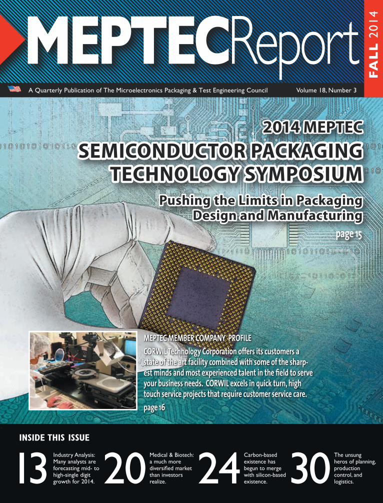
A Quarterly Publication of The Microelectronics Packaging & Test Engineering Council Volume 18, Number 3 - INSIDE THIS ISSUE 13 Industry Analysis: Many analysts are forecasting mid- to high-single digit growth for 2014. 24 Carbon-based existence has begun to merge with silicon-based existence. 30 The unsung heros of planning, production control, and logistics. MEPTEC MEMBER COMPANY PROFILE CORWIL Technology Corporation offers its customers a state of the art facility combined with some of the sharp- est minds and most experienced talent in the field to serve your business needs. CORWIL excels in quick turn, high touch service projects that require customer service care. page 16 FALL 2014 page 15 20 Medical & Biotech: a much more diversified market than investors realize. 2014 MEPTEC SEMICONDUCTOR PACKAGING TECHNOLOGY SYMPOSIUM Pushing the Limits in Packaging Design and Manufacturing
Transcript
A Quarterly Publication of The Microelectronics Packaging & Test Engineering Council Volume 18, Number 3
SPRING 2011 MEPTEC Report 3
-INSIDE THIS ISSUE
13 Industry Analysis: Many analysts are forecasting mid- to high-single digit growth for 2014. 24
Carbon-based existence has begun to merge with silicon-based existence. 30
The unsung heros of planning, production control, and logistics.
MEPTEC MEMBER COMPANY PROFILECORWIL Technology Corporation offers its customers a state of the art facility combined with some of the sharp-est minds and most experienced talent in the field to serve your business needs. CORWIL excels in quick turn, high touch service projects that require customer service care.page 16
FAL
L 2
014
page 15
20 Medical & Biotech: a much more diversified market than investors realize.
2014 MEPTEC
SEMICONDUCTOR PACKAGING TECHNOLOGY SYMPOSIUM
Pushing the Limits in Packaging Design and Manufacturing
MOST EVERYONE IN ELECTRONICS is familiar with Moore’s Law and some have even predicted its extinction or proclaimed it dead already. I contend, however, that if the industry continues on its path of smaller geometries with more speed and more function, Moore’s Law will maintain its dominance as a technolo-gy predictor. The “law”, developed by the infamous Intel co-founder for which the rule is named, dictates the doubling of the number of transistors on a chip every 24 months. Our company sees the advance of Moore’s Law on a daily basis – but with the added challenge of increasing I/O counts in higher and higher densities. The effects of Moore’s Law are having huge impacts on package designs, mate-rial requirements, process modifications and device capability. The higher transis-tor count results in increased lead density and finer pitches. One look at Intel’s prod-uct line alone paints a picture. The Intel 8008 processor debuted in 1979 and had and I/O of 40 leads with 40,000 transis-tors. By contrast and just six years later, the Intel 386 processor came in at a whop-ping 275,000 transistors with I/O of 140 leads. Today, it’s not uncommon for I/O to exceed 1000, with 5 Billion transistors. The push toward smaller form and greater function is also forcing changes in package design methodologies. Not too long ago, most high-performance devices such as QFPs, SiPs and QFNs relied exclusively on wirebonding techniques to form the device interconnections. With
less than 40 µm and the pitch densities are very high, it becomes increasingly more difficult to ensure complete flow and adequate coverage, which introduces the possibility of voids and limits the bump protection. As mentioned previously, to facilitate the demands for higher-functioning, min-iaturized devices, flip-chip designs are quickly moving away from larger solder bumps and toward new bump technolo-gies such as copper (Cu) pillar, which can adapt for ultra-fine pitches while offering the benefits of better electrical connec-tions and improved reliability. As the nar-row gaps with Cu pillar present challenges for traditional capillary underfills, many packaging specialists are turning to alter-natives. Advanced material solutions are moving away from capillary underfills, in favor of pre-applied processes like non-conductive paste (NCP) or even B-staged materials and films like wafer and sub-strate applied non-conductive underfill films (NCF) for applications where the lead density is too high for a capillary process. Materials like these will factor greatly in the advance of higher-density, more capable package designs and the assurance that Moore’s Law will maintain its relevance. So far, I’ve seen no signs of package capability decreasing. Materials advances and processes have also kept pace – and often surpassed – the progression of tech-nology. Long live Moore! ◆
this structure, die connectivity is achieved by routing thin wires from the top of the die to the pad interconnect on the substrate. Though still widely employed today, wirebonding is yielding some of its dominance to flip-chip processes. The move toward greater functionality in decreasing dimensions – not to men-tion the need for better performance and manufacturing flexibility – higher I/O counts, package integration and tighter bump pitches are dictating the use of flip-chip technology to advance new package designs. Flip-chip designs are numerous, with some incorporating gold stud bumps, stacked bumps, gold plated studs and, more recently, copper pillars with sol-der caps, which are quickly becoming the connection method of choice. These designs – particularly those with very tight pitches – also require a paradigm shift in materials. Unlike wirebonded packages, flip-chip packages use underfill for pro-tection of the interconnected bumps and these materials have had to adapt to cope with the Moore’s Law effect. Depending on the application and the bump density, a variety of different underfill materials can be used effectively for device protec-tion. In cases where the bump pitches are greater than 100 µm, traditional capillary underfills are highly capable. For narrow gap, fine-pitch devices, however, capillary underfills present challenges. Capillary action is driven by the gap and vacuum action within the gap. When the gap is
BOARD LETTER
Moore’s Law Lives OnDimension Decrease Drives New Package Designs, Materials Requirements Doug Dixon Henkel Electronic Materials, LLC
FALL 2014 MEPTEC REPORT 3meptec.org
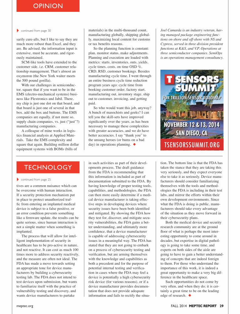
T SENSORS SUMMIT™
FOR TRILLION SENSOR ROADMAP
Estancia La Jolla Hotel & Spa, La Jolla, CANovember 12-13, 2014
R E G I S T E R O N L I N E T O D A Y A T W W W . T S E N S O R S S U M M I T . O R G
MEPTEC Report Vol. 18, No. 3. Published quarterly by MEPCOM LLC, P. O. Box 222, Medicine Park, OK 73557. Copyright 2014 by MEPTEC/MEPCOM LLC. All rights reserved. Materials may not be reproduced in whole or in part without written permission. MEPTEC Report is sent without charge to members of MEPTEC. For non-members, yearly subscriptions are available for $75 in the United States, $80US in Canada and Mexico, and $95US elsewhere. For advertising rates and information contact Gina Edwards at 408-858-5493, Fax Toll Free 1-866-424-0130.
A Quarterly Publication of The Microelectronics Packaging & Test Engineering Council Volume 18, Number 3
The MEPTEC Report is a Publication of the Microelectronics Packaging & Test
Engineering Council
P. O. Box 222, Medicine Park, OK 73557Tel: (650) 714-1570 Email: [email protected]
Publisher MEPCOM LLC
Editor Bette Cooper
Art Director/Designer Gary Brown
Sales Manager Gina Edwards
MEPTEC Advisory Board
Board Members
Ivor Barber Xilinx, Inc.
Jeanne Beacham Delphon Industries
Joel Camarda Semiops
Jeff Demmin STATS ChipPAC, Inc.
Douglass Dixon Henkel Corporation
Nikhil Kelkar Exar Corporation
Nick Leonardi Micross Components
Phil Marcoux PPM Associates
Bhavesh Muni Dow Chemical Corp.
Kumar Nagarajan Maxim Integrated
Raj Pendse STATS ChipPAC
Rich Rice ASE (US) Inc.
Jim Walker Gartner
John Xie Altera Corporation
Special Advisors
Ron Jones N-Able Group International
Mary Olsson Gary Smith EDA
Honorary Advisors
Seth Alavi Sunsil
Gary Catlin Plexus
Rob Cole
Skip Fehr
Anna Gualtieri Elle Technology
Marc Papageorge ICINTEK
In Memoriam
Bance Hom
Contributors
Mike Ahmadi, CISSP Codenomicon
Joel Camarda SemiOps
Doug Dixon Henkel Electronic Materials, LLC
Ira Feldman Feldman Engineering Corp.
Dan Fenner The Electronics Group of Henkel
Ron Jones N-Able Group International
Serafin Pedron Promex Industries
Chris Pugh Promex Industries
Dan Tracy SEMI
FALL
201
4
ON THE COVER2014 MEPTEC Semiconductor Packaging Technology Symposium – Pushing the Limits in Packaging Design and Manufacturing. Don’t miss your chance to get up to speed on today’s most important topics in packaging, all in one place on one day. The opportunity to learn is en-hanced with MEPTEC’s unmatched Silicon Valley networking opportuni-ties built into the day. Thursday, October 23rd at the Biltmore Hotel & Suites in Santa Clara, California.
13 ANALYSIS – For 2014 and 2015, the global economy is expected to improve and grow at rates above the
past few year, and, with that being the case, many analysts are forecasting mid- to high-single digit growth for the semicon-ductor revenues for 2014. Current projections for 2015 are likewise positive.
BY DAN TRACY, SEMI
20 ASSEMBLY – The ever shrinking size and mass of electronic components that enable new products is
as much a driver for the medical products industry as is the pursuit of more functions per IC chip area. New applica-tions in the medical area are both utilizing new IC packaging techniques and materials and driving even more innovation.
BY SERAFIN PEDRON AND CHRIS PUGH PROMEX INDUSTRIES
16 PROFILE – CORWIL Technology Corporation is the premier, US based, IC assembly and test services sub-
contractor. They offer full back-end assembly services start-ing from wafer sort, thinning & dicing through die-attach, wirebond, package sealing and final test. CORWIL has the experience to meet your most demanding challenges.
CORWIL TECHNOLOGY CORPORATION MEMBER COMPANY PROFILE
DEPARTMENTS 3 Board Letter 5 Member News
9 Industry Insights Column 10 Coupling & Crosstalk Column
26 Henkel News30 Opinion
Region 2014 Year-to-Date (June) 2013 Year-to-Date (June) Y/Y % Change
Europe $1,144 $733 56.0% Japan $1,972 $1,447 36.3% North America $4,120 $2,681 53.7% Korea $3,818 $2,078 83.8% Taiwan $5,063 $5,564 -9.0% China $2,752 $1,391 97.9% ROW $908 $957 -5.1%
Total $19,778 $14,851 33.2%
FALL 2014 MEPTEC REPORT 13meptec.org
ANALYSIS
2014 and 2015 Industry Outlook Dan Tracy, SEMI
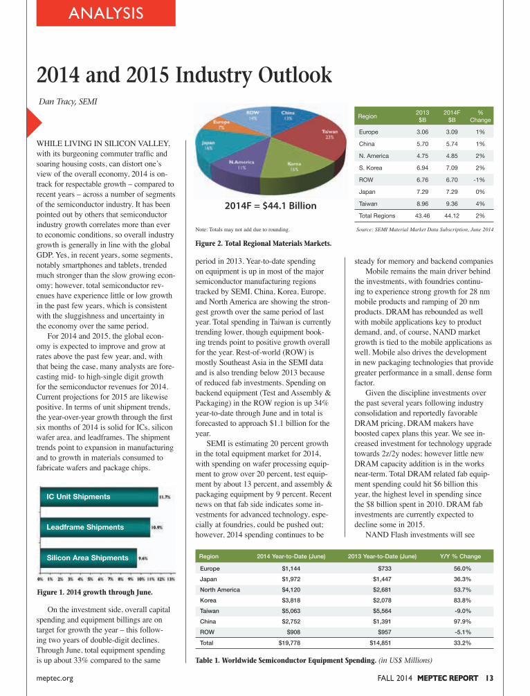
WHILE LIVING IN SILICON VALLEY, with its burgeoning commuter traffic and soaring housing costs, can distort one’s view of the overall economy, 2014 is on-track for respectable growth – compared to recent years – across a number of segments of the semiconductor industry. It has been pointed out by others that semiconductor industry growth correlates more than ever to economic conditions, so overall industry growth is generally in line with the global GDP. Yes, in recent years, some segments, notably smartphones and tablets, trended much stronger than the slow growing econ-omy; however, total semiconductor rev-enues have experience little or low growth in the past few years, which is consistent with the sluggishness and uncertainty in the economy over the same period. For 2014 and 2015, the global econ-omy is expected to improve and grow at rates above the past few year, and, with that being the case, many analysts are fore-casting mid- to high-single digit growth for the semiconductor revenues for 2014. Current projections for 2015 are likewise positive. In terms of unit shipment trends, the year-over-year growth through the first six months of 2014 is solid for ICs, silicon wafer area, and leadframes. The shipment trends point to expansion in manufacturing and to growth in materials consumed to fabricate wafers and package chips.
On the investment side, overall capital spending and equipment billings are on target for growth the year – this follow-ing two years of double-digit declines. Through June, total equipment spending is up about 33% compared to the same
period in 2013. Year-to-date spending on equipment is up in most of the major semiconductor manufacturing regions tracked by SEMI. China, Korea, Europe, and North America are showing the stron-gest growth over the same period of last year. Total spending in Taiwan is currently trending lower, though equipment book-ing trends point to positive growth overall for the year. Rest-of-world (ROW) is mostly Southeast Asia in the SEMI data and is also trending below 2013 because of reduced fab investments. Spending on backend equipment (Test and Assembly & Packaging) in the ROW region is up 34% year-to-date through June and in total is forecasted to approach $1.1 billion for the year. SEMI is estimating 20 percent growth in the total equipment market for 2014, with spending on wafer processing equip-ment to grow over 20 percent, test equip-ment by about 13 percent, and assembly & packaging equipment by 9 percent. Recent news on that fab side indicates some in-vestments for advanced technology, espe-cially at foundries, could be pushed out; however, 2014 spending continues to be
steady for memory and backend companies Mobile remains the main driver behind the investments, with foundries continu-ing to experience strong growth for 28 nm mobile products and ramping of 20 nm products. DRAM has rebounded as well with mobile applications key to product demand, and, of course, NAND market growth is tied to the mobile applications as well. Mobile also drives the development in new packaging technologies that provide greater performance in a small, dense form factor. Given the discipline investments over the past several years following industry consolidation and reportedly favorable DRAM pricing, DRAM makers have boosted capex plans this year. We see in-creased investment for technology upgrade towards 2z/2y nodes; however little new DRAM capacity addition is in the works near-term. Total DRAM related fab equip-ment spending could hit $6 billion this year, the highest level in spending since the $8 billion spent in 2010. DRAM fab investments are currently expected to decline some in 2015. NAND Flash investments will see
Figure 1. 2014 growth through June.
IC Unit Shipments
Silicon Area Shipments
Leadframe Shipments
Figure 2. Total Regional Materials Markets.
Source: SEMI Material Market Data Subscription, June 2014Note: Totals may not add due to rounding.
2014F = $44.1 Billion
Region 2013 2014F % $B $B Change
Europe 3.06 3.09 1%
China 5.70 5.74 1%
N. America 4.75 4.85 2%
S. Korea 6.94 7.09 2%
ROW 6.76 6.70 -1%
Japan 7.29 7.29 0%
Taiwan 8.96 9.36 4%
Total Regions 43.46 44.12 2%
Table 1. Worldwide Semiconductor Equipment Spending. (in US$ Millions)
FALL 2014 MEPTEC REPORT 25meptec.org24 MEPTEC REPORT FALL 2014 meptec.org
TECHNOLOGY
I BELIEVE THAT MODERN MEDICAL research balances healing with what caused the need for healing in the first place. In ancient times, some causes were obvious, such as a laceration pre-cipitating the need for sutures. Other causes were not so obvious, such as a fever brought on by bacterial infection. Early healers often attributed fevers to “bad blood” or “demons”, and either performed barbaric rituals such as blood letting, or brought in high priests to perform religious rituals. It was not until scientists, such as Louis Pasteur, discovered the world of bacterial organ-isms when we began a field of study that provided us truly useful information about the world of what we now know as pathogens. It is my understanding that this work by Pasteur and others before and after that was both extremely controversial, and extremely beneficial. For someone to suggest that a doctor should wash his hands prior to performing a procedure was considered absolutely ludicrous. Those who suggested this would solve many of the problems caused by what we know as pathogens today were often shunned, and ridiculed. I am happy to see that the medical community came around, and eventually adopted hygienic practices. I believe this led to fields of study focused on micro-organisms, and all pathogens in general. I also believe this led to forensic pathol-ogy, where medical professionals could work to determine the cause of damage or death of a patient through working back from the outcome. Since the onset of the study of patho-gens, the focus has always been on car-bon-based pathogens and their effect on carbon-based life forms. This certainly would seem adequate, since humans are carbon-based life forms. However, mod-ern medicine has led us down a pathway were we need to revisit this notion, and
The Age Of The Digital Pathogen Mike Ahmadi, CISSP Global Director, Business Development Codenomicon
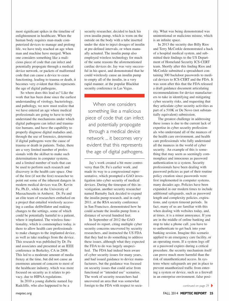
most significant spikes in the timeline of enlightenment in healthcare. When the human body requires man-made com-puterized devices to manage and prolong life, we have truly reached an age when man and machine have merged. When one considers something like a mali-cious piece of code that can infect and potentially propogate through a medical device network, or packets of malformed code that can cause a device to cease functioning, leading to trauma or death, it becomes very evident that this represents the age of digital pathogens. So where does this lead us? Like the work that has been done since the earliest understanding of virology, bacteriology, and pathology, we now must realize that we have entered an age where medical professionals are going to have to truly understand the mechanisms under which digital pathogens can infect and trauma-tize humans, and have the capability to properly diagnose digital maladies and, through the use of forensics, determine if digital pathogens were the cause of trauma or death in patients. Today, there are a very limited number of profes-sionals with the skillset to make such determinations in computer systems, and a limited number of tools that can be used to perform such research and discovery in the health care space. One of the first (if not the first) researcher to point out some of the inherent dangers in modern medical devices was Dr. Kevin Fu, Ph.D., while at the University of Massachusetts in Amherst. Dr. Fu and an elite team of researchers embarked on a project that entailed wirelessly access-ing a cardiac defibrillator and making changes to the settings, some of which could be potentially harmful to a patient, where it implanted. The wireless func-tionality, which is commonplace today, is there to allow health care professionals to make changes to the implanted device, as well as take readings from the device. This research was published by Dr. Fu and associates and presented at an IEEE conference in Berkeley, CA in 2008. This led to a moderate amount of media frenzy at the time, but did not cause an enormous amount of concern to most of the healthcare industry, which was more focused on security as it relates to pri-vacy, due to HIPAA regulations. In 2010 a young diabetic named Jay Radcliffe, who also happened to be a
security researcher, decided to hack his own insulin pump, which is worn on the outside on the body with a tube inserted under the skin to inject dosages of insulin at pre-defined intervals, or when manu-ally actuated. The insulin pump also employed wireless technology for much of the same reasons the aforementioned cardiac devices do. Jay was very success-ful in his quest, and demonstrated that he could wirelessly cause an insulin pump to empty all of the insulin, in a very rapid manner, at the popular Blackhat security conference in Las Vegas.
Jay’s work created a bit more contro-versy than Dr. Fu’s earlier work, and made its way to a congressional repre-sentative, which prompted a GAO inves-tigation into cyber security of medical devices. During the timespan of this in-vestigation, another security researcher named Barnaby Jack decided to expand the insulin pump research, and in early 2011, at the RSA security conference in San Francisco, demonstrated how he could actuate the insulin pump from a distance of several hundred feet. In September of 2012 the GAO released its report, citing multiple cyber security concerns uncovered by security researchers, and instructed the US FDA that they had to do something to address these issues, although what they expected the FDA to do was largely unspeci-fied. The FDA had indeed been aware of cyber security issues for many years, and had issued guidance to device manu-facturers, but the guidance was focused on security issues that could arise from functional or “intended use” scenarios. The work of security researchers had uncovered an area that was somewhat foreign to the FDA with respect to secu-
rity. What was being demonstrated was unintentional or malicious misuse, which is an infinite space. In 2013 the security duo Billy Rios and Terry McCorkle demonstrated a hack of a hospital medical system, and sub-mitted their findings to the US Depart-ment of Homeland Security ICS-CERT team. Shortly after this finding Rios and McCorkle submitted a spreadsheet con-taining 300 backdoor passwords to medi-cal devices to ICS-CERT and the FDA. It was soon after this that the FDA released a draft guidance document articulating recommendations for device manufactur-ers to take in identifying and mitigating cyber security risks, and requesting that they articulate cyber security activities as part of a 510K or De Novo (not substan-tially equivalent) submission. The greatest challenge in addressing these issues is due to the current lack of expertise in cyber security profession-als who understand all of the nuances of the health care environment, and health care professionals who fully understand all the nuances in the world of cyber security. An example of this is some-thing that may seem as seemingly com-monplace and innocuous as password authentication to a system. Security professionals have been dealing with password policies as part of their routine policy creation since passwords were first implemented in computer systems, many decades ago. Policies have been expanded in our modern times to include additional safeguards, such as password length and complexity policies, expira-tions, and system timeout periods. In fact, many of us are familiar with this when dealing with websites today, and, at times, it is a minor annoyance. If you are in the middle of online banking and stop to take a phone call, you have to re-authenticate to get back into your banking session. Imagine this scenario applied to an emergency care facility, or an operating room. If a system logs off or a password expires during a critical procedure, the security mechanism itself can prove much more harmful than the risk of unauthenticated access. In sys-tems where safeguards are put in place to prevent unauthorized traffic from enter-ing a system or device, such as a firewall in an enterprise environment, false posi-
When one considers something like a malicious
piece of code that can infect and potentially propogate through a medical device
network ... it becomes very evident that this represents the age of digital pathogens.
perhaps expand our under-standing of pathogens. As previously mentioned, the advent of computerized medical devices and technologies has led to enormous health benefits. Pacemakers, insulin pumps, and more can be implanted in or on patients to serve as a way to augment the func-tionality of vital organs. Patients in criti-cal care environments are tethered to life support systems, and various other devic-es that intelligently monitor and control vital body systems. In the blink of an eye, carbon-based (human) existence has begun to merge with silicon-based (com-puter) existence. In my viewpoint, the intelligent com-puterized medical device has become the equivalent of a vital organ. If a device is required to maintain life functions, it is vital, and a failure in such devices can lead to severe trauma, or death. Failures can occur in such devices, and sometimes do occur for various reasons. Sometimes it is a design flaw that mani-fests itself over time, other times it is through lack of proper care, use, or main-tenance. However, a new category of failure scenarios has emerged, and these are induced by vulnerabilities in the code and communication protocols operating on these devices, which can lead to unin-tended and previously unknown failure modes. Sometimes the vulnerabilities are intended features that are exploited by
either curious or mali- cious actors. An example would be an implanted pacemaker that reveals a serial number when queried, allowing a would-be attacker to gain access to a specific device for potentially nefarious purposes, or to potentially inject mali-cious code into the device. Other devices can be forced to cease functioning as intended, either temporarily or perma-nently, by bombarding the device with malformed digital traffic. This type of vulnerability is discovered through a pro-cess known as fuzz testing or “fuzzing”, where a software program methodically steps through multiple permutations of malformed code in order to induce such failures, for the purpose of discovering previously unknown vulnerabilities. In 2013 the US Food and Drug Administra-tion decided this type of tool would be of great benefit to their newly formed cybersecurity testing lab, and of great benefit to device manufacturers for their own internal testing process, prior to submission to the FDA for 510K or new submissions. The FDA acquired a tool known as Codenomicon Defensics, and began recommending that device manu-facturers include fuzz testing as one of several means of discovering cybersecu-rity related vulnerabilities. This now leads to what I would consider one of the newest, and perhaps continued on page 24
A Quarterly Publication of The Microelectronics Packaging & Test Engineering Council Volume 18, Number 3
SPRING 2011 MEPTEC Report 3
-INSIDE THIS ISSUE
13 Industry Analysis: Many analyists are forecasting mid- to high-single digit growth for 2014. 24
Carbon-based existence has begun to merge with silicon-based existence. 30
The unsung heros of planning, production control, and logistics.
MEPTEC MEMBER COMPANY PROFILECORWIL Technology Corporation offers its customers a state of the art facility combined with some of the sharp-est minds and most experienced talent in the field to serve your business needs. CORWIL excels in quick turn, high touch service projects that require customer service care.page 16
FAL
L 2
014
page 15
20 Medical & Biotech: a much more diversified market than investors realize.
2014 MEPTEC
SEMICONDUCTOR PACKAGING TECHNOLOGY SYMPOSIUM
Pushing the Limits in Packaging Design and Manufacturing
PROFILE
16 MEPTEC REPORT FALL 2014 meptec.org FALL 2014 MEPTEC REPORT 17meptec.org
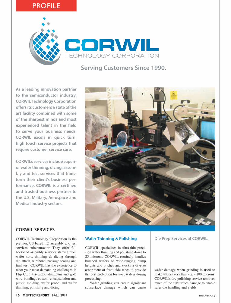
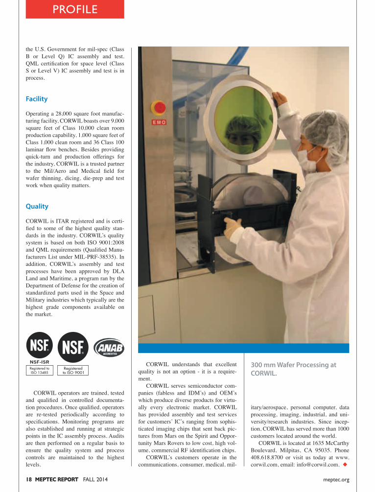
Wafer Thinning & Polishing
CORWIL specializes in ultra-thin preci-sion wafer thinning and polishing down to 25 microns. CORWIL routinely handles bumped wafers of wide-ranging bump heights and pitches and stocks a diverse assortment of front side tapes to provide the best protection for your wafers during processing. Wafer grinding can create significantsubsurface damage which can cause
wafer damage when grinding is used to make wafers very thin, e.g. <100 microns. CORWIL’s dry polishing service removes much of the subsurface damage to enable safer die handling and yields.
CORWIL SERVICES
CORWIL Technology Corporation is the premier, US based, IC assembly and test services subcontractor. They offer full back-end assembly services starting from wafer sort, thinning & dicing through die-attach, wirebond, package sealing and finaltest.CORWILhastheexperiencetomeet your most demanding challenges in Flip Chip assembly, aluminum and gold wire bonding, custom encapsulation and plastic molding, wafer probe, and wafer thinning, polishing and dicing.
resulting in greater market share and increased profitability for their custom-ers. CORWIL is the sole source provider of prototyping services in Flip Chip and wire bonded BGA’s for many fabless companies as well as full IDMs (Inte-grated Device Manufacturers with wafer fabs)andOEM’swithapplicationspecificdevices. CORWIL also is the designated provider for pre-production quantities, overflowproduction,andforend-of-quar-ter or end-of-year production surges for many customers.
Volume Production
CORWIL is the highest volume subcon-tractor of wafer dicing, visual inspection, and die pick & place services in the US,
producing tens of millions of die per month for its customers. For commercial markets, such as communications, imag-ing, PC, and consumer/industrial, COR-WIL’s IC assembly and test production capabilities range from plastic packages such as QFN’s, to complex BGA’s andmulti-chip-modules. Additionally, for the mil/aero markets, CORWIL assembles and tests IC’s in ceramic packages includ-ingfullmil-specprocessflowsandenvi-ronmentalscreening.CORWILiscertifiedQML (Qualified Manufacturers List) by
Test Division
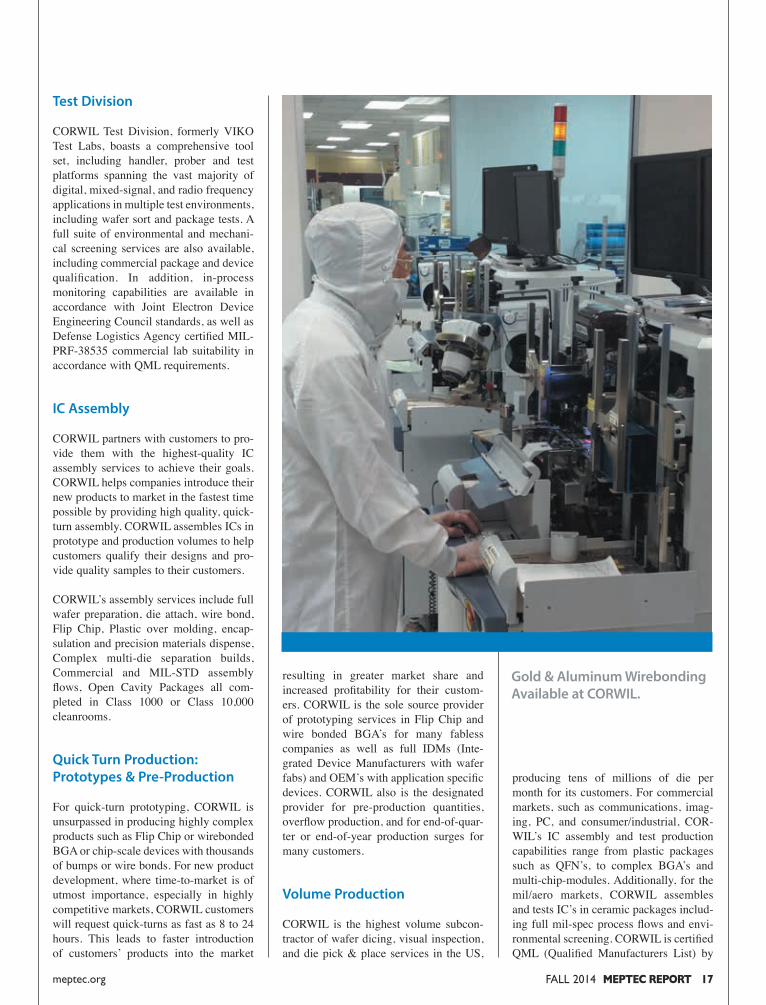
CORWIL Test Division, formerly VIKO Test Labs, boasts a comprehensive tool set, including handler, prober and test platforms spanning the vast majority of digital,mixed-signal,andradiofrequencyapplications in multiple test environments, including wafer sort and package tests. A full suite of environmental and mechani-cal screening services are also available, including commercial package and device qualification. In addition, in-processmonitoring capabilities are available in accordance with Joint Electron Device Engineering Council standards, as well as DefenseLogisticsAgencycertifiedMIL-PRF-38535 commercial lab suitability in accordance with QML requirements.
IC Assembly
CORWIL partners with customers to pro-vide them with the highest-quality IC assembly services to achieve their goals. CORWIL helps companies introduce their new products to market in the fastest time possible by providing high quality, quick-turn assembly. CORWIL assembles ICs in prototype and production volumes to help customers qualify their designs and pro-vide quality samples to their customers.
CORWIL’s assembly services include full wafer preparation, die attach, wire bond, Flip Chip, Plastic over molding, encap-sulation and precision materials dispense, Complex multi-die separation builds,Commercial and MIL-STD assembly flows, Open Cavity Packages all com-pleted in Class 1000 or Class 10,000 cleanrooms.
For quick-turn prototyping, CORWIL is unsurpassedinproducinghighlycomplexproducts such as Flip Chip or wirebonded BGA or chip-scale devices with thousands of bumps or wire bonds. For new product development, where time-to-market is of utmost importance, especially in highly competitive markets, CORWIL customers will request quick-turns as fast as 8 to 24 hours. This leads to faster introduction of customers’ products into the market
As a leading innovation partner to the semiconductor industry, CORWIL Technology Corporation offers its customers a state of the art facility combined with some of the sharpest minds and most experienced talent in the field to serve your business needs. CORWIL excels in quick turn, high touch service projects that require customer service care.
CORWIL’s services include superi-or wafer thinning, dicing, assem-bly and test services that trans-form their client’s business per-formance. CORWIL is a certified and trusted business partner to the U.S. Military, Aerospace and Medical industry sectors.
WAFER THINNING & POLISHING
IC ASSEMBLY
Die Prep Services at CORWIL.
Serving Customers Since 1990.
Gold & Aluminum Wirebonding Available at CORWIL.
24 TECHNOLOGY – The Age of the Digital Pathogen: The advent of computerized medical devices and tech-
nologies has led to enormous health benefits. In the blink of an eye, carbon-based (human) existence has begun to merge with silicon-based (computer) existence.
BY MIKE AHMADI, CISSP CODENOMICON
Medical & Biotech Electronic Assembly Presents Many Challenges
tronic devices are intended for personal use but since there is a chance of their use as a medical diagnostic, it behooves any manufacturer to be aware of the FDA regulations. The US FDA recently released a guidance for some types of medical device qualification entitled “Medical Device Development Tools, Draft Guid-ance for Industry, Tool Developers, and Food and Drug Administration Staff”, issued November 14, 2013. As stated below the intent of this guidance is to streamline the steps needed by a device maker to develop and qualify a product for the market.
a prelude to completing the Operational Qualification, or OQ. The Installation Qualification (IQ) is generally straightforward and is simply documenting that the equipment has been installed and is performing per the equip-ment manufacturer’s requirements. Mandatory quality procedures include IQ for Installation Qualification, OQ for Operational Qualification and PQ for Process Qualification.
What Regulatory Agencies Govern the Production of These Devices? The common belief is that the US Food and Drug Administration, or FDA is the sole regulatory agency for medi-cal devices. This is true if the product is intended to provide a source of data, such as a BioMarker from which a medical analysis and diagnosis might be based. Many of the new wearable elec-
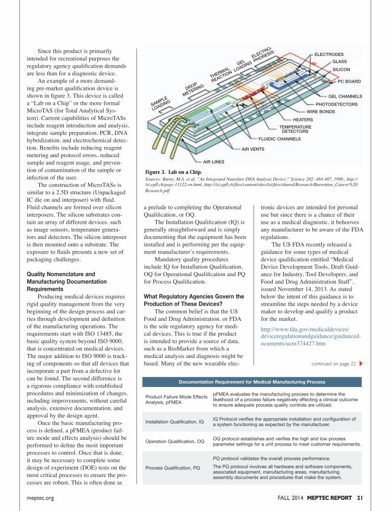
Since this product is primarily intended for recreational purposes the regulatory agency qualification demands are less than for a diagnostic device. An example of a more demand-ing pre-market qualification device is shown in figure 3. This device is called a “Lab on a Chip” or the more formal MicroTAS (for Total Analytical Sys-tem). Current capabilities of MicroTASs include reagent introduction and analysis, integrate sample preparation, PCR, DNA hybridization, and electrochemical detec-tion. Benefits include reducing reagent metering and protocol errors, reduced sample and reagent usage, and preven-tion of contamination of the sample or infection of the user. The construction of MicroTASs is similar to a 2.5D structure (Unpackaged IC die on and interposer) with fluid. Fluid channels are formed over silicon interposers. The silicon substrates con-tain an array of different devices, such as image sensors, temperature genera-tors and detectors. The silicon interposer is then mounted onto a substrate. The exposure to fluids presents a new set of packaging challenges.
Quality Nomenclature and Manufacturing Documentation Requirements Producing medical devices requires rigid quality management from the very beginning of the design process and car-ries through development and definition of the manufacturing operations. The requirements start with ISO 13485, the basic quality system beyond ISO 9000, that is concentrated on medical devices. The major addition to ISO 9000 is track-ing of components so that all devices that incorporate a part from a defective lot can be found. The second difference is a rigorous compliance with established procedures and minimization of changes, including improvements, without careful analysis, extensive documentation, and approval by the design agent. Once the basic manufacturing pro-cess is defined, a pFMEA (product fail-ure mode and effects analysis) should be performed to define the most important processes to control. Once that is done, it may be necessary to complete some design of experiment (DOE) tests on the most critical processes to ensure the pro-cesses are robust. This is often done as
ASSEMBLY
The teardown of the wearable device of figure 2 shows a rigid-flex substrate enabling a “cordwood” type of assembly. The array of components assembled to the substrate consists of wire bonded bare ICs and reflow soldered passive and IC components. As expected the largest unit component in the device is the bat-tery.
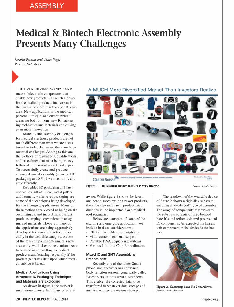
aware. While figure 1 shows the latest and hence, more exciting newer products, there are also many new product intro-ductions in the implantable and medical tool segments. Below are examples of some of the exciting and emerging applications we include in these considerations: • EKG connectable to Smartphones• Multi-camera head endoscopes• Portable DNA Sequencing systems• Various Lab-on-a-Chip Embodiments
Mixed IC and SMT Assembly is Predominant Recently one of the larger Smart-phone manufacturers has combined body function sensors, generically called BioMakers, into its wrist sized phone. This enables the collected data to be transferred to whatever data storage and analysis entities the wearer choses.
THE EVER SHRINKING SIZE AND mass of electronic components that enable new products is as much a driver for the medical products industry as is the pursuit of more functions per IC chip area. New applications in the medical, personal lifestyle, and entertainment areas are both utilizing new IC packag-ing techniques and materials and driving even more innovation. Basically the assembly challenges for medical electronic products are not much different than what we are accus-tomed to today. However, there are huge material challenges. Adding to this are the plethora of regulations, qualifications, and procedures that must be rigorously followed and present added challenges. To successfully create and produce advanced mixed assembly (advanced IC packaging and SMT) we must think and act differently. Embedded IC packaging and inter-connection, ultrathin die, metal pillars and hermetic wafer level packaging are some of the techniques being developed for the emerging applications. Many of these methods are viewed as being on the outer fringes, and indeed most current products employ conventional packag-ing and materials. However, many of the applications are being aggressively developed for mass production, espe-cially in the wearable category. As one of the few companies entering this new area early, we find extreme caution needs to be used in committing to medical product manufacturing, especially if the product generates data upon which medi-cal advice is based.
Medical Applications Using Advanced IC Packaging Techniques and Materials are Exploding As shown in figure 1 the market is much more diverse than many of us are
Serafin Pedron and Chris PughPromex Industries
20 MEPTEC REPORT FALL 2014 meptec.org FALL 2014 MEPTEC REPORT 21meptec.org
Figure 2. Samsung Gear Fit 2 teardown. Source: www.ifixit.com
Figure 1. The Medical Device market is very diverse. Source: Credit Suisse
A MUCH More Diversified Market Than Investors Realize
Documentation Requirement for Medical Manufacturing Process
Installation Qualification, IQ IQ Protocol verifies the appropriate installation and configuration of a system functioning as expected by the manufacturer.
Product Failure Mode Effects Analysis, pFMEA
pFMEA evaluates the manufacturing process to determine the likelihood of a process failure negatively effecting a clinical outcome to ensure adequate process quality controls are utilized.
Operation Qualification, OQ OQ protocol establishes and verifies the high and low process parameter settings for a unit process to meet customer requirements.
Process Qualification, PQ
PQ protocol validates the overall process performance. The PQ protocol involves all hardware and software components, associated equipment, manufacturing areas, manufacturing assembly documents and procedures that make the system.
continued on page 24
Figure 3. Lab on a Chip. Sources: Burns, M.A. et al. “An Integrated Nanoliter DNA Analysis Device,” Science 282: 484-487, 1998., http://lsi.epfl.ch/page-13122-en.html, http://lsi.epfl.ch/files/content/sites/lsi/files/shared/Research/Barrettino_Cancer%20Research.pdf
ELECTRODES
PC BOARD
SILICON
GLASS
GEL CHANNELS
HEATERS
WIRE BONDS
PHOTODETECTORS
TEMPERATURE DETECTORS
AIR LINES
AIR VENTS
FLUIDIC CHANNELS
SAMPLE
LOADING
ELECTRO-
PHORESIS
GEL
LOADING
THERMAL
REACTION
DROP
METERING
FALL 2014 MEPTEC REPORT 5meptec.org
The Fab Owners Association (FOA), a not for profit group of 26 semiconductor device manufacturers and nearly 60 industry suppliers, has opened membership to a select group of companies in the packag-ing, assembly and test seg-ment of integrated circuit manufacturing. Founded in 2004, the FOA has been bringing together device makers and their sup-pliers to cooperate on inno-vative solutions to compete efficiently on a global scale. As the complexity of packag-ing technology evolves to rival that of front-end device manufacturing, the FOA sees a need for packaging and test providers to also cooperate for efficiency and is opening membership to them in a new segment FOA-PT. Benefits of FOA-PT
membership include:• Meetings between FOA device makers and FOA-PT members to discuss common manufacturing and industry issues as well as meetings with Associate Members (suppliers to the industry).• Other networking and sponsorship opportunities throughout the year.• Access to short-term and annual member surveys to gauge issues and solutions that will include inputs from device makers as well as packaging and test members.• Free participation in the FOA’s “SpeedNetworking” event held annually in July at SEMICON West in San Fran-cisco, with impactful one-on-one meetings with FOA device makers.• Free participation in the FOA’s annual Collaborative
Forum in February. FOA-PT members will get the oppor-tunity to present case studies directly to FOA members, highlighting joint successes with device makers.• Free participation in the FOA’s Group Buying pro-grams (FOA Purchasing Partners, Inc.) “We recognize the impor-tance of packaging and test to the success of our industry and are excited to create an FOA segment focused on these areas,” commented L.T. Guttadauro, FOA Founder and Executive Director. “We have limited openings for charter members in FOA-PT who will also assist in setting the agenda for this new seg-ment.” For further information visit the FOA website at www.waferfabs.org. ◆
MEMBER NEWS
DAVID WATSON APPOINTED TO AMKOR BOARD OFDIRECTORSAmkor Technology, Inc. has appointed David
Watson as a new member
of the Company’s Board
of Directors. With this
appointment, Amkor’s
Board has been expanded
to nine members. Mr. Wat-
son is currently serving as
Executive Vice President
and Chief Operating Offi-
cer for Comcast Cable.
In this role Mr. Watson
oversees the teams re-
sponsible for day-to-day
operations of the cable
division, including sales
and marketing of cable
video, high-speed Internet
and voice services, as
well as oversight of the
three operating divisions
and Comcast Spotlight,
the advertising sales unit.
Before joining Comcast
Cable in 1991, he served
for seven years with Com-
cast Cellular Communica-
tions, Inc., first as Senior
Vice President of sales
and marketing and later as
President. Previously, he
headed sales and market-
ing efforts at Bell Atlantic
Mobile and Metrophone.
www.amkor.com
KULICKE & SOFFA APPOINTS DENNIS ANG LIEN LEE AS SENIOR DIRECTOR, GLOBAL HEAD OF IT Kulicke and Soffa Indus-tries, Inc. has announced
that the Company appoint-
ed Dennis Ang Lien Lee
as Senior Director, Global
Head of IT, effective imme-
diately. Mr. Ang will be
based at the K&S Corpo-
rate Headquarters in Sin-
Fab Owners Association Expands Membership to Include Packaging and Test
STATS CHIPPAC LTD. HAS ANNOUNCED that it has shipped over 100 million semicon-ductor packages with the Company’s fcCuBE® technology, advanced flip chip packaging with fine pitch copper (Cu) column bumps, Bond-on-Lead (BOL) interconnection and enhanced assembly processes. fcCuBE® technology is well established in the mobile market with the most significant production volume to date in small chip scale packages where the performance, size and cost benefits successfully address customer require-ments in smartphones, tablets and wearable devices. The compelling performance and cost advantages of fcCuBE are also accelerating the diversification of this advanced technology into large die packages for consumer and network-ing applications where very high performance, reliability and processing speeds are impera-tive. In consumer applications such as set top boxes (STB) and digital television (DTV) ICs, higher functionality, faster data rates and increased bandwidth are required for enhanced
user interfaces, rich graphics and outstand-ing audio quality. Wire bonding technology, a popular packaging choice in the past, is often unable to successfully address the increased thermal and electrical performance require-ments for next generation consumer applica-tions and, as a result, semiconductor companies are turning to high performance flip chip interconnect to differentiate their products. The BOL interconnection and very fine pitch Cu bumps in fcCuBE technology deliver excep-tionally high I/O density and bandwidth with excellent electromigration (EM) performance for high current carrying applications such as STB and DTV ICs at a cost competitive price point for customers. The functional and performance require-ments for networking devices continue to evolve as well, driving demand for larger and thinner packages supporting very high current densities and bandwidth requirements. For more information and details about STATS ChipPAC products and services visit www.statschippac.com. ◆
STATS ChipPAC’s fcCuBE® Technology Surpasses 100 Million Unit MilestoneReflects strong adoption in mobile applications with accelerated diversification in consumer and networking markets
6 MEPTEC REPORT FALL 2014 meptec.org
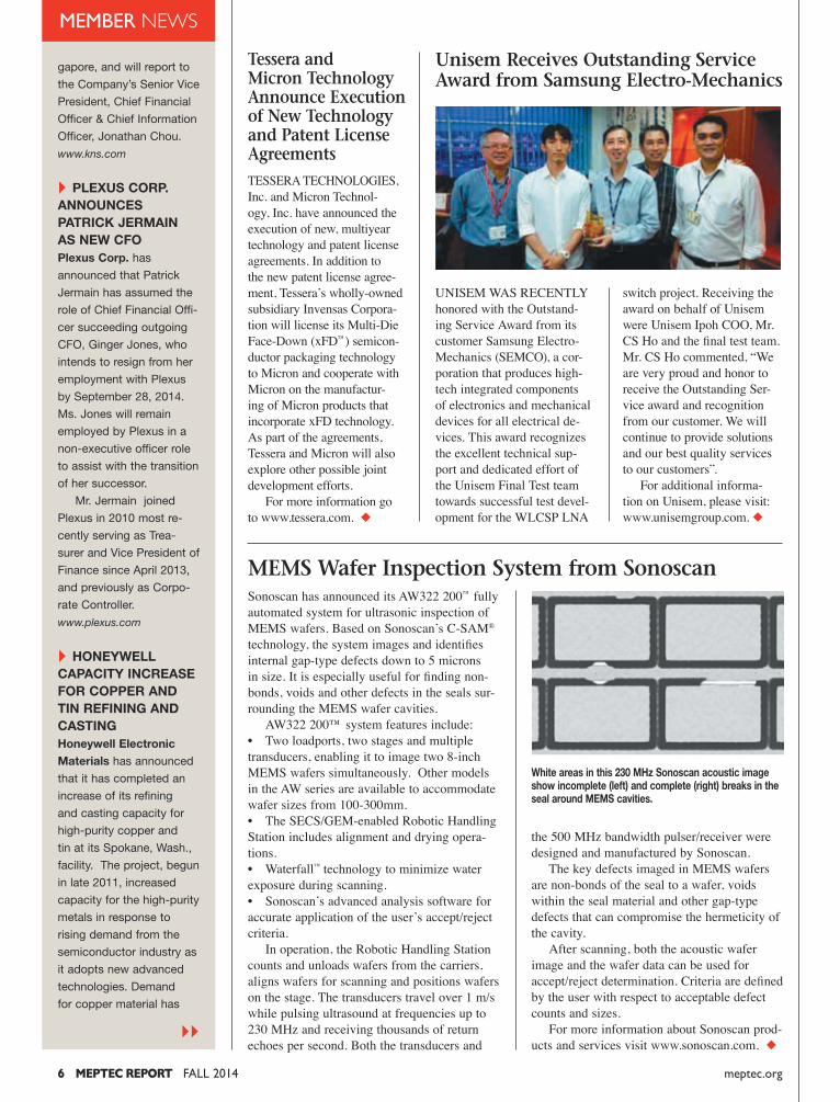
Unisem Receives Outstanding Service Award from Samsung Electro-Mechanics
UNISEM WAS RECENTLY honored with the Outstand-ing Service Award from its customer Samsung Electro-Mechanics (SEMCO), a cor-poration that produces high-tech integrated components of electronics and mechanical devices for all electrical de-vices. This award recognizes the excellent technical sup-port and dedicated effort of the Unisem Final Test team towards successful test devel-opment for the WLCSP LNA
switch project. Receiving the award on behalf of Unisem were Unisem Ipoh COO, Mr. CS Ho and the final test team. Mr. CS Ho commented, “We are very proud and honor to receive the Outstanding Ser-vice award and recognition from our customer. We will continue to provide solutions and our best quality services to our customers”. For additional informa-tion on Unisem, please visit: www.unisemgroup.com. ◆
MEMBER NEWS
gapore, and will report to
the Company’s Senior Vice
President, Chief Financial
Officer & Chief Information
Officer, Jonathan Chou.
www.kns.com
PLEXUS CORP. ANNOUNCES PATRICK JERMAIN AS NEW CFOPlexus Corp. has
announced that Patrick
Jermain has assumed the
role of Chief Financial Offi-
cer succeeding outgoing
CFO, Ginger Jones, who
intends to resign from her
employment with Plexus
by September 28, 2014.
Ms. Jones will remain
employed by Plexus in a
non-executive officer role
to assist with the transition
of her successor.
Mr. Jermain joined
Plexus in 2010 most re-
cently serving as Trea-
surer and Vice President of
Finance since April 2013,
and previously as Corpo-
rate Controller.
www.plexus.com
HONEYWELL CAPACITY INCREASE FOR COPPER AND TIN REFINING AND CASTINGHoneywell Electronic Materials has announced
that it has completed an
increase of its refining
and casting capacity for
high-purity copper and
tin at its Spokane, Wash.,
facility. The project, begun
in late 2011, increased
capacity for the high-purity
metals in response to
rising demand from the
semiconductor industry as
it adopts new advanced
technologies. Demand
for copper material has
Tessera and Micron Technology Announce Execution of New Technology and Patent License Agreements
Sonoscan has announced its AW322 200™ fully automated system for ultrasonic inspection of MEMS wafers. Based on Sonoscan’s C-SAM®
technology, the system images and identifies internal gap-type defects down to 5 microns in size. It is especially useful for finding non-bonds, voids and other defects in the seals sur-rounding the MEMS wafer cavities. AW322 200™ system features include:• Two loadports, two stages and multiple transducers, enabling it to image two 8-inch MEMS wafers simultaneously. Other models in the AW series are available to accommodate wafer sizes from 100-300mm.• The SECS/GEM-enabled Robotic Handling Station includes alignment and drying opera-tions.• Waterfall™ technology to minimize water exposure during scanning.• Sonoscan’s advanced analysis software for accurate application of the user’s accept/reject criteria. In operation, the Robotic Handling Station counts and unloads wafers from the carriers, aligns wafers for scanning and positions wafers on the stage. The transducers travel over 1 m/s while pulsing ultrasound at frequencies up to 230 MHz and receiving thousands of return echoes per second. Both the transducers and
the 500 MHz bandwidth pulser/receiver were designed and manufactured by Sonoscan. The key defects imaged in MEMS wafers are non-bonds of the seal to a wafer, voids within the seal material and other gap-type defects that can compromise the hermeticity of the cavity. After scanning, both the acoustic wafer image and the wafer data can be used for accept/reject determination. Criteria are defined by the user with respect to acceptable defect counts and sizes. For more information about Sonoscan prod-ucts and services visit www.sonoscan.com. ◆
MEMS Wafer Inspection System from Sonoscan
White areas in this 230 MHz Sonoscan acoustic image show incomplete (left) and complete (right) breaks in the seal around MEMS cavities.
TESSERA TECHNOLOGIES, Inc. and Micron Technol-ogy, Inc. have announced the execution of new, multiyear technology and patent license agreements. In addition to the new patent license agree-ment, Tessera’s wholly-owned subsidiary Invensas Corpora-tion will license its Multi-Die Face-Down (xFD™) semicon-ductor packaging technology to Micron and cooperate with Micron on the manufactur-ing of Micron products that incorporate xFD technology. As part of the agreements, Tessera and Micron will also explore other possible joint development efforts. For more information go to www.tessera.com. ◆
FALL 2014 MEPTEC REPORT 7meptec.org
New Ownership at F&K DelvotecON 24 JULY 2014, STRAMA-MPS Maschinenbau GmbH & Co. KG located in Straub-ing, Bavaria, took possession of 51% of the company’s shares from owner and presi-dent Dr. Farhad Farassat. It was also agreed that Dr. Far-assat will remain active in thecompany for another three years before the remaining shares will change hands.Strama-MPS (www.strama-mps.de) has very successfully carved a position for itselfas a specialty equipment sup-plier in the automotive, elec-trical and solar technologyindustries. Joining forces will create considerable synergies for both companies, notonly on the market side but also on the sourcing side. Strama-MPS has been verysuccessful in providing large and complex automation solu-tions for various industrysegments, especially in the highly demanding automo-tive industry. Thanks to their inhouse production facilities which include plants in lower-cost countries such as Croatia and China, they enjoy a large degree of vertical integra-tion. F&K Delvotec, on the other hand, provides highly regarded and leading-edge technologies in wirebonding. Dr. Farassat comments on the transaction: “The decid-ing factor to join forces with Strama-MPS was that both
our companies share the same philosophy. Strama-MPS with about 800 employees world-wide is a typical, family-owned Mittelstand company and yet is large enough to have the standing and the resources to compete success-fully in global growth mar-kets. I am happy to know that the future of the entire F&K Delvotec family which Said Kazemi and I built over 37 years into a highly esteemed technology leader will be in capable hands. All of us here at F&K Delvotec are grateful for the many years of fruitful and pleasurable cooperation with our customers that we have enjoyed. This will, I am confident, not change in the future.” As detailed by Dr. Farassat, F&K Delvotec will keep the company seat, R&D and production as well as sales and service departments and all employees at the company seat in Ottobrunn. Likewise, the locations and employees of our sales andservice subsidiaries in Sin-gapore and Foothill Ranch, California, will remain unchanged. In the coming years, we look forward to bring fresh vigor to larger, more complex and more highly automated projects from a single source to world-wide customers and help them stay ahead in their respective industries. ◆
847-437-6400 • sonoscan.com
Elk Grove Village, IL • Silicon Valley, CA • Phoenix, AZ • EnglandPhilippines • Singapore • Shanghai • Taiwan
847-437-6400 • sonoscan.com
An ISO/IEC 17025:2005 Certifi ed Testing Lab* SonoLab, a division of Sonoscan®, is the world’s largest inspection service specializing in Acoustic Micro Imaging (AMI). Through SonoLab, you’ll have access to the superior image quality and reliable data accuracy of Sonoscan C-SAM® acoustic microscopes, plus the capabilities and careful analysis of the world’s leading AMI experts.
To learn more visit sonoscan.com/sonolab
With worldwide locations, unmatched capabilities, extensive experience and the best equipment available, SonoLab gives you the ability, fl exibility and capacity you need to meet all your AMI requirements.
SonoLab® Services• Component Qualifi cation
to Industry Standards
• Materials Characterization and Evaluation
• High-Capacity Screening and Lot Reclamation
• Failure Analysis and Constructional Analysis
• Inspection and Audit Services
• Custom Training
Surface mounted device with delamination (red) along the entire
length of several leads. This part would fail per J-STD-020 criteria.
SonoLab is Your Lab
®
ACCREDITEDCERT # 3558*
*For U.S. Locations Only
Gel-Pak Offers Bio-compatible Carriers
THE MEDICAL DEVICE industry faces stringent FDA standards for manufacturing and handling medical com-ponents. Gel-Pak recognizes
this and manufactures its line of gel-coated boxes, trays, slides and films to meet bio-compatibility requirements. The company’s biocompat-ible elastomer securely holds medical devices in place during shipping, handling, and processing. All Gel-Pak products are manufactured in an ISO Certified class 10,000 cleanroom and meet the stringent standards of the medical device industry. For more information go to www.gelpak.com. ◆
8 MEPTEC REPORT FALL 2014 meptec.org
An Enterprise Software Solution for Managing The Cold Chain
NOLIMITS
Any location.Any time.Any users.
M A R A T H O N P R O D U C T S
800-858-6872 www.marathon products.comDon’t ship without us®
Temperature Data LoggersOperating ranges: -80°C to 72°C. Our devices are programmed in English, Japanese, French, German, Spanish, Mandarin, and Portuguese to support globalization. Make c\temp your last Q.C. gate of product validation prior to accept- ance of critically- sensitive materials for manufacturing.
Marathon Products, Inc. headquartered in San Leandro, CA is a global supplier of investigative temperature recording devices used to validate shipments of epoxies, laminates and other critical materials used in the manufacture of integrated circuits.
An Enterprise Software Solution for Managing The Cold Chain
MEMBER NEWS
continued to grow driven
by advanced chip designs
that require high-purity
copper. Additional indus-
try growth has come as
memory manufacturers
transition from aluminum
to copper.
www.honeywell-pmt.com
FUJITSU AND ONSEMICONDUCTOR ANNOUNCE PARTNERSHIPFujitsu Semiconductor Limited and ON Semi-conductor Corporation
have announced that
they have entered into a
foundry services agree-
ment. Under the terms of
this agreement, Fujitsu will
manufacture wafers for
ON Semiconductor at its
8-inch front-end semicon-
ductor wafer fabrication
facility located in Aizu-
Wakamatsu, Japan. Initial
production of wafers is
expected to begin within a
year and ON Semiconduc-
tor will have the opportu-
nity to access additional
capacity in the Aizu-Waka-
matsu fab in the future. To
build a stronger partner-
ship, the two companies
have also entered into a
definitive agreement under
which ON Semiconductor
will obtain a 10 percent
ownership interest in a
newly formed subsidiary of
Fujitsu Semiconductor that
will include Fujitsu’s 8-inch
Aizu-Wakamatsu fab. The
consideration to be paid
by ON Semiconductor for
this minority interest will
be ¥700 million (approxi-
mately $7 million). The
transaction is expected
to close during the fourth
quarter of 2014.
jp.fujitsu.com
www.onsemi.com ◆
INVENSENSE, INC., THE leading provider of intelligent sensor solutions, announced that it has signed a definitive agreement to acquire Movea, a privately-held company that is a leading provider of software for ultra-low power location, activity tracking and context sensing. Movea’s products, technol-ogy and IP cover a broad range of signal processing and data fusion technology applied to consumer mobile (smartphones and tablets), TV interaction and wearable sports & fitness applications. Movea’s world class team is dedicated to context analysis using both motion and audio sensors to determine, for example, a person’s state/activity, their energy expen-diture, their location, and an athlete’s speed and cadence. Movea’s algorithm and soft-ware framework expertise is expected to further scale InvenSense’s leadership in motion software and acceler-ate InvenSense’s ‘AlwaysOn’ low-power solutions for mobile and the Internet of Things. InvenSense has also signed a definitive agreement to acquire Trusted Position-ing Inc. (TPI), a privately-held indoor/outdoor posi-tioning software company with the vision to provide ‘Positioning Everywhere’. TPI’s location tracking tech-nology improves accuracy both indoors and outside by augmenting GNSS and Wi-Fi based location infrastructure. Using inertial sensors such as accelerometers, gyroscopes, magnetometers, and pressure sensors in mobile and wear-able devices, TPI’s software platform provides continuous and accurate positioning and also solves the difficult prob-
lem of alignment between the user and the mobile de-vice. The TPI platform pro-vides complete inertial navi-gation software solutions for a variety of industries including smartphones, tablets, wear-ables, in-vehicle navigation, personnel tracking, and machine guidance and control. In connection with the acquisition of both compa-nies, InvenSense expects to pay approximately $81 mil-lion, net of cash assumed, to acquire all of the outstand-ing shares of capital stock and other equity rights of Movea and Trusted Position-ing Inc. The purchase price will be paid with $6M of InvenSense common stock and the remainder in cash, except that portion attribut-
able to unvested employee stock options will be paid in stock options exercisable for shares of InvenSense’s com-mon stock. A portion of the cash consideration payable to the stockholders will be placed into escrow pursuant to the terms of the acquisi-tion agreement. The boards of directors of InvenSense and the two companies have approved the mergers. The transactions are expected to close by the end of InvenSense’s second quarter, September 30, 2014 and remains subject to the satis-faction of regulatory require-ments and other customary closing conditions. More information can be found at www.invensense.com. ◆
InvenSense, Inc. to Acquire Movea and Trusted Positioning Inc.Acquisition Secures Two Leading Sensor-Based Navigation Solutions,And Broadens Sensor Software and Algorithm Technology Portfolio
suppliers and all the way to the smelters or refiners that are the source of the raw materials. How this pressure is being applied in the real world is that companies are writing conflict minerals clauses into the terms and conditions of their purchase orders. Wording differs, but it basically states that you will ship only products that are conflict free. This isn’t a name and shame or other coercion tactic. If the PO says you can only ship conflict free product and your product is not conflict free . . . you don’t ship . . . which means you lose of revenue. This is real. One piece of good news is that you can have products that are conflict free without your whole company being conflict free. Because of the very shallow nature of our semiconductor supply chain (only a couple of levels away from smelters) and the limited number of direct materials suppliers used across our entire industry, there is an approach that can bring our industry into compliance within a couple of years. The approach involves ensuring that our direct material vendors for gold, tin, tantalum, and tungsten become conflict free as quickly as possible. Even though we are a relatively large industry, we have a relatively small number of ven-dors supplying most of the conflict min-erals. If we put in only compliant materi-als at fab and assembly, then we build a conflict free IC and are home free. Our situation is much less complex than that for companies with many tiers in their supply chain, such as Boeing building a 767. Semiconductors make up roughly 25% of the worldwide electronics mar-ket. If we can become conflict free in the not too distant future, it will leverage compliance across the worldwide elec-tronics industry. All this can be done
COLUMN
IN MY LAST COLUMN, I DISCUSSED the first SEC filings of public companies on Conflict Minerals. There weren’t too many surprises from what I was gener-ally expecting. Now that the dust has settled, it appears that the filing itself has had very little impact on companies, though most filed “undeterminable.” This was not a surprise to me either. Sustainability and Corporate Social Responsibility (CSR) continue to garner lots of ink these days in trade publica-tions and other communication channels. So, there’s lots of talk about compliance, but companies are publicly declaring they’re not conflict free with no con-sequence. Is there anything that will change this situation? The answer is a definite “yes” and we are beginning to see evidence of it. The impetus to become conflict free will come, not from the SEC, but from customers that want to be able to declare to the world that they are conflict free. Even if the SEC requirement went away, the Apples, Dells, HPs and Intels of the world would continue to drive for conflict free products. For a company to be conflict free, all the materials used in their products must be conflict free. This requirement cascades down the sup-ply chain to semiconductor companies, foundries and OSAT’s, direct material
Practical Conflict Mineral Compliance
INDUSTRYINSIGHTSBy Ron Jones
while continuing to purchase conflict minerals from the Democratic Republic of the Congo (DRC) and adjacent coun-tries. The goal is not to avoid sourcing from the covered countries, but rather to source from non-Conflict-Affected or High Risk sources within the region, thus continuing to support the local economy. I recently did a presentation at Semi-con West on Conflict Minerals. I was very glad to see SEMI making a big commitment to these type topics via a 20 hour sustainability forum at the show. There is hope that semiconductor direct materials suppliers (e.g. for sputtering targets, process gasses, gold bond wire, etc.) will get more heavily involved in the compliance improvement process. SEMI members in the materials sector can play a tremendous part in this indus-try wide compliance effort. SEMI is sup-portive of this effort. Remember if fabs/foundries and SATs/OSATs only input conflict free direct materials, our semiconductor prod-ucts will be conflict free and that’s a big boost to the conflict free efforts of the electronics industry. ◆
RON JONES is CEO of N-Able Group International; a semiconduc-tor focused consulting and recruiting company. N-Able Group utilizes deep semi supply chain knowledge and a powerful cloud based software appli-cation to provide Conflict Mineral Compliance support services to com-panies throughout the semiconduc-tor supply chain including fabless, foundry, OSAT and materials suppli-ers. Visit www.n-ablegroup.com or email [email protected] for more information.
FALL 2014 MEPTEC REPORT 9meptec.org
Saying Goodbye to a FriendBance Fong Hom July 16, 1952 - June 28, 2014
Bance Hom of Tempe, Arizona went to be with the Lord on June 28, 2014. Born in Phoenix, Arizona she is survived by brothers Berry and Dan Hom, niece Kathy and sisters in law Yeemon and Penelope Hom. Please visit www.greenwoodmemorylawn.com to leave Bance’s family online condolence messages.
Editor’s note: Bance’s obituary did not touch on at all the great things she did in life and how she touched so many lives. I personally am very grateful to her for her friendship and advice she gave me over the years. She was an Advisory Board member for MEPTEC in the late 1990’s, early 2000’s. The best piece of advice she gave me is “MEPTEC should really cover MEMS”. I said “What are MEMS”? She suggested a few people who would make good event committee members … The rest is history.
10 MEPTEC REPORT FALL 2014 meptec.org
COLUMN
Electronic coupling is the transfer of ener-gy from one circuit or medium to another. Sometimes it is intentional and sometimes not (crosstalk). I hope that this column, by mixing technology and general observa-tions, is thought provoking and “couples” with your thinking. Most of the time I will stick to technology but occasional cross-talk diversions like this one may deliver a message closer to home.
IT HAS BEEN A VERY CHALLENGING month helping my best friend who has been in an intensive care unit (ICU) fol-lowing a stroke. It has been very difficult emotionally seeing him incapacitated as he makes a slow recovery with many ups and downs. As expected, in a top-rated Silicon Valley hospital, technology abounds and permeates all aspects of patient care. However, I’ve observed many examples where the technology is insufficient, poorly implemented, or undone by human error. I’ve also seen several instances where a little bit of technology would go a long way to insure consistency in opera-tional processes. Delivering a burger at a fast-food restaurant, albeit simpler, in some ways is more tightly managed than the delivery of medical care. As a technologist I am disappointed seeing this gap between what technol-ogy should deliver and does deliver. At the same time it is encouraging in terms of the opportunities for improvement. More technology is not always the answer as we struggle to contain out of control medical costs that may not produce better clinical outcomes. There is another aspect of the technol-ogy equation. In the commercial world we strive for “cost effective” solutions - the right technology with the proper return on investment (ROI). Hospitals are often not profit driven and in hospitals the mantra must be “patient effective” as human life is priceless. However, politics, sales-manship, and turf protection along with
government regulations and the fear of lawsuits often create detours in effective patient care and implementation of new technology. It is very unlikely that the ICU staff will engage in what a project manager would call a retrospective analysis during my friend’s stay unless something goes terribly wrong. And they certainly will not ask for the inputs of the slew of engineers and project managers present (him, his wife, colleagues, and friends). So even though the medical community is still “practicing medicine”, they are not using an overall continuous improvement pro-cess with a formal review and feedback system. Central to the hospital experience are people: patients and staff. This provides challenges in all areas of hardware, soft-ware, and processes. It is very difficult to monitor people well. Even with sev-eral hundreds of thousands of dollars of instrumentation and equipment in his ICU room, technology has failed him more than once. Interfacing hardware, such as sensors, to people is difficult and mea-suring more than the “basics” is chal-lenging. Like most patients in the ICU, he had continuous monitoring of his “vital” signs. His electrocardiogram (EKG/ECG), blood pressure, respiration rate, pulse rate, satu-rated oxygen, and body temperature where continuously measured and data logged. Not only was this data visible bedside, it was displayed at the nurses’ workstations and on additional monitors throughout the ICU. When any of these parameters or calculated relationships between the parameters was out of range, alarms would sound for the nurses to respond. This constant electronic monitoring per-mits the staff to simultaneously juggle the care of multiple patients. My friend has previously had seizures for which he takes medicine to control. While in the ICU he had additional sei-zures. However, none of the seizures were sufficient to disturb his vital signs to trigger an alarm. The neurosurgeon only learned of these seizures (which required an adjustment to the anti-seizure medi-cine) because his wife personally observed them. If not for this direct human observa-tion, the seizures would have gone unno-ticed possibly until very severe. There is a long way to go before medical electronics can continuously monitor more than just the basic vitals of the patient. The danger is the perception that today’s electronic monitoring is sufficient leads to compla-
Medically Deficient Technology
COUPLING & CROSSTALKBy Ira Feldman
cency that leaves critical patients unob-served for long stretches of time while the staff is otherwise occupied. Seizures can be detected by an electro-encephalogram (EEG) which measures brain electrical activity using 16 to 25 leads attached to the scalp. These mea-surements are typically taken while the patient is at rest under study conditions. Therefore an EEG is not a practical tool for continuous patient monitoring. There is work underway to detect some seizures electronically based on algorithmically evaluating EKG waveforms to detect pat-terns and anomalies. Measuring an EKG is typically easier than an EEG in terms of leads and sensors. For various imaging and waveforms such as EKGs, EEGs, X-rays, computer-ized tomography (CT) scans, magnetic resonance imaging (MRI), etc. “reading” is still a very highly specialized skill that may be more art than science. Ask sev-eral experts to read the same image and there may be a wide variance of interpre-tations. Efforts to automate reading EKGs for basic cardiac functions have made significant progress. However, software still has not proven the accuracy and range of detection especially of rare conditions required to replace the eyes and interpreta-tion of human specialists. With seizures using an EKG for evaluation is even more subjective so the automation efforts appear to be further behind basic cardiac readings. I will be excited to hear about progress in build-ing a smartphone based or connected sensor for monitoring cardiac health or seizures at an upcoming TSensors Sum-mit (www.tsensorssummit.org). However, it is clear that not only must there be a sensing technology breakthrough (perhaps to provide the equivalent of a 12-wire EKG measurement wirelessly and non-invasively at low cost) there also needs to be significant progress in algorithm devel-opment and automated data interpretation. It may be several years before the dozen or so seizure tracking (via user data input) smartphone applications are replaced with a fully automated tracking device that is widely available. There are many other areas in which automated sensing technology could be applied especially in terms of laboratory measurements. Even though it sounds simple to send a sample of blood or urine to the lab for analysis, these are multistep processes. At a minimum three people are involved beyond the patient: nurse collect-ing the sample, lab technician performing
the analysis, and doctor interpreting the results. In reality, this number is likely to be higher. Where this breaks down is when a person does something wrong or fails to act. Repeat around the clock for hundreds of patients and thousands of samples and there are too many opportuni-ties for failure: the nurse forgets to collect the sample, the doctor neglects to review the data, the lab technician transposes a sample or number, etc. I personally wit-nessed some of these human failures. Many of these measurement are can-didates for a point of care (POC) real time measurement system. By fully auto-mating simple measurements, the pri-mary sources of error (people) can be eliminated. In addition, a higher quality data stream can be generated with more frequent measurements. This would allow the improved feedback to adjust the treat-ment protocol with greater sensitivity and enable computerized alarms for changes in levels. The challenge is to design a prod-uct with sufficient accuracy and robustness that is also easy to implement and operate at a reasonable price. With all the manual process steps involved today, the ROI of an automated solution should hopefully be clear.
FALL 2014 MEPTEC REPORT 11meptec.org
On a positive note is the performance of the highly visible technology the hos-pital staff uses constantly: hands-free one-button voice-dial clip-on communicators. Think shirt-pinned communicators like those from Star Trek: The Next Genera-tion. With our current technology they are slightly bigger than the Starfleet communi-cator pins and they only work within cer-tain areas of the hospital (excellent WiFi coverage is required). They are however rather efficient and appear to work well to improve communication and responsive-ness of the staff. Yes, one can do hands-free voice dial-ing using a Bluetooth headset on current smartphones. What is different is the hospital system simply works and does so intuitively. The staff doesn’t fuss with them, the interface is simple, and it per-forms as designed. Bounding the system complexity by having a fixed number of user names, known job functions, etc. helps the system perform well. To make the technology work as well as envi-sioned in science fiction requires prod-uct management to focus the product on essential core functionality and a fair amount of behind the scenes infrastruc-ture. This success demonstrates that engi-
neers and product managers should not give up hope since it is possible to over-come the additional hurdles and imple-ment successful advanced technology in a medical setting. Addressing software and process/pro-cedural challenges I’ll leave for future col-umns. (If you wish to discuss them sooner, please let me know.) I am headed back to the hospital to visit my friend now. Who knows what else I will learn or see while there? For more of my thoughts, please see my blog http://hightechbizdev.com. As always, I look forward to hearing your comments directly. Please contact me to discuss your thoughts or if I can be of any assistance. ◆
IRA FELDMAN ([email protected]) is the Principal Consultant of Feldman Engineering Corp. which guides high technology products and services from concept to high volume manufacturing. He engages on a wide range of projects including technical marketing, product-generation process-es, supply-chain management, and busi-ness development.
Silicon Valley’sPackaging Foundry
www.promex-ind.com+1.408.496.0222
IC Assembly & PackagingQFN’s • Over Molded • Open Cavity
Advanced PackagingDevelopment • NPI • Production
ISO 13485:2003 Medical Class 100 Clean Room ITAR Registered IPC-A-610 Class 3 Assembly
Region 2014 Year-to-Date (June) 2013 Year-to-Date (June) Y/Y % Change
Europe $1,144 $733 56.0% Japan $1,972 $1,447 36.3% North America $4,120 $2,681 53.7% Korea $3,818 $2,078 83.8% Taiwan $5,063 $5,564 -9.0% China $2,752 $1,391 97.9% ROW $908 $957 -5.1%
Total $19,778 $14,851 33.2%
FALL 2014 MEPTEC REPORT 13meptec.org
ANALYSIS
2014 and 2015 Industry Outlook Dan Tracy, SEMI
WHILE LIVING IN SILICON VALLEY, with its burgeoning commuter traffic and soaring housing costs, can distort one’s view of the overall economy, 2014 is on-track for respectable growth – compared to recent years – across a number of segments of the semiconductor industry. It has been pointed out by others that semiconductor industry growth correlates more than ever to economic conditions, so overall industry growth is generally in line with the global GDP. Yes, in recent years, some segments, notably smartphones and tablets, trended much stronger than the slow growing econ-omy; however, total semiconductor rev-enues have experience little or low growth in the past few years, which is consistent with the sluggishness and uncertainty in the economy over the same period. For 2014 and 2015, the global econ-omy is expected to improve and grow at rates above the past few year, and, with that being the case, many analysts are fore-casting mid- to high-single digit growth for the semiconductor revenues for 2014. Current projections for 2015 are likewise positive. In terms of unit shipment trends, the year-over-year growth through the first six months of 2014 is solid for ICs, silicon wafer area, and leadframes. The shipment trends point to expansion in manufacturing and to growth in materials consumed to fabricate wafers and package chips.
On the investment side, overall capital spending and equipment billings are on target for growth the year – this follow-ing two years of double-digit declines. Through June, total equipment spending is up about 33% compared to the same
period in 2013. Year-to-date spending on equipment is up in most of the major semiconductor manufacturing regions tracked by SEMI. China, Korea, Europe, and North America are showing the stron-gest growth over the same period of last year. Total spending in Taiwan is currently trending lower, though equipment book-ing trends point to positive growth overall for the year. Rest-of-world (ROW) is mostly Southeast Asia in the SEMI data and is also trending below 2013 because of reduced fab investments. Spending on backend equipment (Test and Assembly & Packaging) in the ROW region is up 34% year-to-date through June and in total is forecasted to approach $1.1 billion for the year. SEMI is estimating 20 percent growth in the total equipment market for 2014, with spending on wafer processing equip-ment to grow over 20 percent, test equip-ment by about 13 percent, and assembly & packaging equipment by 9 percent. Recent news on that fab side indicates some in-vestments for advanced technology, espe-cially at foundries, could be pushed out; however, 2014 spending continues to be
steady for memory and backend companies Mobile remains the main driver behind the investments, with foundries continu-ing to experience strong growth for 28 nm mobile products and ramping of 20 nm products. DRAM has rebounded as well with mobile applications key to product demand, and, of course, NAND market growth is tied to the mobile applications as well. Mobile also drives the development in new packaging technologies that provide greater performance in a small, dense form factor. Given the discipline investments over the past several years following industry consolidation and reportedly favorable DRAM pricing, DRAM makers have boosted capex plans this year. We see in-creased investment for technology upgrade towards 2z/2y nodes; however little new DRAM capacity addition is in the works near-term. Total DRAM related fab equip-ment spending could hit $6 billion this year, the highest level in spending since the $8 billion spent in 2010. DRAM fab investments are currently expected to decline some in 2015. NAND Flash investments will see
Figure 1. 2014 growth through June.
IC Unit Shipments
Silicon Area Shipments
Leadframe Shipments
Figure 2. Total Regional Materials Markets.
Source: SEMI Material Market Data Subscription, June 2014Note: Totals may not add due to rounding.
2014F = $44.1 Billion
Region 2013 2014F % $B $B Change
Europe 3.06 3.09 1%
China 5.70 5.74 1%
N. America 4.75 4.85 2%
S. Korea 6.94 7.09 2%
ROW 6.76 6.70 -1%
Japan 7.29 7.29 0%
Taiwan 8.96 9.36 4%
Total Regions 43.46 44.12 2%
Table 1. Worldwide Semiconductor Equipment Spending. (in US$ Millions)
fab equipment spending reach $7 billion this year and top $8 billion in 2015. New capacity is being added by key manufac-turers and investments are geared toward 1z 2D NAND and also 3D NAND. Foundry companies continue to lead in fab investments as 20 nm node ramps and process development for 14nm/16 nm and below nodes takes shape. Timing of some of the more advanced processes may push out, but will play a major role in fab equip-ment spending in 2015 and beyond. Strong demand for advanced packag-ing, including wafer bumping and wafer-level packaging, has resulted in numerous packaging subcontractors to increase their capex plans for this year. In aggregate, capex plans for the top four packaging subcontractors initially were forecasted to decline in 2014 versus 2013, though given the strong demand for advanced packaging the collective capex, could increase in the 15% to 20% range. Revenue growth for materials will be low, about 2%, for 2014, increasing to an estimated $44 billion globally. The figure includes both fab and packaging materi-als. A number of material segments face downward pricing pressures, and this has dampened the overall revenue growth even with the expectation for moderate growth in unit shipments. The transition to copper and silver bonding wire from gold bonding wire also contributes to the low revenue growth, though this ultimately benefits the customer by lowering materials costs in packaging. Excluding the bonding wire segment from the total market figures, year-over-year revenue growth for materi-als in 2014 would increase by 4%. The total semiconductor materials market will approach $46 billion in 2015. In summary, the positive outlook for the global economy for this year and into next, points to moderate growth in the semiconductor industry. With mobility, wireless, and connectivity remaining the growth engines, industry segments serv-ing these applications will lead in terms of investments in technology and manu-facturing. Industry spending on capital equipment will increase this year, follow-ing two years of spending cutbacks, and is forecasted to grow in 2015 as well. If some spending push outs occur this year, then the expectation is for even stronger spending growth for equipment next year. The semiconductor materials market will increase as well, though revenue growth will be below unit shipments as pricing pressures and material transitions dampen total revenues. ◆
Underfi ll for Your Current and Future Requirements
NAMICS is a leading source for high technology underfi lls, encapsulants, coatings and specialty adhesives used by producers of semiconductor devic-es. Headquartered in Niigata, Japan with subsidiaries in the USA, Europe, Singapore and China, NAMICS serves its worldwide customers with enabling products for leading edge applica-tions.
For more information visit our website or call 408-516-4611
www.namics.co.jp
SMT, COB, COF, IC ASSEMBLYSAME DAY, 1 - 5 DAYS TURN
— SMT ASSEMBLY, Lead-Free, 0201, uBGA, CSP— COB, COF, IC ASSEMBLY, Cleanroom ISO 7 (Class 10,000), Aluminum and Gold wire— NPI - PROTOTYPE, 8, 24 to 72 hours turn— Low to Medium Volume PRODUCTION, MRP, IPC-A-610 Class 2 and 3, MIL-STD-883
Pushing the Limits in Packaging Design and Manufacturing
Silver Sponsor
IN THE AREAS OF BOTH design and manufacturing, the industry is pushing the limits, even in technologies once thought to be mature. Wafer bumping, wire bond-ing, and surface mount technology, for example, are all very active topics in the research labs and manufac-turing lines. On the design side, work continues in areas like system partition-ing, materials, and design tool development. With all of this progress, the bridge that spans them – design for manufacturability (DFM) – has become more important than ever. This year, for its annual industry update, MEPTEC is bringing together packag-ing experts in these critical areas and others to present detailed technical updates. Don’t miss your chance to get up to speed on today’s most important topics in packaging, all in one place on one day. The opportu-nity to learn is enhanced with MEPTEC’s unmatched Sili-con Valley networking oppor-tunities built into the day. ◆
It begins and ends with us. As consumers, we’re creat-ing a tidal wave of demand for all things portable and connected. We hold in our hands the force that shapes the global electronics industry with smartphones overtak-ing computers as the largest semiconductor end market. The implications are sig-nificant. From unfamiliar terms such as SoC disintegration to the blurring of lines within the supply chain, we’ll examine the technology, capital and operational methods driving a transformation in electronic interconnect. Spanning five orders of magnitude from 10’s of nano-meters at the transistor level to 100’s of microns at the BGA connections, electronic interconnect (EI) might best be characterized as the ner-vous system of an end appli-ance such as a smartphone. Within EI, traditional supply chain boundaries assign back end of line (BEOL) structures to the domain of wafer found-ries operating in a range of 10’s of nanometers to 10’s of microns. The transformation under-way in electronic interconnect will redefine not only sup-ply chain lines, but also the work of system architects, IC designers, packaging experts and many others in the years ahead. ◆
Tim Olson is the founder and a board member of Deca Tech-nologies. He served as Deca’s President and CEO for the first four years prior to transitioning to the role of Chief Technology Officer in 2013. Tim was previ-ously Sr. Vice President of R&D and Emerging Technologies at Amkor.
KEYNOTE
SYMPOSIUM SESSIONS
WAFER FAB, PACKAGING, AND TEST – SUPPLY CHAIN COORDINATION AS A CRITICAL CAPABILITY Due to pressures from the wafer device makers, semiconductor packaging is taking on features similar to the more capital intensive front-end wafer processing. This results in common challenges (and opportunities) for the entire semiconductor wafer, packaging, and test supply chain. The speakers in this session will help sort out the issues and suggest solutions where they can.
PUSHING THE ENVELOPE ON IC PACKAGE MANUFACTURING This session will concentrate on leading-edge process technolo-gies – the non-proprietary capabilities and associated processes, equipment, and material details. What have been the key process enablers, and where is it headed? What are the key process enablers in materials and equipment? DESIGN CONSIDERATIONS FOR ADVANCED PACKAGE DEVELOPMENT With the increased complexity of silicon in advanced process nodes, it is becoming more difficult to meet density, performance, and cost targets simultaneously. Optimizing the chip/package interface using the IC-PKG co-design concept is one of the critical processes in achieving product objectives. This session will include speakers who will discuss the latest developments in design from the EDA commu-nity, IC companies, and the packaging industry.
ENABLING MULTI-DIE PACKAGING AS A MAINSTREAM SOLUTION Integration of more than one semiconductor device in a single pack-age is nothing new. What used to be just a high-end approach is now a common solution in many applications from consumer electronics to servers. This session will report on the latest technical develop-ments that enable such configurations as processor/memory integra-tion in mobile products, stacked memory, and RF modules.
FALL 2014 MEPTEC REPORT 15meptec.org
R E G I STE R O N L I N E TO DAY AT W W W. M E PTE C .O RG
Silver Sponsor Association Sponsor
PROFILE
16 MEPTEC REPORT FALL 2014 meptec.org
Wafer Thinning & Polishing
CORWIL specializes in ultra-thin preci-sion wafer thinning and polishing down to 25 microns. CORWIL routinely handles bumped wafers of wide-ranging bump heights and pitches and stocks a diverse assortment of front side tapes to provide the best protection for your wafers during processing. Wafer grinding can create significant subsurface damage which can cause
wafer damage when grinding is used to make wafers very thin, e.g. <100 microns. CORWIL’s dry polishing service removes much of the subsurface damage to enable safer die handling and yields.
CORWIL SERVICES
CORWIL Technology Corporation is the premier, US based, IC assembly and test services subcontractor. They offer full back-end assembly services starting from wafer sort, thinning & dicing through die-attach, wirebond, package sealing and final test. CORWIL has the experience to meet your most demanding challenges in Flip Chip assembly, aluminum and gold wire bonding, custom encapsulation and plastic molding, wafer probe, and wafer thinning, polishing and dicing.
As a leading innovation partner to the semiconductor industry, CORWIL Technology Corporation offers its customers a state of the art facility combined with some of the sharpest minds and most experienced talent in the field to serve your business needs. CORWIL excels in quick turn, high touch service projects that require customer service care.
CORWIL’s services include superi-or wafer thinning, dicing, assem-bly and test services that trans-form their client’s business per-formance. CORWIL is a certified and trusted business partner to the U.S. Military, Aerospace and Medical industry sectors.
Die Prep Services at CORWIL.
Serving Customers Since 1990.
FALL 2014 MEPTEC REPORT 17meptec.org
resulting in greater market share and increased profitability for their custom-ers. CORWIL is the sole source provider of prototyping services in Flip Chip and wire bonded BGA’s for many fabless companies as well as full IDMs (Inte-grated Device Manufacturers with wafer fabs) and OEM’s with application specific devices. CORWIL also is the designated provider for pre-production quantities, overflow production, and for end-of-quar-ter or end-of-year production surges for many customers.
Volume Production
CORWIL is the highest volume subcon-tractor of wafer dicing, visual inspection, and die pick & place services in the US,
producing tens of millions of die per month for its customers. For commercial markets, such as communications, imag-ing, PC, and consumer/industrial, COR-WIL’s IC assembly and test production capabilities range from plastic packages such as QFN’s, to complex BGA’s and multi-chip-modules. Additionally, for the mil/aero markets, CORWIL assembles and tests IC’s in ceramic packages includ-ing full mil-spec process flows and envi-ronmental screening. CORWIL is certified QML (Qualified Manufacturers List) by
Test Division
CORWIL Test Division, formerly VIKO Test Labs, boasts a comprehensive tool set, including handler, prober and test platforms spanning the vast majority of digital, mixed-signal, and radio frequency applications in multiple test environments, including wafer sort and package tests. A full suite of environmental and mechani-cal screening services are also available, including commercial package and device qualification. In addition, in-process monitoring capabilities are available in accordance with Joint Electron Device Engineering Council standards, as well as Defense Logistics Agency certified MIL-PRF-38535 commercial lab suitability in accordance with QML requirements.
IC Assembly
CORWIL partners with customers to pro-vide them with the highest-quality IC assembly services to achieve their goals. CORWIL helps companies introduce their new products to market in the fastest time possible by providing high quality, quick-turn assembly. CORWIL assembles ICs in prototype and production volumes to help customers qualify their designs and pro-vide quality samples to their customers.
CORWIL’s assembly services include full wafer preparation, die attach, wire bond, Flip Chip, Plastic over molding, encap-sulation and precision materials dispense, Complex multi-die separation builds, Commercial and MIL-STD assembly flows, Open Cavity Packages all com-pleted in Class 1000 or Class 10,000 cleanrooms.
For quick-turn prototyping, CORWIL is unsurpassed in producing highly complex products such as Flip Chip or wirebonded BGA or chip-scale devices with thousands of bumps or wire bonds. For new product development, where time-to-market is of utmost importance, especially in highly competitive markets, CORWIL customers will request quick-turns as fast as 8 to 24 hours. This leads to faster introduction of customers’ products into the market
Gold & Aluminum Wirebonding Available at CORWIL.
CORWIL understands that excellent quality is not an option - it is a require-ment. CORWIL serves semiconductor com-panies (fabless and IDM’s) and OEM’s which produce diverse products for virtu-ally every electronic market. CORWIL has provided assembly and test services for customers’ IC’s ranging from sophis-ticated imaging chips that sent back pic-tures from Mars on the Spirit and Oppor-tunity Mars Rovers to low cost, high vol-ume, commercial RF identification chips. CORWIL’s customers operate in the communications, consumer, medical, mil-
PROFILE
18 MEPTEC REPORT FALL 2014 meptec.org
itary/aerospace, personal computer, data processing, imaging, industrial, and uni-versity/research industries. Since incep-tion, CORWIL has served more than 1000 customers located around the world. CORWIL is located at 1635 McCarthy Boulevard, Milpitas, CA 95035. Phone 408.618.8700 or visit us today at www.corwil.com, email: [email protected]. ◆
the U.S. Government for mil-spec (Class B or Level Q) IC assembly and test. QML certification for space level (Class S or Level V) IC assembly and test is in process.
Facility
Operating a 28,000 square foot manufac-turing facility, CORWIL boasts over 9,000 square feet of Class 10,000 clean room production capability, 1,000 square feet of Class 1,000 clean room and 36 Class 100 laminar flow benches. Besides providing quick-turn and production offerings for the industry, CORWIL is a trusted partner to the Mil/Aero and Medical field for wafer thinning, dicing, die-prep and test work when quality matters.
Quality
CORWIL is ITAR registered and is certi-fied to some of the highest quality stan-dards in the industry. CORWIL’s quality system is based on both ISO 9001:2008 and QML requirements (Qualified Manu-facturers List under MIL-PRF-38535). In addition, CORWIL’s assembly and test processes have been approved by DLA Land and Maritime, a program ran by the Department of Defense for the creation of standardized parts used in the Space and Military industries which typically are the highest grade components available on the market.
CORWIL operators are trained, tested and qualified in controlled documenta-tion procedures. Once qualified, operators are re-tested periodically according to specifications. Monitoring programs are also established and running at strategic points in the IC assembly process. Audits are then performed on a regular basis to ensure the quality system and process controls are maintained to the highest levels.
300 mm Wafer Processing at CORWIL.
Registered to ISO 9001
NSF-ISRRegistered toISO 13485
October 7–9 • Alpexpo • Grenoble, France
EXHIBITION AREAS• Semiconductor Manufacturing Equipment for Front-End and Back-End, Materials and Services• Electronic Components and Design (new) IC, ASIC, MEMS, Sensors, Design, Foundries, Flexible Electronics• Electronic Applications (new) Imaging, Energy Efficiency, Healthcare, Security• Allée des Clusters (new) • Innovation Village (new) • Science Park
PROGRAM TOPICS• Semiconductor Technology including Fab Management, Automation, 450mm, Lithography, Metrology, New Materials• MEMS• Advanced Packaging and Test• Imaging Conference (new)• Low Power Conference (new)• Power Electronics Conference (new)• Plastic Electronics• Executive and Market Summit• Silicon Innovation Forum (new)• Industrial Sites visits (new)
Supported by:
Register now online:
P1EJXUse promotion code and save 25 Euro!Free access to SEMICON Europa 2014. www.semiconeuropa.org
C
M
Y
CM
MY
CY
CMY
K
SCEU14_Ad_Solid State Tech_800x105_pc_P1EJX_print.pdf 1 13.06.2014 14:11:27
Medical & Biotech Electronic Assembly Presents Many Challenges
ASSEMBLY
The teardown of the wearable device of figure 2 shows a rigid-flex substrate enabling a “cordwood” type of assembly. The array of components assembled to the substrate consists of wire bonded bare ICs and reflow soldered passive and IC components. As expected the largest unit component in the device is the bat-tery.
aware. While figure 1 shows the latest and hence, more exciting newer products, there are also many new product intro-ductions in the implantable and medical tool segments. Below are examples of some of the exciting and emerging applications we include in these considerations: • EKG connectable to Smartphones• Multi-camera head endoscopes• Portable DNA Sequencing systems• Various Lab-on-a-Chip Embodiments
Mixed IC and SMT Assembly is Predominant Recently one of the larger Smart-phone manufacturers has combined body function sensors, generically called BioMarkers, into its wrist sized phone. This enables the collected data to be transferred to whatever data storage and analysis entities the wearer chooses.
THE EVER SHRINKING SIZE AND mass of electronic components that enable new products is as much a driver for the medical products industry as is the pursuit of more functions per IC chip area. New applications in the medical, personal lifestyle, and entertainment areas are both utilizing new IC packag-ing techniques and materials and driving even more innovation. Basically the assembly challenges for medical electronic products are not much different than what we are accus-tomed to today. However, there are huge material challenges. Adding to this are the plethora of regulations, qualifications, and procedures that must be rigorously followed and present added challenges. To successfully create and produce advanced mixed assembly (advanced IC packaging and SMT) we must think and act differently. Embedded IC packaging and inter-connection, ultrathin die, metal pillars and hermetic wafer level packaging are some of the techniques being developed for the emerging applications. Many of these methods are viewed as being on the outer fringes, and indeed most current products employ conventional packag-ing and materials. However, many of the applications are being aggressively developed for mass production, espe-cially in the wearable category. As one of the few companies entering this new area early, we find extreme caution needs to be used in committing to medical product manufacturing, especially if the product generates data upon which medi-cal advice is based.
Medical Applications Using Advanced IC Packaging Techniques and Materials are Exploding As shown in figure 1 the market is much more diverse than many of us are
Serafin Pedron and Chris PughPromex Industries
20 MEPTEC REPORT FALL 2014 meptec.org
Figure 2. Samsung Gear Fit 2 teardown. Source: www.ifixit.com
Figure 1. The Medical Device market is very diverse. Source: Credit Suisse
A MUCH More Diversified Market Than Investors Realize
tronic devices are intended for personal use but since there is a chance of their use as a medical diagnostic, it behooves any manufacturer to be aware of the FDA regulations. The US FDA recently released a guidance for some types of medical device qualification entitled “Medical Device Development Tools, Draft Guid-ance for Industry, Tool Developers, and Food and Drug Administration Staff”, issued November 14, 2013. As stated below the intent of this guidance is to streamline the steps needed by a device maker to develop and qualify a product for the market.
a prelude to completing the Operational Qualification, or OQ. The Installation Qualification (IQ) is generally straightforward and is simply documenting that the equipment has been installed and is performing per the equip-ment manufacturer’s requirements. Mandatory quality procedures include IQ for Installation Qualification, OQ for Operational Qualification and PQ for Process Qualification.
What Regulatory Agencies Govern the Production of These Devices? The common belief is that the US Food and Drug Administration, or FDA is the sole regulatory agency for medi-cal devices. This is true if the product is intended to provide a source of data, such as a BioMarker from which a medical analysis and diagnosis might be based. Many of the new wearable elec-
Since this product is primarily intended for recreational purposes the regulatory agency qualification demands are less than for a diagnostic device. An example of a more demand-ing pre-market qualification device is shown in figure 3. This device is called a “Lab on a Chip” or the more formal MicroTAS (for Total Analytical Sys-tem). Current capabilities of MicroTASs include reagent introduction and analysis, integrate sample preparation, PCR, DNA hybridization, and electrochemical detec-tion. Benefits include reducing reagent metering and protocol errors, reduced sample and reagent usage, and preven-tion of contamination of the sample or infection of the user. The construction of MicroTASs is similar to a 2.5D structure (Unpackaged IC die on and interposer) with fluid. Fluid channels are formed over silicon interposers. The silicon substrates con-tain an array of different devices, such as image sensors, temperature genera-tors and detectors. The silicon interposer is then mounted onto a substrate. The exposure to fluids presents a new set of packaging challenges.
Quality Nomenclature and Manufacturing Documentation Requirements Producing medical devices requires rigid quality management from the very beginning of the design process and car-ries through development and definition of the manufacturing operations. The requirements start with ISO 13485, the basic quality system beyond ISO 9000, that is concentrated on medical devices. The major addition to ISO 9000 is track-ing of components so that all devices that incorporate a part from a defective lot can be found. The second difference is a rigorous compliance with established procedures and minimization of changes, including improvements, without careful analysis, extensive documentation, and approval by the design agent. Once the basic manufacturing pro-cess is defined, a pFMEA (product fail-ure mode and effects analysis) should be performed to define the most important processes to control. Once that is done, it may be necessary to complete some design of experiment (DOE) tests on the most critical processes to ensure the pro-cesses are robust. This is often done as
FALL 2014 MEPTEC REPORT 21meptec.org
Documentation Requirement for Medical Manufacturing Process
Installation Qualification, IQ IQ Protocol verifies the appropriate installation and configuration of a system functioning as expected by the manufacturer.
Product Failure Mode Effects Analysis, pFMEA
pFMEA evaluates the manufacturing process to determine the likelihood of a process failure negatively effecting a clinical outcome to ensure adequate process quality controls are utilized.
Operation Qualification, OQ OQ protocol establishes and verifies the high and low process parameter settings for a unit process to meet customer requirements.
Process Qualification, PQ
PQ protocol validates the overall process performance. The PQ protocol involves all hardware and software components, associated equipment, manufacturing areas, manufacturing assembly documents and procedures that make the system.
continued on page 22
Figure 3. Lab on a Chip. Sources: Burns, M.A. et al. “An Integrated Nanoliter DNA Analysis Device,” Science 282: 484-487, 1998., http://lsi.epfl.ch/page-13122-en.html, http://lsi.epfl.ch/files/content/sites/lsi/files/shared/Research/Barrettino_Cancer%20Research.pdf
ELECTRODES
PC BOARD
SILICON
GLASS
GEL CHANNELS
HEATERS
WIRE BONDS
PHOTODETECTORS
TEMPERATURE DETECTORS
AIR LINES
AIR VENTS
FLUIDIC CHANNELS
SAMPLE
LOADING
ELECTRO-
PHORESIS
GEL
LOADING
THERMAL
REACTION
DROP
METERING
According to the guidance, “A Medi-cal Device Development Tool, or MDDT is a scientifically validated tool – a clini-cal outcome assessment (e.g. patient-reported or clinician-reported rating scales), a test used to detect or measure a biomarker (e.g. assay for a chemical analyte or medical imaging method), or non-clinical assessment method or model (e.g. in vitro, animal or computational model) - that aids device development and regulatory evaluation. Note that the later may apply to the new wave of wear-able electronic devices. Qualification of the devices/tools reflects the Center for Devices and Radiological Health, or CDRH’s expectation that within a specified context of use, the results of an assessment that uses an MDDT can be relied upon to support device develop-ment and regulatory decision-making.” Further, “the intent of this volun-tary CDRH qualification policy is to (1) enable faster, more efficient development of important life-saving and health pro-moting medical devices, (2) promote the
ASSEMBLY
development of tools to facilitate more timely device evaluation, (3) provide a mechanism to better leverage advances in regulatory science, and (4) more quickly and more clearly communicate to stakeholders about important advances in regulatory science that may be leveraged to speed device development and regula-tory evaluation.” The FDA expects this qualification process to expedite development of pub-licly available tools which could poten-tially be used widely in multiple device development programs. Once an MDDT is qualified for use, the expectation is that it can be used by any medical device developer for that use.
Summary New medical electronic devices manufacturing requires mixing multiple conventional assembly technologies with new materials and quality requirements. Many of these portable or wearable de-vices are physically small and light in weight. In addition to the implied manu-
facturing challenges, medical devices require excellent quality control and conformance with a variety of regula-tions due to the important conclusions often based on the information they generate. ◆
AcknowledgementsSupport for this article was graciously pro-vided by Dick Otte, CEO Promex, Rick Ono Dir. Ogf Quality, and Phil Marcoux, Techni-cal Consultant.
22 MEPTEC REPORT FALL 2014 meptec.org
3D Architectures for Semiconductor Integration and Packaging
The Technology and Market Landscape for Device
and Systems Integration and InterconnectFor more information visit: www.3dasip.org
3D ASIP December 10-12, 2014, Burlingame, California
This conference provides a unique perspective of the techno-business aspects of the emerging commercial opportunity offered by 3-D integration and packaging—combining technology with business, research developments with practical insights—to offer industry leaders the information needed to plan and move forward with confidence.
MAKE PLANS
TO ATTEND
TODAY ...
Ad2014_half_page2.indd 1 7/28/14 7:21 AM
About Promex IndustriesA unique IC packaging, SMT, mixed assembly advanced packaging facility located in Santa Clara, CA. Promex in ISO 13485-2003 and ISO 9001-2008 certified. Major custom-ers include medical device, defense, and commercial com-panies. For more information visit www.promex-ind.com. ◆
24 MEPTEC REPORT FALL 2014 meptec.org
TECHNOLOGY
I BELIEVE THAT MODERN MEDICAL research balances healing with what caused the need for healing in the first place. In ancient times, some causes were obvious, such as a laceration pre-cipitating the need for sutures. Other causes were not so obvious, such as a fever brought on by bacterial infection. Early healers often attributed fevers to “bad blood” or “demons”, and either performed barbaric rituals such as blood letting, or brought in high priests to perform religious rituals. It was not until scientists, such as Louis Pasteur, discovered the world of bacterial organ-isms when we began a field of study that provided us truly useful information about the world of what we now know as pathogens. It is my understanding that this work by Pasteur and others before and after that was both extremely controversial, and extremely beneficial. For someone to suggest that a doctor should wash his hands prior to performing a procedure was considered absolutely ludicrous. Those who suggested this would solve many of the problems caused by what we know as pathogens today were often shunned, and ridiculed. I am happy to see that the medical community came around, and eventually adopted hygienic practices. I believe this led to fields of study focused on micro-organisms, and all pathogens in general. I also believe this led to forensic pathol-ogy, where medical professionals could work to determine the cause of damage or death of a patient through working back from the outcome. Since the onset of the study of patho-gens, the focus has always been on car-bon-based pathogens and their effect on carbon-based life forms. This certainly would seem adequate, since humans are carbon-based life forms. However, mod-ern medicine has led us down a pathway were we need to revisit this notion, and
The Age Of The Digital Pathogen Mike Ahmadi, CISSP Global Director, Business Development Codenomicon
perhaps expand our under-standing of pathogens. As previously mentioned, the advent of computerized medical devices and technologies has led to enormous health benefits. Pacemakers, insulin pumps, and more can be implanted in or on patients to serve as a way to augment the func-tionality of vital organs. Patients in criti-cal care environments are tethered to life support systems, and various other devic-es that intelligently monitor and control vital body systems. In the blink of an eye, carbon-based (human) existence has begun to merge with silicon-based (com-puter) existence. In my viewpoint, the intelligent com-puterized medical device has become the equivalent of a vital organ. If a device is required to maintain life functions, it is vital, and a failure in such devices can lead to severe trauma, or death. Failures can occur in such devices, and sometimes do occur for various reasons. Sometimes it is a design flaw that mani-fests itself over time, other times it is through lack of proper care, use, or main-tenance. However, a new category of failure scenarios has emerged, and these are induced by vulnerabilities in the code and communication protocols operating on these devices, which can lead to unin-tended and previously unknown failure modes. Sometimes the vulnerabilities are intended features that are exploited by
either curious or mali- cious actors. An example would be an implanted pacemaker that reveals a serial number when queried, allowing a would-be attacker to gain access to a specific device for potentially nefarious purposes, or to potentially inject mali-cious code into the device. Other devices can be forced to cease functioning as intended, either temporarily or perma-nently, by bombarding the device with malformed digital traffic. This type of vulnerability is discovered through a pro-cess known as fuzz testing or “fuzzing”, where a software program methodically steps through multiple permutations of malformed code in order to induce such failures, for the purpose of discovering previously unknown vulnerabilities. In 2013 the US Food and Drug Administra-tion decided this type of tool would be of great benefit to their newly formed cybersecurity testing lab, and of great benefit to device manufacturers for their own internal testing process, prior to submission to the FDA for 510K or new submissions. The FDA acquired a tool known as Codenomicon Defensics, and began recommending that device manu-facturers include fuzz testing as one of several means of discovering cybersecu-rity related vulnerabilities. This now leads to what I would consider one of the newest, and perhaps
FALL 2014 MEPTEC REPORT 25meptec.org
most significant spikes in the timeline of enlightenment in healthcare. When the human body requires man-made com-puterized devices to manage and prolong life, we have truly reached an age when man and machine have merged. When one considers something like a mali-cious piece of code that can infect and potentially propogate through a medical device network, or packets of malformed code that can cause a device to cease functioning, leading to trauma or death, it becomes very evident that this represents the age of digital pathogens. So where does this lead us? Like the work that has been done since the earliest understanding of virology, bacteriology, and pathology, we now must realize that we have entered an age where medical professionals are going to have to truly understand the mechanisms under which digital pathogens can infect and trauma-tize humans, and have the capability to properly diagnose digital maladies and, through the use of forensics, determine if digital pathogens were the cause of trauma or death in patients. Today, there are a very limited number of profes-sionals with the skillset to make such determinations in computer systems, and a limited number of tools that can be used to perform such research and discovery in the health care space. One of the first (if not the first) researcher to point out some of the inherent dangers in modern medical devices was Dr. Kevin Fu, Ph.D., while at the University of Massachusetts in Amherst. Dr. Fu and an elite team of researchers embarked on a project that entailed wirelessly access-ing a cardiac defibrillator and making changes to the settings, some of which could be potentially harmful to a patient, where it implanted. The wireless func-tionality, which is commonplace today, is there to allow health care professionals to make changes to the implanted device, as well as take readings from the device. This research was published by Dr. Fu and associates and presented at an IEEE conference in Berkeley, CA in 2008. This led to a moderate amount of media frenzy at the time, but did not cause an enormous amount of concern to most of the healthcare industry, which was more focused on security as it relates to pri-vacy, due to HIPAA regulations. In 2010 a young diabetic named Jay Radcliffe, who also happened to be a
security researcher, decided to hack his own insulin pump, which is worn on the outside on the body with a tube inserted under the skin to inject dosages of insulin at pre-defined intervals, or when manu-ally actuated. The insulin pump also employed wireless technology for much of the same reasons the aforementioned cardiac devices do. Jay was very success-ful in his quest, and demonstrated that he could wirelessly cause an insulin pump to empty all of the insulin, in a very rapid manner, at the popular Blackhat security conference in Las Vegas.
Jay’s work created a bit more contro-versy than Dr. Fu’s earlier work, and made its way to a congressional repre-sentative, which prompted a GAO inves-tigation into cyber security of medical devices. During the timespan of this in-vestigation, another security researcher named Barnaby Jack decided to expand the insulin pump research, and in early 2011, at the RSA security conference in San Francisco, demonstrated how he could actuate the insulin pump from a distance of several hundred feet. In September of 2012 the GAO released its report, citing multiple cyber security concerns uncovered by security researchers, and instructed the US FDA that they had to do something to address these issues, although what they expected the FDA to do was largely unspeci-fied. The FDA had indeed been aware of cyber security issues for many years, and had issued guidance to device manu-facturers, but the guidance was focused on security issues that could arise from functional or “intended use” scenarios. The work of security researchers had uncovered an area that was somewhat foreign to the FDA with respect to secu-
rity. What was being demonstrated was unintentional or malicious misuse, which is an infinite space. In 2013 the security duo Billy Rios and Terry McCorkle demonstrated a hack of a hospital medical system, and sub-mitted their findings to the US Depart-ment of Homeland Security ICS-CERT team. Shortly after this finding Rios and McCorkle submitted a spreadsheet con-taining 300 backdoor passwords to medi-cal devices to ICS-CERT and the FDA. It was soon after this that the FDA released a draft guidance document articulating recommendations for device manufactur-ers to take in identifying and mitigating cyber security risks, and requesting that they articulate cyber security activities as part of a 510K or De Novo (not substan-tially equivalent) submission. The greatest challenge in addressing these issues is due to the current lack of expertise in cyber security profession-als who understand all of the nuances of the health care environment, and health care professionals who fully understand all the nuances in the world of cyber security. An example of this is some-thing that may seem as seemingly com-monplace and innocuous as password authentication to a system. Security professionals have been dealing with password policies as part of their routine policy creation since passwords were first implemented in computer systems, many decades ago. Policies have been expanded in our modern times to include additional safeguards, such as password length and complexity policies, expira-tions, and system timeout periods. In fact, many of us are familiar with this when dealing with websites today, and, at times, it is a minor annoyance. If you are in the middle of online banking and stop to take a phone call, you have to re-authenticate to get back into your banking session. Imagine this scenario applied to an emergency care facility, or an operating room. If a system logs off or a password expires during a critical procedure, the security mechanism itself can prove much more harmful than the risk of unauthenticated access. In sys-tems where safeguards are put in place to prevent unauthorized traffic from enter-ing a system or device, such as a firewall in an enterprise environment, false posi-
When one considers something like a malicious
piece of code that can infect and potentially propogate through a medical device
network ... it becomes very evident that this represents the age of digital pathogens.
continued on page 29
IN THE MODERN ERA OF CONSTANT connectivity, control at your fingertips and instantaneous function, touch screens are the most common interface to the digital world. Used for point of sale reg-isters, keyless car entry systems, naviga-tion devices and, of course, smart phones and tablets, the applications for touch screen displays are endless. Until now, the method used to ensure the most touch screen clarity in tandem with robust con-ductivity involved the use of Indium Tin Oxide (ITO). A complex process, ITO is applied to a glass or polyester substrate via a sputtering technique, which yields an ultra-fine layer of conductive material. ITO is sourced in sheet format and then etched off the conductivity where it is not desired. The subtractive nature of the process adds cost. What’s more, if con-ductivity values need to be particularly high, a multilayer process is required, adding additional expense. Based on the market’s desire for a simpler and more cost-effective approach to facilitating touch screen function, Henkel last year developed and launched the LOCTITE ECI 5000 series of trans-parent conductive inks. Market response to the materials has been overwhelmingly positive, largely because of their ease of use and cost-efficiency. The Henkel inks can be printed, allowing for higher throughput and lower cost and have been designed for capacitive and resistive touch screens, solar cell applications, backlighting, electroluminescent (EL) lighting and any application that requires printed conductivity with good clarity. Based on the success of its original LOCTITE ECI 5003 transparent con-ductive ink, Henkel has expanded the portfolio to include a new formulation
single-layer sputtering process. The latest material, LOCTITE ECI 5005, also has exceptional clarity with transparency of 95%, which is comparable to ITO and suitable for today’ tablets and smart-phones. In addition to the conductive inks, which boast excellent printability and open screen time, very good low electri-cal resistance and good transmittance, a dielectric top-coat has also been devel-oped to complement the novel materials. The top coat, LOCTITE NCI 9001, has been designed to work in concert with the LOCTITE ECI 5000 series inks to improve environmental protection, hand-
– LOCTITE ECI 5005 – that delivers even greater clarity with all of the inher-ent performance benefits of the original materials. The portfolio of transparent inks has been formulated with vary-ing application requirements in mind and offer options for high conductivity, transparency levels and cost control. In fact, some of the materials are more conductive than standard ITO (non-multilayer ITO). With proper manufac-turing processes, LOCTITE ECI 5000 series materials can be printed down to a sheet resistance value of 30Ω per square versus single-layer ITO, which aver-ages approximately 60Ω per square. In short, the LOCTITE ECI 5000 printable materials can be twice as conductive as a
More Clarity, Superb PerformancePrintable Transparent Conductive Inks Advance with New FormulationOffering Exceptional Clarity
Dan Fenner The Electronics Group of Henkel
26 MEPTEC REPORT FALL 2014 meptec.org
continued on page 28
The smaller the device - the more solutionsNo matter where you are or what your process requires, you can count on Henkel‘s expertise. Our unmatched portfolio of advanced materials for the semiconductor and assembly markets all backed by the innovation, knowledge and support of Henkel‘s world-class global team ensures your success and guarantees a low-risk partnership proposition.
The smaller the device - the more solutionsNo matter where you are or what your process requires, you can count on Henkel‘s expertise. Our unmatched portfolio of advanced materials for the semiconductor and assembly markets all backed by the innovation, knowledge and support of Henkel‘s world-class global team ensures your success and guarantees a low-risk partnership proposition.
The smaller the device - the more solutionsNo matter where you are or what your process requires, you can count on Henkel‘s expertise. Our unmatched portfolio of advanced materials for the semiconductor and assembly markets all backed by the innovation, knowledge and support of Henkel‘s world-class global team ensures your success and guarantees a low-risk partnership proposition.
ing and UV stability. Like the conductive inks, LOCTITE NCI 9001 is suited for flatbed printing and has excellent print-ability and open screen time. Plus, it can also be applied using rotary screen printing to enable process flexibility and application-specific adaptability. When tested on treated polyester film and glass, LOCTITE NCI 9001 exhibited excellent adhesion and UV protection. Henkel’s transparent conductive inks offer a cost-effective ITO alternative for touch screen applications, allowing manufacturers the ability to enter the touch screen market with a screen- print-able solution at much lower cost. With this material set from Henkel, printed, functional touch screens can be produced without relying on external manufactur-ers or expensive equipment. However, as stated previously, touch screens are only one of many applications where LOCTITE ECI 5003, LOCTITE ECI 5005 and LOCITE NCI 9001 materi-als are effective. There are numerous
1006 is the ideal solution. It has excellent adhesion to glass and polymer films, can be cured at low temperature is fine line capable (< 50 µm line widths) and is compatible with metal mesh, nano wires or ITO sensors. The applications for printed electron-ic inks for touchscreens will only con-tinue to accelerate and manufacturers need materials that can deliver excellent conductivity, good transparency, process adaptability, fine line capability and cost-effectiveness. Henkel’s LOCTITE ECI 5000 series inks, LOCTITE NCI 9001 top coat system and LOCTITE fine-line inks are the clear choice for electronics specialists who want robust, printable portfolio for today’s demanding touch screen applications. To find out more, visit www.henkel.com/electronics or call +1-888-943-6535 in the Americas, +32 1457 5611 in Europe or +86 21 3898 4800 in Asia. ◆
continued from page 26
applications where ITO simply isn’t an option and many situations where a printable transparent conductive ink is a much-preferred scenario. Membrane touch switches, new touch screens in automotive applications, backlight switches, keyless entry devices, lumines-cent displays, printed LED lighting, solar cells and many applications that require fairly high amperage which other screen-printed clear conductors can’t’ provide are all products where these new Henkel materials lend a competitive advantage. Not only has the company developed the new transparent conductive inks, but Henkel has also formulated new fine-line inks that are compatible with its other touch screen offerings. LOCTITE ECI 1004 provides excellent adhesion to ITO, etched ITO and PET. The demand for fine-line printing greater than ever before and LOCTITE ECI 1004 delivers high-resolution printability, with good electrical conductivity. For printing nar-row busbars, Henkel’s LOCTITE ECI
28 MEPTEC REPORT FALL 2014 meptec.org
As the premier event in the semiconductor assembly industry, ECTC addresses new developments, trends, and applications for 3D integration, TSV, WLP, flip chip, materials, and other integrated systems packaging topics.
Abstract submissions and Professional Development Course proposals for the 65th ECTC are due by October 13, 2014.
To submit, visit: www.ectc.net
Conference Sponsors:
The 65th ECTCCall for Papers is now open!
We welcome previously unpublished, non-commercial abstracts in areas including, but not limited to:
tives are a common nuisance which can be overcome with human interaction. If a security protection mechanism put in place to protect unauthorized traf-fic from entering an implanted medical device is subject to a false positive, or an error condition prevents something like a firmware update, the results can be quite serious, since human interaction is not a simple matter when something is implanted. The process that will allow for intel-ligent implementation of security in healthcare has to be pro-active in nature, and not reactive. It can cost as much 100 times more to address security reactively, and the measure are often not ideal. The FDA has made a move towards setting an appropriate tone for device manu-facturers by building a cybersecurity testing lab. The FDA does not intend to test devices upon submission, but wants to familiarize itself with the practice of vulnerability testing and discovery, and wants device manufacturers to partake
in such activities as part of their devel-opments process. The draft guidance from the FDA is recommending that this information is included as part of documentation submitted to the FDA. By having knowledge of proper testing tools, capabilities, and methodologies, the FDA can then more easily determine if a medi-cal device manufacturer is taking effec-tive steps in developing devices where security issues have been both identified and mitigated. By showing the FDA how they test for, discover, and mitigate secu-rity vulnerabilities, the FDA gains a bet-ter understanding, and ultimately more confidence, that a device manufacturer is capable of addressing cybersecurity issues in a meaningful way. The FDA has stated that they are not going to embark on a process of cybersecurity testing and verification, but are arming themselves with the knowledge and capabilities as both a precedent and for the purpose of potential internal testing and verifica-tion in cases where the FDA may feel a device is potentially a high cybersecurity risk device (for various reasons), or if a device manufacturer provides documen-tation that does not provide adequate information and fails to rectify the situa-
tion. The bottom line is that the FDA has taken the stance that they are taking this very seriously, and they expect everyone else to take it as seriously. Device manu-facturers should consider familiarizing themselves with the tools and method-ologies the FDA is including in their test labs, and mirror the efforts within their own development environments. Since what the FDA is doing is public, manu-facturers should take every advantage of the situation as they move forward in their cybersecurity plans. Both the medical device and security research community are at the ground floor of what is perhaps the most inter-esting opportunity to come around in decades, but expertise in digital pathol-ogy is going to take some time, and experts on both sides of the aisle are going to have to gain a better understand-ing of concepts that are indeed foreign to them. For those who understand the importance of this work, it is indeed a great opportunity to make a very big dif-ference in the healthcare space. Such opportunities do not come by very often, and when they do; it is cer-tainly a great time to be on the leading edge of research. ◆
TECHNOLOGY
continued from page 25
Joel Camarda is an industry veteran, hav-ing managed package engineering func-tions on-shore and off-shore with NS and Cypress, served in three division president functions at K&S, and V.P. Operations at three semiconductor companies. SemiOps is an operations management consultancy.
materials) in the multi-thousand count, manufacturing globally, shipping global-ly, maximizing local content for customs or tax benefits reasons. So the planning function is constant: plan, monitor status, make adjustments. Planning and execution are loaded with metrics: starts, inventories, outs, yields, cycle times, costs, on time OSD %, CRD, RSD, customer bookings. Besides manufacturing cycle time, I went through an entire business cycle time reduction program years ago: cycle time from booking customer order, factory start, manufacturing out, inventory stage, ship out to customer, invoicing, and getting paid. So who would want this job, anyway? A bunch of masochists and geeks? I can tell you the skill-sets have improved significantly over the years, as has been necessary to manage these complexities with greater accuracies, and we do have better accuracies. I say “thank you” to the unsung heroes (or bums on a bad day) in operations planning. ◆
sarily cure-alls, but I like to say they are much more robust than Excel, and they are. Be advised, the information input is extensive, must be accurate, and rigor-ously maintained. SCM-like tools have extended to the customer side, i.e. CRM, customer rela-tionship management. That’s almost an oxymoron (the New York waiter meets the 500 pound gorilla). With our challenges in semiconduc-tor, square that if you want to be in the EMS (electro-mechanical systems) busi-ness like Flextronics and Jabil. There, my chip is just one dot on that board, and that board is just one of several in that box, add the box and buttons. The EMS companies are equally, if not more so, supply chain companies, vs. just (“just”?) manufacturing companies. A colleague of mine works in logis-tics financial analysis at Applied Mate-rials. Take the EMS complexity and square that again. Building million dollar equipment systems with BOMs (bills of
continued from page 30
NOVEMBER 12 & 13, 2014 SAN DIEGO, CA
NOVEMBER 12 & 13, 2014 SAN DIEGO, CA
FOR TRILLION SENSOR ROADMAPFOR TRILLION SENSOR ROADMAP
T SENSORS SUMMITSENSORS SUMMIT™
TSENSORSSUMMIT.ORG
my experience, semiconductor company sales forecasting accuracy ranges from 30% to 70%, at best. Customer order placement is not necessarily linear, which plays havoc with our desire to keep manufacturing linear. Your biggest cus-tomer is usually your worst at forecasting (those nasty customers) – how unreason-able (if you see me at a MEPTEC event, I shall tell you the story about the New York City restaurant waiter)!
Back on subject, as a former Sr. V.P. Operations for a $150 million semicon-ductor company, running a million ICs per day, 8,000 part numbers, 4 wafer foundries, 5 assembly-test sites, the challenge becomes obvious. These are quite modest numbers compared to much larger companies. Well, we can just build buffer stock. Sounds simple, we have it on the shelf ready to go. But what if it doesn’t go? We have just spent cash making it. If it sits on the shelf for a year, per SEC rules, we have to book a loss on the books for its value. Your distributors will also rotate stock, so you get their old inven-tory returned. At two different semiconductor com-panies, I have been a major supplier to a
OPINION
AS MEPTEC COLLEAGUES, MANY OF us are engaged as technologists, or as former technologists, many have moved to the supplier side. MEPTEC was origi-nally founded by a partnership between a technologist and a sales rep, W. D. Smith and Duane Wadsworth. We have always been, and remain, a partnership of suppli-ers and customers, working together. Some of us have moved into opera-tions management and have come to appreciate the unseen, and often unap-preciated, gears and wheels that keep the semiconductor company rolling. That being planning, production, control, logistics, supply chain. These functions are usually within the operations depart-ment. Depending on the company, any or all of these terms may be used. Of course, companies are built around their product offerings. For most of us, that means the chip – processor, logic, memory, etc., wrapped in the highest performance and/or lowest cost package. However, the product has to be manufac-tured, usually through at least two sites, wafer fab and assembly-test, with manu-facturing cycle times that may range from 8 to 12 weeks total. The product has to be delivered when the customer wants it, or at least when promised. We use terms like CRD (customer requested delivery), OSD (original ship date), and RSD (rescheduled ship date), the last meaning OSD did not happen. With such long manufacturing cycle time, and running very high volumes, we cannot start manufacturing at time of order. 12 week lead times are not accept-able, at least not for commodity type products. We also have to keep our fac-tories, internal or contracted, somewhat linearly loaded for optimum efficiencies, capital utilization, staffing, capacity res-ervation, etc. We have to have a manu-facturing plan. What a concept! We start with sales forecasts. Build to forecast, sounds simple. However, in
certain consumer electronics company, who happens to be #1 in LCD/LED large televisions and in smart phones. When the 500 pound gorilla offers you the chance to do business, you say YES, assuming their price negotiation allows you to make any money. Hang on for the ride. Of course the consumer market is challenging for all, seasonal, subject to a constant stream of new product offer-ings, and competitors new product offer-ings. In addition to manufacturing the product, we also have to move the prod-uct around the world. Airplane rides get expensive. Trans-ocean surface transit isn’t good for inventory and cycle times. Intra-process transit: wafer fab(s) to assembly-test; assembly to test (if dif-ferent); A-T to warehouse or distributor. Post-processing transit: finished goods to customers. Most of our business used to be FOB factory (or final factory), mean-ing customer paid freight from FG site. Now a lot of business is FOB customer. Get the drift? For these multiple transits, you may find that different carriers are more cost effective for different routes, different bulks per shipment, different shipment frequencies. Once you reach around $100 million in business, you are outgrowing your planning spreadsheets, and more robust systems are warranted, i.e. SCM, supply chain management software, married to a decent MES (manufacturing execution system). Serus and i2 are two companies that have been prominent SCM vendors in the semiconductor business, which is not the same as the oil business. Get-ting a business tool from a supplier that knows your business is important. The major ERP (enterprise resource planning) companies, such as Oracle and SAP, also have MES and SCM tool options in their product suites. These tools are not neces-
Planning, Production Control, & Logistics: The Unsung Heroes
30 MEPTEC REPORT FALL 2014 meptec.org
Joel Camarda SemiOps
So who would want this job, anyway? A bunch of masochists and geeks? I can tell you the skill-sets have improved significantly over the years, as has been necessary to manage these complexities with greater
accuracies...
continued on page 29
www.amkor.com
Visit Amkor Technology online for the most current product information and locations.