SANDIA REPORT SAND2001-1708 Unlimited Release Printed June 2001 Meso-Machining Capabilities Gilbert L. Benavides, David P. Adams, and Pin Yang Prepared by Sandia National Laboratories Albuquerque, New Mexico 87185 and Livermore, California 94550 Sandia is a multiprogram laboratory operated by Sandia Corporation, a Lockheed Martin Company, for the United States Department of Energy under Contract DE-AC04-94AL85000. Approved for public release; further dissemination unlimited.
Transcript
SANDIA REPORTSAND2001-1708Unlimited ReleasePrinted June 2001
Meso-Machining Capabilities
Gilbert L. Benavides, David P. Adams, and Pin Yang
Prepared bySandia National LaboratoriesAlbuquerque, New Mexico 87185 and Livermore, California 94550
Sandia is a multiprogram laboratory operated by Sandia Corporation,a Lockheed Martin Company, for the United States Department ofEnergy under Contract DE-AC04-94AL85000.
Approved for public release; further dissemination unlimited.
Issued by Sandia National Laboratories, operated for the United States Departmentof Energy by Sandia Corporation.
NOTICE: This report was prepared as an account of work sponsored by an agencyof the United States Government. Neither the United States Government, nor anyagency thereof, nor any of their employees, nor any of their contractors,subcontractors, or their employees, make any warranty, express or implied, orassume any legal liability or responsibility for the accuracy, completeness, orusefulness of any information, apparatus, product, or process disclosed, or representthat its use would not infringe privately owned rights. Reference herein to anyspecific commercial product, process, or service by trade name, trademark,manufacturer, or otherwise, does not necessarily constitute or imply its endorsement,recommendation, or favoring by the United States Government, any agency thereof,or any of their contractors or subcontractors. The views and opinions expressedherein do not necessarily state or reflect those of the United States Government, anyagency thereof, or any of their contractors.
Printed in the United States of America. This report has been reproduced directlyfrom the best available copy.
Available to DOE and DOE contractors fromU.S. Department of EnergyOffice of Scientific and Technical InformationP.O. Box 62Oak Ridge, TN 37831
Gilbert L. Benavides, David P. Adams, and Pin Yang
Manufacturing Science and Technology CenterSandia National Laboratories
P.O. Box 5800Albuquerque, NM 87185-0958
Abstract
Meso-scale manufacturing processes are bridging the gap between silicon-based MEMS processes andconventional miniature machining. These processes can fabricate two and three-dimensional partshaving micron size features in traditional materials such as stainless steels, rare earth magnets,ceramics, and glass. Meso-scale processes that are currently available include, focused ion beamsputtering, micro-milling, micro-turning, excimer laser ablation, femtosecond laser ablation, and microelectro discharge machining. These meso-scale processes employ subtractive machining technologies(i.e., material removal), unlike LIGA, which is an additive meso-scale process. Meso-scale processeshave different material capabilities and machining performance specifications. Machining performancespecifications of interest include minimum feature size, feature tolerance, feature location accuracy,surface finish, and material removal rate. Sandia National Laboratories is developing meso-scalemechanical components and actuators which require meso-scale parts fabricated in a variety ofmaterials. Subtractive meso-scale manufacturing processes expand the functionality of meso-scalecomponents and complement silicon based MEMS and LIGA technologies.
ii
Acknowledgment
The authors thank and acknowledge the important contributions provided by Merlin Decker, Advanced &Exploratory Systems dept., Sandia National Labs (SNL), Jose Gonzales, Project & Miniature Machining dept.,SNL, John Sullivan, Nanostructure & Semiconductor Physics dept., SNL, Kevin Zavadil, Corrosion Science &Technology dept., SNL, Barry Ritchey, Organic Materials dept., SNL, Bernie Jokiel, Mechanical Engineeringdept., SNL, Dr. Dennis Alexander, University of Nebraska, and Dr. Michael Vasile, Louisiana Tech University,
Merlin Decker worked on the development of LIGA fabricated electrodes for the sinker micro ElectroDischarge Machine (micro-EDM). Jose Gonzales machined parts using the sinker micro-EDM. John Sullivanand Kevin Zavadil allowed us to salvage their Excimer laser. Barry Ritchey created many of the SEM imagesused in this report. Bernie Jokiel assembled and programmed the meso-scale stepper motor. Dr. DennisAlexander provided femtosecond laser machining. Dr. Michael Vasile helped Sandia to obtain a donatedfocused ion beam machine and taught us how to fabricate micro-tools.
This report serves to summarize the results and satisfies the requirements for the Laboratory Directed Researchand Development (LDRD) project “Advanced Machining Processes for Microfabrication”, project number10353. This LDRD project was funded by the Advanced Manufacturing Investment Area.
Sandia National Laboratories has a need to machine meso-scale features in a variety ofmaterials. In the past, Sandia has developed precision miniature-scale electro-mechanicalcomponents. Presently, Sandia has been developing functionally similar electro-mechanicalcomponents using technologies such as silicon based MEMS and LIGA. The authorsrecognized that there was a void in our ability to fabricate meso-scale parts and features.There is also a need to machine meso-scale features in traditional engineering materials likestainless steels, ceramic, and rare earth magnets. Examples of meso-scale features are, fillets,spherical radii, contours, holes, and channels. Figure 1.1 is an illustration of the relative size ofcritical dimensions for miniature, meso, and micro machining. In general, meso-machiningprocesses should be capable of machining feature sizes of 25 microns or less. Unlike LIGAwhich is an additive technology, the meso-machining technologies that are being developed aresubtractive in that material is removed to fabricate a part. These subtractive technologies are,focused ion beam machining, micro-milling, micro-turning, laser machining, and micro electro-discharge machining. Sandia is driven to develop micro- and meso-scale fabricationtechnologies to meet the needs of the nuclear weapons stockpile.
The focused ion beam (FIB) machines metals by bombarding the work piece with a nanometerscale diameter beam of gallium ions. The material removal rate for focused ion beammachining is very low, on the order of 0.5 cubic microns per second. Given the low materialremoval rate, the effort is placed upon fabricating tools that can be used repetitively to removematerial at much faster rates. Examples of these tools are 25 micron diameter end mills, masksfor photolithography and masks for laser machining. Sandia has successfully milled squarechannels having a cross section of 25 microns by 25 microns in PMMA, aluminum, brass, and4340 steel using a high precision milling machine. The work related to using the FIB tofabricate hard tooling, has been a joint effort between Sandia National Laboratories andLouisiana Tech University.
The two laser machining processes that are being developed are nanosecond excimer ablationand femtosecond Ti-sapphire ablation. The excimer laser, which has a pulse width on theorder of nanoseconds, can readily machine meso-scale holes and channels in polymers andceramics. A mask projection technique can be introduced in the expanded portion of theexcimer laser beam to project a complex de-magnified replica of the mask onto the workpiece.The femtosecond Ti-sapphire laser can readily machine micro-scale holes and channels inmetals. The femtoscond laser machining process can fabricate a one micron diameter, highaspect ratio hole in metal with minimal debris. Laser machining can be used to create threedimensional features because depth of cut is very well correlated to exposure time.
Sandia has both sinker and wire micro Electro Discharge Machining (micro-EDM) capabilities.Sandia only recently took possession of the Agie wire micro-EDM and therefore we did nothave any results available for this publication. Sandia’s Agie Compact 1 micro-sinker electro-discharge machine (EDM) is being used to machine features as small as 25 microns in difficultmaterials such as stainless steels and kovar. This class of EDM technology employs a micro-generator that is capable of controlling over-burn gaps to as little as three microns. LIGA
2
MiniatureMachining
Meso Machining& LIGA
Critical dimensions (Meters)10-3 10-4 10-5 10-6
SiliconSurface
Micromachining
Figure 1.1: Perspective of miniature machining, meso-machining, and micro-machining(figure provided by David Plummer, SNL).
technology is being employed to fabricate small intricate copper electrodes. These aremounted to the micro-sinker EDM to machine the complementary shape into these difficultmaterials.
These subtractive meso-scale machining technologies generate issues in regards to cleanliness,assembly, and tribology. Some issues are unique to meso-scale machining while other issuescan be regarded as an extension of similar macro-scale issues. Cleanliness is important becausemeso-scale critical dimensions can easily be exceeded by dirt particle size or debris createdduring the machining process. Meso-scale milling and turning can create chips and burrs thatcan block holes or create a mechanical interference. Surface morphology and surface finishconditions vary greatly depending upon the meso-scale machining technology. The greatvariety of materials and surface conditions create a complex parameter set for characterizingtribological phenomenon. Meso-scale parts are difficult to handle and align which makesassembly a challenge.
Other issues exasperated at the meso-scale are material stability and bearing considerations.Some materials are dimensionally unstable and change shape after machining due to therelaxation of the material or the action of tooling forces imparted during the machiningprocess. Low aspect ratio parts may be especially vulnerable to warpage. A list of stablematerials is being compiled at Sandia National Laboratories. Meso-scale parts that requirerelative motion create a unique challenge in regard to low friction bearings. Often timesconventional ball bearings are not an option. The solution may be the resurrection of an oldand dying technology known as jeweled bearings.
3
2.0 Focused Ion Beam sputtering and Microtool machining
In this work focused ion beam (FIB) sputtering is combined with ultra-precision machining formicrofabrication. Ion sputtering is used to shape micro-cutting tools that are capable of millingor turning complex features in a host of materials. This includes creation of features onnonplanar workpieces.
Ultra-precision machining techniques are attractive for patterning complex features on avariety of workpiece geometries and materials. In general, control of micron feature sizes ismade possible by computer numerically controlled (CNC) ultra-precision machines.Commercial instruments have 5-nm positional accuracy in different directions and speciallydesigned tool holders that minimize error. CNC ultra-precision machines have been used bymany groups to create miniature components while maintaining sub-µm tolerances. Despitethe high precision of these instruments, there is a need for smaller cutting tools. Based on asearch of tool manufacturers, we find that the smallest commercially available milling tools1 are~125 µm in diameter. Research continues to develop new microtool fabrication techniques.For example, Vasile et. al. first demonstrated the use of focused beams for shapingmicrotools.2
In this work we research and develop techniques for shaping robust, micro-cutting tools. FIBsputtering is chosen to fabricate microtools, because this technique affords precise control overfeature size, permits a variety of tool geometries and establishes sharp cutting edges. Afocused ion beam is typically less than 0.5 µm in diameter, allowing for small features withsub-µm tolerances. Also, stages can position tools with sub-µm accuracy and rotate theseover a large range of angles. Therefore, multiple nonplanar facets can be created to establishtool clearance, rake or taper. FIB sputtering applied to tool fabrication is well controlled dueto precise beam positioning and dose allocation. Ion sources, focusing optics and beamdeflectors are extremely stable over many hours. Furthermore, microtool fabrication isreproducible, because ion sputtering is a relatively ‘stress-free’ process. Compared withtechniques such as mechanical grinding, there is less force on a tool during fabrication.
Two types of microtools are fabricated in this study: micromilling tools and micro-turningtools. Micromilling is an ultra-precision technique that shows promise of machining featuresdown to micron length scales in planar workpieces. Micro-turning is used to fabricate smallfeatures in cylindrical workpieces.
2.2 Description of focused ion beam system
Microtools are shaped using a custom-made focused ion beam system, described in detailelsewhere.3 As shown in Figure 2.1., the FIB system consists of a liquid metal ion source,beam deflectors, sample stage, and channelplate detector for secondary electron imaging. Theion gun produces a 20 keV beam of Ga+ ions with a near-Gaussian intensity distribution and afull-width at half-maximum diameter of 0.4 µm. Currents are typically 2 nA in a Faraday cupgiving a current density of ~ 1.5 A/cm2. The Ga+ source chamber is ion pumped and has apressure of 10-9 Torr. The target chamber uses an oil diffusion pump to maintain a pressure of
4
Diametrically-opposed Rounded Edges
Positions ofDiametrically-opposedSharp Edges
Tool Shank
Perpendicular BeamScan Directions
Tool Rotation
Gaussian Beam Intensity
0
Figure 2.2. Geometry used for definingcutting facets on micro-milling tools
Liquid Metal Ion Source
Octupole Deflector/Beam Blanker
Heater
Extractor
Lens
CustomDigitalScan
ElectronicDifferential
PumpingChannelplat
DetectorCircuit
High
ComputerImage
Sample& Stage
Picoammete
Figure 2.1. Schematic of focused ion beam
ChannelplatDetector
10-8 Torr during sputtering. A smallaperture separates the two chambersfor efficient differential pumping.A load lock chamber is attached tothe vacuum system. This preservesthe high vacuum in the targetchamber and allows for rapid sampleexchange. A sample cassette is usedto hold tool blanks. It provides forsample rotation with a minimum stepsize of 0.37
o per pulse. The cassette
is clamped onto a vacuum stage thatpositions samples with 1µm absoluteaccuracy.
In practice, an operator outlines adesired shape on a secondaryelectron image, and an octupoledeflection system steers the ion beamover desired areas with sub-µmresolution. A variety of shapes arepossible with existing software including polygons. Additional software allows an operator tomill predetermined curved shapes, such as sinusoids, paraboloids and hemispheres intosamples. This is accomplished by correctly allocating ion dose to each pixel and compensatingfor the variation in sputter yield with incidence angle.
2.3 Basics of microtool sputter fabrication technique
We shape microtools by ion beam sputteringa number of critically-aligned facets. Withthe FIB stage and tool fixed, the galliumbeam impinges normal to a plane containingthe tool axis as shown in Figure 2.2. Thision-solid geometry is chosen, because itproduces one edge per facet that issufficiently sharp for cutting. Previous workby Vasile et. al.4 shows that the edge of afacet closest to the ion source is roundedhaving a radius of curvature of ~ 1.0 µm.This rounding arises due to the Gaussianintensity of the beam; although a patternboundary is defined for ion beam milling bythe operator, the tails of the intensitydistribution extend outside of this boundaryleading to a curved surface. Nevertheless,
5
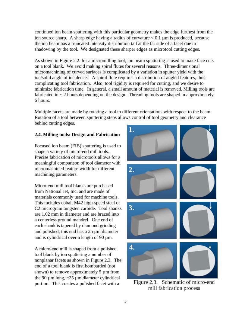
Figure 2.3. Schematic of micro-endmill fabrication process
1.
2.
3.
4.
continued ion beam sputtering with this particular geometry makes the edge furthest from theion source sharp. A sharp edge having a radius of curvature < 0.1 µm is produced, becausethe ion beam has a truncated intensity distribution tail at the far side of a facet due toshadowing by the tool. We designated these sharper edges as microtool cutting edges.
As shown in Figure 2.2. for a micromilling tool, ion beam sputtering is used to make face cutson a tool blank. We avoid making spiral flutes for several reasons. Three-dimensionalmicromachining of curved surfaces is complicated by a variation in sputter yield with theion/solid angle of incidence.5 A spiral flute requires a distribution of angled features, thuscomplicating tool fabrication. Also, tool rigidity is required for cutting, and we desire tominimize fabrication time. In general, a small amount of material is removed. Milling tools arefabricated in ~ 2 hours depending on the design. Threading tools are shaped in approximately6 hours.
Multiple facets are made by rotating a tool to different orientations with respect to the beam.Rotation of a tool between sputtering steps allows control of tool geometry and clearancebehind cutting edges.
2.4. Milling tools: Design and Fabrication
Focused ion beam (FIB) sputtering is used toshape a variety of micro-end mill tools.Precise fabrication of microtools allows for ameaningful comparison of tool diameter withmicromachined feature width for differentmachining parameters.
Micro-end mill tool blanks are purchasedfrom National Jet, Inc. and are made ofmaterials commonly used for machine tools.This includes cobalt M42 high-speed steel orC2 micrograin tungsten carbide. Tool shanksare 1.02 mm in diameter and are brazed intoa centerless ground mandrel. One end ofeach shank is tapered by diamond grindingand polished; this end has a 25 µm diameterand is cylindrical over a length of 90 µm.
A micro-end mill is shaped from a polishedtool blank by ion sputtering a number ofnonplanar facets as shown in Figure 2.3. Theend of a tool blank is first bombarded (notshown) to remove approximately 5 µm fromthe 90 µm long, ~25 µm diameter cylindricalportion. This creates a polished facet with a
6
normal direction oriented 7o with respect to the tool axis. This tool-end facet is intended toprovide clearance for chip removal during mechanical milling. After modifying the tool end,the ion beam is deflected over areas approximately 3 µm by 50-75 µm to create chip-cuttingfacets. With the FIB stage and tool fixed, the gallium beam impinges normal to a planecontaining the tool axis, but tangential to the tool circumference. As described in the previoussection, this ion-solid geometry is chosen, because it produces one extremely sharp edge perfacet. An SEM image showing a sub-µm radius of curvature is presented in Figure 2.4.
Numerous facets can be formed by sequentially rotating tools and sputtering. The number andposition of facets on a micro-end mill uniquely determine the properties of a tool, such asclearance for removing a chip and tool rotation direction for milling. Figure 2.5. shows micro-end mills having 2, 4 and 6 cutting facets made by focused ion beam sputtering. The tool inFigure 2.5.a. has two cutting facets and two diametrically opposed sharp edges. Figure 2.5.c.shows a tool having six cutting facets and clearance behind each of the five cutting edges, sincealmost the entire circumference is sputtered. In this study six-facet end mill tools are madewith 4, 5 or 6 sharp edges by selecting a particular stage rotation sequence between sputtersteps. The placement of facets by FIB sputtering determines tool rotation direction for milling
operations. Micro-end mills have been made so that sharp facet edges cut while rotating the
Figure 2.5. Micromilling tools shaped byfocused ion beam sputtering.
7
tool clockwise or counter-clockwise. Note, only tools made for a clockwise rotation (lookingdown on a workpiece) are tested.
Micromilling tools are fabricated in 2-3 hours depending on design and tool material. Ingeneral, a tool having a large number of facets is fabricated in a relatively short time, becauseless material is removed. For example, the time required to make the six-facet tool shown inFigure 2.5.c. is less than the time needed for the other tools shown. The fabrication timedepends on tool material, since sputter rate is a function of the target mass. The sputter ratefor tungsten carbide is quantified by bombarding polished wafers of identical C2-grade materialwith a fixed gallium dose equal to 1.0 x 10¹⁹ ions/cm2 (i= 2.8 nA) at 20keV. Areas 20 µm x20µm are sputtered to a small depth in order to avoid re-deposition, using a 72 µsec pixeldwell time, a 0.19 µm pixel spacing and a 0.86 sec refresh time. A single near-normal angle ofincidence is used for this control experiment. Afterwards, a portion of the feature is cross-sectioned with the gallium beam, and the depth is measured away from the feature edges.Average depth is measured by tilting the sample to a known angle in the scanning electronmicroscope and taking several measurements along the feature bottom boundary. Using thesputtered volume, an average rate of removal is calculated to be 0.76 µm3/sec.
When using FIB sputtering to fabricate microtools, it is important to note that each facet formsan angle of ~7 o with respect to the incident ion beam direction. (See Figure 2.3.) This occursbecause of minimal sputter yield at incidence angles greater than 83o with respect to the surfacenormal.6 Ions impinging on a surface at near-glancing angles most often reflect withoutdisplacing atoms from lattice sites. However, tools can be aligned with respect to the beamdirection in order to compensate for this sputter-induced angle.
2.5. Micromilling tools: Tests
Two high precision milling machines are used to test focused ion beam-fabricated tools and todevelop machining procedures. This includes a Boston Digital mill and a modified National Jet7M milling instrument.7 The Boston Digital apparatus has 1.0 µm resolution in the plane ofthe workpiece (x and y) and 0.5 µm depth resolution. Tools are held in a collet to minimizeerror. The National Jet 7M instrument has a 1500 kg granite machine base for vibrational andthermal stability, and all axes have air bearings. In addition, the x and y motions of the worktable employ laser interferometry with a commanded resolution of 1.25 nm, and the z motionhas linear encoder positional control with a resolution of 20 nm. All travel ranges are 150 mm.The micromilling head consists of a specially designed v-block bearing arrangement havingfour spherically convex diamonds. Tools rotate about an axis dictated by the contact positionsof the four diamond surfaces on the mandrel resulting in a cumulative radial error less than 1µm. The small error is attributed to variations in tool mandrel surface roughness. Allmicromachining tests involve a lubricant unless specified. Workpieces are flushed continuouslyduring micromilling with a water-based, sulfur free liquid (Blasser 4000). All millingoperations, including registry, are monitored with an optical microscope and CCD camera.
Scanning electron microscopy (SEM) and optical interferometry are used to analyzemicrotools and machined workpieces. A calibrated JEOL 6300V scanning electron microscope
8
is used to measure tool diameter, tool edge radius of curvature, trench widths and taper angles.This instrument is calibrated to a NIST/NBS standard (reference # 484 c) and shows less than2 % error for different working distances (i.e., bottom of pole piece to sample surface). Anoverall accuracy of 95 % or better is estimated for dimensions measured by SEM. Trenchwidths are measured from SEM images that view normal to the plane of a workpiece.Additional images that show perspective views are not used for measurement. PMMA samplesare coated with ~ 20 nm of Au/Pt to prevent charging in the SEM. A calibrated WYKO(RST+) white light optical interferometric roughness step tester determines the roughness inthe bottom of machined trenches. Several regions within the bottom of each micromachinedtrench are probed to obtain an accurate measurement of lateral and longitudinal surfaceroughness. A typical measured region is 100 µm long. PMMA samples coated with 20 nm ofAu/Pt have a reflective surface for inspection. The step height standard for the roughness steptester is a 23.33 µm metal film (VLSI Standards, Inc.). The phase shift interference resolutionof the RST+ is 0.3 nm.
Machining at feed rates of 2-3 mm/minute
In the present work micro-end mill tools are tested by milling materials having differentdegrees of machinability. Initial tests of micro-end mills involve machining at low feed rates, 2or 3 mm/minute, with an axial depth per pass > 0.5 µm. These depths/pass are chosen,because a microtool ‘appears’ sharp when compared to the cutting action, i.e., the tool edge Rc
is less than the thickness removed. Microtools are rotated clockwise in this study so that sharpfacet edges cut a workpiece.
50 µm
500 µm
b.
a.
10 µµm
0.5 mm
d.
c.
Figure 2.6..
Micromilled metal workpieces includingbrass (a. and b.) and 6061 Al alloy (c. and d.)
9
FIB-fabricated microtools successfully machine trenches in PMMA, aluminum, brass and 4340steel 8 at low feed rates. For all tests except for one, 15-25 µm deep trenches are cut severalmillimeters in length as commanded. Examples of micromachined metal workpieces are shownin Figure 2.6. This includes experiments on brass and 6061-T4 aluminum alloy. Assummarized in Table 1.2, the surface roughness (Ra) of most trenches machined at low feedrates is small, ~200 nm or less. In addition, all trenches milled in PMMA, Al alloy and 4340steel have nearly vertical sidewalls. Near-vertical sidewalls are present on both sides ofmicromachined trenches as demonstrated in 6061 Al (Figure 2.6.d.). Electron microscopyshows a slight taper of ~1-2o from vertical. SEM shows that micromachined trench widths aresimilar to the intended sizes (i.e., tool diameters). Experiments with the Boston Digitalapparatus produce trench widths that are ~2 µm larger than the tool diameters. Closematching is found for the different tool designs and workpiece materials. The small deviationfrom the intended width is attributed to the radial error of the tool and spindle. Thecombination of tool form error and spindle motion radial error is measured to be 2 µm or lessprior to each machining test. Error is probed approximately 2 mm from the end of the mandrelclosest to the tool shank using a test indicator. Additional milling tests with the modifiedNational Jet apparatus at large axial depths of cut and rotation speeds to 20,000 rpm producesimilar matching. Trenches milled in PMMA are limited at 2 µm larger than the tool diameter.With the National Jet instrument, a tool is held in a v-block bearing assembly that is speciallydesigned to minimize radial error beyond the variations in surface roughness of the toolmandrel. Therefore, we expect that the difference between the micro-end mill diameter andthe trench width results from the eccentricity of tool cutting edges and tool vibration. Ingeneral, tests with both milling instruments produce trench widths that are uniform overseveral millimeters. An example of this is shown in Figure 2.6.a. and b. The feature in brassrequires 25 passes for completion and demonstrates the positioning repeatability of ultra-precision milling instruments. Note that the curved portions of the micromachined trench, asseen in the SEM micrograph, are part of the intended design and are not image artifacts.
The experiments listed in Tables 2.1. show a single test that results in a significantly largertrench width and surface roughness. This involved tool ‘B2’, a two facet high speed steelmicro-end mill. Machining 6061 aluminum at a feed rate of 2 mm/ minute without a lubricantproduces a trench width approximately 6.4 µm larger than the tool diameter. Also, theroughness of the trench bottom is measured using optical interferometry to be ~458 nm. It isexpected that the lack of a lubricant is responsible for the poor characteristics of thismicromachined feature. Note, this ultra-precision machining test resulted in microtoolfracture, with breakage occuring during the twenty-second pass. It is estimated that tool B2 isrotated 3.4 x 10⁶ times while in contact with the workpiece prior to fracture. At the time oftool fracture, approximately 6.0 x 106 µm3 of material had been removed.
There are several indications from the experiments at low feed rates that microtools cut chipsrather than remove material by burnishing. In separate experiments on PMMA and 6061 Al,we turn off the lubricant and blow dry the workpiece for brief amounts of time to observecutting through an optical microscope. Repeatedly there is evidence of small chips beingejected from the vicinity of a moving tool. After rinsing workpieces, trenches are inspected
10
with SEM to determine the morphology of the bottom surface. In all cases, tool-cutting marksare revealed. Marks are found in micromachined brass, PMMA, Al alloy and steel.
Tool Code: H = Hex-tool (6 facets); B = Bi-tool (2 facets); Q = Quad-tool (4 facets)HSS = High Speed Steel; WC = tungsten carbide = No lubricant used during machining.
Table 2.1. Machining parameters and results from micromilling different materials at a feed rate of 2 or 3 mm/minute. Boston Digital apparatus is used.
Machining at feed rates of 3-50 mm/minute
Additional ultra-precision machining experiments are used to evaluate microtool performancefor increased chip load rates.9 Milling tests involve constant table feed rates of 3, 10, 25 and50 mm/minute, and again a tool is rotated clockwise (looking down on the workpiece) so thatsharp facet edges cut. A rotation speed of 18,000 rpm is used for each test, and the axial depthper pass is equal to 1.0 µm. For each feed rate, a single two-facet microtool mills 25 µm deep,7 mm long trenches in 6061-T4 Al. The tool is made of C2 tungsten carbide and has adiameter of 21.7 µm.
As described in Table 2.2., micromilled trench widths are approximately the same size as the tooldiameter. Average trench widths range from 22.0 to 23.1 µm. The standard deviation taken fromthese measurements is also included in the table. In addition, surface roughness measuredin the bottom of milled trenches is approximately 200 nm or less, and there is no degradationwith increased table feed rate. The morphology in the bottom is characterized by tool cuttingmarks. The sidewalls of this and other micromachined trenches are nearly vertical. Insummary, micromilling tests at higher feed rates suggest that FIB-fabricated microtools millmetal alloys without significant tool dulling. Repeated testing indicates that FIB-fabricatedtools are robust despite their small size and ‘apparent’ delicate nature. The two-facetmicrotool, labeled ‘B3’ in Table 2.2., milled 6061 Al for over 6 hours without tool fracture.For a feed rate of 50 mm/ min, aluminum alloy is machined at 18,740 µm3/sec.
Tool # Code: 1st letter designates overall shape; B = Bi-tool (2 facets)Tool Material Code: WC = tungsten carbide
Table 2.2. Machining parameters and results from micromilling Al 6061-T4 atdifferent feed rates including 3, 10, 25 and 50 mm /minute.
2.6 Microthreading/grooving tools: Design and Fabrication
Microthreading/grooving tools are fabricated from toolblanks made of cobalt M42 high-speed steel (HSS), C2micrograin tungsten carbide or single crystal diamond. Toolshanks made of WC or HSS have a diameter of 1.02 mm andare brazed into a centerless ground mandrel. Tool mandrelsare either 2.3 mm or 3.175 mm in diameter. One end of eachtool is tapered by diamond grinding and polished; this endhas a diameter of approximately 25 µm and is cylindrical overa length of 25 µm.
Microgrooving/threading tools have designs similar toconventional lathe cutting tools, however, cutting edgewidths are in the ~10-30 micron range. Each microtool isfabricated from a polished blank to have sharp cutting edges,clearance behind cutting edges and rake features. This isachieved by sputtering a number of strategically placed facetson cylindrical or conical sections at the end of a tool blank asshown in Figure 2.7. In general, the tool rotation/sputtersequence and the location of facets are critical for definingtool characteristics (rake, etc.). The first step of fabricatingall micro-grooving and micro-threading tools involvesshortening polished blanks. A smooth facet is sputtered atthe tool end. After sputtering, the end facet normal is nearlyaligned with the tool axis. Next, two facets are created onopposite sides of a tool. This sputter step determines thecutting width, tool cross-section and, hence, the intendedcross-sectional shape of a micromachined groove. Forexample, ion milling two nearly-parallel facets creates a tool
1.0 mm
a.
b.
10 µµm
10 µµm
c.
Figure 2.7 Micro-grooving/threadingtool made of tungsten carbide. Tool hasrectangular cross-section with an 18µmwide tool end cutting edge.
12
Figure 2.8. High speed steel toolsspeedttoolmicrotool having a trapezoidal cross-section.
10 µµm
30 µµm
100 µµm
a.
b.
c.
with a rectangular cutting shape. Alternatively a threading tool that cuts trapezoidal cross-section grooves is fabricated by ion milling two nonparallel facets. Sputtering side facets withthe geometry described is also critical for establishing taper. Taper provides clearance behindside facet cutting edges thus minimizing contact with workpieces and reducing frictional dragon a tool. During sputtering, each side facet forms a natural taper angle of ~ 5-10o withrespect to the ion beam direction as for the milling tools.
After creating side facets, the focused ion beam is used to define rake features that clear chipsduring ultra-precision machining. First, each tool is rotated -90oin the FIB system. Thisorients one side facet away from the ion source and places the second side facet such that itnearly faces the source. A triangular projected area is then ion milled on one side of a tool todefine a desired back rake angle. The FIB system can accurately define this angle with aresolution of 0.25o. In this study, micro-grooving tools are made with a back rake anglebetween 0 and 10o, referenced to the tool axis. Tools are made to have a 0o back rake angle inorder to increase rigidity. FIB sputtering is also used during this step to set the rake facetlength, typically 10-20 µm. Note, a natural taper angle of ~ 5-10o with respect to the ion beamdirection accompanies rake feature definition,independent of the back rake angle chosen. Thistaper can be used to establish side rake, displayedin an end-on view of a tool, Figure 2.7.c. The siderake angle can be changed or eliminated, i.e.,forced to 0o, by proper rotation of the stage / toolprior to ion milling this facet.
A sharp cutting edge having clearance is created atthe microtool end as a final step of fabrication.Tools are first rotated to their original orientationwith respect to the ion beam, and the length isreduced approximately 3 µm by sputtering. Thiscreates an end facet that intersects the rake facetat a well-defined, sharp edge. Measurements fromSEM show this edge has a radius of curvature (Rc)of 0.4 µm or less. Radii are measured by viewingparallel to the cutting edge. In addition tocreating a sharp edge for cutting, this ion millingstep establishes clearance. A taper angle of ~ 5-10o behind the tool end cutting edge preventsunnecessary contact with workpieces.
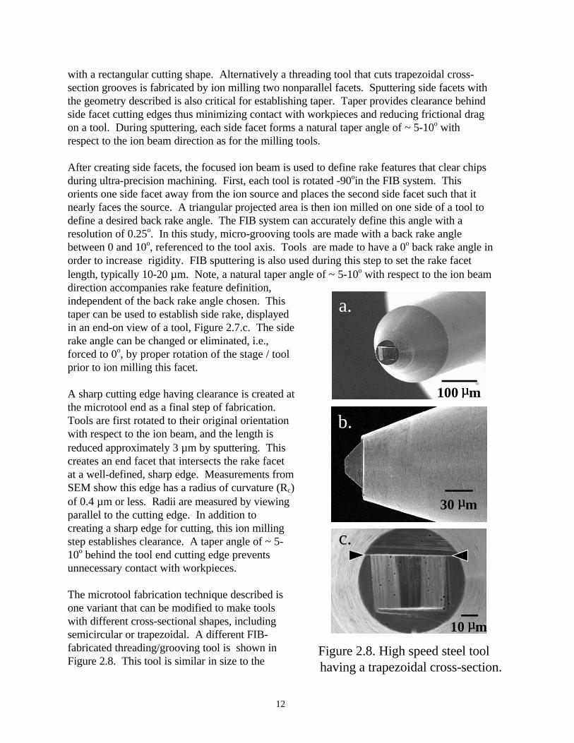
The microtool fabrication technique described isone variant that can be modified to make toolswith different cross-sectional shapes, includingsemicircular or trapezoidal. A different FIB-fabricated threading/grooving tool is shown inFigure 2.8. This tool is similar in size to the
13
microtool shown in Figure 2.7.; however, this has a trapezoidal cross-section and 0o rakeangles. The images in Figure 2.8. show three cutting edges, similar to a stub-threading tool.The side facet cutting edges are oriented 90o apart, and the leading edge of the tool is 15 µmwide. The taper behind cutting edges is displayed in a secondary electron micrograph of thetool end, Figure 2.8.c.
The small but detectable roughness of cutting facets is due to ion beam sputtering. Mostlikely, the compositional inhomogeneity of tungsten carbide and high speed steel affects thesmoothness. Track marks can develop along facets during sputtering because of shadowing bysecond phase particles (or other compositional variations) within a tool. For example, cobalt ispresent in C2-grade tungsten carbide and has a different sputter yield compared with thematrix. Fabricated microtools are polycrystalline with grains oriented in different directions.Track marks and compositional variations within C2 tungsten carbide are seen in Figure 2.7.b.and c. In these SEM micrographs, regions that have a low electron yield appear dark. Energy-dispersive x-ray spectroscopy reveals that the low yield features in Figure 2.7. are Co–rich andC-rich regions. We expect that sharper tool cutting edges can be achieved by focused ionbeam sputtering of other tool materials. Single crystal materials (e.g., diamond) should exhibitminimal variation in sputter yield from point to point due to compositional uniformity.
2.7 Microthreading/grooving tools: Tests
This section describes a number of experiments that test the performance of focused ion beamfabricated microtools. Tests involve machining helical features in polymer, ceramic and metalworkpieces.
Ultra-precision turning involves a Precitech Optimum 2000 high precision lathe (LouisianaTech University, courtesy of Professor Michael Vasile). The Precitech lathe operates withboth the x and z axis drive mechanisms mounted on a granite platform lapped co-planar to 1.3µm and isolated from the machine frame to prevent unwanted vibrations. Identical fully-constrained, dovetail-type air bearing slides provide smooth motion for the two axes with lessthan 0.25 µm deviation per 102 mm of motion. The total length of travel is 191 mm and themaximum slide speed is 1000 mm/min. The two slides are oriented perpendicular to within 2arc-seconds. Linear laser holographic scales and read-head assemblies provide stablepositional feedback for both axes with 8.6 nm resolution. The spindle is supported by fullypre-loaded, high stiffness air bearings and is driven by an integrally mounted brushless DCmotor and encoder with range from 0 to 5000 rpm. In order to accurately ‘touch-off’,operations are monitored with an optical microscope and CCD camera. Water continuouslyflushes workpieces during ultra-precision machining. After machining, workpieces are rinsedwith isopropyl alcohol. However, in this study burrs are not removed by mechanical orelectrochemical polishing.
Microthreading tools and certain micromachined workpieces are analyzed by scanning electronmicroscopy (SEM). An overall accuracy of 95 % or better is estimated for dimensionsmeasured by an Amray 1830 scanning electron microscope. This microscope is calibrated to aNIST SRM 2090 standard in the 100 µm range and shows a –2.4 % to –2.6 % error when
14
using a fixed working distance (i.e., bottom of pole piece to sample surface). In addition, acalibrated JEOL 6300V scanning electron microscope is used to measure widths of groovesmachined in cylindrical workpieces. This instrument is calibrated to a NIST/NBS standard(reference # 484 c) and shows less than 2 % error for different working distances. The widthsof grooves machined in cylindrical workpieces are determined by viewing feature cross-section.
FIB-fabricated, micro-grooving/threading tools are tested by machining helical grooves indifferent cylindrical workpieces.10 A polished, cylindrical workpiece is mounted into a pin viceconcentric with the lathe axis of rotation, and a tool holder post is arranged perpendicular.The workpiece is first polished to run true on the lathe, using a diamond bit; this establishes aworkpiece surface finish of approximately 1µm (rms) or better. Afterwards, a FIB-fabricatedmicrotool is loaded and aligned with its axis perpendicular to the workpiece axis. Using ascribe mark on the mandrel for alignment, the tool is then rotated to an orientation such thatthe tool-end cutting edge is nearly parallel to the workpiece axis. An alignment accuracy oftool cutting edges to better than 0.5o ensures minimal contact of side facets with the groovewall. The microtool is then stepped toward the rotating workpiece and registered. Once theworkpiece is contacted, the tool is driven into the workpiece to a targeted groove depth andlinear motion is initiated.
Using this technique, micro-grooving tools cut helical grooves into cylindrical samples made of6061-T6 aluminum alloy. Figure 2.9.a. shows a portion of a 13.2 µm wide, 4 µm deep groovehaving a total length of 200 mm. The pitch between successive passes is 100 µm and is set bythe relative rotation rate and the axial feed rate.A change in pitch can be achieved by simplyincreasing/decreasing these rates. Electronmicroscopy demonstrates a close match of toolsize and micromachined feature width.Measurements show that the groove width isapproximately the same as the cutting edgewidth, 13.0 µm, over the length of the feature.Also, high magnification images demonstrateclose matching of tool shape and feature cross-section. SEM analysis of the micromachinedgroove bottom shows a 6o taper with respect tothe cylinder axis. This is identical to the angleof the tool-end cutting edge.
A precise matching of tool shape and groovecross-section also results from machiningpolymeric cylindrical workpieces. Figure 2.9.b.shows portions of a groove cut in 1.38 mmdiameter PMMA. The pitch is 50 µm and thetotal groove length is 420 mm. The total timeto cut PMMA is approximately 30 seconds.
250µµmb.
0.5 mm
a.
Figure 2.9. Cylindrical workpieces machinedwith lathe microtool. Helical grooves are
fabricated into (a.) Al 6061 and (b.) PMMA.
15
SEM measurements show that the micromachined groove is consistently 13.1 µm wide overthe entire cylinder length, and nearly the same as the tool width, 13.0 µm. In addition, SEMindicates a uniform 6o taper throughout the groove bottom, closely matching the shape of thetool end. Optical interferometry indicates that the roughness in the bottom of machinedgrooves remains small, similar to that for aluminum. By analyzing a number of line scansacross the micromachined groove, the average rms roughness is measured to be 0.25 µm.Analysis of microtools immediately after machining cylindrical workpieces reveals that chipsare cut and raked away from workpiece surfaces. An indication of this is shown in Figure2.10.a. which displays a long PMMA chip wrapped around the shank of a microtool. The chipwidth is approximately equal to the cutting edge width. Additional SEM at highermagnification indicates chip raking. Figure 2.10.b. shows aluminum chips deflected by a rakefacet with minimal accumulation behind the tool-end cutting edge.
The techniques used for making micro-end mills and microthreading tools are capable offabricating even smaller tools. Beam sizes for the FIB system are 0.4 µm, and positioningresolution is better than 1 µm. Tools made to smaller dimensions must have suitablemicrostructures that provide strength and toughness necessary for cutting.
2.8 Ion milling of curvilinear shapes
A new microfabrication capability has been added to the focused ion beam system. Thisincludes software that allows for sputtering of prespecified ‘3-dimensional’ shapes.(Xie andVasile) In the past, focused ion beam sputtering has been restricted to milling of rectilinear orprismatic cross-sections. Potentially the ability to fabricate curved features will allow for moregeometrically-complex micro-cutting tools and features required in complex,microelectromechanical devices.
The code allows the user to sputter curvilinear shapes including sinusoids, hemispheres andparabolas of different sizes and symmetry. This is accomplished by numerically solving for the
20µµm
b.
100µµm
a.
Figure 2.10. Scanning electronmicrographs of micro-groovingtools after machining PMMA (a.) and 6061-T6 aluminum (b.).
16
beam pixel dwell times required to sputter a shape of a given depth. The calculation of iondose required at each pixel within the targeted area accounts for the sputter yield dependenceon incidence angle, the sputter yield dependence on material properties and the ion beamintensity distribution. The creation of curved surfaces in initially planar substrates can consistof a large range of incidence angle depending on the depth and net shape. In general, eachtarget material has different sputter yield dependencies.
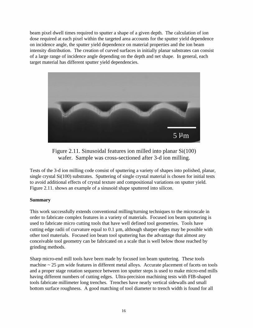
Tests of the 3-d ion milling code consist of sputtering a variety of shapes into polished, planar,single crystal Si(100) substrates. Sputtering of single crystal material is chosen for initial teststo avoid additional effects of crystal texture and compositional variations on sputter yield.Figure 2.11. shows an example of a sinusoid shape sputtered into silicon.
Summary
This work successfully extends conventional milling/turning techniques to the microscale inorder to fabricate complex features in a variety of materials. Focused ion beam sputtering isused to fabricate micro cutting tools that have well defined tool geometries. Tools havecutting edge radii of curvature equal to 0.1 µm, although sharper edges may be possible withother tool materials. Focused ion beam tool sputtering has the advantage that almost anyconceivable tool geometry can be fabricated on a scale that is well below those reached bygrinding methods.
Sharp micro-end mill tools have been made by focused ion beam sputtering. These toolsmachine ~ 25 µm wide features in different metal alloys. Accurate placement of facets on toolsand a proper stage rotation sequence between ion sputter steps is used to make micro-end millshaving different numbers of cutting edges. Ultra-precision machining tests with FIB-shapedtools fabricate millimeter long trenches. Trenches have nearly vertical sidewalls and smallbottom surface roughness. A good matching of tool diameter to trench width is found for all
5 µm
Figure 2.11. Sinusoidal features ion milled into planar Si(100)wafer. Sample was cross-sectioned after 3-d ion milling.
17
materials tested including PMMA, 6061 Al, 4340 steel and brass. This includes machining attable feed rates up to 50 mm/minute.
In addition, this study has fabricated and tested several types of microthreading/ micro-grooving tools. These successfully machine helices in cylindrical workpieces. Feature cross-section closely matches tool shape when machining PMMA, Macor and aluminum alloy.These results suggest that other microtools, for example those having nonorthogonal cuttingedges, can accurately fabricate beveled grooves with a given desired cross-section.
References:
1. See for example, Minitool, Inc., Los Gatos, CA, USA.2. Vasile MJ, Biddick C, and Schwalm SA, Microfabrication by ion milling: The lathe technique,
J. Vac. Sci. Technol. B, 1994; 12, 2388.3. Harriott LR, A second generation focused ion beam micromachining system, Proc. SPIE,
1987; 773, 190.4. Vasile MJ, Friedrich CR, Kikkeri B, and McElhannon R, Micrometer-scale machining: tool
fabrication and initial results, Precision Engineering, 1996; 19 (2/3), 180-186. Friedrich CRand Vasile MJ, Development of the micromilling process for high aspect ratio microstructures,J. Microelectromech. Sys., 1996; 5, 33-38.
5. Vasile MJ, Nassar R, Niu Z, Zhang W, and Liu S, Focused ion beam milling: depth control forthree-dimensional microfabrication, J. Vac. Sci. Technol. B, 1997; 15, 2350-2354.
6. Vasile MJ, Nassar R, Xie J, and Guo H, Microfabrication techniques using focused ion beamsand emergent applications, Micron, 1999; 30, 235-244.
7. The second apparatus was a joint project among Louisiana Tech University (IfM), the NationalJet Company and Dover Instruments.
8. Hardness values for the different metal alloy workpiece materials include 6061-T4 aluminum,Rockwell B =26; brass, Rockwell B = 35; 4340 steel, Rockwell B = 97
9. D.P. Adams, M.J. Vasile, G. Benavides, and A.N. Campbell, Micromilling of metal alloys withfocused ion beam-fabricated tools, Precision Engineering, 2001, 25, 107-113.
10. D.P. Adams, M.J. Vasile, and A.S.M. Krishnan, Microgrooving and microthreading tools forfabricating curvilinear features, Precision Engineering, 2000, 24, 347-356.
18
Intentionally Left Blank.
19
3.0 Laser Machining
The key issue of using lasers for micro-machining is to minimize the heat affected zone (HAZ)surrounding the ablated micro-feature. Because a huge amount of energy is deposited at themachined area on the work-piece, a large melting zone can be created due to the thermaldiffusion. Such an effect significantly reduces the precision and accuracy required for themicro-machining operation. To minimize this detrimental effect, two approaches wereidentified and used in this study. The first approach is to minimize the penetration depth byusing a short wave length laser. This can be achieved by excimer lasers (XeC, KrF, and ArFwith wave lengths that vary from 308 nm to 192 nm) where most energy can only be absorbednear to the surface1. The second approach is to use an ultra-short pulse laser, such as a femto-second laser, where the time scale is too short for the thermal energy to be transferred from thefast electron cooling to the crystalline lattice.2 Since both mechanisms only permit a shortthermal diffusion length, the ablation process is more efficient and material can be preciselyremoved layer-by-layer. Figure 3.1 illustrates this removal operation on alumina by an excimerlaser where the machining depth is linearly proportional to the number of laser pulses. Asimilar phenomenon is also observed by femto-second laser ablation where each pulse creates agroove-like appearance on the drilling wall of a 5 mil kovar sheet (see Figure 3.2). This layer-by-layer ablation provides a precision control of drilling depth and creates a unique capabilityto machine three dimensional micro-features.
Sandia has an excimer laser (Lumonics Hyperex-400, 248nm) set up for meso-scale machining.The excimer laser machines material by pulsing it with nanosecond pulses (10-25 ns) ofultraviolet light. The workpiece is mounted to precision translational stages which iscontrolled by a CAD/CAM system. A controller coordinates the motion of the workpiecerelative to the stationary UV laser beam and coordinates the firing of the pulses. Figure 3.3 isa schematic setup for a mask projection technique that is used to define machining geometries.The mask is inserted into the excimer laser beam where the fluence is too low to ablate themask. The pattern geometry on the mask is de-magnified through the lens and projected onto
Distance (µm)
0 200 400 600 800 1000 1200
Sca
le (
µm)
-50
0
50
100
150
200
250
300100 pulses
200 pulses
300 pulses
400 pulses
500 pulses
Number of pulses
0 100 200 300 400 500 600
Dep
th (
µm)
0
10
20
30
40
50
Figure 3.1: (a) The cross-section profiles of excimer laser (KrF)machining on alumina, (b) The number of laser pulses verses themachining depth.
20
the work piece. An internal aperture is introduced to reduce the beam divergence which inturn effectively reduces the spot size and enhances the edge definition of a projected image.This approach can be used to machine multiple holes simultaneously. Figure 3.4 is an image ofan array of 48 micron holes simultaneously machined into alumina.
Figure 3.2: A Micro-hole (~3.2 µm) machined in kovar using a Ti-sapphirefemto-second laser. Each pulse removes about 0.2 µm of kovar layer.
X-Y stagesFocus control (Z)
Laser firing
Diaphrag
Beam
Energy
CCD
Processing
CAD/CAM
Excimer Laser
Internal
External
Mask
Mirro
Pris
Figure 3.3 Schematic experimental setup for excimer laser micromachining.
21
Figure 3.4: An array of 48 micron holesmachined into 275 micron thick aluminausing excimer laser mask projection (24mJ/pulse at 30 Hz in air).
Sandia’s excimer laser has been used to machinepolymers, ceramics, glass, and metals. Thegeneral ablation behavior of ceramic, metal, andglass is given in Figure 3.5. For alumina(Figure 3.5 (a)) and stainless steel (Figure 3.5(b)), the ablation rate quickly increases afterpassing the ablation threshold, then ablation rateremains constant as fluence increases. Theenergy density for machining operation isselected at the lowest fluence level where theablation rate holds constant. This gives areproducible result without stressing the lasersystem. When a modern excimer laser system isused where the repetition rate can reach up to 2000 pulses per second, it is possible to achievean ablation rate of 40,000 cubic microns per second. In contrast to the above materials, theablation rate of a PZT (lead zirconate titanate) ceramic and a lead glass increases drasticallyafter passing the ablation threshold then decreases as the fluence increases (Figure 3.5 (c)). Itis believed that the electron density for the plasmas created over the glass or PZT ceramicduring laser processing is greater than 1.8 X 1028 m-3 (at wavelenght =248 nm).3 Under suchcircumstance, the reflection and scattering increases with the laser fluence, thus the incidentradiation is significantly attenuated through the plasma.3 Consequently, the ablation ratedecreases. The ablation thresholds and the material removal rates for various materials aresummarized in Table 3.1. Figure 3.6 (a) and (b) shows the microphotographs of a 25 micronby 25 micron channel machined by the excimer laser into alumina and PZT ceramics. Thevertical walls in the channel are a result of good coupling.of the UV wavelength (248 nm) tothe ceramic materials.
Fluence (J/cm2)
0 5 10 15 20 25
Alb
latio
n ra
te (
µm3 /p
ulse
)
0
10
20
30
40
(a) alumina
Fluence (J/cm2)
1 2 3 4 5
Abl
atio
n ra
te (
µm3/p
ulse
)
0.0
0.5
1.0
1.5
2.0
(b) stainless steel
Fluence (J/cm2)
0 2 4 6 8 10 12 14
Abl
atio
n ra
te (
µm3 /p
ulse
)
20
30
40
50
60PZT ceramicslead glass
(c) PZT and lead glass
Figure 3.5: The ablation ratesfor (a) alumina ,(b) stainlesssteel, (c) PZT and lead glass inair (KrF, 248 nm).
22
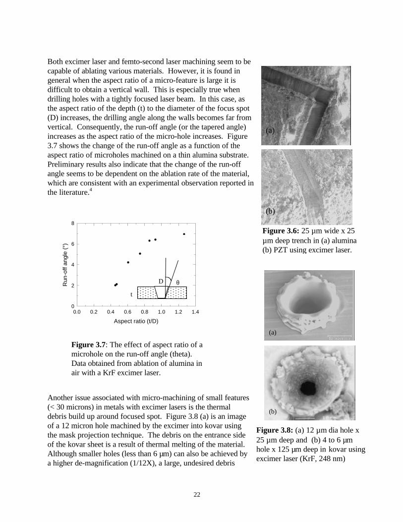
Both excimer laser and femto-second laser machining seem to becapable of ablating various materials. However, it is found ingeneral when the aspect ratio of a micro-feature is large it isdifficult to obtain a vertical wall. This is especially true whendrilling holes with a tightly focused laser beam. In this case, asthe aspect ratio of the depth (t) to the diameter of the focus spot(D) increases, the drilling angle along the walls becomes far fromvertical. Consequently, the run-off angle (or the tapered angle)increases as the aspect ratio of the micro-hole increases. Figure3.7 shows the change of the run-off angle as a function of theaspect ratio of microholes machined on a thin alumina substrate.Preliminary results also indicate that the change of the run-offangle seems to be dependent on the ablation rate of the material,which are consistent with an experimental observation reported inthe literature.4
Another issue associated with micro-machining of small features(< 30 microns) in metals with excimer lasers is the thermaldebris build up around focused spot. Figure 3.8 (a) is an imageof a 12 micron hole machined by the excimer into kovar usingthe mask projection technique. The debris on the entrance sideof the kovar sheet is a result of thermal melting of the material.Although smaller holes (less than 6 µm) can also be achieved bya higher de-magnification (1/12X), a large, undesired debris
Figure 3.8: (a) 12 µm dia hole x25 µm deep and (b) 4 to 6 µmhole x 125 µm deep in kovar usingexcimer laser (KrF, 248 nm)
(a)
(b)
Figure 3.7: The effect of aspect ratio of amicrohole on the run-off angle (theta).Data obtained from ablation of alumina inair with a KrF excimer laser.
Aspect ratio (t/D)
0.0 0.2 0.4 0.6 0.8 1.0 1.2 1.4
Run
-off
angl
e (°
)
0
2
4
6
8
θ
t
D
Figure 3.6: 25 µm wide x 25µm deep trench in (a) alumina(b) PZT using excimer laser.
(a)
(b)
23
Figure 3.9: Collaboration with PulsedPower (SNL): Micro-holes machined in kovarusing a Ti:sapphire system (120 femtoseconds)in air (a.) and in vacuum (b.). These arecompared with a hole. All images are takenfrom the entry side of the foil.
10 µµm
a. b.
10 µµm
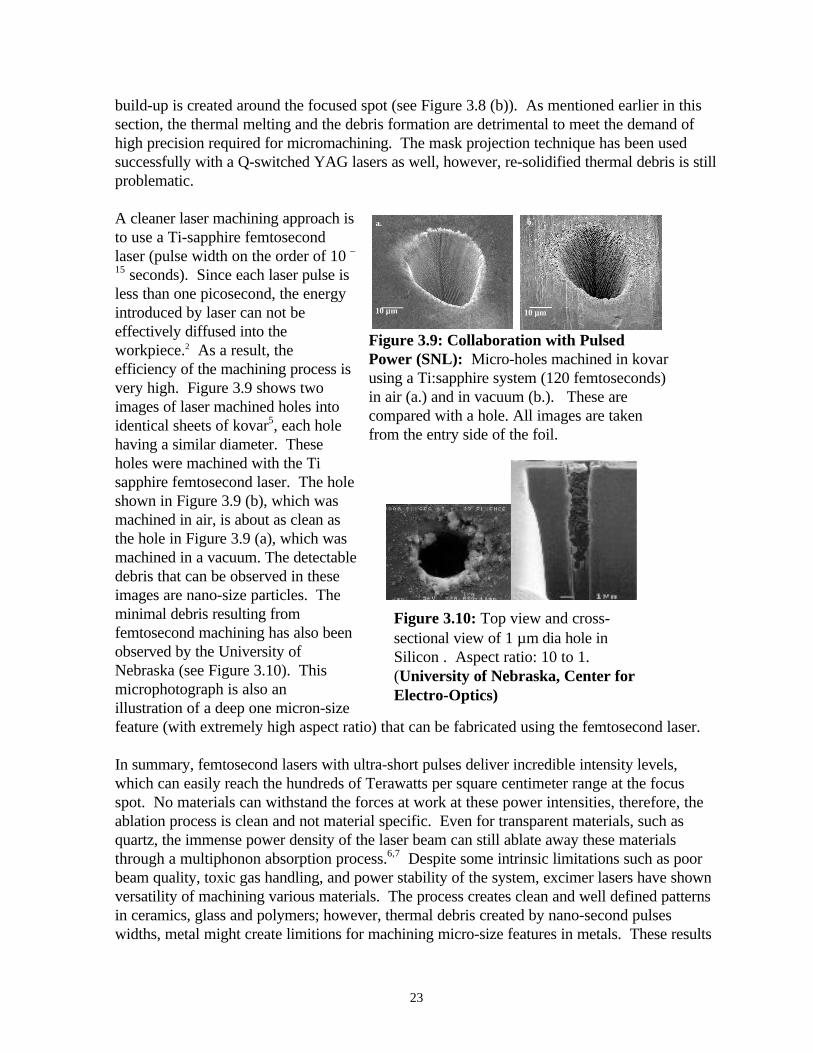
Figure 3.10: Top view and cross-sectional view of 1 µm dia hole inSilicon . Aspect ratio: 10 to 1.(University of Nebraska, Center forElectro-Optics)
build-up is created around the focused spot (see Figure 3.8 (b)). As mentioned earlier in thissection, the thermal melting and the debris formation are detrimental to meet the demand ofhigh precision required for micromachining. The mask projection technique has been usedsuccessfully with a Q-switched YAG lasers as well, however, re-solidified thermal debris is stillproblematic.
A cleaner laser machining approach isto use a Ti-sapphire femtosecondlaser (pulse width on the order of 10 –
15 seconds). Since each laser pulse isless than one picosecond, the energyintroduced by laser can not beeffectively diffused into theworkpiece.2 As a result, theefficiency of the machining process isvery high. Figure 3.9 shows twoimages of laser machined holes intoidentical sheets of kovar5, each holehaving a similar diameter. Theseholes were machined with the Tisapphire femtosecond laser. The holeshown in Figure 3.9 (b), which wasmachined in air, is about as clean asthe hole in Figure 3.9 (a), which wasmachined in a vacuum. The detectabledebris that can be observed in theseimages are nano-size particles. Theminimal debris resulting fromfemtosecond machining has also beenobserved by the University ofNebraska (see Figure 3.10). Thismicrophotograph is also anillustration of a deep one micron-sizefeature (with extremely high aspect ratio) that can be fabricated using the femtosecond laser.
In summary, femtosecond lasers with ultra-short pulses deliver incredible intensity levels,which can easily reach the hundreds of Terawatts per square centimeter range at the focusspot. No materials can withstand the forces at work at these power intensities, therefore, theablation process is clean and not material specific. Even for transparent materials, such asquartz, the immense power density of the laser beam can still ablate away these materialsthrough a multiphonon absorption process.6,7 Despite some intrinsic limitations such as poorbeam quality, toxic gas handling, and power stability of the system, excimer lasers have shownversatility of machining various materials. The process creates clean and well defined patternsin ceramics, glass and polymers; however, thermal debris created by nano-second pulseswidths, metal might create limitions for machining micro-size features in metals. These results
24
indicate that short pulse lasers (in the range of sub-picosecond range (<10-12 second)) arerequired for patterning of high thermally conducting materials in order to obtain high precisionand minimize thermal damage.
Kovar 0.7 1.2 @ fluence > 2.8 J/cm2 † at the maximum ablation rate.
Reference:1. W. W. Duley, UV Lasers: Effects and Application in Materials Science, Cambridge
University Press, Cambridge, UK (1996).2. B. N Chichkov, C. Momma, S. Nolte, F. von Alvenseben, and A. Tunnermann, "
Femtosecond, Picosecond and Nanosecond Laser Ablation of Solids," Appl. Phys. A, 63,109 (1996).
3. R. Poprawe, E. Beyer, and F. Herziger, Inst. Phys. Conf. Ser., 72, 87 (1984).4. M. Eyett and D. Bauerle, "Influence of Beam Spot Size on Ablation Rates in Pulsed-Laser
Processing", Appl. Phys. Lett, 51, (24), 2054 (1987).5. D. E. Bliss, D. P. Adams, S. M. Cameron, and T. S. Luk, "Laser Machining with
Ultrashort Pulses: Effects of Pulse-Width, Frequency and Energy," Material Science ofMicroelectromechanical Systems (MEMS) Devices, Mat. Res. Soc. Symp. Proc., Vol 546(1999).
6. J. Ihlemann, B. Wolff, and P. Simon, "Nanosecond and Femtosecond Excimer Laserablation of Fused Silica", Appl. Phys. A, 54, 363 (1992).
7. H. Varel, D. Ashkenasi, A. Rosenfeld, M. Wahmer, and E. E. B. Campbell,"Micromachining of Quartz with Ultrashort Laser Pulses," Appl. Phys. A., 65, 367 (1997).
25
4.0 Micro-EDM (electro-discharge machining)
Electro-discharge machining removes material through a spark erosion process. The micro-EDM machines can machine features as small as 25 microns because the micro-generatorneeded to create the spark has the necessary fine control to minimize the energy per pulse forthe smaller features. These low energy pulses sent in rapid succession not only producesmaller features but also minimize the surface roughness to about 0.1 microns Ra. For eitherthe sinker or the wire micro-EDM machine, the two major considerations for determiningfeature size are the electrode size and the over-burn gap. Sandia has used electrodes as smallas 25 microns in diameter and over-burn as little as 3 microns. Currently, Sandia has an AgieCompact 1, micro-sinker EDM machine (see figure 4.1) and an Agie Excellence 2F micro-capable wire EDM machine (see figure 4.2). The advantage to the sinker EDM process is thatan electrode having a complex three-dimensional geometry can be sunk into a work piececreating the conformal geometry in the work piece. A disadvantage to the sinker EDM is thatthe electrode also erodes during the EDM process (although at a much slower rate). Verticalside-walls are more difficult with the sinker EDM process due to electrode wear. Theadvantage to the wire EDM process is that unused wire can be circulated to the work pieceduring the EDM process thereby presenting to the work piece an electrode having a knowngeometry. The disadvantage to the wire EDM process is that the feature cuts are usually of asimpler geometry (two and a half dimensional). Although, the Agie Excellence 2F wiremachine can make a somewhat more complex cut because of its ability to tilt the wire (4th axiscapable).
Creating an electrode having a complex geometry for the sinker EDM machine is not trivial.Graphite is a very desirable electrode material because it machines easily and it erodes slowly(i.e., the work piece erodes quickly but the electrode maintains its shape longer). Also,hundreds of complex finely featured graphite electrodes can be fabricated from one master dieby way of ultrasonic grinding. Features as small as 50 microns can be ultrasonically groundinto high density finely grained graphite. Copper is also very common electrode material.Another approach to fabricating a complicated sinker micro EDM electrode for a meso-scalepart is to use the LIGA process. LIGA is a lithographic process that additively builds meso-scale parts by electroplating material into molds. Copper, which is a good performingelectrode material, can be plated into LIGA molds. The copper LIGA fabricated electrode canthen be mounted onto the sinker micro-EDM machine to fabricate a part in yet a differentmaterial such as stainless steel or kovar. This hybrid process is a method of extending thematerial base for LIGA.
Figure 4.3 is an image of a small intricate copper electrode fabricated by the LIGA process.This electrode was then used to EDM through a .006 inch thick kovar sheet. If the electrodecan be described as the bricks then the machined work piece would be the “mortar” that fitsbetween the bricks. Figures 4.4 and 4.5 respectively show the entrance side and the exit sideof the kovar part. The most challenging feature on the kovar part is the portion of the“mortar” that is .002 inch thick by .006 inch deep (measured into the page). A parametricstudy was performed to determine the optimal over burn gap that yields an acceptable part
Figure 4.4: Entrance side of kovar part. Figure 4.5: Exit side of kovar part.
Figure 4.3: Micro-EDM electrode incopper made with the LIGA process.
27
machined within a reasonable time. A relationship exists between the over-burn gap and themachining time. The smaller the over-burn gap the finer the features but the greater the timerequired to machine the part. The kovar part was machined with copper electrodes having anover-burn gap of .0005 inch, .001 inch, .0015 inch, and .002 inch. The over-burn gapparameter can easily be varied by under sizing the LIGA fabricated electrode to thecorresponding gap. The .0015 inch over-burn gap was a compromise which resulted in a goodpart that was machined in about 15 minutes.
Both graphite and copper are good electrode materials but for different reasons. Desirableelectrodes maintain their shape longer and therefore do not need to be replaced as often for afresh electrode when machining multiple parts. Material properties for a desirable electrodeinclude high heat conductivity, high specific heat, and high melting point. Graphite obviouslyexcels in regards to melting point while copper readily conducts heat. The ultrasonicallyground graphite electrode produced a part similar to that shown in figures 4.4 and 4.5,however, the graphite electrode maintained its shape better than copper.
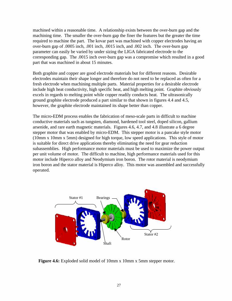
The micro-EDM process enables the fabrication of meso-scale parts in difficult to machineconductive materials such as tungsten, diamond, hardened tool steel, doped silicon, galliumarsenide, and rare earth magnetic materials. Figures 4.6, 4.7, and 4.8 illustrate a 6 degreestepper motor that was enabled by micro-EDM. This stepper motor is a pancake style motor(10mm x 10mm x 5mm) designed for high torque, low speed applications. This style of motoris suitable for direct drive applications thereby eliminating the need for gear reductionsubassemblies. High performance motor materials must be used to maximize the power outputper unit volume of motor. The difficult to machine, high performance materials used for thismotor include Hiperco alloy and Neodymium iron boron. The rotor material is neodymiumiron boron and the stator material is Hiperco alloy. This motor was assembled and successfullyoperated.
Figure 4.6: Exploded solid model of 10mm x 10mm x 5mm stepper motor.
Stator #1 Bearings
RotorStator #2
Shaft
Stator #1 Bearings
RotorStator #2
Shaft
28
The important parameters for EDM in general include, pulse energy, pulse rate, polarity,electrode material, dielectric fluid, over-burn gap, and flushing. The pulse energy has its ownset of parameters such as voltage, current, and pulse duration. The pulse energy controls thesize of crater eroded from the work piece. The pulse rate is a major factor that controls howquickly material is removed. The pulse rate must allow for sufficient time between pulses sothat the dielectric fluid has time to recover (i.e. de-ionize) and for particles to be flushed away.The polarity which defines whether the electrode is the cathode or anode can greatly affect therelative erosion rate of the electrode versus the work piece (i.e., electrode wear). The over-burn gap is a dependent parameter that can be controlled by varying the voltage/current profileduring a pulse. A smaller over-burn gap requires a smaller breakdown voltage. An importantconsideration that is sometimes difficult to implement for the micro EDM process, is flushing.Particles that are being generated during the EDM process need to be flushed away from theover-burn gap region. These particles can quickly accumulate and create an electrical shortbetween the electrode and the work piece. Particles are typically flushed away by circulatingthe dielectric fluid through the over-burn gap region. For over-burn gaps as small as 3microns, it is sometimes difficult to flush the particles away. The flushing problem is moreprominent in regards to the sinker micro-EDM process rather than the wire micro-EDM.
Reference:1. J.P. Kruth, F. Staelens, “Non-traditional Machining Methods, Electro-Discharge
Machining”, Katholieke Universiteit Leuven, 1993-1994.2. H.C. Moser, B. Boehmert, “Trends in EDM”, Modern Machine Shop Feb. 20003. K. Takahata, N. Shibaike, H. Guckel, “High-aspect-ratio WC-Co microstruture produced
by the combination of LIGA and micro-EDM”, Microsystems Technologies 6 (2000) 175-178.
As in the macro world, no one meso-scale machining process can do it all. Some meso-scaleprocesses are more encompassing than others, but each process has its niche. As in the macroworld, designers usually require a variety of materials to optimize performance of mechanicalcomponents. For example hermeticity and corrosion resistance may be importantcharacteristics for housing (or packaging) materials but wear and friction characteristics maybe important for gears internal to the housing. Gears and housings made from non-magneticmaterials are desirable when used in the vicinity of electromagnetic actuators. Table 5.1 is anattempt by the authors to summarize meso-machining processes. The data in the table is meantto be a representation of the technology but does not represent any particular machinemanufacturer. The first column in the table lists the technology and also whether thetechnology can fabricate 3D features or 2D (actually 2.5D) features only. The second columnindicates minimum feature size and the tolerance associated with that feature. For example theminimum feature size for micro-milling is 25 microns channel plus or minus 2 microns. Thesource for the tolerance assigned to micro-milling is a result of the radial run out of the toolwhen mounted in the collet. The third column lists the feature positional tolerance, which ismostly based upon the quality of positional stages used on the machine, however, work pieceset-up accuracy also plays a role. In the example of micro-milling, the 25 micron channel canbe positioned on the work piece to plus or minus 3 microns. The fourth column lists thematerial removal rate, which is an indicator of how quickly parts can be machined. The FIBhas a very poor material removal rate, which was a driver for using the FIB to fabricate micro-tools. Although it can take a long time to make a micro-tool, the micro-tool has a highmaterial removal rate and can be used for a significant duration (up to six hours). A featuretolerance and feature positional tolerance of about 3 microns does not compare favorably withLIGA. Nevertheless, a 3 micron profile tolerance on ratchet teeth (for example) on a 6 mmdiameter part is an equivalent ratio to a .001 inch profile tolerance on a 2 inch diameter part.The point is, 3 microns is probably plenty good enough.
Meso-machining processes can create true three dimensional piece parts. As an example, asingle part can be fabricated having a gear, hub, and shaft. The meso-machining process caneliminate the need to assemble a shaft and hub to the gear which is a difficult assembly. Pressfits for meso-scale parts requires only microns of interference. Meso-machining can eliminatethe need to press fit a shaft. Meso-machining processes offer the best relative tolerancecapabilities for precision parts (i.e., the tolerance of the dimension, normalized by thedimension). The relative tolerance capability of silicon based MEMS processes is aboutequivalent to the relative tolerances used to build a house.
Electroformable: copper, nickel, permalloy (see note)
Note: LIGA can also be used to fabricate parts in polymers, pressed pow ders, ceramics, and rare-earth magnets w ith a little degradation in machining performance specifications.
Table 5.1: Comparison of meso-machining processes.
References:1. Marc Madou, “Precision Machining Applications Domain”, Fundamentals of
Microfabrication, CRC Press, 1997
2. "Nanotribology: Critical Assessments and research needs", edited by S. M. Hsu, KluwerAcademic Press, Boston, MA, USA, to be published in Oct. 2000.
31
6.0 ISSUES
Designers are comfortable with traditional materials (e.g. stainless steel) because thesematerials have a long history and have been very well characterized through the years. Meso-scale machining processes allow the designer to use traditional materials. On the other hand,tribological issues for meso-scale parts may or may not emulate what is already known.Subtractive meso-scale machining technologies expand the material base and increase thecombinations of materials that can come into contact. Galling may be an issue with somematerial combinations. Each particular meso-scale machining process uniquely affects thesurface roughness and morphology. Micro-milling and micro-turning may generate burrs andparticles that can cause mechanical interference. Micro-EDM may leave a recast layer that canhave either favorable or unfavorable wear and friction characteristics. Friction effects of meso-scale parts sliding with other parts may have limited points of contact and are not accuratelymodeled by surface contact models. Some meso-scale machining technologies, such as micro-EDM, are fairly mature, while others, such as femtosecond laser machining, require additionaldevelopment. Material stability may be of greater concern for high precision, low aspect ratioparts. For example, a very thin gear may warp like a potato chip upon being machined if thematerial stress relieves. A number of stable non-magnetic materials are being considered formeso-scale parts, such as, Nitronic 60 stainless steel, Titanium, and Beryllium Copper.Machine tool forces are a non-issue for meso-machining processes such as femtosecond lasermachining and micro-EDM and therefore do not contribute to the deformation of meso-scaleparts. Many issues have yet to be identified.
32
Intentionally Left Blank.
33
Distribution:
5 MS 0958 Gil Benavides, 141845 MS 0959 Pin Yang, 141925 MS 0959 David Adams, 141711 MS 0319 Charles Vanecek, 26131 MS 0960 Norm DeMeza, 141001 MS 0961 Carol Adkins, 14101
1 MS 0188 LDRD Office, Attn: Donna Chavez1 MS 9018 Central Technical Files, 8945-12 MS 0899 Technical Library, 96161 MS 0612 Review & Approval Desk, 9612