Sumit Chaudhary,2,3,4 David Lynch,2 Kai-Ming Ho,2,3 and Kristen Constant1,2,* 1Department of Materials Science and Engineering, Iowa State University, Ames, Iowa 50011, USA
2USDOE – Ames Laboratory, Iowa State University, Ames, Iowa 50011, USA 3Department of Physics and Astronomy, Iowa State University, Ames, Iowa 50011, USA
4Department of Electrical and Computer Engineering, Iowa State University, Ames, Iowa 50011, USA *[email protected]
Abstract: A novel architecture has been employed to fabricate transparent electrodes with high conductivity and high optical transmittance at high incident angles. Soft lithography is used to fabricate polymer grating patterns onto which thin metallic films are deposited. Etching removes excess metal leaving tall walls of metal. Polymer encapsulation of the structure both protects the metal and minimizes diffraction. Transmission is dependent upon the height of the walls and encapsulation and varies from 60% to 80% for structures with heights of 1400 nm to 300 nm. In encapsulated structures, very little distortion is visible (either parallel to or perpendicular to standing walls) even at viewing angles 60° from the normal. Diffraction is at characterized through measurement of intensity for zeroth through third order diffraction spots. Encapsulation is shown to significantly reduce diffraction. Measurements are supported by optical simulations.
References and links 1. B. G. Lewis and D. C. Paine, “Applications and processing of transparent conducting oxides,” MRS Bull. 25(08),
22–27 (2000). 2. T. Minami, “New n-type transparent conducting oxides,” MRS Bull. 25(08), 38–44 (2000). 3. M. Katayama, “TFT-LCD technology,” Thin Solid Films 341(1-2), 140–147 (1999). 4. D. E. Carlson and C. R. Wronski, “Amorphous silicon solar-cell,” Appl. Phys. Lett. 28(11), 671–673 (1976). 5. C. G. Granqvist and A. Hultaker, “Transparent and conducting ITO films: new developments and applications,”
Thin Solid Films 411(1), 1–5 (2002). 6. “Critical materials strategy summary,” Department of Energy, USA (2011). http://energy.gov/pi/office-policy-
and-international-affairs/downloads/2011-critical-materials-strategy 7. Y. Leterrier, L. Medico, F. Demarco, J. A. E. Manson, U. Betz, M. F. Escola, M. K. Olsson, and F. Atamny,
“Mechanical integrity of transparent conductive oxide films for flexible polymer-based displays,” Thin Solid Films 460(1-2), 156–166 (2004).
8. C. Guillen and J. Herrero, “Influence of the film thickness on the structure, optical and electrical properties of ITO coatings deposited by sputtering at room temperature on glass and plastic substrates,” Semicond Sci Ech 23(7), 075002 (2008).
9. M. W. Rowell, M. A. Topinka, M. D. McGehee, H. J. Prall, G. Dennler, N. S. Sariciftci, L. B. Hu, and G. Gruner, “Organic solar cells with carbon nanotube network electrodes,” Appl. Phys. Lett. 88(23), 233506 (2006).
10. J. B. Wu, H. A. Becerril, Z. N. Bao, Z. F. Liu, Y. S. Chen, and P. Peumans, “Organic solar cells with solution-processed graphene transparent electrodes,” Appl. Phys. Lett. 92(26), 263302 (2008).
11. J. Y. Lee, S. T. Connor, Y. Cui, and P. Peumans, “Solution-processed metal nanowire mesh transparent electrodes,” Nano Lett. 8(2), 689–692 (2008).
12. M. G. Kang and L. J. Guo, “Nanoimprinted semitransparent metal electrodes and their application in organic light-emitting diodes,” Adv. Mater. (Deerfield Beach Fla.) 19(10), 1391–1396 (2007).
13. M. G. Kang, M. S. Kim, J. S. Kim, and L. J. Guo, “Organic solar cells using nanoimprinted transparent metal electrodes,” Adv. Mater. (Deerfield Beach Fla.) 20(23), 4408–4413 (2008).
#175042 - $15.00 USD Received 30 Aug 2012; revised 2 Dec 2012; accepted 4 Dec 2012; published 24 Jan 2013(C) 2013 OSA 28 January 2013 / Vol. 21, No. 2 / OPTICS EXPRESS 2393
14. M. G. Kang, H. J. Park, S. H. Ahn, and L. J. Guo, “Transparent Cu nanowire mesh electrode on flexible substrates fabricated by transfer printing and its application in organic solar cells,” Sol. Energy Mater. Sol. Cells 94(6), 1179–1184 (2010).
15. S. H. Ahn and L. J. Guo, “High-speed roll-to-roll nanoimprint lithography on flexible plastic substrates,” Adv. Mater. (Deerfield Beach Fla.) 20(11), 2044–2049 (2008).
16. A. Chutinan and S. John, “Light trapping and absorption optimization in certain thin-film photonic crystal architectures,” Phys. Rev. A 78(2), 023825 (2008).
17. Y. C. Shin, D. H. Kim, E. H. Kim, J.-M. Park, K.-M. Ho, K. P. Constant, J. H. Choe, Q. H. Park, H.-Y. Ryu, J. H. Baek, T. Jung, and T. G. Kim, “High efficiency GaN light-emitting diodes with two dimensional photonic crystal structures of deep-hole square lattices,” IEEE J. Quantum Electron. 46(1), 116–120 (2010).
18. J. H. Lee, C. H. Kim, K. M. Ho, and K. Constant, “Two-polymer microtransfer molding for highly layered microstructures,” Adv. Mater. (Deerfield Beach Fla.) 17(20), 2481–2485 (2005).
19. P. Kuang, J. M. Park, W. Leung, R. C. Mahadevapuram, K. S. Nalwa, T. G. Kim, S. Chaudhary, K. M. Ho, and K. Constant, “A new achitecture for transparent electrodes: relieving the trade-off between electrical conductivity and optical transmittance,” Adv. Mater. (Deerfield Beach Fla.) 23(21), 2469–2473 (2011).
20. Movie clip: http://home.engineering.iastate.edu/~sumitc/documents/electrodes. 21. Z. Y. Li and L. L. Lin, “Photonic band structures solved by a plane-wave-based transfer-matrix method,” Phys.
Rev. E Stat. Nonlin. Soft Matter Phys. 67(4), 046607 (2003). 22. M. Li, X. H. Hu, Z. Ye, K. M. Ho, J. R. Cao, and M. Miyawaki, “Higher-order incidence transfer matrix method
used in three-dimensional photonic crystal coupled-resonator array simulation,” Opt. Lett. 31(23), 3498–3500 (2006).
23. Z. Ye, X. H. Hu, M. Li, K. M. Ho, and P. D. Yang, “Propagation of guided modes in curved nanoribbon waveguides,” Appl. Phys. Lett. 89(24), 241108 (2006).
24. C. R. Pichard, C. R. Tellier, and A. J. Tosser, “A three-Dimensional model for grain-boundary resistivity in metal-films,” Thin Solid Films 62(2), 189–194 (1979).
25. P. M. T. M. van Attekum, P. H. Woerlee, G. C. Verkade, and A. A. M. Hoeben, “Influence of grain-boundaries and surface Debye temperature on the electrical-resistance of thin gold-films,” Phys. Rev. B 29(2), 645–650 (1984).
1. Introduction
Transparent conducting electrodes with a combination of high optical transmission and high electrical conductivity are essential and desirable in solar energy harvesting and optoelectronic applications. Transparent conducting oxides (TCOs) are wide bandgap materials that offer high transparency for visible light and relatively good electronic conduction [1]. Indium tin oxide (ITO) and zinc oxide (ZnO) are typical oxide materials used for such purposes [2]. ITO is widely used in flat panel displays and solar cells, but it is also found in heat mirrors and smart-window applications due to its excellent infrared reflection properties [3–5]. However, there are several drawbacks to using ITO. It is costly due to limited indium resources [6]. The brittle nature of the oxide has also limited its potential use in various novel devices such as flexible solar cells and flexible displays [7]. There is a trade-off between the optical and electrical properties of ITO dependent on the film thickness [8]. These disadvantages have motivated the search for alternative conducting electrodes with similar or better performance. In recent research efforts, carbon nanotube networks, graphene films, silver nanowire meshes and nanopatterned metal grids have been evaluated as potential replacements for ITO based electrodes [9–12]. In particular, nanopatterned metal grids made by nano-imprinting techniques are showing promise because of the straightforward and effective process and its amenability to roll-to-roll printing for large area fabrication [12–15]. Different microscale or nanoscale patterning techniques are being examined to investigate other possible fabrication processes for patterned structures such as transparent electrodes. Due to their light manipulation capabilities, photonic crystal structures show promise in solar radiation collection and absorption for photovoltaic devices and outcoupling efficiency enhancement in solid-state lighting [16,17]. Various patterning and fabrication techniques to make such photonic structures and their optical properties have been investigated. One simple and cost-effective method utilizes soft lithography [18].
Recently, we reported a new architecture consisting of transparent nanoscale high aspect-ratio metallic photonic structures fabricated via a combination of processes, including soft lithography, oblique angle metal deposition and argon plasma ion etching [19]. The optical
#175042 - $15.00 USD Received 30 Aug 2012; revised 2 Dec 2012; accepted 4 Dec 2012; published 24 Jan 2013(C) 2013 OSA 28 January 2013 / Vol. 21, No. 2 / OPTICS EXPRESS 2394
and electrical properties of these structures were characterized and evaluated to determine their applicability as transparent electrodes. In this report, the optical properties of such structures are investigated in detail to examine their transmission at different incident angles. We also evaluate the encapsulation process to reduced diffraction from these structures for solid-state lighting and smart window applications.
2. Experimental
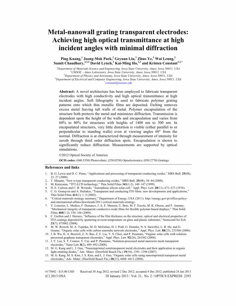
One-dimensional (1D) photoresist (PR) grating patterns of 2.5 μm periodicity, 1.2 μm width, and either ~1400 nm or 300 nm height were used to make a PDMS mold following a previously reported soft lithography process [18]. Then the PDMS (polydimethylsiloxane) mold was used to replicate the grating pattern in polyurethane (PU). The PU prepolymer was first dispensed onto a transparent substrate, and then the PDMS mold was brought into contact and mechanically pressed onto the prepolymer. The PU was solidified by UV curing. The PDMS mold was then peeled off of the PU, transferring the 1D grating pattern. During the molding process, excess PU forms an underlayer below the patterned structure (Fig. 1). This process is not suitable for structure inversion because that underlayer, when exposed, would seal off the channels in the structure. Nevertheless, in cases that don’t require inversion, this approach is simple and cost-effective for some applications.
Fig. 1. Schematics for metal deposition, argon plasma etching, and encapsulation process.
After the PU grating structure is fabricated, multiple metal depositions are carried out to form gold (Au) coatings on the PU surface (Fig. 1). The deposition rate for was maintained at 0.1 nm/s to ensure homogeneous metal coating. Both sputtering and angle evaporation can be applied for the metallization step. Argon plasma etching is performed to remove the metal from the PU top surface and/or in the channels of the grating structure. The etching process is highly anisotropic, so only the metal on top and in the channels is etched but the metal sidewalls remains intact. For applications such as solid-state lighting and smart windows, diffraction from the grating structure must be minimized. We hypothesized that this can be done through an encapsulation process. To encapsulate, additional PU liquid prepolymer was placed on top of the etched structure and UV cured, with a second glass substrate enclosing the entire structure. The additional PU fills the air channels between the metal sidewalls to reduce diffraction from the grating pattern. The optical transmission of the samples was measured with a 3 inch Labsphere integrating sphere with an Ocean Optics S2000 spectrometer with and without a polarizer.
#175042 - $15.00 USD Received 30 Aug 2012; revised 2 Dec 2012; accepted 4 Dec 2012; published 24 Jan 2013(C) 2013 OSA 28 January 2013 / Vol. 21, No. 2 / OPTICS EXPRESS 2395
3. Results and discussion
Fabricated structures were characterized to determine the effect on properties of a number of parameters including the effect of the height of the structure, encapsulation, and angle of incidence on optical transmission. Diffraction intensity measurements were also performed to characterize the extent of diffraction for encapsulated and unencapsulated structures.
3.1 Effect of height on optical transmission
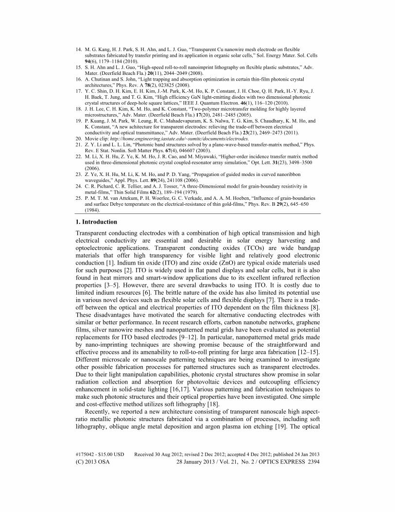
Figure 2(a) shows the transmission spectra of samples with 1400 nm height before plasma etching at around 40-45%. With argon plasma etching, the maximum transmission obtained was around 60%. The improved transmission is mainly due to the metal removal on top of PU bars and the reduction in reflection. However, this transmission is still relatively low. This is because while the metal on top of PU bars is being etched, the PU underlayer in the channels is also exposed to argon ions and it is also etched by them. This will create a much deeper trough in the channels and enhance the diffraction effect of the grating structure. Furthermore, for the PU grating where the metal top is removed, the PU material in between the two metal sidewalls is also etched if the process is not stopped. However, when the structure is encapsulated, PU prepolymer fills inside the channels and significantly reduces diffraction. In this case, the measured total transmission is improved to above 70% for wavelengths beyond 600 nm. For the 300 nm height structure, the transmission is 60% before etching. After plasma etching, the total transmission is increased to about 77%. With encapsulation, the transmission intensity was further increased to 80%. Comparing to previously published results, for the taller structure, the total transmission is 10% less than ion milled samples with much smaller areas [19]. The plasma etching is not as effective as the argon ion milling because the argon plasma etching was done at low power (100 watts) for longer times, which results in damage to the polymer during etching. It is likely that a higher power argon plasma etcher would result in better etching for large area samples.
Fig. 2. The measured transmission spectra for structures (a) with 1400nm height (b) and with 300nm height with gold sidewalls before and after plasma etching.
3.2 Effect of encapsulation on optical transmission
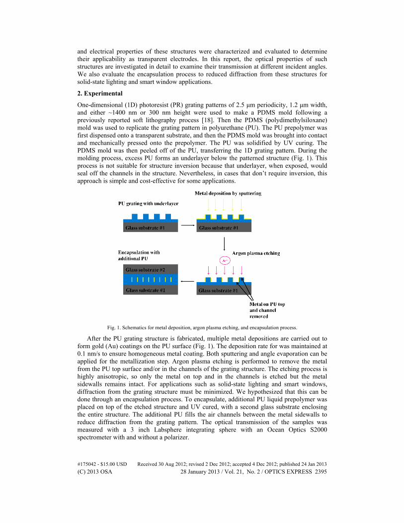
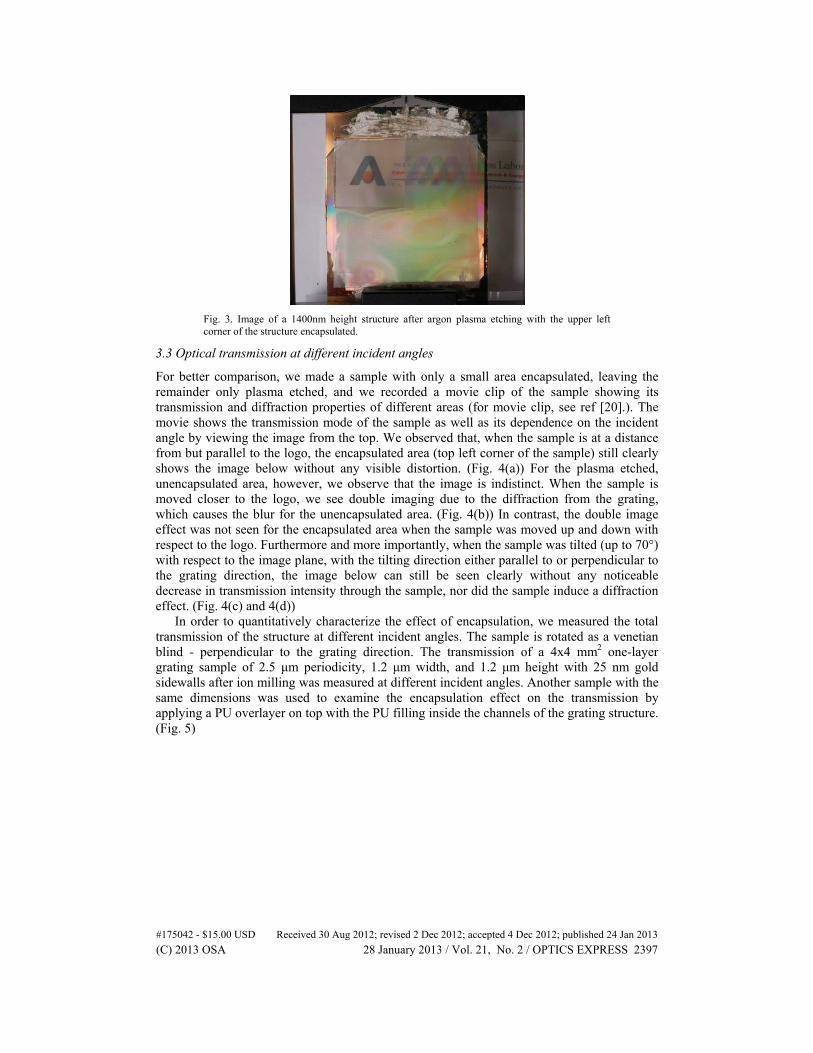
To show the optical property differences between the unencapsulated and encapsulated structure, a plasma etched sample was partially encapsulated in one corner. Two identical logos are placed below and about 3 cm away from the sample (Fig. 3). For the unencapsulated area on the right, a double image is apparent due to the diffraction of the grating structure. For the encapsulated area, the image has little distortion. The diffraction effect is vastly reduced. This approach demonstrates that the structure, when encapsulated, is suitable for transparent electrode applications in solid-state lighting and smart windows.
#175042 - $15.00 USD Received 30 Aug 2012; revised 2 Dec 2012; accepted 4 Dec 2012; published 24 Jan 2013(C) 2013 OSA 28 January 2013 / Vol. 21, No. 2 / OPTICS EXPRESS 2396
Fig. 3. Image of a 1400nm height structure after argon plasma etching with the upper left corner of the structure encapsulated.
3.3 Optical transmission at different incident angles
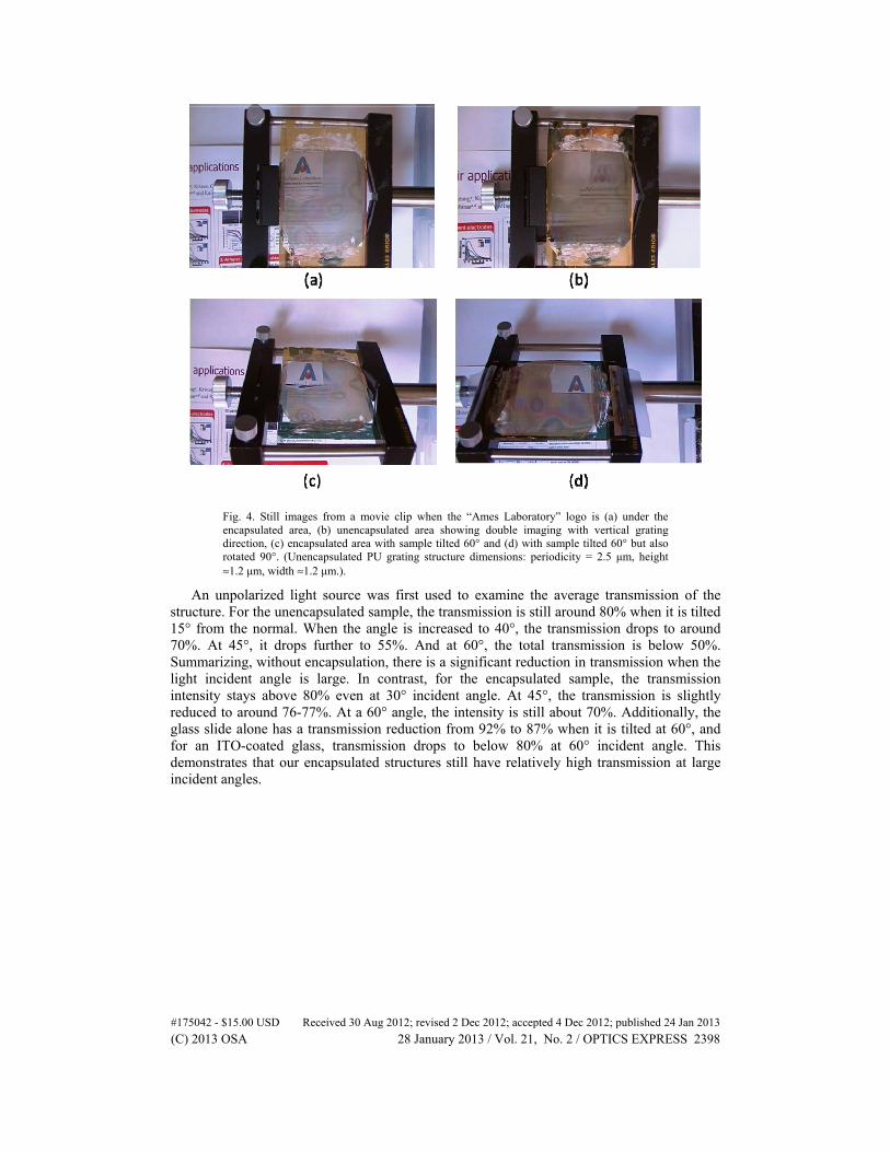
For better comparison, we made a sample with only a small area encapsulated, leaving the remainder only plasma etched, and we recorded a movie clip of the sample showing its transmission and diffraction properties of different areas (for movie clip, see ref [20].). The movie shows the transmission mode of the sample as well as its dependence on the incident angle by viewing the image from the top. We observed that, when the sample is at a distance from but parallel to the logo, the encapsulated area (top left corner of the sample) still clearly shows the image below without any visible distortion. (Fig. 4(a)) For the plasma etched, unencapsulated area, however, we observe that the image is indistinct. When the sample is moved closer to the logo, we see double imaging due to the diffraction from the grating, which causes the blur for the unencapsulated area. (Fig. 4(b)) In contrast, the double image effect was not seen for the encapsulated area when the sample was moved up and down with respect to the logo. Furthermore and more importantly, when the sample was tilted (up to 70°) with respect to the image plane, with the tilting direction either parallel to or perpendicular to the grating direction, the image below can still be seen clearly without any noticeable decrease in transmission intensity through the sample, nor did the sample induce a diffraction effect. (Fig. 4(c) and 4(d))
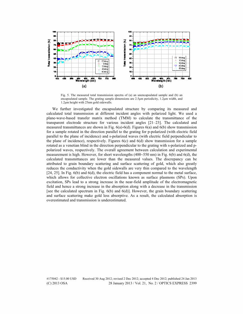
In order to quantitatively characterize the effect of encapsulation, we measured the total transmission of the structure at different incident angles. The sample is rotated as a venetian blind - perpendicular to the grating direction. The transmission of a 4x4 mm2 one-layer grating sample of 2.5 μm periodicity, 1.2 μm width, and 1.2 μm height with 25 nm gold sidewalls after ion milling was measured at different incident angles. Another sample with the same dimensions was used to examine the encapsulation effect on the transmission by applying a PU overlayer on top with the PU filling inside the channels of the grating structure. (Fig. 5)
#175042 - $15.00 USD Received 30 Aug 2012; revised 2 Dec 2012; accepted 4 Dec 2012; published 24 Jan 2013(C) 2013 OSA 28 January 2013 / Vol. 21, No. 2 / OPTICS EXPRESS 2397
Fig. 4. Still images from a movie clip when the “Ames Laboratory” logo is (a) under the encapsulated area, (b) unencapsulated area showing double imaging with vertical grating direction, (c) encapsulated area with sample tilted 60° and (d) with sample tilted 60° but also rotated 90°. (Unencapsulated PU grating structure dimensions: periodicity = 2.5 μm, height ≈1.2 μm, width ≈1.2 μm.).
An unpolarized light source was first used to examine the average transmission of the structure. For the unencapsulated sample, the transmission is still around 80% when it is tilted 15° from the normal. When the angle is increased to 40°, the transmission drops to around 70%. At 45°, it drops further to 55%. And at 60°, the total transmission is below 50%. Summarizing, without encapsulation, there is a significant reduction in transmission when the light incident angle is large. In contrast, for the encapsulated sample, the transmission intensity stays above 80% even at 30° incident angle. At 45°, the transmission is slightly reduced to around 76-77%. At a 60° angle, the intensity is still about 70%. Additionally, the glass slide alone has a transmission reduction from 92% to 87% when it is tilted at 60°, and for an ITO-coated glass, transmission drops to below 80% at 60° incident angle. This demonstrates that our encapsulated structures still have relatively high transmission at large incident angles.
#175042 - $15.00 USD Received 30 Aug 2012; revised 2 Dec 2012; accepted 4 Dec 2012; published 24 Jan 2013(C) 2013 OSA 28 January 2013 / Vol. 21, No. 2 / OPTICS EXPRESS 2398
Fig. 5. The measured total transmission spectra of (a) an unencapsulated sample and (b) an encapsulated sample. The grating sample dimensions are 2.5μm periodicity, 1.2μm width, and 1.2μm height with 25nm gold sidewalls.
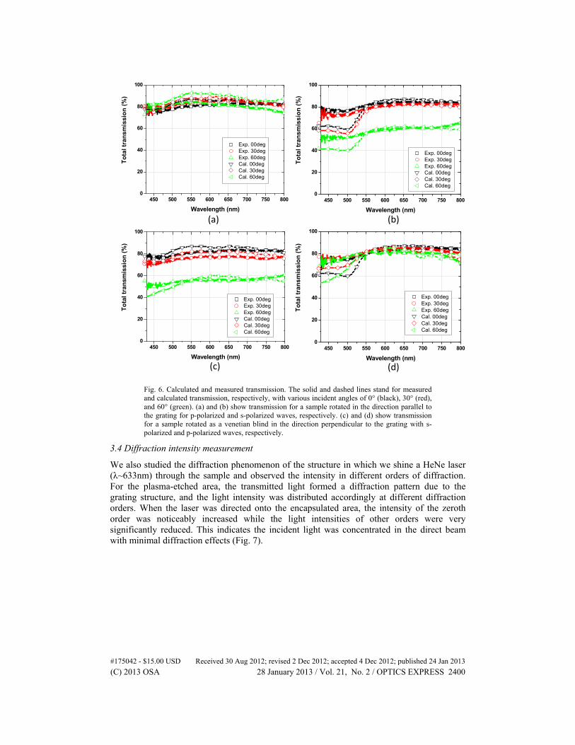
We further investigated the encapsulated structure by comparing its measured and calculated total transmission at different incident angles with polarized light. We used a plane-wave-based transfer matrix method (TMM) to calculate the transmittance of the transparent electrode structure for various incident angles [21–23]. The calculated and measured transmittances are shown in Fig. 6(a)-6(d). Figures 6(a) and 6(b) show transmission for a sample rotated in the direction parallel to the grating for p-polarized (with electric field parallel to the plane of incidence) and s-polarized waves (with electric field perpendicular to the plane of incidence), respectively. Figures 6(c) and 6(d) show transmission for a sample rotated as a venetian blind in the direction perpendicular to the grating with s-polarized and p-polarized waves, respectively. The overall agreement between calculation and experimental measurement is high. However, for short wavelengths (400~550 nm) in Fig. 6(b) and 6(d), the calculated transmittances are lower than the measured values. The discrepancy can be attributed to grain boundary scattering and surface scattering of gold, which also greatly reduces the conductivity when the gold sidewalls are very thin compared to the wavelength [24, 25]. In Fig. 6(b) and 6(d), the electric field has a component normal to the metal surface, which allows for collective electron oscillations known as surface plasmons (SPs). Upon excitation, SPs lead to a strong increase in the near-field amplitude of the electromagnetic field and hence a strong increase in the absorption along with a decrease in the transmission [see the calculated spectrum in Fig. 6(b) and 6(d)]. However, the grain boundary scattering and surface scattering make gold less absorptive. As a result, the calculated absorption is overestimated and transmission is underestimated.
#175042 - $15.00 USD Received 30 Aug 2012; revised 2 Dec 2012; accepted 4 Dec 2012; published 24 Jan 2013(C) 2013 OSA 28 January 2013 / Vol. 21, No. 2 / OPTICS EXPRESS 2399
Fig. 6. Calculated and measured transmission. The solid and dashed lines stand for measured and calculated transmission, respectively, with various incident angles of 0° (black), 30° (red), and 60° (green). (a) and (b) show transmission for a sample rotated in the direction parallel to the grating for p-polarized and s-polarized waves, respectively. (c) and (d) show transmission for a sample rotated as a venetian blind in the direction perpendicular to the grating with s-polarized and p-polarized waves, respectively.
3.4 Diffraction intensity measurement
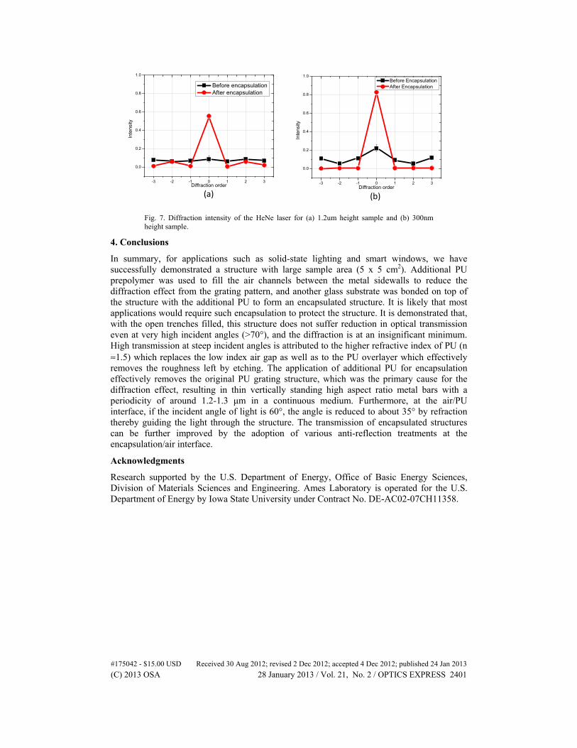
We also studied the diffraction phenomenon of the structure in which we shine a HeNe laser (λ~633nm) through the sample and observed the intensity in different orders of diffraction. For the plasma-etched area, the transmitted light formed a diffraction pattern due to the grating structure, and the light intensity was distributed accordingly at different diffraction orders. When the laser was directed onto the encapsulated area, the intensity of the zeroth order was noticeably increased while the light intensities of other orders were very significantly reduced. This indicates the incident light was concentrated in the direct beam with minimal diffraction effects (Fig. 7).
#175042 - $15.00 USD Received 30 Aug 2012; revised 2 Dec 2012; accepted 4 Dec 2012; published 24 Jan 2013(C) 2013 OSA 28 January 2013 / Vol. 21, No. 2 / OPTICS EXPRESS 2400
-3 -2 -1 0 1 2 3
0.0
0.2
0.4
0.6
0.8
1.0
Inte
nsity
Diffraction order
Before encapsulation After encapsulation
-3 -2 -1 0 1 2 3
0.0
0.2
0.4
0.6
0.8
1.0
Inte
nsity
Diffraction order
Before Encapsulation After Encapsulation
(a) (b)
Fig. 7. Diffraction intensity of the HeNe laser for (a) 1.2um height sample and (b) 300nm height sample.
4. Conclusions
In summary, for applications such as solid-state lighting and smart windows, we have successfully demonstrated a structure with large sample area (5 x 5 cm2). Additional PU prepolymer was used to fill the air channels between the metal sidewalls to reduce the diffraction effect from the grating pattern, and another glass substrate was bonded on top of the structure with the additional PU to form an encapsulated structure. It is likely that most applications would require such encapsulation to protect the structure. It is demonstrated that, with the open trenches filled, this structure does not suffer reduction in optical transmission even at very high incident angles (>70°), and the diffraction is at an insignificant minimum. High transmission at steep incident angles is attributed to the higher refractive index of PU (n ≈1.5) which replaces the low index air gap as well as to the PU overlayer which effectively removes the roughness left by etching. The application of additional PU for encapsulation effectively removes the original PU grating structure, which was the primary cause for the diffraction effect, resulting in thin vertically standing high aspect ratio metal bars with a periodicity of around 1.2-1.3 μm in a continuous medium. Furthermore, at the air/PU interface, if the incident angle of light is 60°, the angle is reduced to about 35° by refraction thereby guiding the light through the structure. The transmission of encapsulated structures can be further improved by the adoption of various anti-reflection treatments at the encapsulation/air interface.
Acknowledgments
Research supported by the U.S. Department of Energy, Office of Basic Energy Sciences, Division of Materials Sciences and Engineering. Ames Laboratory is operated for the U.S. Department of Energy by Iowa State University under Contract No. DE-AC02-07CH11358.
#175042 - $15.00 USD Received 30 Aug 2012; revised 2 Dec 2012; accepted 4 Dec 2012; published 24 Jan 2013(C) 2013 OSA 28 January 2013 / Vol. 21, No. 2 / OPTICS EXPRESS 2401