Page 1
www.pandianprabu.weebly.com Page 1
MF9211 ADVANCED MATERIALS TECHNOLOGY UNIT.V- NON METALLIC MATERIALS
POLYMERS & COMPOSITES
Materials
Extensive materials experience includes:
Thermoplastic polymers
o Hydrocarbon polymers
Polyethylene (PE)
HDPE
LDPE
Polypropylene (PP)
Atactic
Isotactic
Polybutadiene
Syndiotatctic
Isotactic
Polystyrene (PS)
Atactic
Isotactic
o Nonhydrocarbon carbon-chain polymers
Polyvinyl chloride (PVC)
Polyvinyl fluoride PVF)
Polytetrafuoroethylene (PTFE)
Polyacrylonitrile (PAN)
Polyvinyl alcohol (PVA)
Polymethyl methacrylate (PMMA)
Acrylonitrile-butadiene-styrene (ABS)
o Heterochain thermoplastics
Polyethylene oxide (PEO)
Polyoxymethylene (acetal) POM
Polyamide (PA)
Nylon 6
Nylon 6/6
Polyethylene terephthalate (PET)
Polybutylene terephthalate (PBT)
Polycarbonate (PC)
o High temperature thermoplastics
Polyether ether ketone (PEEK)
Polyphenylene sulphide (PPS)
Page 2
www.pandianprabu.weebly.com Page 2
Polyamide-imide (PAI)
Polyether suphone (PES)
Polyether-imide (PEI)
Polysulphone (PSU)
Polyimide (thermoplastic) (PI)
Thermoset polymers
o Phenolics
Filled
o Epoxies
Unreinforced
Filled
o Aminos
Urea-formaldehyde (UF)
Melamine-formaldehyde (melamine) (MF)
o Polyurethane (PUR)
Unfilled
Filled
o Polyesters
o Vinyl esters
o Polyimdes
o Silicones
o Urethanes
Elastomers/rubbers
o Natural rubber
o Styrene-butadiene rubber
o Acrylonitrile-butadiene rubber
o Butyl rubber
o Polychloroprene
o Polyisoprene
o Polysulphide polymer
o Silicone
o Polyurethane
Polymer blends
o Thermoplastic/thermoplastic
o Thermoset/thermoplastic
Composites
o Short fibre thermoplastics
Glass fibre
Cellulose fibre
Carbon fibre
o Continuous fibre thermoplastics
Glass fibre
Carbon fibre
o Short fibre thermosets
Glass fibre
Cellulose fibre
Page 3
www.pandianprabu.weebly.com Page 3
Carbon fibre
Aramid fibre
Ceramic fibres and whiskers
o Continuous fibre thermosets
Glass fibre
Cellulose fibre
Carbon fibre
Aramid fibre
o Honeycomb materials
o Ceramics matrix composites
Highly filled polymers
o Friction materials
o Bearings
o Gaskets
Fillers
o Inorganic
o Organic
o Reinforcing
o Plasticisers
o Lubricants
o Impact modifiers
o Stabilizers
o Low cost fillers
o Flame retardants
Fibres
o Glass fibre
o Cellulose fibre
o Carbon fibre
o Aramid fibre
o Ceramic fibres and whiskers
Processes
Comprehensive process knowledge includes:
Compression moulding
Laminating
Injection moulding
Blow moulding
Extrusion
Pultrusion
Applications
Page 4
www.pandianprabu.weebly.com Page 4
Application experience includes:
Automotive
o brakes
o clutches
o body panels
o motorsport
Industrial
o bearings
o cable
Aerospace
o structures
o fittings
Railway
o brakes
Domestic products
o electrical
Sports and leisure
o tennis rackets
o golf clubs
o bicycle wheels and frames
o fishing line
o skate boards
Packaging
Medical
o orthodontics
o prosthetics
Failure Mechanisms
Additive dispersion and migration
Polymer structure
o Blends and single phase
Polymer identification
Impurity identification
Filler identification
Mechanical failure investigation
Fibre/polymer bonding
Polymer wear and transfer films
Manufacturing with polymers
Page 5
www.pandianprabu.weebly.com Page 5
2. Polymer structures
Thermosoftening polymers generally have a 'long chain' molecular structure (Figure 1) formed
by the 'addition polymerisation' process which can be strengthened by cross-linking. Cross
linking is achieved with the addition of another chemical to the polymer structure eg. using
sulphur to vulcanise rubber.
Figure 1. Part of the long chain molecular structure of Polyethylene, a simple combination of
one Carbon atom with two Hydrogen atoms.
Thermosetting polymers have a network structure and are formed by the 'condensation
polymerisation' process (Figure 2) which produces water as a by-product of the chemical
reaction occurring during setting.
Figure 2. Part of the network structure of phenol formaldehyde (Bakelite).
These structures are extremely important as they determine the method by which components
will be manufactured from the polymer.
Page 6
www.pandianprabu.weebly.com Page 6
3. Properties of Polymers
In terms of properties the thermosoftening group of polymers tend to be flexible to some degree,
show reasonable impact resistance and are usually able to be re-heated and re-shaped, assuming
the ‗new‘ shape upon cooling. From an environmental point of view, these properties make
thermosoftening polymers ideal for recycling.
In comparison, thermosetting polymers are rigid, often brittle and cannot be re-heated for the
purpose of re-shaping. They tend to degrade or burn when heated significantly.
4. Manufacturing methods
Some of the most common industrial manufacturing processes for polymers include:
Compression moulding
Transfer moulding
Rotational moulding
Injection moulding
Blow moulding
Vacuum forming (Thermo Pressure Forming)
Extrusion
Pultrusion
Fabrication
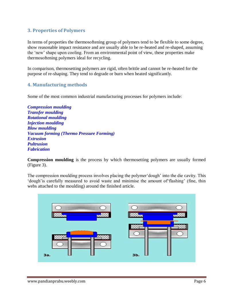
Compression moulding is the process by which thermosetting polymers are usually formed
(Figure 3).
The compression moulding process involves placing the polymer‗dough‘ into the die cavity. This
‗dough‘is carefully measured to avoid waste and minimise the amount of‗flashing‘ (fine, thin
webs attached to the moulding) around the finished article.
Page 7
www.pandianprabu.weebly.com Page 7
Figure 3a. With the dies apart, the prepared polymer ‗dough‘ is placed into the cavity.
Figure 3b. With the die closed, the article is formed and the small amount of flashing on each
side will be removed later.
When the die is closed, heat and pressure is maintained until the condensation polymerisation
process is completed.
The hot compression moulding process is used to form components from phenolic, urea and
melamine thermosetting polymers, as well as alkyd resins.
Transfer moulding is different to compression moulding because the plastic is not fed directly
into the die cavity. Instead it is fed into a chamber outside the die. Here it is preheated before a
piston forces it through a system of runners and gates that allow it into the die cavity. When the
polymer is cured through heat and pressure it is ejected from the mould. The advantage of this
process is that the runner system allows the simultaneous production of many small, intricate
parts and there is no ‗flashing‘ around the finished article.
Rotational moulding is a unique process for manufacturing thermosoftening polymers as it
produces hollow items eg. Lawnmower grass-catchers, balls and some types of children‘s toys. A
split mould is filled with exactly the right quantity of polymer which is then tumbled in the
mould once it is bolted together. The die is rotated in a heated chamber until the polymer is
completely melted. The die is removed from the chamber and continues to rotate until the
polymer is set. The die halves are separated and the article removed.
Injection moulding: In this process thermosoftening polymer powder, or granules, are placed
into a feed hopper connected to a heating chamber. When the fluid state is attained, due to the
heat, a piston or 'screw type' mechanism forces the plastic through a nozzle and into the die.
These are often water-cooled to hasten setting such that when the plastic becomes solid again the
die is opened and the component is ejected. Any flashing is then removed.
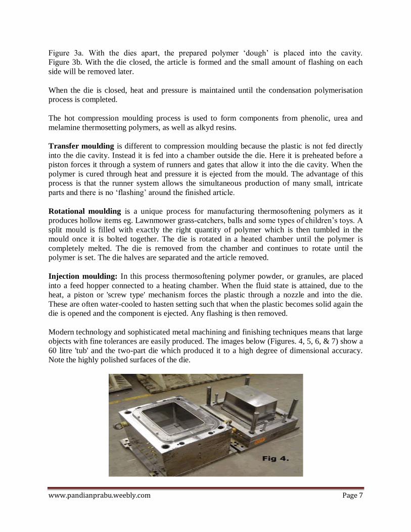
Modern technology and sophisticated metal machining and finishing techniques means that large
objects with fine tolerances are easily produced. The images below (Figures. 4, 5, 6, & 7) show a
60 litre 'tub' and the two-part die which produced it to a high degree of dimensional accuracy.
Note the highly polished surfaces of the die.
Page 8
www.pandianprabu.weebly.com Page 8
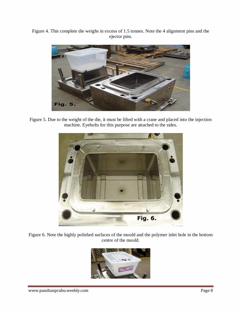
Figure 4. This complete die weighs in excess of 1.5 tonnes. Note the 4 alignment pins and the
ejector pins.
Figure 5. Due to the weight of the die, it must be lifted with a crane and placed into the injection
machine. Eyebolts for this purpose are attached to the sides.
Figure 6. Note the highly polished surfaces of the mould and the polymer inlet hole in the bottom
centre of the mould.
Page 9
www.pandianprabu.weebly.com Page 9
Figure 7. The finished storage 'tub'. The lid is produced inanother mould.
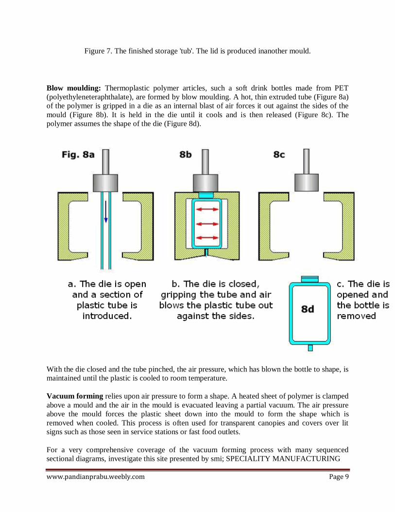
Blow moulding: Thermoplastic polymer articles, such a soft drink bottles made from PET
(polyethyleneteraphthalate), are formed by blow moulding. A hot, thin extruded tube (Figure 8a)
of the polymer is gripped in a die as an internal blast of air forces it out against the sides of the
mould (Figure 8b). It is held in the die until it cools and is then released (Figure 8c). The
polymer assumes the shape of the die (Figure 8d).
With the die closed and the tube pinched, the air pressure, which has blown the bottle to shape, is
maintained until the plastic is cooled to room temperature.
Vacuum forming relies upon air pressure to form a shape. A heated sheet of polymer is clamped
above a mould and the air in the mould is evacuated leaving a partial vacuum. The air pressure
above the mould forces the plastic sheet down into the mould to form the shape which is
removed when cooled. This process is often used for transparent canopies and covers over lit
signs such as those seen in service stations or fast food outlets.
For a very comprehensive coverage of the vacuum forming process with many sequenced
sectional diagrams, investigate this site presented by smi; SPECIALITY MANUFACTURING
Page 10
www.pandianprabu.weebly.com Page 10
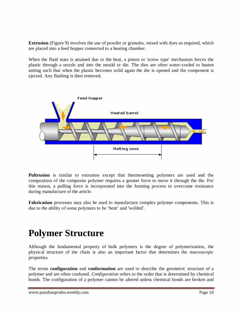
Extrusion (Figure 9) involves the use of powder or granules, mixed with dyes as required, which
are placed into a feed hopper connected to a heating chamber.
When the fluid state is attained due to the heat, a piston or 'screw type' mechanism forces the
plastic through a nozzle and into the mould or die. The dies are often water-cooled to hasten
setting such that when the plastic becomes solid again the die is opened and the component is
ejected. Any flashing is then removed.
Pultrusion is similar to extrusion except that thermosetting polymers are used and the
composition of the composite polymer requires a greater force to move it through the die. For
this reason, a pulling force is incorporated into the forming process to overcome resistance
during manufacture of the article.
Fabrication processes may also be used to manufacture complex polymer components. This is
due to the ability of some polymers to be ‗bent‘ and 'welded'.
Polymer Structure
Although the fundamental property of bulk polymers is the degree of polymerization, the
physical structure of the chain is also an important factor that determines the macroscopic
properties.
The terms configuration and conformation are used to describe the geometric structure of a
polymer and are often confused. Configuration refers to the order that is determined by chemical
bonds. The configuration of a polymer cannot be altered unless chemical bonds are broken and
Page 11
www.pandianprabu.weebly.com Page 11
reformed. Conformation refers to order that arises from the rotation of molecules about the single
bonds. These two structures are studied below.
Configuration
The two types of polymer configurations are cis and trans. These structures can not be changed
by physical means (e.g. rotation). The cis configuration arises when substituent groups are on the
same side of a carbon-carbon double bond. Trans refers to the substituents on opposite sides of
the double bond.
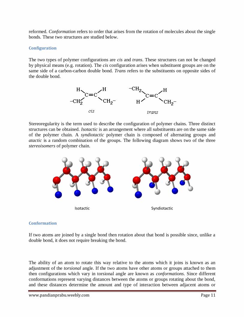
Stereoregularity is the term used to describe the configuration of polymer chains. Three distinct
structures can be obtained. Isotactic is an arrangement where all substituents are on the same side
of the polymer chain. A syndiotactic polymer chain is composed of alternating groups and
atactic is a random combination of the groups. The following diagram shows two of the three
stereoisomers of polymer chain.
Isotactic
Syndiotactic
Conformation
If two atoms are joined by a single bond then rotation about that bond is possible since, unlike a
double bond, it does not require breaking the bond.
The ability of an atom to rotate this way relative to the atoms which it joins is known as an
adjustment of the torsional angle. If the two atoms have other atoms or groups attached to them
then configurations which vary in torsional angle are known as conformations. Since different
conformations represent varying distances between the atoms or groups rotating about the bond,
and these distances determine the amount and type of interaction between adjacent atoms or
Page 12
www.pandianprabu.weebly.com Page 12
groups, different conformation may represent different potential energies of the molecule. There
several possible generalized conformations: Anti (Trans), Eclipsed (Cis), and Gauche (+ or -).
The following animation illustrates the differences between them.
Conformation Lattice Simulation
Like the polymer growth simulation, the conformation lattice simulation takes a statistical
approach to the study of polymers. Probabilities of the different conformations are assigned
which produces a polymer chain with many possible shapes. Click the icon to enter the virtual
laboratory.
Other Chain Structures
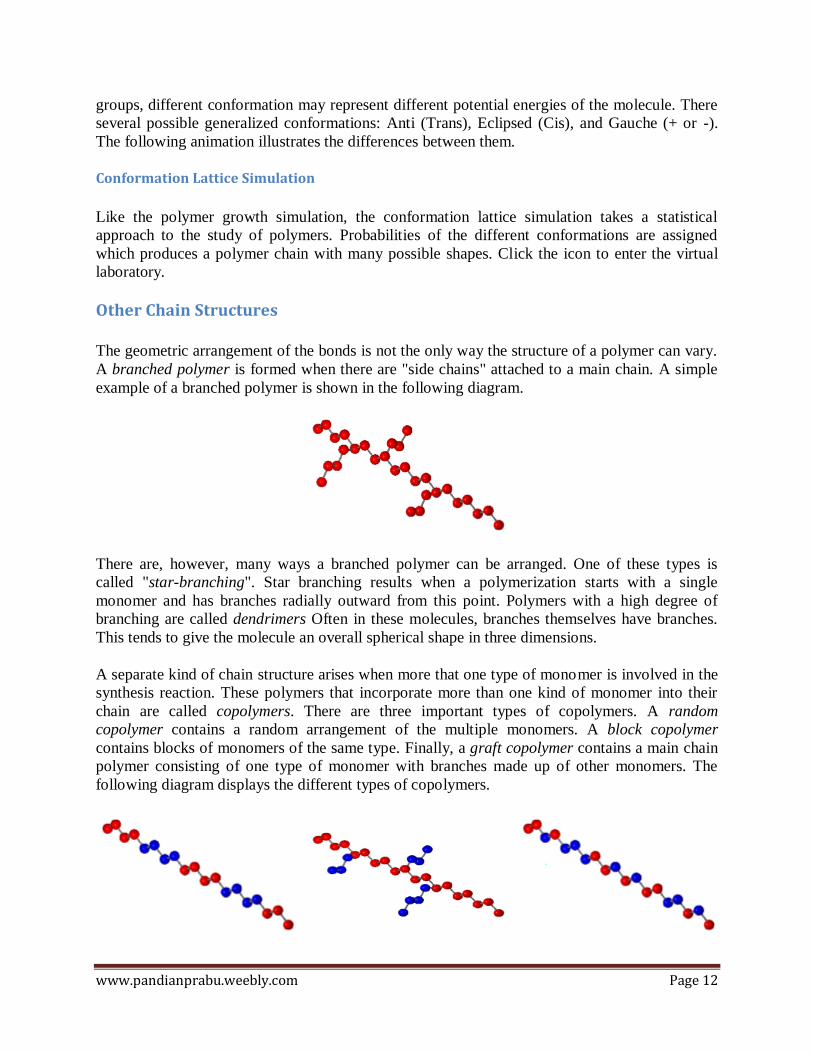
The geometric arrangement of the bonds is not the only way the structure of a polymer can vary.
A branched polymer is formed when there are "side chains" attached to a main chain. A simple
example of a branched polymer is shown in the following diagram.
There are, however, many ways a branched polymer can be arranged. One of these types is
called "star-branching". Star branching results when a polymerization starts with a single
monomer and has branches radially outward from this point. Polymers with a high degree of
branching are called dendrimers Often in these molecules, branches themselves have branches.
This tends to give the molecule an overall spherical shape in three dimensions.
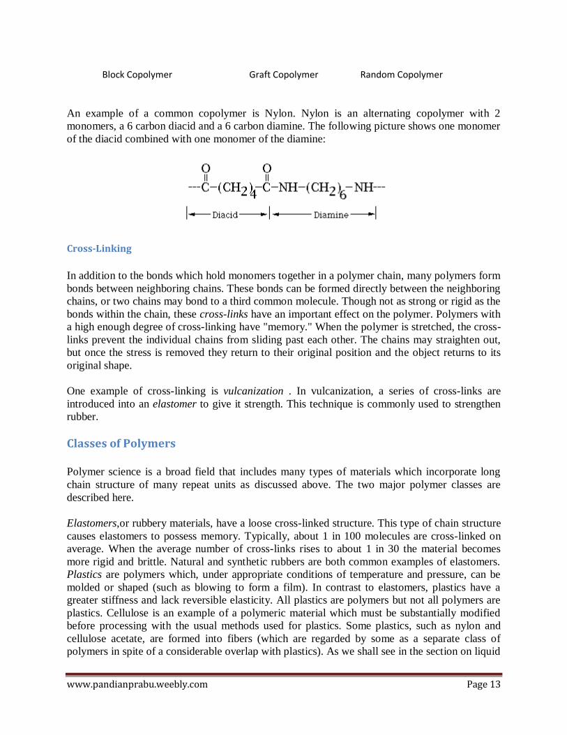
A separate kind of chain structure arises when more that one type of monomer is involved in the
synthesis reaction. These polymers that incorporate more than one kind of monomer into their
chain are called copolymers. There are three important types of copolymers. A random
copolymer contains a random arrangement of the multiple monomers. A block copolymer
contains blocks of monomers of the same type. Finally, a graft copolymer contains a main chain
polymer consisting of one type of monomer with branches made up of other monomers. The
following diagram displays the different types of copolymers.
Page 13
www.pandianprabu.weebly.com Page 13
Block Copolymer
Graft Copolymer Random Copolymer
An example of a common copolymer is Nylon. Nylon is an alternating copolymer with 2
monomers, a 6 carbon diacid and a 6 carbon diamine. The following picture shows one monomer
of the diacid combined with one monomer of the diamine:
Cross-Linking
In addition to the bonds which hold monomers together in a polymer chain, many polymers form
bonds between neighboring chains. These bonds can be formed directly between the neighboring
chains, or two chains may bond to a third common molecule. Though not as strong or rigid as the
bonds within the chain, these cross-links have an important effect on the polymer. Polymers with
a high enough degree of cross-linking have "memory." When the polymer is stretched, the cross-
links prevent the individual chains from sliding past each other. The chains may straighten out,
but once the stress is removed they return to their original position and the object returns to its
original shape.
One example of cross-linking is vulcanization . In vulcanization, a series of cross-links are
introduced into an elastomer to give it strength. This technique is commonly used to strengthen
rubber.
Classes of Polymers
Polymer science is a broad field that includes many types of materials which incorporate long
chain structure of many repeat units as discussed above. The two major polymer classes are
described here.
Elastomers,or rubbery materials, have a loose cross-linked structure. This type of chain structure
causes elastomers to possess memory. Typically, about 1 in 100 molecules are cross-linked on
average. When the average number of cross-links rises to about 1 in 30 the material becomes
more rigid and brittle. Natural and synthetic rubbers are both common examples of elastomers.
Plastics are polymers which, under appropriate conditions of temperature and pressure, can be
molded or shaped (such as blowing to form a film). In contrast to elastomers, plastics have a
greater stiffness and lack reversible elasticity. All plastics are polymers but not all polymers are
plastics. Cellulose is an example of a polymeric material which must be substantially modified
before processing with the usual methods used for plastics. Some plastics, such as nylon and
cellulose acetate, are formed into fibers (which are regarded by some as a separate class of
polymers in spite of a considerable overlap with plastics). As we shall see in the section on liquid
Page 14
www.pandianprabu.weebly.com Page 14
crystals, some of the main chain polymer liquid crystals also are the constituents of important
fibers. Every day plastics such as polyethylene and poly(vinyl chloride) have replaced traditional
materials like paper and copper for a wide variety of applications. The section on Polymer
Applications will go into greater detail about the special properties of the many types of
polymers.
Fiber Manufacturing Technology
Synthetic and Cellulosic Fiber Formation Technology
Most synthetic and cellulosic manufactured fibers are created by ―extrusion‖ — forcing a thick,
viscous liquid (about the consistency of cold honey) through the tiny holes of a device called a
spinneret to form continuous filaments of semi-solid polymer.
In their initial state, the fiber-forming polymers are solids and therefore must be first converted
into a fluid state for extrusion. This is usually achieved by melting, if the polymers are
thermoplastic synthetics (i.e., they soften and melt when heated), or by dissolving them in a
suitable solvent if they are non-thermoplastic cellulosics. If they cannot be dissolved or melted
directly, they must be chemically treated to form soluble or thermoplastic derivatives. Recent
technologies have been developed for some specialty fibers made of polymers that do not melt,
dissolve, or form appropriate derivatives. For these materials, the small fluid molecules are
mixed and reacted to form the otherwise intractable polymers during the extrusion process.
The Spinneret
The spinnerets used in the production of most manufactured fibers are similar, in principle, to a
bathroom shower head. A spinneret may have from one to several hundred holes. The tiny
openings are very sensitive to impurities and corrosion. The liquid feeding them must be
carefully filtered (not an easy task with very viscous materials) and, in some cases, the spinneret
must be made from very expensive, corrosion-resistant metals. Maintenance is also critical, and
spinnerets must be removed and cleaned on a regular basis to prevent clogging.
As the filaments emerge from the holes in the spinneret, the liquid polymer is converted first to a
rubbery state and then solidified. This process of extrusion and solidification of endless filaments
is called spinning, not to be confused with the textile operation of the same name, where short
pieces of staple fiber are twisted into yarn. There are four methods of spinning filaments of
manufactured fibers: wet, dry, melt, and gel spinning.
Page 15
www.pandianprabu.weebly.com Page 15
Wet Spinning Wet spinning is the oldest process. It is used for fiber-forming
substances that have been dissolved in a solvent. The spinnerets
are submerged in a chemical bath and as the filaments emerge
they precipitate from solution and solidify.
Because the solution is extruded directly into the precipitating
liquid, this process for making fibers is called wet spinning.
Acrylic, rayon, aramid, modacrylic and spandex can be
produced by this process.
Dry Spinning
Dry spinning is also used for fiber-forming substances in
solution. However, instead of precipitating the polymer by
dilution or chemical reaction, solidification is achieved by
evaporating the solvent in a stream of air or inert gas.
The filaments do not come in contact with a precipitating
liquid, eliminating the need for drying and easing solvent
recovery. This process may be used
for the production of acetate,
triacetate, acrylic, modacrylic, PBI,
spandex, and vinyon.
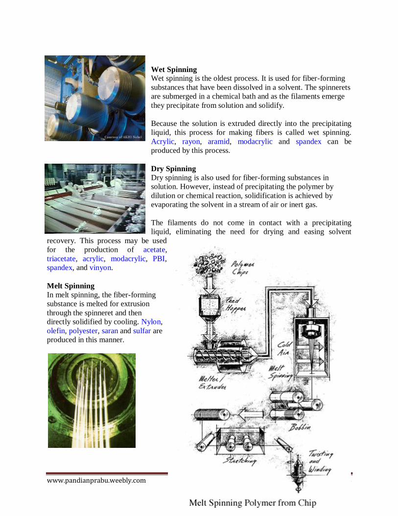
Melt Spinning
In melt spinning, the fiber-forming
substance is melted for extrusion
through the spinneret and then
directly solidified by cooling. Nylon,
olefin, polyester, saran and sulfar are
produced in this manner.
Page 16
www.pandianprabu.weebly.com Page 16
Melt spun fibers can be extruded from the spinneret in different cross-sectional shapes (round,
trilobal, pentagonal, octagonal, and others). Trilobal-shaped fibers reflect more light and give an
attractive sparkle to textiles.
Pentagonal-shaped and hollow fibers, when used in carpet, show less soil and dirt. Octagonal-
shaped fibers offer glitter-free effects. Hollow fibers trap air, creating insulation and provide loft
characteristics equal to, or better than, down.
Gel Spinning
Gel spinning is a special process used to obtain high strength or other special fiber properties.
The polymer is not in a true liquid state during extrusion. Not completely separated, as they
would be in a true solution, the polymer chains are bound together at various points in liquid
crystal form. This produces strong inter-chain forces in the resulting filaments that can
significantly increase the tensile strength of the fibers. In addition, the liquid crystals are aligned
along the fiber axis by the shear forces during extrusion. The filaments emerge with an unusually
high degree of orientation relative to each other, further enhancing strength. The process can also
be described as dry-wet spinning, since the filaments first pass through air and then are cooled
further in a liquid bath. Some high-strength polyethylene and aramid fibers are produced by gel
spinning.
Stretching and Orientation While extruded fibers are solidifying, or in some cases even after they have hardened, the
filaments may be drawn to impart strength. Drawing pulls the molecular chains together and
orients them along the fiber axis, creating a considerably stronger yarn.
FOAM MANUFACTURING
Polystyrene Foam
o Polystyrene foam, often known as Styrofoam, is made from petroleum by-products
called styrenes. The process of turning styrenes into foam is known as
polymerization. First the styrene is infused with hydrocarbon gas, which causes the
molecules to expand. The hydrocarbon-infused styrene is then heated to further
expand each molecule, then placed in a mold. The mold is heated with steam to
cause the styrene to take the shape of the mold once it is released. This process is
used to produced packing foam and building insulation. The resulting foam
material is often known as expanded polystyrene (EPS) and is commonly called
"beadboard."
Page 17
www.pandianprabu.weebly.com Page 17
Polyurethane Foam
o Polyurethane foam is manufactured from man-made particles called polymers. The
polymers are joined by urethanes, or carbamates, and stored as a liquid in large
vats. The vats are continuously agitated to keep the solution mixed and ready for
production. To produce polyurethane foam, the liquid is heated and pumped into a
series of pipes, where it is sprayed out onto sheets of heavy paper. Once it has
been sprayed, it is infused with carbon dioxide gas, which causes it to rise like
bread dough. Additional sheets of paper are added to form the foam into the
desired shape, and it is then cooled and cut to the desired length. Polyurethane
foam is often found in mattresses and other furnishings, and rigid units are used in
flower arrangements.
Polyethylene Foam
o Polyethylene foam is an extruded product made from a thermoplastic compound
called ethene. The liquid ethene is heated and drawn through a series of molds or
dies to create the desired shape. Large sheets of ethene are called "buns," and may
be placed into molds and heated to form a variety of products. Soft polyethylene
foam us used as padding in shoes and carpeting, while rigid versions are often used
in sculpture or insulation.
Adhesive manufacturing
An adhesive, also known as glue, is a material, typically liquid or semi-liquid, that adheres or
bonds items together. Adhesives come from either natural or synthetic sources. The types of
materials that can be bonded are vast but adhesives are especially useful for bonding thin
materials. Adhesives cure (harden) by either evaporating a solvent or by chemical reactions that
occur between two or more constituents.
Adhesives are also very useful for joining thin or dissimilar materials, minimizing weight, and
providing a vibration-damping joint. A disadvantage of most adhesives is that most do not form
an instantaneous joint, unlike many other joining processes, because the adhesive needs time to
cure.
Page 18
www.pandianprabu.weebly.com Page 18
Economic importance
In the course of time and during their development, adhesives have gained a stable position in an
increasing number of production processes. There is hardly any product in our surroundings that
does not contain at least one adhesive – be it the label on a beverage bottle, protective coatings
on automobiles or profiles on window frames. Market researchers forecast a turnover of almost
US$50 billion for the global adhesives market in 2019. Especially the dynamic economic
development in emerging countries such as China, India, Russia or Brazil will cause a rising
demand for adhesives in the future.
Types
Adhesives are typically organized by the method of adhesion. These are then organized into
reactive and non-reactive adhesives, which refers to if the adhesive chemically reacts to harden.
Alternatively they can be organized by whether the raw stock is of natural, or synthetic origin, or
by their starting physical phase.
Non-reactive adhesives
Drying adhesives
There are two types of adhesives that harden by drying: solvent based adhesives and polymer
dispersion adhesives, also known as emulsion adhesives. Solvent based adhesives are a mixture
of ingredients (typically polymers) dissolved in a solvent. White glue, contact adhesives and
rubber cements are members of the drying adhesive family. As the solvent evaporates, the
adhesive hardens. Depending on the chemical composition of the adhesive, they will adhere to
different materials to greater or lesser degrees.
Polymer dispersion adhesives are milky-white dispersions often based on polyvinyl acetate
(PVAc). They are used extensively in the woodworking and packaging industries; also used with
fabrics and fabric-based components, and in engineered products such as loudspeaker cones.
Pressure sensitive adhesives
Pressure sensitive adhesives (PSA) form a bond by the application of light pressure to marry the
adhesive with the adherend. They are designed with a balance between flow and resistance to
flow. The bond forms because the adhesive is soft enough to flow (i.e. "wet") to the adherend.
The bond has strength because the adhesive is hard enough to resist flow when stress is applied
to the bond. Once the adhesive and the adherend are in close proximity, molecular interactions,
such as van der Waals forces, become involved in the bond, contributing significantly to its
ultimate strength.
PSAs are designed for either permanent or removable applications. Examples of permanent
applications include safety labels for power equipment, foil tape for HVAC duct work,
automotive interior trim assembly, and sound/vibration damping films. Some high performance
permanent PSAs exhibit high adhesion values and can support kilograms of weight per square
Page 19
www.pandianprabu.weebly.com Page 19
centimeter of contact area, even at elevated temperature. Permanent PSAs may be initially
removable (for example to recover mislabeled goods) and build adhesion to a permanent bond
after several hours or days.
Removable adhesives are designed to form a temporary bond, and ideally can be removed after
months or years without leaving residue on the adherend. Removable adhesives are used in
applications such as surface protection films, masking tapes, bookmark and note papers, price
marking labels, promotional graphics materials, and for skin contact (wound care dressings,
EKG electrodes, athletic tape, analgesic and transdermal drug patches, etc.). Some removable
adhesives are designed to repeatedly stick and unstick. They have low adhesion and generally
can not support much weight.
Pressure sensitive adhesives are manufactured with either a liquid carrier or in 100% solid form.
Articles are made from liquid PSAs by coating the adhesive and drying off the solvent or water
carrier. They may be further heated to initiate a cross-linking reaction and increase molecular
weight. 100% solid PSAs may be low viscosity polymers that are coated and then reacted with
radiation to increase molecular weight and form the adhesive; or they may be high viscosity
materials that are heated to reduce viscosity enough to allow coating, and then cooled to their
final form. Major raw material for PSA's are acrylate based polymers.
Contact adhesives
Contact adhesives are used in strong bonds with high shear-resistance like laminates, such as
bonding Formica to a wooden counter, and in footwear, as in attaching outsoles to uppers.
Natural rubber and polychloroprene (Neoprene) are commonly used contact adhesives. Both of
these elastomers undergo strain crystallization. In the construction industry a specialised
proprietary adhesive known as Liquid Nails (or liquid nails as the generic), is used. This also
copes with tasks such as sealing artificial turf.
Contact adhesives must be applied to both surfaces and allowed some time to dry before the two
surfaces are pushed together. Some contact adhesives require as long as 24 hours to dry before
the surfaces are to be held together. Once the surfaces are pushed together, the bond forms very
quickly. It is usually not necessary to apply pressure for a long time, so there is less need for
clamps.
Hot adhesives
Hot adhesives, also known as hot melt adhesives, are thermoplastics applied in molten form (in
the 65-180 °C range) which solidify on cooling to form strong bonds between a wide range of
materials. Ethylene-vinyl acetate based hot-melts are particularly popular for crafts because of
their ease of use and the wide range of common materials they can join. A glue gun (shown at
right) is one method of applying hot adhesives. The glue gun melts the solid adhesive then
allows the liquid to pass through its barrel onto the material, where it solidifies.
Page 20
www.pandianprabu.weebly.com Page 20
Thermoplastic glue may have been invented around 1940 by Procter & Gamble as a solution to
water-based adhesives commonly used in packaging at that time failing in humid climates,
causing packages to open.
Reactive adhesives
Multi-part adhesives
Multi-component adhesives harden by mixing two or more components which chemically react.
This reaction causes polymers to cross-link into acrylics, urethanes, and epoxies.
There are several commercial combinations of multi-component adhesives in use in industry.
Some of these combinations are:
Polyester resin – polyurethane resin Polyols – polyurethane resin Acrylic polymers – polyurethane resins
The individual components of a multi-component adhesive are not adhesive by nature. The
individual components react with each other after being mixed and show full adhesion only on
curing. The multi-component resins can be either solvent-based or solvent-less. The solvents
present in the adhesives are a medium for the polyester or the polyurethane resin. The solvent is
dried during the curing process.
One-part adhesives
One-part adhesives harden via a chemical reaction with an external energy source, such as
radiation, heat, and moisture.
Ultraviolet (UV) light curing adhesives, also known as light curing materials (LCM), have
become popular within the manufacturing sector due to their rapid curing time and strong bond
strength. Light curing adhesives can cure in as little as a second and many formulations can bond
dissimilar substrates (materials) and withstand harsh temperatures. These qualities make UV
curing adhesives essential to the manufacturing of items in many industrial markets such as
electronics, telecommunications, medical, aerospace, glass, and optical. Unlike traditional
adhesives, UV light curing adhesives not only bond materials together but they can also be used
to seal and coat products. They are generally acrylic based.
Heat curing adhesives consist of a pre-made mixture of two or more components. When heat is
applied the components react and cross-link. This type of adhesive includes epoxies, urethanes,
and polyimides.
Moisture curing adhesives cure when they react with moisture present on the substrate surface or
in the air. This type of adhesive includes cyanoacrylates and urethanes.
Page 21
www.pandianprabu.weebly.com Page 21
Natural adhesives
Natural adhesives are made from organic sources such as vegetable matter, starch (dextrin),
natural resins or from animals e.g. casein or animal glue. They are often referred to as
bioadhesives. One example is a simple paste made by cooking flour in water. Animal glues are
traditionally used in bookbinding, wood joining, and many other areas but now are largely
replaced by synthetic glues. Casein is mainly used to adhere glass bottle labels. Starch based
adhesives are used in corrugated board production and paper sack production, paper tube
winding, and wall paper adhesives. Masonite, a wood hardboard, was bonded using natural
lignin, (although most modern MDF particle boards use synthetic thermosetting resins). Another
form of natural adhesive is blood albumen (made from protein component of blood), which is
used in the plywood industry. Animal glue remains the preferred glue of the luthier. Casein
based glues are made by precipitating casein from milk protein using the acetic acid from
vinegar. This forms curds, which are neutralized with a base, such as sodium bicarbonate (baking
soda), to cause them to unclump and become a thicker plastic-like substance.
Synthetic adhesives
Synthetic adhesives are based on elastomers, thermoplastics, emulsions, and thermosets.
Examples of thermosetting adhesives are: epoxy, polyurethane, cyanoacrylate and acrylic
polymers. See also post-it notes. The first commercially produced synthetic adhesive was
Karlsons klister in the 1920s.
Application
Applicators of different adhesives are designed according to the adhesive being used and the size
of the area to which the adhesive will be applied. The adhesive is applied to either one or both of
the materials being bonded. The pieces are aligned and pressure is added to aid in adhesion and
rid the bond of air bubbles.
Common ways of applying an adhesive include brushes, rollers, using films or pellets, spray
guns and applicator guns (e.g., caulk gun). All of these can be done manually or can be
automated into a machine.
Mechanisms of adhesion
Adhesion, the attachment between adhesive and substrate may occur either by mechanical
means, in which the adhesive works its way into small pores of the substrate, or by one of several
chemical mechanisms. The strength of adhesion depends on many factors, including the means
by which it occurs.
In some cases, an actual chemical bond occurs between adhesive and substrate. In others,
electrostatic forces, as in static electricity, hold the substances together. A third mechanism
involves the van der Waals forces that develop between molecules. A fourth means involves the
moisture-aided diffusion of the glue into the substrate, followed by hardening.
Page 22
www.pandianprabu.weebly.com Page 22
Failure of the adhesive joint
There are several factors that could contribute to the failure of two adhered surfaces. Sunlight
and heat may weaken the adhesive. Solvents can deteriorate or dissolve adhesive. Physical
stresses may also cause the separation of surfaces. When subjected to loading, debonding may
occur at different locations in the adhesive joint. The major fracture types are the following:
Cohesive fracture
Cohesive fracture is obtained if a crack propagates in the bulk polymer which constitutes the
adhesive. In this case the surfaces of both adherents after debonding will be covered by fractured
adhesive. The crack may propagate in the center of the layer or near an interface. For this last
case, the cohesive fracture can be said to be ―cohesive near the interface‖.
Interfacial fracture
The fracture is adhesive or interfacial when debonding occurs between the adhesive and the
adherent. In most cases, the occurrence of interfacial fracture for a given adhesive goes along
with a smaller fracture toughness. The interfacial character of a fracture surface is usually to
identify the precise location of the crack path in the interphase.
Other types of fracture
Other types of fracture include:
The mixed type, which occurs if the crack propagates at some spots in a cohesive and in others in an interfacial manner. Mixed fracture surfaces can be characterised by a certain percentage of adhesive and cohesive areas.
Page 23
www.pandianprabu.weebly.com Page 23
The alternating crack path type which occurs if the cracks jump from one interface to the other. This type of fracture appears in the presence of tensile pre-stresses in the adhesive layer.
Fracture can also occur in the adherent if the adhesive is tougher than the adherent. In this case, the adhesive remains intact and is still bonded to one substrate and remnants of the other. For example, when one removes a price label, the adhesive usually remains on the label and the surface. This is cohesive failure. If, however, a layer of paper remains stuck to the surface, the adhesive has not failed. Another example is when someone tries to pull apart Oreo cookies and all the filling remains on one side; this is an adhesive failure, rather than a cohesive failure.
Design of adhesive joints
As a general design rule, the material properties of the object need to be greater than the forces
anticipated during its use. (i.e. geometry, loads, etc.). The engineering work will consist of
having a good model to evaluate the function. For most adhesive joints, this can be achieved
using fracture mechanics. Concepts such as the stress concentration factor and the strain energy
release rate can be used to predict failure. In such models, the behavior of the adhesive layer
itself is neglected and only the adherents are considered.
Failure will also very much depend on the opening mode of the joint.
Mode I is an opening or tensile mode where the loadings are normal to the crack. Mode II is a sliding or in-plane shear mode where the crack surfaces slide over one another in
direction perpendicular to the leading edge of the crack. This is typically the mode for which the adhesive exhibits the highest resistance to fracture.
Mode III is a tearing or antiplane shear mode.
As the loads are usually fixed, an acceptable design will result from combination of a material
selection procedure and geometry modifications, if possible. In adhesively bonded structures, the
global geometry and loads are fixed by structural considerations and the design procedure
focuses on the material properties of the adhesive and on local changes on the geometry.
Increasing the joint resistance is usually obtained by designing its geometry so that:
The bonded zone is large It is mainly loaded in mode II Stable crack propagation will follow the appearance of a local failure.
Page 24
www.pandianprabu.weebly.com Page 24
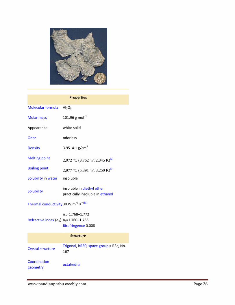
Alumina (Al2O3) - Properties and
Applications by Precision Ceramics
Topics Covered
Characteristics of Alumina and Aluminium Oxide
Properties of Aluminium Oxide
Corrosion Resistance of Aluminium Oxide
Applications of Aluminium Oxide
Alumina Bead as Electrical Insulators
Characteristics of Alumina and Aluminium Oxide
Alumina is the more common name of Aluminium Oxide (Al2O3) and is a hard wearing material
used for many applications. Once fired and sintered, it can only be machined using diamond-
grinding methods.
Aluminium oxide is an electrical insulator but has a relatively high thermal conductivity (40
W/m K). In its most commonly occurring crystalline form, called corundum or á-aluminium
oxide, its hardness makes it suitable for use as an abrasive and as a component in cutting tools.
Properties of Aluminium Oxide
Aluminium oxide is responsible for metallic aluminium's resistance to weathering. Metallic
aluminium is very reactive with atmospheric oxygen, and a thin passivation layer of alumina
quickly forms on any exposed aluminium surface. This layer protects the metal from further
oxidation. The thickness and properties of this oxide layer can be enhanced using a process
called anodising.
Corrosion Resistance of Aluminium Oxide
A number of alloys, such as aluminium bronzes, exploit this property by including a proportion
of aluminium in the alloy to enhance corrosion resistance. The alumina generated by anodising is
typically amorphous, but discharge assisted oxidation processes such as plasma electrolytic
oxidation result in a significant proportion of crystalline alumina in the coating, enhancing its
hardness.
Applications of Aluminium Oxide
Alumina's combination of hardness, high temperature operation and good electrical insulation
makes it useful for a wide range of applications. Alumina is the most commonly used type of
Page 25
www.pandianprabu.weebly.com Page 25
ceramic and is available in purities up to 99.9%. Typical applications inlcude electrical
insulators; seal faces; valve seats.
Alumina Bead as Electrical Insulators
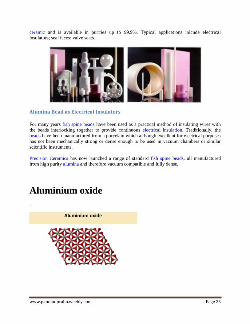
For many years fish spine beads have been used as a practical method of insulating wires with
the beads interlocking together to provide continuous electrical insulation. Traditionally, the
beads have been manufactured from a porcelain which although excellent for electrical purposes
has not been mechanically strong or dense enough to be used in vacuum chambers or similar
scientific instruments.
Precision Ceramics has now launched a range of standard fish spine beads, all manufactured
from high purity alumina and therefore vacuum compatible and fully dense.
Aluminium oxide
.
Aluminium oxide
Page 26
www.pandianprabu.weebly.com Page 26
Properties
Molecular formula Al2O3
Molar mass 101.96 g mol−1
Appearance white solid
Odor odorless
Density 3.95–4.1 g/cm3
Melting point
2,072 °C (3,762 °F; 2,345 K)[2]
Boiling point
2,977 °C (5,391 °F; 3,250 K)[3]
Solubility in water insoluble
Solubility
insoluble in diethyl ether
practically insoluble in ethanol
Thermal conductivity 30 W·m−1·K−1[1]
Refractive index (nD)
nω=1.768–1.772
nε=1.760–1.763
Birefringence 0.008
Structure
Crystal structure
Trigonal, hR30, space group = R3c, No.
167
Coordination
geometry
octahedral
Page 27
www.pandianprabu.weebly.com Page 27
Thermochemistry
Std enthalpy of
formation ΔfHo
298 −1675.7 kJ·mol−1[4]
Standard molar
entropy So298
50.92 J·mol−1·K−1[4]
Hazards
MSDS External MSDS
EU classification Not listed.
NFPA 704
0
1
0
Flash point non-flammable
Related compounds
Other anions aluminium hydroxide
Other cations
boron trioxide
gallium oxide
indium oxide
thallium oxide
Supplementary data page
Structure and
properties
n, εr, etc.
Thermodynamic
data
Phase behaviour
Solid, liquid, gas
Spectral data UV, IR, NMR, MS
Page 28
www.pandianprabu.weebly.com Page 28
Aluminium oxide is a chemical compound of aluminium and oxygen with the chemical formula
Al2O3. It is the most commonly occurring of several aluminium oxides, and specifically
identified as aluminium(III) oxide. It is commonly called alumina, and may also be called
aloxide, aloxite, or alundum depending on particular forms or applications. It commonly occurs
in its crystalline polymorphic phase α-Al2O3, in which it comprises the mineral corundum,
varieties of which form the precious gems ruby and sapphire. Al2O3 is significant in its use to
produce aluminium metal, as an abrasive owing to its hardness, and as a refractory material
owing to its high melting point
Natural occurrence
Corundum is the most common naturally occurring crystalline form of aluminium oxide. Rubies
and sapphires are gem-quality forms of corundum, which owe their characteristic colors to trace
impurities. Rubies are given their characteristic deep red color and their laser qualities by traces
of chromium. Sapphires come in different colors given by various other impurities, such as iron
and titanium.
Properties
Al2O3 is an electrical insulator but has a relatively high thermal conductivity (30 Wm−1
K−1[1]
) for
a ceramic material. In its most commonly occurring crystalline form, called corundum or α-
aluminium oxide, its hardness makes it suitable for use as an abrasive and as a component in
cutting tools.
Aluminium oxide is responsible for the resistance of metallic aluminium to weathering. Metallic
aluminium is very reactive with atmospheric oxygen, and a thin passivation layer of aluminium
oxide (4 nm thickness) forms on any exposed aluminium surface.[6]
This layer protects the metal
from further oxidation. The thickness and properties of this oxide layer can be enhanced using a
process called anodising. A number of alloys, such as aluminium bronzes, exploit this property
by including a proportion of aluminium in the alloy to enhance corrosion resistance. The
aluminium oxide generated by anodising is typically amorphous, but discharge assisted oxidation
processes such as plasma electrolytic oxidation result in a significant proportion of crystalline
aluminium oxide in the coating, enhancing its hardness.
Aluminium oxide is completely insoluble in water. However it is an amphoteric substance,
meaning it can react with both acids and bases, such as hydrochloric acid and sodium hydroxide.
Al2O3 + 6 HCl → 2 AlCl3 + 3 H2O
Al2O3 + 6 NaOH + 3 H2O → 2 Na3Al(OH)6
Aluminium oxide was taken off the United States Environmental Protection Agency's chemicals
lists in 1988. Aluminium oxide is on EPA's Toxics Release Inventory list if it is a fibrous form.
Page 29
www.pandianprabu.weebly.com Page 29
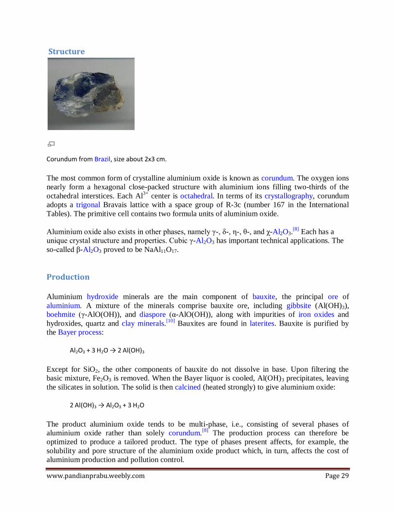
Structure
Corundum from Brazil, size about 2x3 cm.
The most common form of crystalline aluminium oxide is known as corundum. The oxygen ions
nearly form a hexagonal close-packed structure with aluminium ions filling two-thirds of the
octahedral interstices. Each Al3+
center is octahedral. In terms of its crystallography, corundum
adopts a trigonal Bravais lattice with a space group of R-3c (number 167 in the International
Tables). The primitive cell contains two formula units of aluminium oxide.
Aluminium oxide also exists in other phases, namely γ-, δ-, η-, θ-, and χ-Al2O3.[8]
Each has a
unique crystal structure and properties. Cubic γ-Al2O3 has important technical applications. The
so-called β-Al2O3 proved to be NaAl11O17.
Production
Aluminium hydroxide minerals are the main component of bauxite, the principal ore of
aluminium. A mixture of the minerals comprise bauxite ore, including gibbsite (Al(OH)3),
boehmite (γ-AlO(OH)), and diaspore (α-AlO(OH)), along with impurities of iron oxides and
hydroxides, quartz and clay minerals.[10]
Bauxites are found in laterites. Bauxite is purified by
the Bayer process:
Al2O3 + 3 H2O → 2 Al(OH)3
Except for SiO2, the other components of bauxite do not dissolve in base. Upon filtering the
basic mixture, Fe2O3 is removed. When the Bayer liquor is cooled, Al(OH)3 precipitates, leaving
the silicates in solution. The solid is then calcined (heated strongly) to give aluminium oxide:
2 Al(OH)3 → Al2O3 + 3 H2O
The product aluminium oxide tends to be multi-phase, i.e., consisting of several phases of
aluminium oxide rather than solely corundum.[8]
The production process can therefore be
optimized to produce a tailored product. The type of phases present affects, for example, the
solubility and pore structure of the aluminium oxide product which, in turn, affects the cost of
aluminium production and pollution control.
Page 30
www.pandianprabu.weebly.com Page 30
Known as alundum (in fused form) or aloxite[11]
in the mining, ceramic, and materials science
communities, aluminium oxide finds wide use. Annual world production of aluminium oxide is
approximately 45 million tonnes, over 90% of which is used in the manufacture of aluminium
metal.[5]
The major uses of specialty aluminium oxides are in refractories, ceramics, and
polishing and abrasive applications. Large tonnages are also used in the manufacture of zeolites,
coating titania pigments, and as a fire retardant/smoke suppressant.
Applications
The great majority of aluminium oxide is consumed for the production of aluminium, usually by
the Hall process.
Filler
Being fairly chemically inert and white, aluminium oxide is a favored filler for plastics.
Aluminium oxide is a common ingredient in sunscreen and is sometimes present in cosmetics
such as blush, lipstick, and nail polish.
Catalysis
Aluminium oxide catalyses a variety of reactions that are useful industrially. In its largest scale
application, aluminium oxide is the catalyst in the Claus process for converting hydrogen sulfide
waste gases into elemental sulfur in refineries. It is also useful for dehydration of alcohols to
alkenes.
Aluminium oxide serves as a catalyst support for many industrial catalysts, such as those used in
hydrodesulfurization and some Ziegler-Natta polymerizations.
Purification
Aluminium oxide is widely used to remove water from gas streams. Other major applications are
described below.
Abrasive
Aluminium oxide is used for its hardness and strength. It is widely used as an abrasive, including
as a much less expensive substitute for industrial diamond. Many types of sandpaper use
aluminium oxide crystals. In addition, its low heat retention and low specific heat make it widely
used in grinding operations, particularly cutoff tools. As the powdery abrasive mineral aloxite, it
is a major component, along with silica, of the cue tip "chalk" used in billiards. Aluminium oxide
powder is used in some CD/DVD polishing and scratch-repair kits. Its polishing qualities are
also behind its use in toothpaste. Aluminium oxide can be grown as a coating on aluminium by
anodising or by plasma electrolytic oxidation (see the "Properties" above). Both its strength and
abrasive characteristics originate from the high hardness (9 on the Mohs scale of mineral
hardness) of aluminium oxide.
Page 31
www.pandianprabu.weebly.com Page 31
Paint
Template:Main:Alumina effect pigment Aluminium oxide flakes are used in paint for reflective
decorative effects, such as in the automotive or cosmetic industries.
Composite fiber
Aluminium oxide has been used in a few experimental and commercial fiber materials for high-
performance applications (e.g., Fiber FP, Nextel 610, Nextel 720).
Other
In lighting, transparent aluminium oxide is used in some sodium vapor lamps. Aluminium oxide
is also used in preparation of coating suspensions in compact fluorescent lamps.
In chemistry laboratories, aluminium oxide is a medium for chromatography, available in basic
(pH 9.5), acidic (pH 4.5 when in water) and neutral formulations.
Health and medical applications include it as a material in hip replacements.[5]
As well, it is used as a dosimeter for radiation protection and therapy applications for its
optically stimulated luminescence properties.
Aluminium oxide is an electrical insulator used as a substrate (Silicon on sapphire) for integrated
circuits but also as a tunnel barrier for the fabrication of superconducting devices such as single
electron transistors and superconducting quantum interference (SQUID) devices.
Insulation for high-temperature furnaces is often manufactured from aluminium oxide.
Sometimes the insulation has varying percentages of silica depending on the temperature rating
of the material. The insulation can be made in blanket, board, brick and loose fiber forms for
various application requirements.
Small pieces of aluminium oxide are often used as boiling chips in chemistry.
It is also used to make spark plug insulators.
Using a plasma spray process and mixed with titania, it is coated onto the braking surface of
some aluminium bicycle rims to provide abrasion and wear resistance.[citation neede
Aluminum Oxide, Al2O3 Material Characteristics
Alumina is the most cost effective and widely used material in the family of engineering
ceramics. The raw materials from which this high performance technical grade ceramic is made
Page 32
www.pandianprabu.weebly.com Page 32
are readily available and reasonably priced, resulting in good value for the cost in fabricated
alumina shapes. With an excellent combination of properties and an attractive price, it is no
surprise that fine grain technical grade alumina has a very wide range of applications.
.Key Properties
Hard, wear-resistant
Excellent dielectric properties from DC to GHz frequencies
Resists strong acid and alkali attack at elevated temperatures
Good thermal conductivity
Excellent size and shape capability
High strength and stiffness
Available in purity ranges from 94%, an easily metallizable composition, to 99.5% for the most
demanding high temperature applications.
.
Typical Uses
Gas laser tubes
Wear pads
Seal rings
High temperature electrical insulators
High voltage insulators
Furnace liner tubes
Thread and wire guides
Electronic substrates
Ballistic armor
Abrasion resistant tube and elbow liners
Thermometry sensors
Page 33
www.pandianprabu.weebly.com Page 33
Laboratory instrument tubes and sample holders
Instrumentation parts for thermal property test machines
Grinding media
General Information
Aluminum oxide, commonly referred to as alumina, possesses strong ionic interatomic bonding
giving rise to it‘s desirable material characteristics. It can exist in several crystalline phases
which all revert to the most stable hexagonal alpha phase at elevated temperatures. This is the
phase of particular interest for structural applications and the material available from Accuratus.
Alpha phase alumina is the strongest and stiffest of the oxide ceramics. Its high hardness,
excellent dielectric properties, refractoriness and good thermal properties make it the material of
choice for a wide range of applications.
High purity alumina is usable in both oxidizing and reducing atmospheres to 1925°C. Weight
loss in vacuum ranges from 10–7
to 10–6
g/cm2.sec over a temperature range of 1700° to 2000°C.
It resists attack by all gases except wet fluorine and is resistant to all common reagents except
hydrofluoric acid and phosphoric acid. Elevated temperature attack occurs in the presence of
alkali metal vapors particularly at lower purity levels.
The composition of the ceramic body can be changed to enhance particular desirable material
characteristics. An example would be additions of chrome oxide or manganese oxide to improve
hardness and change color. Other additions can be made to improve the ease and consistency of
metal films fired to the ceramic for subsequent brazed and soldered assembly.
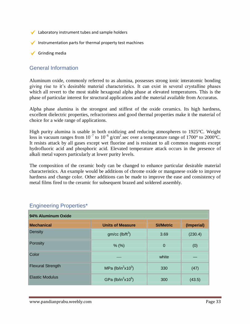
Engineering Properties*
94% Aluminum Oxide
Mechanical Units of Measure SI/Metric (Imperial)
Density gm/cc (lb/ft
3) 3.69 (230.4)
Porosity % (%) 0 (0)
Color — white —
Flexural Strength MPa (lb/in
2x10
3) 330 (47)
Elastic Modulus GPa (lb/in
2x10
6) 300 (43.5)
Page 34
www.pandianprabu.weebly.com Page 34
Shear Modulus GPa (lb/in
2x10
6) 124 (18)
Bulk Modulus GPa (lb/in
2x10
6) 165 (24)
Poisson’s Ratio — 0.21 (0.21)
Compressive Strength MPa (lb/in
2x10
3) 2100 (304.5)
Hardness Kg/mm
2 1175 —
Fracture Toughness KIC MPa•m
1/2 3.5 —
Maximum Use Temperature
(no load) °C (°F) 1700 (3090)
Thermal
Thermal Conductivity W/m•°K (BTU•in/ft
2•hr•°F) 18 (125)
Coefficient of Thermal Expansion 10
–6/°C (10
–6/°F) 8.1 (4.5)
Specific Heat J/Kg•°K (Btu/lb•°F) 880 (0.21)
Electrical
Dielectric Strength ac-kv/mm (volts/mil) 16.7 (418)
Dielectric Constant @ 1 MHz 9.1 (9.1)
Dissipation Factor @ 1 kHz 0.0007 (0.0007)
Loss Tangent @ 1 kHz — —
Volume Resistivity ohm•cm >10
14 —
96% Aluminum Oxide
Mechanical Units of Measure SI/Metric (Imperial)
Density gm/cc (lb/ft
3) 3.72 (232.2)
Porosity % (%) 0 (0)
Color — white —
Page 35
www.pandianprabu.weebly.com Page 35
Flexural Strength MPa (lb/in
2x10
3) 345 (50)
Elastic Modulus GPa (lb/in
2x10
6) 300 (43.5)
Shear Modulus GPa (lb/in
2x10
6) 124 (18)
Bulk Modulus GPa (lb/in
2x10
6) 172 (25)
Poisson’s Ratio — 0.21 (0.21)
Compressive Strength MPa (lb/in
2x10
3) 2100 (304.5)
Hardness Kg/mm
2 1100 —
Fracture Toughness KIC MPa•m
1/2 3.5 —
Maximum Use Temperature
(no load) °C (°F) 1700 (3090)
Thermal
Thermal Conductivity W/m•°K (BTU•in/ft
2•hr•°F) 25 (174)
Coefficient of Thermal Expansion 10
–6/°C (10
–6/°F) 8.2 (4.6)
Specific Heat J/Kg•°K (Btu/lb•°F) 880 (0.21)
Electrical
Dielectric Strength ac-kv/mm (volts/mil) 14.6 (365)
Dielectric Constant @ 1 MHz 9.0 (9.0)
Dissipation Factor @ 1 kHz 0.0011 (0.0011)
Loss Tangent @ 1 kHz — —
Volume Resistivity ohm•cm >10
14 —
99.5% Aluminum Oxide
Mechanical Units of Measure SI/Metric (Imperial)
Density gm/cc (lb/ft
3) 3.89 (242.8)
Page 36
www.pandianprabu.weebly.com Page 36
Porosity % (%) 0 (0)
Color — ivory —
Flexural Strength MPa (lb/in
2x10
3) 379 (55)
Elastic Modulus GPa (lb/in
2x10
6) 375 (54.4)
Shear Modulus GPa (lb/in
2x10
6) 152 (22)
Bulk Modulus GPa (lb/in
2x10
6) 228 (33)
Poisson’s Ratio — 0.22 (0.22)
Compressive Strength MPa (lb/in
2x10
3) 2600 (377)
Hardness Kg/mm
2 1440 —
Fracture Toughness KIC MPa•m
1/2 4 —
Maximum Use Temperature
(no load) °C (°F) 1750 (3180)
Thermal
Thermal Conductivity W/m°K (BTU•in/ft
2•hr•°F) 35 (243)
Coefficient of Thermal Expansion 10
–6/°C (10
–6/°F) 8.4 (4.7)
Specific Heat J/Kg•°K (Btu/lb•°F) 880 (0.21)
Electrical
Dielectric Strength ac-kv/mm (volts/mil) 16.9 (420)
Dielectric Constant @ 1 MHz 9.8 (9.8)
Dissipation Factor @ 1 kHz 0.0002 (0.0002)
Loss Tangent @ 1 kHz — —
Volume Resistivity ohm•cm >10
14 —
Page 37
www.pandianprabu.weebly.com Page 37
CUBIC BORON NITRIDE (CBN)
In 1969 General Electric launched cubic boron nitride – called
CBN for short – on to the market under the brand name
"BORAZON" as a revolutionary development in the field of
superabrasives. Produced in the retort, it achieves a Knoop intrinsic
hardness of about 4,700 N/mm2, i.e. it is more than half as hard
again as diamond (7,000 N/mm2) and not quite twice as hard as
silicon carbide (SiC) at 2,500 – 2,700 N/mm2. The originally
monocrystalline CBN, which chips rather block-like, was joined a
few years later by the microcrystalline version with completely
different, considerably finer chipping characteristics.
The spectrum of use of CBN starts at relatively soft but tough materials (from about 50 HRc) and
extends up to very hard carbide-containing alloys (tool steels, special steels, HSS, etc.). For
amorphous and ceramic materials CBN is of less suitability than for working carbides. In a
vitrified bond, the wheels can be given different profiles and/or conditioned considerably more
easily and economically.
Because of the long service life, conventional grinding wheels are now increasingly being
replaced by those of CBN, especially where production series are long or recurring. G ratios of
1,200 to 15,000 can be achieved with CBN wheels, which is 500 to about 5,000 times more than
what could be achieved with conventional grinding materials under favourable conditions of use.
CBN is used in a 1-layer electroplated form or in a resinoid, brittle bronze or vitrified bond form.
In the precision grinding sector, however, the trend is quite clearly in the direction of vitrified
bonding.
CBN grinding wheels – with the exception of wheels with an electroplated bond – are produced
in various concentrations, depending on the nature of their use. The term concentration means
the carat weight per cm3 of coat volume.
Thermal properties of CBN
CBN has a higher thermic stability than diamond. Oxidation takes place only above about
1,400ºC. The usual relatively high grinding temperatures do not attack CBN chemically during
working of either iron, nickel or cobalt. The excellent machining properties of CBN result in
"cool" grinding. The good thermal conductivity of CBN – which is about five times the heat
conductivity of copper – additionally assists this effect. When used correctly, the majority of the
grinding heat generated is therefore absorbed by the CBN grinding wheel and released to the
coolant emulsion and/or the surroundings. As a result, the workpiece heats considerably less
compared to working with corundum, since the latter can absorb far less heat.
Page 38
www.pandianprabu.weebly.com Page 38
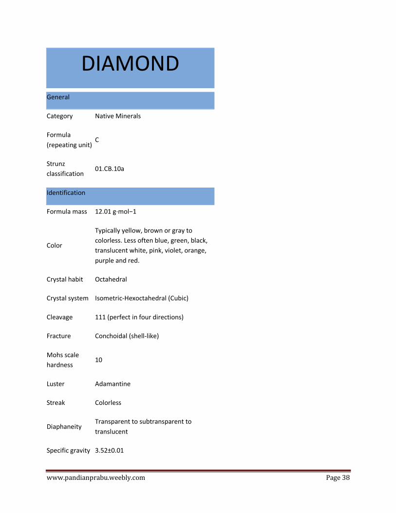
DIAMOND
General
Category Native Minerals
Formula
(repeating unit) C
Strunz
classification
01.CB.10a
Identification
Formula mass 12.01 g·mol−1
Color
Typically yellow, brown or gray to
colorless. Less often blue, green, black,
translucent white, pink, violet, orange,
purple and red.
Crystal habit Octahedral
Crystal system Isometric-Hexoctahedral (Cubic)
Cleavage 111 (perfect in four directions)
Fracture Conchoidal (shell-like)
Mohs scale
hardness 10
Luster Adamantine
Streak Colorless
Diaphaneity
Transparent to subtransparent to
translucent
Specific gravity 3.52±0.01
Page 39
www.pandianprabu.weebly.com Page 39
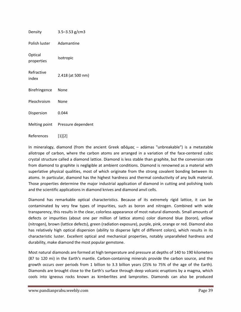
Density 3.5–3.53 g/cm3
Polish luster Adamantine
Optical
properties Isotropic
Refractive
index
2.418 (at 500 nm)
Birefringence None
Pleochroism None
Dispersion 0.044
Melting point Pressure dependent
References [1][2]
In mineralogy, diamond (from the ancient Greek αδάμας – adámas "unbreakable") is a metastable
allotrope of carbon, where the carbon atoms are arranged in a variation of the face-centered cubic
crystal structure called a diamond lattice. Diamond is less stable than graphite, but the conversion rate
from diamond to graphite is negligible at ambient conditions. Diamond is renowned as a material with
superlative physical qualities, most of which originate from the strong covalent bonding between its
atoms. In particular, diamond has the highest hardness and thermal conductivity of any bulk material.
Those properties determine the major industrial application of diamond in cutting and polishing tools
and the scientific applications in diamond knives and diamond anvil cells.
Diamond has remarkable optical characteristics. Because of its extremely rigid lattice, it can be
contaminated by very few types of impurities, such as boron and nitrogen. Combined with wide
transparency, this results in the clear, colorless appearance of most natural diamonds. Small amounts of
defects or impurities (about one per million of lattice atoms) color diamond blue (boron), yellow
(nitrogen), brown (lattice defects), green (radiation exposure), purple, pink, orange or red. Diamond also
has relatively high optical dispersion (ability to disperse light of different colors), which results in its
characteristic luster. Excellent optical and mechanical properties, notably unparalleled hardness and
durability, make diamond the most popular gemstone.
Most natural diamonds are formed at high temperature and pressure at depths of 140 to 190 kilometers
(87 to 120 mi) in the Earth's mantle. Carbon-containing minerals provide the carbon source, and the
growth occurs over periods from 1 billion to 3.3 billion years (25% to 75% of the age of the Earth).
Diamonds are brought close to the Earth′s surface through deep volcanic eruptions by a magma, which
cools into igneous rocks known as kimberlites and lamproites. Diamonds can also be produced
Page 40
www.pandianprabu.weebly.com Page 40
synthetically in a high-pressure high-temperature process which approximately simulates the conditions
in the Earth mantle. An alternative, and completely different growth technique is chemical vapor
deposition (CVD). Several non-diamond materials, which include cubic zirconia and silicon carbide and
are often called diamond simulants, resemble diamond in appearance and many properties. Special
gemological techniques have been developed to distinguish natural and synthetic diamonds and
diamond simulants.
Natural history
The formation of natural diamond requires very specific conditions—exposure of carbon-bearing
materials to high pressure, ranging approximately between 45 and 60 kilobars (4.5 and 6 GPa), but at a
comparatively low temperature range between approximately 900–1300 °C (1652–2372 °F). These
conditions are met in two places on Earth; in the lithospheric mantle below relatively stable continental
plates, and at the site of a meteorite strike.[10]
Formation in cratons
One face of an uncut octahedral diamond, showing trigons (of positive and negative relief) formed by
natural chemical etching
The conditions for diamond formation to happen in the lithospheric mantle occur at considerable depth
corresponding to the requirements of temperature and pressure. These depths are estimated between
140 and 190 kilometers (87 and 120 mi) though occasionally diamonds have crystallized at depths about
300 kilometers (190 mi).[11] The rate at which temperature changes with increasing depth into the
Earth varies greatly in different parts of the Earth. In particular, under oceanic plates the temperature
rises more quickly with depth, beyond the range required for diamond formation at the depth required.
The correct combination of temperature and pressure is only found in the thick, ancient, and stable
parts of continental plates where regions of lithosphere known as cratons exist. Long residence in the
cratonic lithosphere allows diamond crystals to grow larger.[11]
Through studies of carbon isotope ratios (similar to the methodology used in carbon dating, except with
the stable isotopes C-12 and C-13), it has been shown that the carbon found in diamonds comes from
both inorganic and organic sources. Some diamonds, known as harzburgitic, are formed from inorganic
Page 41
www.pandianprabu.weebly.com Page 41
carbon originally found deep in the Earth's mantle. In contrast, eclogitic diamonds contain organic
carbon from organic detritus that has been pushed down from the surface of the Earth's crust through
subduction (see plate tectonics) before transforming into diamond. These two different source of
carbon have measurably different 13C:12C ratios. Diamonds that have come to the Earth's surface are
generally quite old, ranging from under 1 billion to 3.3 billion years old. This is 22% to 73% of the age of
the Earth.[11]
Diamonds occur most often as euhedral or rounded octahedra and twinned octahedra known as macles.
As diamond's crystal structure has a cubic arrangement of the atoms, they have many facets that belong
to a cube, octahedron, rhombicosidodecahedron, tetrakis hexahedron or disdyakis dodecahedron. The
crystals can have rounded off and unexpressive edges and can be elongated. Sometimes they are found
grown together or form double "twinned" crystals at the surfaces of the octahedron. These different
shapes and habits of some diamonds result from differing external circumstances. Diamonds (especially
those with rounded crystal faces) are commonly found coated in nyf, an opaque gum-like skin.
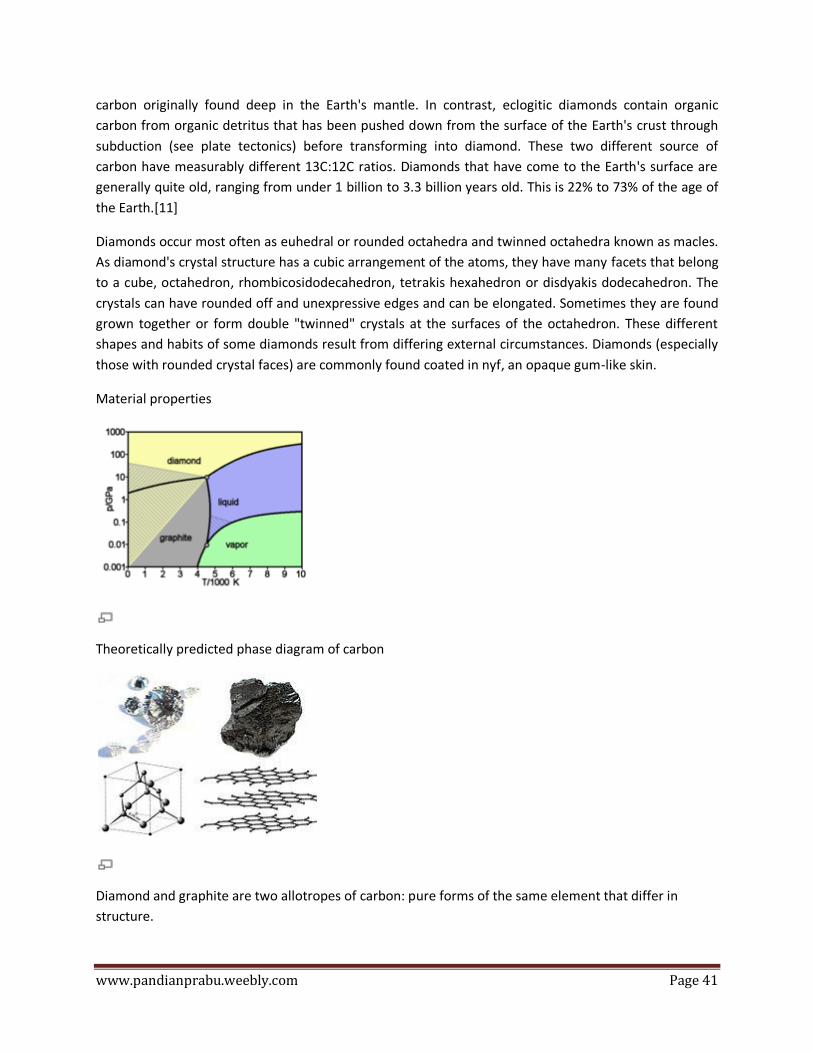
Material properties
Theoretically predicted phase diagram of carbon
Diamond and graphite are two allotropes of carbon: pure forms of the same element that differ in
structure.
Page 42
www.pandianprabu.weebly.com Page 42
A diamond is a transparent crystal of tetrahedrally bonded carbon atoms in a covalent network lattice
(sp3) that crystallizes into the diamond lattice which is a variation of the face centered cubic structure.
Diamonds have been adapted for many uses because of the material's exceptional physical
characteristics. Most notable are its extreme hardness and thermal conductivity (900–2,320
W·m−1·K−1),[20] as well as wide bandgap and high optical dispersion.[21] Above 1,700 °C (1,973 K /
3,583 °F) in vacuum or oxygen-free atmosphere, diamond converts to graphite; in air, transformation
starts at ~700 °C.[22] Diamond's ignition point is 720 - 800 °C in oxygen and 850 - 1,000 °C in air.[23]
Naturally occurring diamonds have a density ranging from 3.15–3.53 g/cm3, with pure diamond close to
3.52 g/cm3.[1] The chemical bonds that hold the carbon atoms in diamonds together are weaker than
those in graphite. In diamonds, the bonds form an inflexible three-dimensional lattice, whereas in
graphite, the atoms are tightly bonded into sheets, which can slide easily over one another, making the
overall structure weaker.
Hardness
Diamond is the hardest known natural material on the Mohs scale of mineral hardness, where hardness
is defined as resistance to scratching and is graded between 1 (softest) and 10 (hardest). Diamond has a
hardness of 10 (hardest) on this scale.[25] Diamond's hardness has been known since antiquity, and is
the source of its name.
Diamond hardness depends on its purity, crystalline perfection and orientation: hardness is higher for
flawless, pure crystals oriented to the <111> direction (along the longest diagonal of the cubic diamond
lattice).[26] Therefore, whereas it might be possible to scratch some diamonds with other materials,
such as boron nitride, the hardest diamonds can only be scratched by other diamonds and
nanocrystalline diamond aggregates.
The hardness of diamond contributes to its suitability as a gemstone. Because it can only be scratched
by other diamonds, it maintains its polish extremely well. Unlike many other gems, it is well-suited to
daily wear because of its resistance to scratching—perhaps contributing to its popularity as the
preferred gem in engagement or wedding rings, which are often worn every day.
The extreme hardness of diamond in certain orientations makes it useful in materials science, as in this
pyramidal diamond embedded in the working surface of a Vickers hardness tester.
Page 43
www.pandianprabu.weebly.com Page 43
The hardest natural diamonds mostly originate from the Copeton and Bingara fields located in the New
England area in New South Wales, Australia. These diamonds are generally small, perfect to semiperfect
octahedra, and are used to polish other diamonds. Their hardness is associated with the crystal growth
form, which is single-stage crystal growth. Most other diamonds show more evidence of multiple growth
stages, which produce inclusions, flaws, and defect planes in the crystal lattice, all of which affect their
hardness. It is possible to treat regular diamonds under a combination of high pressure and high
temperature to produce diamonds that are harder than the diamonds used in hardness gauges.
Somewhat related to hardness is another mechanical property toughness, which is a material's ability to
resist breakage from forceful impact. The toughness of natural diamond has been measured as 7.5–10
MPa·m1/2.[27][28] This value is good compared to other gemstones, but poor compared to most
engineering materials. As with any material, the macroscopic geometry of a diamond contributes to its
resistance to breakage. Diamond has a cleavage plane and is therefore more fragile in some orientations
than others. Diamond cutters use this attribute to cleave some stones, prior to faceting.[29] "Impact
toughness" is one of the main indexes to measure the quality of synthetic industrial diamonds.
Electrical conductivity
Other specialized applications also exist or are being developed, including use as semiconductors: some
blue diamonds are natural semiconductors, in contrast to most diamonds, which are excellent electrical
insulators.[30] The conductivity and blue color originate from boron impurity. Boron substitutes for
carbon atoms in the diamond lattice, donating a hole into the valence band.
Substantial conductivity is commonly observed in nominally undoped diamond grown by chemical vapor
deposition. This conductivity is associated with hydrogen-related species adsorbed at the surface, and it
can be removed by annealing or other surface treatments.
Surface property
Diamonds are lipophilic and hydrophobic, which means the diamonds' surface cannot be wet by water
but can be easily wet and stuck by oil. This property can be utilized to extract diamonds using oil when
making synthetic diamonds.
Chemical stability
Diamonds are not very reactive. Under room temperature diamonds do not react with any chemical
reagents including strong acids and bases. A diamond's surface can only be oxidized a little by just a few
oxidants[which?] at high temperature (below 1,000 °C). Therefore, acids and bases can be used to refine
synthetic diamonds.
Color
Page 44
www.pandianprabu.weebly.com Page 44
Brown diamonds at the National Museum of Natural History in Washington, D.C.
Diamond has a wide bandgap of 5.5 eV corresponding to the deep ultraviolet wavelength of 225
nanometers. This means pure diamond should transmit visible light and appear as a clear colorless
crystal. Colors in diamond originate from lattice defects and impurities. The diamond crystal lattice is
exceptionally strong and only atoms of nitrogen, boron and hydrogen can be introduced into diamond
during the growth at significant concentrations (up to atomic percents). Transition metals Ni and Co,
which are commonly used for growth of synthetic diamond by high-pressure high-temperature
techniques, have been detected in diamond as individual atoms; the maximum concentration is 0.01%
for Ni[33] and even much less for Co. Virtually any element can be introduced to diamond by ion
implantation.
Nitrogen is by far the most common impurity found in gem diamonds and is responsible for the yellow
and brown color in diamonds. Boron is responsible for the blue color.[21] Color in diamond has two
additional sources: irradiation (usually by alpha particles), that causes the color in green diamonds; and
plastic deformation of the diamond crystal lattice. Plastic deformation is the cause of color in some
brown[35] and perhaps pink and red diamonds.[36] In order of rarity, yellow diamond is followed by
brown, colorless, then by blue, green, black, pink, orange, purple, and red.[29] "Black", or Carbonado,
diamonds are not truly black, but rather contain numerous dark inclusions that give the gems their dark
appearance. Colored diamonds contain impurities or structural defects that cause the coloration, while
pure or nearly pure diamonds are transparent and colorless. Most diamond impurities replace a carbon
atom in the crystal lattice, known as a carbon flaw. The most common impurity, nitrogen, causes a slight
to intense yellow coloration depending upon the type and concentration of nitrogen present.[29] The
Gemological Institute of America (GIA) classifies low saturation yellow and brown diamonds as
diamonds in the normal color range, and applies a grading scale from "D" (colorless) to "Z" (light yellow).
Diamonds of a different color, such as blue, are called fancy colored diamonds, and fall under a different
grading scale.
In 2008, the Wittelsbach Diamond, a 35.56-carat (7.11 g) blue diamond once belonging to the King of
Spain, fetched over US$24 million at a Christie's auction.[37] In May 2009, a 7.03-carat (1.41 g) blue
diamond fetched the highest price per carat ever paid for a diamond when it was sold at auction for 10.5
million Swiss francs (6.97 million euro or US$9.5 million at the time).[38] That record was however
Page 45
www.pandianprabu.weebly.com Page 45
beaten the same year: a 5-carat (1.0 g) vivid pink diamond was sold for $10.8 million in Hong Kong on
December 1, 2009.
Identification
Diamonds can be identified by their high thermal conductivity. Their high refractive index is also
indicative, but other materials have similar refractivity. Diamonds cut glass, but this does not positively
identify a diamond because other materials, such as quartz, also lie above glass on the Mohs scale and
can also cut it. Diamonds can scratch other diamonds, but this can result in damage to one or both
stones. Hardness tests are infrequently used in practical gemology because of their potentially
destructive nature.[25] The extreme hardness and high value of diamond means that gems are typically
polished slowly using painstaking traditional techniques and greater attention to detail than is the case
with most other gemstones;[8] these tend to result in extremely flat, highly polished facets with
exceptionally sharp facet edges. Diamonds also possess an extremely high refractive index and fairly
high dispersion. Taken together, these factors affect the overall appearance of a polished diamond and
most diamantaires still rely upon skilled use of a loupe (magnifying glass) to identify diamonds 'by eye'.
Industry
A round brilliant cut diamond set in a ring
Cutting
Page 46
www.pandianprabu.weebly.com Page 46
The Darya-I-Nur Diamond—an example of unusual diamond cut and jewelry arrangement
Mined rough diamonds are converted into gems through a multi-step process called "cutting".
Diamonds are extremely hard, but also brittle and can be split up by a single blow. Therefore, diamond
cutting is traditionally considered as a delicate procedure requiring skills, scientific knowledge, tools and
experience. Its final goal is to produce a faceted jewel where the specific angles between the facets
would optimize the diamond luster, that is dispersion of white light, whereas the number and area of
facets would determine the weight of the final product. The weight reduction upon cutting is significant
and can be of the order of 50%.[61] Several possible shapes are considered, but the final decision is
often determined not only by scientific, but also practical considerations. For example the diamond
might be intended for display or for wear, in a ring or a necklace, singled or surrounded by other gems
of certain color and shape.
The most time-consuming part of the cutting is the preliminary analysis of the rough stone. It needs to
address a large number of issues, bears much responsibility, and therefore can last years in case of
unique diamonds. The following issues are considered:
The hardness of diamond and its ability to cleave strongly depend on the crystal orientation. Therefore,
the crystallographic structure of the diamond to be cut is analyzed using X-ray diffraction to choose the
optimal cutting directions.
Most diamonds contain visible non-diamond inclusions and crystal flaws. The cutter has to decide which
flaws are to be removed by the cutting and which could be kept.
The diamond can be split by a single, well calculated blow of a hammer to a pointed tool, which is quick,
but risky. Alternatively, it can be cut with a diamond saw, which is a more reliable but tedious
procedure.
After initial cutting, the diamond is shaped in numerous stages of polishing. Unlike cutting, which is a
responsible but quick operation, polishing removes material by gradual erosion and is extremely time
consuming. The associated technique is well developed; it is considered as a routine and can be
performed by technicians.[64] After polishing, the diamond is reexamined for possible flaws, either
remaining or induced by the process. Those flaws are concealed through various diamond enhancement
techniques, such as repolishing, crack filling, or clever arrangement of the stone in the jewelry.
Remaining non-diamond inclusions are removed through laser drilling and filling of the voids produced.
If buyers are only able to purchase the diamond mounted, so that buyers are unable to fully inspect the
product, or if the diamond comes without a full GIA lab grading report, or a written guarantee that it
was sourced from a legitimate supplier, these are other indicators of a lower valued diamond.[72]
Industrial-grade diamonds
Page 47
www.pandianprabu.weebly.com Page 47
A scalpel with synthetic diamond blade
Close-up photograph of an angle grinder blade with tiny diamonds shown embedded in the metal
Industrial diamonds are valued mostly for their hardness and thermal conductivity, making many of the
gemological characteristics of diamonds, such as the 4 Cs, irrelevant for most applications. This helps
explain why 80% of mined diamonds (equal to about 135,000,000 carats (27,000 kg) annually),
unsuitable for use as gemstones, are destined for industrial use. In addition to mined diamonds,
synthetic diamonds found industrial applications almost immediately after their invention in the 1950s;
another 570,000,000 carats (110,000 kg) of synthetic diamond is produced annually for industrial use.
Approximately 90% of diamond grinding grit is currently of synthetic origin.
The boundary between gem-quality diamonds and industrial diamonds is poorly defined and partly
depends on market conditions (for example, if demand for polished diamonds is high, some suitable
stones will be polished into low-quality or small gemstones rather than being sold for industrial use).
Within the category of industrial diamonds, there is a sub-category comprising the lowest-quality,
mostly opaque stones, which are known as bort.
Page 48
www.pandianprabu.weebly.com Page 48
Industrial use of diamonds has historically been associated with their hardness; this property makes
diamond the ideal material for cutting and grinding tools. As the hardest known naturally occurring
material, diamond can be used to polish, cut, or wear away any material, including other diamonds.
Common industrial adaptations of this ability include diamond-tipped drill bits and saws, and the use of
diamond powder as an abrasive. Less expensive industrial-grade diamonds, known as bort, with more
flaws and poorer color than gems, are used for such purposes.[75] Diamond is not suitable for
machining ferrous alloys at high speeds, as carbon is soluble in iron at the high temperatures created by
high-speed machining, leading to greatly increased wear on diamond tools compared to alternatives.
Specialized applications include use in laboratories as containment for high pressure experiments (see
diamond anvil cell), high-performance bearings, and limited use in specialized windows.[74] With the
continuing advances being made in the production of synthetic diamonds, future applications are
becoming feasible. Garnering much excitement is the possible use of diamond as a semiconductor
suitable to build microchips, or the use of diamond as a heat sink[77] in electronics.
Mining
Approximately 130,000,000 carats (26,000 kg) of diamonds are mined annually, with a total value of
nearly US$9 billion, and about 100,000 kg (220,000 lb) are synthesized annually.
Roughly 49% of diamonds originate from Central and Southern Africa, although significant sources of the
mineral have been discovered in Canada, India, Russia, Brazil, and Australia.[73] They are mined from
kimberlite and lamproite volcanic pipes, which can bring diamond crystals, originating from deep within
the Earth where high pressures and temperatures enable them to form, to the surface. The mining and
distribution of natural diamonds are subjects of frequent controversy such as concerns over the sale of
blood diamonds or conflict diamonds by African paramilitary groups.[79] The diamond supply chain is
controlled by a limited number of powerful businesses, and is also highly concentrated in a small
number of locations around the world.
Only a very small fraction of the diamond ore consists of actual diamonds. The ore is crushed, during
which care is required not to destroy larger diamonds, and then sorted by density. Today, diamonds are
located in the diamond-rich density fraction with the help of X-ray fluorescence, after which the final
sorting steps are done by hand. Before the use of X-rays became commonplace,[61] the separation was
done with grease belts; diamonds have a stronger tendency to stick to grease than the other minerals in
the ore.
Page 49
www.pandianprabu.weebly.com Page 49
Siberia's Udachnaya diamond mine
Historically, diamonds were found only in alluvial deposits in Guntur and Krishna district of the Krishna
River delta in Southern India.[80] India led the world in diamond production from the time of their
discovery in approximately the 9th century BC[4][81] to the mid-18th century AD, but the commercial
potential of these sources had been exhausted by the late 18th century and at that time India was
eclipsed by Brazil where the first non-Indian diamonds were found in 1725.[4] Currently, one of the
most prominent Indian mines is located at Panna.[82]
Diamond extraction from primary deposits (kimberlites and lamproites) started in the 1870s after the
discovery of the Diamond Fields in South Africa.[83] Production has increased over time and now an
accumulated total of 4,500,000,000 carats (900,000 kg) have been mined since that date.[84] Twenty
percent of that amount has been mined in the last five years, and during the last 10 years, nine new
mines have started production; four more are waiting to be opened soon. Most of these mines are
located in Canada, Zimbabwe, Angola, and one in Russia.[84]
In the U.S., diamonds have been found in Arkansas, Colorado, Wyoming, and Montana.[85][86] In 2004,
the discovery of a microscopic diamond in the U.S. led to the January 2008 bulk-sampling of kimberlite
pipes in a remote part of Montana.
Today, most commercially viable diamond deposits are in Russia (mostly in Sakha Republic, for example
Mir pipe and Udachnaya pipe), Botswana, Australia (Northern and Western Australia) and the
Democratic Republic of Congo.[87] In 2005, Russia produced almost one-fifth of the global diamond
output, reports the British Geological Survey. Australia boasts the richest diamantiferous pipe, with
production from the Argyle diamond mine reaching peak levels of 42 metric tons per year in the
1990s.[85][88] There are also commercial deposits being actively mined in the Northwest Territories of
Canada and Brazil.[73] Diamond prospectors continue to search the globe for diamond-bearing
kimberlite and lamproite pipes.
Synthetics
Synthetic diamonds of various colors grown by the high-pressure high-temperature technique
Page 50
www.pandianprabu.weebly.com Page 50
Synthetic diamonds are diamonds manufactured in a laboratory, as opposed to diamonds mined from
the Earth. The gemological and industrial uses of diamond have created a large demand for rough
stones. This demand has been satisfied in large part by synthetic diamonds, which have been
manufactured by various processes for more than half a century. However, in recent years it has
become possible to produce gem-quality synthetic diamonds of significant size.[11]
The majority of commercially available synthetic diamonds are yellow and are produced by so-called
High Pressure High Temperature (HPHT) processes.[93] The yellow color is caused by nitrogen
impurities. Other colors may also be reproduced such as blue, green or pink, which are a result of the
addition of boron or from irradiation after synthesis.[94]
Colorless gem cut from diamond grown by chemical vapor deposition
Another popular method of growing synthetic diamond is chemical vapor deposition (CVD). The growth
occurs under low pressure (below atmospheric pressure). It involves feeding a mixture of gases (typically
1 to 99 methane to hydrogen) into a chamber and splitting them to chemically active radicals in a
plasma ignited by microwaves, hot filament, arc discharge, welding torch or laser.[95] This method is
mostly used for coatings, but can also produce single crystals several millimeters in size (see
picture).[78]
At present, the annual production of gem quality synthetic diamonds is only a few thousand carats,
whereas the total production of natural diamonds is around 120,000,000 carats (24,000 kg). Despite this
fact, a purchaser is more likely to encounter a synthetic when looking for a fancy-colored diamond
because nearly all synthetic diamonds are fancy-colored, while only 0.01% of natural diamonds are.[96]
Simulants
Page 51
www.pandianprabu.weebly.com Page 51
Gem-cut synthetic silicon carbide set in a ring
A diamond simulant is a non-diamond material that is used to simulate the appearance of a diamond,
and may be referred to as diamante. Cubic zirconia is the most common. The gemstone Moissanite
(silicon carbide) can be treated as a diamond simulant, though more costly to produce than cubic
zirconia. Both are produced synthetically
Enhancements
Diamond enhancements are specific treatments performed on natural or synthetic diamonds (usually
those already cut and polished into a gem), which are designed to better the gemological characteristics
of the stone in one or more ways. These include laser drilling to remove inclusions, application of
sealants to fill cracks, treatments to improve a white diamond's color grade, and treatments to give
fancy color to a white diamond.[98]
Coatings are increasingly used to give a diamond simulant such as cubic zirconia a more "diamond-like"
appearance. One such substance is diamond-like carbon—an amorphous carbonaceous material that
has some physical properties similar to those of the diamond. Advertising suggests that such a coating
would transfer some of these diamond-like properties to the coated stone, hence enhancing the
diamond simulant. Techniques such as Raman spectroscopy should easily identify such a treatment.[99]
Identification
Early diamond identification tests included a scratch test relying on the superior hardness of diamond.
This test is destructive, as a diamond can scratch diamond, and is rarely used nowadays. Instead,
diamond identification relies on its superior thermal conductivity. Electronic thermal probes are widely
used in the gemological centers to separate diamonds from their imitations. These probes consist of a
pair of battery-powered thermistors mounted in a fine copper tip. One thermistor functions as a heating
device while the other measures the temperature of the copper tip: if the stone being tested is a
diamond, it will conduct the tip's thermal energy rapidly enough to produce a measurable temperature
drop. This test takes about 2–3 seconds.[100]
Whereas the thermal probe can separate diamonds from most of their simulants, distinguishing
between various types of diamond, for example synthetic or natural, irradiated or non-irradiated, etc.,
requires more advanced, optical techniques. Those techniques are also used for some diamonds
simulants, such as silicon carbide, which pass the thermal conductivity test. Optical techniques can
distinguish between natural diamonds and synthetic diamonds. They can also identify the vast majority
of treated natural diamonds.[101] "Perfect" crystals (at the atomic lattice level) have never been found,
so both natural and synthetic diamonds always possess characteristic imperfections, arising from the
circumstances of their crystal growth, that allow them to be distinguished from each other.[102]
Page 52
www.pandianprabu.weebly.com Page 52
Laboratories use techniques such as spectroscopy, microscopy and luminescence under shortwave
ultraviolet light to determine a diamond's origin.[101] They also use specially made instruments to aid
them in the identification process. Two screening instruments are the DiamondSure and the
DiamondView, both produced by the DTC and marketed by the GIA.[103]
Several methods for identifying synthetic diamonds can be performed, depending on the method of
production and the color of the diamond. CVD diamonds can usually be identified by an orange
fluorescence. D-J colored diamonds can be screened through the Swiss Gemmological Institute's[104]
Diamond Spotter. Stones in the D-Z color range can be examined through the DiamondSure UV/visible
spectrometer, a tool developed by De Beers.[102] Similarly, natural diamonds usually have minor
imperfections and flaws, such as inclusions of foreign material, that are not seen in synthetic diamonds.
Diamond cutting
Diamond cutting is the practice of changing a diamond from a rough stone into a faceted gem.
Cutting diamond requires specialized knowledge, tools, equipment, and techniques because of its
extreme difficulty.
The first guild of diamond cutters and polishers (diamantaire) was formed in 1375 in Nuremberg,
Germany, and led to the development of various types of 'cut'. This has two meanings in relation
to diamonds. The first is the shape: square, oval, and so on. The second relates to the specific
quality of cut within the shape, and the quality and price will vary greatly based on the cut
quality. Since diamonds are very hard to cut, special diamond-bladed edges are used to cut them.
The first major development in diamond cutting came with the "Point Cut" during the later half
of the 14th century: the Point Cut follows the natural shape of an octahedral raw diamond
crystal, eliminating some waste in the cutting process.
Cutting process
It is possible only because the hardness of diamond varies widely according to the direction in
which one is trying to cut or grind.
A simplified round brilliant cut process includes the following stages:
Sawing the rough stone. Table setting where one facet is created. The table facet is then used to attach the stone into a
dop (a lapidary tool holding gemstones for cutting or polishing). Bruting the girdle. Blocking four main pavilion facets. Transferring to another dop in order to rotate the stone. Blocking four main crown facets. Cutting and polishing all pavilion facets.
Page 53
www.pandianprabu.weebly.com Page 53
Transferring to another dop. Cutting and polishing all crown facets.
This is just one, although a fairly common way of creating a round brilliant cut. The actual
process also includes many more stages depending on the size and quality of the rough stone. For
example, bigger stones are first scanned to get the three-dimensional shape, which is then used to
find the optimal usage. The scanning may be repeated after each stage and bruting may be done
in several steps, each bringing the girdle closer to the final shape.
Silicon Carbide (SiC)– Synthesis, Properties
and Applications {TOPIC 1}
Topics Covered
What is Silicon Carbide?
Synthesizing Silicon Carbide
The Structure of Silicon Carbide
The Discovery of Silicon Carbide
Types of Silicon Carbide
Key Properties of Silicon Carbide
Major Applications of Silicon Carbide
Machining of Silicon Carbide
Insaco
What is Silicon Carbide?
The Chemical Formula of Silicon Carbide, which is also known carborundum, is SiC. It is
produced by the carbothermal reduction of silica to form an ultra-hard covalently bonded
material. It is extremely rare in nature but can be found in the mineral moissanite, which was
first discovered in Arizona in 1893.
Page 54
www.pandianprabu.weebly.com Page 54
Precision machined sintered silicon carbide component produced by Insaco.
Synthesizing Silicon Carbide
Typically, Silicon Carbide is produced using the Acheson process which involves heating silica
sand and carbon to high temperatures in an Acheson graphite resistance furnace. It can be formed
as a fine powder or a bonded mass that must be crushed and milled before it can be used as a
powder feedstock. Once the Silicon Carbide is in a powder form, the grains of the compound can
be bonded together by sintering to form a very useful engineering ceramic, which has a wide
range of uses in many manufacturing industries.
The Structure of Silicon Carbide
Many structures or polytypes have been identified for Silicon Carbide. These polytypes have
different stacking arrangements for the atoms of silicon and carbon in the compound. One of the
simplest structures is the diamond structure, which is known as b -SiC. There are more complex
hexagonal or rhombic structures of the compound and these are designated as a -SiC.
The Discovery of Silicon Carbide
Dr. Edward Goodrich Acheson was a scientist who once worked for Thomas Edison. He first
synthesized Silicon Carbide by chance in the process of trying to create artificial diamonds.
Diamonds could be, at least in theory, baked in the laboratory and so he decided to attempt to
synthesize them using carbon based materials. In his experiment he attached a lead from a
dynamo to a plumber‘s bowl, which was filled with clay and powdered coke.
When the mixture was subjected to the high heating temperature from the dynamo lead, he did
not produce any diamonds, but he did notice a few bright specks on the end of the lead. He
picked up the lead and drew it over a glass pane and it cut the pane like a diamond. What he had
succeeded in developing was, the first man made substance that was hard enough to cut through
glass.
He was also trying to dissolve carbon in molten corundum or alumina when he discovered the
blue black colored crystals which he thought were a compound of corundum and carbon, hence
why he called the material carborundum. This became the popular name for Silicon Carbide and
was also the name of the company that Acheson founded. Although the first use of the
compound was as an abrasive, it has since been subsequently developed to be used in electronic
applications and many other engineering uses.
Types of Silicon Carbide
For use in commercial engineering applications Silicon Carbide products are produced in three
forms. These are:
Sintered silicon carbide (SSC)
Page 55
www.pandianprabu.weebly.com Page 55
Nitride bonded silicon carbide (NBSC) and Reaction bonded silicon carbide (RBSC)
Other variations of the compound include clay bonded silicon carbide and SiAlON bonded
silicon carbide. There is also chemical vapor deposited silicon carbide called CVD Silicon
Carbide, which is an extremely pure form of the compound.
To sinter the Silicon Carbide its is necessary to add sintering aids which help to form a liquid
phase at the sintering temperature which allows the grains of silicon carbide to bond together.
Key Properties of Silicon Carbide
Silicon Carbide has a refractive index that is greater than that of diamond. It has a high thermal
conductivity and it has a low thermal expansion coefficient. This combination of these properties
give it outstanding thermal shock resistance, which makes it useful to many industries. It is also a
semiconductor and lends itself to a range of uses thanks to its electrical properties. It is also
known for its extreme hardness and is very corrosion resistant.
The Table below provides further example data for Sintered Silicon Carbide.
Table 1. Properties of sintered silicon carbide.
Property Minimum
Value (S.I.)
Maximum
Value (S.I.)
Units
(S.I.)
Minimum
Value (Imp.)
Maximum
Value (Imp.) Units (Imp.)
Atomic Volume
(average) 0.0062 0.0064 m3/kmol 378.347 390.552 in3/kmol
Density 3 3.2 Mg/m3 187.284 199.77 lb/ft3
Energy Content 150 200 MJ/kg 16250.8 21667.7 kcal/lb
Bulk Modulus 181 189.8 GPa 26.2518 27.5281 106 psi
Compressive
Strength 3047.4 3359.9 MPa 441.988 487.312 ksi
Ductility 0.00076 0.00084
0.00076 0.00084 NULL
Elastic Limit 304.7 336 MPa 44.193 48.7327 ksi
Endurance Limit 259.17 302.37 MPa 37.5894 43.855 ksi
Fracture Toughness 4.28 4.72 MPa.m1/2 3.895 4.29542 ksi.in1/2
Hardness 23800 26250 MPa 3451.9 3807.24 ksi
Page 56
www.pandianprabu.weebly.com Page 56
Loss Coefficient 2e-005 5e-005
2e-005 5e-005 NULL
Modulus of Rupture 365.7 403.2 MPa 53.0403 58.4792 ksi
Poisson's Ratio 0.13 0.15
0.13 0.15 NULL
Shear Modulus 171.15 179.8 GPa 24.8232 26.0778 106 psi
Tensile Strength 304.7 336 MPa 44.193 48.7327 ksi
Young's Modulus 390.2 410 GPa 56.5937 59.4654 106 psi
Latent Heat of
Fusion 930 1050 kJ/kg 399.826 451.416 BTU/lb
Maximum Service
Temperature 1738 1808 K 2668.73 2794.73 °F
Melting Point 2424 2522 K 3903.53 4079.93 °F
Minimum Service
Temperature 0 0 K -459.67 -459.67 °F
Specific Heat 663 677 J/kg.K 0.513068 0.523902 BTU/lb.F
Thermal
Conductivity 90 110 W/m.K 168.483 205.924 BTU.ft/h.ft2.F
Thermal Expansion 2.7 2.8 10-6/K 4.86 5.04 10-6/°F
Breakdown
Potential 5 10 MV/m 127 254 V/mil
Dielectric Constant 7 9
7 9 NULL
Resistivity 1e+009 3.16e+010 10-8
ohm.m 1e+009 3.16e+010 10-8 ohm.m
Major Applications of Silicon Carbide
There are many uses of Silicon Carbide in different industries. Its physical hardness makes it
ideal to be used in abrasive machining processes like grinding, honing, sand blasting and water
jet cutting.
The ability of Silicon Carbide to withstand very high temperatures without breaking or distorting
is used in the manufacture of ceramic brake discs for sports cars. It is also used in bulletproof
vests as an armor material and as a seal ring material for pump shaft sealing where it frequently
Page 57
www.pandianprabu.weebly.com Page 57
runs at high speed in contact with a similar silicon carbide seal. One of the major advantages in
these applications being the high thermal conductivity of Silicon Carbide which is able to
dissipate the frictional heat generated at a rubbing interface.
The high surface hardness of the material lead to it being used in many engineering applications
where a high degree of sliding, erosive and corrosive wear resistance is required. Typically this
can be in components used in pumps or for example as valves in oilfield applications where
conventional metal components would display excessive wear rates that would lead to rapid
failures.
The unique electrical properties of the compound as a semiconductor make it ideal for
manufacturing ultra fast and high voltage light emitting diodes, MOSFETs and thyristors for
high power switching.
The material‘s low thermal expansion coefficient, hardness, rigidity and thermal conductivity
make it an ideal mirror material for astronomical telescopes. Silicon Carbide fibers, known as
filaments are used to measure gas temperatures in an optical technique called thin filament
pyrometry.
It is also used in heating elements where extremely high temperatures need to be accommodated.
It is even used in nuclear power to provide structural supports in high temperature gas cooled
reactors.
Machining of Silicon Carbide
In all of the applications outlined above, where a high precision engineering components are
required, it is important to recognize the difficulties of machining Silicon Carbide. Despite the
high hardness values it displays, it is nevertheless a relatively brittle material and can only be
machined using diamond grinding techniques. Consequently, it is beneficial that a skilled and
experienced operator conducts the machining operations as incorrect procedures can generate
sub-surface damage and micro-cracks that may lead to premature failure once the component is
subjected to operating stresses in service.
Silicon Carbide, SiC Material Properties {TOPIC 2}
Silicon Carbide is the only chemical compound of carbon and silicon. It was originally produced
by a high temperature electro-chemical reaction of sand and carbon. Silicon carbide is an
excellent abrasive and has been produced and made into grinding wheels and other abrasive
products for over one hundred years. Today the material has been developed into a high quality
technical grade ceramic with very good mechanical properties. It is used in abrasives,
refractories, ceramics, and numerous high-performance applications. The material can also be
made an electrical conductor and has applications in resistance heating, flame igniters and
electronic components. Structural and wear applications are constantly developing.
Page 58
www.pandianprabu.weebly.com Page 58
.Key Silicon Carbide Properties
Low density
High strength
Low thermal expansion
High thermal conductivity
High hardness
High elastic modulus
Excellent thermal shock resistance
Superior chemical inertness
.
Silicon Carbide Typical Uses
Fixed and moving turbine components
Suction box covers
Seals, bearings
Ball valve parts
Hot gas flow liners
Heat exchangers
Semiconductor process equipment
General Silicon Carbide Information
Silicon carbide is composed of tetrahedra of carbon and silicon atoms with strong bonds in the
crystal lattice. This produces a very hard and strong material. Silicon carbide is not attacked by
any acids or alkalis or molten salts up to 800°C. In air, SiC forms a protective silicon oxide
coating at 1200°C and is able to be used up to 1600°C. The high thermal conductivity coupled
with low thermal expansion and high strength give this material exceptional thermal shock
resistant qualities. Silicon carbide ceramics with little or no grain boundary impurities maintain
their strength to very high temperatures, approaching 1600°C with no strength loss. Chemical
purity, resistance to chemical attack at temperature, and strength retention at high temperatures
has made this material very popular as wafer tray supports and paddles in semiconductor
furnaces. The electrical conduction of the material has lead to its use in resistance heating
Page 59
www.pandianprabu.weebly.com Page 59
elements for electric furnaces, and as a key component in thermistors (temperature variable
resistors) and in varistors (voltage variable resistors).
Silicon Carbide Engineering Properties*
Silicon Carbide Properties
Mechanical SI/Metric (Imperial) SI/Metric (Imperial)
Density gm/cc (lb/ft
3) 3.1 (193.5)
Porosity % (%) 0 (0)
Color — black —
Flexural Strength MPa (lb/in
2x10
3) 550 (80)
Elastic Modulus GPa (lb/in
2x10
6) 410 (59.5)
Shear Modulus GPa (lb/in
2x10
6) — —
Bulk Modulus GPa (lb/in
2x10
6) — —
Poisson’s Ratio — 0.14 (0.14)
Compressive Strength MPa (lb/in
2x10
3) 3900 (566)
Hardness Kg/mm
2 2800 —
Fracture Toughness KIC MPa•m
1/2 4.6 —
Maximum Use Temperature
(no load) °C (°F) 1650 (3000)
Thermal
Thermal Conductivity W/m•°K (BTU•in/ft
2•hr•°F) 120 (830)
Coefficient of Thermal Expansion 10
–6/°C (10
–6/°F) 4.0 (2.2)
Specific Heat J/Kg•°K (Btu/lb•°F) 750 (0.18)
Electrical
Dielectric Strength ac-kv/mm (volts/mil) — semiconductor
Dielectric Constant — — —
Page 60
www.pandianprabu.weebly.com Page 60
Dissipation Factor — — —
Loss Tangent — — —
Volume Resistivity ohm•cm 10
2–10
6 dopant dependent
Sic {TOPIC 3}
Properties
Molecular formula CSi
Molar mass 40.1 g mol−1
Appearance Colorless crystals
Density 3.21 g·cm−3 (all polytypes)[1]
Melting point
2730 °C, 3003 K, 4946 °F
(decomposes)
Electron mobility ~900 cm2/V·s (all polytypes)
Refractive index
(nD) 2.55 (infrared; all polytypes)[2]
Page 61
www.pandianprabu.weebly.com Page 61
Hazards
EU classification Not listed
NFPA 704
0
1
0
Silicon carbide (SiC), also known as carborundum /kɑrbəˈrʌndəm/, is a compound of silicon and carbon
with chemical formula SiC. It occurs in nature as the extremely rare mineral moissanite. Silicon carbide
powder has been mass-produced since 1893 for use as an abrasive. Grains of silicon carbide can be
bonded together by sintering to form very hard ceramics which are widely used in applications requiring
high endurance, such as car brakes, car clutches and ceramic plates in bulletproof vests. Electronic
applications of silicon carbide as light emitting diodes (LEDs) and detectors in early radios were first
demonstrated around 1907, and today SiC is widely used in high-temperature/high-voltage
semiconductor electronics. Large single crystals of silicon carbide can be grown by the Lely method; they
can be cut into gems known as synthetic moissanite. Silicon carbide with high surface area can be
produced from SiO2 contained in plant material.
Discovery and early production
Non-systematic, less-recognized, and often unverified syntheses of silicon carbide were reported early,
J. J. Berzelius's reduction of potassium fluorosilicate by potassium (1810); Charles Mansuète Despretz's
(1792–1863) passing an electric current through a carbon rod embedded in sand (1849); Robert Sydney
Marsden's (1856–1919) dissolution of silica in molten silver in a graphite crucible (1881); Albert Colson's
heating of silicon under a stream of ethylene (1882); and Paul Schuetzenberger's heating of a mixture of
silicon and silica in a graphite crucible (1881).[3] Nevertheless, wide-scale production is credited to
Edward Goodrich Acheson in 1890. Acheson was attempting to prepare artificial diamonds when he
heated a mixture of clay (aluminum silicate) and powdered coke (carbon) in an iron bowl. He called the
Page 62
www.pandianprabu.weebly.com Page 62
blue crystals that formed Carborundum, believing it to be a new compound of carbon and aluminum,
similar to corundum. In 1893, Henri Moissan discovered the very rare naturally-occurring SiC mineral
while examining rock samples found in the Canyon Diablo meteorite in Arizona. The mineral was named
moissanite in his honor. Moissan also synthesized SiC by several routes, including: the dissolution of
carbon in molten silicon; melting a mixture of calcium carbide and silica; and by reducing silica with
carbon in an electric furnace. However, Moissan ascribed the original discovery of SiC to Acheson in
1903.[4]
Acheson patented the method for making silicon carbide powder on February 28, 1893.[5] Acheson also
developed the electric batch furnace by which SiC is still made today and formed The Carborundum
Company to manufacture bulk SiC, initially for use as an abrasive.[6] In 1900 the company settled with
the Electric Smelting and Aluminum Company when a judge's decision gave "priority broadly" to its
founders "for reducing ores and other substances by the incandescent method".[7] It is said that
Acheson was trying to dissolve carbon in molten corundum (alumina) and discovered the presence of
hard, blue-black crystals which he believed to be a compound of carbon and corundum: hence
carborundum. It may be that he named the material "carborundum" by analogy to corundum, which is
another very hard substance (9 on the Mohs scale).
The first use of SiC was as an abrasive. This was followed by electronic applications. In the beginning of
the 20th century, silicon carbide was used as a detector in the first radios,[8] and in 1907 Henry Joseph
Round produced the first LED by applying a voltage to a SiC crystal and observing yellow, green and
orange emission at the cathode. Those experiments were later repeated by O. V. Losev in the Soviet
Union in 1923.[9]
Natural occurrence
Moissanite single crystal (≈1 mm in size)
Naturally occurring moissanite is found in only minute quantities in certain types of meteorite and in
corundum deposits and kimberlite. Virtually all the silicon carbide sold in the world, including moissanite
Page 63
www.pandianprabu.weebly.com Page 63
jewels, is synthetic. Natural moissanite was first found in 1893 as a small component of the Canyon
Diablo meteorite in Arizona by Dr. Ferdinand Henri Moissan, after whom the material was named in
1905.[10] Moissan's discovery of naturally occurring SiC was initially disputed because his sample may
have been contaminated by silicon carbide saw blades that were already on the market at that time.[11]
While rare on Earth, silicon carbide is remarkably common in space. It is a common form of stardust
found around carbon-rich stars, and examples of this stardust have been found in pristine condition in
primitive (unaltered) meteorites. The silicon carbide found in space and in meteorites is almost
exclusively the beta-polymorph. Analysis of SiC grains found in the Murchison meteorite, a
carbonaceous chondrite meteorite, has revealed anomalous isotopic ratios of carbon and silicon,
indicating an origin from outside the solar system; 99% of these SiC grains originate around carbon-rich
asymptotic giant branch stars.[12] SiC is commonly found around these stars as deduced from their
infrared spectra.[13]
Production
Because of the rarity of natural moissanite, most silicon carbide is synthetic. It is used as an abrasive,
and more recently as a semiconductor and diamond simulant of gem quality. The simplest
manufacturing process is to combine silica sand and carbon in an Acheson graphite electric resistance
furnace at a high temperature, between 1600 and 2500 °C. Fine SiO2 particles in plant material (e.g. rice
husks) can be converted to SiC by heating in the excess carbon from the organic material.[14] The silica
fume, which is a byproduct of producing silicon metal and ferrosilicon alloys, also can be converted to
SiC by heating with graphite at 1500 °C.[15]
Synthetic SiC crystals ~3 mm in diameter
Synthetic SiC Lely crystals
Page 64
www.pandianprabu.weebly.com Page 64
The material formed in the Acheson furnace varies in purity, according to its distance from the graphite
resistor heat source. Colorless, pale yellow and green crystals have the highest purity and are found
closest to the resistor. The color changes to blue and black at greater distance from the resistor, and
these darker crystals are less pure. Nitrogen and aluminium are common impurities, and they affect the
electrical conductivity of SiC.[16]
Pure silicon carbide can be made by the so-called Lely process,[17] in which SiC powder is sublimated in
argon atmosphere at 2500 °C and redeposited into flake-like single crystals,[18] sized up to 2×2 cm2, at
a slightly colder substrate. This process yields high-quality single crystals, mostly of 6H-SiC phase
(because of high growth temperature). A modified Lely process involving induction heating in graphite
crucibles yields even larger single crystals of 4 inches (10 cm) in diameter, having a section 81 times
larger compared to the conventional Lely process.[19] Cubic SiC is usually grown by the more expensive
process of chemical vapor deposition (CVD).[16][20] Homoepitaxial and heteroepitaxial SiC layers can be
grown employing both gas and liquid phase approaches.[21] Pure silicon carbide can also be prepared
by the thermal decomposition of a polymer, poly(methylsilyne), under an inert atmosphere at low
temperatures. Relative to the CVD process, the pyrolysis method is advantageous because the polymer
can be formed into various shapes prior to thermalization into the ceramic.[21][22][23][24]
Structure and properties
Structure of major SiC polytypes.
(β)3C-SiC 4H-SiC (α)6H-SiC
Properties of major SiC polytypes[2][21]
Polytype 3C (β) 4H 6H (α)
Crystal structure Zinc blende (cubic) Hexagonal Hexagonal
Space group T2d-F43m C46v-P63mc C46v-P63mc
Page 65
www.pandianprabu.weebly.com Page 65
Silicon
carbide
exists in
about
250
crystallin
e
forms.[2
5] The
polymor
phism of
SiC is
characte
rized by
a large
family of similar crystalline structures called polytypes. They are variations of the same chemical
compound that are identical in two dimensions and differ in the third. Thus, they can be viewed as
layers stacked in a certain sequence.[26]JAlpha silicon carbide (α-SiC) is the most commonly
encountered polymorph; it is formed at temperatures greater than 1700 °C and has a hexagonal crystal
structure (similar to Wurtzite). The beta modification (β-SiC), with a zinc blende crystal structure (similar
to diamond), is formed at temperatures below 1700 °C.[27] Until recently, the beta form has had
relatively few commercial uses, although there is now increasing interest in its use as a support for
heterogeneous catalysts, owing to its higher surface area compared to the alpha form.
Pure SiC is colorless. The brown to black color of industrial product results from iron impurities. The
rainbow-like luster of the crystals is caused by a passivation layer of silicon dioxide that forms on the
surface.
The high sublimation temperature of SiC (approximately 2700 °C) makes it useful for bearings and
furnace parts. Silicon carbide does not melt at any known pressure. It is also highly inert chemically.
There is currently much interest in its use as a semiconductor material in electronics, where its high
thermal conductivity, high electric field breakdown strength and high maximum current density make it
more promising than silicon for high-powered devices.[29] SiC also has a very low coefficient of thermal
expansion (4.0 × 10⁻⁶/K) and experiences no phase transitions that would cause discontinuities in
thermal expansion.[16]
Electrical conductivity
Silicon carbide is a semiconductor, which can be doped n-type by nitrogen or phosphorus and p-type by
aluminium, boron, gallium or beryllium.[2] Metallic conductivity has been achieved by heavy doping
with boron, aluminium or nitrogen. Superconductivity has been detected in 3C-SiC:Al, 3C-SiC:B and 6H-
SiC:B at the same temperature of 1.5 K.[27][30] A crucial difference is however observed for the
magnetic field behavior between aluminium and boron doping: SiC:Al is type-II, same as Si:B. On the
Pearson symbol cF8 hP8 hP12
Lattice constants (Å) 4.3596 3.0730; 10.053 3.0730; 15.11
Density (g/cm3) 3.21 3.21 3.21
Bandgap (eV) 2.36 3.23 3.05
Bulk modulus (GPa) 250 220 220
Thermal conductivity (W cm−1K−1)
@ 300K (see [28] for temp. dependence) 3.6 3.7 4.9
Page 66
www.pandianprabu.weebly.com Page 66
contrary, SiC:B is type-I. In attempt to explain this difference, it was noted that Si sites are more
important than carbon sites for superconductivity in SiC. Whereas boron substitutes carbon in SiC, Al
substitutes Si sites. Therefore, Al and B "see" different environment that might explain different
properties of SiC:Al and SiC:B.[31]
USES
Abrasive and cutting tools
Cutting disks made of SiC
In the arts, silicon carbide is a popular abrasive in modern lapidary due to the durability and low cost of
the material. In manufacturing, it is used for its hardness in abrasive machining processes such as
grinding, honing, water-jet cutting and sandblasting. Particles of silicon carbide are laminated to paper
to create sandpapers and the grip tape on skateboards.
In 1982 an exceptionally strong composite of aluminium oxide and silicon carbide whiskers was
discovered. Development of this laboratory-produced composite to a commercial product took only
three years. In 1985, the first commercial cutting tools made from this alumina and silicon carbide
whisker-reinforced composite were introduced by the Advanced Composite Materials Corporation
(ACMC) and Greenleaf Corporation.[33]
[edit] Structural material
Page 67
www.pandianprabu.weebly.com Page 67
Silicon carbide is used for trauma plates of ballistic vests
In the 1980s and 1990s, silicon carbide was studied in several research programs for high-temperature
gas turbines in Europe, Japan and the United States. The components were intended to replace nickel
superalloy turbine blades or nozzle vanes. However, none of these projects resulted in a production
quantity, mainly because of its low impact resistance and its low fracture toughness.
Like other hard ceramics (namely alumina and boron carbide), silicon carbide is used in composite armor
(e.g. Chobham armor), and in ceramic plates in bulletproof vests. Dragon Skin, which is produced by
Pinnacle Armor, uses disks of silicon carbide.
Silicon carbide is used as a support and shelving material in high temperature kilns such as for firing
ceramics, glass fusing, or glass casting. SiC kiln shelves are considerably lighter and more durable than
traditional alumina shelves.
Automobile parts
The Porsche Carrera GT's carbon-ceramic (silicon carbide) disc brake
Silicon-infiltrated carbon-carbon composite is used for high performance "ceramic" brake discs, as it is
able to withstand extreme temperatures. The silicon reacts with the graphite in the carbon-carbon
composite to become carbon-fiber-reinforced silicon carbide (C/SiC). These discs are used on some
road-going sports cars, including the Porsche Carrera GT, the Bugatti Veyron, the Chevrolet Corvette
ZR1, Bentleys, Ferraris, Lamborghinis, and some specific high performance Audis.[37] Silicon carbide is
also used in a sintered form for diesel particulate filters.[38]
Electric systems
The earliest electrical application of SiC was in lightning arresters in electric power systems. These
devices must exhibit high resistance until the voltage across them reaches a certain threshold VT, at
which point their resistance must drop to a lower level and maintain this level until the applied voltage
drops below VT.
Page 68
www.pandianprabu.weebly.com Page 68
It was recognized early on that SiC had such a voltage-dependent resistance, and so columns of SiC
pellets were connected between high-voltage power lines and the earth. When a lightning strike to the
line raises the line voltage sufficiently, the SiC column will conduct, allowing strike current to pass
harmlessly to the earth instead of along the power line. Such SiC columns proved to conduct significantly
at normal power-line operating voltages and thus had to be placed in series with a spark gap. This spark
gap is ionized and rendered conductive when lightning raises the voltage of the power line conductor,
thus effectively connecting the SiC column between the power conductor and the earth. Spark gaps
used in lightning arresters are unreliable, either failing to strike an arc when needed or failing to turn off
afterwards, in the latter case due to material failure or contamination by dust or salt. Usage of SiC
columns was originally intended to eliminate the need for the spark gap in a lightning arrester. Gapped
SiC lightning arresters were used as lightning-protection tool and sold under GE and Westinghouse
brand names, among others. The gapped SiC arrester has been largely displaced by no-gap varistors that
use columns of zinc oxide pellets.
Electronic circuit elements
Ultraviolet LED
Power electronic devices
Silicon carbide is a semiconductor in research and early mass-production providing advantages for fast,
high-temperature and/or high-voltage devices. First devices available were Schottky diodes, followed by
Junction-gate FETs and MOSFETs for high-power switching. Bipolar transistors and thyristors are
currently developed.[29] A major problem for SiC commercialization has been the elimination of
defects: edge dislocations, screw dislocations (both hollow and closed core), triangular defects and basal
plane dislocations.[41] As a result, devices made of SiC crystals initially displayed poor reverse blocking
performance though researchers have been tentatively finding solutions to improving the breakdown
performance.[42] Apart from crystal quality, problems with the interface of SiC with silicon dioxide have
hampered the development of SiC-based power MOSFETs and insulated-gate bipolar transistors.
Although the mechanism is still unclear, nitridation has dramatically reduced the defects causing the
interface problems.[43] In 2008, the first commercial JFETs rated at 1200 V were introduced to the
market, followed in 2011 by the first commercial MOSFETs rated at 1200 V. Beside SiC switches and SiC
Schottky diodes (also Schottky barrrier diode - SBD) in the popular TO-247 package, companies started
Page 69
www.pandianprabu.weebly.com Page 69
even earlier to implement the bare chips into their power modules. SiC SBD diodes found wide market
spread being used in PFC circuits and IGBT power modules.
LEDs
The history of SiC LEDs is quite remarkable: the first LED action was demonstrated in 1907 using SiC and
the first commercial LEDs were again based on SiC. Yellow LEDs made from 3C-SiC were manufactured in
the Soviet Union in the 1970s,[44] and blue ones (6H-SiC) worldwide in the 1980s.[45] The production
was soon stopped because gallium nitride showed 10–100 times brighter emission. This difference in
efficiency is due to the unfavorable indirect bandgap of SiC, whereas GaN has a direct bandgap which
favors light emission. However, SiC is still one of the important LED components – it is a popular
substrate for growing GaN devices, and it also serves as a heat spreader in high-power LEDs.[45]
Astronomy
The low thermal expansion coefficient, high hardness, rigidity and thermal conductivity make silicon
carbide a desirable mirror material for astronomical telescopes. The growth technology (chemical vapor
deposition) has been scaled up to produce disks of polycrystalline silicon carbide up to 3.5 meters in
diameter, and several telescopes (like the Herschel Space Telescope) are already equipped with SiC
optics.[46][47]
Thin filament pyrometry
Page 70
www.pandianprabu.weebly.com Page 70
Image of the test flame and glowing SiC fibers. The flame is about 7 cm tall.
Silicon carbide fibers are used to measure gas temperatures in an optical technique called thin filament
pyrometry. It involves the placement of a thin filament in a hot gas stream. Radiative emissions from the
filament can be correlated with filament temperature. Filaments are SiC fibers with a diameter of 15
micrometers; about one fifth that of a human hair. Because the fibers are so thin, they do little to
disturb the flame and their temperature remains close to that of the local gas. Temperatures of about
800–2500 K can be measured.
Heating elements
References to silicon carbide heating elements exist from the early 20th century when they were
produced by Acheson's Carborundum Co. in the U.S. and EKL in Berlin. Silicon carbide offered increased
operating temperatures compared with metallic heaters. Silicon carbide elements are used today in the
melting of non-ferrous metals and glasses, heat treatment of metals, float glass production, production
of ceramics and electronics components, igniters in pilot lights for gas heaters, etc.
Nuclear fuel particles
Silicon carbide is an important material in TRISO-coated fuel particles, the type of nuclear fuel found in
high temperature gas cooled reactors (such as the Pebble Bed Reactor). A layer of silicon carbide gives
coated fuel particles structural support and is the main diffusion barrier to the release of fission
products.
Nuclear fuel cladding
Silicon carbide composite material has been investigated for use as a replacement for Zircaloy cladding
in light water reactors. The composite consists of SiC fibers wrapped around a SiC inner layer and
surrounded by an SiC outer layer.[52] Problems have been reported with the ability to join the pieces of
the SiC composite.
Jewelry
A moissanite ring
As a gemstone used in jewelry, silicon carbide is called "synthetic moissanite" or just "moissanite" after
the mineral name. Moissanite is similar to diamond in several important respects: it is transparent and
Page 71
www.pandianprabu.weebly.com Page 71
hard (9-9.5) on the Mohs scale (compared to 10 for diamond), with a refractive index between 2.65 and
2.69 (compared to 2.42 for diamond). Moissanite is somewhat harder than common cubic zirconia.
Unlike diamond, moissanite can be strongly birefringent. This quality is desirable in some optical
applications, but not in gemstones. For this reason, moissanite jewels are cut along the optic axis of the
crystal to minimize birefringent effects. It is lighter (density 3.21 g/cm3 vs. 3.53 g/cm3), and much more
resistant to heat than diamond. This results in a stone of higher luster, sharper facets and good
resilience. Loose moissanite stones may be placed directly into wax ring moulds for lost-wax casting;
unlike diamond, which burns at 800 °C, moissanite remains undamaged by temperatures up to 1800 °C.
Moissanite has become popular as a diamond substitute, and may be misidentified as diamond, since its
thermal conductivity is much closer to that of diamond than any other diamond substitute. Many
thermal diamond-testing devices cannot distinguish moissanite from diamond, but the gem is distinct in
its birefringence and a very slight green or yellow fluorescence under ultraviolet light. Some moissanite
stones also have curved string-like inclusions, which diamonds never have.[54]
Steel production
Piece of silicon carbide used in steel making
Silicon carbide, dissolved in a basic oxygen furnace used for making steel, acts as a fuel. The additional
energy liberated allows the furnace to process more scrap with the same charge of hot metal. It can also
be used to raise tap temperatures and adjust the carbon and silicon content. Silicon carbide is cheaper
than of a combination of ferrosilicon and carbon, produces cleaner steel and less emissions due to low
level of trace elements, has a low gas content, and does not lower the temperature of steel.[55]
Catalyst support
The natural resistance to oxidation exhibited by silicon carbide, as well as the discovery of new ways to
synthesize the cubic β-SiC form, with its larger surface area, has led to significant interest in its use as a
heterogeneous catalyst support. This form has already been employed as a catalyst support for the
oxidation of hydrocarbons, such as n-butane, to maleic anhydride.
Page 72
www.pandianprabu.weebly.com Page 72
Carborundum printmaking
Silicon carbide is used in carborundum printmaking – a collagraph printmaking technique. Carborundum
grit is applied in a paste to the surface of an aluminium plate. When the paste is dry, ink is applied and
trapped in its granular surface, then wiped from the bare areas of the plate. The ink plate is then printed
onto paper in a rolling-bed press used for intaglio printmaking. The result is a print of painted marks
embossed into the paper
Graphene production
Silicon carbide is used to produce epitaxial graphene by graphitization at high temperatures. This is
considered as one of the promising methods to synthesize graphene at large scale for practical
applications.
Silicon nitride
Silicon nitride
Properties
Molecular formula N4Si3
Molar mass 140.28 g mol−1
Appearance grey, odorless powder
Density 3.2 g/cm3, solid
Page 73
www.pandianprabu.weebly.com Page 73
Melting point
1900 °C, 2173 K, 3452 °F (decomposes)
Refractive index (nD) 2.016[1]
Related compounds
Other anions silicon carbide, silicon dioxide
Other cations boron nitride
Silicon nitride is a chemical compound of silicon and nitrogen. If powdered silicon is heated
between 1300 °C and 1400 °C in an atmosphere of nitrogen, trisilicon tetranitride, Si3N4 is
formed. The silicon sample weight increases progressively due to the chemical combination of
silicon and nitrogen. Without an iron catalyst, the reaction is complete after several hours (~7),
when no further weight increase due to nitrogen absorption (per gram of silicon) is detected. In
addition to Si3N4, several other silicon nitride phases (with chemical formulas corresponding to
varying degrees of nitridation/Si oxidation state) have been reported in the literature, for
example, the gaseous disilicon mononitride (Si2N); silicon mononitride (SiN), and silicon
sesquinitride (Si2N3), each of which are stoichiometric phases. As with other refractories, the
products obtained in these high-temperature syntheses depends on the reaction conditions (e.g.
time, temperature, and starting materials including the reactants and container materials), as well
as the mode of purification. However, the existence of the sesquinitride has since come into
question.[2]
The Si3N4 phase is the most chemically inert (being decomposed by dilute HF and hot H2SO4). It
is also the most thermodynamically stable of the silicon nitrides. Hence, Si3N4 is the most
commercially important of the silicon nitrides[3]
and is generally understood as what is being
referred to where the term "silicon nitride" is used.
Silicon nitride (i.e. Si3N4) is a hard ceramic having high strength over a broad temperature range,
moderate thermal conductivity, low coefficient of thermal expansion, moderately high elastic
modulus, and unusually high fracture toughness for a ceramic. This combination of properties
leads to excellent thermal shock resistance, ability to withstand high structural loads to high
temperature, and superior wear resistance. Silicon nitride is mostly used in high-endurance and
high-temperature applications, such as gas turbines, car engine parts, bearings and metal working
and cutting tools. Silicon nitride bearings were used in the main engines of the NASA Space
shuttles. Thin silicon nitride films are a popular insulating layer in silicon-based electronics and
silicon nitride cantilevers are the sensing parts of atomic force microscopes.
Synthesis
Silicon nitride can be obtained by direct reaction between silicon and nitrogen at temperatures
between 1300 and 1400 °C:[5]
3 Si(s) + 2 N2(g) → Si3N4(s)
Page 74
www.pandianprabu.weebly.com Page 74
by diimide synthesis:[5]
SiCl4(l) + 6 NH3(g) → Si(NH)2(s) + 4 NH4Cl(s) at 0 °C
3 Si(NH)2(s) → Si3N4(s) + N2(g) + 3 H2(g) at 1000 °C
or by carbothermal reduction in nitrogen atmosphere at 1400–1450 °C:[5]
3 SiO2(s) + 6 C(s) + 2 N2(g) → Si3N4(s) + 6 CO(g)
The nitridation of silicon powder was developed in the 1950s, following the "rediscovery" of
silicon nitride and was the first large-scale method for powder production. However, use of low-
purity raw silicon caused contamination of silicon nitride by silicates and iron. The diimide
decomposition results in amorphous silicon nitride, which needs further annealing under nitrogen
at 1400–1500 °C to convert it to crystalline powder; this is now the second-most important route
for commercial production. The carbothermal reduction was the earliest used method for silicon
nitride production and is now considered as the most-cost-effective industrial route to high-purity
silicon nitride powder.[5]
Electronic-grade silicon nitride films are formed using chemical vapor deposition (CVD), or one
of its variants, such as plasma-enhanced chemical vapor deposition (PECVD):[5][9]
3 SiH4(g) + 4 NH3(g) → Si3N4(s) + 12 H2(g)
3 SiCl4(g) + 4 NH3(g) → Si3N4(s) + 12 HCl(g)
3 SiCl2H2(g) + 4 NH3(g) → Si3N4(s) + 6 HCl(g) + 6 H2(g)
For deposition of silicon nitride layers on semiconductor (usually silicon) substrates, two
methods are used:[9]
1. Low pressure chemical vapor deposition (LPCVD) technology, which works at rather high temperature and is done either in a vertical or in a horizontal tube furnace,[10] or
2. Plasma-enhanced chemical vapor deposition (PECVD) technology, which works at rather low temperature and vacuum conditions.
The lattice constants of silicon nitride and silicon are different. Therefore tension or stress can
occur, depending on the deposition process. Especially when using PECVD technology this
tension can be reduced by adjusting deposition parameters
Silicon nitride nanowires can also be produced by sol-gel method using carbothermal reduction
followed by nitridation of silica gel, which contains ultrafine carbon particles. The particles can
be produced by decomposition of dextrose in the temperature range 1200–1350 °C. The possible
synthesis reactions are:[12]
SiO2(s) + C(s) → SiO(g) + CO(g) and
Page 75
www.pandianprabu.weebly.com Page 75
3 SiO(g) + 2 N2(g) + 3 CO(g) → Si3N4(s) + 3 CO2(g) or
3 SiO(g) + 2 N2(g) + 3 C(s) → Si3N4(s) + 3 CO(g).
Processing
Silicon nitride is difficult to produce as a bulk material—it cannot be heated over 1850 °C, which
is well below its melting point, due to dissociation to silicon and nitrogen. Therefore, application
of conventional hot press sintering techniques is problematic. Bonding of silicon nitride powders
can be achieved at lower temperatures through adding additional materials (sintering aids or
"binders") which commonly induce a degree of liquid phase sintering.[13]
A cleaner alternative is
to use spark plasma sintering where heating is conducted very rapidly (seconds) by passing
pulses of electric current through the compacted powder. Dense silicon nitride compacts have
been obtained by this techniques at temperatures 1500–1700 °C.
Crystal structure and properties
Blue atoms are nitrogen and grey are silicon atoms
trigonal α-Si3N4.
hexagonal β-Si3N4
Page 76
www.pandianprabu.weebly.com Page 76
cubic γ-Si3N4
There exist three crystallographic structures of silicon nitride (Si3N4), designated as α, β and γ
phases.[16]
The α and β phases are the most common forms of Si3N4, and can be produced under
normal pressure condition. The γ phase can only be synthesized under high pressures and
temperatures and has a hardness of 35 GPa.
The α- and β-Si3N4 have trigonal (Pearson symbol hP28, space group P31c, No. 159) and
hexagonal (hP14, P63, No. 173) structures, respectively, which are built up by corner-sharing
SiN4 tetrahedra. They can be regarded as consisting of layers of silicon and nitrogen atoms in the
sequence ABAB... or ABCDABCD... in β-Si3N4 and α-Si3N4, respectively. The AB layer is the
same in the α and β phases, and the CD layer in the α phase is related to AB by a c-glide plane.
The Si3N4 tetrahedra in β-Si3N4 are interconnected in such a way that tunnels are formed,
running parallel with the c axis of the unit cell. Due to the c-glide plane that relates AB to CD,
the α structure contains cavities instead of tunnels. The cubic γ-Si3N4 is often designated as c
modification in the literature, in analogy with the cubic modification of boron nitride (c-BN). It
has a spinel-type structure in which two silicon atoms each coordinate six nitrogen atoms
octahedrally, and one silicon atom coordinates four nitrogen atoms tetrahedrally.
The longer stacking sequence results in the α-phase having higher hardness than the β-phase.
However, the α-phase is chemically unstable compared with the β-phase. At high temperatures
Page 77
www.pandianprabu.weebly.com Page 77
when a liquid phase is present, the α-phase always transforms into the β-phase. Therefore, β-
Si3N4 is the major form used in Si3N4 ceramics.
Applications
In general, the main issue with applications of silicon nitride has not been technical performance,
but cost. As the cost has come down, the number of production applications is accelerating.
Automobile industry
One of the major applications of sintered silicon nitride is in automobile industry as a material
for engine parts. Those include, in Diesel engines, glowplugs for faster start-up; precombustion
chambers (swirl chambers) for lower emissions, faster start-up and lower noise; turbocharger for
reduced engine lag and emissions. In spark-ignition engines, silicon nitride is used for rocker arm
pads for lower wear, turbocharger for lower inertia and less engine lag, and in exhaust gas
control valves for increased acceleration. As examples of production levels, there is an estimated
more than 300,000 sintered silicon nitride turbochargers made annually.
Bearings
Si3N4 bearing parts
Silicon nitride bearings are both full ceramic bearings and ceramic hybrid bearings with balls in
ceramics and races in steel. Silicon nitride ceramics have good shock resistance compared to
other ceramics. Therefore, ball bearings made of silicon nitride ceramic are used in performance
bearings. A representative example is use of silicon nitride bearings in the main engines of the
NASA's Space Shuttle.
Silicon nitride ball bearings are harder than metal which reduces contact with the bearing track.
This results in 80% less friction, 3 to 10 times longer lifetime, 80% higher speed, 60% less
weight, the ability to operate with lubrication starvation, higher corrosion resistance and higher
operation temperature, as compared to traditional metal bearings.[20]
Silicon nitride balls weigh
79% less than tungsten carbide balls. Silicon nitride ball bearings can be found in high end
automotive bearings, industrial bearings, wind turbines, motorsports, bicycles, rollerblades and
Page 78
www.pandianprabu.weebly.com Page 78
skateboards. Silicon nitride bearings are especially useful in applications where corrosion,
electric or magnetic fields prohibit the use of metals. For example, in tidal flow meters, where
seawater attack is a problem, or in electric field seekers.
Si3N4 was first demonstrated as a superior bearing in 1972 but did not reach production until
nearly 1990 because of challenges associated with reducing the cost. Since 1990, the cost has
been reduced substantially as production volume has increased. Although Si3N4 bearings are still
2–5 times more expensive than the best steel bearings, their superior performance and life are
justifying rapid adoption. Around 15–20 million Si3N4 bearing balls were produced in the U.S. in
1996 for machine tools and many other applications. Growth is estimated at 40% per year, but
could be even higher if ceramic bearings are selected for consumer applications such as in-line
skates and computer disk drives.
High-temperature material
Silicon nitride thruster. Left: Mounted in test stand. Right: Being tested with H2O2 propellants
Silicon nitride has long been used in high-temperature applications. In particular, it was
identified as one of the few monolithic ceramic materials capable of surviving the severe thermal
shock and thermal gradients generated in hydrogen/oxygen rocket engines. To demonstrate this
capability in a complex configuration, NASA scientists used advanced rapid prototyping
technology to fabricate a one-inch-diameter, single-piece combustion chamber/nozzle (thruster)
component. The thruster was hot-fire tested with hydrogen/oxygen propellant and survived five
cycles including a 5-minute cycle to a 1320 °C material temperature.
Metal working and cutting tools
The first major application of Si3N4 was abrasive and cutting tools. Grinding, milling, and boring
of metals constitute the major cost of manufacturing. A study in the early 1970s estimated that
there were 2,692,000 metal-cutting machine tools in the United States with an annual operating
cost of $64 billion
Bulk, monolithic silicon nitride is used as a material for cutting tools, due to its hardness, thermal
stability, and resistance to wear. It is especially recommended for high speed machining of cast
iron. Hot hardness, fracture toughness and thermal shock resistance mean that sintered silicon
nitride can cut cast iron, hard steel and nickel based alloys with surface speeds up to 25 times
quicker than those obtained with conventional materials such as tungsten carbide.[13]
The use of
Si3N4 cutting tools has had a dramatic effect on manufacturing output. For example, face milling
of gray cast iron with silicon nitride inserts doubled the cutting speed, increased tool life from
one part to six parts per edge, and reduced the average cost of inserts by 50%, as compared to
traditional tungsten carbide tools.
Page 79
www.pandianprabu.weebly.com Page 79
Electronics
Example of local silicon oxidation through a Si3N4 mask
Silicon nitride is often used as an insulator and chemical barrier in manufacturing integrated
circuits, to electrically isolate different structures or as an etch mask in bulk micromachining. As
a passivation layer for microchips, it is superior to silicon dioxide, as it is a significantly better
diffusion barrier against water molecules and sodium ions, two major sources of corrosion and
instability in microelectronics. It is also used as a dielectric between polysilicon layers in
capacitors in analog chips.
Si3N4 cantilever used in atomic force microscopes
Page 80
www.pandianprabu.weebly.com Page 80
Silicon nitride deposited by LPCVD contains up to 8% hydrogen. It also experiences strong
tensile stress, which may crack films thicker than 200 nm. However, it has higher resistivity and
dielectric strength than most insulators commonly available in microfabrication (1016
Ω·cm and
10 MV/cm, respectively).
Not only silicon nitride, but also various ternary compounds of silicon, nitrogen and hydrogen
(SiNxHy) are used insulating layers. They are plasma deposited using the following reactions:[9]
2 SiH4(g) + N2(g) → 2 SiNH(s) + 3 H2(g)
SiH4(g) + NH3(g) → SiNH(s) + 3 H2(g)
These SiNH films have much less tensile stress, but worse electrical properties (resistivity 106 to
1015
Ω·cm, and dielectric strength 1 to 5 MV/cm).[9][25]
Silicon nitride is also used in xerographic process as one of the layer of the photo drum.[26]
Silicon nitride is also used as an ignition source for domestic gas appliances.[27]
Because of its
good elastic properties, silicon nitride, along with silicon and silicon oxide, is the most popular
material for cantilevers — the sensing elements of atomic force microscopes.
Silicon Nitride, Si3N4 Material Properties
Silicon nitride is a man made compound synthesized through several different chemical reaction
methods. Parts are pressed and sintered by well developed methods to produce a ceramic with a
unique set of outstanding properties. The material is dark gray to black in color and can be
polished to a very smooth reflective surface, giving parts with a striking appearance. High
performance silicon nitride materials were developed for automotive engine wear parts, such as
valves and cam followers and proven effective. The cost of the ceramic parts never dropped
enough to make the ceramics feasible in engines and turbochargers. The very high quality bodies
developed for these demanding high reliability applications are available today and can be used
in many severe mechanical, thermal and wear applications.
.Key Silicon Nitride Properties
High strength over a wide temperature range
High fracture toughness
High hardness
Outstanding wear resistance, both impingement and frictional modes
Good thermal shock resistance
Good chemical resistance
Page 81
www.pandianprabu.weebly.com Page 81
.
Typical Silicon Nitride Uses
Rotating bearing balls and rollers
Cutting tools
Engine moving parts — valves, turbocharger rotors
Engine wear parts — cam followers, tappet shims
Turbine blades, vanes, buckets
Metal tube forming rolls and dies
Precision shafts and axles in high wear environments
Weld positioners
General Silicon Nitride Information
The material is an electrical insulator and is not wet by nonferrous alloys. Silicon nitride is a
rather expensive material, but it‘s performance to cost benefit ratio is excellent in the
applications where it can outperform the normally utilized materials with long life and very
reliable low maintenance operation.
Silicon Nitride Engineering Properties*
Silicon Nitride, Hot Pressed Properties
Mechanical SI/Metric (Imperial) SI/Metric (Imperial)
Density gm/cc (lb/ft
3) 3.29 (205.4)
Porosity % (%) 0 (0)
Color — black —
Flexural Strength MPa (lb/in
2x10
3) 830 (120.4)
Elastic Modulus GPa (lb/in
2x10
6) 310 (45)
Shear Modulus GPa (lb/in
2x10
6) — —
Bulk Modulus GPa (lb/in
2x10
6) — —
Page 82
www.pandianprabu.weebly.com Page 82
Poisson’s Ratio — 0.27 (0.27)
Compressive Strength MPa (lb/in
2x10
3) — —
Hardness Kg/mm
2 1580 —
Fracture Toughness KIC MPa•m
1/2 6.1 —
Maximum Use Temperature
(no load) °C (°F) 1000 (1830)
Thermal
Thermal Conductivity W/m•°K (BTU•in/ft
2•hr•°F) 30 (208)
Coefficient of Thermal Expansion 10
–6/°C (10
–6/°F) 3.3 (1.8)
Specific Heat J/Kg•°K (Btu/lb•°F) — —
Electrical
Dielectric Strength ac-kv/mm (volts/mil) — —
Dielectric Constant — — —
Dissipation Factor — — —
Loss Tangent — — —
Volume Resistivity ohm•cm — —
Silicon Nitride, Pressureless Sintered Properties
Mechanical SI/Metric (Imperial) SI/Metric (Imperial)
Density gm/cc (lb/ft
3) 3.27 (204)
Porosity % (%) 0 (0)
Color — black —
Flexural Strength MPa (lb/in
2x10
3) 689 (100)
Elastic Modulus GPa (lb/in
2x10
6) 310 (45)
Page 83
www.pandianprabu.weebly.com Page 83
Shear Modulus GPa (lb/in
2x10
6) — —
Bulk Modulus GPa (lb/in
2x10
6) — —
Poisson’s Ratio — 0.24 (0.24)
Compressive Strength MPa (lb/in
2x10
3) — —
Hardness Kg/mm
2 1450 —
Fracture Toughness KIC MPa•m
1/2 5.7 —
Maximum Use Temperature
(no load) °C (°F) 1000 (1830)
Thermal
Thermal Conductivity W/m•°K (BTU•in/ft
2•hr•°F) 29 (201)
Coefficient of Thermal Expansion 10
–6/°C (10
–6/°F) 3.3 (1.8)
Specific Heat J/Kg•°K (Btu/lb•°F) — —
Electrical
Dielectric Strength ac-kv/mm (volts/mil) — —
Dielectric Constant — — —
Dissipation Factor — — —
Loss Tangent — — —
Volume Resistivity ohm•cm — —
Titanium carbide
Titanium carbide
Page 84
www.pandianprabu.weebly.com Page 84
Properties
Molecular formula TiC
Molar mass 59.89 g/mol
Appearance black powder
Density 4.93 g/cm3
Melting point
3160 °C, 3433 K, 5720 °F
Boiling point
4820 °C, 5093 K, 8708 °F
Solubility in water insoluble in water
Structure
Crystal structure Cubic, cF8
Space group Fm3m, No. 225
Coordination
geometry
Octahedral
Titanium carbide, TiC, is an extremely hard (Mohs 9-9.5) refractory ceramic material, similar
to tungsten carbide.
It is commercially used in tool bits. It has the appearance of black powder with NaCl-type face
centered cubic crystal structure. It is mainly used in preparation of cermets, which are frequently
used to machine steel materials at high cutting speed.
The resistance to wear, corrosion, and oxidation of a tungsten carbide-cobalt material can be
increased by adding 6-30% of titanium carbide to tungsten carbide. This forms a solid solution
that is more brittle and susceptible to breakage than the original material.
Page 85
www.pandianprabu.weebly.com Page 85
Tool bits without tungsten content can be made of titanium carbide in nickel-cobalt matrix
cermet, enhancing the cutting speed, precision, and smoothness of the workpiece. This material
is sometimes called high-tech ceramics and is used as a heat shield for atmospheric reentry of
spacecraft. The substance may be also polished and used in scratch-proof watches.
It can be etched with reactive-ion etching.
The mineralogical form is very rare and called khamrabaevite - (Ti,V,Fe)C.
Titanium-carbon clusters
A surprisingly stable cluster with formula Ti8C12+, was detected in 1992.
[1][2] The 20 atoms were
conjectured to be arranged as the vertices of a dodecahedron, with the titanium atoms at the
corners of a cube [1]
However, this claim was soon disputed by Linus Pauling[3]
who proposed an
alternative arrangement — with the Ti atoms still at the corners of a cube, but with the carbon
atoms pushed inwards so as to be nearly coplanar with the faces of that cube.
Tungsten carbide
Tungsten carbide
Tungsten carbide milling bits
Properties
Molecular formula WC
Molar mass 195.851 g/mol
Appearance Grey-black lustrous solid
Density 15.63 g/cm3
Melting point
2870 °C, 3143 K, 5198 °F
Page 86
www.pandianprabu.weebly.com Page 86
Boiling point
6000 °C, 6273 K, 10832 °F
Solubility in water Insoluble
Structure
Crystal structure
Hexagonal, hP2,
space group = P6m2, No. 187[1]
Hazards
EU classification Not listed
Related compounds
Other anions Tungsten boride
Tungsten nitride
Other cations
Molybdenum carbide
Titanium carbide
Silicon carbide
Tungsten carbide (WC) is an inorganic chemical compound (specifically, a carbide) containing
equal parts of tungsten and carbon atoms. In its most basic form, tungsten carbide is a fine gray
powder, but it can be pressed and formed into shapes for use in industrial machinery, cutting
tools, abrasives, other tools and instruments, and jewelry.
Tungsten carbide is approximately three times stiffer than steel, with a Young's modulus of
approximately 550 GPa,[2]
and is much denser than steel or titanium. It is comparable with
corundum (α-Al2O3) or sapphire in hardness and can only be polished and finished with
abrasives of superior hardness such as cubic boron nitride and diamond amongst others, in the
form of powder, wheels, and compounds.
Naming
Colloquially among workers in various industries (such as machining and carpentry), tungsten
carbide is often simply called carbide (without precise distinction from other carbides). Among
the lay public, the growing popularity of tungsten carbide rings has led to some consumers
calling the material just tungsten, despite the inaccuracy of the usage
Synthesis
WC can be prepared by reaction of tungsten metal and carbon at 1400–2000 °C.[3]
Other methods
include a patented fluid bed process that reacts either tungsten metal or blue WO3 with CO/CO2
mixture and H2 between 900 and 1200 °C.[4]
WC can also be produced by heating WO3 with
Page 87
www.pandianprabu.weebly.com Page 87
graphite in hydrogen at 670 °C following by carburization in Ar at 1000 °C or directly heating
WO3 with graphite at 900 °C.[5]
Chemical vapor deposition methods that have been investigated
include:[3]
reacting tungsten hexachloride with hydrogen, as a reducing agent, and methane, as the source of carbon at 670 °C (1,238 °F)
WCl6 + H2 + CH4 → WC + 6 HCl
reacting tungsten hexafluoride with hydrogen, as reducing agent, and methanol, as source of carbon at 350 °C (662 °F)
WF6 + 2 H2 + CH3OH → WC + 6 HF + H2O
Chemical properties
There are two well characterized compounds of tungsten and carbon, WC and tungsten
semicarbide, W2C. Both compounds may be present in coatings and the proportions can depend
on the coating method.
At high temperatures WC decomposes to tungsten and carbon and this can occur during high-
temperature thermal spray, e.g., in high velocity oxygen fuel (HVOF) and high energy plasma
(HEP) methods.[7]
Oxidation of WC starts at 500–600 °C.[3]
It is resistant to acids and is only attacked by
hydrofluoric acid/nitric acid (HF/HNO3) mixtures above room temperature.[3]
It reacts with
fluorine gas at room temperature and chlorine above 400 °C (752 °F) and is unreactive to dry H2
up to its melting point.[3]
Physical properties
Tungsten carbide is high melting, 2,870 °C (5,200 °F), extremely hard (~9 Mohs scale, 1700–
2400 Vickers number[8]
) with low electrical resistivity (~2×10⁻⁷
Ohm·m), comparable with that
of some metals (e.g. vanadium 2×10⁻⁷
Ohm·m)
WC is readily wetted by both molten nickel and cobalt.[10]
Investigation of the phase diagram of
the W-C-Co system shows that WC and Co form a pseudo binary eutectic. The phase diagram
also shows that there are so-called η-carbides with composition (W,Co)6C that can be formed
and the fact that these phases are brittle is the reason why control of the carbon content in WC-
Co hard metals is important.
Page 88
www.pandianprabu.weebly.com Page 88
Structure
α-WC structure, carbon atoms are gray.[1]
There are two forms of WC, a hexagonal form, α-WC (hP2, space group P6m2, No. 187),[1][11]
and a cubic high-temperature form, β-WC, which has the rock salt structure.[12]
The hexagonal
form can be visualized as made up of hexagonally close packed layers of metal atoms with layers
lying directly over one another, with carbon atoms filling half the interstices giving both tungsten
and carbon a regular trigonal prismatic, 6 coordination.[11]
From the unit cell dimensions[13]
the
following bond lengths can be determined; the distance between the tungsten atoms in a
hexagonally packed layer is 291 pm, the shortest distance between tungsten atoms in adjoining
layers is 284 pm, and the tungsten carbon bond length is 220 pm. The tungsten-carbon bond
length is therefore comparable to the single bond in W(CH3)6 (218 pm) in which there is strongly
distorted trigonal prismatic coordination of tungsten.[14]
Molecular WC has been investigated and this gas phase species has a bond length of 171 pm for 184
W12
C.
Applications
Cutting tools for machining
Sintered tungsten carbide cutting tools are very abrasion resistant and can also withstand higher
temperatures than standard high speed steel tools. Carbide cutting surfaces are often used for
machining through materials such as carbon steel or stainless steel, as well as in situations where
other tools would wear away, such as high-quantity production runs. Because carbide tools
maintain a sharp cutting edge better than other tools, they generally produce a better finish on
parts, and their temperature resistance allows faster machining. The material is usually called
cemented carbide, hardmetal or tungsten-carbide cobalt: it is a metal matrix composite where
tungsten carbide particles are the aggregate and metallic cobalt serves as the matrix.
Manufacturers use tungsten carbide as the main material in some high-speed drill bits, as it can
resist high temperatures and is extremely hard.[16][17]
Ammunition
Tungsten carbide is often used in armor-piercing ammunition, especially where depleted uranium
is not available or is politically unacceptable. W2C projectiles were first used by German
Page 89
www.pandianprabu.weebly.com Page 89
Luftwaffe tank-hunter squadrons in World War II. Owing to the limited German reserves of
tungsten, W2C material was reserved for making machine tools and small numbers of projectiles.
It is an effective penetrator due to its combination of great hardness and very high density.
Tungsten carbide ammunition can be of the sabot type (a large arrow surrounded by a discarding
push cylinder) or a subcaliber ammunition, where copper or other relatively soft material is used
to encase the hard penetrating core, the two parts being separated only on impact. The latter is
more common in small-caliber arms, while sabots are usually reserved for artillery use.
Nuclear
Tungsten carbide is also an effective neutron reflector and as such was used during early
investigations into nuclear chain reactions, particularly for weapons. A criticality accident
occurred at Los Alamos National Laboratory on 21 August 1945 when Harry K. Daghlian, Jr.
accidentally dropped a tungsten carbide brick onto a plutonium sphere, causing the subcritical
mass to go supercritical with the reflected neutrons.
Sports
A Nokian tire with tungsten carbide spikes. The spikes are surrounded by aluminum.
Hard carbides, especially tungsten carbide, are used by athletes, generally on poles that strike
hard surfaces. Trekking poles, used by many hikers for balance and to reduce pressure on leg
joints, generally use carbide tips in order to gain traction when placed on hard surfaces (like
rock); carbide tips last much longer than other types of tip.[22]
While ski pole tips are generally not made of carbide, since they do not need to be especially
hard even to break through layers of ice, rollerski tips usually are. Roller skiing emulates cross
country skiing and is used by many skiers to train during warm weather months.
Sharpened carbide tipped spikes (known as studs) can be inserted into the drive tracks of
snowmobiles. These studs enhance traction on icy surfaces. Longer v-shaped segments fit into
grooved rods called wear rods under each snowmobile ski. The relatively sharp carbide edges
enhance steering on harder icy surfaces. The carbide tips and segments reduce wear encountered
when the snowmobile must cross roads and other abrasive surfaces.
Page 90
www.pandianprabu.weebly.com Page 90
Some tire manufacturers offer bicycle tires with tungsten carbide studs for better traction on ice.
These are generally preferred to steel studs because of their superior resistance to wear.
Tungsten carbide may be used in farriery, the shoeing of horses, to improve traction on slippery
surfaces such as roads or ice. Carbide-tipped hoof nails may be used to attach the shoes,[25]
or
alternatively borium, tungsten carbide in a matrix of softer metal, may be welded to small areas
of the underside of the shoe before fitting.
Surgical instruments
It is also used for making surgical instruments meant for open surgery (scissors, forceps,
hemostats, blade-handles, etc.) and laparoscopic surgery (graspers, scissors/cutter, needle holder,
cautery, etc.). They are much costlier than their stainless-steel counterparts and require delicate
handling, but give better performance.
Jewelry
Tungsten carbide, also called cemented carbide, has become a popular material in the bridal
jewelry industry due to its extreme hardness and high resistance to scratching. Unfortunately,
this extreme hardness also means that it is very prone to shattering.[28]
Tungsten is extremely
hard and dense. Combined with carbon and other elements, it becomes tungsten carbide, which
registers between 8.9 - 9.1 on the Mohs hardness scale. It's roughly 10 times harder than 18k
gold and four times harder than titanium and is equal to a natural sapphire's hardness. In addition
to its design and high polish, part of its attraction to consumers is its technical nature.
] Other
Tungsten carbide is sometimes used to make the rotating ball in the tips of ballpoint pens that
disperse ink during writing.
English guitarist Martin Simpson is known to use a custom made tungsten carbide slide for
playing slide guitar. The hardness, weight, and density of the slide give it superior sustain and
volume compared to standard glass, steel, ceramic, or brass slides.
WC has been investigated for its potential use as a catalyst and it has been found to resemble
platinum in its catalysis of the production of water from hydrogen and oxygen at room
temperature, the reduction of tungsten trioxide by hydrogen in the presence of water, and the
isomerisation of 2,2-dimethylpropane to 2-methylbutane.[31]
It has been proposed as a
replacement for the iridium catalyst in hydrazine powered satellite thrusters.
Tantalum carbide
Tantalum carbide
Page 91
www.pandianprabu.weebly.com Page 91
Other names[hide][hide]
tantalum (IV) carbide
Properties
Molecular formula TaCx
Appearance brown-gray odorless powder
Density
14.3 g/cm3 (TaC)
15.1 g/cm3 (TaC)
[1]
Melting point
3880 °C (TaC)
3327 °C (TaC0.5) [1]
Boiling point 4780 °C (TaC)[1]
Solubility in water insoluble
Solubility HF-HNO3 mixture[1]
Structure
Crystal structure
rock salt (TaC)
trigonal (TaCx)
Tantalum carbides form a family of binary chemical compounds of tantalum and carbon with
the empirical formula TaCx, where x usually varies between 0.4 and 1. They are extremely hard,
brittle, refractory ceramic materials with metallic electrical conductivity. They appear as brown-
gray powders which are usually processed by sintering. Being important cermet materials,
tantalum carbides are commercially used in tool bits for cutting applications and are sometimes
added to tungsten carbide alloys.[2]
The melting points of tantalum carbides peak at about 3880
°C depending on the purity and measurement conditions; this value is among the highest for
binary compounds.[3][4]
Only tantalum hafnium carbide has a distinctly higher melting point of
about 4215 °C, whereas the melting point of hafnium carbide is comparable to that of TaC.
Preparation
TaCx powders of desired composition are prepared by heating a mixture of tantalum and graphite
powders in vacuum or inert gas atmosphere (argon). The heating is performed at temperature of
about 2000 °C using a furnace or an arc-melting setup. An alternative technique is reduction of
Page 92
www.pandianprabu.weebly.com Page 92
tantalum pentoxide by carbon in vacuum or hydrogen gas atmosphere at a temperature of 1500-
1700 °C. This method was used to obtain tantalum carbide back in 1876, but it lacks control over
the stoichiometry of the product.
Crystal structure
TaCx compounds have a cubic (rock-salt) crystal structure for x = 0.7–1.0;[8]
the lattice parameter
increases with x.[9]
TaC0.5 has two major crystalline forms symmetry. The more stable one has an
anti-cadmium iodide-type trigonal structure which transforms upon heating to about 2000 °C
into a hexagonal lattice with no long-range order for the carbon atoms.[5]
Formula Symmetry Type Pearson symbol Space group No Z ρ (g/cm3) a (nm) c (nm)
TaC Cubic NaCl[9]
cF8 Fm3m 225 4 14.6 0.4427
TaC0.75 Trigonal[10]
hR24 R3m 166 12 15.01 0.3116 3
TaC0.5 Trigonal[11]
anti-CdI2 hP3 P3m1 164 1 15.08 0.3103 0.4938
TaC0.5 Hexagonal[6]
hP4 P63/mmc 194 2 15.03 0.3105 0.4935
Here Z is the number of formula units per unit cell, ρ is the density calculated from lattice
parameters.
Properties
The bonding between tantalum and carbon atoms in tantalum carbides is a complex mixture of
ionic, metallic and covalent contributions, and because of the strong covalent component these
carbides are very hard and brittle materials. For example, TaC has a microhardness of 1600-2000
kg/mm2[12]
(~9 Mohs) and an elastic modulus of 285 GPa, whereas the corresponding values for
tantalum are 110 kg/mm2 and 186 GPa. The hardness, yield stress and shear stress increase with
the carbon content in TaCx.[13]
Tantalum carbides have metallic electrical conductivity, both in
terms of its magnitude and temperature dependence. TaC is a superconductor with a relatively
high transition temperature of TC = 10.35 K.
The magnetic properties of TaCx change from diamagnetic for x ≤ 0.9 to paramagnetic at larger
x. An inverse behavior (para-diamagnetic transition with increasing x) is observed for HfCx,
despite it has the same crystal structure as TaCx.
These details completely from internet sources,.
Veerapandian.K
EGS PILLAY ENGINEERING COLLEGE.
NAGAPATTINAM.