36
MODELING THE EFFECT OF VELOCITY SATURATION IN NANOSCALE MOSFET MICHAEL TAN LOONG PENG UNIVERSITI TEKNOLOGI MALAYSIA
| Date post: | 08-Jun-2019 |
| Category: |
Documents |
| Upload: | truongtruc |
| View: | 215 times |
| Download: | 0 times |
MODELING THE EFFECT OF VELOCITY SATURATION
IN NANOSCALE MOSFET
MICHAEL TAN LOONG PENG
UNIVERSITI TEKNOLOGI MALAYSIA

iii
To my wonderful parents and family, for their guidance, support, love and
enthusiasm. I am so thankful for that blessing and for the example you both are to me
over the years. I would not have made it this far without your motivation and
dedication to my success. Thank you, mom and dad, I love you both.

iv
ACKNOWLEDGEMENTS
First of all, I am thankful to my supervisor, Associate Professor Dr Razali
Ismail for his precious insight, guidance, advice and time. I would like to take this
opportunity to record my sincere gratitude for his supports and dedication throughout
the years.
My thankfulness also goes to my manager in Intel Penang Design Center, Mr
Ravisangar Muniandy. His immense support and encouragement was keeping me
going during the times when I was encountering problems at every turn. I wish to
express my most heartfelt thankre abroad and even made themselves available when
I had questions after our meeting.
I thank the many good friends I met here, Kaw Kiam Leong, Ng Choon Peng,
Lee Zhi Feng and many others for the encouragement and unforgettable memories.
They have always given me the chance to discuss my academic issues as well as my
personal issues. Without them, I could not have been completed my study. Very
valuable advice was also given by fellow friend, Dr Kelvin Kwa for his sharing of
experience, sachets of tea and coffee, books and advices. Also, thank to my friends
Sim Tze Yee, Liu Chin Foon, Liew Eng Yew, Gan Hock Lai and Alvin Goh Shing
Cyhe. I cherish the ideas they have given me, their support and warmhearted
friendship.
On a personal note, I would like to thank my family who has always
supported me and the encouragement they have given me.
v
ABSTRACT
MOSFET scaling throughout the years has enabled us to pack million of
MOS transistors on a single chip to keep in pace with Moore’s Law. The introduction
of 65 nm and 90 nm process technology offer low power, high-density and high-
speed generation of processor with latest technological advancement. When gate
length is scaled into nanoscale regime, second order effects are becoming a dominant
issue to be dealt with in transistor design. In short channel devices, velocity
saturation has redefined the current-voltage (I-V) curve. New models have been
modified and studied to provide a better representation of device performance by
understanding the effect of quantum mechanical effect. This thesis studies the effect
of velocity saturation on transistor’s internal characteristic and external factor.
Velocity saturation dependence on temperature, substrate doping concentration and
longitudinal electric field for n-MOSFET are investigated. An existing current-
voltage (I-V) compact model is utilized and modified by appending a simplified
threshold voltage derivation and a more precise carrier mobility model. The compact
model also includes a semi empirical source drain series resistance modeling. The
model can simulate the performance of the device under the influence of velocity
saturation. The results obtained can be used as a guideline for future nanoscale MOS
development.

vi
ABSTRAK
Penskalaan mendadak MOSFET dari tahun ke tahun selari dengan Hukum
Moore membolehkan berjuta-juta transistor dimuatkan ke dalam serpihan silikon.
Berikutan pengenalan teknologi proses 65 nm and 90 nm, arus pembaharuan yang
dramatik telah membawa kepada penumpuan pemproses yang pantas, berkuasa
rendah dan berdensiti tinggi dengan pendekatan teknologi terbaru. Kesan tertib kedua
menjadi satu isu dominan untuk ditangani dalam rekaan transistor apabila panjang
saluran mencecah nanometer. Salah satu daripandanya ialah halaju tepu yang telah
membawa definasi baru bagi ciri-ciri voltan and arus (I-V) dalam peranti
saluran/kanal pendek. Model-model baru telah diperkenalkan untuk memberi
representasi prestasi yang jelas dengan mengambil kira teori fizik kuantum.
Penyelidikan ini bertujuan untuk meneliti kesan halaju tepu ke atas faktor luaran dan
dalam ke atas transistor. Hubungan hanyut dan halaju tepu dengan suhu, kepekatan
pendopan and medan elektrik diperhatikan. Model voltan-arus (I-V) sedia ada
digabungkan bersama model kebolehgerakan elektron yang lebih terperinci untuk
menganalisis parameter-parameter di atas. Model padat tersebut juga mengandungi
model perintang bersiri sumber-salir semiempirik. Persamaan voltan ambang telah
diterbitkan dan berupaya memberikan ketepatan yang sama dengan silikon sebenar
dan dibuktikan dengan teknik kesesuaian pemadanan. Melalui pendekatan simulasi,
model-model ini dapat memberi prestasi peranti di bawah pengaruh halaju tepu.
Keputusan penyelidikan ini boleh digunakan sebagai panduan untuk perkembangan
MOS pada masa depan.

vii
TABLE OF CONTENTS
CHAPTER TITLE PAGE
DECLARATION ii
DEDICATION iii
ACKNOWLEDGEMENTS iv
ABSTRACT v
ABSTRAK vi
TABLE OF CONTENTS vii
LIST OF TABLES xi
LIST OF FIGURES xii
LIST OF ABBREVIATIONS xvi
LIST OF SYMBOLS xviii
1 INTRODUCTION 1
1.1 Background 1
1.2 Problem Statements 4
1.3 Objectives 5
1.4 Research Scope 5
1.5 Contributions 6
1.6 Thesis Organization 7
2 LITERATURE REVIEW 9
2.1 Non Ideal Effects in MOSFET 9
2.2 Velocity Saturation 10
viii
2.3 Oxide Charges and Traps 13
2.4 Device Modeling 15
2.5 SPICE Model 16
2.6 Threshold Voltage Model 17
2.7 Mobility Model 17
2.8 Drain Current and Voltage Model (I-V) 18
2.9 Velocity Field Model 19
2.10 Source/Drain Series Resistance Model 21
2.11 Hot Carrier Effects 22
2.12 Reducing Hot Carrier Degradation 24
3 RESEARCH METHODOLOGY 29
3.1 Velocity Saturation Electrical Modeling 29
3.2 Intel Proprietary Softwares 31
3.3 Parameters Extraction for Proposed
Model
32
3.4 MOSFET Modeling for Circuit
Simulation
33
3.5 NMOS Transistor 34
4 A PHYSICS BASED THRESHOLD
VOLTAGE MODELING
35
4.1 Introduction 35
4.2 Threshold Voltage Model 36
4.3 Short Channel Threshold Voltage Shift 40
4.4 Narrow Width Effects 41
ix
5 PHYSICALLY BASED MODEL FOR
EFFECTIVE MOBILITY FOR ELECTRON
IN THE INVERSION LAYER
44
5.1 Introduction 44
5.2 Schwarz and Russek Mobility Model 44
5.3 Proposed Mobility Model 47
5.3.1 Phonon Scattering 52
5.3.2 Coulomb Scattering 52
5.3.3 Surface Roughness Scattering 53
6 A PHYSICALLY BASED COMPACT I-V
MODEL
54
6.1 Introduction 54
6.2 Short Channel I-V Model 55
6.3 Compact I-V Model 59
6.4 Source Drain Resistance 62
7 VELOCITY FIELD MODEL 64
7.1 Introduction 64
7.2 Velocity Saturation Region Length 63
7.3 A Pseudo 2D Model for Velocity
Saturation Region
66
8 RESULT AND DISCUSSION 70
8.1 Introduction 70
8.2 I-V Model Evaluation 70
8.3 Threshold Voltage 74
8.4 Doping Concentration Dependence 76
8.5 Temperature Dependence 79
8.6 Peak Field At The Drain 81

x
9 CONCLUSIONS AND
RECOMMENDATIONS
83
9.1 Summary and Conclusion 83
9.2 Recommendations 84
REFERENCES 86
APPENDICES A-G 92 - 107

xi
LIST OF TABLES
TABLE NO. TITLE PAGE
2.1 Approaches of Compact Modeling 15
2.2 BSIM SPICE Level 16
4.1 Values of α and β for various semiconductors 38

xii
LIST OF FIGURES
FIGURE NO. TITLE PAGE 1.1 Growth of transistor counts for Intel processors
accordance to Moore's Law 2
1.2 Feature Size Growth 2 1.3 MOSFET Source to Drain Cross Section 4 2.1 Drift velocity versus electric field in Silicon 11 2.2 Drift velocity versus electric field in for three
different semiconductor 11
2.3 Depiction of electrons density in channel under
electric field 12
2.4 Charges and their location in thermally oxidized
silicon 13
2.5 Post oxidation dangling bonds that will become
interfacial traps 14
2.6 Coordinate system used for the model derivation. 20 2.7 Comparison of I-V characteristic for a constant
mobility and for field-dependent mobility and velocity saturation effects.
20
2.8 Simplified Cross Section of Parasitic Resistance of
a NMOS 22
2.9 Hot Carrier Generation 23 2.10 Schematic cross section of “inside” and “outside”
LDD 24
2.11 A schematic diagram of half of a n-channel
MOSFET 25

xiii
2.12 Cross-sectional images showing a strained-Si MOSFET with a 25 nm gate length and its strained-Si layer
26
2.13 TEM micrographs of 45-nm p-type MOSFET 27 2.14 TEM micrographs of 45-nm n-type MOSFET 27 2.15 DI-LDD device cross section 28 2.16 Surface electric field at drain edge for conventional
and DI-LDD devices from 2D device simulation, VSUB = -1V and L=0.6 µm
28
3.1 Electrical Model Development Process 31 3.2 Running Basic Simulation Using Circuit 32 3.3 Parameter Extraction for Proposed Models 32 3.4 Schematic of an NMOS transistor 34 4.1 Metal-semiconductor work function difference
versus doping concentration for aluminum, gold, and n+ and p+ polysilicon gates
37
4.2 Charge sharing in the short channel threshold
voltage model 40
4.3 Cross section of an NMOS showing the depletion
region along the width of the device 42
4.4 Qualitative variation of threshold voltage with
channel length 43
4.5 Qualitative variation of threshold voltage with
channel width 43
5.1 Comparison of calculated and measured μeff versus
Eeff for several channel doping levels without Coulomb scattering and surface roughness scattering
46
5.2 Comparison of calculated and measured μeff versus
Eeff for several channel doping levels with Coulomb scattering and surface roughness scattering
46
5.3 Schematic diagram of Eeff and doping concentration
dependence of mobility in inversion layer by three dominant scattering mechanism
47

xiv
5.4 A diamond structure with (100) lattice plane at [100] direction
49
5.5 A diamond structure with (110) lattice plane at
[110] direction 50
5.6 A diamond structure with (111) lattice plane at
[111] direction 50
5.7 Visualization of surface scattering at Si-SiO2
interface 51
6.1 Charge Distribution in a MOS Capacitor 57 6.2 Source (Rs) and Drain (Rd) Resistance 62 6.3 Current patterns in the source/drain region and its
resistance 63
7.1 Velocity saturation region in MOSFET 65 7.2 Comparison of commonly used velocity field
models 66
7.3 Analysis of velocity saturation region 67 8.1 Comparison of calculated (pattern) versus
measured (solid lines) I-V characteristics for a wide range of gate voltage at resistivity 3.5 x10⁻⁵ Ω/cm
71
8.2 Comparison of calculated I-V characteristics for a
wide range of gate voltage at resistivity 3.5e-5 Ω/cm (solid lines) and 4.5 x10⁻⁵ Ω/cm (pattern)
72
8.3 Comparison of calculated I-V characteristics for a
wide range of gate voltage at resistivity 4.5e-5 Ω/cm (solid lines) and 5.5 x10⁻⁵ Ω/cm (pattern)
72
8.4 Comparison of calculated I-V characteristics for a
wide range of gate voltage at resistivity 3.5 x10⁻⁵ Ω/cm with (pattern marking) and without channel length modulation (solid lines)
73
8.5 Threshold Voltage without Short Channel Effect
(SCE) and Narrow Width Effect (NWE) 74
8.6 Short channel and narrow width effect 75 8.7 Threshold voltage modification with doping
concentration 76

xv
8.8 Normalized effective mobility versus transverse electric field at different doping concentration
77
8.9 Normalized drift velocity versus longitudinal
electric field at different doping concentration 78
8.10 Normalized effective mobility versus transverse
electric field at different temperature 80
8.11 Normalized drift velocity versus longitudinal
electric field at different temperature 80
8.12 Normalized longitudinal electric field along the
channel 81
8.13 Normalized saturation drain current versus gate
overdrive 82
8.14 Normalized saturation drain current versus drain
voltage 82
xvi
LIST OF ABBREVIATIONS
ASIC - Application Specific Integrated Circuits BSIM3 v3 - Berkeley Short-Channel IGFET Model Three Version Three CMOS - Complementary Metal Oxide Semiconductor CSV - Comma Separated Values EDA - Electronic Design Automation FET - Field Effect Transistor GCA - Gradual Channel Approximation GUI - Graphical User Interface IC - Integrated Circuit MOS - Metal Oxide Semiconductor MOSFET - Metal Oxide Semiconductor Field Effect Transistor NMOS - n-channel MOSFET PMOS - p-channel MOSFET SOE - Second Order Effects VLSI - Very Large Scale Device VSR - Velocity Saturation Region GHz - Giga Hertz GaAr - Galium Arsenide InP - Indium Phosphide

xvii
k - Boltzmann’s constant L - Channel length S - Spacer thickness Si - Silicon S/D - Source and Drain
xviii
LIST OF SYMBOLS
A - Ampere (unit for current) Cu2S - Copper Sulfide Cox - Gate oxide capacitance E - Electric Field Eeff - Effective transverse electric field Ec - Critical electric field Eg - Energy bandgap variation εSi - Dielectric permittivity of the silicon εox - Dielectric constant of the oxide I-V - Drain current versus drain voltage Ids - MOSFET drain current Idsat - Drain current saturation InP - Indium Phosphide Jn - Drift current density k - Boltzmann’s constant L - Channel length μeff - Effective mobility μm - micrometer μc - Coulombic scattering μph - Phonon scattering

xix
μsr - Surface roughness scattering φf - Fermi potential φfp - Fermi surface potential for p-type semiconductor φfn - Fermi surface potential for n-type semiconductor NA - Acceptor doping concentration ND - Receptor doping concentration NI - Number of electrons per unit area in the inversion layer Nc - Density of states function in conduction band Nv - Density of states function in valence band ni - Intrinsic carrier concentration nm - nanometer n - Free electron density p - Fuchs factoring scattering ρ - Effective resistivity Qtot - Effective net charges per unit area QI - Inversion charge per unit area Qn - Inversion Charge Rsd - Source and drain resistance Rd - Source resistance
Rext - Extrinsic resistance Rint - Intrinsic resistance Rac - Accumulation resistance Rsp - Sreading resistance
Rsh - Sheet resistance Rco - Contact resistance

xx
S - Spacer thickness φms - Work Function tox - Oxide thickness vd - Drift velocity V - Voltage (unit for potential difference) Vds - Drain voltage Vdsat. - Drain voltage saturation Vc - Critical Voltage VFB - Flat band voltage Vgs - Gate Voltage Vt - Threshold Voltage νsat - Carrier saturation velocity W - Channel width xdT - Depletion width xj - Junction depth χ - Oxide electron affinity Z - Averaged inversion layer width Zcl - Classical channel width ZQM - Quantum mechanically broadened width Ω - ohm (unit for resistivity)

xxi
LIST OF APPENDICES
APPENDIX TITLE PAGE A Publication 93 B Roadmap of Semiconductor since 1977 99 C Roadmap of Semiconductor into 32nm Process
Technology 100
D CMOS Layout Design 101 E Mobility in Strained and Unstrained Silicon 102 F Threshold Voltage Model 103 G I-V Model 105

CHAPTER I
INTRODUCTION
1.1 Background Silicon is one of the semiconductor materials which is commonly used in
chip manufacturing to make integrated circuit from miniaturized transistor. Metal
Oxide Semiconductor (MOS) transistor have shrunk from a micrometer into sub
100 nm regime with transistor scaling, which increases the number of transistor per
size by a factor of two every 18 months in accordance to Moore’s Law (Moore,
1965). Many improved lithographic and semiconductor fabrication equipments were
designed to be on track with the curve and one step ahead of the technology. So far,
Moore’s law has been a valuable way of describing the general progress of integrated
circuits and the number of transistors fitted into each generation of Intel processors,
as shown in Figure 1.1.
In silicon chip manufacturing, feature size and wafer size is the two most
important parameter as they determined the cost of a plant and production line
equipments. Presently, 300 mm wafers is the largest silicon wafers which produce
more than double as many chips as the older 200 mm wafers. Since the end of 2005,
Intel is the first manufacturer offering single and core 2 duo processors based on 65
nm production technologies. 65 nm generation transistors come with gates that are
able to turn a transistor on and off measuring only 35 nm which is roughly 30 percent
smaller than 90 nm technology gate lengths. Intel claims that 65 nm transistors cut
current leakage by four times compared to previous process technology. According
to Figure 1.2, new technology generation is introduced every 24 months and this
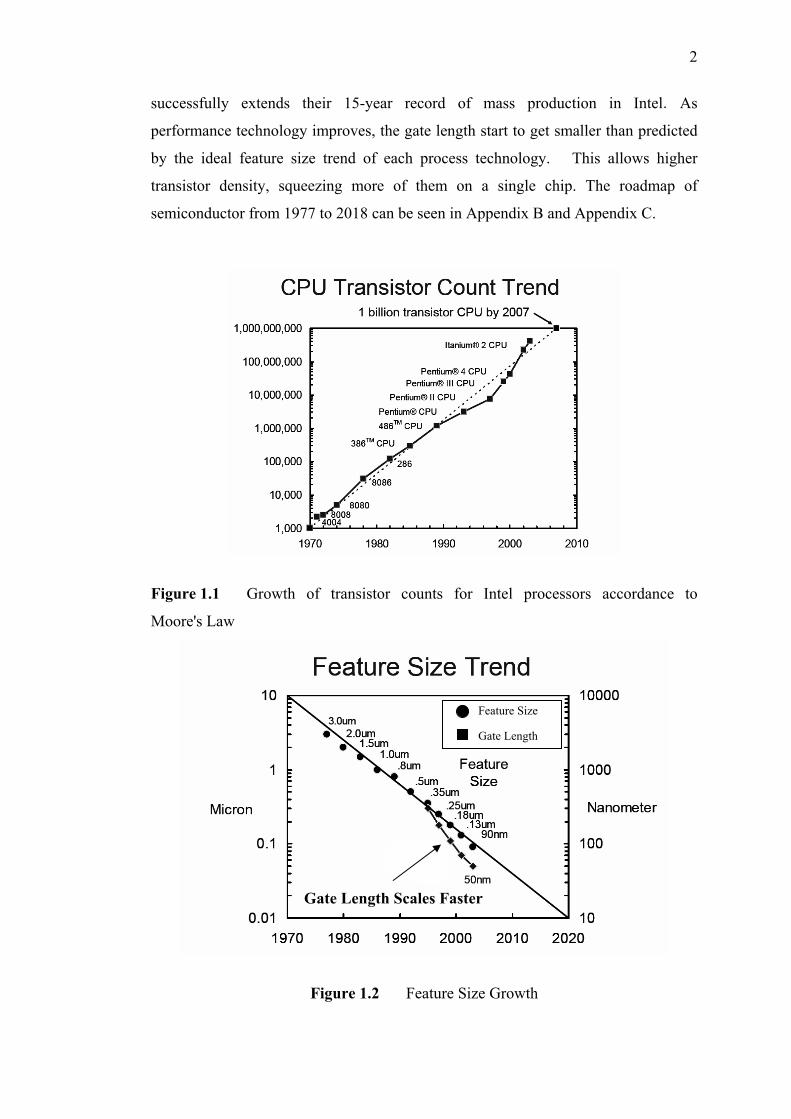
2
successfully extends their 15-year record of mass production in Intel. As
performance technology improves, the gate length start to get smaller than predicted
by the ideal feature size trend of each process technology. This allows higher
transistor density, squeezing more of them on a single chip. The roadmap of
semiconductor from 1977 to 2018 can be seen in Appendix B and Appendix C.
Figure 1.1 Growth of transistor counts for Intel processors accordance to
Moore's Law
Figure 1.2 Feature Size Growth
Gate Length Scales Faster
Feature Size
Gate Length
3
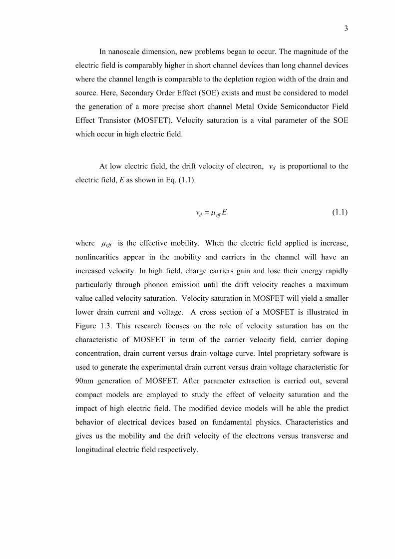
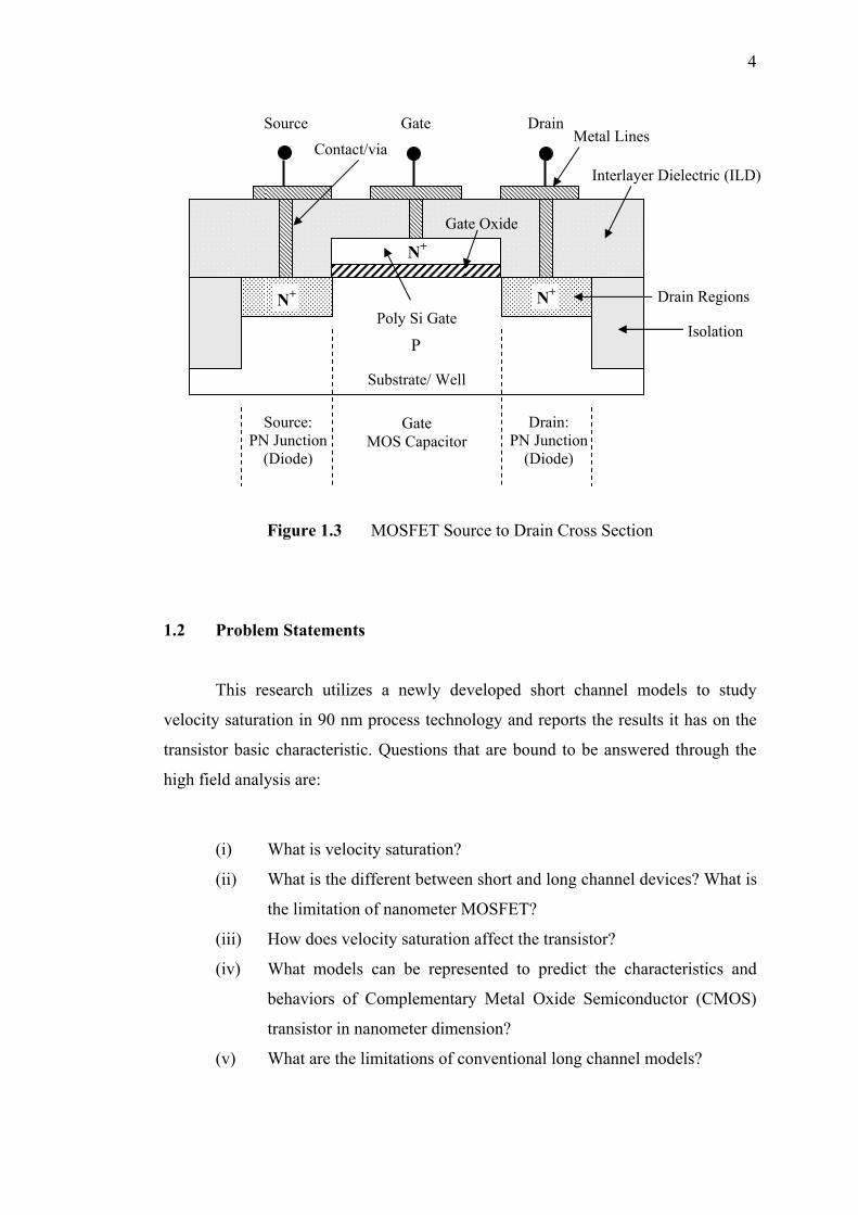
In nanoscale dimension, new problems began to occur. The magnitude of the
electric field is comparably higher in short channel devices than long channel devices
where the channel length is comparable to the depletion region width of the drain and
source. Here, Secondary Order Effect (SOE) exists and must be considered to model
the generation of a more precise short channel Metal Oxide Semiconductor Field
Effect Transistor (MOSFET). Velocity saturation is a vital parameter of the SOE
which occur in high electric field.
At low electric field, the drift velocity of electron, vd is proportional to the
electric field, E as shown in Eq. (1.1).
d effv Eμ= (1.1) where µeff is the effective mobility. When the electric field applied is increase,
nonlinearities appear in the mobility and carriers in the channel will have an
increased velocity. In high field, charge carriers gain and lose their energy rapidly
particularly through phonon emission until the drift velocity reaches a maximum
value called velocity saturation. Velocity saturation in MOSFET will yield a smaller
lower drain current and voltage. A cross section of a MOSFET is illustrated in
Figure 1.3. This research focuses on the role of velocity saturation has on the
characteristic of MOSFET in term of the carrier velocity field, carrier doping
concentration, drain current versus drain voltage curve. Intel proprietary software is
used to generate the experimental drain current versus drain voltage characteristic for
90nm generation of MOSFET. After parameter extraction is carried out, several
compact models are employed to study the effect of velocity saturation and the
impact of high electric field. The modified device models will be able the predict
behavior of electrical devices based on fundamental physics. Characteristics and
gives us the mobility and the drift velocity of the electrons versus transverse and
longitudinal electric field respectively.
4
Figure 1.3 MOSFET Source to Drain Cross Section
1.2 Problem Statements
This research utilizes a newly developed short channel models to study
velocity saturation in 90 nm process technology and reports the results it has on the
transistor basic characteristic. Questions that are bound to be answered through the
high field analysis are:
(i) What is velocity saturation?
(ii) What is the different between short and long channel devices? What is
the limitation of nanometer MOSFET?
(iii) How does velocity saturation affect the transistor?
(iv) What models can be represented to predict the characteristics and
behaviors of Complementary Metal Oxide Semiconductor (CMOS)
transistor in nanometer dimension?
(v) What are the limitations of conventional long channel models?
P
Source Gate Drain Metal Lines
Gate Oxide
Poly Si Gate
Interlayer Dielectric (ILD) Contact/via
Isolation
Substrate/ Well
Gate MOS Capacitor
Drain Regions
N+
Drain: PN Junction
(Diode)
Source: PN Junction
(Diode)
N+ N+
5
1.3 Objectives The following are the objectives of this study.
(i) To understand high field effects in nanoscale transistor in 90nm
process technology.
(ii) To formulate simple analytical and semi-empirical equations for
device model applicable to nanoscale devices by taking into account
velocity saturation.
(iii) To analyze velocity saturation effects on temperature, doping
concentration, longitudinal and transverse electric field.
1.4 Research Scope
The goal of this research is to investigate the role and characteristic of
velocity saturation on the following parameters.
(i) Longitudinal electric field
(ii) Transverse electric field
(iii) Doping concentration
(iv) Mobility
(v) Drain current and voltage (I-V) curve
(vi) Temperature
The research is divided into three major phases. In the beginning, literature
review and previous researches in this field is carried out. Strengths and weaknesses
of available model and equations are compared. The second phase begins with the
modeling based on the literature review. A semi-empirical model for velocity
saturation due to high field mobility degradation is presented. Best fit model
parameters are extracted from the experimental results. The results compared with a

6
set of published experimental data points and validated. The final phase is preceded
with analysis incorporating all the derived and modified models.
Future improvements and suggestion for the model are presented at the end of
the thesis. N-channel MOSFET with polysilicon gate is used in this research. The
Ids compact model is derived by studying and analyzing Berkeley Short-Channel
IGFET Model 3 Version 3 (BSIM3v3) standard (Berkeley, 2005). The one region
equation from linear to saturation is based on the modification of the conventional
long channel model with the addition of second order effects, each parameter with its
physical meanings. Other semi empirical models include threshold voltage, mobility
and source drain series resistance.
1.5 Contributions
The semiconductor industry particularly microchip industry strives to develop
high performance processor which is capable to cater for the demanding market.
MOSFET-based integrated circuits have become the dominant driving force in the
industry. It is important for the research and development’s designer team to
investigate how transistor behaves differently in nanometer dimension. These
characteristic includes the electric field, carrier velocity field, carrier mobility, carrier
concentration, carrier in saturation velocity region and drain current versus drain
voltage in short channel devices.
The modified short channel models are able to overcome the limitations of
previously long channel analytical and semi empirical models without velocity
saturation. It is also the interest of this study to find out the critical voltage and
electric field when velocity saturation appears. Based on this evaluation, it can
provide a guideline for designers in term of graphical representation on figures and
as well as parameter dependency relationship on the mobility behaviour, including
threshold voltage, doping concentration and temperature. Designer can examine the
behavior of the device when it is saturated at high electric field under specific
7
temperature and doping concentration. They can improve their design after a
thorough testing to prevent device breakdown.
Long channel I-V (current voltage) model is based on one dimensional
theory. The modified short channel model is more accurate for nanoscale MOSFET
than long channel model which cover Poisson's equation using gradual channel
approximation and coherent Quasi 2 Dimensional (2D) analysis in the velocity
saturation region. We have included the drain source resistance as well as the high
longitudinal electric field effects into the I-V model. Furthermore, the threshold
voltage model also includes the aspect of non ideal effects such as short channel
threshold voltage shift and narrow width effects. In addition, through these calculated
results, a bigger picture is given on how velocity saturation can be sustained. On top
of that, several enhancement and insight is discussed to overcome the challenges in
MOSFET design particularly the reduced drive strength. By investigating the effects
of velocity saturation, the author attempts to give general guidelines of how
parameters should be chosen.
1.6 Thesis Organization
This thesis consists of 8 chapters. Chapter 1 introduces the background of this
research. The problem statements, research objectives, research scope, research
contributions and thesis organization are also provided. Chapter 2 provides an
overview of the literatures reviewed throughout the research. A detailed description
on velocity saturation effects is presented. Previous long channel model
characteristics and related research are summarized.
Chapter 3 deals with the work flow of this research. It also introduce the
modeling process as well as the Intel Proprietary Schematic Editor and Circuit
Simulator. Chapter 4 marks the beginning of the proposed models formulation with
the introduction of threshold voltage modeling. Chapter 5 discusses about the
electron mobility model in MOS inversion layer. A comprehensive semi empirical
8
drain current and voltage model is explained in Chapter 6 by studying the long
channel characteristics and short channel effects. In addition, this chapter also
includes the derivation of source and drain resistance equation which normally
omitted in long channel devices. In Chapter 7, we study the velocity field model
which describes the effects of high vertical and lateral field in inversion layer pinch
off and velocity saturation.
In Chapter 8, the calculated data is observed and validated against the
experimental data generated from simulations to investigate effects of velocity
saturation. Analysis was carried out on the simulated results and the findings are
discussed. Finally, Chapter 9 concludes the thesis with summary of contributions and
suggestions for possible future development.

84
Several newly developed models are modified and employed to analyze the
characteristics and behaviors of transistor in sub-100 nm. They are the threshold
voltage model, physically based model for effective mobility and compact I-V,
velocity field model and source drain resistance model. It is vital to investigate the
physical insight into the device’s operating principles at high field to diminish hot
carrier effect and avoid catastrophic breakdown of the device via punchthrough. The
abovementioned models are improvement upon existing long channel models and
include various effects discussed in previous chapters.
Intel Proprietary Schematic Editor and Circuit Simulator are used to generate
experimental data. The relevant parameters are then extracted from the I-V curve.
Finally, the modified models are utilized to characterize the effects of velocity
saturation and effective mobility on drain voltage, gate voltage, temperature and
doping concentration. Simulated results show that the temperature effect on velocity
saturation depends on the predominant scattering mode. It is shown that at high fields
where surface roughness is predominant, the mobility has a negative temperature
coefficient and the velocity saturates at lower temperatures. Substrate doping
concentration changes the transverse field and scattering modes for a given gate bias,
and hence the saturation velocity is achieved at different longitudinal fields
9.2 Recommendations for Future Work
(i) The VT model can be modified to account for nonuniform channel
doping profile. When the MOSFET channel is nonuniformly doped,
designer has the flexibility to tailor the desired threshold voltage and
the off current requirement. Among the advanced MOSFET variation
is threshold voltage adjustment implantation, punchthrough
implantation and halo implantation.
(ii) The electron mobility model can be extended into strained and doped
silicon transport. The presence of a Ge alloy in strained silicon has
additional implications for the effective mobility over the universal
85
mobility curve. Alloy scattering can be added describe the carrier
collision with the SiGe alloy substrate.
(iii) The implication of velocity saturation effects on PMOS can also be
examined. With the simulated results, research can be carried out in
order to observe the hot carrier effects focusing on CMOS in
processor particularly at high temperature operation.
(iv) By using PSpice Model Editor, the derived model can be exported to
the library and configured to simulate the design output for DC
analysis. Instead of using Microsoft Excel, the analytical and semi
empirical models can be redefined into SPICE models and added into
a circuit as a schematic symbol to perform basic simulation.
REFERENCES
Agnello, P. D. (2002). Process requirements for continued scaling of CMOS - the
need and prospects for atomic-level manipulation. IBM J. Res. & Dev.
46(2/3):317-338.
Arora, V. K. (1989). Role of velocity. saturation in lifting pinchoff condition in long
channel MOSFET. IEEE Electronics Letter. 1989. 25(13):820-821.
Arora, V. K. (2000). Quantum Engineering of Nanoelectronic Devices.
Proceedings of the 22nd International Conference on Microelectronics
(MIEL2000), May 14-17, 2000. Nis, Serbia: IEEE. 2000. 19-27.
Arora, V. K. (2000). High-Field Effects in Sub-Micron Devices. IEEE Proceedings
Conference on Optoelectronic and Microelectronic Materials and Devices
(COMMAD), Dec 6-8, 2000. Brisbane, Australia: IEEE. 2000. 33-40.
Aslam, M., Artz, B. E., Kaberline, S. L. and Prater, T. J. (1993). A comparison of
cleaning procedures for removing potassium fromwafers exposed to KOH.
IEEE Transactions on Electron Devices. 40(2):292-295
Assaderaghi, F., Ko, P. K. and Hu, C. (1993). Observation of velocity overshoot in
silicon inversion layers. IEEE Electron Device Letter. 14(10):484-486.
Berkeley, University of California. BSIM3v3.3.0 MOSFET Model - Users' Manual.
California. V3.3. 2005.
Bringuier, E. (2002). On high-field departures from Ohm's local law.
Europe Journal of Physics. 23(3):367-370.
Codella, C.F. and Ogura, S. (1985). Halo doping effects in submicron DI-LDD
device design. International Electron Devices Meeting. 31:230-233.
Constant, I., Tardiff, F., Ardiff, F., and Derrien, J. (2000). Deposition and removal of
sodium contamination on silicon wafers. Semiconductor Science and
Technology. 15:61-66.

87
Dhar, S., Kosina, H., Palankovski, V., Ungersboeck, S.E., Selberherr, S. (2005).
Electron mobility model for strained-Si devices. IEEE Transactions on
Electron Device. 52(4):527-533.
Duheon, S., Junhee, L. and Kyungho, L. Device reliability and optimization on halo
MOSFETs. Proceedings of the 1995 IEEE International Symposium on
Reliability Physics. April 4-6, 1995. Las Vegas, Nevada: IEEE. 1995. 271-
275.
Frank, D. J., Dennard, R. H., Nowak, E., Solomon, P. M., Taur, Y. and Wong, H.-S.
P. (2001). Device Scaling Limits of Si MOSFETs and Their Application
Dependencies. Proceedings of the IEEE. 89:259-288.
Gamiz, F., Lopez-Villanueva, J. A., Banqueri, J., Carceller, J. E. and Cartujo, P.
(1995). Universality of electron mobility curves in MOSFETs: A Monte
Carlo study. IEEE Transactions on Electron Devices. 42(2):258-265.
Ghani, T., Armstrong, M., Auth, C., Bost, M., Charvat, P., Glass, G., Hoffmann, T.,
Johnson, K., Kenyon, C., Klaus, J., McIntyre, B., Mistry, K., Murthy, A.,
Sandford, J., Silberstein, M., Sivakumar, S., Smith, P., Zawadzki, K.,
Thompson, S., Bohr, M. (2003). A 90nm High Volume Manufacturing Logic
Technology Featuring Novel 45nm Gate Length Strained Silicon CMOS
Transistors. IEEE Electron Devices Meeting.:11.6.1-11.6.3.
Goo, J.-S., Qi Xiang, Takamura, Y., Haihong Wang, Pan, J., Arasnia, F., Paton, E.N.,
Besser, P., Sidorov, M.V., Adem, E., Lochtefeld, A., Braithwaite, G., Currie,
M.T., Hammond, R., Bulsara, M.T., Ming-Ren Lin (2003). Scalability of
strained-Si nMOSFETs down to 25 nm gate length. IEEE Electron Device
Letter. 24(5): 351-353.
Hauser, J. R. (1996). Extraction of experimental mobility data for MOS devices.
IEEE Transactions Electron Devices. 43(11):1981-1988.
Hu, C. (1993). Future CMOS scaling and reliability. Proceedings of the IEEE,
81(4):682-689.
Jeng, M., Ko, P. K. and Hu, C. (1988). A deep-submicrometer MOSFET model for
analog/digital circuit simulations. Electron Devices Meeting Intern. Tech.
Digest. 1:114-117.
Kahng, D. and Atalla, M. M. (1960). Silicon-silicon dioxide field induced surface
devices. IRE-AIEE Solid-State Device Research Conference, Carnegie
Institute of Technology, Pittsburgh, USA.
88
Ko, P. K. (1989). Approaches to scaling. Advanced MOS Device Physics. 18(1):1-37.
Lilienfeld, J. E. (1930). Method and apparatus for controlling electric currents.
US patent 1745175.
Lilienfeld, J. E. (1933). Device for controlling electric current.
US Patent 1745175.
Lim, K. Y. and Zhou, X. (2001). A physically-based semi-empirical effective
mobility model for MOSFET compact I–V modeling,” Solid-State Electron,
45(1):193-197.
Lochtefeld, A., Djomehri, I. J., Samudra G. and Antoniadis, D. A. (2002). New
insights into carrier transport in n-MOSFETs. IBM J. Res. & Dev.
46(2/3):347-358.
Moll, J. L. (1959). Variable capacitance with large capacity charge.
Wescon Convention Record. 3:32.
Moore, G. E. (1998). Cramming more components into integrated circuits
Proceedings of the IEEE. 86(1):82-85.
Neamen D. A. Semiconductor Physics and Devices. 3th Edition. McGraw-Hill
Higher Education :McGraw-Hill Companies. 2003. 537-542.
Ng, K. K. and Lynch,W. T. (1986). Analysis of the gate-voltage-dependent
series resistance of MOSFETs. IEEE Transactions on Electron Device.
33:965-972.
Ogura, S., Codella, C.F., Rovedo, N., Shepard, J.F. and Riseman, J. (1982). A half
micron MOSFET using double implanted LDD. International Electron
Devices Meeting. 28:718-721.
Pattanaik, M. and Banerjee, S. (2003). A new approach to model I-V characteristics
for nanoscale MOSFETs. VLSI Technology, Systems, and Applications 2003
International Symposium. 1:92-95.
Roldan, J. B., Gamiz, F., Lopez-Villanueva, J. A. and Carceller, J. E (1997).
Modeling Effects of Electron-Velocity Overshoot in a MOSFET
IEEE Transactions on Electron Devices. 44(5):841-846.
Sabnis, A. G. and Clemens, J. T. (1979). Characterization of the electron mobility in
the inverted <100> Si surface. IEDM Tech. Dig. 1:18-21.
Schwarz, S. A. and Russek, S. E. (1983). Semi-empirical equations for electron
velocity in silicon: Part II—MOS inversion layer. IEEE Trans. Electron
Devices. 30(12):1634-1639.

89
Sheu, B. J., Scharfetter, D. L., Ko, P. K. and Teng, M. C. (1987). BSIM: Berkeley
short-channel IGFET model for MOS transistors. IEEE Journal of Solid State
Circuits. 22(4):558-566
Shin, H., Yeric, G. M., Tasch, A. F. and Maziar, C. M. (1991). Physically-based
Models for Effective Mobility and Local Field Mobility of Electrons in MOS
Inversion Layers. Solid-State Electron. 34(6):545-552.
Skotnicki, T., Hutchby, J.A., Tsu-Jae King, Wong, H.-S.P., and Boeuf, F. (2005).
The end of CMOS scaling: toward the introduction of new materials and
structural changes to improve MOSFET performance. IEEE Circuits and
Devices Magazine. 21(1):16-26.
Sze, S. M. Physics of Semiconductor Devices, 2nd Edition. New York: John Wiley
and Sons Inc. 1981.
Sze, S. M. Semiconductor Devices: Physics and Technology. 2nd Edition. New York
:John Wiley and Sons Inc. 2002.
Takeuchi, K. and Fukuma, M. (1994). Effects of the velocity saturated region on
MOSFET characteristics. IEEE Transactions on Electron Devices.
41:1623-1627.
Taur, Y., Buchanan, D. A., Chen, W., Frank, D. J., Ismail, K. E., Lo, S.-H., Sai-
Halasz, G. A., Viswanathan, R. G., Wann, H.-J. C., Wind, S. J. and Wong,
H.-S. (1997). CMOS Scaling into the Nanometer Regime. Proceedings of the
IEEE, 85:486-504
Taur, Y. (2002). CMOS Design Near the Limit of Scaling. IBM J. Res. & Dev., vol.
46(2/3):213-222.
Taur, Y. and Ning, T. H. Semiconductor Physics and Devices. 6th Edition. The Piyy
Building, Trumpington Street :Cambridge University Press. 2002.
Thompson, S.E., Armstrong, M., Auth, C., Alavi, M., Buehler, M., Chau, R., Cea, S.,
Ghani, T., Glass, G., Hoffman, T., Jan, C.-H., Kenyon, C., Klaus, J., Kuhn,
K., Zhiyong Ma, Mcintyre, B., Mistry, K., Murthy, A., Obradovic, B.,
Nagisetty, R., Phi Nguyen, Sivakumar, S., Shaheed, R., Shifren, L., Tufts, B.,
Tyagi, S., Bohr, M., El-Mansy, Y. (2004). A 90-nm logic technology
featuring strained-silicon. IEEE Transactions on Electron Device.
51(11):1790-1797.

90
Thompson, S.E., Armstrong, M., Auth, C., Cea, S., Chau, R., Glass, G., Hoffman, T.,
Klaus, J., Zhiyong Ma, Mcintyre, B., Murthy, A., Obradovic, B., Shifren, L.,
Sivakumar, S., Tyagi, S., Ghani, T., Mistry, K., Bohr, M., El-Mansy, Y.
(2004). A logic nanotechnology featuring strained-silicon. IEEE Electron
Device Letter. 25(4):191-193.
Trofinenkoff, F. N. (1965). Field dependent mobility analysis of the field effect
transistor. Proceedings of the IEEE, 53:1765.
Tsividis, Y. Operation and Modeling of The MOS Transistor. 2nd Edition. Madison
Avenue, New York :Oxford University Press Inc. 1999.
Wang, R., Dudley, J., DeMassa, T. A. and Jelsma, L. F. (1971). Threshold voltage
variations with temperature in MOS transistors. IEEE Trans. Electron
Devices. 18:386-388.
Wolf, S. Silicon Processing For The VLSI Era Volume 3: The Submicron MOSFET.
Sunset Beach, California :Lattice Press. 1995.
Xuemei, X., and Mohan, D. (2006). BSIM3 homepage.
http://www-device.eecs.berkeley.edu/~bsim3/latenews.html
BSIM Research Group.
Yu, B., Wann, C. H. J., Nowak, E. D., Noda, K. and Hu, C. (1997). Short-channel
effect improved by lateral channel-engineering in deep-submicrometer
MOSFET’s. IEEE Trans. Electron Devices. 44:627-633
Yu, Z., Shao, X., Zhang, D. and Tian L. Quantum Mechanical Carrier Transport and
Nano-scale MOS Modeling. Institute of Microelectronics, Tsinghua
University, Beijing 100084, China.
Zeghbroeck, B. V. (2004). Principles of Semiconductor Devices.
http://ece-www.colorado.edu/~bart/book/book/chapter2/ch2_3.htm#tab2_3.
Zeitzoff, P.M. (2004). Challenges and key potential technological innovations for
scaling MOSFETS through the end of the roadmap. International Conference
on Solid-State and Integrated Circuits Technology Proceedings. Oct. 18-21,
2004. Austin, Texas. IEEE. 2004. 20-25.
Zeitzoff, P.M. and Chung, J.E. (2005). A perspective from the 2003 ITRS: MOSFET
scaling trends, challenges, and potential solutions. IEEE Circuits and
Devices Magazine. 21(1):4-15.
91
Zhou, X., Lim, K. Y. and Lim D. (1999). A simple and unambiguous definition of
threshold voltage and its implications in deep-submicron MOS device
modeling. IEEE Trans. Electron Devices. 46(4):807-809.
Zhou, X. and Lim, K. Y. (2000). Physically-based semi-empirical series resistance
model for deep-submicron MOSFET I-V modeling. IEEE Transactions on
Electron Devices. 47(6):1300-1302.
Zhou, X. and Lim, K. Y. (2001). Unified MOSFET compact I-V model formulation
through physics-based effective transformation. IEEE Transactions on
Electron Device. 48(5):887-896.


