31
Micro-fabrication
| Date post: | 26-Dec-2015 |
| Category: |
Documents |
| Upload: | charlotte-parks |
| View: | 232 times |
| Download: | 3 times |

Micro-fabrication

Photolithography-Outline
History Methods and Theories of Photolithography Preparation and Priming Spin-Coating Photoresists Soft-baking Mask Alignment and Exposure Developing Hard-baking

History Historically, lithography is a type of printing technology
that is based on the chemical repellence of oil and water. Photo-litho-graphy: latin: light-stone-writing In 1826, Joseph Nicephore Niepce, in Chalon, France,
takes the first photograph using bitumen of Judea on a pewter plate, developed using oil of lavender and mineral spirits
In 1935 Louis Minsk of Eastman Kodak developed the first negative photoresist
In 1940 Otto Suess developed the first positive photoresist. In 1954, Louis Plambeck, Jr., of Du Pont, develops the
Dycryl polymeric letterpress plate

Photolithography In photolithography, the pattern is created
photographically on a substrate (silicon wafer) Photolithography is a binary pattern transfer: there is
no gray-scale, color, nor depth to the image This pattern can be used as a resist to substrate
etchant, or a mold, and other forms of design processes
The steps involved are wafer cleaning, photoresist application, soft baking, mask alignment, and exposure and development

Preparation and Priming Prepare the substrate :
Wash with appropriate solvent to remove any matter and other impurities
TCE, Acetone, MeOH Dry in Oven at 150°C for 10 min. Place on hotplate and cover with petri dish, let temp.
stabilize at 115°C. Deposit Primer (optional)
Chemical that coats the substrate and allows for better adhesion of the resist
TCE = trichloroethylene, MeOH = methanol

Spin-Coating the Resist
Spin on the photoresist to the suface of the wafer
Standard methods are to use high spin coaters
rpm:
Time:
Produces a thin uniform layer of photoresist on the wafer surface.
Exposure
Use UV light at this stage

Photoresist
Photoresist is an organic polymer which changes its chemical structure when exposed to ultraviolet (UV) light.
It contains a light-sensitive substance whose properties allow image transfer onto a printed circuit board.
There are two types of photoresist: positive and negative

Positive/negative resist

Diagram:
Exposure to UV light makes it more soluble in the developer
Exposed resist is washed away by developer so that the unexposed substrate remains
Results in an exact copy of the original design
Exposure to UV light causes the resist to polymerize, and thus be more difficult to dissolve
Developer removes the unexposed resist
This is like a photographic negative of the pattern

Soft-Baking Put on hotplate, or in oven
Temperature ; Time Removes volatile solvents from the coating Makes photoresist non-sticky
Hardens to amorphous solid Be careful not to over bake and destroy the
sensitizer

Masking and Exposure

Mask fabrication process

Mask Alignment and Exposure
Photomask is a square glass plate with a patterned emulsion of metal film on one side
After alignment, the photoresist is exposed to UV light
Three primary exposure methods: contact, proximity, and projection

Exposure Methods

Photoresist Developer
Highly-pure buffered alkaline solution Removes proper layer of photoresist upon contact
or immersion Degree of exposure affects the resolution curves
of the resist

Hard Baking
Final step in the photolithographic process Not always necessary; depends on the
resist Hardens the photoresist Improves adhesion of the photoresist to the
wafer surface

Etching
Etching type
Wet etching
Dry etching Etching steps
Oxidation
Reaction
Remove products

Factors in Wet Etching
Limited • Reaction limited • Diffusion limited • Factors • Concentration • Temperature • Stirring

HNA mixture of nitric (HNO3), hydrofluoric (HF) and acetic
(CH3COOH) acids HNO3 oxides Si, HF removes SiO2, repeat…
high HNO3:HF ratio (etch limited by oxide removal) low HNO3:HF ratio (etch limited by oxide formation) dilute with water or acetic acid (CH3COOH) acetic acid is preferred because it prevents HNO3 dissociation
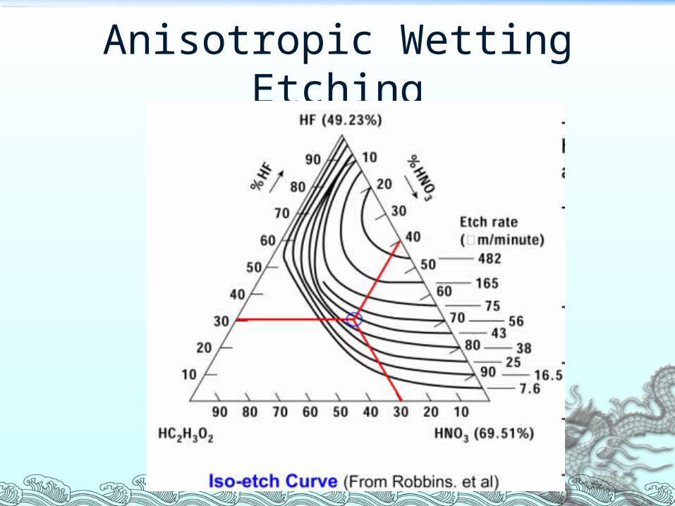
Anisotropic Wetting Etching

Anisotropic Etch

Anisotropic Etchants
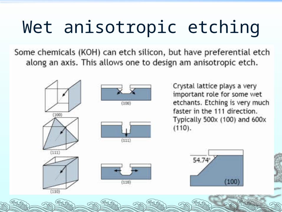
Wet anisotropic etching

Etch the material

Wet Etching vs Dry Etching

Etch Mechanism

Gas Phase Etch

RF-Plasma-Based Dry Etching

Dry Etch Chemistries

Methods of Dry Etching

Types of Dry Etching Processes


