Microstructure of diamond and βSiC interlayer studied by s ynchrotron xray scattering J. H. Je and D. Y. NohCitation: J. Appl. Phys. 80 , 2791 (1996); doi: 10.1063/1.363197 View online: http://dx.doi.org/10.1063/1.363197 View Table of Contents: http://jap.aip.org/resource/1/JAPIAU/v80/i5 Published by theAmerican Instit ute of Physics. Related Articles FeNi-based magnetoimpedance multilayers: Tailoring of the softness by magnetic spacers Appl. Phys. Lett. 100, 162410 (2012) Optical dielectric behaviors of copper zinc alloy thin films J. Appl. Phys. 111, 073103 (2012)Effect of Si interlayers on the magnetic and mechanical properties of Fe/Ge neutron polarizing multilayer mirrors J. Appl. Phys. 111, 063904 (2012)Chemical vapor deposition of polycrystalline Fe3O4 thin films by using the cyclohexadiene iron tricarbonyl liquid precursorJ. Appl. Phys. 111, 07B107 (2012)Columnar grain growth of FePt(L10) thin filmsJ. Appl. Phys. 111, 07B720 (2012)Additional information on J. Appl. Phys. Journal Homepage: http://jap.aip.org/ Journal Information: http://jap.aip.org/about/about_the_journal Top downloads: http://jap.aip.org/features/most_downloaded Information for Authors: http://jap.aip.org/authors Downloaded 24 Apr 2012 to 200.136.236.102. Redistribution subject to AIP license or copyright; see http://jap.aip.org/about/rights_and _permissions
Transcript
8/2/2019 Micro Structure of Diamond and SiC Inter Layer Studied by Synchrontron Xray Scattering
Microstructure of diamond and βSiC interlayer studied by synchrotron xrayscatteringJ. H. Je and D. Y. Noh Citation: J. Appl. Phys. 80, 2791 (1996); doi: 10.1063/1.363197 View online: http://dx.doi.org/10.1063/1.363197 View Table of Contents: http://jap.aip.org/resource/1/JAPIAU/v80/i5 Published by the American Institute of Physics. Related Articles
FeNi-based magnetoimpedance multilayers: Tailoring of the softness by magnetic spacers Appl. Phys. Lett. 100, 162410 (2012) Optical dielectric behaviors of copper zinc alloy thin films J. Appl. Phys. 111, 073103 (2012) Effect of Si interlayers on the magnetic and mechanical properties of Fe/Ge neutron polarizing multilayer mirrors J. Appl. Phys. 111, 063904 (2012) Chemical vapor deposition of polycrystalline Fe3O4 thin films by using the cyclohexadiene iron tricarbonyl liquidprecursor J. Appl. Phys. 111, 07B107 (2012) Columnar grain growth of FePt(L10) thin films J. Appl. Phys. 111, 07B720 (2012) Additional information on J. Appl. Phys.
Journal Homepage: http://jap.aip.org/ Journal Information: http://jap.aip.org/about/about_the_journal Top downloads: http://jap.aip.org/features/most_downloaded Information for Authors: http://jap.aip.org/authors
Downloaded 24 Apr 2012 to 200.136.236.102. Redistribution subject to AIP license or copyright; see http://jap.aip.org/about/rights_and_permissions
Diamond films, grown by chemical vapor depositionCVD, have great potential applications due to the excellentand unique properties of diamond. Potential electronic de-vices utilizing diamond films are those operating under highpower, high frequency, high temperatures, chemically harsh,and high radiation flux environments. For these applications,single crystal diamonds grown on economically viable sub-strates are preferred. Two-dimensional heteroepitaxialgrowth of diamond films, however, has not been very fruitfulyet even with the continuous improvement of diamond
growth techniques.1– 7
The high surface energy8
and thesmall interatomic spacing of diamond prevent the formationof high quality heteroepitaxial films on foreign substrates. Inaddition, the large lattice mismatch between diamond andconventional substrates increases the misfit, and the strainenergy at the interface substantially, which enhances the ten-dency toward three-dimensional island growth.
The understanding of the nucleation mechanism of dia-mond under CVD conditions is rather limited. To reveal thenucleation mechanism, it is essential to study the microstruc-ture of the diamond and the interface between the diamondand the substrates. Several studied using high resolutiontransmission electron microscopy TEM reported observa-
tions of -SiC layer formed as an interfacial layer in theprocess of growing diamond using microwave plasmachemical vapor deposition MPCVD.9–17 It is essential tostudy the nature of the -SiC interlayer thus formed, to un-derstand the growth mechanism of diamond particles. Al-though most of the studies show nonepitaxial island growthof diamond, there are a few results that show limited evi-dence of local epitaxy of the diamond on the interfacial sili-con carbide layer.9–15 However, it seems far from satisfac-
tory to draw any statistically meaningful conclusions of theheteroepitaxy of diamond on the SiC interlayer with only theTEM observations that provide only the local microstructuralinformation.
In this article, we report a synchrotron x-ray scatteringstudy of the microstructure of the diamond particles and theSiC interlayer. Synchrotron radiation with very high flux isone of the best probes for characterizing structural propertiesof ultra thin films such as the SiC interlayer. Since x rayspenetrate more than a few micrometers in most materials,microstructure of both the diamond particles and of the in-
terface can be studied simultaneously and nondestructively.It is also well known that x-ray scattering provides atomicscale information that is statistically averaged over macro-scopic illuminated area of order a few mm2. The dependenceof the structure of the SiC interlayer on the deposition con-ditions, and the orientational relationship between the dia-mond particle and the SiC interlayer were the main themesof this study. We also studied the effects of the substratepretreatment, of the deposition time, and of the substrateorientation on the growth of diamond and of the SiC inter-layer.
This article is organized as follows. In Sec. II, we de-scribe the experimental details including the film growthconditions and the x-ray scattering measurement setup. Inaddition to the conventional powder diffraction method, wedescribed a few new scanning paths of the scattering profilethat are useful in studying the film-substrate epitaxial rela-tionship. In Sec. III, we discuss the microstructure of the SiCinterlayer, and the epitaxial relation between the SiC inter-layer and the substrates. In Sec. IV, the structural informa-tion of the diamond particles is presented. In Sec. V, wesummarize the paper with concluding remarks.a
The diamonds were grown using the MPCVD techniquewhose details were reported previously.18 The depositionwas carried out under the condition of 2.0% methane in abalance of hydrogen keeping the total flow rate of 100 sccm,and the pressure of 30 Torr. The microwave power was fixedat 600 W, and the substrate temperature was 800 °C. Thesamples used in this study were prepared on four differentkinds of silicon substrates of 11 cm in size; the pretreated-Si111 Si111-PT, the pretreated-Si001 Si001-PT,the nontreated-Si111 Si111-NT, and the nontreated-Si001 Si001-NT. The pretreatment was carried out byultrasonically vibrating the substrates in an alcohol suspen-sion of 20–30 m diamond powder for 1 h followed byultrasonic cleaning in acetone for 30 min.
Figures 1a and 1b show the scanning electron micro-graphs of the diamonds grown under the conditions specified
above for 2 h on the Si111-PT and on the Si001-PT sub-strates, respectively. Diamond particles are clearly observedon both the substrates. The grains were about to merge eachother in about 2 h of deposition. When the deposition wasperformed for only 30 min on the Si111-PT substrate, thesize of the diamond particles was below 1 m. Meanwhile,on the Si111-NT and the Si001-NT substrates, the dia-mond particles were not observed within the resolving powerof the SEM up to 2 h of deposition. We note here that it wasnot possible to draw any conclusions on the orientationalrelationship of the diamond particles, or the existence of theinterfacial SiC layer with the SEM pictures.
B. X-ray scattering set up
The x-ray scattering experiments were carried out atBeamline X10B at National Synchrotron Light SourceNSLS at Brookhaven National Laboratory. The incidentx-rays were focused vertically by a focusing mirror. A hori-zontally bent Si111 crystal was used to monochromatize xrays to 11 keV wavelength of 1.1305 Å, and to focus themhorizontally as well. Typical momentum transfer resolutionwas controlled by two pairs of slits, and was set at 0.001Å1 in this experiment.
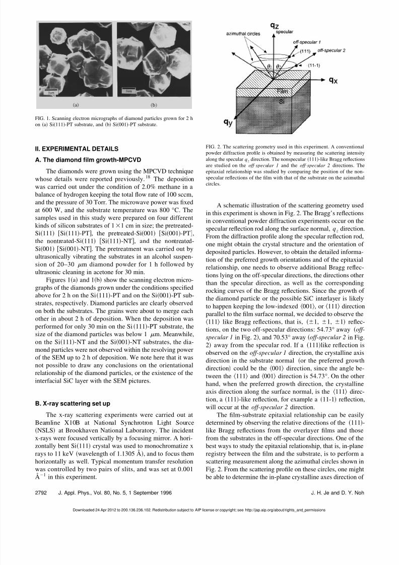
A schematic illustration of the scattering geometry usedin this experiment is shown in Fig. 2. The Bragg’s reflectionsin conventional powder diffraction experiments occur on thespecular reflection rod along the surface normal, q z direction.From the diffraction profile along the specular reflection rod,one might obtain the crystal structure and the orientation of deposited particles. However, to obtain the detailed informa-tion of the preferred growth orientations and of the epitaxialrelationship, one needs to observe additional Bragg reflec-tions lying on the off-specular directions, the directions otherthan the specular direction, as well as the correspondingrocking curves of the Bragg reflections. Since the growth of
the diamond particle or the possible SiC interlayer is likelyto happen keeping the low-indexed 001, or 111 directionparallel to the film surface normal, we decided to observe the111 like Bragg reflections, that is, 1, 1, 1 reflec-tions, on the two off-specular directions: 54.73° away off -specular 1 in Fig. 2, and 70.53° away off -specular 2 in Fig.2 away from the specular rod. If a 111like reflection isobserved on the off -specular 1 direction, the crystalline axisdirection in the substrate normal or the preferred growthdirection could be the 001 direction, since the angle be-tween the 111 and 001 direction is 54.73°. On the otherhand, when the preferred growth direction, the crystallineaxis direction along the surface normal, is the 111 direc-tion, a 111-like reflection, for example a 11-1 reflection,will occur at the off -specular 2 direction.
The film-substrate epitaxial relationship can be easilydetermined by observing the relative directions of the 111-like Bragg reflections from the overlayer films and thosefrom the substrates in the off-specular directions. One of thebest ways to study the epitaxial relationship, that is, in-planeregistry between the film and the substrate, is to perform ascattering measurement along the azimuthal circles shown inFig. 2. From the scattering profile on these circles, one mightbe able to determine the in-plane crystalline axes direction of
FIG. 1. Scanning electron micrographs of diamond particles grown for 2 hon a Si111-PT substrate, and b Si001-PT substrate.
FIG. 2. The scattering geometry used in this experiment. A conventionalpowder diffraction profile is obtained by measuring the scattering intensityalong the specular q z direction. The nonspecular 111-like Bragg reflectionsare studied on the off -specular 1 and the off -specular 2 directions. Theepitaxial relationship was studied by comparing the position of the non-specular reflections of the film with that of the substrate on the azimuthalcircles.
2792 J. Appl. Phys., Vol. 80, No. 5, 1 September 1996 J. H. Je and D. Y. Noh
Downloaded 24 Apr 2012 to 200.136.236.102. Redistribution subject to AIP license or copyright; see http://jap.aip.org/about/rights_and_permissions
8/2/2019 Micro Structure of Diamond and SiC Inter Layer Studied by Synchrontron Xray Scattering
the film relative to those of the substrate. We note that thepolar angle, the angle from the surface normal is alwaysfixed to be constant on the azimuthal circle. To achieve thecomplicated scattering geometry used in these experiments,we employed a four-circle x-ray diffractometer that enablesus to attain arbitrary momentum transfer q in three-dimensional space. The detailed scattering geometry using afour-circle diffractometer has been well described in Ref. 19.
III. MICROSTRUCTURE OF THE -SiC INTERLAYER
A. Powder diffraction pattern
To reveal the crystal structure of the overlayers depos-ited in the microwave plasma CVD process, we first carriedout the conventional powder diffraction measurement byvarying the momentum transfer q along the surface normal.The powder diffraction patterns obtained on the four differ-
ent kinds of substrates studied here are illustrated in Fig. 3.In addition to the Bragg reflection from diamond particles,that will be discussed in the following section, we foundintense Bragg reflections that occur at the positions of theBragg reflections of a -SiC crystal. This immediately tellsus that -SiC crystal was formed as an interlayer in theMPCVD process in agreement with the previously reportedcross-sectional TEM images of -SiC interlayers.9–15
We first discuss the diffraction profile of the samplesprepared on the Si111 substrates, both pretreated Fig. 3a
and nontreated Fig. 3b. As shown in the figure, the Braggreflection occurs at q z 2.505 Å1 that corresponds to theposition of -SiC111 reflection. This indicates that on theSi111 substrates the -SiC layer grows keeping the 111
crystal axis direction parallel to the surface normal. The pre-ferred growth direction, the crystalline axis direction that lieson the overall growth direction, in this case was the 111
direction. On the Si111-PT, the -SiC111 reflection wassharper and more intense than that on the Si111-NT sug-gesting that the growth rate of the -SiC was much higher onthe pretreated substrate. The pretreatment of the substrateenhanced the growth rate of the -SiC interlayer signifi-
cantly. We attribute the increase of the growth rate to thecreation of the nucleation sites by the pretreatment. The pre-treatment presumably creates various kinds of defects thatmight act as nucleation sites.20–29
From the broadening of the scattering profile, one mayestimate the crystal domain size of the -SiC interlayer thatwas limited by the presence of misfit dislocations or by thefinite film thickness. The crystal domain size l might be de-duced from the half-width at the half-maximum HWHM of the scattering profile by l /HWHM.30 In the Si111-PTsubstrate, the crystal domain size of the -SiC thus obtainedwere l 260 Å, and l 83 Å as deposited for 2 h and for30 min, respectively. These domain sizes calculated from the
specular reflection are likely to be limited by the finite thick-ness of the -SiC interlayer, therefore, we speculate that theyrepresent the thickness of the -SiC interlayer. From this, weconclude that the -SiC interlayer was grown further afterdeposition of 30 min. The integrated intensity of the -SiCreflection of the sample with 30 min deposition, that wasshown in Fig. 3a by solid squares or the dotted line in theinset of Fig. 3a, was also about three times lower than thatof the sample with 2 h of deposition. This also indicates thatthe -SiC interlayer was kept growing after 30 min of depo-sition. This fact is in striking contrast to the results of thespectroscopic ellipsometry data,31 and the transmission Fou-rier transform infrared FTIR32 data that suggested the -SiC interlayer reaches to an equilibrium thickness before30 min of deposition. On the Si111-NT, the HWHM of the -SiC111 was as broad as 0.075 Å1, and the calculatedthickness of the -SiC was only 42 Å.
On the other hand, the -SiC interlayer was grown pref-erentially along the 001 direction on the Si001 substrates.Figure 3c shows the powder diffraction profile of the -SiC/Si001-PT. In this case, the Bragg reflection occurs atq z 2.890 Å1corresponding to the -SiC 002 peak posi-tion. This indicates that the growth direction of the -SiCinterlayer was the 001 direction. Interestingly, the Bragg
FIG. 3. a Powder diffraction pattern of the sample prepared on theSi111-PT. The open circle is the data on the sample grown for 2 h, whilethe filled circle represents the data on the sample grown for 30 min. The
strong -SiC111 peak is rescaled in the inset figure. b Powder diffractionpattern of the sample grown on the Si111-NT for 2 h. Only the broad -SiC111 peak was observed, and no diamond peak was measured. cPowder diffraction pattern of the sample grown on the Si 001-PT for 2 h. Inthis case, the -SiC002 peak was obtained together with the diamond111 reflection. d Powder diffraction pattern of the sample grown on theSi001-NT for 2 h. No features of -SiC or of diamond were measurable.
2793J. Appl. Phys., Vol. 80, No. 5, 1 September 1996 J. H. Je and D. Y. Noh
Downloaded 24 Apr 2012 to 200.136.236.102. Redistribution subject to AIP license or copyright; see http://jap.aip.org/about/rights_and_permissions
8/2/2019 Micro Structure of Diamond and SiC Inter Layer Studied by Synchrontron Xray Scattering
reflection of the -SiC002 /Si001-PT was much weakerand broader than that of the -SiC111 /Si111-PT. The do-main size calculated from the HWHM of the -SiC002
reflection, 0.035 Å1 was about l 90 Å. The domain sizewas probably limited by the finite thickness of the -SiCinterlayer. On the Si001-NT substrate, there was no signa-ture of the -SiC interlayer in the scattering profile as shownin Fig. 3d. We believe that the amount of the nucleated -SiC interlayer was too small to be detected. From theseresults, we conclude that the nucleation of the -SiC inter-layer is easier on the Si111 substrates than on the Si001
substrates.
B. Epitaxial relation of the -SiC interlayer to thesilicon substrates
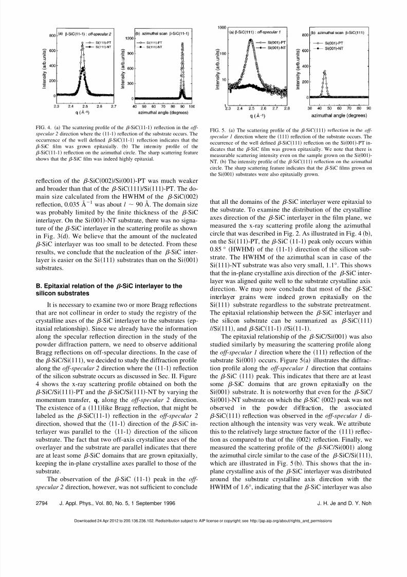
It is necessary to examine two or more Bragg reflectionsthat are not collinear in order to study the registry of thecrystalline axes of the -SiC interlayer to the substrates ep-itaxial relationship. Since we already have the informationalong the specular reflection direction in the study of thepowder diffraction pattern, we need to observe additionalBragg reflections on off-specular directions. In the case of the -SiC/Si111, we decided to study the diffraction profilealong the off -specular 2 direction where the 11-1 reflectionof the silicon substrate occurs as discussed in Sec. II. Figure4 shows the x-ray scattering profile obtained on both the -SiC/Si111-PT and the -SiC/Si111-NT by varying themomentum transfer, q, along the off -specular 2 direction.The existence of a 111like Bragg reflection, that might belabeled as the -SiC11-1 reflection in the off -specular 2
direction, showed that the 11-1 direction of the -SiC in-terlayer was parallel to the 11-1 direction of the siliconsubstrate. The fact that two off-axis crystalline axes of theoverlayer and the substrate are parallel indicates that thereare at least some -SiC domains that are grown epitaxially,keeping the in-plane crystalline axes parallel to those of thesubstrate.
The observation of the -SiC 11-1 peak in the off -specular 2 direction, however, was not sufficient to conclude
that all the domains of the -SiC interlayer were epitaxial tothe substrate. To examine the distribution of the crystallineaxes direction of the -SiC interlayer in the film plane, wemeasured the x-ray scattering profile along the azimuthalcircle that was described in Fig. 2. As illustrated in Fig. 4b,on the Si111-PT, the -SiC 11-1 peak only occurs within0.85 ° HWHM of the 11-1 direction of the silicon sub-strate. The HWHM of the azimuthal scan in case of theSi111-NT substrate was also very small, 1.1°. This showsthat the in-plane crystalline axis direction of the -SiC inter-layer was aligned quite well to the substrate crystalline axisdirection. We may now conclude that most of the -SiCinterlayer grains were indeed grown epitaxially on the
Si111 substrate regardless to the substrate pretreatment.The epitaxial relationship between the -SiC interlayer andthe silicon substrate can be summarized as -SiC111
//Si111, and -SiC11-1 //Si11-1.The epitaxial relationship of the -SiC/Si001 was also
studied similarly by measuring the scattering profile alongthe off -specular 1 direction where the 111 reflection of thesubstrate Si001 occurs. Figure 5a illustrates the diffrac-tion profile along the off -specular 1 direction that containsthe -SiC 111 peak. This indicates that there are at leastsome -SiC domains that are grown epitaxially on theSi001 substrate. It is noteworthy that even for the -SiC/ Si001-NT substrate on which the -SiC 002 peak was notobserved in the powder diffraction, the associated -SiC111 reflection was observed in the off -specular 1 di-rection although the intensity was very weak. We attributethis to the relatively large structure factor of the 111 reflec-tion as compared to that of the 002 reflection. Finally, wemeasured the scattering profile of the -SiC/Si001 alongthe azimuthal circle similar to the case of the -SiC/Si111,which are illustrated in Fig. 5b. This shows that the in-plane crystalline axis of the -SiC interlayer was distributedaround the substrate crystalline axis direction with theHWHM of 1.6°, indicating that the -SiC interlayer was also
FIG. 4. a The scattering profile of the -SiC11-1 reflection in the off -specular 2 direction where the 11-1 reflection of the substrate occurs. Theoccurrence of the well defined -SiC11-1 reflection indicates that the -SiC film was grown epitaxially. b The intensity profile of the -SiC11-1 reflection on the azimuthal circle. The sharp scattering featureshows that the -SiC film was indeed highly epitaxial.
FIG. 5. a The scattering profile of the -SiC111 reflection in the off -specular 1 direction where the 111 reflection of the substrate occurs. Theoccurrence of the well defined -SiC111 reflection on the Si001-PT in-dicates that the -SiC film was grown epitaxially. We note that there ismeasurable scattering intensity even on the sample grown on the Si001-NT. b The intensity profile of the -SiC111 reflection on the azimuthalcircle. The sharp scattering feature indicates that the -SiC films grown onthe Si001 substrates were also epitaxially grown.
2794 J. Appl. Phys., Vol. 80, No. 5, 1 September 1996 J. H. Je and D. Y. Noh
Downloaded 24 Apr 2012 to 200.136.236.102. Redistribution subject to AIP license or copyright; see http://jap.aip.org/about/rights_and_permissions
8/2/2019 Micro Structure of Diamond and SiC Inter Layer Studied by Synchrontron Xray Scattering
grown epitaxially on the Si001 substrate. The orientationrelationship of the epitaxially grown -SiC/Si001 canbe summarized as -SiC001 //Si001, and -SiC111
//Si111.In fact, it is rather surprising that the -SiC interlayer
was always grown epitaxially on the silicon substrates, eventhough the lattice mismatch is as large as 20% between the -SiC and the silicon substrates. From the broadening of thein-plane scattering profile, one might also estimate the crys-tal domain size of the -SiC interlayer in the film plane that
was limited only by the presence of misfit dislocations. Thein-plane domain size estimated from the in-plane scatteringprofile of -SiC/Si111-PT was 240 Å, and that of -SiC/ Si111-NT was 165 Å. These small domain sizes indicatethat there were a fair amount of misfit dislocations at theinterface between the -SiC and the substrates. The in-planedomain size -SiC/Si001-PT was even smaller, 85 Å. Wespeculate that the large lattice mismatch between the -SiCand the silicon was accommodated by the creation of a largenumber of misfit dislocations. The observation of the het-eroepitaxy of the -SiC interlayer has been reportedpreviously.33–37
C. Mosaic distribution of the preferred orientation
As the -SiC film grows, the crystalline axis direction of each grain may tilt away from the firm normal causing adistribution of the preferred growth direction. In this process,the interfacial strain caused by the large lattice mismatchcould be relaxed. The mosaic distribution of the crystallineaxis is usually studied by measuring the scattering intensityas the sample is rocked, while the magnitude of the momen-tum transfer is held at the position of a Bragg reflection. Fora single crystal, the rocking curve would be sharp -functionlike, while a complete powder specimen would show a con-stant intensity distribution.
Figures 6a and 6b show the rocking curves of the -SiC11-1 /Si111-PT and the -SiC 11-1 /Si111-NT,respectively. This shows that the crystalline axis in the out-of-plane direction of the -SiC interlayers grown on theSi111 substrates, were well aligned to the substrates crys-talline axis direction within 0.6° HWHM, Si111-PT,and 1.5° HWHM, Si111-NT. Meanwhile, on the -SiC111 /Si001-PT, the rocking curve of the Bragg re-flection on the off -specular 1 direction Fig. 6c shows mo-saic distribution with 1.5° HWHM. Interestingly, the mosaicdistribution of the -SiC002 /Si001-NT substrate wasrelatively small with 0.23° FWHM as illustrated in Fig.6d. This fact may be related with the small thickness of the
-SiC interlayer 25 Å grown on the Si001-NT sub-strate. We speculate that these mosaic structures of -SiCinterlayers were developed in the process of accommodatingthe large lattice mismatch during the growth.
IV. STRUCTURAL PROPERTIES OF DIAMONDPARTICLES
A. Diamond particles grown with the Š111‹ preferredgrowth orientation
The presence of diamond particles deposited in the CVDprocess was manifested by the diamond 111 reflection oc-
curred at q3.052 Å1 in the powder diffraction pattern il-lustrated in Fig. 3. We note here that the diamond 111
reflection occurred on both the Si111-PT and the Si001-PT, indicating that there are diamond particles grown withthe 111 preferred growth orientation on both the substrates.This behavior is different from that of the -SiC interlayersthat have the preferred growth orientation matching to thesubstrate crystal orientation along the surface normal direc-tion. The peak intensities of the diamond 111 reflectionwere smaller than those of the -SiC reflections as is clear in
Fig. 3, which may suggest that the crystalline axis of dia-mond particles was broadly distributed. However, the widthof the diamond reflections in the specular direction wasmuch sharper than the -SiC reflections. This illustrates thatthe crystal domain size of each diamond particle was largerthan that of the -SiC interlayer. The HWHM of the dia-mond 111 reflection was 0.01 Å1 0.035 Å1 on theSi111-PT Si001-PT, and the corresponding crystal do-main size is 630 Å 180 Å. Figure 3a also shows thediamond 111 reflection from the sample grown for 30 minon the Si111-PT filled square. As expected the diamondpeak from the sample grown for 30 min was smaller than onthe sample grown for 2 h, indicating that the amount of dia-mond particles was increasing with the growth time. On thenontreated silicon substrates, no scattering feature of dia-mond particles was observed suggesting that the amount of the deposited diamond was minimal. However, we believethat small amount of diamond particles were deposited evenon the nontreated substrates as reported previously.38
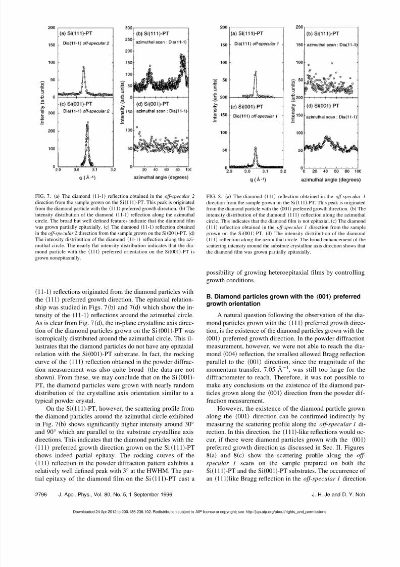
The epitaxial relationship of the diamond particle grownwith the 111 preferred growth direction can be investigatedby studying the associated 11-1 reflection in the off -specular 2 direction. Figures 7a and 7c show the scatter-ing profiles along the off -specular 2 direction that exhibit the
FIG. 6. The rocking curves of the -SiC Bragg reflection from the sampleprepared on a Si111-PT, b Si111-NT, c Si001-PT, and d Si001-NT. The well defined peaks showed that the -SiC films were single crys-tals.
2795J. Appl. Phys., Vol. 80, No. 5, 1 September 1996 J. H. Je and D. Y. Noh
Downloaded 24 Apr 2012 to 200.136.236.102. Redistribution subject to AIP license or copyright; see http://jap.aip.org/about/rights_and_permissions
8/2/2019 Micro Structure of Diamond and SiC Inter Layer Studied by Synchrontron Xray Scattering
11-1 reflections originated from the diamond particles with
the 111 preferred growth direction. The epitaxial relation-ship was studied in Figs. 7b and 7d which show the in-tensity of the 11-1 reflections around the azimuthal circle.As is clear from Fig. 7d, the in-plane crystalline axis direc-tion of the diamond particles grown on the Si001-PT wasisotropically distributed around the azimuthal circle. This il-lustrates that the diamond particles do not have any epitaxialrelation with the Si001-PT substrate. In fact, the rockingcurve of the 111 reflection obtained in the powder diffrac-tion measurement was also quite broad the data are notshown. From these, we may conclude that on the Si001-PT, the diamond particles were grown with nearly randomdistribution of the crystalline axis orientation similar to atypical powder crystal.
On the Si111-PT, however, the scattering profile fromthe diamond particles around the azimuthal circle exhibitedin Fig. 7b shows significantly higher intensity around 30°and 90° which are parallel to the substrate crystalline axisdirections. This indicates that the diamond particles with the111 preferred growth direction grown on the Si111-PTshows indeed partial epitaxy. The rocking curves of the111 reflection in the powder diffraction pattern exhibits arelatively well defined peak with 3° at the HWHM. The par-tial epitaxy of the diamond film on the Si111-PT cast a
possibility of growing heteroepitaxial films by controllinggrowth conditions.
B. Diamond particles grown with the Š001‹ preferredgrowth orientation
A natural question following the observation of the dia-mond particles grown with the 111 preferred growth direc-tion, is the existence of the diamond particles grown with the001 preferred growth direction. In the powder diffractionmeasurement, however, we were not able to reach the dia-mond 004 reflection, the smallest allowed Bragg reflectionparallel to the 001 direction, since the magnitude of themomentum transfer, 7.05 Å1, was still too large for thediffractometer to reach. Therefore, it was not possible tomake any conclusions on the existence of the diamond par-ticles grown along the 001 direction from the powder dif-fraction measurement.
However, the existence of the diamond particle grownalong the 001 direction can be confirmed indirectly bymeasuring the scattering profile along the off -specular 1 di-rection. In this direction, the 111-like reflections would oc-cur, if there were diamond particles grown with the 001
preferred growth direction as discussed in Sec. II. Figures8a and 8c show the scattering profile along the off -specular 1 scans on the sample prepared on both theSi111-PT and the Si001-PT substrates. The occurrence of an 111like Bragg reflection in the off -specular 1 direction
FIG. 7. a The diamond 11-1 reflection obtained in the off -specular 2direction from the sample grown on the Si111-PT. This peak is originatedfrom the diamond particle with the 111 preferred growth direction. b Theintensity distribution of the diamond 11-1 reflection along the azimuthalcircle. The broad but well defined features indicate that the diamond filmwas grown partially epitaxially. c The diamond 11-1 reflection obtainedin the off -specular 2 direction from the sample grown on the Si001-PT. dThe intensity distribution of the diamond 11-1 reflection along the azi-muthal circle. The nearly flat intensity distribution indicates that the dia-mond particle with the 111 preferred orientation on the Si001-PT isgrown nonepitaxially.
FIG. 8. a The diamond 111 reflection obtained in the off -specular 1direction from the sample grown on the Si111-PT. This peak is originatedfrom the diamond particle with the 001 preferred growth direction. b Theintensity distribution of the diamond 111 reflection along the azimuthalcircle. This indicates that the diamond film is not epitaxial. c The diamond111 reflection obtained in the off -specular 1 direction from the samplegrown on the Si001-PT. d The intensity distribution of the diamond111 reflection along the azimuthal circle. The broad enhancement of thescattering intensity around the substrate crystalline axis direction shows thatthe diamond film was grown partially epitaxially.
2796 J. Appl. Phys., Vol. 80, No. 5, 1 September 1996 J. H. Je and D. Y. Noh
Downloaded 24 Apr 2012 to 200.136.236.102. Redistribution subject to AIP license or copyright; see http://jap.aip.org/about/rights_and_permissions
8/2/2019 Micro Structure of Diamond and SiC Inter Layer Studied by Synchrontron Xray Scattering
indicates that there are diamond particles grown with the001 crystalline axis direction aligned to the surface normaldirection. We conclude that there are also diamond particleswith the 001 preferred growth orientation on both theSi111-PT and the Si001-PT.
The diamond particles with the 001 preferred growthdirection show little epitaxial relationship with the sub-strates. Figure 8b shows the diffraction profile along theazimuthal circles originated from the diamond particles withthe 001 preferred orientation on the Si111-PT. The almost
constant intensity distribution indicates that in-plane crystal-line axis direction was nearly isotropically distributed. Therocking curves at the 111 reflection on the off -specular 1
direction have HWHM of about 15°. This shows that thediamond particles are grown preferably along the 001 di-rection although they were not epitaxial. On the Si001-PT,however, the intensity distribution on the azimuthal scan wasbroadly peaked up a shown in Fig. 8d. This indicates thatthe diamond particles grown with the 001 preferred growthdirection on the Si001-PT show partial epitaxy similar tothose with the 111 preferred growth direction on theSi111-PT. We conclude that only the diamond particlesthat were grown with the preferred growth direction match-ing to the substrate normal crystalline axis direction exhibitpartial epitaxy.
V. CONCLUSIONS
In this study, we found that during the MPCVD growthprocess of diamond, the -SiC was always formed asan interlayer. It was always epitaxial to the substrates regard-less of the pretreatment and the orientation of the substrates.The pretreatment of the substrate enhanced the nucleationof the -SiC interlayer significantly specially for theSi111 substrates. On the Si111 substrate, the -SiC inter-
layer was formed with the 111 preferred growth direction,and the orientational relationship can be summarized as -SiC111Si111, and -SiC11-1 Si11-1. Meanwhileon the Si001 substrate, the -SiC interlayer was formedwith the 001 preferred growth direction. On the Si001
substrates, the -SiC 001 direction was parallel to Si001
direction, and the -SiC 111 direction was parallel to theSi111 direction. It was also shown that there were a largeamount of misfit dislocations at the interface between -SiCand Si, resulting from the possible accommodation of thelarge lattice mismatch between -SiC and Si.
Both the diamond particles with the 111 preferredgrowth direction and with the 001 preferred growth direc-tion were grown regardless to the substrate orientation. Onlythe diamond grains that have the preferred growth directionmatching to the substrate normal crystalline axis directionshow partial epitaxial relationship with the substrate. Otherdiamond grains were grown nonepitaxially as indicated bythe constant intensity profile in the azimuthal scans. Thegrowth of diamond particles was also enhanced by the pre-treatment of the substrate. The scattering intensity from thediamond particles on the nontreated substrates was not de-tectable, which indicates the diamond nucleation on the non-treated substrates was minimal. Our study suggests that it is
feasible to grow heteroepitaxial diamond films on pretreatedsilicon substrates, specially on the 111 substrates.
ACKNOWLEDGMENTS
We gratefully acknowledge K. S. Liang and Y. Hwu fortheir valuable discussions. We also express our thank to Z.Fu for his contribution in the synchrotron measurements, andto Y. S. Yang for his efforts in the preparation of thediamond/Si samples. The author also acknowledges the sup-
port from KOSEF95-0300-11-01-3, and D. Y. Noh ac-knowledges the support from K-JISTE60213.
1 S. Matsumoto, Y. Sato, M. Kamo, and N. Setaka, Jpn. J. Appl. Phys. 21,L183 1982.
2 M. Kamo, Y. Sato, S. Matsumoto, and N. Setaka, J. Cryst. Growth 62, 6421983.
3 S. Matsumoto, J. Mater. Sci. Lett. 4, 600 1985.4 A. Sawabe and T. Inuzuka, Appl. Phys. Lett. 46, 146 1985.5 K. Suzuki, A. Sawabe, H. Yasuda, and T. Inuzuka, Appl. Phys. Lett. 50,
728 1987.6 B. R. Stoner, S. R. Sahaida, J. P. Bade, P. Southworth, and P. J. Ellis, J.
Mater. Res. 8, 1334 1993.7 Q. Chen, J. Yang, and Z. Lin, Appl. Phys. Lett. 67, 1853 1995.8 J. E. Field, in The Properties of Diamond , edited by J. E. Field Academic,
London, 1979, p. 284.9 B. E. Williams and J. T. Glass, J. Mater. Res. 4, 373 1989.
10 J. Narayan, A. R. Srivatsa, M. Peters, S. Yokota, and K. V. Ravi, Appl.Phys. Lett. 53, 1823 1988.
11 D. G. Jeng, H. S. Tuan, R. F. Salat, and G. J. Fricano, Appl. Phys. Lett.56, 1968 1990.
12 Y. Sato, I. Yashima, H. Fujita, T. Ando, and M. Kamo, in Proceedings of
the Second International Conference on New Diamond Science and Tech-
nology, edited by R. Messier, J. T. Glass, J. E. Butler, and R. Roy, MRSInternational Conference Proceedings Materials Research Society, Pitts-burgh, 1991, p. 371.
13 W. Zhu, X. H. Wang, B. R. Stoner, G. H. M. Ma, H. S. Kong, M. W. H.Braun, and J. T. Glass, Phys. Rev. B 47, 6529 1993.
14 B. R. Stoner, G.-H. Ma, S. D. Wolter, and J. T. Glass, Phys. Rev. B 45,11 067 1992.
15 B. E. Williams, J. T. Glass, and R. F. Davis, J. Cryst. Growth 99, 11681990.
16 H. C. Shih, C. P. Sung, Y. S. Tang, and J. G. Chen, Surf. Coat. Technol.52, 105 1992.
17 C. P. Sung and H. C. Shih, J. Mater. Res. 7, 105 1992.18 J. H. Je and G. Y. Lee, J. Mater. Sci. 27, 6324 1992.19 W. R. Busing and H. A. Levy, Acta Crystallogr. 22, 457 1967.20 M. Ihara, H. Komiyama, and T. Okubo, Appl. Phys. Lett. 65, 1192 1994.21 C.-P. Chang, D. L. Flamm, D. E. Ibbotson, and J. A. Mucha, J. Appl.
Phys. 63, 744 1988.22 S. Iijima, Y. Aikawa, and K. Baba, J. Mater. Res. 6, 1491 1991.23 K. Hirabayashi, Y. Taniguchi, O. Takamatsu, T. Ikeda, K. Ikoma, and N.
I. Kurihara, Appl. Phys. Lett. 53, 1815 1988.24 S. Yugo, T. Kimura, and H. Kanai, in Science and Technology of New
Diamond , edited by S. Saito, O. Fukunaga, and M. Yoshikawa TerraScientific, Tokyo, 1990, p. 119.
25 S. J. Lin, S. L. Lee, J. Hwang, C. S. Chang, and H. Y. Wen, Appl. Phys.
Lett. 60, 1559 1992.26 A. R. Kirkpatrick, B. W. Ward, and N. P. Economou, J. Vac. Sci. Technol.
B 7, 1947 1989.27 C. R. Lee, J. Y. Leem, and B. S. Chun, J. Mater. Sci. Lett. 14, 361 1995.28 P. A. Denning, H. Shiomi, D. A. Stevenson, and N. M. Johnson, Thin
Solid Films 212, 63 1992.29 R. Ramesham and C. Ellis, J. Mater. Res. 7, 1189 1992.30 B. E. Warren, X -ray Diffraction Addison-Wesley, Reading, MA, 1969,
Chap. 13.31 R. W. Collins, Y. Cong, Y. T. Kim, K. Vedam, Y. Liou, A. Inspektor, and
R. Messier, Thin Solid Films 181, 565 1989.32 R. Meilunas, M. S. Wong, K. C. Sheng, R. P. H. Chang, and R. P. V.
Duyne, Appl. Phys. Lett. 54, 2204 1989.33 H. J. Kim and R. F. Davis, J. Electrochem. Soc. 134, 2269 1987.
2797J. Appl. Phys., Vol. 80, No. 5, 1 September 1996 J. H. Je and D. Y. Noh
Downloaded 24 Apr 2012 to 200.136.236.102. Redistribution subject to AIP license or copyright; see http://jap.aip.org/about/rights_and_permissions
8/2/2019 Micro Structure of Diamond and SiC Inter Layer Studied by Synchrontron Xray Scattering