34
R MicroBlaze and Multimedia Development Board User Guide UG020 (v1.0) August 29, 2002 Product Obsolete/Under Obsolescence

R
MicroBlaze and Multimedia Development BoardUser GuideUG020 (v1.0) August 29, 2002
Product Obsolete/Under Obsolescence

ii www.xilinx.com UG020 (v1.0) August 29, 20021-800-255-7778
"Xilinx" and the Xilinx logo shown above are registered trademarks of Xilinx, Inc. Any rights not expressly granted herein are reserved.
CoolRunner, RocketChips, Rocket IP, Spartan, StateBENCH, StateCAD, Virtex, XACT, XC2064, XC3090, XC4005, and XC5210 are registered trademarks of Xilinx, Inc.
The shadow X shown above is a trademark of Xilinx, Inc.
ACE Controller, ACE Flash, A.K.A. Speed, Alliance Series, AllianceCORE, Bencher, ChipScope, Configurable Logic Cell, CORE Generator, CoreLINX, Dual Block, EZTag, Fast CLK, Fast CONNECT, Fast FLASH, FastMap, Fast Zero Power, Foundation, Gigabit Speeds...and Beyond!, HardWire, HDL Bencher, IRL, J Drive, JBits, LCA, LogiBLOX, Logic Cell, LogiCORE, LogicProfessor, MicroBlaze, MicroVia, MultiLINX, NanoBlaze, PicoBlaze, PLUSASM, PowerGuide, PowerMaze, QPro, Real-PCI, Rocket I/O, SelectI/O, SelectRAM, SelectRAM+, Silicon Xpresso, Smartguide, Smart-IP, SmartSearch, SMARTswitch, System ACE, Testbench In A Minute, TrueMap, UIM, VectorMaze, VersaBlock, VersaRing, Virtex-II Pro, Virtex-II EasyPath, Wave Table, WebFITTER, WebPACK, WebPOWERED, XABEL, XACT-Floorplanner, XACT-Performance, XACTstep Advanced, XACTstep Foundry, XAM, XAPP, X-BLOX +, XC designated products, XChecker, XDM, XEPLD, Xilinx Foundation Series, Xilinx XDTV, Xinfo, XSI, XtremeDSP and ZERO+ are trademarks of Xilinx, Inc.
The Programmable Logic Company is a service mark of Xilinx, Inc.
All other trademarks are the property of their respective owners.
Xilinx, Inc. does not assume any liability arising out of the application or use of any product described or shown herein; nor does it convey any license under its patents, copyrights, or maskwork rights or any rights of others. Xilinx, Inc. reserves the right to make changes, at any time, in order to improve reliability, function or design and to supply the best product possible. Xilinx, Inc. will not assume responsibility for the use of any circuitry described herein other than circuitry entirely embodied in its products. Xilinx provides any design, code, or information shown or described herein "as is." By providing the design, code, or information as one possible implementation of a feature, application, or standard, Xilinx makes no representation that such implementation is free from any claims of infringement. You are responsible for obtaining any rights you may require for your implementation. Xilinx expressly disclaims any warranty whatsoever with respect to the adequacy of any such implementation, including but not limited to any warranties or representations that the implementation is free from claims of infringement, as well as any implied warranties of merchantability or fitness for a particular purpose. Xilinx, Inc. devices and products are protected under U.S. Patents. Other U.S. and foreign patents pending. Xilinx, Inc. does not represent that devices shown or products described herein are free from patent infringement or from any other third party right. Xilinx, Inc. assumes no obligation to correct any errors contained herein or to advise any user of this text of any correction if such be made. Xilinx, Inc. will not assume any liability for the accuracy or correctness of any engineering or software support or assistance provided to a user.
Xilinx products are not intended for use in life support appliances, devices, or systems. Use of a Xilinx product in such applications without the written consent of the appropriate Xilinx officer is prohibited.
The contents of this manual are owned and copyrighted by Xilinx. Copyright 1994-2002 Xilinx, Inc. All Rights Reserved. Except as stated herein, none of the material may be copied, reproduced, distributed, republished, downloaded, displayed, posted, or transmitted in any form or by any means including, but not limited to, electronic, mechanical, photocopying, recording, or otherwise, without the prior written consent of Xilinx. Any unauthorized use of any material contained in this manual may violate copyright laws, trademark laws, the laws of privacy and publicity, and communications regulations and statutes.
MicroBlaze and Multimedia Development Board User Guide UG020 (v1.0) August 29, 2002
The following table shows the revision history for this document..
Version Revision
08/29/02 1.0 Initial Xilinx release.
R
Product Obsolete/Under Obsolescence

UG020 (1.0) August 29, 2002 www.xilinx.com iii1-800-255-7778
MicroBlaze and Multimedia Development Board User GuideSummary ................................................................................................................................ 5PCB Overview ..................................................................................................................... 5
Power Supplies ................................................................................................................. 6TV Input............................................................................................................................. 6TV Output ......................................................................................................................... 7SVGA Output.................................................................................................................... 8Audio Processing ............................................................................................................. 9Ethernet............................................................................................................................ 10RS-232 Port ...................................................................................................................... 11ZBT Memory ................................................................................................................... 12Encryption Support........................................................................................................ 13
FPGA Configuration....................................................................................................... 13CPLD Functions ................................................................................................................ 15
User Input and Output.................................................................................................. 16
Clock Generation ............................................................................................................. 17FPGA User Signal Pinout and Description .......................................................... 19
Reference Design Files .................................................................................................. 34
Contents
Product Obsolete/Under Obsolescence

iv www.xilinx.com UG020 (1.0) August 29, 20021-800-255-7778
R
Product Obsolete/Under Obsolescence

UG020 (1.0) August 29, 2002 www.xilinx.com 51-800-255-7778
R
Chapter 1
MicroBlaze and Multimedia Development Board User Guide
SummaryThe MicroBlaze and Multimedia Development Board is designed to be used as a compact platform for developing multimedia applications. The board supports PAL and NTSC television input and output, true color SVGA output, and an audio CODEC with power amplifier, as well as Ethernet and RS-232 interfaces. Several push button and DIP switches are available for user interaction with the system. The embedded SystemACE™ controller allows for high-speed FPGA configuration from CompactFlash™ storage devices.
PCB Overview Figure 1-1 shows the MicroBlaze and Multimedia Development Board components.
Figure 1-1: MicroBlaze and Multimedia Development Board
ug020_02_060402
Product Obsolete/Under Obsolescence

6 www.xilinx.com UG020 (1.0) August 29, 20021-800-255-7778
Chapter 1: MicroBlaze and Multimedia Development Board User GuideR
Power SuppliesMain power for the board is obtained from an external 5V regulated power supply, which is equipped with an IEC AC input connector for use worldwide with a locally obtained AC line cord.
Local-switch-mode power supplies generate the board’s two main power rails. These power supplies are capable of providing 6 A continuous load current at 3.3 V for ZBT memories and FPGA VCCO, and at 1.5 V for the FPGA VCCINT. If an over-current condition exists, the power supplies automatically shut down. The SystemACE controller FPGA is powered separately by a low-dropout linear regulator, deriving 3.3 V from the external 5 V supply. Isolation of the SystemACE controller FPGA power leaves the full 6 A from the switch-mode power supply available to the user application.
Power for the analog circuitry is created by filtering the main 5 V supply, and the –5 V rail is obtained from an isolated output surface mounted DC-DC converter.
LEDs (shown in Figure 1-2) are used to indicate the status of the primary power supplies. If the voltage output is within ± 10% of the required voltage, the LED is illuminated.
TV InputThe MicroBlaze and Multimedia Development Board supports a single channel of real time video input from a PAL or NTSC source in either composite or S-video (Y/C) format. An Analog Devices ADV7185 video decoder is used to convert standard analog baseband television signals into 4:2:2 component video data compatible with CCIR601/CCIR656 standards. This device utilizes 10 bit A/D converters for broadcast quality digitalization. The decoder creates two line locked clocks that are used to clock the YCrCb data into the FPGA. The first clock, chan1_line_lock_clock1, operates at the sample rate of 27 MHz. The second clock, chan1_line_lock_clock2, operates at the pixel rate of 13.5 MHz. Both of these clocks are routed to FPGA clock pins and IBUFG primitives should instantiated in the design for proper internal clock distribution.
Figure 1-2: Power Supply LEDs
Product Obsolete/Under Obsolescence

UG020 (1.0) August 29, 2002 www.xilinx.com 71-800-255-7778
Chapter 1: MicroBlaze and Multimedia Development Board User GuideR
The operation mode of the decoder is set up over a two wire serial bi-directional port that is I2C compatible. The user selects the video source and type with DIP switches (shown in Figure 1-3), and the I2C controller in the FPGA updates the appropriate registers within the video decoder. A default I2C register setup design has been provided.
The video input to the board is applied to connectors J1 and J19 (highlighted in Figure 1-4). J1 is used for a composite video signal and J19 is used for S-video (Y/C) signals. J1 also carries the left and right line level audio inputs. The barrel color of J1 identifies the specific signal, yellow is the composite video, red is the line level audio right channel and the white is the line level left channel.
TV OutputThe board supports a single channel of real time PAL or NTSC video output. The composite, S-video (Y/C) and RGB formats are all active at the same time. The composite and S-video outputs can be used to drive a television directly, while the RGB outputs can be used to drive a computer monitor or a video projector. Synch information is encoded on each of the RGB outputs.
An Analog Devices ADV7194 video encoder is used to convert the 4:2:2 YCrCb data into broadcast quality base band television signals. The choice of PAL or NTSC output is based
Figure 1-3: Video Source and Mode Selection DIP Switch
Figure 1-4: TV Input Audio/Video Connector
Product Obsolete/Under Obsolescence

8 www.xilinx.com UG020 (1.0) August 29, 20021-800-255-7778
Chapter 1: MicroBlaze and Multimedia Development Board User GuideR
on a signal from the FPGA. The operation mode of the encoder is set up over a two wire serial bi-directional port that is I2C compatible. A default I2C register setup design is provided.
The user has the choice of including timing information in the YCrCb data stream or driving the synch and blanking inputs from the FPGA. This choice is indicated by setting a bit in a specific I2C register.
The video output is turned off until the FPGA enables the output by driving the tv_out_blankz signal High, overriding the pull-down resistor.
It should be noted that if the TV output is enabled, the SVGA output cannot be used, because the YCrCb data bus is shared with the RGB data bus for the SVGA DAC.
The video output from the board is obtained from connectors J2 and J18, as well as the BNC jacks J3-5. J2 is used for a composite video signal and J18 is used for S-video (Y/C) signals and J3-5 provide the red, green, and blue (RGB) outputs. The barrel color of J2 identifies the specific signal, yellow is the composite video, red is the line level audio right channel and the white is the line level left channel. See Figure 1-5.
SVGA OutputIn addition to TV output, the board allows for SVGA output (shown in Figure 1-6). A triple 8-bit DAC with a maximum pixel clock rate of 100 MHz supports a true color SVGA display of 1024 x 768 pixels with a vertical refresh rate of 85 Hz. If a 1024 x 768 bit-mapped display is required, two banks of ZBT RAM must be allocated to video memory; otherwise, a single bank of ZBT RAM allows for a 800 x 600 bit-mapped display. If a character-mode-only display is required, then Virtex-II block RAM can be used as video memory, allowing the ZBT RAMs to be used for other data.
Figure 1-5: TV Output Audio/Video Connectors
Product Obsolete/Under Obsolescence

UG020 (1.0) August 29, 2002 www.xilinx.com 91-800-255-7778
Chapter 1: MicroBlaze and Multimedia Development Board User GuideR
The video DAC provides composite synch on green, for analog monitors that do not have individual horizontal or vertical synch inputs.
It should be noted that if the SVGA output is enabled, the TV output cannot be used, because the YCrCb data bus is shared with the RGB data bus for the SVGA DAC.
The video output is turned off until the FPGA enables the output by driving the vga_out_blankz signal High, overriding the pull-down resistor.
Reference designs are available for both character-mode and bit-mapped SVGA output.
Audio ProcessingThe board includes an audio CODEC that is compliant with AC97, the specification for PC audio. The National Semiconductor LM4549 uses 18-bit Sigma-Delta A/Ds and D/As providing 90 dB of dynamic range. The implementation on this board (shown in Figure 1-7) allows for full duplex stereo A/D and D/A, with one stereo input and two mono inputs, each of which has separate gain, attenuation, and mute control. The mono inputs include a microphone input with 2.2 V bias and a beep tone input from the FPGA. The beep tone input (TTL level) is applied to both outputs, even if the CODEC is held in reset to allow test tones to be heard. The CODEC has two stereo line level outputs with independent volume controls. One of the line level outputs drives the audio output connector and the second line level output drives the on-board power amplifier.
The audio power amplifier is capable of producing 2 W into 8 Ω, in either a bridged mode for driving speakers, or a single-ended mode for driving headphones. When a set of headphones is plugged into the system, the bridged amplifier is disabled and the headphone function is enabled. A volume control is included to adjust the level of both the speaker and headphone output independent of the volume control setting in the CODEC.
The FPGA contains an AC97 Controller that provides control information and PCM data on the outbound link and receives status information and PCM data on the inbound link. The complete AC97 interface consists of four signals:
• The bit_clock (provided by the CODEC)
• A synch pulse generated by the AC97 controller• Two serial data links
The clock signal is routed to an FPGA clock input. An IBUFG primitive should be instantiated in the design for proper internal clock distribution.
The CODEC is held in a reset state until the startup signal is driven High by the FPGA overriding a pull-down resistor.
Figure 1-6: SVGA Video Output Connector
Product Obsolete/Under Obsolescence

10 www.xilinx.com UG020 (1.0) August 29, 20021-800-255-7778
Chapter 1: MicroBlaze and Multimedia Development Board User GuideR
EthernetAn onboard network connection (shown in Figure 1-8) supporting 10/100 Ethernet is also provided. The physical interface is created using a LevelOne LXT972 3.3 Volt PHY. The LXT972 is an IEEE-compliant Fast Ethernet transceiver that directly supports both 100BASE-TX and 10BASE-T applications. It provides a Media Independent Interface (MII) for attachment to the Media Access Controller (MAC) implemented in the FPGA. The device is set up for auto-negotiation of 10/100, full or half duplex operation. Three LED drivers display link status, speed, and receive data.
Each board contains a unique 48-bit serial number that can be used as the MAC address for the board. This serial number is contained in a Dallas Semiconductor “1-Wire” Silicon Serial Number DS2401. A reference design is provided to allow the user to obtain the unique serial number from the one wire serial bus.
The Ethernet PHY is held in a reset state until the startup signal is driven High by the FPGA overriding the pull-down resistor.
The transmit and receive clocks are both generated by the PHY and routed to the FPGA on clock input pins. IBUFG primitives should instantiated in the design for proper internal clock distribution. The Fast Ethernet PHY requires a 25 MHz reference clock input. A dedicated crystal supplies this reference clock.
Figure 1-7: Microphone, Headphone and Speaker Connections
Product Obsolete/Under Obsolescence

UG020 (1.0) August 29, 2002 www.xilinx.com 111-800-255-7778
Chapter 1: MicroBlaze and Multimedia Development Board User GuideR
RS-232 PortIn addition to the Ethernet connection, an RS232 port (pinout identified in Table 1-1) and two PS2 ports are provided (shown in Figure 1-9). These serial ports share connections to the FPGA, all three ports are not available at the same time. The "Serial Port Selection" switches (shown in Figure 1-10) determine the active port(s). The choices are: RS232 TX/RX with CTS/RTS/CSR handshaking, or RS232 data TX/RX only and the PS2 keyboard port, or PS2 keyboard and mouse ports.
Figure 1-8: Ethernet Connector and Status LEDs
Table 1-1: 9-Pin DSUB Connector Pinout
Pin Directions Functions
2 Output Transmitted data
3 Input Received data
5 Ground
6 Output Data set ready
7 Input Request to send
8 Output Clear to send
Product Obsolete/Under Obsolescence

12 www.xilinx.com UG020 (1.0) August 29, 20021-800-255-7778
Chapter 1: MicroBlaze and Multimedia Development Board User GuideR
ZBT MemoryThe board contains five fully-independent banks of 512k x 32 ZBT RAM with a maximum clock rate of 130 MHz. These memories can be used as video frame buffers, SVGA bitmap memory, or general-purpose user RAM. The memory devices support a 36-bit data bus, but pinout limitations on the FPGA prevented the use of the four “parity” bits. The control signals, address and data busses and clock are unique to each bank with no signals shared between the banks. The byte write capability is fully supported. The memory control signals are not equipped with external pull-up resistors. If all five banks of ZBT RAM are not used then configuration options should specify that unused pins have internal pull-up resistors enabled.
Figure 1-9: RS-232 Port Connection
Figure 1-10: Serial-Port Selection Switches
Product Obsolete/Under Obsolescence

UG020 (1.0) August 29, 2002 www.xilinx.com 131-800-255-7778
Chapter 1: MicroBlaze and Multimedia Development Board User GuideR
The clocks for the five banks are all identical in length, and there is a special clock feedback loop that is used to align the clocks at the device pins with a clock internal to the FPGA. More details on clocking are provided in the Clock Generation section.
Sleep mode has been disabled and the burst sequence is set to linear. If the adv_ldz signal is Low, the RAM is accessed based on the externally applied address. If the adv_ldz signal is High, the burst sequence starts with the externally applied address.
A reference design for a ZBR controller driving each bank of memory is provided.
Encryption SupportTo support encryption of configuration data, a battery holder is provided for backing up decryption keys. For this feature to be operational, a CR2032 button cell must be installed.
FPGA ConfigurationThe configuration of the FPGA is controlled by the System Advanced Configuration Environment (SystemACE). The SystemACE environment consists of a controller device (ACE Controller) and a CompactFlash storage device (ACE Flash). The ACE Controller converts the configuration data stored on the CompactFlash into IEEE1149.1 Boundary-Scan (JTAG) serial data. The ACE Controller allows the user to select from one of eight possible configurations each time the board is powered up or the reload push button is pressed. The actual configuration loaded is determined by the “CF CONFIG NUMBER” DIP switch setting as shown in Figure 1-12.
The FPGA can be configured with one of the various download cables, such as the MultiLINX™ or XChecker™ cables. In this case, the download cable should be connected to the JTAG test port header.
Figure 1-11: Battery Holder
Product Obsolete/Under Obsolescence

14 www.xilinx.com UG020 (1.0) August 29, 20021-800-255-7778
Chapter 1: MicroBlaze and Multimedia Development Board User GuideR
The microprocessor interface port on the ACE Controller is connected to the FPGA. This feature allows the user to configure the ACE Controller and have read/write access to the CompactFlash device.
The ACE Controller provides two LEDs as a visual indicator to help monitor device status during operation. See Table 1-2.
Two additional LEDs provide direct indication of the configuration status of the FPGA, even if the ACE Controller has been bypassed through the use of a download cable. The PROG LED indicates that configuration data is being loaded. The DONE LED indicates that configuration data has been successfully loaded. (See Figure 1-13)
Figure 1-12: FPGA Configuration Interface
Table 1-2: ACE Controller Status Indicators
Name Function
ERROR
When ON indicates that an error has occurred
When BLINKING indicates that no CompactFlash device has been detected
When OFF indicates that no errors have been detected
STATUS
When ON indicates the configuration is completed
When BLINKING indicates that configuration is still in progress
When OFF indicates that configuration is in an idle state
Product Obsolete/Under Obsolescence

UG020 (1.0) August 29, 2002 www.xilinx.com 151-800-255-7778
Chapter 1: MicroBlaze and Multimedia Development Board User GuideR
More information on SystemACE is available in DS080, the SystemACE CompactFlash Solution data sheet.
CPLD FunctionsThe CPLD provides housekeeping functions, board control, clock and reset distribution, LED drivers, and push button scanning.
The 27 MHz system clock sets the CPLD clocks, and from this the clocks for the FPGA, SystemACE Controller, and video decoder and encoder are derived. The PCB trace lengths of these signals are all matched to allow the complete system to operate synchronously.
The CPLD also generates reset signals for various system peripherals. Release of these resets is staggered and based on the state of the FPGA, to allow the system to initialize properly. The SystemACE Controller is released from reset approximately 300 ns after the CPLD begins operation and FPGA configuration starts. The video decoder and encoder are held in reset until the FPGA is configured and the fpga_done signal is asserted. These two devices are then configured by the FPGA using the I2C busses.
The audio CODEC and Ethernet PHY are held in reset until the FPGA drives the startup signal High, overriding the pull-down resistor. The startup signal is provided by the FPGA to indicate that the FPGA is ready for the system to become operational. This is especially useful for the audio CODEC, because the beep_tone_in signal is passed directly to the audio amp during reset.
The fpga_done signal is returned to the FPGA as the extend_dcm_reset signal. The clockgen module uses this signal to create an extended reset for the DCMs.
The last function of the CPLD is the scanning of push buttons and the transmission of their status to the FPGA. The FPGA does not have direct access to the push buttons due to pinout limitations. The push buttons are scanned at ~100 Hz. If any change in their status is noted, the red ENTER LED flashes. The push button status is sent to the FPGA only when the ENTER push button is pressed. At this time the associated LED stops flashing, indicating that the data has been transmitted.
A CPLD is programmed from a dedicated JTAG chain connected to the CPLD program header (shown in Figure 1-14).
Figure 1-13: DONE LED Configuration
Product Obsolete/Under Obsolescence

16 www.xilinx.com UG020 (1.0) August 29, 20021-800-255-7778
Chapter 1: MicroBlaze and Multimedia Development Board User GuideR
User Input and OutputTwo different CPLD configuration files are provided. The normal.jed and video.jed files differ in how the push buttons are handled. The push buttons operate in a push-on, push-off mode with no priority in the normal mode. The video mode groups the push buttons into two groups, identified by color. The video source selection push buttons are yellow, and the video effect select buttons are blue. Within each group pressing one of the buttons clears the remaining buttons in the group, so that you cannot select more than one video source or effect. Any change in the push buttons starts the Enter LED flashing until the new data is transmitted in response to a closure of the Enter push button.
Status of push buttons (shown in Figure 1-15) is indicated by associated LEDs. A closed push button is indicated by an illuminated LED and has a logic High transmitted to the FPGA during data transmission.
Push button status information is transmitted to the FPGA serially from the CPLD. The FPGA receives this data and decodes the push button status. Two decoder designs are provided:
• The video_pb_scan_data_in.v design is used with the video.jed CPLD design.
• The pb_scan_data_in.v design is used with the normal.jed CPLD design.
In addition to push button priority encoding, the video_pb_scan_data_in.v design generates two status bits for the second effect push button. This is used for the fade-to and fade-from black effect, where successive data transmissions with the second effect bit set result in the toggling of the fade to and fade from outputs. In addition to the push buttons, two DIP switch inputs connected directly to the FPGA are provided (shown in
Figure 1-14: CPLD Programming Header
Figure 1-15: User Input Push Buttons
Product Obsolete/Under Obsolescence

UG020 (1.0) August 29, 2002 www.xilinx.com 171-800-255-7778
Chapter 1: MicroBlaze and Multimedia Development Board User GuideR
Figure 1-16). The functions of these switches are cdefined by the user. The user is provided two LEDs for use as visual indicators.
Clock GenerationThe internal operation of the FPGA is based on clocks derived from the 27 MHz system clock provided by the CPLD. The master_clock arriving at the FPGA is time aligned with the peripheral clocks. Digital clock managers (DCMs) are used to multiply this clock and to provide internal time alignment, so that the system can operate fully synchronously.
One of the DCMs, the memory_dcm, is used to generate the clock for the ZBT RAMS. This DCM uses a feedback loop that is matched in length to the clock net lengths of the actual memory devices. This allows the memory clocks to synchronize with the memory controllers.
Three internal system clocks and memory clocks are generated: 27 MHz, 53 MHz and 108 MHz. This represents 2, 4, and 8 times the PAL_NTSC pixel rate.
A 50 MHz oscillator drives the alternate_clock input. The pal_ntsc_dcm is used to create a pixel_clock to display PAL or NTSC video on an SVGA monitor.
A DIP switch setting controls a BUFGMUX, which selects between two DCM outputs and determines the specific pixel clock rate.
If a clock that cannot be derived from the 27 MHz or 50 MHz clocks is required, then the 50 MHz oscillator can be replaced.
The extend_dcm_reset input is provided by the CPLD to create a reset pulse for the DCMs after the FPGA has been configured.
Figure 1-17 provides a block diagram of the clock generation module.
Figure 1-16: User Input DIP Switch
Product Obsolete/Under Obsolescence

18w
ww
.xilinx.co
mU
G020 (1.0) A
ugust 29, 20021-800-255-7778
Cha
pter 1:M
icroB
laze and
Mu
ltimed
ia Develo
pm
ent B
oard
User G
uid
eR
Figure 1-17:
Blo
ck Diag
ram o
f the C
lock G
enerato
r Mo
du
le
EXTEND_DCM_RESET_P
MEM_CLK_FBIN_P
MASTER_CLOCK_P
pal_mode
ALTERNATE_CLOCK_P
IBUFG
ALTERNATE_CLOCK
I OCLKFB
CLK0
CLKIN
CLK90
DSSEN
CLK180
PSCLK
CLK270
PSLN
CLK2X
PSINCDEC
CLK2X180
RST
CLKDVCLKFX
CLKFX180LOCKEDPSOONE
STATUS[7:0]PAL_NTSC_DCM
DCM
CLKFB
CLK0
CLKIN
CLK90
DSSEN
CLK180
PSCLK
CLK270
PSLN
CLK2X
PSINCDEC
RST
CLK2X180CLKDVCLKFX
CLKFX180LOCKEDPSOONE
STATUS[7:0]MEMORY_DCM
DCM
MEM_CLK_FBOUT_P
clk_54mhz
memory_27mhz
clk_108mhz
pixel_clock
memory_108mhz
fpga_reset
memory_54mhz
clk_27mhz
OBUF_F_12
MEMORY_FB_OUT
I
I
O
O
CLK54_BUF
BUFG
I O
BUFG
CLK108_BUF
O
BUFGMUXI0I1S
CLKFB
CLK0
CLKIN
CLK90
DSSEN
CLK180
PSCLK
CLK270
PSLN
CLK2X
PSINCDECRST
CLK2X180CLKDVCLKFX
CLKFX180LOCKEDPSOONE
STATUS[7:0]MAIN_DCM
DCM
IBUFI O
DCM_RESET
IBUFGI O
MASTER_CLOCK
IBUFGI O
MEMORY_FB_IN
PIXEL_CLK_MUX
BUFGI O
CLK27_BUF
fpga_reset
in1_fpga_reset
D[15:0] O[15:0]
enable_reset_counter
dcm
reset_counter_4[15:0] n_reset_counter[15:0]
terminal_count 10
ug020_1_17_061402
Product Obsolete/Under Obsolescence

UG020 (1.0) August 29, 2002 www.xilinx.com 191-800-255-7778
Chapter 1: MicroBlaze and Multimedia Development Board User GuideR
FPGA User Signal Pinout and DescriptionTable 1-3: TV Input
Signal Name FPGA Pin Direction Function
CHAN1_VIDEO_DATA0 B15 Input Multiplexed YCrCb pixel port supplying 4:2:2 component video compatible with CCIR656/601 standards.
CHAN1_VIDEO_DATA1 B14 Input
CHAN1_VIDEO_DATA2 D14 Input
CHAN1_VIDEO_DATA3 D15 Input
CHAN1_VIDEO_DATA4 G15 Input
CHAN1_VIDEO_DATA5 H15 Input
CHAN1_VIDEO_DATA6 A14 Input
CHAN1_VIDEO_DATA7 A13 Input
CHAN1_VIDEO_DATA8 E10 Input
CHAN1_VIDEO_DATA9 E11 Input
CHAN1_LINE_LOCK_CLOCK1 C15 GCLK3P
Input Line locked pixel clock (27 MHz)
CHAN1_LINE_LOCK_CLOCK2 C14GCLK2S
Input Line locked clock (13.5 MHz)
CHAN1_ISO D9 Output Input switch over indicated to the video decoder that the input source has changed.
CHAN1_I2C_CLOCK H12 Output I2C port serial interface clock.
CHAN1_I2C_DATA H11 Bi-directional I2C port serial data.
Table 1-4: TV Output
Signal Name FPGA Pin Direction Function
VGA_OUT_GREEN6_YCrCb0 F22 Output Multiplexed YCrCb pixel port supplying 4:2:2 component video compatible with CCIR656/601 standards.
VGA_OUT_GREEN7_YCrCb1 F23 Output
VGA_OUT_BLUE0_YCrCb2 C30 Output
VGA_OUT_BLUE1_YCrCb3 B30 Output
VGA_OUT_BLUE2_YCrCb4 G23 Output
VGA_OUT_BLUE3_YCrCb5 H23 Output
VGA_OUT_BLUE4_YCrCb6 D28 Output
VGA_OUT_BLUE5_YCrCb7 E28 Output
VGA_OUT_BLUE6_YCrCb8 D29 Output
VGA_OUT_BLUE7_YCrCb9 C29 Output
TV_OUT_PAL_NTSCZ G24 Output Selects either PAL or NTSC operation. Logic 0 selects NTSC.
TV_OUT_HSYNCHZ H22 Output Horizontal Synch active Low.
TV_OUT_VSYNCHZ J23 Output Vertical Synch active Low.
TV_OUT_BLANKZ F27 Output Blanks the video encoder output, active Low with pull down resistor
Product Obsolete/Under Obsolescence

20 www.xilinx.com UG020 (1.0) August 29, 20021-800-255-7778
Chapter 1: MicroBlaze and Multimedia Development Board User GuideR
TV_OUT_SUB_CARRIER_RESET D30 Output Color subcarrier reset
VIDEO_ENCODER_SCLK E27 Output I2C port serial interface clock
VIDEO_ENCODER_DATA E30 Bi-directional I2C port serial data
Table 1-4: TV Output (Continued)
Signal Name FPGA Pin Direction Function
Table 1-5: SVGA Output
Signal Name FPGA Pin Direction Function
VGA_OUT_RED0 E23 Output Data bus for the Red DAC.
VGA_OUT_RED1 E22 Output
VGA_OUT_RED2 H20 Output
VGA_OUT_RED3 H21 Output
VGA_OUT_RED4 B24 Output
VGA_OUT_RED5 B23 Output
VGA_OUT_RED6 D23 Output
VGA_OUT_RED7 D24 Output
VGA_OUT_GREEN0 G21 Output Data bus for the Blue DAC.
VGA_OUT_GREEN1 G22 Output
VGA_OUT_GREEN2 B25 Output
VGA_OUT_GREEN3 A24 Output
VGA_OUT_GREEN4 D25 Output
VGA_OUT_GREEN5 C24 Output
VGA_OUT_GREEN6_YCrCb0 F22 Output
VGA_OUT_GREEN7_YCrCb1 F23 Output
VGA_OUT_BLUE0_YCrCb2 C30 Output Data bus for the Green DAC.
VGA_OUT_BLUE1_YCrCb3 B30 Output
VGA_OUT_BLUE2_YCrCb4 G23 Output
VGA_OUT_BLUE3_YCrCb5 H23 Output
VGA_OUT_BLUE4_YCrCb6 D28 Output
VGA_OUT_BLUE5_YCrCb7 E28 Output
VGA_OUT_BLUE6_YCrCb8 D29 Output
VGA_OUT_BLUE7_YCrCb9 C29 Output
VGA_OUT_COMP_SYNCH A26 Output Composite Synch
VGA_OUT_BLANK_Z A25 Output Blanks the DAC output, active Low with pull down resistor.
Product Obsolete/Under Obsolescence

UG020 (1.0) August 29, 2002 www.xilinx.com 211-800-255-7778
Chapter 1: MicroBlaze and Multimedia Development Board User GuideR
VGA_OUT_PIXEL_CLOCK A27 Output Pixel clock for the DAC.
VGA_HSYNCH F24 Output Horizontal Synch for the SVGA monitor.
VGA_VSYNCH E24 Output Vertical Synch for the SVGA monitor.
Table 1-5: SVGA Output (Continued)
Signal Name FPGA Pin Direction Function
Table 1-6: Fast Ethernet
Signal Name FPGA Pin Direction Function
TX_DATA0 G20 Output Transmit data
TX_DATA1 B21 Output
TX_DATA2 B20 Output
TX_DATA3 C22 Output
TX_ENABLE G19 Output Transmit enable
TX_CLOCK H16GCLK7P
Input Transmit clock sourced by the PHY.
TX_ERROR D21 Input Transmit error condition
ENET_SLEW0 G16 Output Slew rate control for the TX output.
ENET_SLEW1 C16 Output
RX_DATA0 B16 Input Receive data
RX_DATA1 F17 Input
RX_DATA2 F16 Input
RX_DATA3 D16 Input
RX_CLOCK C17GCLK5P
Input Receive clock sourced by the PHY.
RX_DATA_VALID B17 Input Receive data valid
RX_ERROR D22 Input Receive error condition
COLLISION_DETECTED C23 Input Collision detected during full duplex operation.
CARRIER_SENSE F20 Input During half duplex operation this is asserted when transmitting or receiving data packets. During full duplex operation this signal is asserted during receive.
PAUSE A16 Output When set High the pause capabilities are advertised during auto-negotiation.
MDIO A17 Bi-directional Management Data Input/Output Serial data channel.
Product Obsolete/Under Obsolescence

22 www.xilinx.com UG020 (1.0) August 29, 20021-800-255-7778
Chapter 1: MicroBlaze and Multimedia Development Board User GuideR
MDC D17 Output Management Data Clock used to clock the MDIO serial data channel.
MDINIT_Z F21 Input Management Data Interrupt active Low indication of a status change.
SSN_DATA A22 Bi-directional One wire interface to the silicon serial number (MAC address).
Table 1-6: Fast Ethernet (Continued)
Signal Name FPGA Pin Direction Function
Table 1-7: RS-232 Port and PS2 Ports
Signal Name FPGA Pin Direction Function
RS232_TX_DATA C9 Output Transmitted data
MOUSE_CLOCK Bidirectional Clock for PS2 mouse
RS232_RX_DATA C8 Input Received data
MOUSE_DATA Bidirectional PS2 mouse data
RS232_CTS_OUT F11 Output Clear to send
KBD_CLOCK Bidirectional Clock for PS2 keyboard
RS232_DSR_OUT F10 Output Data set ready
KBD_DATA Bidirectional PS2 keyboard data
RS232_RTS_IN B8 Input Request to send
Table 1-8: AC97 Audio CODEC
Signal Name FPGA Pin Direction Function
AC97_DATA_IN B9 Input PCM data and status information from the CODEC.
AC97_DATA_OUT E8 Output PCM data and control information to the CODEC.
AC97_BIT_CLOCK F15GCLK1P
Input 12.288 MHz clock from the CODEC. Data is sampled on the falling edge of the clock.
AC97_SYNCH E9 Output 48 kHz synch pulse signifies the start of the serial data streams.
BEEP_TONE_IN G11 Output TTL level tone that is summed to both stereo outputs.
Product Obsolete/Under Obsolescence

UG020 (1.0) August 29, 2002 www.xilinx.com 231-800-255-7778
Chapter 1: MicroBlaze and Multimedia Development Board User GuideR
Table 1-9: User Input and Output
Signal Name FPGA Pin Direction Function
USER_INPUT0 D10 Input User defined input with pull-up resistor.
USER_INPUT1 F14 Input User defined input with pull-up resistor.
PB_CLOCK AK6 Input Clock for the serially transmitted push button status.
PB_DATA AG6 Input Serially transmitted push button status.
USER_LED0_Z B27 Output Active Low output to turn on a user defined LED 0.
USER_LED1_Z B22 Output Active Low output to turn on a user defined LED 1.
PAL_NTSC_Z C26 Input Selects either PAL or NTSC video formats. Low selects NTSC.
S_VIDEO_Z C25 Input Selects either S-Video or Composite video source. Low selects S-Video.
Table 1-10: SystemACE Micro Port
Signal Name FPGA Pin Direction Function
MPD0 AE3 Bi-directional Micro Port data bus.
MPD1 AD6 Bi-directional
MPD2 AD7 Bi-directional
MPD3 AF1 Bi-directional
MPD4 AG1 Bi-directional
MPD5 AD4 Bi-directional
MPD6 AE4 Bi-directional
MPD7 AD8 Bi-directional
MPD8 AE7 Bi-directional
MPD9 AG2 Bi-directional
MPD10 AH2 Bi-directional
MPD11 AD5 Bi-directional
MPD12 AE5 Bi-directional
MPD13 AC9 Bi-directional
MPD14 AD9 Bi-directional
MPD15 AH1 Bi-directional
MPA0 AJ1 Output Micro Port address bus.
MPA1 AF4 Output
MPA2 AG3 Output
Product Obsolete/Under Obsolescence

24 www.xilinx.com UG020 (1.0) August 29, 20021-800-255-7778
Chapter 1: MicroBlaze and Multimedia Development Board User GuideR
MPA3 AK2 Output
MPA4 AE8 Output
MPA5 AF9 Output
MPA6 AH5 Output
MPCE_Z AH6 Output Micro Port chip enable active Low with pull-up internal to the SystemACE controller.
MPWE_Z AJ4 Output Micro Port write enable active Low with pull-up internal to the SystemACE controller.
MPOE_Z AK4 Output Micro Port output enable active Low with pull-up internal to the SystemACE controller.
MPIRQ AC10 Input Micro Port Interrupt Request flag.
MPBRDY AC11 Input Micro Port data Buffer Ready flag.
Table 1-10: SystemACE Micro Port (Continued)
Signal Name FPGA Pin Direction Function
Table 1-11: ZBT RAM BANK0
Signal Name FPGA Pin Direction Function
MEMORY_BANK0_ADDR0 T23 Output Address bus.
MEMORY_BANK0_ADDR1 U23 Output
MEMORY_BANK0_ADDR2 AB29 Output
MEMORY_BANK0_ADDR3 AA29 Output
MEMORY_BANK0_ADDR4 AA27 Output
MEMORY_BANK0_ADDR5 AB27 Output
MEMORY_BANK0_ADDR6 H25 Output
MEMORY_BANK0_ADDR7 G25 Output
MEMORY_BANK0_ADDR8 G28 Output
MEMORY_BANK0_ADDR9 H29 Output
MEMORY_BANK0_ADDR10 U27 Output
MEMORY_BANK0_ADDR11 T27 Output
MEMORY_BANK0_ADDR12 V29 Output
MEMORY_BANK0_ADDR13 U29 Output
MEMORY_BANK0_ADDR14 T24 Output
MEMORY_BANK0_ADDR15 T25 Output
MEMORY_BANK0_ADDR16 U28 Output
MEMORY_BANK0_ADDR17 F28 Output
MEMORY_BANK0_ADDR18 L23 Output
MEMORY_BANK0_DATA_A0 T30 Bi-directional Data bus for byte-A
Product Obsolete/Under Obsolescence

UG020 (1.0) August 29, 2002 www.xilinx.com 251-800-255-7778
Chapter 1: MicroBlaze and Multimedia Development Board User GuideR
MEMORY_BANK0_DATA_A1 P28 Bi-directional
MEMORY_BANK0_DATA_A2 R25 Bi-directional
MEMORY_BANK0_DATA_A3 R29 Bi-directional
MEMORY_BANK0_DATA_A4 R27 Bi-directional
MEMORY_BANK0_DATA_A5 R23 Bi-directional
MEMORY_BANK0_DATA_A6 N30 Bi-directional
MEMORY_BANK0_DATA_A7 K26 Bi-directional
MEMORY_BANK0_DATA_B0 M25 Bi-directional Data bus for byte-B
MEMORY_BANK0_DATA_B1 J29 Bi-directional
MEMORY_BANK0_DATA_B2 K27 Bi-directional
MEMORY_BANK0_DATA_B3 L24 Bi-directional
MEMORY_BANK0_DATA_B4 H27 Bi-directional
MEMORY_BANK0_DATA_B5 H26 Bi-directional
MEMORY_BANK0_DATA_B6 K25 Bi-directional
MEMORY_BANK0_DATA_B7 H28 Bi-directional
MEMORY_BANK0_DATA_C0 J25 Bi-directional Data bus for byte-C
MEMORY_BANK0_DATA_C1 J26 Bi-directional
MEMORY_BANK0_DATA_C2 J28 Bi-directional
MEMORY_BANK0_DATA_C3 K24 Bi-directional
MEMORY_BANK0_DATA_C4 J27 Bi-directional
MEMORY_BANK0_DATA_C5 K29 Bi-directional
MEMORY_BANK0_DATA_C6 L25 Bi-directional
MEMORY_BANK0_DATA_C7 L26 Bi-directional
MEMORY_BANK0_DATA_D0 P30 Bi-directional Data bus for byte-D
MEMORY_BANK0_DATA_D1 P23 Bi-directional
MEMORY_BANK0_DATA_D2 P27 Bi-directional
MEMORY_BANK0_DATA_D3 T29 Bi-directional
MEMORY_BANK0_DATA_D4 R24 Bi-directional
MEMORY_BANK0_DATA_D5 R28 Bi-directional
MEMORY_BANK0_DATA_D6 U30 Bi-directional
MEMORY_BANK0_DATA_D7 T28 Bi-directional
MEMORY_BANK0_CLK G27 Output
MEMORY_BANK0_CLKEN_Z G30 Output Clock enable active Low
MEMORY_BANK0_WEN_Z F26 Output Write enable active Low
Table 1-11: ZBT RAM BANK0 (Continued)
Signal Name FPGA Pin Direction Function
Product Obsolete/Under Obsolescence

26 www.xilinx.com UG020 (1.0) August 29, 20021-800-255-7778
Chapter 1: MicroBlaze and Multimedia Development Board User GuideR
MEMORY_BANK0_WENA_Z J24 Output Byte-A write control active Low
MEMORY_BANK0_WENB_Z H24 Output Byte-B write control active Low
MEMORY_BANK0_WENC_Z F29 Output Byte-C write control active Low
MEMORY_BANK0_WEND_Z G29 Output Byte-D write control active Low
MEMORY_BANK0_CEN_Z G26 Output Chip enable active Low
MEMORY_BANK0_OEN_Z F30 Output Output enable active Low
MEMORY_BANK0_ADV_LDZ K23 Output Burst operation load starting address when Low or advance to next address when High.
Table 1-11: ZBT RAM BANK0 (Continued)
Signal Name FPGA Pin Direction Function
Table 1-12: ZBT RAM BANK1
Signal Name FPGA Pin Direction Function
MEMORY_BANK1_ADDR0 AG25 Output Address bus.
MEMORY_BANK1_ADDR1 AJ24 Output
MEMORY_BANK1_ADDR2 AJ25 Output
MEMORY_BANK1_ADDR3 AD22 Output
MEMORY_BANK1_ADDR4 AE21 Output
MEMORY_BANK1_ADDR5 AH25 Output
MEMORY_BANK1_ADDR6 W25 Output
MEMORY_BANK1_ADDR7 Y25 Output
MEMORY_BANK1_ADDR8 AB26 Output
MEMORY_BANK1_ADDR9 AC26 Output
MEMORY_BANK1_ADDR10 AG24 Output
MEMORY_BANK1_ADDR11 AC20 Output
MEMORY_BANK1_ADDR12 AC21 Output
MEMORY_BANK1_ADDR13 AK26 Output
MEMORY_BANK1_ADDR14 AK27 Output
MEMORY_BANK1_ADDR15 AH26 Output
MEMORY_BANK1_ADDR16 AJ27 Output
MEMORY_BANK1_ADDR17 AA23 Output
MEMORY_BANK1_ADDR18 Y23 Output
MEMORY_BANK1_DATA_A0 AE23 Bi-directional Data bus for byte-A
MEMORY_BANK1_DATA_A1 AK29 Bi-directional
MEMORY_BANK1_DATA_A2 AB23 Bi-directional
MEMORY_BANK1_DATA_A3 AF28 Bi-directional
Product Obsolete/Under Obsolescence

UG020 (1.0) August 29, 2002 www.xilinx.com 271-800-255-7778
Chapter 1: MicroBlaze and Multimedia Development Board User GuideR
MEMORY_BANK1_DATA_A4 AH30 Bi-directional
MEMORY_BANK1_DATA_A5 AC23 Bi-directional
MEMORY_BANK1_DATA_A6 AE27 Bi-directional
MEMORY_BANK1_DATA_A7 AH29 Bi-directional
MEMORY_BANK1_DATA_B0 AD24 Bi-directional Data bus for byte-B
MEMORY_BANK1_DATA_B1 AD26 Bi-directional
MEMORY_BANK1_DATA_B2 AF30 Bi-directional
MEMORY_BANK1_DATA_B3 AC25 Bi-directional
MEMORY_BANK1_DATA_B4 AD28 Bi-directional
MEMORY_BANK1_DATA_B5 AE29 Bi-directional
MEMORY_BANK1_DATA_B6 AB24 Bi-directional
MEMORY_BANK1_DATA_B7 AC27 Bi-directional
MEMORY_BANK1_DATA_C0 AD27 Bi-directional Data bus for byte-C
MEMORY_BANK1_DATA_C1 AC24 Bi-directional
MEMORY_BANK1_DATA_C2 AD29 Bi-directional
MEMORY_BANK1_DATA_C3 AE28 Bi-directional
MEMORY_BANK1_DATA_C4 AD25 Bi-directional
MEMORY_BANK1_DATA_C5 AG30 Bi-directional
MEMORY_BANK1_DATA_C6 AE26 Bi-directional
MEMORY_BANK1_DATA_C7 AE24 Bi-directional
MEMORY_BANK1_DATA_D0 AG29 Bi-directional Data bus for byte-D
MEMORY_BANK1_DATA_D1 AF27 Bi-directional
MEMORY_BANK1_DATA_D2 AD23 Bi-directional
MEMORY_BANK1_DATA_D3 AJ30 Bi-directional
MEMORY_BANK1_DATA_D4 AG28 Bi-directional
MEMORY_BANK1_DATA_D5 AC22 Bi-directional
MEMORY_BANK1_DATA_D6 AJ28 Bi-directional
MEMORY_BANK1_DATA_D7 AE22 Bi-directional
MEMORY_BANK1_CLK AB25 Output
MEMORY_BANK1_CLKEN_Z AD30 Output Clock enable active Low
MEMORY_BANK1_WEN_Z AE30 Output Write enable active Low
MEMORY_BANK1_WENA_Z AA25 Output Byte-A write control active Low
MEMORY_BANK1_WENB_Z AA24 Output Byte-B write control active Low
MEMORY_BANK1_WENC_Z Y24 Output Byte-C write control active Low
Table 1-12: ZBT RAM BANK1 (Continued)
Signal Name FPGA Pin Direction Function
Product Obsolete/Under Obsolescence

28 www.xilinx.com UG020 (1.0) August 29, 20021-800-255-7778
Chapter 1: MicroBlaze and Multimedia Development Board User GuideR
MEMORY_BANK1_WEND_Z AC29 Output Byte-D write control active Low
MEMORY_BANK1_CEN_Z AB30 Output Chip enable active Low
MEMORY_BANK1_OEN_Z AB28 Output Output enable active Low
MEMORY_BANK1_ADV_LDZ AC28 Output Burst operation load starting address when Low or advance to next address when High.
Table 1-12: ZBT RAM BANK1 (Continued)
Signal Name FPGA Pin Direction Function
Table 1-13: ZBT RAM BANK2
Signal Name FPGA Pin Direction Function
MEMORY_BANK2_ADDR0 AJ6 Output Address bus.
MEMORY_BANK2_ADDR1 AK7 Output
MEMORY_BANK2_ADDR2 AF8 Output
MEMORY_BANK2_ADDR3 AF7 Output
MEMORY_BANK2_ADDR4 AE10 Output
MEMORY_BANK2_ADDR5 AE9 Output
MEMORY_BANK2_ADDR6 AH24 Output
MEMORY_BANK2_ADDR7 AK24 Output
MEMORY_BANK2_ADDR8 AG22 Output
MEMORY_BANK2_ADDR9 AH23 Output
MEMORY_BANK2_ADDR10 AD10 Output
MEMORY_BANK2_ADDR11 AD11 Output
MEMORY_BANK2_ADDR12 AG8 Output
MEMORY_BANK2_ADDR13 AG7 Output
MEMORY_BANK2_ADDR14 AJ8 Output
MEMORY_BANK2_ADDR15 AJ7 Output
MEMORY_BANK2_ADDR16 AE11 Output
MEMORY_BANK2_ADDR17 AG21 Output
MEMORY_BANK2_ADDR18 AF22 Output
MEMORY_BANK2_DATA_A0 AG9 Bi-directional Data bus for byte-A
MEMORY_BANK2_DATA_A1 AK9 Bi-directional
MEMORY_BANK2_DATA_A2 AH8 Bi-directional
MEMORY_BANK2_DATA_A3 AF11 Bi-directional
MEMORY_BANK2_DATA_A4 AJ14 Bi-directional
MEMORY_BANK2_DATA_A5 AC14 Bi-directional
MEMORY_BANK2_DATA_A6 AG15 Bi-directional
Product Obsolete/Under Obsolescence

UG020 (1.0) August 29, 2002 www.xilinx.com 291-800-255-7778
Chapter 1: MicroBlaze and Multimedia Development Board User GuideR
MEMORY_BANK2_DATA_A7 AK14 Bi-directional
MEMORY_BANK2_DATA_B0 AD15 Bi-directional Data bus for byte-B
MEMORY_BANK2_DATA_B1 AH17 Bi-directional
MEMORY_BANK2_DATA_B2 AJ16 Bi-directional
MEMORY_BANK2_DATA_B3 AG17 Bi-directional
MEMORY_BANK2_DATA_B4 AC16 Bi-directional
MEMORY_BANK2_DATA_B5 AK17 Bi-directional
MEMORY_BANK2_DATA_B6 AF21 Bi-directional
MEMORY_BANK2_DATA_B7 AH22 Bi-directional
MEMORY_BANK2_DATA_C0 AF20 Bi-directional Data bus for byte-C
MEMORY_BANK2_DATA_C1 AK18 Bi-directional
MEMORY_BANK2_DATA_C2 AC17 Bi-directional
MEMORY_BANK2_DATA_C3 AG16 Bi-directional
MEMORY_BANK2_DATA_C4 AJ17 Bi-directional
MEMORY_BANK2_DATA_C5 AE16 Bi-directional
MEMORY_BANK2_DATA_C6 AH16 Bi-directional
MEMORY_BANK2_DATA_C7 AK15 Bi-directional
MEMORY_BANK2_DATA_D0 AG14 Bi-directional Data bus for byte-D
MEMORY_BANK2_DATA_D1 AC15 Bi-directional
MEMORY_BANK2_DATA_D2 AJ15 Bi-directional
MEMORY_BANK2_DATA_D3 AF10 Bi-directional
MEMORY_BANK2_DATA_D4 AH9 Bi-directional
MEMORY_BANK2_DATA_D5 AJ9 Bi-directional
MEMORY_BANK2_DATA_D6 AG10 Bi-directional
MEMORY_BANK2_DATA_D7 AE12 Bi-directional
MEMORY_BANK2_CLK AJ22 Output
MEMORY_BANK2_CLKEN_Z AE20 Output Clock enable active Low
MEMORY_BANK2_WEN_Z AJ23 Output Write enable active Low
MEMORY_BANK2_WENA_Z AF24 Output Byte-A write control active Low
MEMORY_BANK2_WENB_Z AG23 Output Byte-B write control active Low
MEMORY_BANK2_WENC_Z AD20 Output Byte-C write control active Low
MEMORY_BANK2_WEND_Z AD21 Output Byte-D write control active Low
Table 1-13: ZBT RAM BANK2 (Continued)
Signal Name FPGA Pin Direction Function
Product Obsolete/Under Obsolescence

30 www.xilinx.com UG020 (1.0) August 29, 20021-800-255-7778
Chapter 1: MicroBlaze and Multimedia Development Board User GuideR
MEMORY_BANK2_CEN_Z AK25 Output Chip enable active Low
MEMORY_BANK2_OEN_Z AE19 Output Output enable active Low
MEMORY_BANK2_ADV_LDZ AF23 Output Burst operation load starting address when Low or advance to next address when High.
Table 1-13: ZBT RAM BANK2 (Continued)
Signal Name FPGA Pin Direction Function
Table 1-14: ZBT RAM BANK3
Signal Name FPGA Pin Direction Function
MEMORY_BANK3_ADDR0 AC5 Output Address bus.
MEMORY_BANK3_ADDR1 AC8 Output
MEMORY_BANK3_ADDR2 AB8 Output
MEMORY_BANK3_ADDR3 AE2 Output
MEMORY_BANK3_ADDR4 AF4 Output
MEMORY_BANK3_ADDR5 AD3 Output
MEMORY_BANK3_ADDR6 J4 Output
MEMORY_BANK3_ADDR7 K4 Output
MEMORY_BANK3_ADDR8 R1 Output
MEMORY_BANK3_ADDR9 T2 Output
MEMORY_BANK3_ADDR10 AB5 Output
MEMORY_BANK3_ADDR11 AC4 Output
MEMORY_BANK3_ADDR12 AB4 Output
MEMORY_BANK3_ADDR13 AC7 Output
MEMORY_BANK3_ADDR14 AB7 Output
MEMORY_BANK3_ADDR15 AC3 Output
MEMORY_BANK3_ADDR16 AB3 Output
MEMORY_BANK3_ADDR17 R4 Output
MEMORY_BANK3_ADDR18 P4 Output
MEMORY_BANK3_DATA_A0 AD1 Bi-directional Data bus for byte-A
MEMORY_BANK3_DATA_A1 AC6 Bi-directional
MEMORY_BANK3_DATA_A2 Y7 Bi-directional
MEMORY_BANK3_DATA_A3 AC2 Bi-directional
MEMORY_BANK3_DATA_A4 Y8 Bi-directional
MEMORY_BANK3_DATA_A5 Y5 Bi-directional
MEMORY_BANK3_DATA_A6 AA2 Bi-directional
MEMORY_BANK3_DATA_A7 AA6 Bi-directional
Product Obsolete/Under Obsolescence

UG020 (1.0) August 29, 2002 www.xilinx.com 311-800-255-7778
Chapter 1: MicroBlaze and Multimedia Development Board User GuideR
MEMORY_BANK3_DATA_B0 T4 Bi-directional Data bus for byte-B
MEMORY_BANK3_DATA_B1 U2 Bi-directional
MEMORY_BANK3_DATA_B2 T8 Bi-directional
MEMORY_BANK3_DATA_B3 T3 Bi-directional
MEMORY_BANK3_DATA_B4 U1 Bi-directional
MEMORY_BANK3_DATA_B5 T7 Bi-directional
MEMORY_BANK3_DATA_B6 R3 Bi-directional
MEMORY_BANK3_DATA_B7 R7 Bi-directional
MEMORY_BANK3_DATA_C0 R6 Bi-directional Data bus for byte-C
MEMORY_BANK3_DATA_C1 P3 Bi-directional
MEMORY_BANK3_DATA_C2 T6 Bi-directional
MEMORY_BANK3_DATA_C3 V1 Bi-directional
MEMORY_BANK3_DATA_C4 U3 Bi-directional
MEMORY_BANK3_DATA_C5 U8 Bi-directional
MEMORY_BANK3_DATA_C6 V2 Bi-directional
MEMORY_BANK3_DATA_C7 U4 Bi-directional
MEMORY_BANK3_DATA_D0 Y6 Bi-directional Data bus for byte-D
MEMORY_BANK3_DATA_D1 AB2 Bi-directional
MEMORY_BANK3_DATA_D2 AA5 Bi-directional
MEMORY_BANK3_DATA_D3 AA8 Bi-directional
MEMORY_BANK3_DATA_D4 AD2 Bi-directional
MEMORY_BANK3_DATA_D5 AA7 Bi-directional
MEMORY_BANK3_DATA_D6 AB6 Bi-directional
MEMORY_BANK3_DATA_D7 AE1 Bi-directional
MEMORY_BANK3_CLK K5 Output
MEMORY_BANK3_CLKEN_Z P2 Output Clock enable active Low
MEMORY_BANK3_WEN_Z R2 Output Write enable active Low
MEMORY_BANK3_WENA_Z L5 Output Byte-A write control active Low
MEMORY_BANK3_WENB_Z M6 Output Byte-B write control active Low
MEMORY_BANK3_WENC_Z L6 Output Byte-C write control active Low
MEMORY_BANK3_WEND_Z J1 Output Byte-D write control active Low
Table 1-14: ZBT RAM BANK3 (Continued)
Signal Name FPGA Pin Direction Function
Product Obsolete/Under Obsolescence

32 www.xilinx.com UG020 (1.0) August 29, 20021-800-255-7778
Chapter 1: MicroBlaze and Multimedia Development Board User GuideR
MEMORY_BANK3_CEN_Z K1 Output Chip enable active Low
MEMORY_BANK3_OEN_Z P8 Output Output enable active Low
MEMORY_BANK3_ADV_LDZ R8 Output Burst operation load starting address when Low or advance to next address when High.
Table 1-14: ZBT RAM BANK3 (Continued)
Signal Name FPGA Pin Direction Function
Table 1-15: ZBT RAM BANK4
Signal Name FPGA Pin Direction Function
MEMORY_BANK4_ADDR0 J5 Output Address bus.
MEMORY_BANK4_ADDR1 H5 Output
MEMORY_BANK4_ADDR2 J3 Output
MEMORY_BANK4_ADDR3 H3 Output
MEMORY_BANK4_ADDR4 K7 Output
MEMORY_BANK4_ADDR5 L7 Output
MEMORY_BANK4_ADDR6 H10 Output
MEMORY_BANK4_ADDR7 B7 Output
MEMORY_BANK4_ADDR8 C5 Output
MEMORY_BANK4_ADDR9 D7 Output
MEMORY_BANK4_ADDR10 K6 Output
MEMORY_BANK4_ADDR11 J6 Output
MEMORY_BANK4_ADDR12 H2 Output
MEMORY_BANK4_ADDR13 J2 Output
MEMORY_BANK4_ADDR14 H4 Output
MEMORY_BANK4_ADDR15 G4 Output
MEMORY_BANK4_ADDR16 L8 Output
MEMORY_BANK4_ADDR17 B6 Output
MEMORY_BANK4_ADDR18 G8 Output
MEMORY_BANK4_DATA_A0 F1 Bi-directional Data bus for byte-A
MEMORY_BANK4_DATA_A1 F3 Bi-directional
MEMORY_BANK4_DATA_A2 J7 Bi-directional
MEMORY_BANK4_DATA_A3 F2 Bi-directional
MEMORY_BANK4_DATA_A4 G5 Bi-directional
MEMORY_BANK4_DATA_A5 H6 Bi-directional
MEMORY_BANK4_DATA_A6 D1 Bi-directional
MEMORY_BANK4_DATA_A7 E4 Bi-directional
MEMORY_BANK4_DATA_B0 H7 Bi-directional Data bus for byte-B
MEMORY_BANK4_DATA_B1 C2 Bi-directional
MEMORY_BANK4_DATA_B2 E3 Bi-directional
MEMORY_BANK4_DATA_B3 H8 Bi-directional
Product Obsolete/Under Obsolescence

UG020 (1.0) August 29, 2002 www.xilinx.com 331-800-255-7778
Chapter 1: MicroBlaze and Multimedia Development Board User GuideR
MEMORY_BANK4_DATA_B4 B1 Bi-directional
MEMORY_BANK4_DATA_B5 A4 Bi-directional
MEMORY_BANK4_DATA_B6 F7 Bi-directional
MEMORY_BANK4_DATA_B7 D6 Bi-directional
MEMORY_BANK4_DATA_C0 F8 Bi-directional Data bus for byte-C
MEMORY_BANK4_DATA_C1 B4 Bi-directional
MEMORY_BANK4_DATA_C2 C1 Bi-directional
MEMORY_BANK4_DATA_C3 H9 Bi-directional
MEMORY_BANK4_DATA_C4 D3 Bi-directional
MEMORY_BANK4_DATA_C5 D2 Bi-directional
MEMORY_BANK4_DATA_C6 G7 Bi-directional
MEMORY_BANK4_DATA_C7 F4 Bi-directional
MEMORY_BANK4_DATA_D0 E1 Bi-directional Data bus for byte-D
MEMORY_BANK4_DATA_D1 G6 Bi-directional
MEMORY_BANK4_DATA_D2 F5 Bi-directional
MEMORY_BANK4_DATA_D3 G2 Bi-directional
MEMORY_BANK4_DATA_D4 J8 Bi-directional
MEMORY_BANK4_DATA_D5 G3 Bi-directional
MEMORY_BANK4_DATA_D6 G1 Bi-directional
MEMORY_BANK4_DATA_D7 K8 Bi-directional
MEMORY_BANK4_CLK A5 Output
MEMORY_BANK4_CLKEN_Z C6 Output Clock enable active Low
MEMORY_BANK4_WEN_Z A6 Output Write enable active Low
MEMORY_BANK4_WENA_Z G9 Output Byte-A write control active Low
MEMORY_BANK4_WENB_Z G10 Output Byte-B write control active Low
MEMORY_BANK4_WENC_Z E7 Output Byte-C write control active Low
MEMORY_BANK4_WEND_Z D8 Output Byte-D write control active Low
MEMORY_BANK4_CEN_Z A7 Output Chip enable active Low
MEMORY_BANK4_OEN_Z C7 Output Output enable active Low
MEMORY_BANK4_ADV_LDZ F9 Output Burst operation load starting address when Low or advance to next address when High.
Table 1-15: ZBT RAM BANK4 (Continued)
Signal Name FPGA Pin Direction Function
Product Obsolete/Under Obsolescence
34 www.xilinx.com UG020 (1.0) August 29, 20021-800-255-7778
Chapter 1: MicroBlaze and Multimedia Development Board User GuideR
Reference Design FilesThe board schematics, reference design files, .ucf files, CPLD JEDEC files are available for download with this user guide.
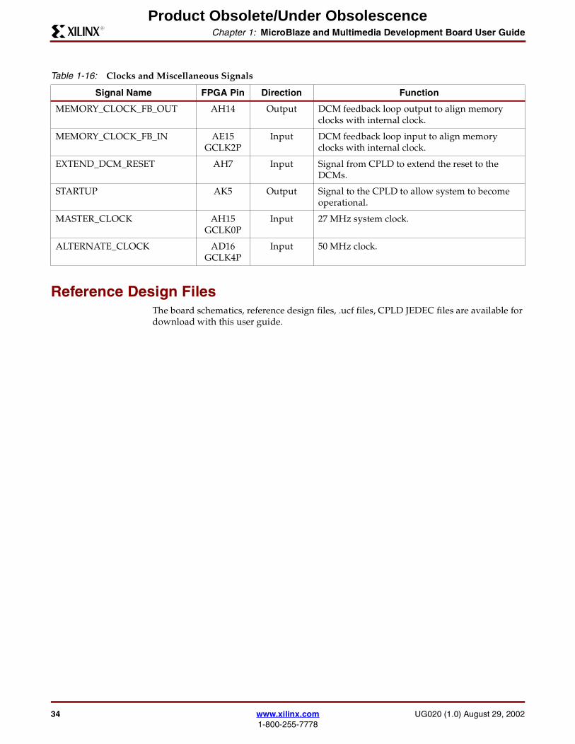
Table 1-16: Clocks and Miscellaneous Signals
Signal Name FPGA Pin Direction Function
MEMORY_CLOCK_FB_OUT AH14 Output DCM feedback loop output to align memory clocks with internal clock.
MEMORY_CLOCK_FB_IN AE15 GCLK2P
Input DCM feedback loop input to align memory clocks with internal clock.
EXTEND_DCM_RESET AH7 Input Signal from CPLD to extend the reset to the DCMs.
STARTUP AK5 Output Signal to the CPLD to allow system to become operational.
MASTER_CLOCK AH15 GCLK0P
Input 27 MHz system clock.
ALTERNATE_CLOCK AD16 GCLK4P
Input 50 MHz clock.
Product Obsolete/Under Obsolescence


