Migrating from AT89C51RB2/RC2/RD2/ED2/IC2/ID2 to AT89LP51RB2/RC2/RD2/ED2/IC2/ID2 New Features • SIngle Clock Cycle per Byte Fetch with 20 MIPS Throughput at 20MHz Clock Frequency • 12 Clock Instruction Compatibility Mode • DSP Extensions with 40-bit 16x16 MAC • Enhanced Dual Data Pointers • 4K Bytes of EEPROM Data Memory with 32-byte Page Programming (AT89LP51ED2 and AT89LP51ID2 Only) • 512 Bytes of User Signature Array • SPI-based In-System Programming in addition to Serial Bootloader • Enhanced Modes on Timer 0 and 1, including PWM • TWI on AT89LP51RB2/RC2/RD2/ED2 • Edge or Level Triggered Keyboard Interrupts • Shared Peripheral Prescaler • Software Reset • Selectable Polarity External Reset Pin • Internal 8.0 MHz Auxiliary Oscillator • Selectable HIgh and Low Power Crystal Oscillator • Use Internal Oscillator for OSCB Source (AT89LP51IC2/ID2 Only) • Configurable I/O Port Modes per Port Pin – Quasi-bidirectional (80C51 Style) – Input-only (Tristate) – Push-pull CMOS Output – Open-drain – Enable Strong Pull-ups on Port 0 • 10-bit ADC/DAC with Temperature Sensor • Dual Analog Comparators with Internal Reference • On-Chip Debug Interface • Up to 40 Programmable I/O Lines • 40-pin PDIP Package Option for AT89LP51RD2/ED2/IC2 • 44-pad QFN/MLF Package Option for all devices • Wide Operating Voltage 2.4–5.5V 1. Introduction The purpose of this application note is to help users convert existing designs from the Atmel AT89C51RB2/RC2/RD2/ED2/IC2/ID2 family to the Atmel AT89LP51RB2/RC2/RD2/ED2/IC2/ID2 family. Within this document AT89LP51xx2 will refer to any one of AT89LP51RB2/RC2/RD2/ED2/IC2/ID2 while AT89C51xx2 will refer to the older AT89C51RB2/RC2/RD2/ED2/IC2/ID2. AT89LP51xx2 is meant as a drop-in replacement for AT89C51xx2. The AT89LP51xx2 product includes both sin- gle-cycle (Fast) and classic 12-Clock (Compatibility) execution modes. Compatibility mode can ease the migration process for legacy designs with little or no software changes. For users looking for more performance, Fast mode and other new features 8051 Flash Microcontroller Application Note 3716A–MICRO–10/11
Transcript
8051 Flash Microcontroller
Application Note
3716A–MICRO–10/11
Migrating from AT89C51RB2/RC2/RD2/ED2/IC2/ID2 to AT89LP51RB2/RC2/RD2/ED2/IC2/ID2
New Features• SIngle Clock Cycle per Byte Fetch with 20 MIPS Throughput at 20MHz Clock Frequency• 12 Clock Instruction Compatibility Mode• DSP Extensions with 40-bit 16x16 MAC• Enhanced Dual Data Pointers• 4K Bytes of EEPROM Data Memory with 32-byte Page Programming (AT89LP51ED2
and AT89LP51ID2 Only)• 512 Bytes of User Signature Array• SPI-based In-System Programming in addition to Serial Bootloader• Enhanced Modes on Timer 0 and 1, including PWM• TWI on AT89LP51RB2/RC2/RD2/ED2• Edge or Level Triggered Keyboard Interrupts• Shared Peripheral Prescaler• Software Reset• Selectable Polarity External Reset Pin• Internal 8.0 MHz Auxiliary Oscillator• Selectable HIgh and Low Power Crystal Oscillator• Use Internal Oscillator for OSCB Source (AT89LP51IC2/ID2 Only)• Configurable I/O Port Modes per Port Pin
– Quasi-bidirectional (80C51 Style)– Input-only (Tristate)– Push-pull CMOS Output– Open-drain– Enable Strong Pull-ups on Port 0
• 10-bit ADC/DAC with Temperature Sensor• Dual Analog Comparators with Internal Reference• On-Chip Debug Interface• Up to 40 Programmable I/O Lines• 40-pin PDIP Package Option for AT89LP51RD2/ED2/IC2• 44-pad QFN/MLF Package Option for all devices• Wide Operating Voltage 2.4–5.5V
1. IntroductionThe purpose of this application note is to help users convert existing designs from theAtme l AT89C51RB2/RC2/RD2/ED2/ IC2 / ID2 fami l y to the A tme lAT89LP51RB2/RC2/RD2/ED2/IC2/ID2 family. Within this document AT89LP51xx2will refer to any one of AT89LP51RB2/RC2/RD2/ED2/IC2/ID2 while AT89C51xx2 willrefer to the older AT89C51RB2/RC2/RD2/ED2/IC2/ID2. AT89LP51xx2 is meant as adrop-in replacement for AT89C51xx2. The AT89LP51xx2 product includes both sin-gle-cycle (Fast) and classic 12-Clock (Compatibility) execution modes. Compatibilitymode can ease the migration process for legacy designs with little or no softwarechanges. For users looking for more performance, Fast mode and other new features
are available to meet their needs. This application note describes the AT89LP51xx2 memories,new and enhanced features, and SFR mapping and register differences. Some assembly codeexamples are provided. More detailed information can be found in the AT89LP51RB2/RC2/IC2and AT89LP51RD2/ED2/ID2 datasheets.
Note that the Two-Wire Interface originally found only on AT89C51IC2/ID2 is now also presenton AT89LP51RB2/RC2/RD2/ED2. Users o f AT89C51IC2 / ID2 can m ig ra te toAT89LP51RC2/ED2 instead of AT89LP51IC2/ID2 if they do not use the second oscillator(OSCB) feature.
2. Getting StartedTo get started with an AT89C51xx2 to AT89LP51xx2 migration, follow these steps:
1. Obtain an updated programming driver
– Check if your existing device programmer has a device driver for the AT89LP51xx2. If your programmer does not support the AT89LP51xx2 you may need to find an alternate solution.
– If you are solely using a Bootloader-based programming solution, you may need to find a programmer using the SPI-based interface or an OCD Debug solution to take full advantage of the enhanced features. See Section 3.1 “Configuration Fuses” on page 4.
2. Determine if you want to use 12-Clock Compatibility mode or Single-Cycle Fast mode
– Compatibility mode provides the easiest migration because instruction/peripheral timing is maintained. In most cases no changes to the software are required. See Section 4.1 “Migrating to Compatibility Mode” on page 6.
– Fast mode provides increased performance or lower power, but at the expense of some software changes. See Section 4.2 “Migrating to Fast Mode” on page 6.
3. If migrating to Fast mode, update fixed timings such as baud rates or timer overflows
– Refer to Section 7. “System Clock” on page 12.
– Refer to Section 10. “Timers” on page 19.
– Refer to Section 11. “Watchdog” on page 21.
– Refer to Section 12. “Serial Interfaces” on page 22.
4. Reconfigure the I/O pin modes, if desired
– By default I/O pins operate compatible to AT89C51xx2. The I/O mode can be updated per port pin in software for greater flexibility. See Section 8. “I/O Ports” on page 14.
5. Make sure the reset pin is active high
– The POL pin (formerly EA) must be pulled high to ensure an AT89C51xx2 compatible reset. See Section 6. “Reset” on page 12.
– Applications with EA low are not supported. However, external execution is still possible for some addresses even on the 64KB AT89LP51RD2/ED2/ID2 without using EA. See Section 5. “Memory Access” on page 9.
6. Configure the device, if desired
– The AT89LP51xx2 supports 15 more fuse options than AT89C51xx2. An SPI-based programmer is required to change these fuses. See Section 3.1 “Configuration Fuses” on page 4.
23716A–MICRO–10/11
Migrating from 89C51xx2 to 89LP51xx2
Migrating from 89C51xx2 to 89LP51xx2
3. Flash/EEPROM ProgrammingThe AT89LP51xx2 microcontroller does not support high-voltage parallel programming. Insteadan SPI-based interface compatible with other AT89LP devices is provided. Users with third-partyparallel programmers will need to update their programmer with the appropriate AT89LP51xx2serial driver if available. However, the serial bootloader protocol is compatible with the existingAT89C51xx2. Existing bootloader-based programmers wil l be able to program theAT89LP51xx2 with an AT89C51xx2 driver, although it is recommended that drivers be updatedto make use of the new features on the AT89LP51xx2. The flash programming differences aresummarized in Table 3-1.
Note: 1. The device signature is stored in the Atmel Signature Array on AT89LP51xx2 and in the XROW on AT89C51xx2. Locations 30-31H and 60-61H have the same signature value in both AT89C51xx2 and AT89LP51xx2. Locations 00-02H are provided for compatibility with other AT89LP devices.
Users migrating from AT89C51xx2 to AT89LP51xx2 devices will notice the following changes tothe programming interface:
1. The Hardware Security Byte (HSB) is accessible only through the Bootloader interface. The SPI-based interface accesses these bits individually.
2. The Bootloader configuration bytes (BSB, SSB and SBV) are located in the User Signa-ture space at different addresses than AT89C51xx2. This affects only the SPI-based interface and not the Bootloader.
3. The AT89LP51xx2 has a half-page buffer of 64 bytes. Therefore Page mode com-mands accept only 64 bytes of data. However, Bootloader programming still allows a full 128 bytes to be sent.
4. Individual reprogramming of bytes is not possible. On AT89LP51xx2 one page is the smallest erasable quantity whereas on AT89C51xx2 it was one byte. Programming algorithms must erase and write an entire page when even only a single byte needs to change. This affects only the SPI-based interface and not the Bootloader; however, the bootloader is most efficient when working with full pages.
Table 3-1. Summary of Programming Differences on AT89LP51xx2
5. The Data[1] byte of the Program OSC Fuse command is changed from 20h on AT89C51IC2/ID2 to 10h on AT89LP51IC2/ID2.
6. The AT89LP51xx2 has a selectable polarity RST pin. Existing AT89C51xx2 drivers expect the reset to have active-high polarity. In most existing applications the EA pin is tied high, so dropping in an AT89LP51xx2 will result in an active-high reset. See Sec-tion 6. “Reset” on page 12.
In addition to the above changes, the AT89LP51xx2 also supports the following new features:
1. The AT89LP51xx2 includes a User Signature Array for storing up to 512 bytes of user ID, revision, configuration or other nonvolatile information. This information can be read/written from the application code. The BSB, SBV and SSB bytes are stored in this array. The full array is accessible to the SPI interface; however, only the first 256 bytes can be programmed through the Bootloader.
2. The AT89LP51xx2 supports 19 User Configuration Fuses for configuring the default behavior of the device. See Section 3.1 for more information. The fuses beyond the 4 used by the AT89C51xx2 are not accessible by the Bootloader. These fuses may require configuration before placing the device in system.
3. SPI-programming can be disabled during warm resets by clearing the ISP Enable Fuse. When this fuse is disabled, programming is only available by asserting RST at power-up (cold reset). This fuse does not affect the bootloader functionality.
4. The AT89LP51ED2/ID2 supports page programming of the EEPROM with up to 32 bytes written per operation.
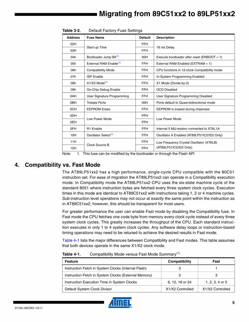
3.1 Configuration FusesThe AT89LP51xx2 includes nineteen User Configuration Fuses for configuring the defaultbehavior of the device. Most fuses can only be changed by an SPI-based device programmer orOCD Debug solution that supports this feature. Four fuses are supported by the bootloader andFlash API. The default fuse settings are listed in Table 3-2. These settings were chosen to pro-v ide the greatest compat ib i l i ty wi th the prev ious AT89C51xx2 device. See theAT89LP51RB2/RC2/IC2 and AT89LP51RD2/ED2/ID2 datasheets for more detailed information.
For existing applications that use an external clock source instead of a crystal or resonator, it isrecommended that the CSA1 fuse (address 01H) be cleared to 00H to select the external clockconfiguration. This configuration provides better performance at higher frequencies than drivingthe on-chip crystal oscillator in open loop mode. Changes to this fuse will only take affect whenthe power is cycled off and on.
For the AT89LP51IC2/ID2 devices the second oscillator source is also configurable with theCSB1-0 fuses (addresses 11–12H).
Compatibility/Fast Mode is selected by setting/clearing the Compatibility Mode Fuse at address04H. Compatibility mode is enabled by default. Users wishing to migrate to Fast mode mustclear this fuse.
Other features can be enabled/disabled by changing their respective fuses.
Table 3-2. Default Factory Fuse Settings
Address Fuse Name Default Description
00HClock Source A
FFHHigh Speed Crystal Oscillator (XTALA)
01H FFH
43716A–MICRO–10/11
Migrating from 89C51xx2 to 89LP51xx2
Migrating from 89C51xx2 to 89LP51xx2
Note: 1. This fuse can be modified by the bootloader or through the Flash API
4. Compatibility vs. Fast ModeThe AT89LP51xx2 has a high performance, single-cycle CPU compatible with the 80C51instruction set. For ease of migration the AT89LP51xx2 can operate in a Compatibility executionmode. In Compatibility mode the AT89LP51xx2 CPU uses the six-state machine cycle of thestandard 8051 where instruction bytes are fetched every three system clock cycles. Executiontimes in this mode are identical to AT89C51xx2 with instructions taking 1, 2 or 4 machine cycles.Sub-instruction level operations may not occur at exactly the same point within the instruction asin AT89C51xx2; however, this should be transparent for most users.
For greater performance the user can enable Fast mode by disabling the Compatibility fuse. InFast mode the CPU fetches one code byte from memory every clock cycle instead of every threesystem clock cycles. This greatly increases the throughput of the CPU. Each standard instruc-tion executes in only 1 to 4 system clock cycles. Any software delay loops or instruction-basedtiming operations may need to be retuned to achieve the desired results in Fast mode.
Table 4-1 lists the major differences between Compatibility and Fast modes. This table assumesthat both devices operate in the same X1/X2 clock mode.
10H Oscillator Select(1) FFH Oscillator A Enabled (AT89LP51IC2/ID2 Only)
11HClock Source B
FFH Low Frequency Crystal Oscillator (XTALB)
(AT89LP51IC2/ID2 Only)12H FFH
Table 3-2. Default Factory Fuse Settings
Address Fuse Name Default Description
Table 4-1. Compatibility Mode versus Fast Mode Summary(1)
Feature Compatibility Fast
Instruction Fetch in System Clocks (Internal Flash) 3 1
Instruction Fetch in System Clocks (External Memory) 3 3
Instruction Execution Time in System Clocks 6, 12, 18 or 24 1, 2, 3, 4 or 5
Default System Clock Divisor X1/X2 Controlled X1/X2 Controlled
53716A–MICRO–10/11
Note: 1. Cycle times are given in internal system clocks. These are the same as oscillator periods for X2 mode. For X1 mode, multiple system clocks by two to get equivalent oscillator periods.
4.1 Migrating to Compatibility ModeMost users migrating legacy software from AT89C51xx2 to AT89LP51xx2 in Compatibility modeshould not need to make any changes to their software provided that the application code doesnot activate any of the new register bits in existing registers listed in Section 9.2 “Modified Regis-ters” on page 16 in such a manner as to change the behavior of the application. In most casesthis should not be an issue.
For users of AT89C51IC2/ID2 that manipulate the TWI lines directly through the port register, anupdate is required because these lines are mapped to P4.1-0 instead of PI2C.1-0.
In the rare case a user has a custom software bootloader or application that uses the low-levelregister interface (FCON) instead of the Flash API, changes to the code will be required. SeeSection 5.1.1 “In-Application Programming” on page 9.
Users willing to update their software can take advantage of any of the new peripheral featuresfound on the AT89LP51xx2 in Compatibility mode while maintaining standard 8051 instructiontiming.
4.2 Migrating to Fast ModeUsers migrating legacy software from AT89C51xx2 to AT89LP51xx2 in Fast mode generallymust make a small number of changes to their application code and possibly a hardware-relatedchange to the clock frequency to maintain the same behavior. These changes are described inthe following sections. Users willing to further update their software can take advantage of any ofthe new peripheral features found on the AT89LP51xx2 plus the greater performance of the Fastmode CPU.
For users of AT89C51IC2/ID2 that manipulate the TWI lines directly through the port register, anupdate is required because these lines are mapped to P4.1-0 instead of PI2C.1-0.
In the rare case a user has a custom software bootloader or application that uses the low-levelregister interface (FCON) instead of the Flash API, more changes to the code will be required.See Section 5.1.1 “In-Application Programming” on page 9.
4.2.1 System Frequency and Clock DivisionOne of the first decisions that users migrating designs from AT89C51xx2 to AT89LP51xx2 inFast mode must make is at what frequency to run the AT89LP51xx2. By default theAT89LP51xx2 in Fast mode is at least 3 times faster than the AT89C51xx2 in the same X1/X2mode, meaning it fetches bytes from memory in one-third the time. Therefore the maximumoperating frequency may be lower in Fast mode than if the AT89LP51xx2 was operating in Com-patibility mode. Users must check that the desired frequency of the crystal or clock driver does
Table 4-1. Compatibility Mode versus Fast Mode Summary(1)
Feature Compatibility Fast
63716A–MICRO–10/11
Migrating from 89C51xx2 to 89LP51xx2
Migrating from 89C51xx2 to 89LP51xx2
not exceed the maximum specification for AT89LP51xx2. If so, the frequency must be scaleddown.
The AT89LP51xx2 supports the X1/X2 feature of AT89C51xx2. This feature determines if theinternal system clock is divided by two or not. The easiest migration path is to maintain the samemode on AT89LP51xx2 as was used on AT89C51xx2. This will preserve the timing of all periph-eral features that depend only on the system clock such as Mode 2 of the UART. However, thebest performance in terms of throughput and power is achieved only in X2 mode.
When migrating from X1 to X2 mode the system clock is no longer divided-by-2. Therefore if thesame external clock frequency is maintained from AT89C51xx2 in X1, the AT89LP51xx2 in X2mode will operate at an internal system clock that is twice as fast as on the AT89C51xx2. Fea-tures that depend only on the internal system clock rate include the UART in modes 0 and 2,Timer 2 in Baud Rate or Clock Out modes and the external memory interface timing. To maintainthe same timing using the UART in these modes or when the compare values for Timer 2 cannotbe updated, the user can do either of the following:
• Cut the external clock frequency in half, or
• Set the Timer Prescaler for divide-by-two in the CLKREG SFR and enable prescaling on the UART, Timer 2, etc. through the CKCON0 and CKCON1 registers.
For timing on the external memory interfaces, see Section 5.1 “Program Memory” on page 9 andSection 5.2.1 “External Data Memory” on page 10.
Another difference in Fast mode is that the PCA, Timer 0, 1, 2 and the Watchdog by defaultcount at a rate equal to the internal system clock instead of every sixth system clock. The count-ing behavior is made compatible with AT89C51xx2 by setting the timer prescaler in CLKREG todivide-by-6 (the default value) and then enabling the prescaler for a specific timer in CKCON0. Ifthe mode is also changed from X1 to X2, then either the frequency must be halved or the pres-caler should be doubled to divide-by-12. If one of the these steps is taken, any time-out periodsor timer-generated baud rates will be maintained without any further changes.
• Example 1: AT89C51xx2 at external 24 MHz X1 or 12 MHz X2
The AT89C51xx2 runs at an internal frequency of 12 MHz after the default divider of 2. Theuser chooses to run the AT89LP51xx2 at external 12 MHz X2. This maintains the sameinternal system clock speed, therefore the UART in modes 0 and 2 or Timer 2 in Baud Rateor Clock Out modes will still function as expected. Timers 0 and 1 and the Watchdog willcount six times faster, so the timer prescaler is set to divide by 6 to preserve any time-outperiods or baud rates:
• Example 2: AT89C51xx2 at external 11.0592 MHz X1
The user chooses to maintain the existing external frequency of 11.0592 Mhz. The userkeeps the X1 clock divider to maintain the UART and Timer 2 in the modes mentionedabove. The user also wants to maintain the baud rate generated by Timer 1 and sets theprescaler to divide-by-6:
Another user also maintains the existing external frequency, but the system is not using theUART or Timer 2 in any of the modes mentioned above, so the user disables the clockdivider (X2). The user wants to maintain the baud rate generated by Timer 1 and sets theprescaler to divide-by-12:
One advantage of Fast mode is that it allows the AT89LP51xx2 to provide the same instructionthroughput as the AT89C51xx2 at a much lower frequency, thereby reducing overall power con-sumption. AT89LP51xx2 Fast mode is guaranteed to have at least 3 times the throughput ofAT89C51xx2 at the same frequency and X1/X2 mode. Therefore the frequency of theAT89LP51xx2 can be reduced up to 3 times as compared to the AT89C51xx2 without reducingperformance. However, doing so will affect the behavior of the peripherals. If the clock divider isdisabled (X1 to X2), Fast mode is guaranteed to have at least 6 times the throughput, e.g. canoperate 6 times slower than AT89C51xx2 in X1 mode.
• Example 3: AT89C51xx2 at external 24 MHz X1 or 12 MHz X2
The user chooses to run the AT89LP51xx2 at external 4 MHz with no divider (X2). The min-imum instruction throughput is the same as AT89C51xx2. The UART in modes 0 and 2 willbe slower and Timer 2 in Baud Rate or Clock Out modes will need a shorter period to main-tain the same rate. Timers 0 and 1 and the Watchdog will only count twice as fast asAT89C51xx2, so the timer prescaler is set to divide by 2 to preserve any time-out periods orbaud rates:
In conclusion, the external system frequency, system clock divider and timer prescaler are allavailable as parameters for maintaining timing compatibility between AT89LP51xx2 in Fastmode and AT89C51xx2.
4.2.2 Software DelaysDelays generated in the application code by executing instructions will have different lengthsbetween Fast and Compatibility modes. These type of routines must be updated.
• Example: DJNZ Wait Loop
A simple example is the DJNZ wait loop, which waits for a specified count:
MOV R7, #N
WAITN: DJNZ R7, WAITN ; loop N times
On AT89C51xx2 and AT89LP51xx2 in Compatibility mode, the DJNZ instruction requires 12system clocks. In Fast mode, the AT89LP51xx2 executes DJNZ in only 3 system clocks,thus N would need to be 4 times larger to generate the same delay at the same system fre-quency and X1/X2 mode.
4.2.3 ALEIn Fast mode the ALE signal toggles at a rate of half the system clock with 50% duty cycle ascompared to one third of the system clock at 33% duty cycle in Compatibility mode. Applicationsthat make use of ALE at board level may need to be adjusted accordingly. For applications thatdo not use ALE, or use it only for external memory, it is recommended that ALE be disabled bysetting the AO bit in AUXR for reduced power consumption.
83716A–MICRO–10/11
Migrating from 89C51xx2 to 89LP51xx2
Migrating from 89C51xx2 to 89LP51xx2
4.2.4 TimersIf the same timer rate as AT89C51xx2 is not maintained as detailed above in Section 4.2.1, thetimer reload or compare values will need to be scaled accordingly. See Section 10. on page 19
4.2.5 WatchdogIf the same timer rate as AT89C51xx2 is not maintained as detailed above in Section 4.2.1, theWatchdog may need to either be reset more often or have its period lengthened with the watch-dog prescaler settings in WDTPRG. See Section 11. on page 21.
4.2.6 UART/SPI/TWIIf the same baud rate as AT89C51xx2 is not maintained as detailed above in Section 4.2.1, thebaud rate setting may need to be scaled accordingly. See Section 12. on page 22.
5. Memory AccessThe AT89LP51xx2 supports the same memory spaces found on the AT89C51xx2. The programmemory has support for 24/32/64K bytes of on-chip Flash program memory and support for upto 40/32K bytes of external program memory using the standard 80C51 interface. The datamemory has 256 bytes of internal RAM and 128 bytes of Special Function Register I/O space,with support for up to 64K bytes of external data memory also using the standard 80C51 inter-face. Applications that use these memory spaces should not need to be updated in Compatibilitymode unless they want to take advantage of the additional features on the AT89LP51xx2.
5.1 Program MemoryThe AT89LP51xx2 supports both internal and external program memory. Applications that onlyuse external program memory, by tying the EA pin low, are not supported on the AT89LP51xx2.External program memory is only available at addresses 8000H–FFFFH (6000H–FFFFH) forAT89LP51RC2/IC2 (AT89LP51RB2). For AT89LP51RD2/ED2/ID2 external program memory isallowed at 8000H–FFFFH only when bank switching is enabled by setting the FBS bit in BMSEL.
In Compatibility mode there is no difference when executing from internal versus external pro-gram memory. In Fast mode, two wait states must be inserted for every external fetch. Thereforeinstructions executed from external memory in Fast mode are exactly three times longer thaninstructions executed from internal memory. This may play an important role when selecting theoperating frequency as detailed in Section 4.2.1 on page 6. Furthermore, if switching from X1 toX2 mode, the external memory interface will fetch at twice the rate of X1 mode at the same fre-quency. To maintain the same external memory timing the user can do either of the following:
• Cut the external frequency in half, or
• Enable divide-by-two (X1) for the system clock in the CKCON0 SFR before accessing external memory.
5.1.1 In-Application ProgrammingSelf-programming of the Flash Code memory, fuses and configuration bytes is supportedthrough the same Flash API as found on AT89C51xx2. Legacy code that uses the Flash APIdoes not require updating. In the rare case a user has a custom software bootloader or applica-tion that uses the low-level register interface (FCON) instead of the Flash API, changes to thecode will be required as there are some differences between AT89LP51xx2 and AT89C51xx2 inthis aspect. The low-level interface is described in the AT89LP51RB2/RC2/IC2 and AT89LP51RD2/ED2/ID2 datasheets whereas it was omitted from the AT89C51xx2 documentation. This
93716A–MICRO–10/11
type of migration is beyond the scope of this document. Please contact the Atmel support teamdirectly if questions arise.
5.1.2 Signature Array & FusesThe AT89LP51xx2 makes the 128-byte Atmel Signature, 512-byte User Signature and 19 UserFuses readable and writable from the application code (Atmel Signature is read-only). For com-patibility reasons only a subset of these are accessible through the bootloader and Flash API.Users willing to update their code can take full advantage of these resources through the low-level interface.
5.2 Data MemoryThe 256 bytes of internal RAM and 128 bytes of Special Function Register I/O space areaccessed in the normal manner. See Section 9. for a list of new or modified registers on theAT89LP51xx2. The external data memory interface may require some tuning for operation inFast mode. EEPROM Page Mode is a new feature available on the AT89LP51ED2/ID2.
5.2.1 External Data MemoryThe external data memory interface of the AT89LP51xx2 is accessed in the same manner as onAT89C51xx2. Some portions of the external memory address space can be redirected towardon-chip memories. By default this redirection is disabled so legacy code can access the entireaddress range. The EXTRAM bit in AUXR can also be used to override any other settings andforce access to external memory. The default value is controlled by the XRAM fuse.
In Compatibility mode, MOVX timing for external memory access is identical to AT89C51xx2. InFast mode the MOVX instruction is faster, meaning a shorter access time to external memory. Ifan existing external memory can support the faster access, then nothing must be done whenmigrating to Fast mode. If not, the timing of MOVX must be lengthened by changing the systemclock and/or wait state settings. The wait states are controlled by the WS bits in AUXR as listedin Table 5-1. The wait states can increase the length of the strobe and also the setup betweenALE and the strobe. Note that each additional wait state adds one clock cycle to the instructionexecution time.
Table 5-2 shows some possible configurations for MOVX timing in Fast mode. The only way toachieve identical timing with Compatibility mode is to cut the system frequency in third and addone wait state. In other configurations the user must select the settings that are nearest enoughto meet the specifications of the system.
Table 5-1. Wait State Effects on MOVX Timing (in System Clocks)
WS1 WS0
RD or WR Strobe WidthALE low to RD or WR
low SetupAccess Time
(setup + width)
Compatibility Fast Compatibility Fast Compatibility Fast
0 0 3 1 1.5 1 4.5 2
0 1 15 2 1.5 1 16.5 3
1 0 3 2 1.5 2 4.5 4
1 1 15 3 1.5 2 16.5 5
103716A–MICRO–10/11
Migrating from 89C51xx2 to 89LP51xx2
Migrating from 89C51xx2 to 89LP51xx2
Note: TOSC is the external oscillator period of the AT89C51xx2
5.2.2 Internal Extra RAMThe AT89LP51RB2/RC2/IC2 (AT89LP51RD2/ED2/ID2) supports 1152 (2048) bytes of internalExtra RAM, 128 (256) bytes more than AT89C51RB2/RC2/IC2 (AT89LP51RD2/ED2/ID2). Thisadditional RAM is accessible by changing the XRS bits in AUXR.
5.2.2.1 Paged AccessOn the AT89C51xx2, only the first 256 bytes of Extra RAM are accessible with the MOVX @Riinstructions. On the AT89LP51xx2 the entire Extra RAM is accessible in a paged manner byusing the PAGE register to select a 256-byte block. Furthermore, the PAGE register can forceMOVX @Ri to use external memory without setting the EXTRAM bit. PAGE addressing isindependent of XRS.
5.2.2.2 Extended StackThe AT89LP51xx2 allows the hardware stack to be located anywhere in Extra RAM by settingthe XSTK bit in AUXR1. The Extended Stack requires the use of the Extended Stack Pointer(SPX) in addition to SP. All stack operations incur a one cycle delay when operating on theextended stack.
5.2.3 EEPROM Data MemoryIn addition to the 64K bytes of external data memory, addresses 0000H–0FFFH of the externaldata memory space are implemented on chip as 4K bytes of nonvolatile EEPROM data memoryon the AT89LP51ED2/ID2. These bytes are only accessible when the EEE bit is set in EECON.This is twice the amount of EEPROM as present on AT89C51ED2/ID2. Note that unlikeAT89C51ED2/ID2, addresses above the EEPROM range will still access external memory whileEEE is set.
A new feature of the AT89LP51ED2/ID2 is page programming of the EEPROM. Page program-ming is controlled by the LDPG bit in EECON. While this bit is set, a write to the EEPROM space
Table 5-2. Configuration Settings for MOVX Timing in Fast Mode
Description
Configuration Settings
Access TimeX2 WS
AT89C51xx2 0 M0 = 0 9 x TOSC
AT89LP51xx2 Compatibility Mode Default 0 0 9 x TOSC
AT89LP51xx2 Fast Mode Default 1 0 2 x TOSC
Nearest to AT89C51xx2 in Fast Mode at Same Frequency
1 3 5 x TOSC
02 8 x TOSC
3 10 x TOSC
Nearest to AT89C51xx2 in Fast Mode at 1/2 Frequency1
2 4 x (2 x TOSC)
3 5 x (2 x TOSC)
0 0 4 x (2 x TOSC)
Compatible to AT89C51xx2 in Fast Mode at 1/3 Frequency 1 1 3 x (3 x TOSC)
Nearest to AT89C51xx2 in Fast Mode at 1/6 Frequency 1 0 2 x (6 x TOSC)
113716A–MICRO–10/11
will not start a programming sequence, but will only load the page buffer. LDPG should becleared before writing the final byte in a page. Up to 32 bytes can be loaded at a time.
• Example: Write a simple pattern in EEPROM data memory
MOV A, R1MOVX @DPTR, A ; load byte to bufferINC DPTR ; next addressINC R1 ; incrementing patternDJNZ R0, LOADANL EECON, #~20H ; clear LDPGMOV A, R1MOVX @DPTR, A ; load last byte and start writeMOV EECON, #0 ; clear EEE
6. ResetThe AT89LP51xx2 has a user-selectable external reset pin. To support this feature the formerExternal Access pin (EA) of the AT89C51xx2 is replaced by the Polarity pin (POL). When thispin is at VCC, the RST pin is active-HIGH with a pull-down resistor; and when this pin is at GND,the RST pin is active-LOW with a pull-up resistor. As a consequence the external access featureis NOT supported on the AT89LP51xx2; however, external execution is still allowed foraddresses 8000H–FFFFH (6000H–FFFFH) on AT89LP51RC2/IC2 (AT89LP51RB2). Externalexecution on AT89LP51RD2/ED2/ID2 is allowed for addresses 8000H–FFFFH when FBS is setin BMSEL. The majority of legacy AT89C51xx2 applications have EA tied high for internal exe-cution. Dropping an AT89LP51xx2 into these applications will result in POL tied high for anAT89C51xx2- compatible active-HIGH reset. If an AT89C51xx2 application has EA tied low, theuser must either modify the board to connect POL to high or disconnect the RST pin from anyboard-level signals.
The POL pin must be driven high or low at all times. It does not have an internal pull-up or pull-down. The level of the POL pin is sampled during power-up. It is not possible to change thepolarity once the device is operational. An active-low reset is recommended for all newapplications.
If In-System Programming is disabled, the only way to program the AT89LP51xx2 is if RST isactive during power-up. ISP is always enabled at power-up and will remain active until the firstdeactivation of RST. Users wishing to further program the device in such a state must have ameans of connecting RST to VCC or GND at power-up, depending on the polarity.
7. System ClockThe system clock source of the AT89LP51xx2 is selectable between the crystal oscillator, anexternally driven clock and an internal 8.0 MHz auxiliary oscillator. In addition the crystal oscilla-tor can operate in either high-power or low-power mode and optionally have an on-chip 5 MΩresistor connected between XTAL1 and GND for improved startup. On the AT89LP51IC2/ID2 asecond oscillator source is also available and is selectable between a low frequency (32KHz)crystal oscillator, an externally driven clock and the internal 8.0 MHz auxiliary oscillator. The
123716A–MICRO–10/11
Migrating from 89C51xx2 to 89LP51xx2
Migrating from 89C51xx2 to 89LP51xx2
clock source and options are controlled by the User Fuses. Section 3.1 “Configuration Fuses” onpage 4.
The AT89LP51xx2 is factory-configured to use the crystal oscillator in high-power mode. Userswanting to switch to low-power mode may need to remove or reduce capacitors on the XTAL1and XTAL2 pins. Applications that use an external clock source should select the external clockconfiguration instead of driving the oscillator in open-loop mode. In external clock mode, theXTAL2 pin is available as a general purpose I/O, P4.7.
The AT89LP51xx2 includes an on-chip 8.0 MHz auxiliary RC oscillator that is used for someinternal functions. It is also available as a system clock source. The oscillator has accuracy of±2.5% to enable UART communications and may be user calibrated to other frequencies near8.0 MHz. In internal oscillator mode, XTAL1 and XTAL2 pins are available as a general purposeI/Os P4.6 and P4.7, respectively.
7.1 Clock DividerThe System Clock Divider scales the internal system clock versus the oscillator clock source.The divider is controlled by the CKRL register. In addition the system clock frequency may bedivided by 2 from the externally supplied XTAL1 frequency for compatibility with standard 8051sin X1 mode (12 clocks per machine cycle). The divide-by-2 can be disabled to operate in X2mode (6 clocks per machine cycle) or the clock may be further divided to reduce the operatingfrequency. If the divide-by-2 is disabled, make sure that the new system clock frequency is stillwithin the valid operating range. The X1/X2 feature is maintain in Fast mode. See “System Fre-quency and Clock Division” on page 6 for more information.
• Example: Disable Divide-by-2 (Enable X2 Mode)
ORL CKCON0, #01H ; set X2
7.2 Timer PrescalerA common prescaler is available to divide the time base for Timer 0, Timer 1, Timer 2, PCA andthe Watchdog. The TPS3-0 bits in the CLKREG SFR control the prescaler. In Compatibility modeTPS3-0 defaults to 0101B, which causes the timers to count once every machine cycle. Thecounting rate can be adjusted linearly from the system clock rate to 1/16 of the system clock rateby changing TPS3-0. In Fast mode TPS3-0 also defaults to 0101B; however, the prescaler mustbe enabled for a particular peripheral by settings its ?X2 bit in CKCON0/1. Note that in Fastmode the prescaler is also available for the SPI and TWI.
TPS 1+---------------------= Fast Mode and ?X2 = 1
133716A–MICRO–10/11
8. I/O PortsThe P0, P1, P2, P3 and P4 I/O port pins of the AT89LP51xx2 may be independently configuredin four different modes:
• Quasi-bidirectionalStandard 80C51 I/O with strong, medium and weak pull-ups good for general bidirectional use.
• Input OnlyThe I/O is tristated for high impedance input. This mode reduces power for low-level inputs by removing the pull-ups; however, the input should not be left floating or higher power consumption may occur.
• Push-Pull OutputThe I/O provides a full CMOS output driver with larger current sourcing capabilities than quasi-bidirectional.
• Open-DrainThe I/O pull-ups are disabled. An external pull-up is required to use the I/O to output a high level. Open-Drain is most useful for wired-AND type buses.
The default port settings depend on the Tristate-Port User Fuse. When the fuse is enabled, allport pins on P1, P2 and P3 default to input-only mode after reset. When the fuse is disabled, allport pins on P1, P2 and P3 default to quasi-bidirectional mode after reset and are weakly pulledhigh. P0 always defaults to open-drain mode. P4.4–5 always default to quasi-bidirectional mode.P4.0–1 always default to open-drain. The other pins of P4 obey the fuse. P0 can be configuredto have internal pull-ups by placing it in quasi-bidirectional or output modes. This can reducesystem cost by removing the need for external pull-ups on Port 0.
• Example: Enable Pull-ups on Port 0
MOV P0M0, #00H ; all P0 pins quasi-bidirectional
Port configuration is set by the PxM0 and PxM1 registers and is independently configurable foreach pin. Ports pins using bidirectional signals should not be set to Input Only or Push-Pull Out-put modes as these modes are unidirectional..
P0 and P2 do not require configuration to use the external memory interface. Addresses willautomatically be output in push-pull mode and P0 is automatically tristated during instruction ordata read. ALE and PSEN always default to quasi-bidirectional mode. The RD and WR strobes;however, will be configured with P3. To use external data memory P3 must be configuredaccordingly, either by clearing the Tristate-Port Fuse or writing the correct P3M0 and P3M1 bits.
The AT89LP51xx2 provides an additional I/O port P4. Note that this P4 differs from the P4 origi-nally offered on the obsoleted PLCC68 and VQFP64 packages of AT89C51RD2/ED2. Pins P4.2and P4.4–P4.7 replace the normally dedicated XTAL2B, ALE, PSEN, XTAL1(A) and XTAL2(A)pins of the AT89LP51xx2. These pins can be used as additional I/Os depending on the configu-ration of the clock and external memory as listed in Table 8-2. Pins P4.1-0 are the TWI lines that
Table 8-1. Configuration Modes for Port x Pin.y
PxM1.y PxM0.y Port Mode
0 0 Quasi-bidirectional
0 1 Input Only (High Impedance)
1 0 Push-pull Output
1 1 Open-Drain Output
143716A–MICRO–10/11
Migrating from 89C51xx2 to 89LP51xx2
Migrating from 89C51xx2 to 89LP51xx2
were previously called PI2.1-0 on AT89C51IC2/ID2. P4.3 is the data line for the On-Chip Debugdatabase.
Note: 1. For AT89LP51IC2/ID2 the OSCA pins dependent only on the OSCA source selection and not on whether OSCA is enabled or not.
9. Special Function RegistersThis section lists the Special Function Registers (SFRs) that are new or modified inAT89LP51xx2 from those in AT89C51xx2.
9.1 SFR MappingThe highlighted SFR locations are new registers for the AT89LP51xx2 device.
Table 8-2. Configurations for Additional I/Os
Pin Function Configuration Required for General I/O Use
P4.0 SCL None. (Replaces PI2.0 in AT89C51IC2/ID2)
P4.1 SDA None. (Replaces PI2.1 in AT89C51IC2/ID2)
P4.2 XTAL2BInternal 8.0 MHz oscillator or external clock selected for OSCB; or OSCB disabled (AT89LP51IC2/ID2 Only)
P4.3 DDA OCD Disabled
P4.4 ALE No external memory and AO = 1
P4.5 PSEN No external program memory
P4.6 XTAL1(A) Internal 8.0 MHz oscillator selected for OSCA(1)
P4.7 XTAL2(A) External clock or internal 8.0 MHz oscillator selected for OSCA(1)
9.2 Modified RegistersThe following registers are modified in their bit definitions from AT89C51xx2. For more detailedinformation see the AT89LP51RB2/RC2/IC2 and AT89LP51RD2/ED2/ID2 datasheets.
.
.
9.3 New RegistersThe following registers are additional registers not found in AT89C51xx2. For more detailedinformation see the AT89LP51RB2/RC2/IC2 and AT89LP51RD2/ED2/ID2 datasheets.
Notes: 1. Reset value is FFH when Tristate-Port Fuse is enabled and 00H when disabled
2. Reset value is C7H when Tristate-Port Fuse is enabled and 03H when disabled
10. TimersThe timer counting rate of Timer 0, Timer 1, Timer 2 and the PCA is controlled by the timer pres-caler. The timer prescaler defaults to one sixth of the system clock, the same rate asAT89C51xx2. In Compatibility Mode the prescaler always affects the timer operation. No soft-ware changes to the timers should be required when migrating legacy software to CompatibilityMode. In Fast mode the prescaler is disabled for all timers and the timers count at the systemclock rate. See “System Frequency and Clock Division” on page 6. The user can control thebehavior of the timers with the timer prescaler (TPS) settings in CLKREG, the clock divider set-ting (CKRL) and the individual clock control bits in CKCON0. In Fast mode each CKCON0 bit(T0X2, T1X2, T2X2 or PCAX2) enables/disables the prescaler for each timer individually. See“Timer Prescaler” on page 13.
Table 10-1 lists several possible configurations for the Timers.
Full timer rate compatibility with AT89C51xx2 for Timer 2 in Baud Rate or Clock-Out modes orPCA with CPS=1 can only be maintained in AT89LP51xx2 Fast mode in the following two cases:
• If AT89LP51xx2 operates at the same frequency as AT89C51xx2
– If AT89C51xx2 uses X1 mode, then on AT89LP51xx2 T2X2/PCAX2 = X2
– If AT89C51xx2 uses X2 mode, then on AT89LP51xx2 T2X2/PCAX2 = 0 and X2 = 1
• If AT89LP51xx2 operates at half the frequency of AT89C51xx2
– Then T2X2/PCAX2 = 0 and X2 = 1.
Otherwise the reload values may need to be scaled accordingly. For example, if theAT89LP51xx2 operates at the same frequency as AT89C51xx2 but CDV = 0, the reload valuefor Timer 2 in Baud Rate or Clock-Out mode must be twice as long to overflow at the same rate.
Table 9-28. Port Configuration Registers
Port Register Address Reset Register Address Reset
Table 10-1. Configuration Settings for Compatible Timer Rates (CKRL=255)
Timer 0 or Timer 1
Timer 2 in Auto-Reload or Capture ModesPCA with CPS=0
Configuration Settings
Timer RateTnX2 / PCAX2 X2 TPS
AT89C51xx20
0 – fC51 / 12
1 – fC51 / 6
1 1 – fC51 / 12
AT89LP51xx2 Compatibility Mode Default0
0 5 fOSC / 12
1 5 fOSC / 6
1 1 5 fOSC / 12
AT89LP51xx2 Fast Mode Default
00 – fOSC / 2
1 – fOSC / 1
10 5 fOSC / 12
1 5 fOSC / 6
AT89LP51xx2 Fast Mode Compatible to AT89C51xx2 X1 at Same Frequency (fOSC = fC51)
1 0 5 fOSC / 12 =
fC51 / 121 1 11
AT89LP51xx2 Fast Mode Compatible to AT89C51xx2 X2 at Same Frequency (fOSC = fC51)
1 0 2 fOSC / 6 =
fC51 / 61 1 5
AT89LP51xx2 Fast Mode Compatible to AT89C51xx2 X1 at Half Frequency (fOSC = fC51÷2)
1 0 2 fOSC / 6 =
fC51 / 121 1 5
AT89LP51xx2 Fast Mode Compatible to AT89C51xx2 X2 at Half Frequency (fOSC = fC51÷2)
1 1 2fOSC / 3 =
fC51 / 6
AT89LP51xx2 Fast Mode Compatible to AT89C51xx2 X1 at One-Sixth Frequency (fOSC = fC51÷6)
0 0 – fOSC / 2 =
fC51 / 121 1 1
AT89LP51xx2 Fast Mode Compatible to AT89C51xx2 X2 at One-Sixth Frequency (fOSC = fC51÷6)
0 1 –fOSC / 1 =
fC51 / 6
Timer 2 in Baud Rate or Clock-Out Modes
PCA with CPS=1TnX2 / PCAX2 X2 TPS Timer Rate
AT89C51xx20
0 – fC51 / 2
1 – fC51 / 1
1 1 – fC51 / 2
AT89LP51xx2 Compatibility Mode Default0
0 – fOSC / 2
1 – fOSC / 1
1 1 – fOSC / 2
AT89LP51xx2 Fast Mode Default
00 – fOSC / 2
1 – fOSC / 1
10 – fOSC / 4
1 – fOSC / 2
203716A–MICRO–10/11
Migrating from 89C51xx2 to 89LP51xx2
Migrating from 89C51xx2 to 89LP51xx2
Note: fC51 is the XTAL1 frequency of the AT89C51xx2. fOSC is the XTAL1 frequency of the AT89LP51xx2.
In Compatibility mode the sampling of the external Timer/Counter pins: T0, T1, T2 and T2EX;and the external interrupt pins, INT0 and INT1, is also controlled by the prescaler. In Fast modethese pins are always sampled at the system clock rate.
An additional feature on AT89LP51xx2 is that both Timer 0 and Timer 1 can toggle their respec-tive counter pins, T0 and T1, when they overflow by setting the output enable bits in TCONB.This is most useful in Mode 2 to generate a signal of varying frequency similar to Timer 2 inClock-Out mode.
11. WatchdogThe AT89LP51xx2 adds new flags to the WDTPRG register. The flags allow the user to deter-mine if the watchdog is currently running, if the watchdog previously overflowed, and if asoftware reset occurred. Code migrated from AT89C51xx2 to AT89LP51xx2 Fast mode must beupdated to use these bits. Other than these bits, no software changes to the watchdog should berequired when migrating legacy software to Compatibility Mode.
The counting rate of the watchdog is controlled by the timer prescaler. In Compatibility mode thisdefaults to one sixth of the system clock, the same rate as AT89C51xx2. In Fast mode thewatchdog counts at the system clock rate. See “System Frequency and Clock Division” on page6. The user can control the behavior of the Watchdog with the timer prescaler (TPS) settings inCLKREG, clock divider (X2)in CKCON0 or the watchdog prescaler (WTO) settings in WDTCON.Table 11-1 lists several possible configurations for the Watchdog.
AT89LP51xx2 Fast Mode Compatible to AT89C51xx2 X1 at Same Frequency (fOSC = fC51)
0 0 – fOSC / 2 =
fC51 / 21 1 –
AT89LP51xx2 Fast Mode Compatible to AT89C51xx2 X2 at Same Frequency (fOSC = fC51)
0 1 –fOSC / 1=
fC51 / 1
AT89LP51xx2 Fast Mode Compatible to AT89C51xx2 X1 at Half Frequency (fOSC = fC51÷2)
0 1 –fOSC / 1=
fC51 / 2
Table 10-1. Configuration Settings for Compatible Timer Rates (CKRL=255)
Timer 0 or Timer 1
Timer 2 in Auto-Reload or Capture ModesPCA with CPS=0
Configuration Settings
Timer RateTnX2 / PCAX2 X2 TPS
Table 11-1. Configuration Settings for Compatible Time-out Periods (WTO = 0)
Description
Configuration Settings
Time-outX2 WDX2 TPS
AT89C51xx2
0 0 – 196608 x TC51
10 – 98304 x TC51
1 – 196608 x TC51
AT89LP51xx2 Compatibility Mode Default
0 0 5 196608 x TOSC
10 5 98304 x TOSC
1 5 196608 x TOSC
213716A–MICRO–10/11
11.1 Software ResetSoftware reset is a new feature of the AT89LP51xx2 that immediately resets the device. Soft-ware reset is triggered by writing the sequence 5AH/A5H to WDTRST.
• Example: Software Reset
MOV WDTRST, #05AHMOV WDTRST, #0A5H
12. Serial InterfacesThe UART, SPI and TWI in Compatibility mode behave identically to AT89C51xx2 by defaultand should not require any changes for most applications. The timer prescaler increases therange of achievable baud rates when using Timer 1 to generate the baud rate in UART Modes 1or 3, including an increase in the maximum baud rate available in Compatibility mode.
For users of AT89C51IC2/ID2 that manipulate the TWI lines directly through the port register, anupdate is required because these lines are mapped to P4.1-0 instead of PI2C.1-0.
12.1 UART under Fast ModeThe baud rate of the UART in Modes 0 or 2 can only be maintained in AT89LP51xx2 Fast modein the following three cases:
• AT89LP51xx2 operates at the same frequency and X1/X2 settings as AT89C51xx2 and SX2 in CKCON0 is cleared
• AT89LP51xx2 X2 operates at the same frequency as AT89C51xx2 X1 and SX2 is set
• AT89LP51xx2 X2 operates at half the frequency of AT89C51xx2 X1 and SX2 is cleared
When the baud rate is provided by Timer 2 for Modes 1 or 3, the same baud rate is also main-tained by the above cases without updating the reload value. In other cases the Timer 2 reloadvalue would need to be updated. When Timer 1 provides the baud rate there are several caseswhere the rate can be maintained by using the timer prescaler. Other cases would require an
AT89LP51xx2 Fast Mode Default
0 0 5 32768 x TOSC
10 5 16384 x TOSC
1 5 98034 x TOSC
AT89LP51xx2 in Fast Mode Compatible to AT89C51xx2 X1 at Same Frequency
0 1 5196608 x TOSC
1 1 11
AT89LP51xx2 in Fast Mode Compatible to AT89C51xx2 X2 at Same Frequency
1 1 5 98304 x TOSC
AT89LP51xx2 in Fast Mode Compatible to AT89C51xx2 at Half FrequencyTOSC = TC51÷2)
1 1 5 98304 x (2 x TOSC)
AT89LP51xx2 in Fast Mode Compatible to AT89C51xx2 at One-Sixth Frequency
0 1 32768 x (6 x TOSC)
AT89LP51xx2Nearest to AT89C51xx2 in Fast Mode at Same Frequency without Timer Prescaler
0 0 0 131072 x TOSC
0 0 0 262144 x TOSC
Table 11-1. Configuration Settings for Compatible Time-out Periods (WTO = 0)
Description
Configuration Settings
Time-outX2 WDX2 TPS
223716A–MICRO–10/11
Migrating from 89C51xx2 to 89LP51xx2
Migrating from 89C51xx2 to 89LP51xx2
update of the Timer 1 reload value. Table 12-1 lists several possible configurations for the baudrate generation in Fast mode that do not require updates to the timer values.
Notes: 1. AT89C51xx2 operates in X1 or X2 mode
2. AT89C51xx2 operates in X1 mode
• Example: AT89C51xx2 X1 at external 11.0592 MHz with Baud Rate of 19.2Kbps
– A user chooses to maintain the existing frequency of 11.0592 Mhz. The user enables the clock divider for divide-by-2 (X2 = 0). If Timer 2 is the baud generator, RCAP2H/RCAP2L can stay equal to FFEEH. If Timer 1 is the baud generator in Mode 2, setting SX2 = 1 and TPS = 5 will allow TH1 to stay at FDH and SMOD1 to stay 1. If SX2 is left at 0, then TH1 must be updated to EEH for SMOD1 = 1.
– Another user chooses to maintain the existing frequency of 11.0592 Mhz, but does not enable the clock divider (X2 = 1). If Timer 2 is the baud generator, setting T2X2 = 1 will maintain the baud rate; otherwise RCAP2H/RCAP2L must be updated to FFDCH. If Timer 1 is the baud generator in Mode 2, setting T1X2 = 1 and TPS = 11 will allow TH1 to stay at FDH and SMOD1 to stay 1. If T1X2 is left at 0, then TH1 must be updated to DCH for SMOD1 = 1.
12.2 SPI under Fast ModeThe baud rate of the SPI can only be maintained in AT89LP51xx2 Fast mode in the followingfour cases:
• AT89LP51xx2 operates at the same frequency and X1/X2 settings as AT89C51xx2 and SPIX2 in CKCON1 is cleared
• AT89LP51xx2 X2 operates at the same frequency as AT89C51xx2 X1 and SPIX2 is set and TPS = 1
• AT89LP51xx2 X2 operates at half the frequency of AT89C51xx2 X1 and SPIX2 is cleared
Table 12-1. Configuration Settings for Compatible Baud Rates in Fast Mode
Mode Baud Source System Frequency
Configuration Settings
X2 SX2 TPS
0 or 2 –
fLP51 = fC51 (1) X2LP51 = X2C51 0 –
fLP51 = fC51 (2) 1 1 –
fLP51 = fC51 / 2 (2) 1 0 –
1 or 3
Timer 1
fLP51 = fC51 (1) X2LP51 = X2C51 1 5
fLP51 = fC51 (2) 1 1 11
fLP51 = fC51 / 2 (2) 1 1 5
fLP51 = fC51 / 3 (1) X2LP51 = X2C51 1 1
fLP51 = fC51 / 4 (2) 1 1 2
fLP51 = fC51 / 6 (1) X2LP51 = X2C51 0 –
Timer 2
fLP51 = fC51 (1) X2LP51 = X2C51 0 –
fLP51 = fC51 (2) 1 1 –
fLP51 = fC51 / 2 (2) 1 0 –
233716A–MICRO–10/11
• AT89LP51xx2 operates at the same X1/X2 settings as AT89C51xx2, but at a frequency divided by 2–16 with SPIX2 = 1 and TPS set to the division factor minus 1
In other cases the SPI baud rate setting must be updated to achieve a similiar rate.
12.3 TWI under Fast ModeThe baud rate of the TWI can only be maintained in AT89LP51xx2 Fast mode in the followingfour cases:
• AT89LP51xx2 operates at the same frequency and X1/X2 settings as AT89C51xx2 and TWX2 in CKCON0 is cleared
• AT89LP51xx2 X2 operates at the same frequency as AT89C51xx2 X1 and TWX2 is set and TPS = 1;
• AT89LP51xx2 X2 operates at half the frequency of AT89C51xx2 X1 and TWX2 is cleared
• AT89LP51xx2 operates at the same X1/X2 settings as AT89C51xx2, but at a frequency divided by 2–16 with TWX2 = 1 and TPS set to the division factor minus 1
In other cases the TWI baud rate setting must be updated to achieve a similiar rate.
13. Additional FeaturesIn addition to the features discussed above, the AT89LP51xx2 includes the following newfeatures.
13.1 InterruptsIn addition to the interrupt sources on the AT89C51xx2, the AT89LP51xx2 supports interruptsfor the Analog Comparators and ADC/DAC. Also, Fast mode allows for faster interrupt responsedue to the shorter instruction execution times at a given frequency.
13.2 Dual Data PointersThe AT89LP51xx2 adds instruction level support for dual data pointers. The five new instruc-tions listed in Table 13-1 allow access to the currently non-selected data pointer without needingto change the DPS bit in AUXR1. For single data pointer routines these instructions are not nec-essary, other than for convenience, as toggling DPS and using the standard instructions is moreefficient. For routines requiring two data pointers, they can improve the performance by remov-ing the need to toggle DPS repeatedly.
Note: The JMP @A+DPTR instruction is not part of the dual data pointer extensions. Adding A5H to this instruction results in the JMP @A+PC instruction. See “New Instructions” on page 26.
Table 13-1. New Dual Data Pointer Instructions
Mnemonic Opcode Bytes
Clock Cycles
Compatibility Fast
MOV /DPTR, #data16 A5 90 4 18 4
MOVC A, @A+/DPTR A5 93 2 18 4
INC /DPTR A5 A3 2 18 3
MOVX A, @/DPTR A5 E0 2 18 5
MOVX @/DPTR, A A5 F0 2 18 5
243716A–MICRO–10/11
Migrating from 89C51xx2 to 89LP51xx2
Migrating from 89C51xx2 to 89LP51xx2
• Example: Block Copy Routine
MOV AUXR1, #00H ; DPS = 0
MOV DPTR, #SRC ; load source address to dptr0
MOV /DPTR, #DST ; load destination address to dptr1
MOV R7, #BLKSIZE ; number of bytes to copy
COPY: MOVX A, @DPTR ; read source (dptr0)
INC DPTR ; next src (dptr0+1)
MOVX @/DPTR, A ; write destination (dptr1)
INC /DPTR ; next dst (dptr1+1)
DJNZ R7, COPY
Third party tools may not directly support these instructions. Contact your tool vendor for moreinformation. If a tool does not support them, they can be forced in assembly code by explicitlyinserting the 0A5H escape code before the equivalent standard instruction:
• Example: Inserting New Data Pointer Instructions
DB 0A5HINC DPTR ; equivalent to INC /DPTR
DB 0A5HMOVX A, @DPTR ; equivalent to MOVX A, @/DPTR
Applications written in C will need to use the above as in-line assembly or link assembly sourceobjects with the C source code.
The AT89LP51xx2 also includes new update modes for the data pointers. Each data pointer canbe configured to increment or decrement during the INC, MOVC and MOVX instructions. Theupdate behavior is controlled by the DPD and DPU bits in DPCF. For more information see theAT89LP51xx2 datasheet.
• Example: Block Copy Routine with Auto Increment
MOV AUXR1, #00H ; DPS = 0
MOV DPCF, #0C0H ; DPU1=1 DPU0 = 1
MOV DPTR, #SRC ; load source address to dptr0
MOV /DPTR, #DST ; load destination address to dptr1
MOV R7, #BLKSIZE ; number of bytes to copy
COPY: MOVX A, @DPTR ; read source (dptr0) and dptr0++
MOVX @/DPTR, A ; write destination (dptr1) and dptr1++
DJNZ R7, COPY
253716A–MICRO–10/11
13.3 New InstructionsThe AT89LP51xx2 includes 12 new instructions listed in Table 13-2. Third party tools may notdirectly support these instructions. Contact your tool vendor for more information. If a tool doesnot support them, the data pointer and jump instructions can be forced in assembly code byexplicitly inserting the 0A5H escape code before the equivalent standard instruction:
• Example: Inserting JMP @A+PC
DB 0A5HJMP @A+DPTR ; equivalent to JMP @A+PC
The new compare and jump instructions must be emulated in assembly:
• Example: Emulating CJNE A, R0, rel
DB 0A5H, 0B6H, LABEL-($+3)
For ease of use these can be wrapped in macros. Applications written in C will need to use theabove as in-line assembly or link assembly source objects with the C source code.
Disclaimer: The information in this document is provided in connection with Atmel products. No license, express or implied, by estoppel or otherwise, to any intellectual property right is grantedby this document or in connection with the sale of Atmel products. EXCEPT AS SET FORTH IN ATMEL’S TERMS AND CONDITIONS OF SALE LOCATED ON ATMEL’S WEB SITE, ATMEL ASSUMESNO LIABILITY WHATSOEVER AND DISCLAIMS ANY EXPRESS, IMPLIED OR STATUTORY WARRANTY RELATING TO ITS PRODUCTS INCLUDING, BUT NOT LIMITED TO, THE IMPLIED WAR-RANTY OF MERCHANTABILITY, FITNESS FOR A PARTICULAR PURPOSE, OR NON-INFRINGEMENT. IN NO EVENT SHALL ATMEL BE LIABLE FOR ANY DIRECT, INDIRECT, CONSEQUENTIAL,PUNITIVE, SPECIAL OR INCIDENTAL DAMAGES (INCLUDING, WITHOUT LIMITATION, DAMAGES FOR LOSS OF PROFITS, BUSINESS INTERRUPTION, OR LOSS OF INFORMATION) ARISINGOUT OF THE USE OR INABILITY TO USE THIS DOCUMENT, EVEN IF ATMEL HAS BEEN ADVISED OF THE POSSIBILITY OF SUCH DAMAGES. Atmel makes no representations or warranties withrespect to the accuracy or completeness of the contents of this document and reserves the right to make changes to specifications and product descriptions at any time without notice. Atmeldoes not make any commitment to update the information contained herein. Unless specifically provided otherwise, Atmel products are not suitable for, and shall not be used in, automotiveapplications. Atmel’s products are not intended, authorized, or warranted for use as components in applications intended to support or sustain life.
Atmel®, Atmel logo and combinations thereof, and others are registered trademarks or trademarks of Atmel Corporation or its subsidiaries. Otherterms and product names may be trademarks of others.