25
Company Confidential Microelectronic & Optoelectronic Package Assembly Capabilities
| Date post: | 11-Jul-2018 |
| Category: |
Documents |
| Upload: | truonghuong |
| View: | 218 times |
| Download: | 0 times |

Company Confidential
Microelectronic & Optoelectronic
Package Assembly Capabilities

Company Confidential
• Company History
- Markets and Services
• Design & Assembly Capabilities
• Case Study: Compound Semiconductor Photonic module
design & manufacture
2
Optocap Assembly Capabilities

Company Confidential
Company History 2003 – Optocap Established
• Packaging services
• Customers
• Start-ups & Spin-outs
• Universities
• Small and Medium Enterprises
• Multinationals & Space Agencies
2016 – Acquisition by Alter Technology TUV Nord SAU
• IC Test services
• Packaged devices
• Wafer level
Optocap Assembly Capabilities

Company Confidential 4
Seville, SPAIN - Microelectronic
testing laboratory
- Environmental test
Madrid, SPAIN - Optoelectronic &
microelectronic testing
- Certification engineering
- Electronic equipment testing
Commercial & Sales
Support
Italy - Rome
China /
Shanghai
Russia / S.
Petersburg
U.K. /
Portsmouth
France /
Nantes
Toulouse,
FRANCE - Microelectronic
testing laboratory
- Environmental test
Alter Technology Group
Livingston,
UNITED KINGDOM - Microelectronic
Optoelectronic - Assembly
- Package Design
Optocap Assembly Capabilities

Company Confidential
Group Presence & Customers (markets & services)
5
Sao Paolo
Buenos Aires
Bangalore
Hong Kong
Shanghai
Tokyo
Seoul
Beijing
Tel Aviv
St. Petesbourg
Rome
Sevilla Madrid
Nantes Portsmouth
Toulouse
Labs, Offices and reps.
Customers
Edinburgh
Optocap Assembly Capabilities

Company Confidential
• Company History
- Markets and Services
• Design & Assembly Capabilities
• Case Study: Compound Semiconductor Photonic module
design & manufacture
6
Optocap Assembly Capabilities
Company Confidential 7
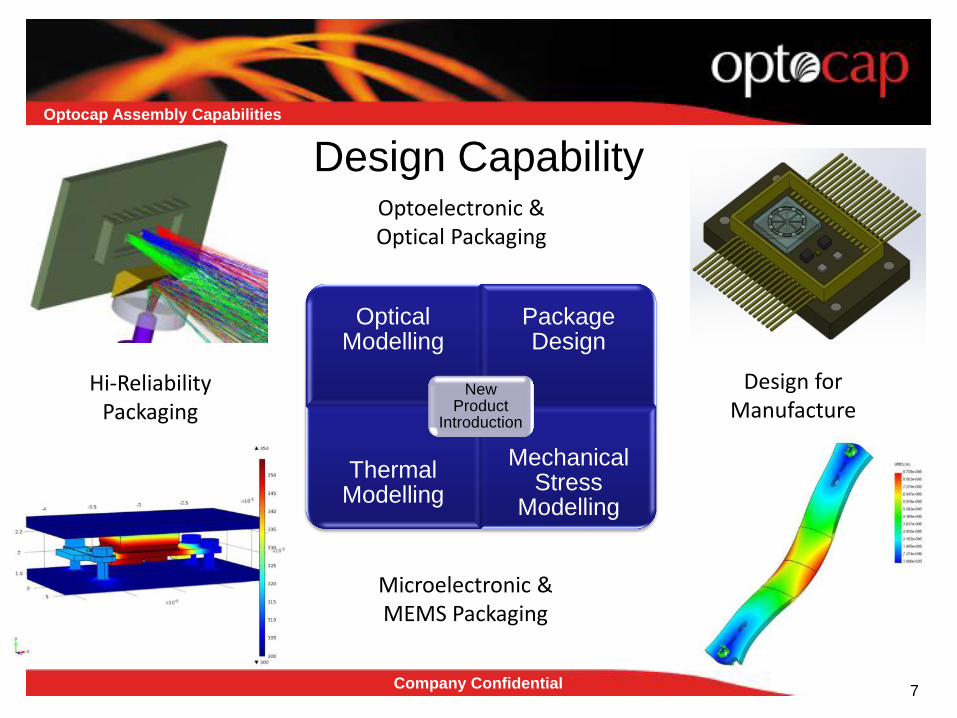
Design Capability
Optocap Assembly Capabilities
Optical Modelling
Package Design
Thermal Modelling
Mechanical Stress
Modelling
New Product
Introduction
Optoelectronic & Optical Packaging
Microelectronic & MEMS Packaging
Design for Manufacture
Hi-Reliability Packaging

Company Confidential
Assembly Capability
8
European
Production
Automated Pick & Place
Wafer Post Processing
Wire Bond
Flip Chip Ceramic &
Plastic Package
Hermetic Sealing
Optical Alignment
Optocap Assembly Capabilities
Company Confidential
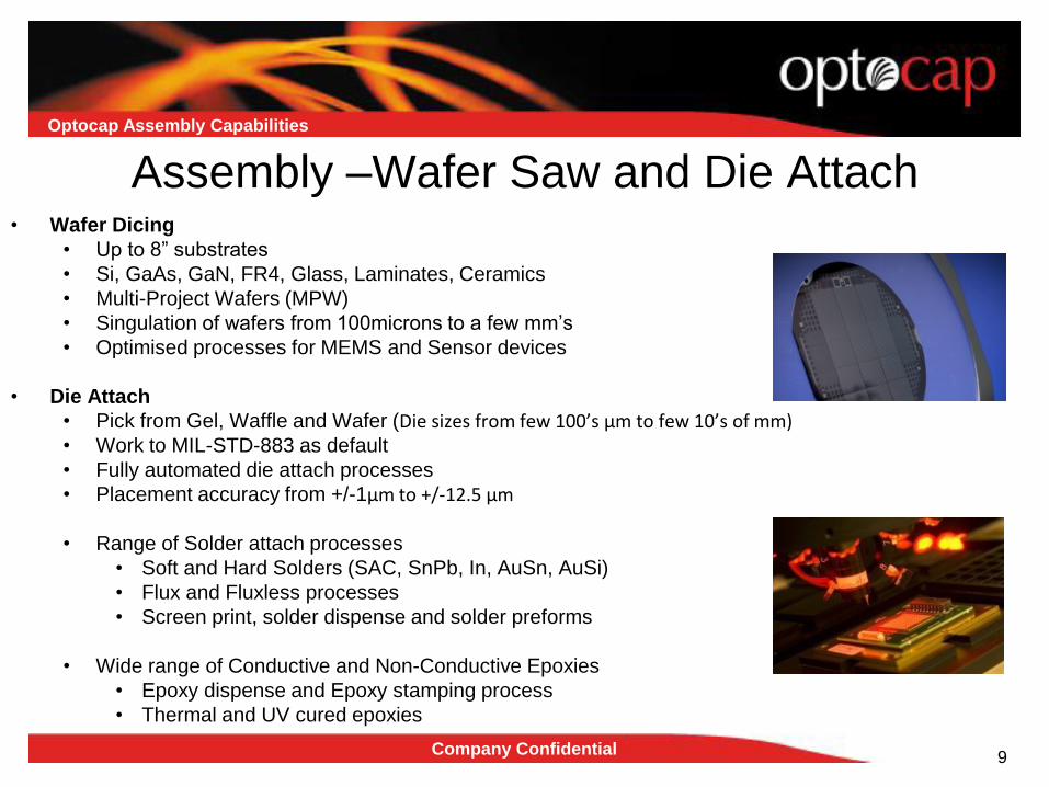
Assembly –Wafer Saw and Die Attach
9
• Wafer Dicing
• Up to 8” substrates
• Si, GaAs, GaN, FR4, Glass, Laminates, Ceramics
• Multi-Project Wafers (MPW)
• Singulation of wafers from 100microns to a few mm’s
• Optimised processes for MEMS and Sensor devices
• Die Attach
• Pick from Gel, Waffle and Wafer (Die sizes from few 100’s μm to few 10’s of mm) • Work to MIL-STD-883 as default
• Fully automated die attach processes
• Placement accuracy from +/-1μm to +/-12.5 μm
• Range of Solder attach processes
• Soft and Hard Solders (SAC, SnPb, In, AuSn, AuSi)
• Flux and Fluxless processes
• Screen print, solder dispense and solder preforms
• Wide range of Conductive and Non-Conductive Epoxies
• Epoxy dispense and Epoxy stamping process
• Thermal and UV cured epoxies
Optocap Assembly Capabilities

Company Confidential 10
Assembly – Wire Bonding
• Au Ball Bonding
• 17um to 33um Au wire diameter
• Wire bond down to 50um pitch
• Demonstrated 25um interleaved across 512 channel array
• Die to Die Bonding
• Reverse bonding
• Double sided Bonding
• Deep access wire bonding to 8mm
• Fully automated - 8 wire bonds per sec
• Wedge Bonding
• Au or Al wire
• Ribbon Bonding
• 75um x25um Au ribbon
Optocap Assembly Capabilities
ROIC

Company Confidential 11
Assembly – Wire Bonding
Optocap Assembly Capabilities
UHV MEMS Package Application
- ion-trap array, Quantum Field Experimentation
Company Confidential 12
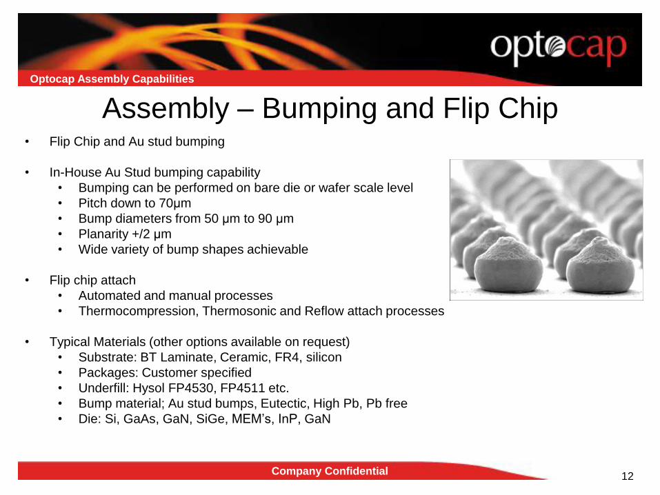
Assembly – Bumping and Flip Chip • Flip Chip and Au stud bumping
• In-House Au Stud bumping capability
• Bumping can be performed on bare die or wafer scale level
• Pitch down to 70μm
• Bump diameters from 50 μm to 90 μm
• Planarity +/2 μm
• Wide variety of bump shapes achievable
• Flip chip attach
• Automated and manual processes
• Thermocompression, Thermosonic and Reflow attach processes
• Typical Materials (other options available on request)
• Substrate: BT Laminate, Ceramic, FR4, silicon
• Packages: Customer specified
• Underfill: Hysol FP4530, FP4511 etc.
• Bump material; Au stud bumps, Eutectic, High Pb, Pb free
• Die: Si, GaAs, GaN, SiGe, MEM’s, InP, GaN
Optocap Assembly Capabilities

Company Confidential 13
Assembly – Encapsulation and Sealing
• Glob top and dam and fill
• Automated epoxy dispense systems
• Chip on Board Applications
• Seam seal, Solder seal and Projection Weld
• Ultra low moisture environments <1000ppm
• Specialist sealing environments He, N, Ar, O2
• Fine and Gross leak test to MIL-STD-883, (Space Flight Module Applications)
Optocap Assembly Capabilities
Company Confidential 14
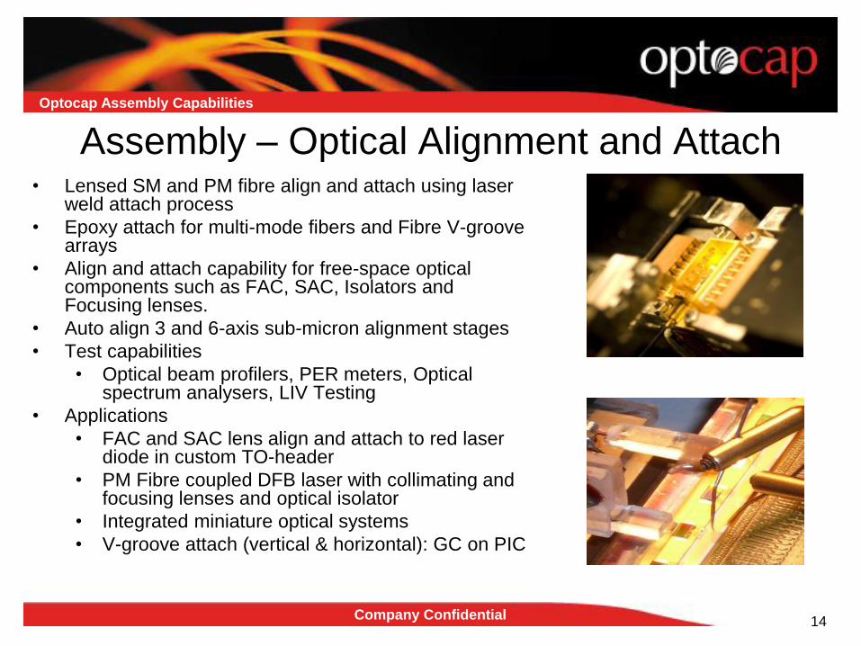
Assembly – Optical Alignment and Attach • Lensed SM and PM fibre align and attach using laser
weld attach process
• Epoxy attach for multi-mode fibers and Fibre V-groove arrays
• Align and attach capability for free-space optical components such as FAC, SAC, Isolators and Focusing lenses.
• Auto align 3 and 6-axis sub-micron alignment stages
• Test capabilities
• Optical beam profilers, PER meters, Optical spectrum analysers, LIV Testing
• Applications
• FAC and SAC lens align and attach to red laser diode in custom TO-header
• PM Fibre coupled DFB laser with collimating and focusing lenses and optical isolator
• Integrated miniature optical systems
• V-groove attach (vertical & horizontal): GC on PIC
Optocap Assembly Capabilities

Company Confidential 15
Assembly – Optical Alignment and Attach • Example of integrated sub-system (PD-PIC-ROIC )assembly development
• Technology development study to meet environmental and application requirements
Optocap Assembly Capabilities
(1) (2) (3)
(4)

Company Confidential
Embedded solution:
• Integrated SLED sub-module
• Improved optical coupling via
horizontal fibre v-groove to
grating coupler attach
Optocap Assembly Capabilities

Company Confidential
• Company History
- Markets and Services
• Design & Assembly Capabilities
• Case Study: Compound Semiconductor Photonic module
design & manufacture
17
Optocap Assembly Capabilities
Company Confidential
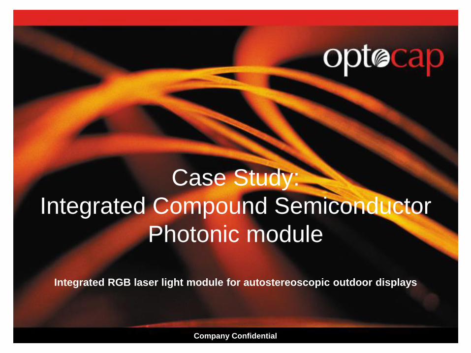
Case Study:
Integrated Compound Semiconductor
Photonic module
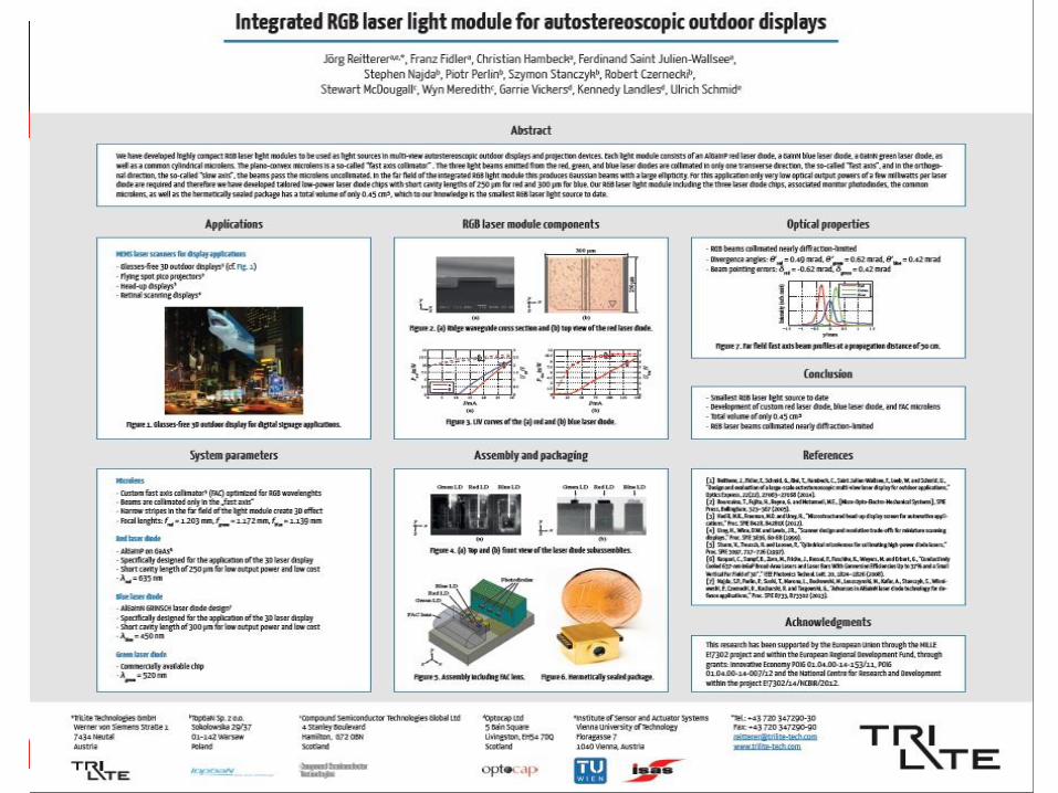
Integrated RGB laser light module for autostereoscopic outdoor displays

Company Confidential 19
Integrated CS Photonic sub system Case Study Integrated RGB laser light module for autostereoscopic outdoor displays
Case Study
• Integrated Optical & microelectronic sub assembly
• Custom design solution for pilot manufacture / proof of principle
• Hermetic Package / controlled internal environment
• Mechanical design:
- Outer package & sub assembly
- Process tooling and fixtures
• Optical & Thermal Design & Simulation study
• Process Development:
- LD placement
- FAC/SAC Active Alignment
World’s smallest RGB Laser Light Source (SPIE LASE 2015, San Francisco, CA,USA)
Company Confidential 20
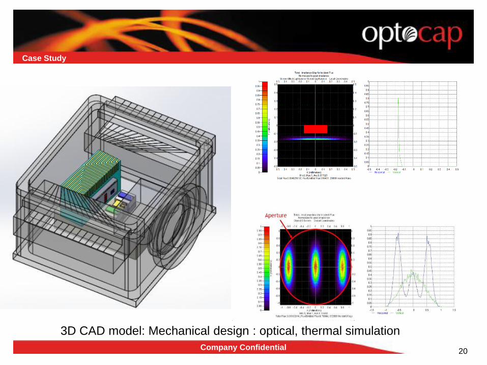
Case Study
3D CAD model: Mechanical design : optical, thermal simulation

Company Confidential 21
Case Study
LD flip-chip attach 3μm accuracy
Tolerances, Process / tool design

Company Confidential 22
Case Study
Active Alignment of lens
Probes Probe card
Optical Output

Company Confidential 23
Case Study
Company Confidential 24
Case Study
Company Confidential
THANK YOU
CONTACT:
EMAIL: [email protected]
WEBSITE: WWW.OPTOCAP.COM
TELEPHONE: +44 (0) 1506 403550
25
Optocap Assembly Capabilities


