NASA Technical Memorandum 107432 Army Research Laboratory Technical Report ARL-TR-1355 Microfabricated Ice-Detection Sensor Russell G. DeAnna U.S. Army Research Laboratory Lewis Research Center Cleveland, Ohio Mehran Mehregany and Shuvo Roy Case Western Reserve University Cleveland, Ohio Prepared for the Smart Structures and Materials Conference sponsored by the Society for Photo-Optical Instrumentation Engineers San Diego, California, March 2-6, 1997 National Aeronautics and Space Administration U.S. ARMY RESEARCH LABORATORY https://ntrs.nasa.gov/search.jsp?R=19970025167 2018-07-28T13:27:51+00:00Z
Transcript
NASA
Technical Memorandum 107432
Army Research Laboratory
Technical Report ARL-TR-1355
Microfabricated Ice-Detection Sensor
Russell G. DeAnna
U.S. Army Research Laboratory
Lewis Research Center
Cleveland, Ohio
Mehran Mehregany and Shuvo Roy
Case Western Reserve University
Cleveland, Ohio
Prepared for the
Smart Structures and Materials Conference
sponsored by the Society for Photo-Optical Instrumentation Engineers
Russell G. DeAnna a, Mehran Mehregany b, Shuvo Roy b, and Eugene Zakar c
a Vehicle Technology Center, US Army Research Laboratory, NASA Lewis Research
Center, Cleveland, OH 44135
b Microfabrication Laboratory, Department of Electrical Engineering & Applied Physics,
Case Western Reserve University, Cleveland, OH 44106
Sensors and Electron Devices Directorate, US Army Research Laboratory, Ft.
Monmouth, NJ, 07703
ABSTRACT
Knowledge of ice conditions on important aircraft lift and control surfaces is critical for safe operation.These conditions can be determined with conventional ice-detection sensors, but these sensors are
often expensive, require elaborate installation procedures, and interrupt the airflow. A micromachined,silicon-based, flush-mounted sensor which generates no internal heat has been designed, batchfabricated, packaged, and tested. The sensor is capable of distinguishing between an ice-covered anda clean surface. It employs a bulk micromachined wafer with a 7ktm-thick, boron-doped, silicon
diaphragm which serves as one plate of a parallel-plate capacitor. This is bonded to a second siliconwafer which contains the fixed electrodes -- one to drive the diaphragm by application of a voltage,
the other to measure the deflection by a change in capacitance. The diaphragm sizes ranged fromlxlmm to 3x3mm, and the gap between parallel-plate capacitors is 2_tm. A 200V d.c. was applied tothe driving electrode which caused the capacitance to increase approximately 0.6pf -- from a nominalcapacitance of 0.6pf -- when the surface was ice free. After the sensor was cooled below the freezingpoint of water, the same voltage range was applied to the drive electrode. The capacitance increasedby the same amount. Then a drop of water was placed over the diaphragm and allowed to freeze. Thiscreated an approximately 2mm-thick ice layer. The applied 200V d.c. produced no change incapacitance, confirming that the diaphragm was locked to the ice layer. Since the sensor usescapacitive actuation, it uses very little power and is an ideal candidate for inclusion in a wireless
Since the first aircraft flights during winter, icing has been recognized as a potentially dangerous
phenomenon. Numerous aircraft accidents have occurred due to icing, and ice detection must occurbefore ice removal. In the air, icing is caused by super-cooled water droplets in clouds, which are in ametastable condition. The droplets follow trajectories which will either strike the surface, or will be
carried away from it. When the aircraft encounters these droplets, they may either suddenly changephase upon impact, or may flow back as a thin film of water and collect into droplets due to surfacetension. The droplets may be swept off the surface by aerodynamic forces or freeze. The temperature
range normally associated with icing is from -40 to 0 C.
Various technologies have been used to detect ice. For a detailed account of these detectiontechniques and other icing-related issues consult the FAA handbook, l Microwave and other electro-mechanical techniques have been used for both point and area detection. 25 Vibrating probes anddiaphragms which change characteristics when ice covered have been used for point dection. 6'7
2. SENSOR DESIGN
A schematic, cross-sectional view of the ice-detection sensor is shown in Fig. 1. There are
two aluminum electrodes patterned on the Pyrex wafer and located under the diaphragm. The outsideelectrode is used to sense diaphragm deflection upon applied voltage to the drive, or inner, electrode.
i ii!iii i!iiPyrex glass _ boron etch stop aluminum
Figure 1: Sensor schematic cross section.
The capacitance and actuation voltages necessary to deflect the diaphragm depend stronglyon the distance between the diaphragm and electrodes, and also on the diaphragm area. A largerdiaphragm has a larger capacitance and requires a smaller actuation voltage, but is mechanically lessrobust and is also more sensitive to fluctuations in air pressure. Typical diaphragm dimensions arelmm by lmm square, 7p,m thick, suspended 2_m above the electrodes. These dimensions yield anominal capacitance of approximately 0.6pf between the diaphragm and either electrode. Theelectrodes have equal areas. The sensor is designed to operate with a 5 to 20V d.c. signal applied tothe drive electrode. This should yield a capacitance change of a fraction of a picofarad. See Fig. 2 fora plan view SEM picture of the electrodes.
Three contact pads are provided per die (though only the two which provide electricalconnections to the electrodes under the diaphragm can be seen in Fig. 2). The third contact padprovides electrical connection to the silicon substrate. The contact to the silicon substrate is throughan aluminum line that crosses over the shallow etch step in the glass wafer and is then sandwichedbetween the glass and silicon wafer. Since the surface of the silicon wafer is doped very heavily withboron, the aluminum contact to the silicon will be ohmic. Each contact pad has an area of250x250gm. The contact pads are exposed through windows etched in the silicon wafer.
NASA TM-107432 2
Figure 2: Plan view of aluminum electrodes.
Five diaphragm sizes - lxl, lx2, lx3, 2x2, and 3x3mm -- were included on the mask layout.For each diaphragm size, the area of the two concentric electrodes under the diaphragm was equal,and each electrode has approximately one-half the area of the diaphragm. Thus, the electrode area,
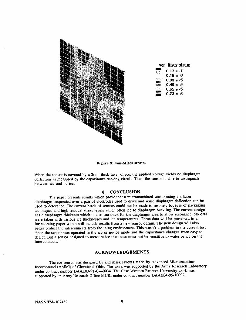
and not the diaphragm area, determines the electrode-to-diaphragm-capacitance magnitude. Twovariations in the positioning of the channel through which the connections to the electrodes under thediaphragm are made were included. This was done to investigate the change in deflection for eachtype since the maximum stress location for a rectangular diaphragm with fixed edges is at the middleof each side. (See Fig. 9 in the results section, which shows the von-Mises strain computed from theFEA.) In the case that the channel connects the diaphragm area with the bonding pad area through themiddle region of one of the diaphragm sides, the diaphragm mechanical response is expected todeviate more from the all-sides-fixed model than in the case when the channel is at the corner of oneof the sides.
The deflection of the diaphragm with applied voltage can be estimated by assuming the
diaphragm and electrodes form a pair of parallel-plate capacitors. The capacitance for such aconfiguration is given by
C=eA/x, (1)
where E is the dielectric of the material between the plates, A is the plate area, and x is the gap
between plates. For a lxlmm diaphragm suspended 2_m above the electrodes, in air, the nominalcapacitance is 0.6pf.* The capacitance change due to a change in gap spacing becomes
=- _-_-Ax. (AC 2)x _
This equation relates the capacitance change to diaphragm deflection, Ax. For a square plateclamped at the edges, the uniform pressure for a given maximum deflection is given by
p = -4.5E(L) 4 --Z_Xmax, (3)a t
which assumes no residual stress exists in the plate, s In this equation, t is the diaphragm thickness, a
is one-half the diaphragm edge lentgth, p is pressure, and E is Young's Modulus. Solving the above
equation for AXmax gives
tp a 4_aCmaX =-- 4--._(t) . (4)
For a voltage-driven plate, the pressure (load) is due to the applied voltage. For a parallel-platecapacitor the pressure for a given voltage is given by
t This assumes the drive and sense electrodes each occupy one-half the area of the diaphragm.
NASA TM-107432 3
Substituting this relation into the equation for maximum plate deflection gives
(5)
Et a 4 2- (T) v. ( 6)
This equation is used to verify the ANSYS FEA by comparing it with the center deflection computedby the model. For a square, silicon diaphragm in air of the dimensions given above, the centerdeflection becomes
Axm_ = 2.8x10 -I° V 2(m). (7)
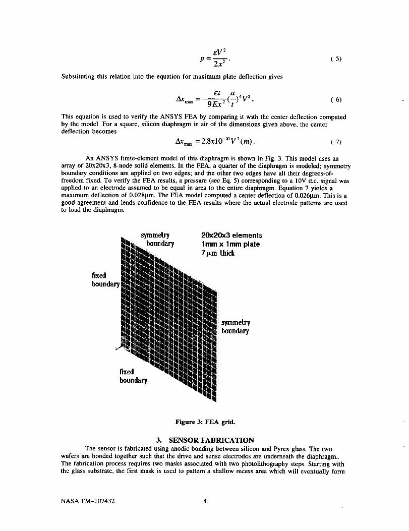
An ANSYS finite-element model of this diaphragm is shown in Fig. 3. This model uses anarray of 20x20x3, 8-node solid elements. In the FEA, a quarter of the diaphragm is modeled; symmetryboundary conditions are applied on two edges; and the other two edges have all their degrees-of-freedom fixed. To verify the FEA results, a pressure (see Eq. 5) corresponding to a 10V d.c. signal wasapplied to an electrode assumed to be equal in area to the entire diaphragm. Equation 7 yields amaximum deflection of 0.028_tm. The FEA model computed a center deflection of 0.026_tm. This is agood agreement and lends confidence to the FEA results where the actual electrode patterns are usedto load the diaphragm.
20x20x3 elements
lmm x lmm plate7Fro thick
fixed
boundary
symmetry
boundary
fixed
boundary
Figure 3: FEA grid.
3. SENSOR FABRICATION
The sensor is fabricated using anodic bonding between silicon and Pyrex glass. The twowafers are bonded together such that the drive and sense electrodes are underneath the diaphragm..The fabrication process requires two masks associated with two photolithography steps. Starting withthe glass substrate, the first mask is used to pattern a shallow recess area which will eventually form
NASA TM-107432 4
the air gap between diaphragm and substrate and the access passages for aluminum interconnections.Standard (positive resist) lithography and an HF-based solution are used to create the recessed areas.Next, aluminum is deposited on the glass substrate by sputtering. The aluminum film is approximately0.31xm thick. The aluminum is patterned with the second mask, using standard lithography and a wetaluminum etch.
The starting silicon wafer is oxidized thermally to grow a 1 I.tm-thick layer. The startingsilicon wafer is (100), moderately doped n-type, double-sided polished, with a <100> major flat.Oxide on one surface is protected with hard-baked photoresist and the oxide on the opposite surface isremoved in buffered HF. Next, the wafer is diffused with boron to create a boron etch stop layer, onthe side with no oxide, with a thickness around 7_tm. The boron-doped glass is removed in buffered
HF.
The silicon wafer is electrostatically bonded to the glass wafer. The bonding step only
requires good global alignment of the two wafers. The wafers are then etched in KOH, leaving behindthe boron etch stop. The metal pads are sealed by the boron etch stop membrane. The pads are
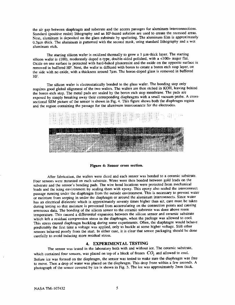
exposed by simply breaking away their corresponding diaphragms with a small vacuum probe. A cross-sectional SEM picture of the sensor is shown in Fig. 4. This figure shows both the diaphragm regionand the region containing the passage for the aluminum interconnects for the electrodes.
! !ii i !iil !!!i!! ! iii!il/ii!i!i!iil i!i!ii!ili!i!.... ii iiii¸¸
_ _:!_i_,::_ i ,.
Figure 4: Sensor cross section.
After fabrication, the wafers were diced and each sensor was bonded to a ceramic substrate.Four sensors were mounted on each substrate. Wires were then bonded between gold leads on the
substrate and the sensor's bonding pads. The wire bond locations were protected from mechanicalloads and the icing environment by sealing them with epoxy. This epoxy also sealed the interconnectpassage running under the diaphragm from the outside environment. This is necessary to prevent wateror moisture from seeping in under the diaphragm or around the aluminum interconnects. Since waterhas an electrical dielectric which is approximately seventy times higher than air, care must be taken
during testing so that moisture is prevented from accumulating on the connection points and causingerroneous data. The bonding of the silicon sensor to the ceramic substrate was done above room
temperature. This caused a differential expansion between the silicon sensor and ceramic substratewhich left a residual compression stress in the diaphragm, when the package was allowed to cool.This stress caused diaphragm buckling during some experiments. Often, the diaphragm would behave
predictably the first time a voltage was applied, only to buckle at some higher voltage. Still othersensors behaved poorly from the start. In either case, it is clear that sensor packaging should be done
carefully to avoid inducing more residual stress.
4. EXPERIMENTAL TESTING
The sensor was tested in the laboratory both with and without ice. The ceramic substrate,
which contained four sensors, was placed on top of a block of frozen CO 2 and allowed to cool.
Before ice was formed on the diaphragm, the sensor was tested to make sure the diaphragm was freeto move. Then a drop of water was placed on the diaphragm. This drop froze within a few seconds. A
photograph of the sensor covered by ice is shown in Fig. 5. The ice was approximately 2mm thick.
NASA TM-107432 5
Figure 5: Ice-covered sensor.
A d.c. voltage was applied to the drive electrode through a large-magnitude resistor -typically 100 K ohms. The sense electrode was connected to the input of a frequency-modulated (FM)oscillator circuit which was used to measure the capacitance change. The FM oscillator has anominal carrier frequency of 48MHz. The unit contains the FM oscillator, electronics and a signalconditioner. The signal conditioner demodulates the oscillator output. Capacitance change isregistered as a change in the frequency of the demodulator. The oscillator frequency increases withincreasing capacitance between diaphragm and sense electrode. See Fig. 6 for a circuit diagram.
where C Ois the nominal circuit capacitance and C b (v) is the capacitance of the sensor. An important
aspect of FM-oscillator design is the frequency of oscillation. The oscillating frequency without
applied voltage, that is, when C(O) = C O + C b (0), is defined as the carrier frequency f_, or
1 Illlf_ = "2"_'_'_/LC(O)' ( 9 )
where Lis the inductance of the inductor in the oscillator. The nominal frequency with zero applied
voltage, fc, is used to compute the nominal value of LC(O). The nominal capacitance, Cb(0),
must be measured separately. The applied voltage causes a small change in the carder frequency,
defined as the frequency deviation Arc, found from
Arc = -[Cb(V) --Cb(O)] 4_(0) C7(0) (10)
Rearranging gives the capacitance change as
Cb (v) - Cb(O ) = 4_AfcC(0),_--_, (11)
which expresses the basic relationship between the capacitance change, as reflected in Cb(v) and
the quantities Afc, L, and C(0). These quantities can then be used to compute the capacitance
change for any applied voltage.
5. RESULTS
All of the experimental and theoretical results apply to a sensor with a diaphragm of lxlmm
area, 71.tm -thick, suspended 2_m above the electrodes. Results were obtained both with and withoutice. No attempt was made to detect ice thickness, and the goal was to yield either an ice or no-ice
signal. No data were obtained with other ice thicknesses or temperatures.1.2.
t_
t.)
De Voltage (volts)
Figure 7: Capacitance change versus voltage.
NASA TM-107432 7
Figure7 showscapacitancechangeversus applied voltage for the experiment both with andwithout ice and for the ANSYS FEA without ice. In the FEA model a pressure, corresponding to agiven voltage according to Eq. 5, was applied to the model over an area corresponding to the driveelectrode (a 0.5x0.5mm area at the center of the diaphragm). The figure applies to a diaphragmwithout ice. There was no measurable difference in capacitance change between a room-temperatureand cooled sensor when there was no ice covering the diaphragm. In the experiment, the capacitancechange was measured directly by the signal-processing circuit; the capacitance change for the FEAwas computed by numerically integrating the equation for capacitance change (Eq. 2) over the arearepresented by the sense electrode, i.e., that area outside of the 0.5x0.5mm area representing the driveelectrode. The experimental capacitance change was approximately 60% less than the FEA. Thisdifference is expected since the FEA doesn't consider residual stress or buckling. The maximumdeflection from the FEA is 0.0641am. Figure 9 shows the computed von-Mises strain. It showsmaximum strain at the center of each edge and minimum strain at the comers.
plate deflection m}
m 0.064
ii_:.i!_;i._i_0.047
::: 0.0210.007
::L;:': 0.000III
Figure 8: Diaphragm deflection.
NASA TM-107432 8
yon Mises strain
ii 0.17 e -7
0.16 e -6_:: 0.3:3 e-5
_;_,_,_ 0.49 e -5ii=_=::_:0.65 e -5
_ 0.73 e -5
Figure 9: von-Mises strain.
When the sensor is covered by a 2mm-thick layer of ice, the applied voltage yields no diaphragmdeflection as measured by the capacitance sensing circuit. Thus, the sensor is able to distinguishbetween ice and no ice.
6. CONCLUSION
The paper presents results which prove that a micromachined sensor using a silicondiaphragm suspended over a pair of electrodes used to drive and sense diaphragm deflection can beused to detect ice. The current batch of sensors could not be made to resonate because of packaging
techniques and high residual stress levels which often led to diaphragm buckling. The current designhas a diaphragm thickness which is also too thick for the diaphragm area to allow resonance. No datawere taken with various ice thicknesses and ice temperatures. These data will be presented in aforthcoming paper which will include results from a new sensor design. The new design will alsobetter protect the interconnects from the icing environment. This wasn't a problem in the current testsince the sensor was operated in the ice or no-ice mode and the capacitance changes were easy todetect. But a sensor designed to measure ice thickness must not be sensitive to water or ice on theinterconnects.
ACKNOWLEDGEMENTS
The ice sensor was designed by and mask layouts made by Advanced Micromachines
Incorporated (AMMi) of Cleveland, Ohio. The work was supported by the Army Research Laboratoryunder contract number DAAL03-91-C---4)034. The Case Western Reserve University work was
supported by an Army Research Office MURI under contract number DAAH04-95-10097.
NASA TM-107432 9
1.
.
3.
4.
.
6.
7.
REFERENCES
Heinrich, A., et al., Aircraft Icing Handbook, Technical Center Publication DOT/FAA/CT-88/8-2,FAA, 1991.
Gerardi, J. J. and G. A. Hickman, "Distributed ice accretion sensor for smart aircraft structures,"
Hansman, R. J.and M. S. Kirby, "Measurement of ice accretion using ultrasonic pulse-echotechniques," 23 _ AIAA Aerospace Sciences Meeting, Reno, NV, Jan. 14-17, 1985.
Magenheim, B. and J. K. Bocks, "Microwave ice accretion measurement instrument," 20 m mImmAerospace Sciences Meeting, Orlando, FL, Jan. 11-14, 1982.
Jensen, D. P. And D. J. Moore, "An ice detection and control system for fixed and rotary wingaircraft," 8 th Annual National Conference on Environmental Effects on Aircraft and Propulsion
Systems, Bordentown, NJ, Oct. 8-10, 1968.
Lustenberger, M. "New ice detection system," Proceedings of the 14 th Symposium on AircraftIntegrated Monitoring Systems, p. 619-638, Vibrometer, Fribourg, Switzerland, 1988.
8. Timoshenko, S., et al, Theol. of Plates and Shells, p. 202, McGraw Hill, New York, 1959.
NASA TM-107432 10
Form Approved
REPORT DOCUMENTATION PAGE OMa No. 0704-0188
Public reporting burden for this collection of information is estimated to average 1 hour per response, including the time for reviewing instructions, searching existing data sources,
gathering and maintaining the data needed, and completing and reviewing the collection of information, Send comments regarding this burden estimate or any other aspect of this
collection of information, including suggestions for reducing this burden, to Washington Headquarters Services, Directorate for information Operations and Reports, 1215 Jefferson
Davis Highway, Suite 1204, Arlington, VA 22202-4302, end to the Office of Management and Budget, Paperwork Reduction Project (0704-0188), Washington, DC 20503,
1. AGENCY USE ONLY (Leave blank) 2. REPORT DATE 3. REPORT TYPE AND DATES COVERED
June 1997 Technical Memorandum
5. FUNDING NUMBERS4. TITLE AND SUBTITLE
Microfabricated Ice-Detection Sensor
6. AUTHOR(S)
Russell G. DeAnna, Mehran Mehregany, and Shuvo Roy
7. PERFORMING ORGANIZATION NAME(S) AND ADDRESS(ES)
NASA Lewis Research Center
Cleveland. Ohio 44135-3191
and
U.S. Army Research Laboratory
Cleveland, Ohio 44135-3191
9. SPONSORING/MONITORING AGENCY NAME(S) AND ADDRESS(ES)
Nadonal Aeronautics and Space Administration
Washington, DC 20546-0001and
U.S. Army Research Laboratory
Adelphi, Maryland 20783-1145
WU-523-26-13
1L161102AH45
8. PERFORMING ORGANIZATIONREPORT NUMBER
E-10690
10. SPONSORING/MONITORING
AGENCY REPORT NUMBER
NASA TM-107432
ARL-TR-1355
11. SUPPLEMENTARY NOTES
Prepared for the Smart Structures and Materials Conference sponsored by the Society for Photo-Optical Instrumentation Engineers, San
Deigo, California, March 2_, 1997. Russell G. DeAnna, U.S. Army Research Laboratory, NASA Lewis Research Center; Mehran
Mehregany and Shuvo Roy, Case Western Reserve University, Cleveland, Ohio 44106. Responsible Person, Russell G. DeAnna, organization