research papers 1462 http://dx.doi.org/10.1107/S1600577516014788 J. Synchrotron Rad. (2016). 23, 1462–1473 Received 16 June 2016 Accepted 19 September 2016 Edited by M. Yamamoto, RIKEN SPring-8 Center, Japan ‡ These authors contributed equally to this work. Keywords: hybrid detectors; silicon detectors; interpolation; grating interferometry. Micrometer-resolution imaging using MO ¨ NCH: towards G 2 -less grating interferometry Sebastian Cartier, a ‡ Matias Kagias, a,b ‡ Anna Bergamaschi, a * Zhentian Wang, a,b Roberto Dinapoli, a Aldo Mozzanica, a Marco Ramilli, a Bernd Schmitt, a Martin Bru ¨ckner, a Erik Fro ¨jdh, a Dominic Greiffenberg, a Davit Mayilyan, a Davide Mezza, a Sophie Redford, a Christian Ruder, a LukasScha¨dler, a Xintian Shi, a Dhanya Thattil, a Gemma Tinti, a Jiaguo Zhang a and Marco Stampanoni a,b a Paul Scherrer Institute, 5232 Villigen PSI, Switzerland, and b Institute for Biomedical Engineering, University and ETH Zurich, 8092 Zurich, Switzerland. *Correspondence e-mail: [email protected]MO ¨ NCH is a 25 mm-pitch charge-integrating detector aimed at exploring the limits of current hybrid silicon detector technology. The small pixel size makes it ideal for high-resolution imaging. With an electronic noise of about 110 eV r.m.s., it opens new perspectives for many synchrotron applications where currently the detector is the limiting factor, e.g. inelastic X-ray scattering, Laue diffraction and soft X-ray or high-resolution color imaging. Due to the small pixel pitch, the charge cloud generated by absorbed X-rays is shared between neighboring pixels for most of the photons. Therefore, at low photon fluxes, interpolation algorithms can be applied to determine the absorption position of each photon with a resolution of the order of 1 mm. In this work, the characterization results of one of the MO ¨ NCH prototypes are presented under low-flux conditions. A custom interpolation algorithm is described and applied to the data to obtain high-resolution images. Images obtained in grating interferometry experiments without the use of the absorption grating G 2 are shown and discussed. Perspectives for the future developments of the MO ¨ NCH detector are also presented. 1. Introduction Hybrid pixel detectors are widely used in X-ray applications as they are able to fulfill most of the requirements of the experiments: single-photon sensitivity, large dynamic range, wide area coverage, fast frame rate, simple, stable and user- friendly operation. Photon-counting detectors are well established at synchro- trons, e.g. PILATUS (Kraft et al., 2009), EIGER (Dinapoli et al., 2011), MEDIPIX (Gimenez et al., 2015), IMXPAD (Medjoubi et al., 2012). However, due to the pulsed structure of the beam, they are unusable at X-ray free-electron lasers (XFELs). In the last few years, this boosted the development of charge-integrating hybrid detectors like CSPAD (Herr- mann et al., 2014), GOTTHARD (Mozzanica et al., 2012), AGIPD (Greiffenberg, 2012), DSSC (Porro et al. , 2012), LPD (Koch et al., 2013), JUNGFRAU (Mozzanica et al., 2014). These detectors can offer the same data quality as photon- counting detectors (Henrich et al., 2011), while overcoming some of their disadvantages, including the minimum detect- able energy, the saturation at high count rates and the limits on the pixel size due to charge sharing (Bergamaschi et al., 2014). However, hybrid detectors have never been considered as candidates for soft X-ray detection due to their relatively large electronic noise [a few hundreds eV r.m.s. compared with a ISSN 1600-5775
Transcript
research papers
1462 http://dx.doi.org/10.1107/S1600577516014788 J. Synchrotron Rad. (2016). 23, 1462–1473
Received 16 June 2016
Accepted 19 September 2016
Edited by M. Yamamoto, RIKEN SPring-8
Center, Japan
‡ These authors contributed equally to this
work.
Keywords: hybrid detectors; silicon detectors;
interpolation; grating interferometry.
Micrometer-resolution imaging using MONCH:towards G2-less grating interferometry
Sebastian Cartier,a‡ Matias Kagias,a,b‡ Anna Bergamaschi,a* Zhentian Wang,a,b
Roberto Dinapoli,a Aldo Mozzanica,a Marco Ramilli,a Bernd Schmitt,a
Martin Bruckner,a Erik Frojdh,a Dominic Greiffenberg,a Davit Mayilyan,a
Davide Mezza,a Sophie Redford,a Christian Ruder,a Lukas Schadler,a Xintian Shi,a
Dhanya Thattil,a Gemma Tinti,a Jiaguo Zhanga and Marco Stampanonia,b
aPaul Scherrer Institute, 5232 Villigen PSI, Switzerland, and bInstitute for Biomedical Engineering,
University and ETH Zurich, 8092 Zurich, Switzerland. *Correspondence e-mail: [email protected]
MONCH is a 25 mm-pitch charge-integrating detector aimed at exploring the
limits of current hybrid silicon detector technology. The small pixel size makes
it ideal for high-resolution imaging. With an electronic noise of about 110 eV
r.m.s., it opens new perspectives for many synchrotron applications where
currently the detector is the limiting factor, e.g. inelastic X-ray scattering, Laue
diffraction and soft X-ray or high-resolution color imaging. Due to the small
pixel pitch, the charge cloud generated by absorbed X-rays is shared between
neighboring pixels for most of the photons. Therefore, at low photon fluxes,
interpolation algorithms can be applied to determine the absorption position
of each photon with a resolution of the order of 1 mm. In this work, the
characterization results of one of the MONCH prototypes are presented under
low-flux conditions. A custom interpolation algorithm is described and applied
to the data to obtain high-resolution images. Images obtained in grating
interferometry experiments without the use of the absorption grating G2 are
shown and discussed. Perspectives for the future developments of the MONCH
detector are also presented.
1. Introduction
Hybrid pixel detectors are widely used in X-ray applications
as they are able to fulfill most of the requirements of the
experiments: single-photon sensitivity, large dynamic range,
wide area coverage, fast frame rate, simple, stable and user-
friendly operation.
Photon-counting detectors are well established at synchro-
trons, e.g. PILATUS (Kraft et al., 2009), EIGER (Dinapoli
et al., 2011), MEDIPIX (Gimenez et al., 2015), IMXPAD
(Medjoubi et al., 2012). However, due to the pulsed structure
of the beam, they are unusable at X-ray free-electron lasers
(XFELs). In the last few years, this boosted the development
of charge-integrating hybrid detectors like CSPAD (Herr-
mann et al., 2014), GOTTHARD (Mozzanica et al., 2012),
AGIPD (Greiffenberg, 2012), DSSC (Porro et al., 2012), LPD
(Koch et al., 2013), JUNGFRAU (Mozzanica et al., 2014).
These detectors can offer the same data quality as photon-
counting detectors (Henrich et al., 2011), while overcoming
some of their disadvantages, including the minimum detect-
able energy, the saturation at high count rates and the limits on
the pixel size due to charge sharing (Bergamaschi et al., 2014).
However, hybrid detectors have never been considered as
candidates for soft X-ray detection due to their relatively large
electronic noise [a few hundreds eV r.m.s. compared with a
stability and difficulties in fabricating large-area gratings for
hard X-rays (Roessl et al., 2014).
The micrometer-level resolution delivered by the MONCH
detector after interpolation allows the interference fringes to
be resolved without the use of G2. The phase shift introduced
by the sample can be retrieved from the MONCH data by
combining position interpolation algorithms with an algorithm
based on a Hilbert transform optimized to compensate for the
position-dependent spatial resolution of the detector.
In this work, x2 describes the MONCH detector system and
the MONCH0.2 prototype. x3 shows the characterization
measurements. The data analysis and algorithms for position
interpolation of single photons are explained in detail and
applied to the imaging of a biological sample in x4. In x5 the
proof of principle of a G2-less grating interferometry experi-
ment is demonstrated. Finally, the results are discussed and
perspectives for future optimization are given.
2. MONCH detector description
2.1. The MONCH hybrid detector
MONCH is a charge-integrating hybrid pixel detector
project with a small pixel pitch of 25 mm currently developed
at the Paul Scherrer Institut (PSI, Switzerland) (Dinapoli et
al., 2014). The sensor consists of a 320 mm-thick n-doped high-
resistivity silicon wafer. The n+-doped back-plane is kept at a
stable high-bias voltage of 90–120 V, while the 25 mm-pitch
p+-doped electrodes are connected to the readout electronics
by means of indium bumps of size a few micrometers (Lutz,
1999).
The X-rays are absorbed in the silicon sensor producing
electron–hole pairs (Q0 = E0 /3.62 eV in silicon, where E0 is the
photon energy and Q0 is the number of electron–hole pairs
generated). Due to the high electric field applied to the fully
depleted silicon wafer, the electrons drift towards the back-
plane, while the holes are collected by the p+ implants and are
then integrated in parallel and fully independently by each
single pixel in the Application Specific Integrated Circuit
(ASIC), which is read out over several serial analog lines and
finally digitized by external commercial analog-to-digital
converters (ADCs).
While drifting to the collecting electrodes, the charge cloud
diffuses and can be collected by several pixels, depending on
the absorption position. This effect is known as charge sharing
and is more prominent in smaller pixel pitch detectors. The
amount of charge sharing depends on several parameters
including the sensor thickness, the sensor bias and the photon
energy (Cartier et al., 2014, 2015). It has been measured that,
for a 320 mm-thick silicon sensor biased with 120 V, the size of
the charge cloud is of the order of 17� 3 mm in the 10–20 keV
energy range (Bergamaschi et al., 2008).
The 25 mm pixel pitch has been chosen as a trade-off
between opposite constraints. On the one hand the pitch has
to be small enough such that the charge produced by the
majority of the photons will be shared between neighboring
pixels to be able to effectively perform interpolation. On the
other hand, small pixel sizes are very challenging both in terms
of bump-bonding yield, due to the small size and increasing
force to be applied, and in terms of electronics design due to
the constraints in the pixel area and power consumption.
research papers
J. Synchrotron Rad. (2016). 23, 1462–1473 Sebastian Cartier et al. � Micrometer-resolution imaging using MONCH 1463
ASIC and sensor design as well as bump-bonding are
performed in-house by the Swiss Light Source (SLS) Detector
group.
In this commissioning phase, the same readout board as
developed for the GOTTHARD microstrip detector has been
used for data acquisition (Mozzanica et al., 2012), with some
adaptation of the firmware and software to match the
requirements of the MONCH pixel detector. With a 1 Gb s�1
data transfer interface, it allows a maximum frame rate
of 1 kHz.
2.2. The MONCH readout chip
Several prototype ASICs were designed in UMC 110 nm
technology. Details can be found in the paper by Dinapoli et
al. (2014). The data presented in this work have been acquired
using the MONCH0.2 prototype. It is a fully functional small-
scale ASIC of 4 mm� 4 mm, containing an array of 160� 160
pixels. This array is subdivided into five blocks, each featuring
a different pixel architecture. Two blocks have statically
selectable preamplifier gains and target synchrotron applica-
tions. In low-gain mode they still provide single-photon
sensitivity for energies higher than 6 keV as well as a
reasonable dynamic range for such a small area (>120 12 keV
photons). In high gain, they target high-resolution low-flux
experiments where charge sharing can be exploited to reach
micrometer-level resolution. Three other architectures
address possible uses at XFELs and implement automatic
switching between two gains to increase the dynamic range, as
well as input overvoltage control.
The dynamic range of charge-integrating detectors scales
with the available area for the integration capacitance in the
pixel. Therefore compared with a larger pixel pitch of 75 mm
(e.g. JUNGFRAU) the dynamic range per pixel is reduced by
about a factor of nine, but remains constant per unit of area,
allowing the same total flux to be measured.
The basic pixel structure, common to all sub-blocks, is
shown in Fig. 1. The charge produced in the sensor by the
impinging photons is integrated by the feedback capacitor of
the charge amplifier. Two different capacitors can be switched
into the feedback loop to obtain two different preamp gains. A
correlated double sampling (CDS) stage follows, to reduce the
low-frequency noise contributions coming from the preamp
and its reset transistor (Buttler et al., 1990). The output of the
CDS is stored locally on a capacitor, which gives the pixel the
ability to be continuously sensitive: after storage the pre-
amplifier and CDS are available again for processing the next
image, while the readout of the current image can happen
simultaneously. The gain of the CDS buffer can be statically
selected between 4 (for low-noise applications) and 0.5 (to
extend the dynamic range).
The voltage stored on the storage capacitor is driven to the
chip periphery by an off-pixel buffer and is refreshed by a
column buffer. The signal produced by every column buffer is
serially multiplexed to a common single-ended-to-differential
off-chip buffer (not shown in the figure).
All the results shown in this paper are obtained using a
single sub-block of 40 � 160 pixels (1 mm � 4 mm) of
MONCH0.2 optimized for single-photon sensitivity by using
the high preamplifier gain and a CDS gain of 4. The same pixel
architecture was also selected for the design of MONCH0.3, a
10 mm � 10 mm (400 � 400 pixels) chip, which is at present
undergoing test and characterization.
2.3. Cluster finding
Due to charge sharing, a single pixel only partially collects
the charge generated by a photon. Therefore, the summation
of the charge from the cluster of channels among which it is
shared (clustering) is required to retrieve the correct radiation
spectrum. To analyze single-photon absorption events which
are shared between neighboring pixels, a cluster finding
algorithm (CFA) has been developed, as described by Cartier
et al. (2014). The CFA is effective only on datasets with low
occupancy, i.e. with on average less than one photon per 3 � 3
pixel cluster (single-photon regime). It considers as photons
only the events where either the total signal collected by a
cluster or the signal of a single pixel exceed the electronic
noise by five times its electron noise charge (ENC), defined as
the signal at the input of the electronic chain which would
result in the measured noise (Radeka, 1988). The pixel
pedestal and the electronic noise threshold are continuously
tracked during the acquisition to compensate for drifts
induced in the dark image signal and noise properties of each
pixel by temperature and other environmental changes.
Additional constraints for adjacent pixels are applied to
ensure that only one cluster is extracted
per photon hit and overlaps of clusters
from more than one photon are
discarded. A good signal-to-noise ratio
(SNR) is crucial in order to detect also
the photons for which the charge is
shared and collected by several pixels
in the cluster.
Fig. 2 shows the spectrum of 16 keV
monochromatic radiation for a single
pixel and for 2 � 2 and 3 � 3 pixels.
While a single pixel carries only limited
information concerning the X-ray
energy, the full charge is already
research papers
1464 Sebastian Cartier et al. � Micrometer-resolution imaging using MONCH J. Synchrotron Rad. (2016). 23, 1462–1473
Figure 1Simplified diagram of the basic pixel architecture of MONCH.
retrieved by a 2 � 2 pixel cluster, despite the increase in noise
by a factor of two due to summation.
x4 explains in detail how it is possible to improve the image
resolution beyond the pixel size by analyzing the charge ratio
between the individual pixels of each cluster. The final reso-
lution depends not only on the amount of charge sharing but
also on the SNR, hence the effort on limiting the electronic
noise in the MONCH ASIC.
3. MONCH characterization
The MONCH0.2 ASIC bump-bonded in-house to 160 � 160
25 mm-pitch pixels, 320 mm-thick silicon sensor produced by
HAMAMATSU, has been thoroughly characterized. Here we
report the major achievements regarding the first super-
column of the ASIC operated in the single-photon regime
which has been used for the imaging experiments shown in
xx4 and 5
3.1. Bump-bond yield
Given the small pixel pitch, the feasibility of the bump-
bonding technique developed and applied in-house at PSI had
to be demonstrated. The process required only minor modi-
fications compared with the one used for large pixels (e.g.
PILATUS 172 mm, EIGER 75 mm). The size of the under-
bump-metallization and indium bumps have been adapted to
the 25 mm pitch for the processing of the ASIC and of the
sensor wafers. The pressure applied during the bump-bonding
procedure also had to be rescaled to compensate for the much
higher pixel density.
Fig. 3(a) shows an image of a flat-field and Fig. 3(b)
represents the count distribution acquired in the single-photon
regime at 16.7 keV at the TOMCAT beamline of the SLS after
applying the CFA for the first supercolumn of the detector
assembly used for the measurements in this paper. The border
pixels have been excluded from the analysis because clusters
are lost along the edges.
The photon distribution is uniform over the whole detector
taking into account the variations of the illuminating beam
and the gain differences between pixels. Only the two pixels
with too few counts can be attributed to faulty bump-bonding,
resulting in a bump-bond yield of better than 99.95%.
Comparable results have been obtained also on the other
detectors assembled. During the development phase, the main
issues came from the processing of the single ASIC dice since
full wafers cannot be purchased in the prototyping phase. The
bump-bond yield is close to this level also for the larger
1 cm � 1 cm (400 � 400 pixels) MONCH0.3 detector.
The outstanding bump-bonding yield is a very important
achievement in the development of small pitch pixel detectors
and it is particularly crucial in the case of high-resolution
imaging applications using interpolation. In fact a non-bump-
bonded pixel affects also the charge collection in its neighbors
and therefore prevents the use of the full 3� 3 pixel cluster for
interpolation. Moreover these nine pixels correspond to a
much larger number of virtual pixels in the high-resolution
rebinned image obtained after interpolation.
3.2. Gain calibration
In order to extract the gain G necessary to convert the
signal pulse height (in mV or ADC units) into energy or
charge (Q = E/3.6 eV), flat-field spectra at different energies
need to be acquired. This calibration is necessary to correctly
compare the signal collected by neighboring pixels when
applying the CFA or performing interpolation (see x4).
Hereafter, the simplified linear model of charge sharing
in small pitch pixel sensors described by Bergamaschi et al.
(2015) has been used to describe the charge collection of
research papers
J. Synchrotron Rad. (2016). 23, 1462–1473 Sebastian Cartier et al. � Micrometer-resolution imaging using MONCH 1465
Figure 3(a) Flat-field image and (b) count distribution of the first supercolumn ofMONCH0.2. Only two of the 4470 pixels plotted count too few photonsand can be attributed to faulty bump-bonding. The estimated bump-bondyield is better than 99.95%.
Figure 2Spectrum of a single pixel [fitted using equation (1)], 2� 2 pixel and 3� 3pixel clusters (fitted with a Gaussian) acquired at 16 keV.
single pixels. The spectra S acquired for each pixel have been
fitted with the function
S Eð Þ ¼ N0
(A
�ffiffiffiffiffiffi2�p exp �
ðE� E0Þ2
2�2
� �
þ B� C lnE
E0
� �� �1� Erf ðE� E0Þ=�
� �2E0
); ð1Þ
where E is the signal amplitude and the fit parameters are E0
representing the X-ray energy, � the electronic noise and N0
the number of photons. A, B, C are proportional to the area
where no charge sharing is observed; charge sharing occurs
between two pixels (edges) and between four pixels (corners).
They can be written as a function of the average size � of the
charge cloud after drift and diffusion,
A ¼1� �ð Þ
2
1þ �ð Þ2; B ¼ 4
� 1� �ð Þ
1þ �ð Þ2; C ¼ 4
�2
1þ �ð Þ2: ð2Þ
For each pixel, G can be extracted as the angular coefficient
of the straight line correlating the X-ray energies with the
parameters E0 in mV or ADC units.
An average value of G = 102.6 � 2.9 ADC keV�1 has been
calculated for the first supercolumn of MONCH0.2. The 3%
spread among the channels is due to manufacturing mis-
matches, but also to a reduction of the signal amplitude further
away from the readout pads, due to the discharge of the
storage capacitors during the readout time (droop).
The cumulative spectra over all pixels of the first super-
column at different energies fitted with equation (1) (solid
line) are shown in Fig. 4. The data were acquired at the
SYRMEP beamline of the Elettra synchrotron facility in
Trieste, Italy (Abrami et al., 2005). The goodness of the energy
calibration is shown by the definition of the peaks. In the
20 keV spectrum, the Compton edge at 1.45 keV is also clearly
visible close to the noise pedestal. Still, the spectra carry only
limited energy information due to the large amount of charge
sharing.
3.3. Noise
An estimate of the electronic noise is given by the standard
deviation of the dark signal peak (pedestal) of the single-pixel
spectra, as shown in Fig. 4 (dashed line).
The channel-by-channel noise distribution obtained after
gain calibration shows an average ENCrms = 30� 3 e� = 109�
11 eV. This spread higher than 10% is due to the discharge of
the storage capacitors, causing a reduction in gain along the
readout direction and therefore increasing the input noise for
the pixels which are read out later in time.
The cumulative noise spectrum shows a standard deviation
� = 111 � 1 eV after gain calibration, slightly higher than the
average ENCrms due to calibration uncertainty.
This value can be considered as the ultimate energy reso-
lution of the detector. It allows the detection of X-rays of
energy as low as 1 keV with a SNR close to 10. When summing
up a cluster of 2� 2 pixels to retrieve the full signal generated
by a single X-ray, the noise increases by a factor of two, but
still photons can be detected with an SNR of almost 10 already
from 2 keV.
4. High-resolution imaging
4.1. Position interpolation algorithm
By analyzing the distribution of the charge produced by a
single photon collected by a 2� 2 pixel cluster, it is possible to
extract the hit position with a resolution finer than the pixel
pitch p.
In the following, the physical pixels are remapped into
clusters hn;mi of the same pitch p, centered at the corner of
the four pixels of the 2� 2 pixel cluster and spanning between
their centers, as shown in Fig. 5.
The distribution of the total signal E0 collected by the
cluster hn;mi in the two Cartesian coordinates is evaluated by
the parameters
�x ¼ Enþ1;m þ Enþ1;mþ1
=E0;
�y ¼ En;mþ1 þ Enþ1;mþ1
=E0;
ð3Þ
where Ei;j is the signal measured by the pixel at position ði; jÞ
converted from the pulse height using the gain calibration as
explained in x3.2.
The photons can be redistributed from � to the position
space, by mapping each pair of parameters ð�x; �yÞ into the
sub-cluster position ð�x; �yÞ where �p=2 � �x;y < p=2.
The main spatial position ðx; yÞ in the final image is then
given by combining the cluster and the sub-cluster position,
x ¼ npþ �x; y ¼ mpþ �y: ð4Þ
Fig. 6 shows the cumulative distribution ð�x; �yÞ for a flat-field
measurement acquired at 16.7 keV, using a 320 mm-thick
sensor biased at 90 V. The maxima close to the corners of the
research papers
1466 Sebastian Cartier et al. � Micrometer-resolution imaging using MONCH J. Synchrotron Rad. (2016). 23, 1462–1473
Figure 4Spectrum of a single pixel at different energies. The solid line shows the fitusing equation (1), while the dashed line shows the Gaussian fit of thepedestals, which can be used to estimate the electronic noise.
distribution are due to the photons absorbed close to the
center of the pixels (edge of the cluster), where most of the
charge is collected by a single pixel due to the limited charge
sharing in those areas. Since the �-distribution is not flat, a
linearization algorithm has to be used in order to obtain a flat
photon distribution in the sub-pixels within a cluster.
In one dimension, the non-uniform charge sharing is
corrected analytically by using the so-called �-algorithm
described by Belau et al. (1983), as shown by Schubert et al.
(2012). A similar approach has been used by Cartier et al.
(2014) using MONCH by analyzing separately the two
Cartesian coordinates ð�x; �yÞ.
However, due to the strong correlations between the
parameters ð�x; �yÞ the analytical method is not sufficient to
obtain a flat distribution of the photons between sub-pixels;
therefore, an iterative algorithm has been developed in order
to successfully solve the problem.
The goal of this method is to extract a correction map cmap
that assigns to each bin Hðx;yÞ centered at ð�x; �yÞ of the �-
distribution histogram a sub-pixel �ðx;yÞ centered at ð�x; �yÞ in
the position space. Initially, a flat-field image needs to be
acquired in order to populate the �-distribution histogram.
Since the histogram is not flat (see Fig. 6), sub-dividing the �space into bins of equal size results in a non-flat distribution of
the photon hits between the sub-pixels. Therefore, the size and
shape of the bins in the � histogram are adapted in order to
obtain a uniform distribution [same number of entries for each
Hðx;yÞ bin], which translates into a homogeneous photon
density in the sub-pixels �ðx;yÞ, reflecting the flat illumination
used.
This is obtained by iteratively adapting the position of the
corners between adjacent bins in order to equalize the number
of entries for each of the bins. The algorithm used relies on
several boundary conditions in order to ensure full coverage
of the �-space. For each iteration step, the length of the side
shared between two neighboring bins is adapted linearly based
on the number of entries of the bins, i.e. the sides of the bins
with many entries are shortened while the sides of the bins
with few entries are lengthened. The squared sum of the
residuals of the bin entries compared with a flat illumination
is used to evaluate the convergence of the algorithm at each
step.
The convergence of the algorithm is assessed once the
minimum and maximum deviation from the average number
of counts divided by the Poisson noise are both below defined
limits. This results in a flat photon distribution between the
sub-pixels. An example of the partition of the bins of the �-
distribution histogram is shown by the rendered grid in Fig. 6.
The resulting correction map needs to be calculated only
once previous to the experiment and requires a flat-field image
acquired with high statistics. Under the same experimental
conditions (X-ray energy, sensor bias), cmap can be used to
populate the virtual pixels of the high-resolution images with
minimal fixed pattern noise. The ultimate spatial resolution
and the possible distortions introduced in the final image using
this algorithm have yet to be determined.
The spatial resolution is not uniform within the pixel due to
measurements obtained by imaging an absorbing edge show a
resolution better than 1 mm close to pixel corners, and up to
several micrometers at the center of the pixel, where the
charge is collected by a single pixel. The homogeneity of the
spatial resolution can be improved by enhancing the charge
sharing by increasing the drift time of the charge cloud. This
can be obtained by increasing the sensor thickness, applying
lower bias voltages to the sensor or detecting softer X-rays,
which are absorbed closer to the sensor back-plane. Different
pixel geometries to enhance the charge sharing in one direc-
tion are also being considered.
4.2. Imaging results
The improved spatial resolution obtained after interpola-
tion has been demonstrated by acquiring radiographic images
research papers
J. Synchrotron Rad. (2016). 23, 1462–1473 Sebastian Cartier et al. � Micrometer-resolution imaging using MONCH 1467
Figure 5Sketch of the cluster coordinate system compared with the physicalpixels. The cluster hn;mi is highlighted in red. It is centered at the cornerbetween the four physical pixels ðn;mÞ . . . ðnþ 1;mþ 1Þ (in black) andspans between their centers. The sub-cluster coordinates ð�x; �yÞ are alsoshown in relation to the main spatial coordinates ðx; yÞ.
Figure 6Cumulative distribution ð�x; �yÞ for a flat-field measurement acquired at16.7 keV, using a 320 mm-thick sensor biased at 90 V. The rendered gridshows the partitions of the bins Hðx;yÞ resulting from the iterativealgorithm described in x4.
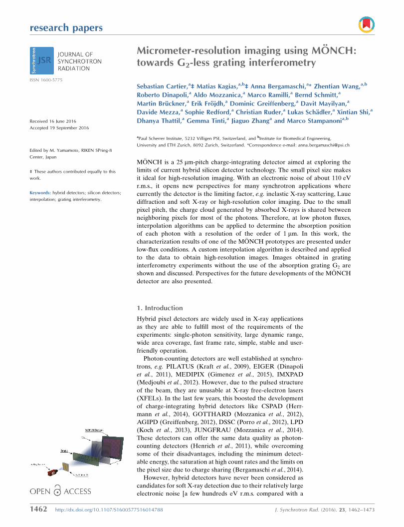
of samples containing small details. Fig. 7 shows an image of a
kidney stone of diameter a few millimeters acquired at the
TOMCAT beamline of the Swiss Light Source (Stampanoni et
al., 2007) at an energy of 16.7 keV obtained using the Si(111)
monochromator and applying additional filtering to limit the
photon flux and operate in the single-photon regime. Initially
a flat-field image of 10.5� 106 frames with an exposure time of
12 ms each was acquired. Approximately 10 � 106 photons
were found by the CFA and used to populate the �-distribu-
tion and calculate the correction map for the interpolation.
The image of the kidney stone sample was obtained using
10.5 � 106 frames with the same exposure time and approxi-
mately 6.58 � 106 photons found by the CFA.
Fig. 7(a) shows the image acquired by the CFA with the
photon hit assigned to the 25 mm-pitch pixel collecting the
maximum of the charge. The performance in terms of spatial
resolution and SNR are the same as a single-photon-counter
detector with charge-sharing suppression (Ballabriga et al.,
2007; Maj et al., 2012). The image resolution is already good,
but the improvements in the details of the image shown
in Fig. 7(b) after applying the interpolation algorithm are
clearly visible.
Unfortunately, the statistics per bin are quite poor; in fact,
photon counts are redistributed from 40 � 160 25 mm-pitch
pixels into 500 � 2000 2 mm bins, i.e. each virtual pixel accu-
mulates a factor of 156 fewer photons than in the original
image.
Although in this experiment the flux has not been properly
optimized to acquire sufficient statistics in the shortest
possible time, the acquisition time remains one of the weak
points of the method, since the detector must work in the
single-photon regime in order to interpolate.
In fact, even working at the maximum possible flux, one
would need approximately 10 frames to acquire a photon per
25 mm-pitch pixel and 6250 frames after interpolation
rebinned at 1 mm. Since the maximum frame rate of the
detector is currently limited at 1 kHz, it is necessary to
measure 6.25 s to acquire an image with on average 1 photon
per virtual pixel. One hour of measurement would allow
collection of about N = 576 photons per virtual pixel, for
SNR = N=ffiffiffiffiNp
= 24. In order to detect a contrast of �1% it
would be necessary to acquire 10000 photons per virtual pixel
with a total duration of the measurement of more than 17 h at
the current 1 kHz frame rate, 1.7 h at �10 kHz and less than
20 min at 100 kHz frame rate.
Faster frame rates could be achieved by using a 10 Gb s�1
instead of a 1 Gb s�1 transfer link, speeding up the readout by
means of faster ADCs or increasing the number of analog
output lines and performing real-time data compression on
the readout board. This is necessary in particular for the
foreseen larger area detectors in order to prevent excessive
data throughput (32 GB s�1 cm�2 at 100 kHz frame rate).
Event-driven readout is also a possibility which could be
considered, although it introduces several issues in the data
processing (e.g. leakage current subtraction) and is not
effective in compressing the data when the occupancy is high.
The limitation in the maximum detectable flux is particu-
larly restricting at synchrotrons, where it is impossible to make
use of the huge fluxes provided by imaging beamlines, while it
much better fits the low intensity generated by microfocus
X-ray tubes.
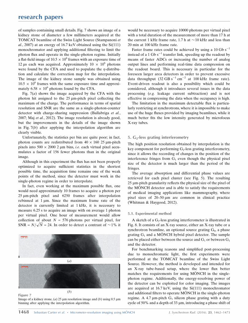
5. G2-less grating interferometry
The high position resolution obtained by interpolation is the
key component for performing G2-less grating interferometry,
since it allows the recording of changes in the position of the
interference fringes from G1 even though the physical pixel
size of the detector is much larger than the period of the
fringes.
The average absorption and differential phase values are
retrieved for each pixel cluster (see Fig. 5). The resulting
25 mm-pitch granularity reflects the physical size of the pixel of
the MONCH detector and is able to satisfy the requirements
of medical imaging applications like mammography, where
pixel sizes of 20–50 mm are common in clinical practice
(Whitman & Haygood, 2012).
5.1. Experimental method
A sketch of a G2-less grating interferometer is illustrated in
Fig. 8. It consists of an X-ray source, either an X-ray tube or a
synchrotron beamline, an optional source grating G0, a phase
grating G1 and a MONCH hybrid pixel detector. The sample
can be placed either between the source and G1 or between G1
and the detector.
For benchmarking reasons and simplified post-processing
due to monochromatic light, the first experiments were
performed at the TOMCAT beamline of the Swiss Light
Source. However, the method is developed and intended for
an X-ray tube-based setup, where the lower flux better
matches the requirements for using MONCH in the single-
photon regime. Additionally, the energy-resolving power of
the detector can be exploited for color imaging. The images
are acquired at 16.7 keV, using the Si(111) monochromator
and additional filters to operate MONCH in the single-photon
regime. A 4.7 mm-pitch G1 silicon phase grating with a duty
cycle of 50% and a depth of 33 mm, introducing a phase shift of
research papers
1468 Sebastian Cartier et al. � Micrometer-resolution imaging using MONCH J. Synchrotron Rad. (2016). 23, 1462–1473
Figure 7Image of a kidney stone, (a) 25 mm resolution image and (b) using 0.5 mmbinning after applying the interpolation algorithm.
�=2, was used for the experiment. The grating was produced at
the Laboratory of Micro and Nanotechnology of the PSI.
Compared with the standard Talbot or Talbot–Lau grating
interferometer, the analyzer grating G2 is not used. The X-ray
source illuminates the phase grating G1 producing inter-
ference fringes at defined distances zt (Talbot distances),
where they are detected by MONCH.
The experiment consists of three successive measurements
with the same exposure time:
(i) Blank, using an empty silicon wafer (without grating
structures) placed in the beam. It is used to calibrate the
interpolation algorithm by calculating the correction map as
explained in x4. The empty silicon wafer is used to compensate
the photon statistics of the following measurements,
preventing extra double counting due to higher flux if no
silicon wafer is present.
(ii) Grating, taken with only the phase grating G1 in the
beam and used as a reference for the intensity modulation
fringes.
(iii) Sample, acquired with both the sample and the grating
G1 in the beam.
The blank and grating images are required as preparation.
They do not contribute to the deposited dose on the sample
and they do not need to be repeated for new samples in cases
where the setup is unchanged.
5.2. Phase retrieval
Since the G1 grating introduces a one-dimension horizontal
modulation, after interpolation the intensity is integrated in
the vertical direction, parallel to the grating lines within the
25 mm-pitch clusters hn;mi in order to increase the statistics
and the visibility of the fringes. Also the differential phase and
the absorption signals are retrieved for each pixel cluster
hn;mi. The interpolation technique is used to make the fringes
visible, but the granularity of the final image reflects the 25 mm
segmentation of the detector.
In general, the recorded interference fringe can be
approximated by a sinusoidal signal,
I �xð Þ ¼ a �xð Þ þ b �xð Þ cos 2�=g1ð Þ�x � ’ �xð Þ� �
; ð5Þ
where g1 is the period of the recorded interference pattern,
að�xÞ contains the absorption information, bð�xÞ the scattering
or visibility reduction but also the response of the pixel cluster
due to non-uniform resolution and ’ð�xÞ the phase informa-
tion.
Igð�xÞ and Isð�xÞ represent the intensity modulation of the
grating and of the sample image, respectively, for one of the
clusters, where �x is the horizontal coordinate within the pixel
(�p=2 � �x < p=2). The goal is to retrieve the differential
phase contrast (DPC) for each pixel cluster hn;mi, i.e. the
phase difference between the sample ’hn;mis and the grating
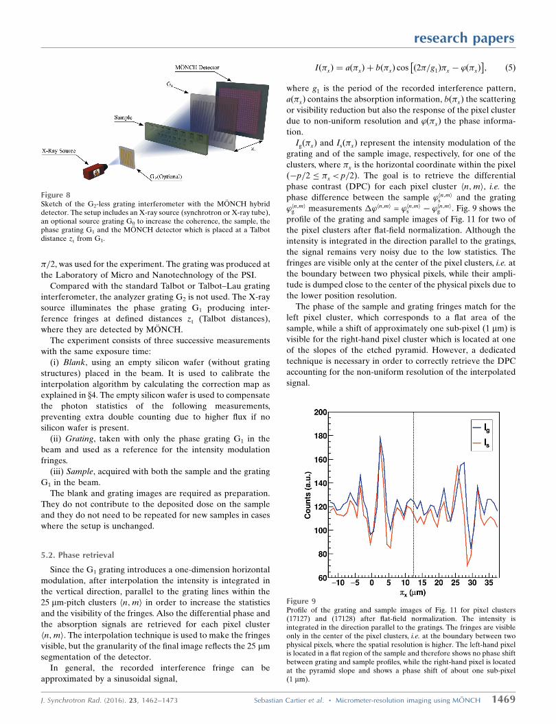
profile of the grating and sample images of Fig. 11 for two of
the pixel clusters after flat-field normalization. Although the
intensity is integrated in the direction parallel to the gratings,
the signal remains very noisy due to the low statistics. The
fringes are visible only at the center of the pixel clusters, i.e. at
the boundary between two physical pixels, while their ampli-
tude is dumped close to the center of the physical pixels due to
the lower position resolution.
The phase of the sample and grating fringes match for the
left pixel cluster, which corresponds to a flat area of the
sample, while a shift of approximately one sub-pixel (1 mm) is
visible for the right-hand pixel cluster which is located at one
of the slopes of the etched pyramid. However, a dedicated
technique is necessary in order to correctly retrieve the DPC
accounting for the non-uniform resolution of the interpolated
signal.
research papers
J. Synchrotron Rad. (2016). 23, 1462–1473 Sebastian Cartier et al. � Micrometer-resolution imaging using MONCH 1469
Figure 9Profile of the grating and sample images of Fig. 11 for pixel clusters(17127) and (17128) after flat-field normalization. The intensity isintegrated in the direction parallel to the gratings. The fringes are visibleonly in the center of the pixel clusters, i.e. at the boundary between twophysical pixels, where the spatial resolution is higher. The left-hand pixelis located in a flat region of the sample and therefore shows no phase shiftbetween grating and sample profiles, while the right-hand pixel is locatedat the pyramid slope and shows a phase shift of about one sub-pixel(1 mm).
Figure 8Sketch of the G2-less grating interferometer with the MONCH hybriddetector. The setup includes an X-ray source (synchrotron or X-ray tube),an optional source grating G0 to increase the coherence, the sample, thephase grating G1 and the MONCH detector which is placed at a Talbotdistance zt from G1.
A method based on the Hilbert transform was developed in
order to correctly retrieve the DPC, as explained in detail by
Kagias et al. (2016a). The average absorption A and differ-
ential phase P for each pixel cluster can be extracted from the
following equations,
Ahn;mi ¼Rp=2
�p=2
Is �xð Þ d�x
. Rp=2
�p=2
Ig �xð Þ d�x;
Phn;mi ¼Rp=2
�p=2
w �xð Þ arg �IsIs �xð Þ= �IgIg �xð Þ� �
d�x:
ð6Þ
Is(x) and Ig(x) are the analytical signals of the recorded
fringes, wðxÞ is an appropriate normalized weighting function
that accounts for the non-uniform resolution of the inter-
polation method, and p is the pixel pitch. The weighting
function is required to enhance the detection of the spatial
frequency of the fringes close to the pixel boundaries, while
discarding the background given by the photons absorbed in
regions where the fringes are not visible, but reduces the dose
efficiency of the technique.
In order for the above equations to be applicable, the
absorption of the sample should vary slowly within one
physical pixel compared with the period of the interference
fringe. This is a general requirement for interferometric
imaging methods that are based on the direct recording of
the interference fringe (Wen et al., 2010; Bennett et al., 2010).
However, with our method we are able to record fringes with a
few micrometers pitch which means that the maximum spatial
variations of the sample can be much higher compared with
methods utilizing large-pitch gratings.
5.3. Imaging results and quantitative validation
Various samples have been used to demonstrate the validity
of the method and also to examine the performance of the
imaging technique.
Due to the limited frame rate of the current detector
prototype, each of the three images required for the experi-
ment took about 3 h, using a sub-frame exposure time of 12 ms
and frame rate of 1 kHz, i.e. the sensor is insensitive 99% of
the time due to the speed of the current readout electronics.
The photon count per physical pixel in the final image was of
the order of 25000.
Fig. 10 shows the absorption and DPC images of a poly-
ethylene sphere with a diameter of 700 mm and a nylon fiber
taken from a toothbrush with 150 mm diameter. These samples
produce straightforward DPC signals and are therefore easy
to interpret.
For a quantitative validation of the technique, pyramids of
different sizes etched into a Si substrate were used as a sample.
Fig. 11(a) shows a scanning electron microscopy (SEM) image
of the sample. The size of the etched pyramids ranges from
50 to 350 mm and the spacing from 200 to 25 mm. It can
be observed that the largest pyramids were not etched
completely, due to porosity developing in the SiO2 mask
during the etching which limited the maximum possible
etching time. The retrieved absorption and differential phase
images are presented in Figs. 11(b) and 11(c), respectively. All
pyramids are clearly visible in both images, even the smallest
one with a size of 50 mm.
The measured differential phase values were used in order
to calculate the refraction angles of the detected photons and
compared with the theoretical values. The etched pyramids in
Si[100] have a slope of �54.73 which means that 16.7 keV
photons impinging at the edges of the pyramids will be
refracted by an angle � = �k�ffiffiffi2p
= �4.9210 mrad, where k is
the wavenumber and � the refractive index decrement for Si
research papers
1470 Sebastian Cartier et al. � Micrometer-resolution imaging using MONCH J. Synchrotron Rad. (2016). 23, 1462–1473
Figure 10Retrieved (a) absorption and (b) differential phase contrast images with apixel size of 25 mm for a polyethylene sphere with 700 mm diameter (left)and a nylon rod with 150 mm diameter (right).
Figure 11(a) SEM image of the pyramid sample. Retrieved (b) absorption and(c) differential phase contrast images with a pixel size of 25 mm for thepyramids etched in Si.
which at 16.7 keV is 1.7639 � 10�6. The measured differential
phase value of the slopes is calculated to be P = �(0.4938 �
0.0869) rad. The refractive angles can be retrieved from the
phase difference by � = Pg1 /2�zt , where zt = 15 cm; from
the experimental data this results in �exp = �(4.9249 �
0.8664) mrad demonstrating that the quantitative differential
phase information is well retrieved.
6. Conclusions
With a pixel size of 25 mm and an extremely low noise of
111 eV r.m.s., the MONCH hybrid pixel detector targets low-
energy applications where so far only CCDs and CMOS
imagers could be used. Moreover, the large amount of charge
sharing observable at this small pitch can be exploited to
interpolate the hit position of isolated photons, achieving a
spatial resolution of the order of 1 mm, as explained in detail in
x4. In x5 the high spatial resolution obtained by interpolation
is exploited for the direct measurement of the DPC in grating-
based phase contrast imaging without the use of the analyzer
grating G2. This overcomes some of the challenges of grating
interferometry which prevent it from moving into clinical
practice: low dose efficiency due to the absorption of G2,
manufacturing limitation for G2 in terms of area and aspect
ratio (i.e. absorption for hard X-rays), long acquisition times
due to multiple exposures and complex high-resolution
mechanics to perform phase stepping.
However, MONCH targets application in many other X-ray
experiments both at synchrotrons and using X-ray tubes. The
use of dynamic gain switching (Henrich et al., 2011), which
is already implemented in some of the sub-blocks of
MONCH0.2, will also allow applications at XFELs for soft
X-ray beamlines.
In particular, we foresee promising perspectives in soft
X-ray applications, for inelastic X-ray scattering or Laue
diffraction, where the detector is often the limiting element of
the experiment. Compared with the JUNGFRAU 0.4 75 mm-
pitch hybrid pixel detector, which already demonstrated a
similar noise performance (Jungmann-Smith et al., 2016), the
small pixel pitch of MONCH makes it ideal for imaging
applications. Despite the larger amount of charge sharing, the
interpolation performance decreases at lower energies due to
lower SNR. However, we expect to be able to interpolate
down to approximately 2 keV with micrometer resolution,
which makes it interesting for hard X-ray inelastic X-ray
scattering.
For Laue diffraction we expect to be able to determine the
energy of single photons with a resolution better than 220 eV
r.m.s., improved down to 220 eV=ffiffiffiffiNp
r.m.s. by averaging over
the N counts in the peak.
Concerning X-ray emission spectroscopy, larger pixels like
for JUNGFRAU 0.4 are probably more promising because
of the reduced charge sharing. However, the small pixels
provided by MONCH can increase the maximum detectable
flux. Charge sharing can also be suppressed by means of a
collimation mask or by excluding the events where charge
sharing is observed (software collimation).
6.1. Discussion and perspectives
Despite the promising results, some flaws of the current
MONCH prototype need to be fixed for improved usage in
scientific experiments, in particular for imaging:
(i) Spatial resolution. The spatial resolution depends on the
photon absorption position within the pixel (higher close to
the pixel borders where charge sharing is prominent, lower in
the pixel center). An improvement in the resolution could be
achieved by utilizing smaller pixels (e.g. 20 mm) or by enhan-
cing the charge sharing by increasing the charge collection
time. This is obtained by increasing the sensor thickness,
reducing the bias voltage or using lower X-ray energies which
are absorbed closer to the back-plane of the sensor. The
spatial resolution is also affected by the alignment of the
sensor relative to the X-ray beam due to the parallax given by
the different depth of absorption of the hard X-rays photons
through the 320 mm silicon sensor (�320 nm per 1 mdeg
misalignment).
(ii) Field of view. The field of view of the the MONCH0.2
prototype is limited to 1 mm� 4 mm. Challenges in increasing
the detector area include the bump-bonding yield, the
maximum frame rate and the data throughput. The larger
1 cm � 1 cm MONCH0.3 prototype (160 kpixel) is currently
undergoing characterization. The data transfer interface has
been upgraded from 1 Gb s�1 to 10 Gb s�1. It is read out in
parallel over 32 analog outputs and can achieve a maximum
frame rate of 6 kHz. The huge data throughput of almost
2 GB s�1 requires the development of on-the-fly CFA and
simultaneous position interpolation. In the future, we plan to
design a 3 cm � 2 cm readout ASIC which fully exploits the
recticle size offered by the manufacturing process. In the next
few years, we plan to build a MONCH detector system of 3 cm
� 4 cm by tiling together two ASICs sharing the same sensor.
The development of the proposed 3 cm � 4 cm detector will
deliver a system competitive with CCDs and CMOS imagers
for soft X-ray imaging.
(iii) Measurement time. With the current frame rate of
1 kHz, single-photon discrimination is possible up to a photon
flux of �105 photons mm�1 s�1. At this count rate the
acquisition of a high-resolution image with 1 mm2 virtual pixel
size and a dynamic range of 8-bits (256 counts subpixel�1)
takes �1440 s. However, higher-frequency readout, paralleli-
zation and faster data transfer could increase the flux by one
to two orders of magnitude and reduce the measurement time
to less than 1 min. It has to be noticed that the proposed
increase of the detector size will require more sophisticated
data acquisition and back-end systems to transfer the data and
efficiently store them. Without interpolation, MONCH can
also operate at higher fluxes, with a frame rate which over-
takes the frame rate offered by CCDs and even CMOS
imagers by orders of magnitude.
(iv) Quantum efficiency. The silicon sensors should be
optimized for the detection of soft X-rays below 3 keV which
are absorbed in the detector back-plane in the absence of an
electric field and therefore cannot be detected. Normally, the
aluminium layer can be removed and the thickness of the
research papers
J. Synchrotron Rad. (2016). 23, 1462–1473 Sebastian Cartier et al. � Micrometer-resolution imaging using MONCH 1471
n+-doping modulation can be reduced from micrometers to
tens of nanometers by specific doping techniques. The
resulting quantum efficiency can improve by almost a factor of
two at the silicon K-edge (85% absorption efficency for
200 nm-thick back-plane compared with 45% for 1 mm).
Moreover, the 320 mm silicon sensor is relatively trans-
parent for hard X-rays (59% quantum efficiency at 16.7 keV).
High-Z materials like CdTe or GaAs provide a higher
quantum efficiency (both �100% quantum efficiency at
16.7 keV and sensor thickness of 500 mm) and can be used for
applications up to 100 keV (Steadman et al., 2011; Hamann et
al., 2013). However, the quality of the high-Z sensor materials
still needs to be demonstrated and the charge collection
performance needs to be characterized in order to properly
perform interpolation.
With all the proposed improvements, MONCH promises to
equal the performance of monolithic detectors or indirect
detection systems (scintillators coupled to photodetectors) in
many X-ray applications by combining the advantages given
by direct conversion, low noise and high resolution with the
flexibility given by the well consolidated hybrid technology.
Moreover, it will outdo their performance in terms of frame
rate.
6.2. Single-shot grating interferometry
The previous discussion concerning the flaws and the
possible improvements applies also to the proposed G2-less
grating interferometry application.
Since the finest fringe period and minimal resolvable phase
shift are limited by the ultimate spatial resolution of the
detector, currently the fringes are visible only close to the
pixel borders and therefore only a fraction of the absorbed
photons can be used to retrieve the differential phase infor-
mation. This is particularly restrictive in medical imaging
applications, where the dose delivered to the patient should be
limited. Additionally, to improve the operating parameters of
the detector by enhancing the charge sharing, the use of a
phase grating with a pitch larger than the 4.7 mm currently
used would also allow a better exploitation of the position
information carried by photons absorbed in the pixel center.
A field of view of a few square centimeters is still insuffi-
cient for clinical applications. However, many imaging tech-
niques could already benefit from such a system. In the long
term, the use of through silicon vias (TSVs) could allow tiling
of ASICs on four sides, aiming at full six-inch wafer sensor
assembly with reduced gaps between the ASICs. Similar
improvements should follow also concerning the maximum
grating area, which is currently limited to four-inch wafers.
Although avoiding phase stepping, the measurement time
required in grating interferometry to operate MONCH in
single-photon regime is still very long. However, the limitation
on the maximum detectable flux is striking for direct imaging
synchrotron applications but matches well the fluxes of
microfocus X-ray tubes. Additionally, the low noise of 31 e� =
110 eV r.m.s. per pixel allows micrometer-resolution color
imaging to be performed with an energy resolution of 220 eV
r.m.s. on the 2 � 2 pixel cluster.
An improvement of the quantum efficiency for hard X-rays
is extremely important for grating interferometry and medical
examinations in general, since it brings a proportional
reduction of the dose.
Future work will also involve the replacement of the one-
dimensional phase grating with a two-dimensional periodic
structure. This can allow the retrieval of quantitative differ-
ential phase in two directions and can be used to obtain
quantitative phase values without integration artifacts
(Kottler et al., 2007; Kagias et al., 2016b).
All these improvements will result in significant steps
towards a broad implementation of phase contrast imaging in
the medical field and beyond.
Acknowledgements
We thank G. Mikuljan, A. Astolfo and F. Marone from Paul
Scherrer Institut for their support in the experiments and
K. Jefimovs for his input regarding the sample and grating
fabrication. We thank the staff of the SYRMEP beamline
of the Elettra synchrotron facility (Trieste, Italy) for their
support during the calibration measurements, in particular
L. Rigon and R. H. Menk. Part of this work has been
supported by the ERC grant ERC-2012-StG 310005-
PhaseX.
References
Abrami, A., Arfelli, F., Barroso, R., Bergamaschi, A., Bille, F.,Bregant, P., Brizzi, F., Casarin, K., Castelli, E., Chenda, V., DallaPalma, L., Dreossi, D., Fava, C., Longo, R., Mancini, L., Menk,R.-H., Montanari, F., Olivo, A., Pani, S., Pillon, A., Quai, E., RenKaiser, S., Rigon, L., Rokvic, T., Tonutti, M., Tromba, G., Vascotto,A., Venanzi, C., Zanconati, F., Zanetti, A. & Zanini, F. (2005). Nucl.Instrum. Methods Phys. Res. A, 548, 221–227.
Ballabriga, R., Campbell, M., Heijne, E. H. M., Llopart, X. & Tlustos,L. (2007). IEEE Trans. Nucl. Sci. 54, 1824–1829.
Belau, E., Klanner, R., Lutz, G., Neugebauer, E., Seebrunner, H.,Wylie, A., Bohringer, T., Hubbeling, L., Weilhammer, P., Kemmer,J., Kotz, U. & Riebesell, M. (1983). Nucl. Instrum. Methods Phys.Res. 214, 253–260.
Bennett, E. E., Kopace, R., Stein, A. F. & Wen, H. (2010). Med. Phys.37, 6047–6054.
Bergamaschi, A., Broennimann, C., Dinapoli, R., Eikenberry, E.,Gozzo, F., Henrich, B., Kobas, M., Kraft, P., Patterson, B. & Schmitt,B. (2008). Nucl. Instrum. Methods Phys. Res. A, 591, 163–166.
Bergamaschi, A., Cartier, S., Dinapoli, R., Greiffenberg, D., Johnson,I., Mezza, D., Mozzanica, A., Schmitt, B., Shi, X., Jungmann-Smith,J. & Tinti, G. (2014). Synchrotron Radiat. News, 27, 3.
Bergamaschi, A., Cartier, S., Dinapoli, R., Greiffenberg, D.,Jungmann-Smith, J., Mezza, D., Mozzanica, A., Schmitt, B., Shi,X. & Tinti, G. (2015). J. Instrum. 10, C01033.
Buttler, W., Hosticka, B. & Lutz, G. (1990). Nucl. Instrum. MethodsPhys. Res. A, 288, 187–190.
Cartier, S., Bergamaschi, A., Dinapoli, R., Greiffenberg, D., Johnson,I., Jungmann, J. H., Mezza, D., Mozzanica, A., Schmitt, B., Shi, X.,Stampanoni, M., Sun, J. & Tinti, G. (2014). J. Instrum. 9, C05027.
research papers
1472 Sebastian Cartier et al. � Micrometer-resolution imaging using MONCH J. Synchrotron Rad. (2016). 23, 1462–1473
Cartier, S., Bergamaschi, A., Dinapoli, R., Greiffenberg, D., Johnson,I., Jungmann-Smith, J., Mezza, D., Mozzanica, A., Shi, X., Tinti, G.,Schmitt, B. & Stampanoni, M. (2015). J. Instrum. 10, C03022.
Dinapoli, R., Bergamaschi, A., Cartier, S., Greiffenberg, D., Johnson,I., Jungmann, J. H., Mezza, D., Mozzanica, A., Schmitt, B., Shi, X. &Tinti, G. (2014). J. Instrum. 9, C05015.
Dinapoli, R., Bergamaschi, A., Henrich, B., Horisberger, R., Johnson,I., Mozzanica, A., Schmid, E., Schmitt, B., Schreiber, A., Shi, X. &Theidel, G. (2011). Nucl. Instrum. Methods Phys. Res. A, 650, 79–83.
Gimenez, E. N., Ballabriga, R., Blaj, G., Campbell, M., Dolbnya, I.,Frodjh, E., Horswell, I., Llopart, X., Marchal, J., McGrath, J., Omar,D., Plackett, R., Sawhney, K. & Tartoni, N. (2015). IEEE Trans.Nucl. Sci. 62, 1413–1421.
Greiffenberg, D. (2012). J. Instrum. 7, C01103.Hamann, E., Cecilia, A., Zwerger, A., Fauler, A., Tolbanov, O.,
Tyazhev, A., Shelkov, G., Graafsma, H., Baumbach, T. & Fiederle,M. (2013). J. Phys. Chem. Soc. 425, 62015.
Henrich, B., Becker, J., Dinapoli, R., Goettlicher, P., Graafsma, H.,Hirsemann, H., Klanner, R., Krueger, H., Mazzocco, R., Mozza-nica, A., Perrey, H., Potdevin, G., Schmitt, B., Shi, X., Srivastava,A. K., Trunk, U. & Youngman, C. (2011). Nucl. Instrum. MethodsPhys. Res. A, 633, S11–S14.
Herrmann, S., Hart, P., Dragone, A., Freytag, D., Herbst, R., Pines, J.,Weaver, M., Carini, G. A., Thayer, J. B., Shawn, O., Kenney, C. &Haller, G. (2014). J. Phys. Conf. Ser. 493, 012013.
Jungmann-Smith, J. H., Bergamaschi, A., Bruckner, M., Cartier, S.,Dinapoli, R., Greiffenberg, D., Huthwelker, T., Maliakal, D.,Mayilyan, D., Medjoubi, K., Mezza, D., Mozzanica, A., Ramilli, M.,Ruder, C., Schadler, L., Schmitt, B., Shi, X. & Tinti, G. (2016).J. Synchrotron Rad. 23, 385–394.
Kagias, M., Cartier, S., Wang, Z., Bergamaschi, A., Dinapoli, R.,Mozzanica, A., Schmitt, B. & Stampanoni, M. (2016). Appl. Phys.Lett. 108, 234102.
Kagias, M., Wang, Z., Villanueva-Perez, P., Jefimovs, K. &Stampanoni, M. (2016b). Phys. Rev. Lett. 116, 093902.
Koch, A., Hart, M., Nicholls, T., Angelsen, C., Coughlan, J., French,M., Hauf, S., Kuster, M., Sztuk-Dambietz, J., Turcato, M., Carini,G. A., Chollet, M., Herrmann, S. C., Lemke, H. T., Nelson, S., Song,S., Weaver, M., Zhu, D., Meents, A. & Fischer, P. (2013). J. Instrum.8, C11001.
Kottler, C., David, C., Pfeiffer, F. & Bunk, O. (2007). Opt. Express, 15,1175–1181.
Kraft, P., Bergamaschi, A., Broennimann, Ch., Dinapoli, R.,Eikenberry, E. F., Henrich, B., Johnson, I., Mozzanica, A.,Schleputz, C. M., Willmott, P. R. & Schmitt, B. (2009). J.Synchrotron Rad. 16, 368–375.
Lutz, G. (1999). Semiconductor Radiation Detectors: Device Physics.Berlin: Springer.
Maj, P., Baumbaugh, A., Deptuch, G., Grybos, P. & Szczygiel, R.(2012). J. Instrum. 7, C12020.
Medjoubi, K., Thompson, A., Berar, J.-F., Clemens, J.-C., Delpierre,P., Da Silva, P., Dinkespiler, B., Fourme, R., Gourhant, P.,Guimaraes, B., Hustache, S., Idir, M., Itie, J.-P., Legrand, P.,Menneglier, C., Mercere, P., Picca, F. & Samama, J.-P. (2012).J. Synchrotron Rad. 19, 323–331.
Mozzanica, A., Bergamaschi, A., Cartier, S., Dinapoli, R., Greiffen-berg, D., Johnson, I., Jungmann, J., Maliakal, D., Mezza, D., Ruder,C., Schaedler, L., Schmitt, B., Shi, X. & Tinti, G. (2014). J. Instrum.9, C05010.
Mozzanica, A., Bergamaschi, A., Dinapoli, R., Graafsma, H.,Greiffenberg, D., Henrich, B., Johnson, I., Lohmann, M., Valeria,R., Schmitt, B. & Xintian, S. (2012). J. Instrum. 7, C01019.
Pfeiffer, F., Weitkamp, T., Bunk, O. & David, C. (2006). Nat. Phys. 2,258–261.
Porro, M., Andricek, L., Aschauer, S., Bayer, M., Becker, J., Bombelli,L., Castoldi, A., De Vita, G., Diehl, I., Erdinger, F., Facchinetti, S.,Fiorini, C., Fischer, P., Gerlach, T., Graafsma, H., Guazzoni, C.,Hansen, K., Kalavakuru, P., Klar, H., Kugel, A., Lechner, P.,Lemke, M., Lutz, G., Manghisoni, M., Mezza, D., Muntefering, D.,Pietsch, U., Quartieri, E., Randall, M., Re, V., Reckleben, C.,Sandow, C., Soldat, J., Struder, L., Szymanski, J., Weidenspointner,G. & Wunderer, C. (2012). IEEE Trans. Nucl. Sci. 59, 3339–3351.
Quaglia, R., Bombelli, L., Busca, P., Fiorini, C., Occhipinti, M.,Giacomini, G., Ficorella, F., Picciotto, A. & Piemonte, C. (2015).IEEE Trans. Nucl. Sci. 62, 221–227.
Radeka, V. (1988). Annu. Rev. Nucl. Part. Sci. 38, 217–277.Roessl, E., Daerr, H., Koehler, T., Martens, G. & van Stevendaal, U.
(2014). Philos. Trans. R. Soc. A, 372, 20130033.Schubert, A., Bergamaschi, A., David, C., Dinapoli, R., Elbracht-
Leong, S., Gorelick, S., Graafsma, H., Henrich, B., Johnson, I.,Lohmann, M., Mozzanica, A., Radicci, V., Rassool, R., Schadler, L.,Schmitt, B., Shi, X. & Sobott, B. (2012). J. Synchrotron Rad. 19,359–365.
Stampanoni, M., Groso, A., Isenegger, A., Mikuljan, G., Chen, Q.,Meister, D., Lange, M., Betemps, R., Henein, S. & Abela, R. (2007).AIP Conf. Proc. 879, 848–851.
Steadman, R., Herrmann, C., Mulhens, O. & Maeding, D. G. (2011).Nucl. Instrum. Methods Phys. Res. A, 648, S211–S215.
Weitkamp, T., Diaz, A., David, C., Pfeiffer, F., Stampanoni, M.,Cloetens, P. & Ziegler, E. (2005). Opt. Express, 13, 6296–6304.
Wen, H. H., Bennett, E. E., Hegedus, M. M. & Carroll, S. C. (2008).IEEE Trans. Med. Imaging, 27, 997–1002.
Wen, H. H., Bennett, E. E., Kopace, R., Stein, A. F. & Pai, V. (2010).Opt. Lett. 35, 1932–1934.
Whitman, G. J. & Haygood, T. M. (2012). Digital Mammography. APractical Approach. Cambridge University Press.
research papers
J. Synchrotron Rad. (2016). 23, 1462–1473 Sebastian Cartier et al. � Micrometer-resolution imaging using MONCH 1473