Politecnico di Torino Porto Institutional Repository [Proceeding] Microprocessor fault-tolerance via on-the-fly partial reconfiguration Original Citation: Di Carlo S., Miele A., Prinetto P., Trapanese A. (2010). Microprocessor fault-tolerance via on-the-fly partial reconfiguration. In: IEEE 15th European Test Symposium (ETS), Praga, CZ, 24-28 May 2010. pp. 201-206 Availability: This version is available at : http://porto.polito.it/2380367/ since: January 2011 Publisher: IEEE Computer Society Published version: DOI:10.1109/ETSYM.2010.5512759 Terms of use: This article is made available under terms and conditions applicable to Open Access Policy Article ("Public - All rights reserved") , as described at http://porto.polito.it/terms_and_conditions. html Porto, the institutional repository of the Politecnico di Torino, is provided by the University Library and the IT-Services. The aim is to enable open access to all the world. Please share with us how this access benefits you. Your story matters. (Article begins on next page)
Transcript
Politecnico di Torino
Porto Institutional Repository
[Proceeding] Microprocessor fault-tolerance via on-the-fly partialreconfiguration
Original Citation:Di Carlo S., Miele A., Prinetto P., Trapanese A. (2010). Microprocessor fault-tolerance via on-the-flypartial reconfiguration. In: IEEE 15th European Test Symposium (ETS), Praga, CZ, 24-28 May2010. pp. 201-206
Availability:This version is available at : http://porto.polito.it/2380367/ since: January 2011
Publisher:IEEE Computer Society
Published version:DOI:10.1109/ETSYM.2010.5512759
Terms of use:This article is made available under terms and conditions applicable to Open Access Policy Article("Public - All rights reserved") , as described at http://porto.polito.it/terms_and_conditions.html
Porto, the institutional repository of the Politecnico di Torino, is provided by the University Libraryand the IT-Services. The aim is to enable open access to all the world. Please share with us howthis access benefits you. Your story matters.
Abstract—This paper presents a novel approach to exploitFPGA dynamic partial reconfiguration to improve the faulttolerance of complex microprocessor-based systems, with noneed to statically reserve area to host redundant components.The proposed method not only improves the survivability ofthe system by allowing the online replacement of defective keyparts of the processor, but also provides performance gracefuldegradation by executing in software the tasks that were executedin hardware before a fault and the subsequent reconfigurationhappened. The advantage of the proposed approach is thatthanks to a hardware hypervisor, the CPU is totally unawareof the reconfiguration happening in real-time, and there’s nodependancy on the CPU to perform it. As proof of conceptsa design using this idea has been developed, using the LEON3open-source processor, synthesized on a Virtex 4 FPGA.
Index Terms—fault tolerance, partial reconfiguration, self-repair architectures, graceful degradation
I. INTRODUCTION
Embedded systems are nowdays widely used for manysafety-critical applications that impose very strict, often con-flicting, requirements, including fault-tolerance, real-time dataprocessing, and reduced use of resources and power.
Several solutions do exist to guarantee hardware fault tol-erance depending on the requirements of the target design.Neverthless, choosing among them often requires compro-mises in terms of cost, performance, fault detection delay,etc. Moreover, most of these techniques have been originallydeveloped to be applied on ASICs (Application Specific Inte-grated Circuit), while nowdays several custom embedded SoCs(System on Chip) are realized on FPGAs (Field ProgrammableGate Array). Even if the proposed techniques still mantaintheir effectiveness, they are not optimized to take advantageof most recent FPGA technologies, and they do not considerthe nature of FPGA-specific faults.
Although the symptoms of transient or permanent faultson FPGAs can be categorized in component and controlfaults as proposed in [1], their source can be different andmore complex to discover than on traditional ASICs. In aFPGA design, a permanent fault does not necessarily identifya damaged circuit; it can be generated by a bit-flipping ofthe FPGA configuration memory. Even if a more generalapproach could be used, traditional fault detection, diagnosis,and recovery methods for SRAM-based FPGAs tend to be very
defect-tolerance oriented and technology specific. In [2] theauthors review many fault detection mechanisms for FPGAs,mostly aiming at ensuring defect tolerance, while for faulttolerance they advise that a system level or a board levelsolution would be more effective and easy to implement thana low-level one.
A key technology enabling a new and generalized fault-tolerance architecture for FPGA SoCs is the “glitch-free”Dynamic Partial Reconfiguration feature of modern FPGAs[17], [16], [15]. Such a feature allows time-sharing of apredefined reconfigurable area on the FPGA fabric betweenmultiple hardware instances. This feature has been used withsuccess in some experimental designs ([3], [4]), but its fullpotential on the dependability side is yet to be exploited.
The present paper proposes a method to improve micropro-cessors fault tolerance through a self-repair strategy enabledby dynamic partial reconfiguration. The general idea is thatwhen a pipeline stage is found to be defective, it is on-the-flyreplaced by a new one, mapped into a reconfigurable area.In this way the spare unit is placed on the chip on demand,while its area can be used by other components during normaloperation.
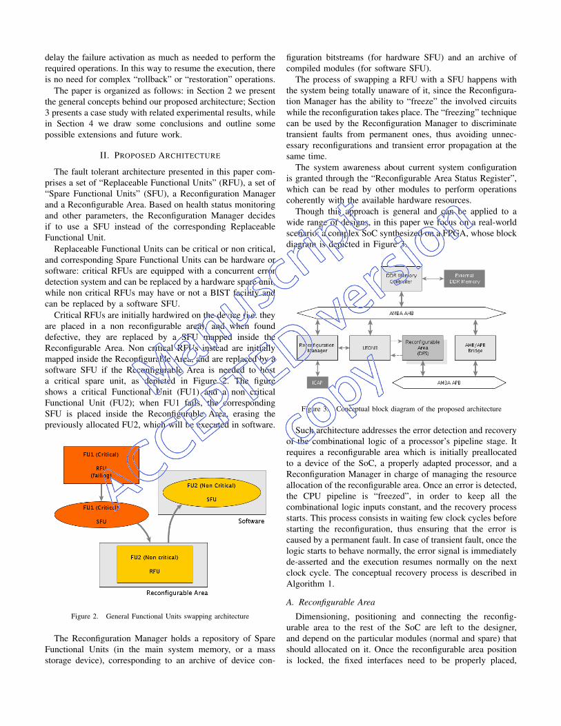
Figure 1. Error detection timing ( c�IEEE 2001, from [1])
Using as reference the taxonomy introduced in [5] and de-picted in Figure 1, the proposed architecture aims at detectingan error and at correcting the fault that generated it throughthe means of reconfiguration before the error propagates andcauses a failure. Typically the time between the DetectionActivation and Failure Activation is too small to accomodate adevice reconfiguration, thus a “freezing” technique is used to
delay the failure activation as much as needed to perform therequired operations. In this way to resume the execution, thereis no need for complex “rollback” or “restoration” operations.
The paper is organized as follows: in Section 2 we presentthe general concepts behind our proposed architecture; Section3 presents a case study with related experimental results, whilein Section 4 we draw some conclusions and outline somepossible extensions and future work.
II. PROPOSED ARCHITECTURE
The fault tolerant architecture presented in this paper com-prises a set of “Replaceable Functional Units” (RFU), a set of“Spare Functional Units” (SFU), a Reconfiguration Managerand a Reconfigurable Area. Based on health status monitoringand other parameters, the Reconfiguration Manager decidesif to use a SFU instead of the corresponding ReplaceableFunctional Unit.
Replaceable Functional Units can be critical or non critical,and corresponding Spare Functional Units can be hardware orsoftware: critical RFUs are equipped with a concurrent errordetection system and can be replaced by a hardware spare unit,while non critical RFUs may have or not a BIST facility andcan be replaced by a software SFU.
Critical RFUs are initially hardwired on the device (i.e. theyare placed in a non reconfigurable area), and when founddefective, they are replaced by a SFU mapped inside theReconfigurable Area. Non critical RFUs instead are initiallymapped inside the Reconfigurable Area, and are replaced by asoftware SFU if the Reconfigurable Area is needed to hosta critical spare unit, as depicted in Figure 2. The figureshows a critical Functional Unit (FU1) and a non criticalFunctional Unit (FU2); when FU1 fails, the correspondingSFU is placed inside the Reconfigurable Area, erasing thepreviously allocated FU2, which will be executed in software.
Figure 2. General Functional Units swapping architecture
The Reconfiguration Manager holds a repository of SpareFunctional Units (in the main system memory, or a massstorage device), corresponding to an archive of device con-
figuration bitstreams (for hardware SFU) and an archive ofcompiled modules (for software SFU).
The process of swapping a RFU with a SFU happens withthe system being totally unaware of it, since the Reconfigura-tion Manager has the ability to “freeze” the involved circuitswhile the reconfiguration takes place. The “freezing” techniquecan be used by the Reconfiguration Manager to discriminatetransient faults from permanent ones, thus avoiding unnec-essary reconfigurations and transient error propagation at thesame time.
The system awareness about current system configurationis granted through the “Reconfigurable Area Status Register”,which can be read by other modules to perform operationscoherently with the available hardware resources.
Though this approach is general and can be applied to awide range of designs, in this paper we focus on a real-worldscenario: a complex SoC synthesized on a FPGA, whose blockdiagram is depicted in Figure 3.
Figure 3. Conceptual block diagram of the proposed architecture
Such architecture addresses the error detection and recoveryof the combinational logic of a processor’s pipeline stage. Itrequires a reconfigurable area which is initially preallocatedto a device of the SoC, a properly adapted processor, and aReconfiguration Manager in charge of managing the resourceallocation of the reconfigurable area. Once an error is detected,the CPU pipeline is “freezed”, in order to keep all thecombinational logic inputs constant, and the recovery processstarts. This process consists in waiting few clock cycles beforestarting the reconfiguration, thus ensuring that the error iscaused by a permanent fault. In case of transient fault, once thelogic starts to behave normally, the error signal is immediatelyde-asserted and the execution resumes normally on the nextclock cycle. The conceptual recovery process is described inAlgorithm 1.
A. Reconfigurable Area
Dimensioning, positioning and connecting the reconfig-urable area to the rest of the SoC are left to the designer,and depend on the particular modules (normal and spare) thatshould allocated on it. Once the reconfigurable area positionis locked, the fixed interfaces need to be properly placed,
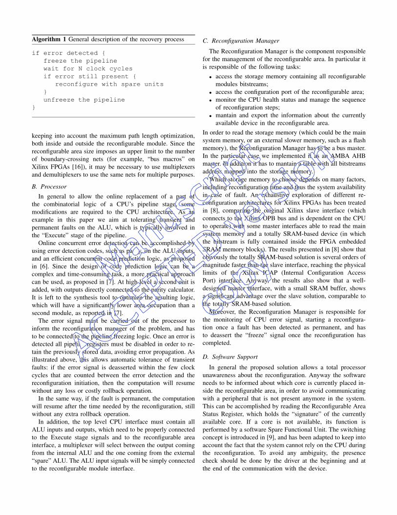
Algorithm 1 General description of the recovery process
if error detected {
freeze the pipeline
wait for N clock cycles
if error still present {
reconfigure with spare units
}
unfreeze the pipeline
}
keeping into account the maximum path length optimization,both inside and outside the reconfigurable module. Since thereconfigurable area size imposes an upper limit to the numberof boundary-crossing nets (for example, “bus macros” onXilinx FPGAs [16]), it may be necessary to use multiplexersand demultiplexers to use the same nets for multiple purposes.
B. ProcessorIn general to allow the online replacement of a part of
the combinatorial logic of a CPU’s pipeline stage, somemodifications are required to the CPU architecture. As anexample in this paper we aim at tolerating transient andpermanent faults on the ALU, which is typically involved inthe “Execute” stage of the pipeline.
Online concurrent error detection can be accomplished byusing error detection codes, such as parity, on the ALU inputs,and an efficient concurrent code prediction logic, as proposedin [6]. Since the design of code prediction logic can be acomplex and time-consuming task, a more practical approachcan be used, as proposed in [7]. At high level a second unit isadded, with outputs directly connected to the parity calculator.It is left to the synthesis tool to optimize the resulting logic,which will have a significantly lower area occupation than asecond module, as reported in [7].
The error signal must be carried out of the processor toinform the reconfiguration manager of the problem, and hasto be connected to the pipeline freezing logic. Once an error isdetected all pipeline registers must be disabled in order to re-tain the previously stored data, avoiding error propagation. Asillustrated above, this allows automatic tolerance of transientfaults: if the error signal is deasserted within the few clockcycles that are counted between the error detection and thereconfiguration initiation, then the computation will resumewithout any loss or costly rollback operation.
In the same way, if the fault is permanent, the computationwill resume after the time needed by the reconfiguration, stillwithout any extra rollback operation.
In addition, the top level CPU interface must contain allALU inputs and outputs, which need to be properly connectedto the Execute stage signals and to the reconfigurable areainterface, a multiplexer will select between the output comingfrom the internal ALU and the one coming from the external“spare” ALU. The ALU input signals will be simply connectedto the reconfigurable module interface.
C. Reconfiguration Manager
The Reconfiguration Manager is the component responsiblefor the management of the reconfigurable area. In particular itis responsible of the following tasks:
• access the storage memory containing all reconfigurablemodules bitstreams;
• access the configuration port of the reconfigurable area;• monitor the CPU health status and manage the sequence
of reconfiguration steps;• mantain and export the information about the currently
available device in the reconfigurable area.In order to read the storage memory (which could be the mainsystem memory, or an external slower memory, such as a flashmemory), the Reconfiguration Manager has to be a bus master.In the particular case we implemented it as an AMBA AHBmaster. In addition it has to mantain a table with all bitstreamsaddress mapped into the storage memory.
Which storage memory to choose depends on many factors,including reconfiguration time and thus the system availabilityin case of fault. An exhaustive exploration of different re-configuration architectures for Xilinx FPGAs has been treatedin [8], comparing the original Xilinx slave interface (whichconnects to the Xilinx OPB bus and is dependent on the CPUto operate) with some master interfaces able to read the mainsystem memory and a totally SRAM-based device (in whichthe bitstream is fully contained inside the FPGA embeddedSRAM memory blocks). The results presented in [8] show thatobivously the totally SRAM-based solution is several orders ofmagnitude faster than the slave interface, reaching the physicallimits of the Xilinx ICAP (Internal Configuration AccessPort) interface. Anyway, the results also show that a well-designed master interface, with a small SRAM buffer, showsa significant advantage over the slave solution, comparable tothe totally SRAM-based solution.
Moreover, the Reconfiguration Manager is responsible forthe monitoring of CPU error signal, starting a reconfigura-tion once a fault has been detected as permanent, and hasto deassert the “freeze” signal once the reconfiguration hascompleted.
D. Software Support
In general the proposed solution allows a total processorunawareness about the reconfiguration. Anyway the softwareneeds to be informed about which core is currently placed in-side the reconfigurable area, in order to avoid communicatingwith a peripheral that is not present anymore in the system.This can be accomplished by reading the Reconfigurable AreaStatus Register, which holds the “signature” of the currentlyavailable core. If a core is not available, its function isperformed by a software Spare Functional Unit. The switchingconcept is introduced in [9], and has been adapted to keep intoaccount the fact that the system cannot rely on the CPU duringthe reconfiguration. To avoid any ambiguity, the presencecheck should be done by the driver at the beginning and atthe end of the communication with the device.
III. CASE STUDY AND EXPERIMENTAL RESULTS
As a proof of concepts, we implemented the architecturedescribed in the previous section using a SoC based on theLEON3 CPU ([10], [11]) in order to tolerate the ALU faultsby replacing a previously allocated DES (Data EncryptionStandard) crypto-core. According to the taxonomy previouslyintroduced, we identify the ALU as a critical RFU, while theDES crypto-core as a non-critical RFU. Both of them havethe corresponding SFUs (hardware for the ALU, software forthe DES core). We decided to use this example because of theself-contained and general nature of both components, whichalso have a comparable area occupation. The resulting designhas been synthesized and tested on a Xilinx Virtex 4 FPGA[17].
A. Processor architecture adaptation
LEON3 is a highly configurable 32-bit processor coreconforming to the SPARC V8 architecture. It is designed forembedded applications, combining high performance with lowcomplexity and low power consumption.
The LEON CPU is widely used in the aerospace industryand its fault-tolerant version has been validated through strictradiation tests [12]. Anyway, the implemented fault-tolerancetechniques address typical radiation-induced ASIC faults in-volving sequential logic, only. This choice was motivated bythe fact that the probability of a SEU on the combinationallogic propagating into registers on a clock edge is low asreported in [13]. This assumption becomes less significantif the circuit is synthesized on a FPGA. A SEU on theconfiguration memory may cause permanent faults on the“combinational logic” of the CPU. The only configurationof the fault-tolerant LEON architecture that provides greaterprotection against this kind of faults is the master-checkermode [12], [1] (using 2 CPUs), which has a 100% areaoverhead, thus its use is limited to applications extremelydemanding in terms of error detection.
Its pipeline is composed of 7 stages (Fetch, Decode, Reg-ister Access, Execute, Memory, Exception, Write Back).
In order to keep the complexity low, thus fitting the FPGAavailable for the implementation, the LEON3 has been config-ured with a minimal setup (no hardware MUL/DIV unit andno cache).
Due to the particular description style used in Gaislerlibraries [14], the whole processor pipeline is described in abehavioral way, with just 2 processes, one implementing thefull pipeline stages functionality, and the other one implement-ing the sequential logic.
This particular style showed both advantages and disadvan-tages for the purposes of our design: on one side it allowedthe easy implementation of the pipeline freezing logic, with asimple modification to the “sequential” process; on the otherone, it required additional reverse engineering work on the“combinational” process in order to isolate the ALU/shifterlogic from the other logic implemented in the Execute stageof the pipeline.
Once the functionality has been clearly identified, a newentity (the hardware SFU) with the minimal interface toprovide the same functionality has been developed, whichimplements the following operations:
This unit has been set to be mapped on the reconfigurable areain case of fault detection. Moreover, following the approachsuggested in [7], another “sample” of this unit has beeninserted together with parity calculators on the input and onthe output in order to provide error detection, leaving to thesynthesis tools the task of optimizing the resulting logic. Thissimple scheme has been used because of its straightforwardimplementation and acceptable area overhead. In a moresophisticated architecture a Berger code based solution couldbe adopted, as suggested in [1].
The last modification had the scope of driving “out” of theCPU all signals needed to properly connect the external ALU.Outgoing signals are simply driven by the original signals,even if the external ALU is not present, while the incomingsignals are connected to a 2-way multiplexer (implemented asa simple “if” statement in the combinational circuit).
To implement the pipeline freezing logic, the “freeze” signalhas been conceptually connected to the enable input of pipelineregisters. Practically the sequential process has been modifiedto take into account that if the freeze signal is high, no actionhas to be done in that process.
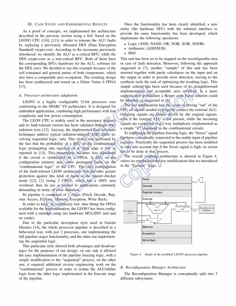
The overall resulting architecture is showed in Figure 4,where we emphasized the key modifications that we introducedin the “Execute” stage.
Figure 4. Detail of the modified LEON3 processor pipeline
B. Reconfiguration Manager Architecture
The Reconfiguration Manager is conceptually split into 3different subsystems:
• storage memory read and configuration memory writesystems;
• processor pipeline freezing control;• software support facilities.
The component is equipped with 2 different interfaces to theAMBA bus. At the same time it is an AHB master and an APBslave; the master interface is used to fetch the configurationbitstream from the storage memory (the main system memoryor another external memory), while the slave interface is usedto provide the software support facilities.
Access to the FPGA configuration memory is ensuredthrough the 32-bit Virtex 4 ICAP port [17], which is instan-tiated as a black-box and mapped on the target device duringplace&routing. A buffer is used to store temporary bitstreamdata in order to achieve high performance, since this port canwrite up 32 bits per clock cycle [15].
Finally, the pipeline freezing control logic is responsible ofboth blocking the CPU operation during the reconfigurationand restoring it once it is completed. During normal operationthe error signal is connected both to the ReconfigurationManager and the pipeline “freeze” signal: as soon as theerror signal is asserted, the pipeline is blocked and the Re-configuration Manager starts an internal timer to check if thefault is permanent or transient. If at the end of the detectionwindow the error is still present, the Reconfiguration Manageroverrides the freeze signal to ensure that any glitch that mayoccur during reconfiguration doesn’t propagate to the registers,and starts the reconfiguration.
C. Top Level Design and Reconfigurable Modules
Given the particular toolchain used for the synthesis on aXilinx device [16], the top level design had to be modifiedby using bus macros to connect the static and reconfigurablepart, which is instantiated as a black box. During place &routing the reconfigurable area size has been set, and the busmacros had to be statically placed on the boundary; during theplacement we kept into account the effects that the placementof bus macros have on the resulting layouts of both the staticand reconfigurable parts.
The RFUs/SFUs that need to be hosted inside the recon-figurable area need almost no modification compared to anormal design. The only requirement is that they must sharethe same entity interface declaration: the APB DES interfacemust contain the ALU interface signals, and the external ALUinterface must contain the APB signals, even if these are leftunconnected inside the entity.
In order to reduce the number of signals crossing thereconfigurable area boundary, the APB interface has beensplitted in a static and a dynamic part: the static one containsfixed configuration data used for PnP (Plug and Play) devicedetection, while the dynamic part is used for actual datatransfers, interrupt routing and device addressing, and is theonly one that actually passes the reconfigurable area boundarythrough bus macros.
D. Experimental ResultsThe system has been synthesized on the Xilinx ML403
board, equipped with the XC4VFX12 FPGA [17] and severalexperiments have been executed, in order to validate theconcepts introduced in previous sections. The final designoccupied almost all of the logic resources available on theFPGA (as reported in Table I), and the operating frequencyremained unchanged (66MHz) compared to the static referencedesign provided with Gaisler libraries for that board.
Virtex 4 SlicesDevice capacity 5472
Static 3426Reconfigurable Area Capacity 536
DES 313External ALU 212
Table IFPGA RESOURCES ALLOCATION
The system has been tested with a bare C prototype programwhich executed a full DES encryption/decryption cycle; theprogram included all the facilities to measure the executiontimes and to dynamically use the software version if thehardware device is not present anymore. Monitoring executiontimes allowed us to quantify the performance degradation dueto the use of software libraries instead of the hardware device,and to analyze the reconfiguration time impact on the wholeexecution time.
DES encryption (20KB plain text) TimePre-Reconfig (Hardware) 183 msPost-Reconfig (Software) 1500 ms
Measurements showed that the system is able to keepworking normally after a reconfiguration, since only the DESencryption/decryption time is affected. Table II shows oneorder of magnitude performance degradation due to the lackof hardware support). It is interesting to note that the resultinglayout kept working at the original clock frequency, which hasbeen set with a wide safety margin over critical path length.
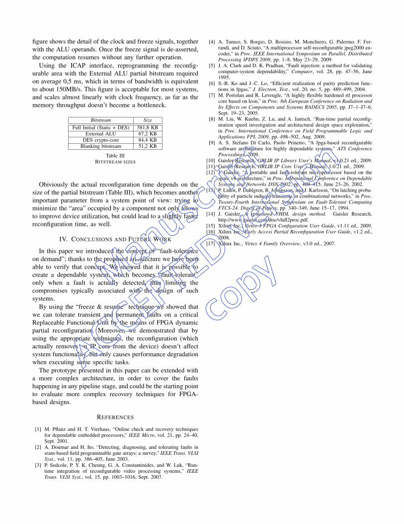
Figure 5. Simulation of the pipeline freezing logic (detail of ALU operands)
To simulate a fault, the error signal has been connected toone of the board switches instead of the error detection logic.This allowed us to cause a full reconfiguration cycle duringthe execution of the program. As the simulation results showin Figure 5, the freezing logic allows keeping constant thecombinational circuits inputs during the reconfiguration. The
figure shows the detail of the clock and freeze signals, togetherwith the ALU operands. Once the freeze signal is de-asserted,the computation resumes without any further operation.
Using the ICAP interface, reprogramming the reconfig-urable area with the External ALU partial bitstream requiredon average 0,5 ms, which in terms of bandwidth is equivalentto about 150MB/s. This figure is acceptable for most systems,and scales almost linearly with clock frequency, as far as thememory throughput doesn’t become a bottleneck.
Obiviously the actual reconfiguration time depends on thesize of the partial bitstream (Table III), which becomes anotherimportant parameter from a system point of view: trying tominimize the “area” occupied by a component not only allowsto improve device utilization, but could lead to a slightly fasterreconfiguration time, as well.
IV. CONCLUSIONS AND FUTURE WORK
In this paper we introduced the concept of “fault-toleranceon demand”; thanks to the proposed architecture we have beenable to verify that concept. We showed that it is possible tocreate a dependable system, which becomes “fault-tolerant”only when a fault is actually detected, thus limiting thecompromises typically associated with the design of suchsystems.
By using the “freeze & resume” technique we showed thatwe can tolerate transient and permanent faults on a criticalReplaceable Functional Unit by the means of FPGA dynamicpartial reconfiguration. Moreover, we demonstrated that byusing the appropriate techniques, the reconfiguration (whichactually removes an IP core from the device) doesn’t affectsystem functionality, but only causes performance degradationwhen executing some specific tasks.
The prototype presented in this paper can be extended witha more complex architecture, in order to cover the faultshappening in any pipeline stage, and could be the starting pointto evaluate more complex recovery techniques for FPGA-based designs.
REFERENCES
[1] M. Pflanz and H. T. Vierhaus, “Online check and recovery techniquesfor dependable embedded processors,” IEEE Micro, vol. 21, pp. 24–40,Sept. 2001.
[2] A. Doumar and H. Ito, “Detecting, diagnosing, and tolerating faults insram-based field programmable gate arrays: a survey,” IEEE Trans. VLSISyst., vol. 11, pp. 386–405, June 2003.
[3] P. Sedcole, P. Y. K. Cheung, G. A. Constantinides, and W. Luk, “Run-time integration of reconfigurable video processing systems,” IEEETrans. VLSI Syst., vol. 15, pp. 1003–1016, Sept. 2007.
[4] A. Tumeo, S. Borgio, D. Bosisio, M. Monchiero, G. Palermo, F. Fer-randi, and D. Sciuto, “A multiprocessor self-reconfigurable jpeg2000 en-coder,” in Proc. IEEE International Symposium on Parallel. DistributedProcessing IPDPS 2009, pp. 1–8, May 23–29, 2009.
[5] J. A. Clark and D. K. Pradhan, “Fault injection: a method for validatingcomputer-system dependability,” Computer, vol. 28, pp. 47–56, June1995.
[6] S.-B. Ko and J.-C. Lo, “Efficient realization of parity prediction func-tions in fpgas,” J. Electron. Test., vol. 20, no. 5, pp. 489–499, 2004.
[7] M. Portolan and R. Leveugle, “A highly flexible hardened rtl processorcore based on leon,” in Proc. 8th European Conference on Radiation andIts Effects on Components and Systems RADECS 2005, pp. J7–1–J7–6,Sept. 19–23, 2005.
[8] M. Liu, W. Kuehn, Z. Lu, and A. Jantsch, “Run-time partial reconfig-uration speed investigation and architectural design space exploration,”in Proc. International Conference on Field Programmable Logic andApplications FPL 2009, pp. 498–502, Aug. 2009.
[9] A. S. Stefano Di Carlo, Paolo Prinetto, “A fpga-based reconfigurablesoftware architecture for highly dependable systems,” ATS ConferenceProceedings, 2009.
[10] Gaisler Research, GRLIB IP Library User’s Manual, v1.0.21 ed., 2009.[11] Gaisler Research, GRLIB IP Core User’s Manual, 1.0.21 ed., 2009.[12] J. Gaisler, “A portable and fault-tolerant microprocessor based on the
sparc v8 architecture,” in Proc. International Conference on DependableSystems and Networks DSN 2002, pp. 409–415, June 23–26, 2002.
[13] P. Liden, P. Dahlgren, R. Johansson, and J. Karlsson, “On latching proba-bility of particle induced transients in combinational networks,” in Proc.Twenty-Fourth International Symposium on Fault-Tolerant ComputingFTCS-24. Digest of Papers, pp. 340–349, June 15–17, 1994.
[14] J. Gaisler, A structured VHDL design method. Gaisler Research,http://www.gaisler.com/doc/vhdl2proc.pdf.
[15] Xilinx Inc., Virtex-4 FPGA Configuration User Guide, v1.11 ed., 2009.[16] Xilinx Inc., Early Access Partial Reconfiguration User Guide, v1.2 ed.,
2008.[17] Xilinx Inc., Virtex 4 Family Overview, v3.0 ed., 2007.