52
microSOM US04 Hardware Manual

microSOM US04 Hardware Manual

ID No. THW1032 - REV. 1.2
©2018 EXOR Embedded S.r.l. - Subject to change without notice
exorint.com 2
microSOM US04
History
Rev Date Description By
1.0 12-06-2019 Preliminary S.Fazlagic
1.1 10.09.2019 Changed I2C ext. PCA6408 to PCA9534A S.Fazlagic 1.2 08.10.2019 Changed new template A.Galbusera
1.3 02.04.2020 Added module current consumption (§5.3) S.Dacomo
Reference
Cross Reference Filename Description
[1]
Document contains
Author(s)
ѵ Functional Specs
Usability Specs
Techical Specs
Test Procedures
Technical Documentation
User Documentation
The reproduction, transmission or use of this document or its contents is not permitted without express written authority. Offenders will be liable for damages. All rights, including rights created by patent grant or registration of a utility model or design, are reserved. Technical data subject to change. Copyright © 2019 EXOR International S.p.A. - All Rights Reserved.

ID No. THW1032 - REV. 1.2
©2018 EXOR Embedded S.r.l. - Subject to change without notice
exorint.com 3
TABLE OF CONTENTS
1. Introduction ............................................................................................................................ 4
2. microSOM™ technology ........................................................................................................ 5
3. Dimensions ............................................................................................................................ 7
4. Pin out ..................................................................................................................................... 7
4.1. Left connector external.............................................................................................. 10 4.2. Top connector external ............................................................................................. 11 4.3. Right connector external ........................................................................................... 12 4.4. Bottom connector external ....................................................................................... 14 4.5. Left connector internal .............................................................................................. 15 4.6. Top connector internal .............................................................................................. 15 4.7. Right connector internal ............................................................................................ 16
5. Description .......................................................................................................................... 17
5.1. i.MX8M Mini ................................................................................................................ 19 5.1.1. Quad core ARM A53 CPU ............................................................................... 19 5.1.2. Embedded memory controller (LPDDRAM4) ............................................... 19 5.1.3. eMMC e SD ...................................................................................................... 19 5.1.4. USB 2.0 support ............................................................................................... 19 5.1.5. USB 2.0 OTG support ...................................................................................... 20 5.1.6. UART1, UART2, UART3 and UART4 .............................................................. 20 5.1.7. SPI1 and SPI2 .................................................................................................. 21 5.1.8. Audio OUT ........................................................................................................ 22 5.1.9. I2C ...................................................................................................................... 22 5.1.10. Video out ........................................................................................................ 22 5.1.11. Video input serial (MIPI CSI) ........................................................................ 24 5.1.12. Ethernet .......................................................................................................... 24 5.1.14. PCIe port......................................................................................................... 26 5.1.15. Parallel NAND port ....................................................................................... 27 5.1.16. GPIO ............................................................................................................... 27 5.1.17. GPIO bank from CPU ................................................................................... 30
5.2. AUX Circuits ................................................................................................................ 31 5.2.1. RTC .................................................................................................................. 31 5.2.2. FRAM ............................................................................................................... 31 5.2.3. SEEPROM ........................................................................................................ 32 5.2.4. SPI A/D ............................................................................................................ 32 5.2.5. CAN .................................................................................................................. 32 5.2.6. I2C extenders ................................................................................................... 33
5.3. Power supplies ........................................................................................................... 34 5.5. Boot procedure and recovering ................................................................................ 36 5.5. Internal and External Pads (“Connectors”) .............................................................. 37 5.6. Board View .................................................................................................................. 40
6. Building carrier board shape for hosting microSOM™ US04 ......................................... 42
6.1 Some specific signals ................................................................................................. 48 6.2 Adding second Ethernet port ..................................................................................... 49
6.2.1. Adding dedicated PCIe based Ethernet controller ...................................... 49 6.2.2. Adding FPGA .................................................................................................... 52

ID No. THW1032 - REV. 1.2
©2018 EXOR Embedded S.r.l. - Subject to change without notice
exorint.com 4
1. Introduction
This document is hardware presentation of microSOM™ US04.
microSOM™ US04 TOP side
microSOM™ US04 is member of EXOR’s microSOM™ family, very small, but powerful PCB board, without connectors. Practically, user can consider microSOM™ (US04) as “a component”, which can be soldered directly in users, custom carrier board. microSOM™ US04 is compatible with other modules from microSOM™ family. For minor differences see in separate documents.

ID No. THW1032 - REV. 1.2
©2018 EXOR Embedded S.r.l. - Subject to change without notice
exorint.com 5
2. microSOM™ technology
microSOM™ is one ultra-compact SOM, that introduces new connection, technical similar to chip scale package of IC, that allows soldering to the main carrier board the same way as other IC SMD components. microSOM™ adapts connection technique Flat no-leads packages with external 224 contacts 0,7mm QFN (quad-flat no-leads). It is a surface-mount technology that connect ICs to the surfaces of PCB without through-holes and without expensive connectors. microSOM™ US04, as one upgrade microSOM™ concept, adds 57 contacts (pads) more (named internal contacts). Pads at package bottom side provide electrical connections to external PCB (named carrier board). The microSOM™ has very compact size (see Figure 1A-B) and is not invasive in the design of the carrier board. The microSOM™ has especially thickness of only 3,8 mm max, almost like the normal IC package, allowing user to create industrial products with very compact and incredible thin profile.
Figure 1A microSOM™ outline dimension 47x35 mm Figure 1B microSOM™ thickness
CARRIER BOARD
1,6 mm
microSOM
PCB
thickness
3,8 mm microSOM
max. module
thickness
Block diagram of microSOM™ US04 is presented below.

ID No. THW1032 - REV. 1.2
©2018 EXOR Embedded S.r.l. - Subject to change without notice
exorint.com 6
ID No. THW1032 - REV. 1.2
©2018 EXOR Embedded S.r.l. - Subject to change without notice
exorint.com 7
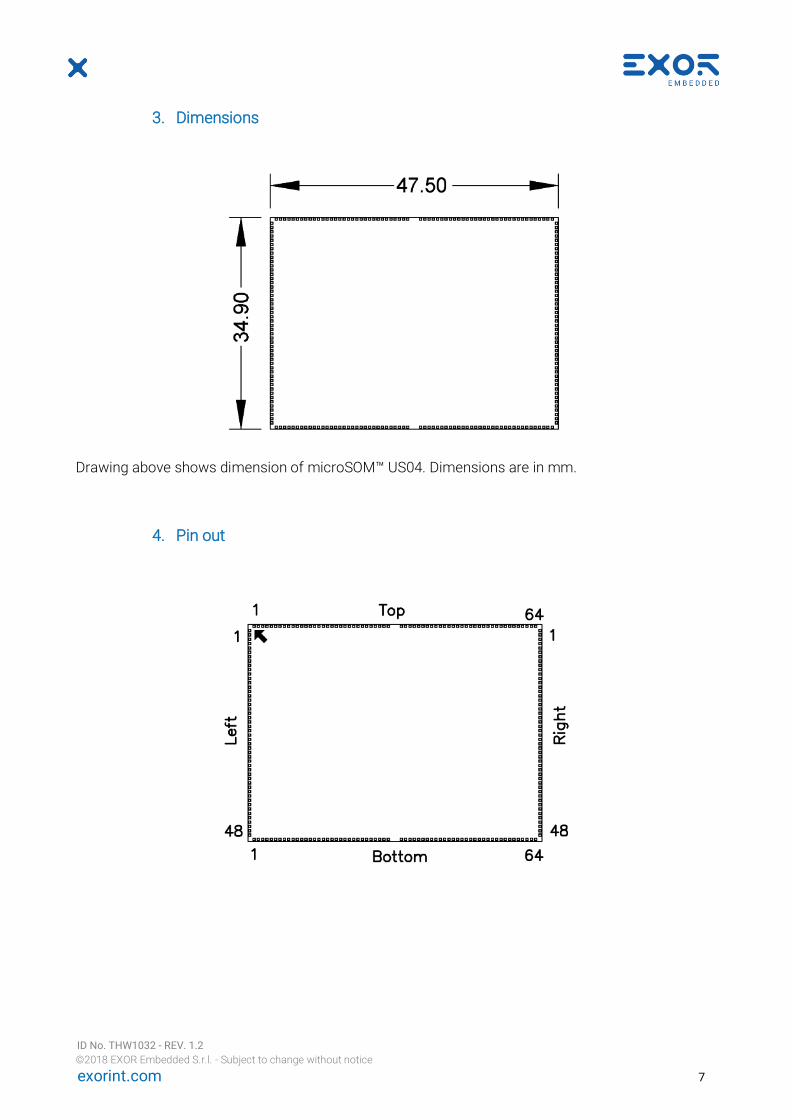
3. Dimensions
Drawing above shows dimension of microSOM™ US04. Dimensions are in mm.
4. Pin out
ID No. THW1032 - REV. 1.2
©2018 EXOR Embedded S.r.l. - Subject to change without notice
exorint.com 8
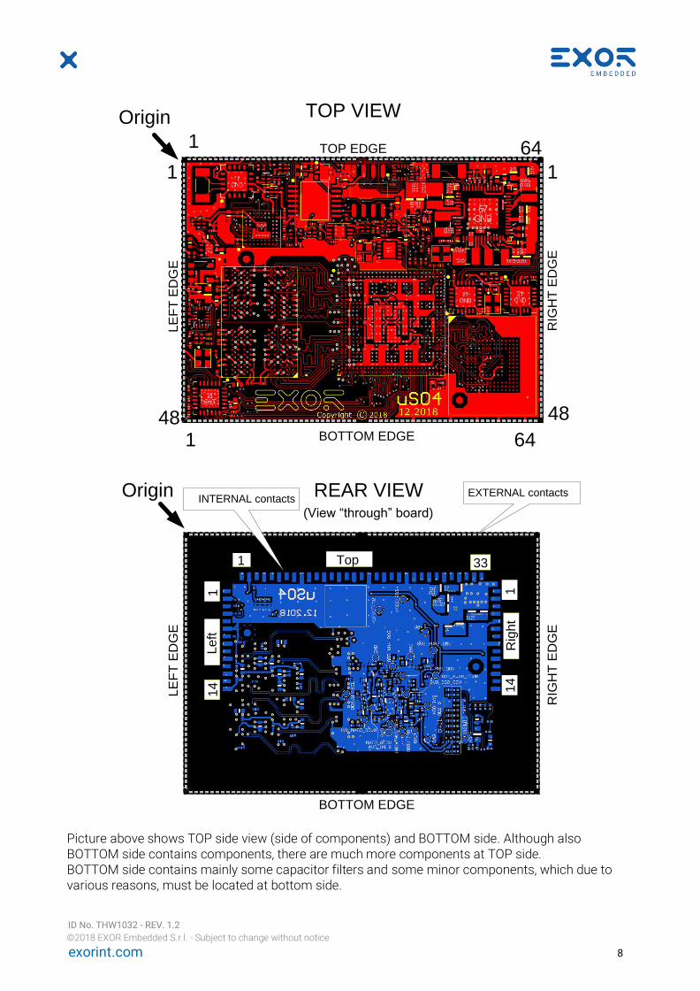
Picture above shows TOP side view (side of components) and BOTTOM side. Although also BOTTOM side contains components, there are much more components at TOP side. BOTTOM side contains mainly some capacitor filters and some minor components, which due to various reasons, must be located at bottom side.
TOP VIEW
REAR VIEW
Origin
1 64
641
4848
1 1
TOP EDGE
BOTTOM EDGE
LE
FT
ED
GE
RIG
HT
ED
GE
INTERNAL contactsEXTERNAL contacts
(View “through” board)
Origin
Top
Le
ft
Rig
ht
1
1 1
14 14
LE
FT
ED
GE
RIG
HT
ED
GE
BOTTOM EDGE
33

ID No. THW1032 - REV. 1.2
©2018 EXOR Embedded S.r.l. - Subject to change without notice
exorint.com 9
Note that carrier board for supporting microSOM™ US04 must have HOLE in central area. See below:
. microSOM™ US04 is built around:
• Four external (edge) ”connectors” (total 224 pins). • Three internal (edge) “connectors” (total 61 pins)
Really, these “connectors” are not true connectors, but simple soldering PADS, with pitch 0.7mm for external and 1mm for internal. Left and Right external “connector” are 48 pins, while Top and Bottom are 64 pins. Internal pads are: 14 (Left) + 33 (Top) +14 (Right) pads. All generic signals are direct LVCMOS/LVTTL (+3V3) compatible, except some special signals (RGMII1, RMII, LVDS, PCIe, USB…. what is described later). Next chapters show all pins, located at external and internal “connectors”. Most of signals are fixed by natural functions inside CPU. It means that these pins are already dedicated to i.MX8 M Mini local controllers and microSOM™ US04 is based at custom design, passed via PINMUX (tool for assigning pins to cores inside CPU). Note that user can change this default pin out for some pins, using PINMUX tool by NXP and one must be familiar with this, in case of changing. Also, some changes in firmware support in this can must be provided. Some signals (have name GPIO in column) are true GPIO, without some special using. These signals (GPIO) have various names in this tables, but these names are meaningless. These names are only inserted to show compatibility with some previous Exor CPU board (UN31). Customer shouldn’t pay attention to these names. Note also that some pins (GPIO) are coming from some other circuits from board (not CPU). Empty signals (empty rows) stand for NC (not connected) pins. These signals (pins) were used in some previous microSOM™ board, but here are NC.

ID No. THW1032 - REV. 1.2
©2018 EXOR Embedded S.r.l. - Subject to change without notice
exorint.com 10
4.1. Left connector external
Pin Signal Name Type CPU pin name Pin Comment 1 +3V3S Supply
Supply +3V3, 5% 2 +3V3S Supply 3 +3V3S Supply 4 +3V3S Supply 5 LVDSB_Tx0_P
LVDS Video OUT
CH B (Transmit)
Coming from on board
DSI to LVDS bridge
LVDS
Video OUT CHB
6 LVDSB_Tx0_N 7 LVDSB_Tx1_P 8 LVDSB_Tx1_N 9 LVDSB_Tx2_P
10 LVDSB_Tx2_N 11 LVDSB_Tx3_P 12 LVDSB_Tx3_N 13 LVDSB_Clk_P 14 LVDSB_Clk_N
15 16
17 GND 18 SPI1_CLK
SPI1
ECSPI1_SCLK D6 SPI channel 1
used as master (INT* can be
used as simple GPIO separately)
19 SPI1_CS0* ECSPI1_SS0 B6 20 SPI1_CS1* UART4_TXD F18 21 SPI1_SOMI ECSCPI1_MISO A7 22 SPI1_SIMO ECSPI1_MOSI B7
23 SPI1_INT* SAI5_RXFS AB15 24 GND 25 EN_SUPP_SD
SD Card Port 0 I2C extender
SD card AUX
signals 26 SD_CD* SD2_CD* AA26
27 SD_WP* SD2_WP* AA27 28 GND 29 SD_CLK
SD Card
SD2_CLK W23
SD card external
30 SD_CMD SD2_CMD W24 31 SD_D0 SD2_DATA0 AB23 32 SD_D1 SD2_DATA1 AB24 33 SD_D2 SD2_DATA2 V24
34 SD_D3 SD2_DATA3 V23 35 GPIO13 SAI1_TXD7 AF23 36 GND 37 USB1_DP
USB Port 1
Via local HUB USB port 1
from on board HUB
38 USB1_DM Via local HUB 39
40 USB1_DRVBUS Via local HUB 41 USB2_DP
USB Port 2
Via local HUB USB port 2
from on board HUB
42 USB2_DM Via local HUB 43 44 USB2_DRVBUS Via local HUB 45 USB_OC* Over
current Via local HUB
USB Driver. over current

ID No. THW1032 - REV. 1.2
©2018 EXOR Embedded S.r.l. - Subject to change without notice
exorint.com 11
46 +3V3S Supply Supply +3V3, 5% 47 +3V3S Supply
48 +3V3S Supply
4.2. Top connector external
Pin Name Type CPU pin name Pin Comment 1 LVDSA_Clk_N
LVDS Video OUT
CH A (Transmit)
Coming from on board
DSI to LVDS bridge
LVDS Video OUT CHA
2 LVDSA_Clk_P 3 LVDSA_Tx3_N 4 LVDSA_Tx3_P 5 LVDSA_Tx2_N 6 LVDSA_Tx2_P 7 LVDSA_Tx1_N 8 LVDSA_Tx1_P
9 LVDSA_Tx0_N 10 LVDSA_Tx0_P
11 GND 12 VBB Battery supply Ext. batt. 2V-5V input 13 SCL
I2C I2C1_SCL E9
I2C main channel 14 SDA I2C1_SDA F9 15 SYS_RST_OUT* (out from local chip) Reset OUT* (out**) 16 RES_IN* (inp. to supervisor). Reset IN* (in**)
17 POW_GOOD (out from local chip) POW_GOOD (out**) 18 PFAIL_IN* GPIO1_IO05 AF12 PFAIL_IN (in**) 19 AIN0
(Input to SPI/AD)
Five analog inputs 0---+1V8
20 AIN1 (Input to SPI/AD)
21 AIN2 (Input to SPI/AD) 22 AIN3 (Input to SPI/AD)
23 AIN4 (Input to SPI/AD) 24 AGND AGND 25 GND 25 EN_VDD
Video out control AUX
SPDIF_RX AG9 Video out AUX signals 27 PWM_DIMM SPDIF_TX AF9
28 EN_BLIGHT SPDIF_E_CL AF8
29 GPIO19
Port 5 of I2C ext. I2C Extender
PCA6408AHK with address 0x40
30 GPIO20 Port 4 of I2C ext.
31 GPIO21 Port 7 of I2C ext. 32 GPIO22 Port 6 of I2C ext. 33 GND 34 GPIO23
Port 3 of I2C ext. I2C Extender
PCA6408AHK with address 0x40
35 GPIO24 Port 2 of I2C ext. 36 GPIO25 Port 1 of I2C ext. 37 GPIO26 Port 0 of I2C ext. 38 GND 39 NAND_DQS
Nand port/ GPIO
NAND_DQS R22 Multifunctional NAND Port (NAND, eMMC, SD,
GPIO…) 40 NAND_ALE NAND_ALE N22 41 NAND_DATA_0 NAND_DATA_0 P23
ID No. THW1032 - REV. 1.2
©2018 EXOR Embedded S.r.l. - Subject to change without notice
exorint.com 12
42 NAND_DATA_1 NAND_DATA_1 K24 43 GND 44 NAND_DATA_2
Nand port/ GPIO
NAND_DATA_2 K23 Multifunctional NAND
Port (NAND, eMMC, SD, GPIO…)
45 NAND_DATA_3 NAND_DATA_3 N23 46 NAND_DATA_4 NAND_DATA_4 M26 47 NAND_DATA_5 NAND_DATA_5 L26 48 GND
49 NAND_DATA_6
Nand port/ GPIO
NAND_DATA_6 K26 Multifunctional NAND
Port (NAND, eMMC, SD, GPIO…)
50 NAND_DATA_7 NAND_DATA_7 N26 51 NAND_CLE NAND_CLE K27 52 NAND_CE3_B NAND_CE3_B L27 53 GND 54 NAND_CE2_B
Nand port/ GPIO
NAND_CE2_B M27 Multifunctional NAND
Port (NAND, eMMC, SD, GPIO…)
55 NAND_CE1_B NAND_CE1_B P27 56 NAND_CE0_B NAND_CE0_B N24 57 NAND_RDY_B NAND_RDY_B P26 58 GND 59 NAND_RE_B
Nand port/ GPIO
NAND_RE_B N27 Multifunctional NAND
Port (NAND, eMMC, SD, GPIO…)
60 NAND_WE_B NAND_WE_B R26
61 NAND_WP_B NAND_WP_B R27 62 63 GND 64 +3V3S Supply Supply +3V3, 5%
(**) These signals are system control I/O. SYS_RST_OUT* (RST_OUT*) is system reset, coming from circuits inside microSOM™ to RESET all peripherals inside microSOM™ US04 as wee; as at carrier board. Also, i.MX8M Mini can generate SYS_RST_OUT* (RST_OUT*) pulling pin RST_OUT*_L (GPIO located at pin SAI1_RXD6 pin AG19) to low. RES_IN* (RST_IN*) is (optionally) external RESET input signal (including reset KEY) POW_GOOD is control out from microSOM™ US04. Signal is generated high when all local supplies inside microSOM™ US04 finished power up procedure. User should use this signal to enable supply for I/O peripherals at carrier board. See in the rest of documents more description for this signal. PFAIL_IN* is optional PFAIL interrupt to inform microSOM™ US04 about Power Fail. Typical using is connecting this input to output of some comparator for main input (typically 24V).
4.3. Right connector external
Pin Name Type CPU pin name Pin
1 +3V3S Supply Supply +3V3, 5%
2 GND
3 RX1 UART1
SAI2_RXC AB22
UART1 of CPU 4 CTS1 SAI2_RXD0 AC24 5 RTS1 SAI2_TXFS AD23
ID No. THW1032 - REV. 1.2
©2018 EXOR Embedded S.r.l. - Subject to change without notice
exorint.com 13
6 TX1 SAI2_RXFS AC19 7 RX2
UART2
SAI3_TXFS AC6
UART2 of CPU 8 CTS2 SAI3_RXD AF7 9 RTS2 SAI3_RXC AG7 10 TX2 SAI3_TXC AG6 11 GND 12 RX3
UART3
ECSPI2_SCLK E6
UART4 of CPU 13 CTS3 ECSPI2_SS0 A6 14 RTS3 ECSPI2_MISO A8 15 TX3 ECSPI2_MOSI B8 16 CAN1_RX
CAN1 CAN1 from
SPI to CAN bridge 1 17 CAN1_TX 18 CAN2_RX
CAN2 CAN2 from
SPI to CAN bridge 2 19 CAN2_TX 20 GND 21 RGMII1_RXD0
RGMII CH1
ENET_RXD0 AE27
Only RGMII CH1 (+2V5 compatible)
22 RGMII1_RXD1 ENET_RXD1 AD27 23 RGMII1_RXD2 ENET_RXD2 AD26
24 RGMII1_RXD3 ENET_RXD3 AC26 25 GND 26 RGMII1_RXCLK RGMII
CH1 ENET_RXC AE26 Only RGMII CH1
(+2V5 compatible) 27 RGMII1_DV ENET_RX_CTL AF27 28 GND 29 RGMII1_TXD0
RGMII CH1
ENET_TXD0 AG26 Only RGMII CH1
(+2V5 compatible) 30 RGMII1_TXD1 ENET_TXD1 AF26
31 RGMII1_TXD2 ENET_TXD2 AG25 32 RGMII1_TXD3 ENET_TXD3 AF25
33 GND 34 RGMII1_TXCLK
RGMII CH1
ENET_TXC AG24 Only RGMII CH1 (+2V5 compatible)
INT optional +3V3 range 35 RGMII1_TXEN ENET_TX_CTL AF24 36 ETH_INT* SAI3_TXD AF6
37 GND
38 MDIO_CLK RGMII/RMII control
ENET MDC AC27 MD IO control
39 MDIO_DATA ENET_MDIO AB27 40 GND 41 RMII2_RXD0
RMII2 CH2 ENET_RXD0 AE27
Only RMII CH2 42 RMII2_RXD1 ENET_RXD1 AD27 43 1588_EV_IN
I2C2_SCL D10 1588 AUX signals
(optional) 44 1588_EV_OUT I2C2_SDA D9 45 GND 46 RMII2_Ref_CLK RMII2 CH2 ENET_TXD2 AG25 Only RMII CH2 47 +3V3S Supply
Supply +3V3, 5% 48 +3V3S Supply

ID No. THW1032 - REV. 1.2
©2018 EXOR Embedded S.r.l. - Subject to change without notice
exorint.com 14
4.4. Bottom connector external
Pin Name Type CPU pin name 1 +3V3S Supply
Supply +3V3, 5% 2 +3V3S Supply 3 SAI1_MCLK
SAI Audio or GPIO
SAI1_MCLK AB18
SAI Audio or GPIO 4 SAI1_TXFS SAI1_TXFS AB19 5 SAI1_TXC SAI1_TXC AC18 6 BUZZER Buzzer I2C4_SDA E13 Buzzer, PWM 7 GND 8 SAI1_TXD0
SAI Audio or GPIO
SAI1_TXD0 AG20
SAI Audio or GPIO
9 SAI1_TXD1 SAI1_TXD1 AF20
10 SAI1_TXD2 SAI1_TXD2 AG21 11 SAI1_TXD3 SAI1_TXD3 AF21 12 SAI1_RXFS SAI1_RXFS AG16 13 GPIO14
GPIO SAI5_RXD AF18
14 GPIO9 GPIO1_IO9 AF10
15 GPIO8 GPIO1_IO8 AG10
16 GND 17 GPIO7
GPIO
GPIO1_IO7 AF11
SAI Audio or GPIO
18 GPIO6 GPIO1_IO6 AG11 19 GPIO4 GPIO1_IO4 AG12 20 GPIO3 GPIO1_IO3 AF13 21 GPIO1 GPIO1_IO1 AF14 22 GPIO0 GPIO1_IO0 AG14
23 DL Two out used for ext. LED (Run & Error) 24 FAULT
25 SAI1_RXC
SAI Audio or GPIO
SAI1_RXC AF16
SAI Audio or GPIO 26 SAI1_RXD0 SAI1_RXD0 AG15 27 SAI1_RXD1 SAI1_RXD1 AF15 28 SAI1_RXD2 SAI1_RXD2 AG17
29 SAI1_RXD3 SAI1_RXD3 AF17 30 GND 31 SAI1_RXD4 SAI Audio or
GPIO SAI1_RXD4 AG18
SAI Audio or GPIO 32 SAI1_TXD4 SAI1_TXD4 AG22 33 34 GPIO18 GPIO Port 2 of I2C ext. I2C Extender (0X42)
35 GND 36 GPIO17
GPIO
Port 3 of I2C ext. I2C Extender PCA6408AHK
with address 0x42 37 GPIO16 Port 4 of I2C ext.
38 GPIO15 SD2_RESET_B AB25 39 40 I2S MCLK Audio I2S SAI5_MCLK AD15 I2S Audio
41 GND 42 SPI2_INT*
SPI2
SAI5_RXC AC15
SPI2 used as master (INT* can be used as
simple GPIO separately)
43 SPI2_SIMO UART1_TXD F13 44 SPI2_SOMI UART2_RXD F15 45 SPI2_CS1* SAI2_TXD0 AC22 46 SPI2_CS0* SAI3_RXFS AG8
47 SPI2_CLK UART1_RXD F14

ID No. THW1032 - REV. 1.2
©2018 EXOR Embedded S.r.l. - Subject to change without notice
exorint.com 15
48 GND 49 I2S BCLK
Audio I2S
SAI5_RXD2 AD13
I2S Audio 50 I2S RXD SAI5_RXD0 AD18 51 I2S SYNC SAI5_RXD1 AC14 52 I2S TXD SAI5_RXD3 AC13 53 GND 54 ETH_INT*
RMII2 CH2
SAI3_TXD AF6
Only RMII CH2 55 RMII2_TXEN ENET_TX_CTL AF24 56 RMII2_RX_ERR ENET_RXC AE26 57 GND 58 UART4L_RX
UART4 UART3_RXD E18 CPU UART3
(Only TX, RX) 59 UART4L_TX UART3_TXD D18 60 RMII2_TXD1
RMII2 CH2 ENET_TXD1 AF26
Only RMII CH2 61 RMII2_TXD0 ENET_TXD0 AG26 62 GND 63 RMII2_CRS_DV RMII2 CH2 ENET_RX_CTL AF27 Only RMII CH2 64 +3V3S Supply +3V3, 5%
4.5. Left connector internal
Pin Name Type CPU pin name Pin Comment 1 BOOT_MODE0X Control/Boot Control/ Boot Mode
2 PWM4 GPIO I2C4_SCL D13 GPIO (PWM opt.)
3 I2C_AUX_SCL GPIO I2C3_SCL E10 Aux I2C or GPIO
4 I2C_AUX_SDA GPIO I2C3_SDA F10 5
6 GND 7 JTAG_TCK JTAG_TCK F26
JTAG 8 JTAG_TMS JTAG_TMS F27 9 JTAG_TDO JTAG_TDO E26
10 JTAG_TDI JTAG_TDI E27 11 JTAG_RST* JTAG_RST* C27 12 GPIO11 GPIO SAI1_TXD5 AF22
Simple GPIO 13 GPIO12 GPIO SAI1_TXD6 AG23
14 GND
4.6. Top connector internal
Pin Name Type CPU (Pin name) 1 RES_IN* Control Control/ Boot Mode 2 USB_OTG_VBUS
USB OTG
USB1_VBUS F22 USB OTG 3 USB_OTG_DM USB1_DN A22
4 USB_OTG_DP USB1_DP B22

ID No. THW1032 - REV. 1.2
©2018 EXOR Embedded S.r.l. - Subject to change without notice
exorint.com 16
5 USB_OTG_ID GPIO1_IO10 AD10 6 7 8 9 GND
10 11
12 13 14 15 16 17
18 GND 19 20 21 22
23 GND
24 CSI_D3P
CSI_DSI (serial MIPI
Video in, 1,2,4 lines)
MIPI_CSI_D3P B18
CSI_DSI (serial MIPI
Video in, 1,2,4 lines)
25 CSI_D3N MIPI_CSI_D3N A18 26 CSI_D2P MIPI_CSI_D2P B17 27 CSI_D2N MIPI_CSI_D2N A17 28 CSI_D1P MIPI_CSI_D1P B15 29 CSI_D1N MIPI_CSI_D1N A15
30 CSI_D0P MIPI_CSI_D0P B14 31 CSI_D0n MIPI_CSI_D0N A14 32 CSI_CLKP MIPI_CSI_CLKP B16
33 CSI_CLKN MIPI_CSI_CLKN A16
4.7. Right connector internal
Pin Name Type CPU pin name Pin Comment 1 PCIE_TXP
PCIe PCIE_TX_P B20
PCIe (Tx line OUT) 2 PCIE_TXN PCIE_TX_N A20 3 PCIE_RXP
PCIe PCIE_RX_P B19
PCIe (Rx line IN) 4 PCIE_RXN PCIE_RX_N A19 5 GND
6 PCIE_CLKP PCIe
PCIE_CLK_P PCIe (CLK line) From local PCIe CLK gen. 7 PCIE_CLKN PCIE_CLK_N
8 GND 9
10 11 12 13 14
ID No. THW1032 - REV. 1.2
©2018 EXOR Embedded S.r.l. - Subject to change without notice
exorint.com 17
5. Description
microSOM™ US04 is built around SOC (System on chip) ARM 53 solo, dual, quad core, FBGA 486 pins, i.MX8M Mini (from NXP). Block diagram (next page) shows main microSOM™ US04 parts:
1) i.MX8M Mini CPU
2) AUX CIRCUITS (peripherals on board)
3) Power supplies
4) External and internal PADs (“connectors”) i.MX8M Mini is heart of microSOM™ US04, with up to four ARM A53 cores and provides (contains circuits for):
• Interface towards memory (LPDDR4)
• Interface towards eMMC
• USB interface (one OTG channel and one HOST connected to local HUB) • One Ethernet port (one MAC), which can be used for either RGMII or RMII PHY (*) • A lot of peripherals (UARTs, SD, I2C, Audio I2S, Video Out MIPI, Video In (CSI), SPI…) • High speed I/O (PCIe)
(*) Really there are two versions of microSOM™ US04, respecting Ethernet using.
• Version provided for using only with RGMII (10/100/1000Mb)
• Version provided for using only with RMII (10/100Mb) Reader will in the next chapters of document find differences between them. Note that also different pins are used for RMII or RGMII (due to compatibility with previous uSOM board - uS03)

ID No. THW1032 - REV. 1.2
©2018 EXOR Embedded S.r.l. - Subject to change without notice
exorint.com 18
z
RX
,TX
,RT
S,C
TS
SD
CA
RD
UA
RT
1
UA
RT
2
UA
RT
3
CA
N1
CA
N2
SP
I1
SP
I2
Au
dio
I 2C
6 s
ign
als
,CD
*,WP
*,En
_S
RX
,TX
,RT
S,C
TS
RX
,TX
,RT
S,C
TS
3 s
ign
als
+2
CS
*
3 s
ign
als
+2
CS
*
I 2S (5
sig
na
ls)
SC
L,S
DA
19
sig
na
ls
Re
se
t
ge
ne
rato
r
Po
w.G
oo
d
Fo
r RT
C o
nly
GP
IO
RS
T_O
UT
RS
T_IN
SD
2 p
ort
UA
RT
1
UA
RT
2
SP
I1
SP
I2
I 2S
2G
B
Lo
w P
ow
er
DD
RA
M4
eM
MC
RT
C
M4
1T
83
I 2C
Vb
b
SE
EP
RO
M
X2
4C
04
5 C
ha
ne
ls
12
bit A
/D
MC
P3
20
4
FR
AM
FM
25
L5
12
SP
I1
24M
hz
An
alo
g
CH
0-C
H4
+5
VL
oa
d s
witc
h
AUX PADS
(Internal)
Vb
b
(2-5
)V b
att.
US
B1
US
B2
EXTERNAL PADS
RG
MII1
RM
II2
Po
we
r su
pp
ly b
lock
USB2
PC
Ie T
x
GP
IO
XT
AL
_I
XT
AL_
O
SP
I1
eM
MC
LP
DD
R4
co
ntro
ller
Co
ntro
l
32
bits
Da
ta
An
alo
g C
H0
-CH
4
IMX8m Mini
VD
D A
RM
0V
9
US
B H
UB
US
B 2
42
2
On
ly R
MG
II ch
an
ne
l (10M
b/1
00
Mb/1
Gb
)
On
ly R
MII c
ha
nn
el (1
0M
b,1
00M
b)
JT
AG
US
B1
MIP
I_C
SI
(2 G
PIO
+ 1
PW
M)
5 s
ign
als
2 s
ign
als
10
sig
na
ls
(1,2
,or 4
ch
an
ne
ls)
On board
Periph.
32
/
76
8K
hz
VID
EO
_O
UT
VID
EO
_O
UT
_M
IPI D
SI
CH
_A
DC
/DC
1V
35
+3V
3S
+3
V3
S
+3
V3
S
+3V
3S
DC
/DC
0V
8
DC
/DC
0V
9
DC
/DC
0V
9
DC
/DC
1V
8
+3
V3
S
PO
R*
PO
W_
ON
*
ST
DB
Y R
EQ
SC
L
SD
A
Co
ntro
l
BD
71
48
7
+3
V3
S
RS
T*
Po
r.*
On
ly o
ne
MA
C
(Ca
n b
e u
se
d
eith
er R
GM
II
or R
MII)
VD
D S
OC
0V
8
VD
D D
RA
M
& P
U 0
V9
0V
9
VD
D 1
V8
DC
/DC
1V
1N
VC
C D
RA
M
1V
1
NV
CC
SN
VS
1V
8
VD
D S
NV
S
0V
8
VD
D P
HY
0V
9
VD
D P
HY
1V
2
VD
DA
1V
8
NV
CC
_S
D2
LD
O
+3
V3
SL
oa
d s
witc
h
TP
S2
29
15
CY
PF
T
+3
V3 R
TC
_R
ST
*
PM
IC_
INT
MIP
I
DS
I to
LV
DS
brid
ge
VID
EO
_O
UT
CH
_B
SP
I to
CA
N
brid
ge
SP
I to
CA
N
brid
ge
SP
I2
SP
I2
I 2C1
AU
X v
ide
o
co
ntro
lA
UX
Vid
eo
ou
t co
ntro
l.E
n_
Vd
d, E
n_
BL,D
imm
UA
RT
4R
X,T
XU
AR
T3
(GP
IO)
NA
ND
Pa
r. BU
S
GP
IO fro
m C
PU
NA
ND
Pa
r. BU
S
(OT
G p
ort)2
5M
hz
En
Du
al P
CIe
CL
K o
sc.
PC
Ie R
x
PC
Ie C
lk
Fiv
e a
na
log
inp
uts
CH
0-C
H4
Bu
zze
r
Du
al 8
bits
I 2C e
xte
nd
.
RX
,TX
RX
,TX
13
sig
na
ls
Bu
zze
r
UA
RT
4
I 2C A
UX
GP
IO (I 2C
)
Po
we
r go
od
11
sig
na
ls
I 2CI 2C
SA
I (Au
dio
)/GP
IOS
AI/ G
PIO
from
exte
nd
ers
14
sig
na
ls
ID No. THW1032 - REV. 1.2
©2018 EXOR Embedded S.r.l. - Subject to change without notice
exorint.com 19
5.1. i.MX8M Mini
5.1.1. Quad core ARM A53 CPU
microSOM™ US04 is based at i.MX8M Mini, Quad/Dual/Single ARM A53 core, located in SOC, which operates at speed up to 1.6 GHz for industrial version of CPU.
5.1.2. Embedded memory controller (LPDDRAM4)
i.MX8M Mini includes embedded memory controller with support for various memory types. In microSOM™ US04 is used 2GB LPDDRAM4 (1500 MHz clock).
5.1.3. eMMC e SD
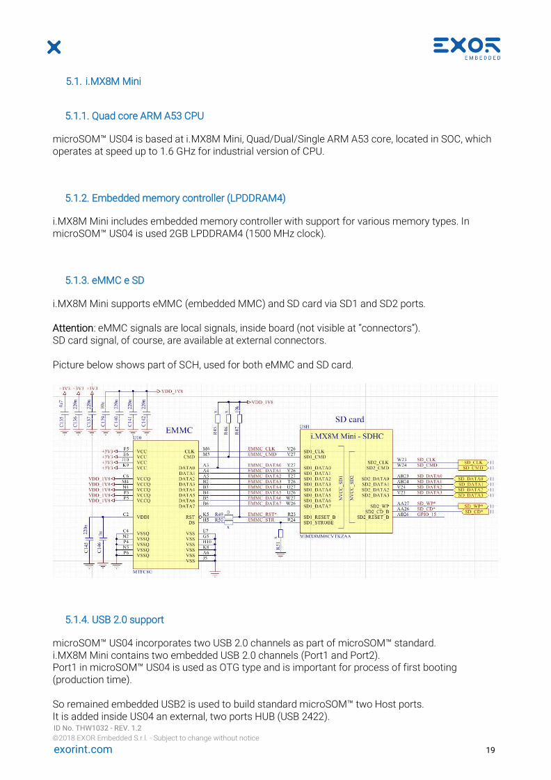
i.MX8M Mini supports eMMC (embedded MMC) and SD card via SD1 and SD2 ports. Attention: eMMC signals are local signals, inside board (not visible at “connectors”). SD card signal, of course, are available at external connectors. Picture below shows part of SCH, used for both eMMC and SD card.
5.1.4. USB 2.0 support
microSOM™ US04 incorporates two USB 2.0 channels as part of microSOM™ standard. i.MX8M Mini contains two embedded USB 2.0 channels (Port1 and Port2). Port1 in microSOM™ US04 is used as OTG type and is important for process of first booting (production time). So remained embedded USB2 is used to build standard microSOM™ two Host ports. It is added inside US04 an external, two ports HUB (USB 2422).

ID No. THW1032 - REV. 1.2
©2018 EXOR Embedded S.r.l. - Subject to change without notice
exorint.com 20
This way, user can see two USB channels (Note that is possible only HOST mode using for USB2 in microSOM™ US04.
5.1.5. USB 2.0 OTG support
It is noted before that microSOM™ US04 contains also additional USB OTG port. This port is connected to embedded Port 1 of i.MX8 Mini. This USB OTG port is not part of standard microSOM™ signals (for example US01 and US02 have not this port), but port is inserted starting from US03 as part of additional signals as one mandatory features for NXP CPU. In addition, this port can be used in normal “run” mode as standard OTG or Device channel.
5.1.6. UART1, UART2, UART3 and UART4
Three embedded interfaces (UART1, UART2 and UART4) from i.MX8M Mini are used for system UART1, UART2 and UART3 channels with using all four serial lines (RX, TX, CTS, RTS). In addition, microSOM™ US04, can use also additional UART with only TX and RX (UART 3). This the fourth UART is not mandatory and is not part of USOM standard but can be used in case of some special need or as simple GPIO. Note also that CPU UART3 is mapped as system UART4 and CPU UART4 is mapped as system UART3.
Signal name Signal Name (CPU) Pin
RX1 SAI2_RXC AB22 CTS1 SAI2_RXD0 AC24 RTS1 SAI2_TXFS AD23 TX1 SAI2_RXFS AC19 RX2 SAI3_TXFS AC6
CTS2 SAI3_RXD AF7
ID No. THW1032 - REV. 1.2
©2018 EXOR Embedded S.r.l. - Subject to change without notice
exorint.com 21
RTS2 SAI3_RXC AG7 TX2 SAI3_TXC AG6 RX3 ECSPI2_SCLK E6
CTS3 ECSPI2_SS0 A6 RTS3 ECSPI2_MISO A8 TX3 ECSPI2_MOSI B8 RX4 UART3_RXD E18
TX4 UART3_TXD D18
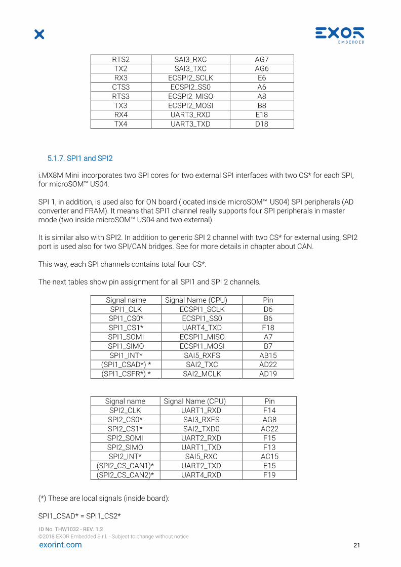
5.1.7. SPI1 and SPI2
i.MX8M Mini incorporates two SPI cores for two external SPI interfaces with two CS* for each SPI, for microSOM™ US04. SPI 1, in addition, is used also for ON board (located inside microSOM™ US04) SPI peripherals (AD converter and FRAM). It means that SPI1 channel really supports four SPI peripherals in master mode (two inside microSOM™ US04 and two external). It is similar also with SPI2. In addition to generic SPI 2 channel with two CS* for external using, SPI2 port is used also for two SPI/CAN bridges. See for more details in chapter about CAN. This way, each SPI channels contains total four CS*. The next tables show pin assignment for all SPI1 and SPI 2 channels.
Signal name Signal Name (CPU) Pin
SPI1_CLK ECSPI1_SCLK D6 SPI1_CS0* ECSPI1_SS0 B6 SPI1_CS1* UART4_TXD F18 SPI1_SOMI ECSPI1_MISO A7
SPI1_SIMO ECSPI1_MOSI B7
SPI1_INT* SAI5_RXFS AB15 (SPI1_CSAD*) * SAI2_TXC AD22 (SPI1_CSFR*) * SAI2_MCLK AD19
Signal name Signal Name (CPU) Pin SPI2_CLK UART1_RXD F14 SPI2_CS0* SAI3_RXFS AG8
SPI2_CS1* SAI2_TXD0 AC22 SPI2_SOMI UART2_RXD F15 SPI2_SIMO UART1_TXD F13 SPI2_INT* SAI5_RXC AC15
(SPI2_CS_CAN1)* UART2_TXD E15 (SPI2_CS_CAN2)* UART4_RXD F19
(*) These are local signals (inside board): SPI1_CSAD* = SPI1_CS2*

ID No. THW1032 - REV. 1.2
©2018 EXOR Embedded S.r.l. - Subject to change without notice
exorint.com 22
SPI1_CSFR* = SPI1_CS3* SPI2_CS_CAN1* = SPI2_CS2* SPI2_CS_CAN2* = SPI2_CS3* SPI1_INT* and SPI2_INT* are not mandatory signals for SPI. Can be used as GPIO.
5.1.8. Audio OUT
microSOM™ US04 contains one Audio OUT I2S channel, compatible with uSOM standard. The last signal presented in table below is not mandatory. For 4-bit I2S can be externally generated.
Signal name Signal Name (CPU) Pin I2S BCLK SAI5_RXD2 AD13 I2S RXD SAI5_RXD0 AD18
I2S SYNC SAI5_RXD1 AC14 I2S TXD SAI5_RXD3 AC13
I2S MCLK SAI5_MCLK AD15
5.1.9. I2C
ARM CPU inside i.MX8M Mini contains total four I2C ports, but only two are used. It is used I2C1 system I2C controller in microSOM™ US04. It is main I2C channel, used in microSOM™ standard for nearly all I2C operations.
Signal name Signal Name (CPU) Pin SCL I2C1_SCL E9 SDA I2C1_SDA F9
microSOM™ US04 (like US03) supports also one addition (AUX) I2C controller. (I2C3 in IMX8M Mini). Using this channel as I2C is not mandatory, but can be useful, to separate from main I2C. In each case, pins can be used as GPIO.
Signal name Signal Name (CPU) Pin SCL_AUX I2C3_SCL E10 SDA_AUX I2C3_SDA F10
5.1.10. Video out
ARM CPU inside i.MX8M Mini contains MIPI DSI interface as main video out. This format is not compatible with previous EXOR’s boards (mainly US030). It was reason to incorporate MIPS DSI to LVDS dual channel bridge SN65DS184ZQRB

ID No. THW1032 - REV. 1.2
©2018 EXOR Embedded S.r.l. - Subject to change without notice
exorint.com 23
In addition to standard Data signals, video controller part is followed with some additional control signals:
Signal name Signal Name (CPU) Pin EN_VDD (*) SPDIF_RX AG9
PWM_DIMM (**) SPDIF_TX AF9 EN_BLIGHT (***) SPDIF_E_CL AF8
EN_VID_BRIDGE Port 1 of I2C ext. Ext. with
address 0X42 VIDEO_INT GPIO1_IO15 AB9
(*) Signal used as enable display supply for external supply. (**) Signal used as PWM adjustment signal for backlight (dimming). (***) Signal used as backlight enable signal Last two signals are local signals for SN65DS184ZQRB MIPI to LVDS bridge. Drawing at next page shows connecting MIPS DSI controller inside CPU to Video bridge.

ID No. THW1032 - REV. 1.2
©2018 EXOR Embedded S.r.l. - Subject to change without notice
exorint.com 24
5.1.11. Video input serial (MIPI CSI)
microSOM™ US04 supports also MIPI (CSI) (serial video input port) via two 1, 2, 4 lines interface. Signals of CSI interface are located at internal interface pins. Picture bellows shows connection MIPI_CSI signals to CPU.
5.1.12. Ethernet
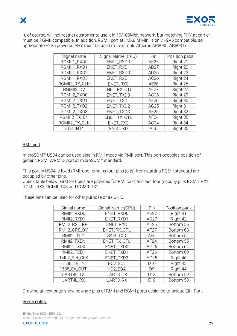
microSOM™ US04 has possibility to support two types of Ethernet connectivity (ports), but no contemporary. These ports occupy different external pads. Selection of different pads for supporting one or other Ethernet type is directed by fact that similar approach is used also for US03 and US04 has high level of compatibility’ with US03. In rest of document these ports will be named RGMII (Ethernet port 1) and RMII (Ethernet port 2). Note that selection of ports is not simple (changing some jumpers or similar), but really customer needs in advance to select one of two versions of microSOM™ US04 (version RGMII or version RMII). These versions are using different pins and even supplies. It means that user can select to build only one port: (RGMII) for 10/100/1000Mb or (RMII for 10/100Mb). Have a mind that user should make right selection. 10/100Mb PHY solution offers lower cost PHY, but 10/100/1000Mb PHY, of course, better performance. User can build only one Ethernet port, because these ports use the same MAC inside microSOM. In case that user needs one second Ethernet port (second MAC), good solution is to use PCIe based PHY at carrier board (for example Intel I210). RGMII port This port occupies position of generic RGMII1 port at microSOM™ standard (Right side). Starting microSOM™ standard provides that Ethernet port is generic (can be used either RGMII or RMII), but due to i.MX8M Mini restriction, we can use ONLY as RGMII port. Attention: This port (if used, because MAC is common) works only in RGMII mode.
ID No. THW1032 - REV. 1.2
©2018 EXOR Embedded S.r.l. - Subject to change without notice
exorint.com 25
It, of course, will not restrict customer to use it in 10/100Mbit network, but matching PHY at carrier must be RGMII compatible. In addition, RGMII port at i.MX8 M Mini is only +2V5 compatible, so appropriate +2V5 powered PHY must be used (for example Atheros AR8035, AR8031).
Signal name Signal Name (CPU) Pin Position pads RGMII1_RXD0 ENET_RXD0 AE27 Right 21 RGMII1_RXD1 ENET_RXD1 AD27 Right 22
RGMII1_RXD2 ENET_RXD0 AD26 Right 23
RGMII1_RXD3 ENET_RXD1 AC26 Right 24
RGMII2_RX_CLK ENET_RXC AE26 Right 26
RGMII2_DV ENET_RX_CTL AF27 Right 27 RGMII2_TXD0 ENET_TXD0 AG26 Right 29
RGMII2_TXD1 ENET_TXD1 AF26 Right 30
RGMII2_TXD2 ENET_TXD2 AG25 Right 31
RGMII2_TXD3 ENET_TXD3 AF25 Right 32
RGMII2_TX_EN ENET_TX_CTL AF24 Right 35
RGMII2_TX_CLK ENET_TXC AG24 Right 34
ETH_INT* SAI3_TXD AF6 Right 36
RMII port microSOM™ US04 can be used also in RMII mode via RMII port. This port occupies position of generic RGMII2/RMII2 port at microSOM™ standard. This port in US04 is fixed (RMII), so remains four pins (bits) from starting RGMII standard are occupied by other pins. Check table below. First 8+1 pins are provided for RMII port and last four (occupy pins RGMII_RX2, RGMII_RX3, RGMII_TX3 and RGMII_TX2. These pins can be used for other purpose or as GPIO.
Signal name Signal Name (CPU) Pin Position pads RMII2_RXD0 ENET_RXD0 AE27 Right 41 RMII2_RXD1 ENET_RXD1 AD27 Right 42
RMII2_RX_ERR ENET_RXC AE26 Bottom 56
RMII2_CRS_DV ENET_RX_CTL AF27 Bottom 63
RMII2_INT* SAI3_TXD AF6 Bottom 54
RMII2_TXEN ENET_TX_CTL AF24 Bottom 55 RMII2_TXD0 ENET_TXD0 AG26 Bottom 61
RMII2_TXD1 ENET_TXD1 AF26 Bottom 60
RMII2_Ref_CLK ENET_TXD2 AG25 Right 46
1588_EV_IN I2C2_SCL D10 Right 43
1588_EV_OUT I2C2_SDA D9 Right 44
UART4L_TX UART3_TX D18 Bottom 59
UART4L_RX UART3_RX E18 Bottom 58
Drawing at next page show how are pins of RMII and RGMII ports assigned to unique Eth. Port. Some notes:

ID No. THW1032 - REV. 1.2
©2018 EXOR Embedded S.r.l. - Subject to change without notice
exorint.com 26
• MDC and MDIO are really common for RGMII1 port and RMII2 ports (+3V3 compatibility)
• RGMII1_INT* is not part of standard, but can be used (+3V3 compatibility)
5.1.14. PCIe port
PCI clock is generated by local clock generator and its copy is routed as external PCIE_CLK pair.
ID No. THW1032 - REV. 1.2
©2018 EXOR Embedded S.r.l. - Subject to change without notice
exorint.com 27
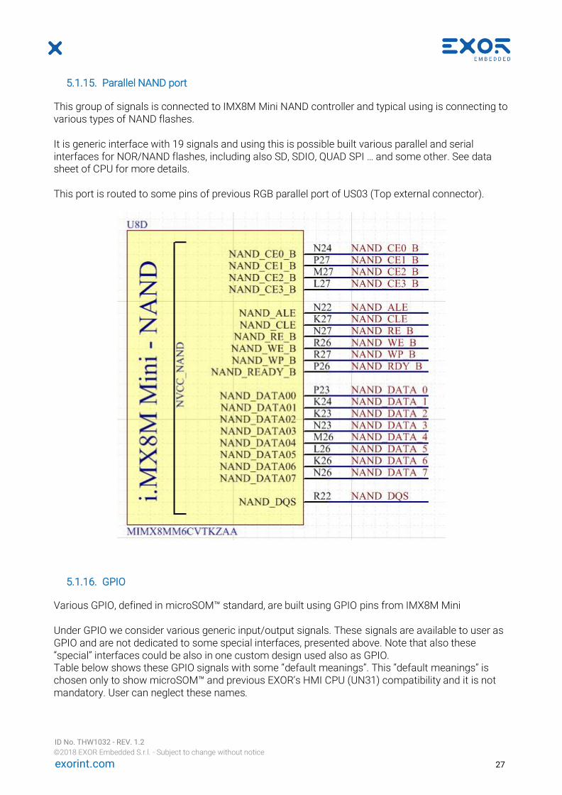
5.1.15. Parallel NAND port
This group of signals is connected to IMX8M Mini NAND controller and typical using is connecting to various types of NAND flashes. It is generic interface with 19 signals and using this is possible built various parallel and serial interfaces for NOR/NAND flashes, including also SD, SDIO, QUAD SPI … and some other. See data sheet of CPU for more details. This port is routed to some pins of previous RGB parallel port of US03 (Top external connector).
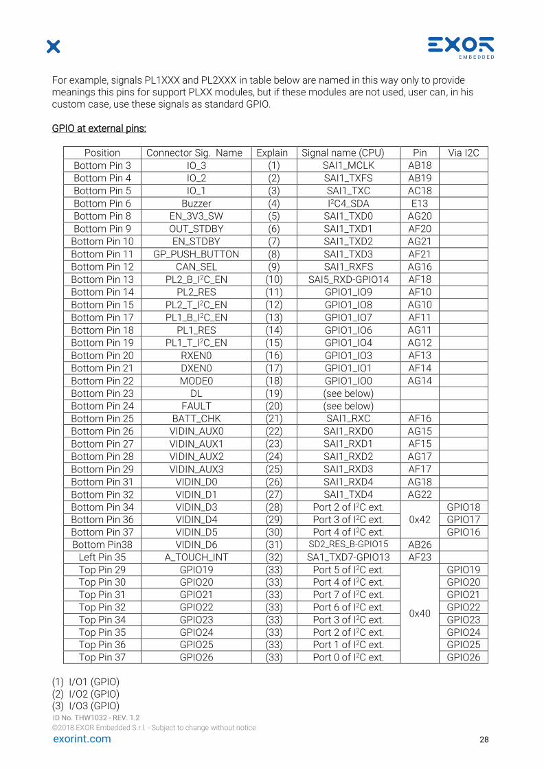
5.1.16. GPIO
Various GPIO, defined in microSOM™ standard, are built using GPIO pins from IMX8M Mini Under GPIO we consider various generic input/output signals. These signals are available to user as GPIO and are not dedicated to some special interfaces, presented above. Note that also these “special” interfaces could be also in one custom design used also as GPIO. Table below shows these GPIO signals with some “default meanings”. This “default meanings” is chosen only to show microSOM™ and previous EXOR’s HMI CPU (UN31) compatibility and it is not mandatory. User can neglect these names.
ID No. THW1032 - REV. 1.2
©2018 EXOR Embedded S.r.l. - Subject to change without notice
exorint.com 28
For example, signals PL1XXX and PL2XXX in table below are named in this way only to provide meanings this pins for support PLXX modules, but if these modules are not used, user can, in his custom case, use these signals as standard GPIO. GPIO at external pins:
Position Connector Sig. Name Explain Signal name (CPU) Pin Via I2C
Bottom Pin 3 IO_3 (1) SAI1_MCLK AB18
Bottom Pin 4 IO_2 (2) SAI1_TXFS AB19 Bottom Pin 5 IO_1 (3) SAI1_TXC AC18
Bottom Pin 6 Buzzer (4) I2C4_SDA E13 Bottom Pin 8 EN_3V3_SW (5) SAI1_TXD0 AG20
Bottom Pin 9 OUT_STDBY (6) SAI1_TXD1 AF20 Bottom Pin 10 EN_STDBY (7) SAI1_TXD2 AG21
Bottom Pin 11 GP_PUSH_BUTTON (8) SAI1_TXD3 AF21 Bottom Pin 12 CAN_SEL (9) SAI1_RXFS AG16
Bottom Pin 13 PL2_B_I2C_EN (10) SAI5_RXD-GPIO14 AF18 Bottom Pin 14 PL2_RES (11) GPIO1_IO9 AF10
Bottom Pin 15 PL2_T_I2C_EN (12) GPIO1_IO8 AG10 Bottom Pin 17 PL1_B_I2C_EN (13) GPIO1_IO7 AF11
Bottom Pin 18 PL1_RES (14) GPIO1_IO6 AG11 Bottom Pin 19 PL1_T_I2C_EN (15) GPIO1_IO4 AG12
Bottom Pin 20 RXEN0 (16) GPIO1_IO3 AF13 Bottom Pin 21 DXEN0 (17) GPIO1_IO1 AF14
Bottom Pin 22 MODE0 (18) GPIO1_IO0 AG14
Bottom Pin 23 DL (19) (see below) Bottom Pin 24 FAULT (20) (see below)
Bottom Pin 25 BATT_CHK (21) SAI1_RXC AF16 Bottom Pin 26 VIDIN_AUX0 (22) SAI1_RXD0 AG15
Bottom Pin 27 VIDIN_AUX1 (23) SAI1_RXD1 AF15
Bottom Pin 28 VIDIN_AUX2 (24) SAI1_RXD2 AG17
Bottom Pin 29 VIDIN_AUX3 (25) SAI1_RXD3 AF17
Bottom Pin 31 VIDIN_D0 (26) SAI1_RXD4 AG18
Bottom Pin 32 VIDIN_D1 (27) SAI1_TXD4 AG22
Bottom Pin 34 VIDIN_D3 (28) Port 2 of I2C ext. 0x42
GPIO18 Bottom Pin 36 VIDIN_D4 (29) Port 3 of I2C ext. GPIO17 Bottom Pin 37 VIDIN_D5 (30) Port 4 of I2C ext. GPIO16 Bottom Pin38 VIDIN_D6 (31) SD2_RES_B-GPIO15 AB26
Left Pin 35 A_TOUCH_INT (32) SA1_TXD7-GPIO13 AF23 Top Pin 29 GPIO19 (33) Port 5 of I2C ext.
0x40
GPIO19 Top Pin 30 GPIO20 (33) Port 4 of I2C ext. GPIO20 Top Pin 31 GPIO21 (33) Port 7 of I2C ext. GPIO21 Top Pin 32 GPIO22 (33) Port 6 of I2C ext. GPIO22 Top Pin 34 GPIO23 (33) Port 3 of I2C ext. GPIO23
Top Pin 35 GPIO24 (33) Port 2 of I2C ext. GPIO24 Top Pin 36 GPIO25 (33) Port 1 of I2C ext. GPIO25 Top Pin 37 GPIO26 (33) Port 0 of I2C ext. GPIO26
(1) I/O1 (GPIO) (2) I/O2 (GPIO) (3) I/O3 (GPIO)
ID No. THW1032 - REV. 1.2
©2018 EXOR Embedded S.r.l. - Subject to change without notice
exorint.com 29
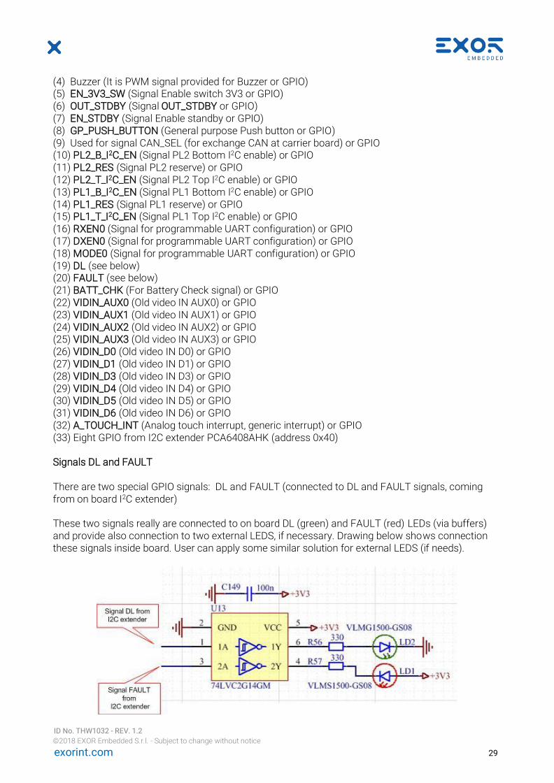
(4) Buzzer (It is PWM signal provided for Buzzer or GPIO) (5) EN_3V3_SW (Signal Enable switch 3V3 or GPIO) (6) OUT_STDBY (Signal OUT_STDBY or GPIO) (7) EN_STDBY (Signal Enable standby or GPIO) (8) GP_PUSH_BUTTON (General purpose Push button or GPIO) (9) Used for signal CAN_SEL (for exchange CAN at carrier board) or GPIO (10) PL2_B_I2C_EN (Signal PL2 Bottom I2C enable) or GPIO (11) PL2_RES (Signal PL2 reserve) or GPIO (12) PL2_T_I2C_EN (Signal PL2 Top I2C enable) or GPIO (13) PL1_B_I2C_EN (Signal PL1 Bottom I2C enable) or GPIO (14) PL1_RES (Signal PL1 reserve) or GPIO (15) PL1_T_I2C_EN (Signal PL1 Top I2C enable) or GPIO (16) RXEN0 (Signal for programmable UART configuration) or GPIO (17) DXEN0 (Signal for programmable UART configuration) or GPIO (18) MODE0 (Signal for programmable UART configuration) or GPIO (19) DL (see below) (20) FAULT (see below) (21) BATT_CHK (For Battery Check signal) or GPIO (22) VIDIN_AUX0 (Old video IN AUX0) or GPIO (23) VIDIN_AUX1 (Old video IN AUX1) or GPIO (24) VIDIN_AUX2 (Old video IN AUX2) or GPIO (25) VIDIN_AUX3 (Old video IN AUX3) or GPIO (26) VIDIN_D0 (Old video IN D0) or GPIO (27) VIDIN_D1 (Old video IN D1) or GPIO (28) VIDIN_D3 (Old video IN D3) or GPIO (29) VIDIN_D4 (Old video IN D4) or GPIO (30) VIDIN_D5 (Old video IN D5) or GPIO (31) VIDIN_D6 (Old video IN D6) or GPIO (32) A_TOUCH_INT (Analog touch interrupt, generic interrupt) or GPIO (33) Eight GPIO from I2C extender PCA6408AHK (address 0x40) Signals DL and FAULT There are two special GPIO signals: DL and FAULT (connected to DL and FAULT signals, coming from on board I2C extender) These two signals really are connected to on board DL (green) and FAULT (red) LEDs (via buffers) and provide also connection to two external LEDS, if necessary. Drawing below shows connection these signals inside board. User can apply some similar solution for external LEDS (if needs).

ID No. THW1032 - REV. 1.2
©2018 EXOR Embedded S.r.l. - Subject to change without notice
exorint.com 30
Typical using for FAULT is presenting some ERROR condition and for DL (Diagnostic Led) is presetting some diagnostic information (for example blinking various frequencies) for various events. GPIO at internal pins: There are also some GPIO at internal PADS. Table below shows these pins
Position Signal Name Explain Signal name (CPU) Pin Left Pin 2 PWM4 (1) I2C4_SCL E10
Left Pin 12 I/O_6 (2) SAI1_TXD5-GPIO11 AF22
Left Pin 13 I/O_7 (3) SAI1_TXD6-GPIO12 AG23 (1) PWM4 Can be used as PWM signal or simple GPIO (2) I/O6 (simple GPIO) (3) I/O7 (simple GPIO)
5.1.17. GPIO bank from CPU
In previous chapter 5.1.16 are presented all GPIO signals available for customer. These signals are coming from various CPU blocks, as well as two I2C extenders. This chapter present one special group GPIO signals. Really these signals are part of CPU special bank named GPIO1. These signals in CPU have not some special function and are provided for generic using. Some of these signals are used as simple GPIO (these signals already explained in chapter 5.1.16) and other are used for some local, on board functions. Picture at next page show this CPU bank and these signals. Most of them are real GPIO. Some of them are used for USB functions or some local interrupts.
ID No. THW1032 - REV. 1.2
©2018 EXOR Embedded S.r.l. - Subject to change without notice
exorint.com 31
5.2. AUX Circuits
microSOM™ US04 contains some additional circuits.
5.2.1. RTC
For microSOM™ US04 for RTC purpose is used M41T83 RTC chip, although IMX8M Mini has own RTC. Solution with M41T83 RTC is much better in power OFF (battery) mode. Chip is supplied (standby mode) with Vbb (Vbattery). Vbb can be in range 2-5.5 V. Consumption in standby mode is about 400 nA.
5.2.2. FRAM
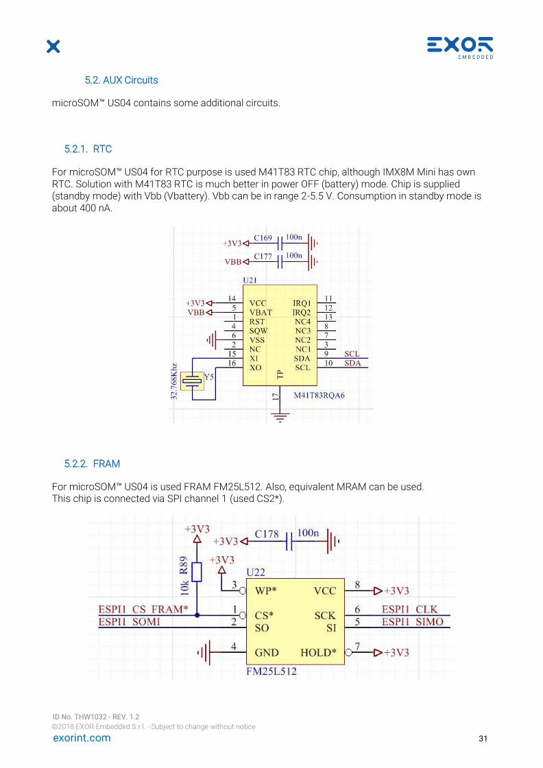
For microSOM™ US04 is used FRAM FM25L512. Also, equivalent MRAM can be used. This chip is connected via SPI channel 1 (used CS2*).

ID No. THW1032 - REV. 1.2
©2018 EXOR Embedded S.r.l. - Subject to change without notice
exorint.com 32
5.2.3. SEEPROM
microSOM™ US04 contains one standard I2C SEEPROM (X24C04) with address 0x50.
5.2.4. SPI A/D
microSOM™ US04 contains also five channels SPI 12 bits A/D converter. SPI converter is connected via SPI 1 channel (used CS3* of SPI channel). Analog input range is 0-1.8V. Control signal SEL_A3A4 for selection A3 or A4 is coming from I2C extender.
5.2.5. CAN
Due to lack of natural CAN controller inside CPU core, in microSOM™ US04 are used two SPI/CAN bridges. It is used SP2 channel with two additional CS*. See for more details in chapter for SPI2 description (5.1.7).
ID No. THW1032 - REV. 1.2
©2018 EXOR Embedded S.r.l. - Subject to change without notice
exorint.com 33
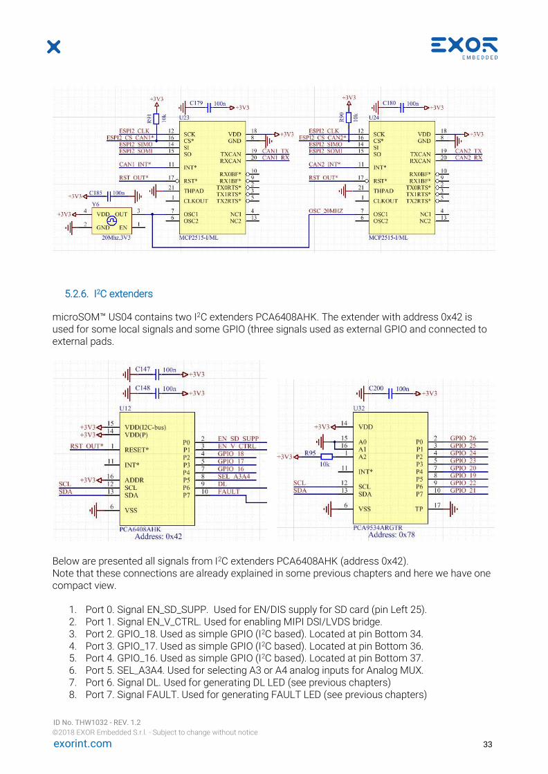
5.2.6. I2C extenders
microSOM™ US04 contains two I2C extenders PCA6408AHK. The extender with address 0x42 is used for some local signals and some GPIO (three signals used as external GPIO and connected to external pads.
Below are presented all signals from I2C extenders PCA6408AHK (address 0x42). Note that these connections are already explained in some previous chapters and here we have one compact view.
1. Port 0. Signal EN_SD_SUPP. Used for EN/DIS supply for SD card (pin Left 25). 2. Port 1. Signal EN_V_CTRL. Used for enabling MIPI DSI/LVDS bridge. 3. Port 2. GPIO_18. Used as simple GPIO (I2C based). Located at pin Bottom 34. 4. Port 3. GPIO_17. Used as simple GPIO (I2C based). Located at pin Bottom 36. 5. Port 4. GPIO_16. Used as simple GPIO (I2C based). Located at pin Bottom 37. 6. Port 5. SEL_A3A4. Used for selecting A3 or A4 analog inputs for Analog MUX. 7. Port 6. Signal DL. Used for generating DL LED (see previous chapters) 8. Port 7. Signal FAULT. Used for generating FAULT LED (see previous chapters)
ID No. THW1032 - REV. 1.2
©2018 EXOR Embedded S.r.l. - Subject to change without notice
exorint.com 34
The second extender (with address 0x78) is used for eight simple GPIO (I2C based).
1. Port 0. Signal GPIO_26. Connected to Top 37 2. Port 1. Signal GPIO_25. Connected to Top 36 3. Port 2. Signal GPIO_24. Connected to Top 35 4. Port 3. Signal GPIO_23. Connected to Top 34 5. Port 4. Signal GPIO_20. Connected to Top 30 6. Port 5. Signal GPIO_19. Connected to Top 29 7. Port 6. Signal GPIO_22. Connected to Top 32 8. Port 7. Signal GPIO_21. Connected to Top 31
5.3. Power supplies
Power supply for microSOM™ US04 is based at PMIC BD71847MWV, power supply companion chip for IMX8M Mini. Power Supply: +3V3,5%. Current Consumption: 1A @ 3V3 (cpu Quad Core) Drawing below shows block diagram of power supply stage. Due to low input voltage (+3V3) and reduced space, not all DC/DC regulators from PMIC are used and some linear regulator are added.

ID No. THW1032 - REV. 1.2
©2018 EXOR Embedded S.r.l. - Subject to change without notice
exorint.com 35
ID No. THW1032 - REV. 1.2
©2018 EXOR Embedded S.r.l. - Subject to change without notice
exorint.com 36
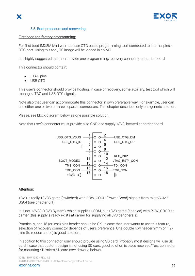
5.5. Boot procedure and recovering
First boot and factory programming: For first boot IMX8M Mini we must use OTG based programming tool, connected to internal pins - OTG port. Using this tool, OS image will be loaded in eMMC. It is highly suggested that user provide one programming/recovery connector at carrier board. This connector should contain:
• JTAG pins • USB OTG
This user’s connector should provide hosting, in case of recovery, some auxiliary, test tool which will manage JTAG and USB OTG signals. Note also that user can accommodate this connector in own preferable way. For example, user can use either one or two or three separate connectors. This chapter describes only one generic solution. Please, see block diagram below as one possible solution. Note that user’s connector must provide also GND and supply +3V3, located at carrier board.
Attention: +3V3 is really +3V3S gated (switched) with POW_GOOD (Power Good) signals from microSOM™ US04 (see chapter 6.1) It is not +3V3S (+3V3 System), which supplies uSOM, but +3V3 gated (enabled) with POW_GOOD at carrier (this supply already exists at carrier for supplying all 3V3 peripherals). Practically, one 18 (or less) pins header should be OK. In case that user wants to use this feature, selection of recovery connector depends of user’s preference. One double row header 2mm or 1.27 mm (to reduce space) is good solution. In addition to this connector, user should provide using SD card. Probably most designs will use SD card. I case that custom design is not using SD card, good solution is place reserved/Test connector for mounting SD/micro SD card (see drawing below).

ID No. THW1032 - REV. 1.2
©2018 EXOR Embedded S.r.l. - Subject to change without notice
exorint.com 37
The same discussion is valid for +3V3 (+3V3 must be gated with POW_GOOD).
Drawing below shows suggested solution for both test/reserved connectors.
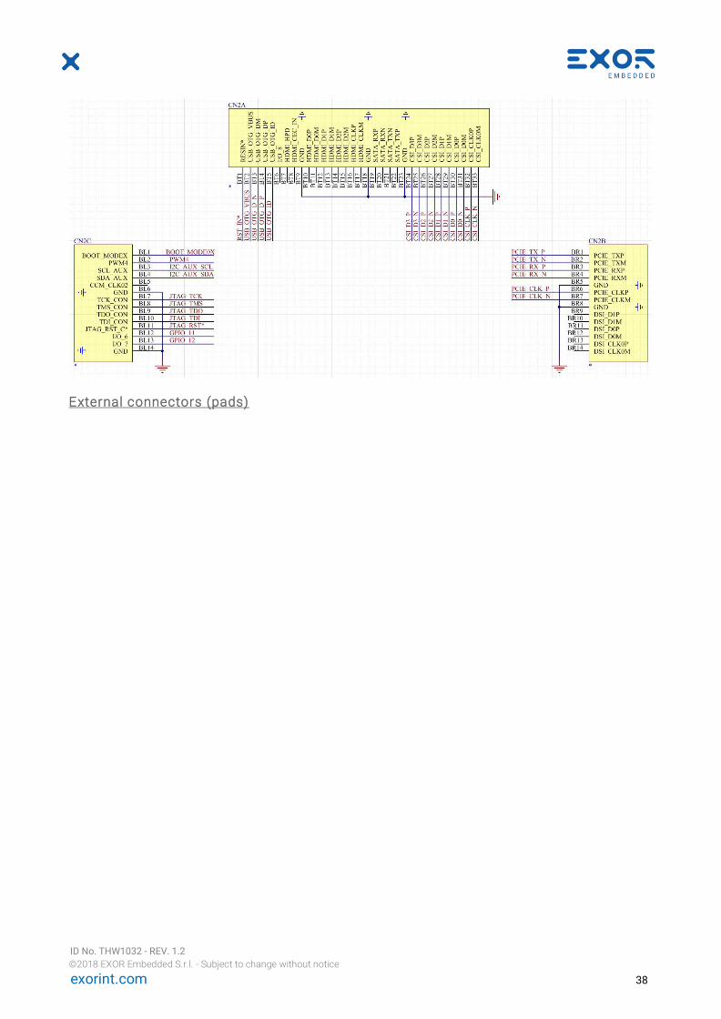
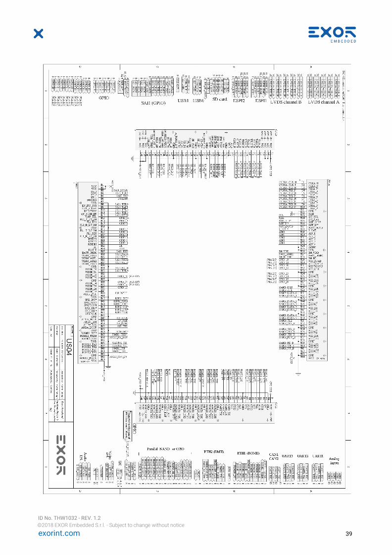
5.5. Internal and External Pads (“Connectors”)
Next two drawings show “connectors” for:
• Internal connectors (pads)
• External connectors (pads) These drawings port the same info as tables, presented before in previous chapters, and goal of these drawings is only to give customer one compact view and positions of all signals, available at pads. Internal connectors (pads)
1 33
17 18
2
Recovery /
Programming
reserved
connector
SD/uSD
card
1
12
2
11
I/O pads
I/O pads
I/O
pa
ds
I/O
pa
ds
microSOM™ US04 (mounted at carrier board)
1
1 1
1
1 1
14 14
1
ID No. THW1032 - REV. 1.2
©2018 EXOR Embedded S.r.l. - Subject to change without notice
exorint.com 38
External connectors (pads)
ID No. THW1032 - REV. 1.2
©2018 EXOR Embedded S.r.l. - Subject to change without notice
exorint.com 39
ID No. THW1032 - REV. 1.2
©2018 EXOR Embedded S.r.l. - Subject to change without notice
exorint.com 40
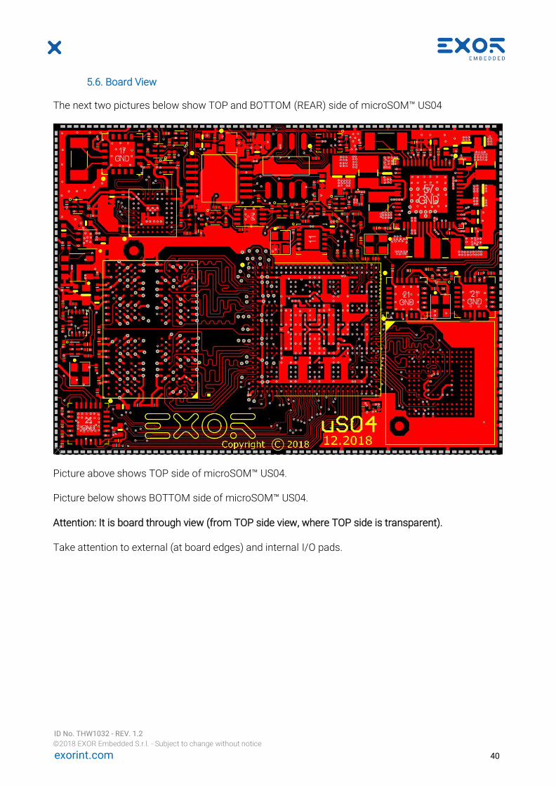
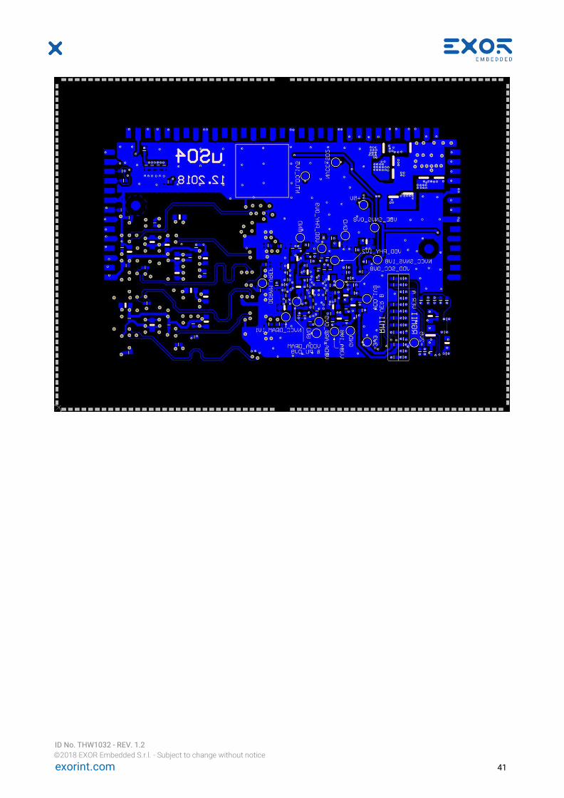
5.6. Board View
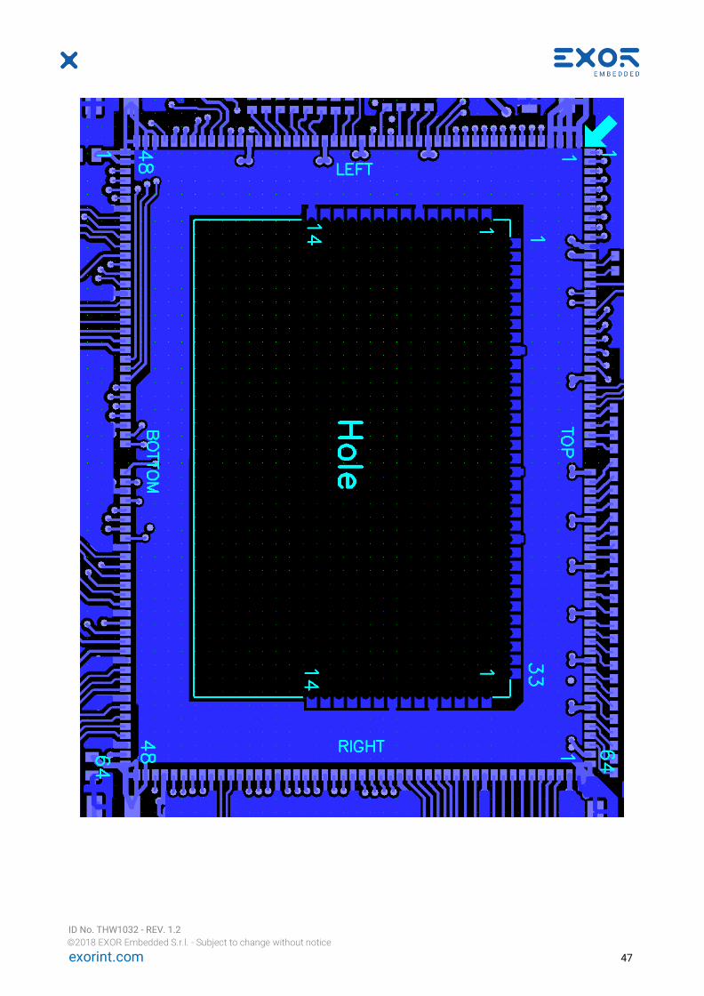
The next two pictures below show TOP and BOTTOM (REAR) side of microSOM™ US04
Picture above shows TOP side of microSOM™ US04.
Picture below shows BOTTOM side of microSOM™ US04. Attention: It is board through view (from TOP side view, where TOP side is transparent). Take attention to external (at board edges) and internal I/O pads.
ID No. THW1032 - REV. 1.2
©2018 EXOR Embedded S.r.l. - Subject to change without notice
exorint.com 41
ID No. THW1032 - REV. 1.2
©2018 EXOR Embedded S.r.l. - Subject to change without notice
exorint.com 42
6. Building carrier board shape for hosting microSOM™ US04
This chapter shows building microSOM™ US04 footprint (shape) at carrier board, where microSOM™ will be soldered. Building shape is fairly simple because pin positions are full symmetric respecting board edges (IO PADS) and virtual board center. Shortly, user must:
• Create shape outline for virtual uSOM (47.5mm x 34.9 mm) and board hole inside (35.5mm x 23.5mm).
• Create External IO PADS at board edges (48 + 64 + 48 +64).
• Create Internal IO PADS at hole edges (14 + 33 +14) We strongly suggest following this procedure in order to build appropriate carrier shape for microSOM™ US04 shape:
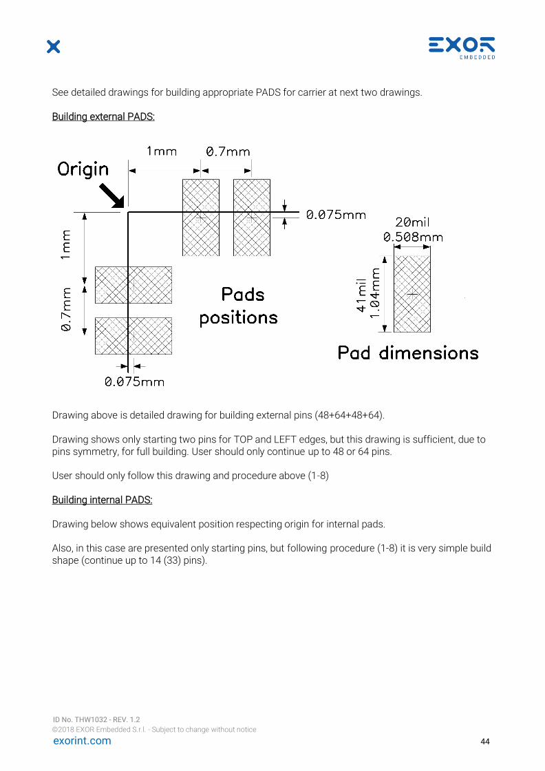
1) Outline: Draw (outline) rectangle 47.50 mm x 34.90 mm (dimensions of microSOM™)
2) Left and Right ext. connector: Place 48 rectangle PADS 1.04mm x 0.508mm (41mil x 20 mil) for external pins Left and Right sides (first PAD center is 1mm from Top edge and 0.075 mm from Left/Right edge).
3) Top and Bottom ext. connector: Place 2 x 32 (total 64 in one row) rectangle 0.508mm x
1.04mm (20mil x 41 mil) PADS for external pins Top and Bottom sides (first PAD center is 1mm from Left/Right side and 0.075mm from Top/Bottom edge). Note that between pins 32 and 33 is empty space 2.1mm (center to center).
4) Top int. connector: Place for internal conn. 33 PADS rectangle 0.7 mm x 1mm (27.5 mil x
39.3 mil). Center pin to pin distance is 1 mm. First pin center is: 7.75 mm from left edge and 5.60mm from TOP edge
5) Left and Right int. connector: Place for internal conn. twice 14 PADS for Left and Right sides
rectangle 1 mm x 0.7mm (39.3 mil x 27.5 mil). Center pin to pin distance is 1 mm. First pin center is 5.50 mm from Left/Right edge and 7.85mm from TOP edge
6) PCB hole: Provide PCB hole 35.50mm X 23.50mm. Note that PCB hole is not symmetric in Y
axis, respecting virtual board center. TOP side of carrier (under microSOM™) can be used for routing.
7) Provide some arrow at silk screen near LEFT TOP angle for board orientation (origin).
8) Provide also 4 holes (non-metallized) R=1.5mm. Holes are used for optional heat sink
mounting (for some models - TBD). Holes are symmetric and check right position in drawing below. For external IO pads (board edges):
Solder mask shape is 4 mils bigger of PAD (all edges) Solder past shape is the same as PAD

ID No. THW1032 - REV. 1.2
©2018 EXOR Embedded S.r.l. - Subject to change without notice
exorint.com 43
For internal IO pads (hole edges): Solder mask shape is 5 mils bigger of PAD (all edges) Solder past shape is the same as PAD
ID No. THW1032 - REV. 1.2
©2018 EXOR Embedded S.r.l. - Subject to change without notice
exorint.com 44
See detailed drawings for building appropriate PADS for carrier at next two drawings. Building external PADS:
Drawing above is detailed drawing for building external pins (48+64+48+64). Drawing shows only starting two pins for TOP and LEFT edges, but this drawing is sufficient, due to pins symmetry, for full building. User should only continue up to 48 or 64 pins. User should only follow this drawing and procedure above (1-8) Building internal PADS: Drawing below shows equivalent position respecting origin for internal pads. Also, in this case are presented only starting pins, but following procedure (1-8) it is very simple build shape (continue up to 14 (33) pins).

ID No. THW1032 - REV. 1.2
©2018 EXOR Embedded S.r.l. - Subject to change without notice
exorint.com 45
Some precaution: Procedure, explained above, is sufficient for carrier board shape building. All pads are built only at TOP side of carrier board. Important: This chapter highly suggests partial modification of above described internal pins (14 + 33 +14) in order to have better PADS flexibility. This procedure of internal pins building provides optionally manually re-soldering. Practically, it is suggested to build not simple only TOP side rectangle pins internal pins, (presented above), but as complex type (at the same way, as edge pins built at microSOM™)

ID No. THW1032 - REV. 1.2
©2018 EXOR Embedded S.r.l. - Subject to change without notice
exorint.com 46
Internal pads can be also smaller, but it is very important that “ARC” side of PADS is metalized. This way, we have:
1) Pads connection to all layers without classic hole. 2) Possibility of (optionally) manual re-soldering if there is need.
This chapter describes procedure for building this complex PAD in PCAD6 tool. (PCAD6 doesn’t allow directly built this type of PAD). Some newest tools probably provide this way of PADS building.
1) Create normal “through hole” PADS (explained above) with rectangle 0.7mm x 1mm at all layers for 33 pin horizontal connector and 1mm x 0.7 mm for two vertical 14 pins internal connectors.
2) Create these PADS with “virtual” hole 1mils in PAD center.
3) In production file (GBR) inform PCB manufacturer to change “virtual” hole 4) 1mm with real hole D=27mils and to move them 25mm toward board center.
5) After metallization process and removing central rectangle hole from board, we will have
these complex PADS, where part of ARC (see drawing below) will be metallized.
Picture below shows one typical carrier board for microSOM™ USO4.
30 mils
distance
from center PAD
to center HOLE30
mils
EGDE
of board
This part (ARC)
Must be
metalized
Hole
D=37mils
PAD
ID No. THW1032 - REV. 1.2
©2018 EXOR Embedded S.r.l. - Subject to change without notice
exorint.com 47
ID No. THW1032 - REV. 1.2
©2018 EXOR Embedded S.r.l. - Subject to change without notice
exorint.com 48
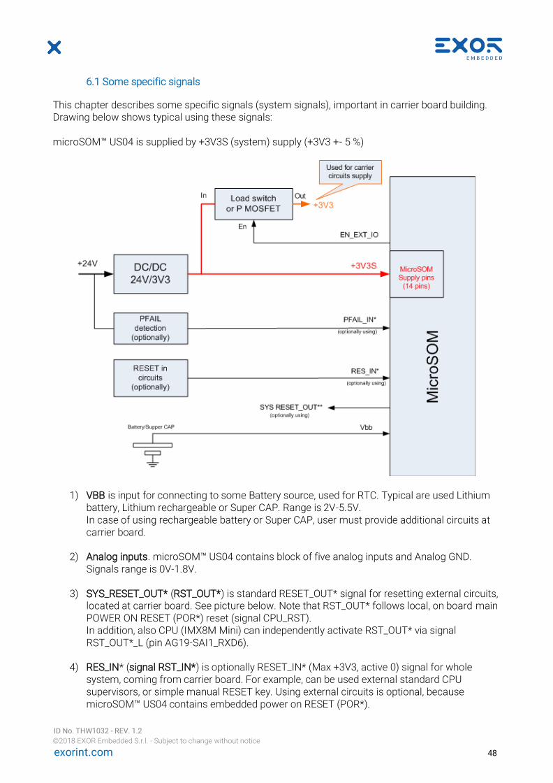
6.1 Some specific signals
This chapter describes some specific signals (system signals), important in carrier board building. Drawing below shows typical using these signals: microSOM™ US04 is supplied by +3V3S (system) supply (+3V3 +- 5 %)
1) VBB is input for connecting to some Battery source, used for RTC. Typical are used Lithium battery, Lithium rechargeable or Super CAP. Range is 2V-5.5V. In case of using rechargeable battery or Super CAP, user must provide additional circuits at carrier board.
2) Analog inputs. microSOM™ US04 contains block of five analog inputs and Analog GND.
Signals range is 0V-1.8V.
3) SYS_RESET_OUT* (RST_OUT*) is standard RESET_OUT* signal for resetting external circuits, located at carrier board. See picture below. Note that RST_OUT* follows local, on board main POWER ON RESET (POR*) reset (signal CPU_RST). In addition, also CPU (IMX8M Mini) can independently activate RST_OUT* via signal RST_OUT*_L (pin AG19-SAI1_RXD6).
4) RES_IN* (signal RST_IN*) is optionally RESET_IN* (Max +3V3, active 0) signal for whole
system, coming from carrier board. For example, can be used external standard CPU supervisors, or simple manual RESET key. Using external circuits is optional, because microSOM™ US04 contains embedded power on RESET (POR*).
ID No. THW1032 - REV. 1.2
©2018 EXOR Embedded S.r.l. - Subject to change without notice
exorint.com 49
5) PFAIL_IN* is optionally PFAIL_INTERRUPT*, for interrupting CPU in case of early power supply power detection. It could be important for backup critic application where early power down event can be used for file or application closing. In microSOM™ US04 is used GPIO1-IO05 (Pin AF12) for this purpose. It is one NMI. Typical using is connecting this signal to some comparator which controls main power supply.
6) POW_GOOD (EN_EXT_IO) is one mandatory signal (out from microSOM™ US04, active high)
to enable supply auxiliary circuits at carrier board. microSOM™ US04 is supplied by +3V3S (system) from carrier board but supply for circuits at carrier must be controlled by this signal to respect power up procedure for CPU at microSOM™.
External circuits connected to I/O pins of microSOM™ US04 shouldn’t be supplied before POW_GOOD is asserted (see drawing above).
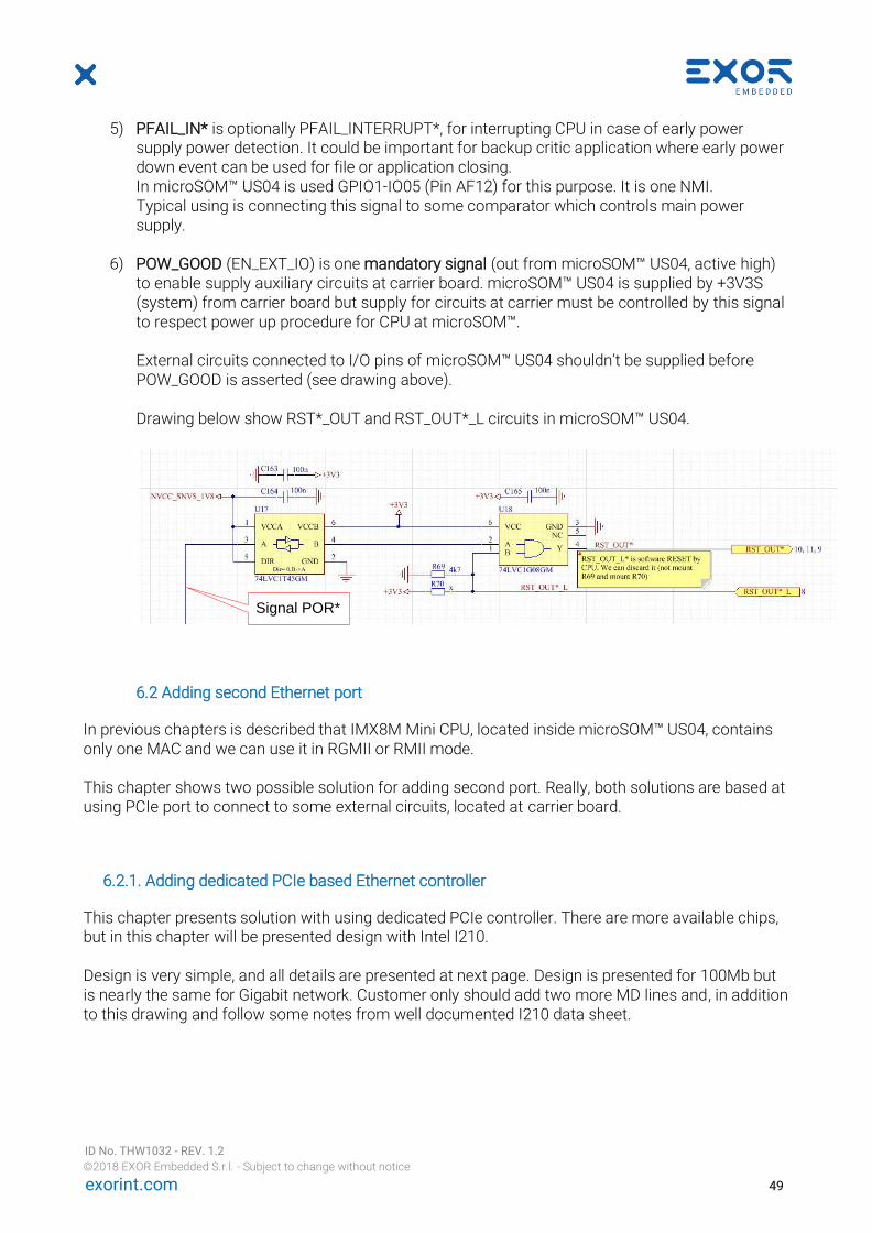
Drawing below show RST*_OUT and RST_OUT*_L circuits in microSOM™ US04.
6.2 Adding second Ethernet port
In previous chapters is described that IMX8M Mini CPU, located inside microSOM™ US04, contains only one MAC and we can use it in RGMII or RMII mode. This chapter shows two possible solution for adding second port. Really, both solutions are based at using PCIe port to connect to some external circuits, located at carrier board.
6.2.1. Adding dedicated PCIe based Ethernet controller
This chapter presents solution with using dedicated PCIe controller. There are more available chips, but in this chapter will be presented design with Intel I210. Design is very simple, and all details are presented at next page. Design is presented for 100Mb but is nearly the same for Gigabit network. Customer only should add two more MD lines and, in addition to this drawing and follow some notes from well documented I210 data sheet.
Signal POR*

ID No. THW1032 - REV. 1.2
©2018 EXOR Embedded S.r.l. - Subject to change without notice
exorint.com 50
All signals for connecting to microSOM™ US04 are coming to/from BOTTOM side. These signals are:
• PCIe_TX Pair
• PCIe_RX Pair • PCIe_CLK Pair
• PCIe_RST* Customer should take special attention to routing high speed PCIe signals (PCIe 1). It is well documented to various document which is simple find.

ID No. THW1032 - REV. 1.2
©2018 EXOR Embedded S.r.l. - Subject to change without notice
exorint.com 51
ID No. THW1032 - REV. 1.2
©2018 EXOR Embedded S.r.l. - Subject to change without notice
exorint.com 52
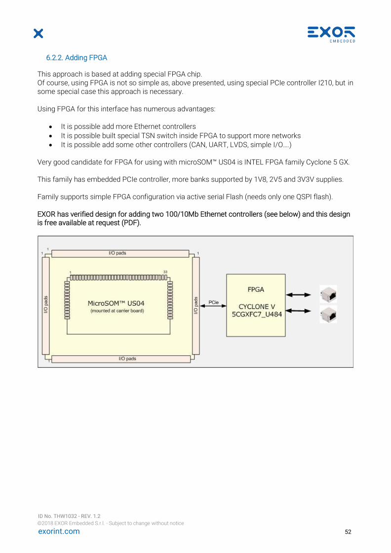
6.2.2. Adding FPGA
This approach is based at adding special FPGA chip. Of course, using FPGA is not so simple as, above presented, using special PCIe controller I210, but in some special case this approach is necessary. Using FPGA for this interface has numerous advantages:
• It is possible add more Ethernet controllers
• It is possible built special TSN switch inside FPGA to support more networks • It is possible add some other controllers (CAN, UART, LVDS, simple I/O….)
Very good candidate for FPGA for using with microSOM™ US04 is INTEL FPGA family Cyclone 5 GX. This family has embedded PCIe controller, more banks supported by 1V8, 2V5 and 3V3V supplies. Family supports simple FPGA configuration via active serial Flash (needs only one QSPI flash). EXOR has verified design for adding two 100/10Mb Ethernet controllers (see below) and this design is free available at request (PDF).


