Microstructure characterization by angle-resolvedscatter and comparison to measurements made byother techniques
R. D. Jacobson, S.and Lars Mattsson
R. Wilson, G. A. Al-Jumaily, J. R. McNeil, Jean M. Bennett,
The theory and measurement of angle-resolved scatter are described. Values of rms roughness that wereobtained by using this technique to characterize four different materials are compared with values thatwere obtained by using a total integrated scatter measuring instrument, an optical profiler, and amechanical profiler. The spatial frequency bandwidths and modulation transfer functions of the fourinstruments are different, and results are described in light of these differences.
In many areas of technology it is becoming increas-ingly important to characterize the microstructure ofsmooth surfaces. In the optics industry, which haslong been concerned with optical scatter and therelated microstructure of components, the require-ments for better, lower-scatter materials and compo-nents are becoming more demanding as optical sys-tems evolve. For example, high-energy laser opticsand laser gyro mirrors require state-of-the-art compo-nents with extremely low scatter from surfaces of< 2-A rms roughness.
Angle-resolved scatter (ARS) characterization is apromising surface diagnostic technique that is rapidand noncontact. A sample requires no special prepara-
At the time this work was performed by R. D. Jacobson, S. R.Wilson, G. A. A-Jumaily, and J. R. McNeil were with the Depart-ment of Electrical and Computer Engineering, Center for HighTechnology Materials, University of New Mexico, Albuquerque,New Mexico 87131. R. D. Jacobson is now with Sandia Systems,13423 Desert Hills, N.E., Albuquerque, New Mexico 87111. G. A.Al-Jumaily is now with the Jet Propulsion Laboratory, CaliforniaInstitute of Technology, 4800 Oak Grove Drive, Pasadena, Califor-nia 91109-8099. J. M. Bennett is with the Physics Division,Research Department, U.S. Naval Weapons Center, China Lake,California 93555. L. Mattsson is with the Institute for OpticalResearch, Royal Institute of Technology, S-10044 Stockholm,Sweden.
tion (e.g., etching or overcoating with a conductingfilm) and therefore is not destroyed as it is when someother techniques such as scanning electron micros-copy and transmission electron microscopy are used.For reflecting samples, the technique provides quanti-tative information about surface microstructure (e.g.,rms roughness, rms slope, and power spectral den-sity). For samples that transmit at the measurementwavelength, the technique can provide qualitativeinformation about the surface and also can give anindication of the microstructure in the volume of thesample. The technique has been used extensively toexamine reflecting optical samples.' 5 Similarly it hasbeen used more recently to examine silicon andgallium arsenide wafers for subsurface damage causedby polishing.6 7
Various types of instrument have been used tocharacterize smooth surfaces. 1'16 Instruments thatmeasure ARS'4 and total integrated scatter (TIS)8 9
provide information about surface microstructure.Other instruments such as mechanical profilers'>'2and optical profilers1116 measure the surface profiledirectly. The mechanical profiler is a contact devicethat can sometimes deform a surface if the material issoft or if the stylus loading is too large. It is limited toexamination of the top surface of a sample and isrelatively slow to set up for examining smooth sur-faces. In addition, the stylus response can be nonlin-ear.'7 Optical profilers are noncontacting and hencedo not damage the surface. They provide a profile orarea map of the surface. The high-frequency responseof one type of optical profiler has been shown to be
nonlinear and a method for correcting this responsehas been given.'8 If the sample under examination istransparent at the wavelength that is used, theoptical surface might be different from that examinedby the mechanical profiler. Examples include coatedsurfaces, such as laser mirrors. Although the opticaland mechanical profilers have comparable heightsensitivities, the lateral resolution of optical profilersis limited by the resolution of the optical system andcan be 20 times less than that of a mechanical profilerequipped with a submicrometer radius stylus.
The intent of this paper is to compare the ARStechnique with other techniques that are used forsurface characterization and to present data taken onthe same samples by means of the different tech-niques. The other techniques that are used for com-parison are TIS,9 profiling with a TOPO-2D opticalprofiler,'3 and a Talystep mechanical profiler. 0 TheARS measurements were performed at the Univer-sity of New Mexico, the TIS and Talystep measure-ments were performed at the Institute for OpticalResearch in Sweden, and the TOPO-2D measure-ments were performed at the Wyko Corporation inTucson, Arizona.
In the following sections we first briefly review therelation between surface microstructure and light-scatter characteristics of a sample as well as theconcepts of surface spatial wavelengths and band-width limitations of measurement techniques. TheARS apparatus is then described. Finally, other tech-niques are briefly described, and results from measure-ments made on the same samples by using thedifferent techniques are compared.
Relation between Scattered Light and Surface
Microstructure
The relation between scattering of electromagneticradiation and surface topography has been studiedfor many years, originally in the radar field.9 2 Ingeneral the connection is complicated and dependscritically on the actual surface topography. However,for a perfectly reflecting surface, and in the smooth-surface limit when the heights of the surface irregu-larities are much smaller than the wavelength of thescattered light, the relation becomes simple. Twoinvestigators who pioneered the application of vectordiffraction theories to optical scatter are Church etal.2'2 2'2 3 and Elson and Bennett.24 25 Here we followChurch's treatment in relating scattered light to thesurface roughness.
Vector scattering theories describe the differentiallight scatter d10 as23
1 d CIo = A4 Q(O,, ko, o 1 4 8, n, Xo, X,)W(p, q),Io,d XI
(1)
where C is a constant, I( is the intensity of theincident light, and dw., is the solid angle of thedetection system. The scattered intensity is propor-tional to X` as in Rayleigh and Mie scattering. Thequantity Q in Eq. (1), called the optical factor, isindependent of the surface condition and is a function
of the polar and azimuthal angles of incidence 00 and'k, scatter angles 0, and k, complex index of refrac-tion A of the surface, and polarization states of theincident and scattered light X0 and X, respectively.The surface factor W(p, q) is the power spectraldensity (PSD) of the surface roughness. The PSD canbe defined as the roughness power per unit surfacespatial frequency. Figure 1 illustrates the scattergeometry with the angles that are used in Eq. (1).
If the surface (i.e., the best-fit plane) is in the x-yplane, and Z(x, y) is the surface height variation(surface roughness) relative to that plane, the PSD isgiven by 23
W(p, q) A -ffdxdy exp[i(px + qy)]Z(x,y)}, (2)
where A is the area of the scatterer and p and q arethe surface spatial frequencies in the x and y direc-tions. In other words, Wis the average square magni-tude of the two-dimensional Fourier transform of thesurface roughness. The relation between the inten-sity of light that is scattered into a solid angle dw, andthe PSD of the surface roughness is then expressedas 2 3
I d dwe = 4k4 cos O0 cos2 0,Q'W(p, q)d(o,,I, do, (3)
where k = 27r/X is the wave number, and Q', which issometimes called the polarization factor, is nearly thesame as Q in Eq. (1) except that the functionaldependences for the incident and scatter angles aregiven explicitly. From Eq. (3) it is clear that ameasurement of the scattered light intensity as afunction of the scatter angle enables the PSD of thesurface microstructure to be calculated. The preced-ing discussion is applicable to a surface with isotropicmicrostructure as normally found in the case ofpolished surfaces. Expressions similar to Eqs. (1)-(3)can be obtained for a sample with unidirectionalstructure, such as a machined surface.
Z
Yx I
I INCIDENT BEAM
SCATTERED BEAM f
I -.-i - OPTICAL SURFACE
Fig. 1. Schematic diagram showing the notation for the ARSarrangement. Light is incident at a polar angle 0, with azimuthalangle 1, = 0; the polar and azimuthal scatter angles are O and ,,respectively.
Although the PSD contains information about thesurface roughness, it is often convenient to describethe surface roughness in terms of specific surface-finish parameters in order to better compare ARSmeasurements with those that are made by usingother types of instrument. The most commonly usedsurface-finish parameter is the rms roughness a. Asshown below, a depends on the range of surfacespatial frequenciesf, which is included in the measure-ment and is thus said to be band limited.223 Alterna-tively, the surface spatial wavelength d = 1/ f can beused to describe lateral surface structure.
The TIS from a surface is the integral of the ARSthat is obtained by using a reflecting hemisphere oran integrating sphere and is expressed in terms ofsurface roughness as2
where Rd is the diffuse reflectance, R is the totalreflectance, R is the specular reflectance, and is theilluminating wavelength. In Eq. (4) it is assumed thatthe surface is an opaque reflector, that the smooth-surface limit is valid (i.e., or << ), and that the light isnormally incident on the surface. This relation doesnot require a specific statistical distribution of sur-face heights.27 It can be obtained by integrating theARS expression in Eq. (1)27 and is valid for all anglesin the smooth surface limit.
To obtain an intuitive understanding for the rela-tion between the angular distribution of scatteredlight and the microstructure, it is useful to model thesurface roughness as a superposition of many peri-odic components. For simplicity consider a one-dimensional surface. This can be thought of as beingcomposed of components with sinusoidal height vari-ations, each with different amplitude a, spatial fre-quency f, and phase. The situation is analogous todecomposing an electrical signal into a number ofsignals that sinusoidally vary with time, as in aFourier analysis. Consider a shallow, one-dimen-sional sinusoidal amplitude variation on an otherwiseperfectly flat surface. The surface variation is givenby Z(x) = a sin(27rx/d). To satisfy the smooth-surfacelimit, the amplitude a should be sufficiently small sothat (ka)2 << 1. A beam of light incident on thissurface is diffracted into different orders on eitherside of the specular beam. In the smooth-surface limitonly first-order diffracted beams need to be consid-ered; this intensity is given by22
I (ka cos O,)2 (5)
in the limiting case when d/X >> 1. For smaller valuesof d/X, the intensity depends on the polarization stateof the incident light beam.22 The angle between thediffracted beams and the specular beam can be found
from the grating equation, which is written in thefollowing form:
Xsin 0 = sin 0 + -6
Thus light that is scattered at a specific angle Q isproduced by the surface structure of spatial wave-length d; the intensity of scattered light is propor-tional to the square of the vertical amplitude of thesurface structure.22 This equation is valid for scatter-ing in the plane of incidence, as was measured by theARS instrument described here.
The one-dimensional example given here can beextended easily to two-dimensional surfaces withspatial frequencies p and q. When the smooth-surfacecondition is satisfied, the scattered light is a simplemapping of the PSD of the surface roughness.
The one-dimensional bandwidth limits of the spa-tial wavelengths for instruments that measure ARSor TIS are obtained from Eq. (6) and the geometry ofthe particular instruments. The short spatial wave-length limit is equivalent to the incident light wave-length when the light is incident normally on thesurface and the instrument detects light that isscattered parallel to the surface (O = 90°). The longspatial wavelength limit depends on how close to thespecular beam scattered light can be measured. In thecase of ARS instruments in which the detector isscanned through the specular beam, the long spatialwavelength limit depends on the angular divergenceof the illuminating beam and the instrumental scat-tered light near the specular and incident beamdirections. In particular, the intensity of light mea-sured at small scatter angles O must be significantlygreater than the intensity of light scattered by theARS system at comparable angles from the incidentlaser beam, measured without the sample in place.28
For example, if the minimum value of 0Q at whichmeasurements are made is 0.5°, the surface spatialwavelength of the structure that is responsible for thescatter is 72 [um for = 633 nm. For TIS instru-ments, holes in the collecting hemisphere that passthe incident and specularly reflected beams deter-mine the maximum surface spatial wavelength limitof the instrument. Note that the TIS apparatus thatwas used in this investigation employed near-normalincidence, 0.3°, and only a single hole was used. Thehole determined a half-angle of 2.3 for collectingscattered light near the incident and specular beams,which corresponds to detecting scatter from a struc-ture of 15.8-pum spatial wavelength. The hole size isespecially important when characterizing samplesthat produce large amounts of near-angle scatter.Examples include diamond-turned surfaces and met-als such as molybdenum and beryllium that havelarge amounts of grain relief on their polished sur-faces.
The output of an ARS scatterometer can be ex-pressed as the PSD of the surface that is plotted as afunction of surface spatial frequency if the surface
structure consists of only microirregularities thatremain from the polishing process. In this case theassumptions of the scalar and vector scattering theo-ries are valid since there are no large scratches, pits,or other defects to produce geometrical optics scatter-ing and no variation of the optical constants on thesurface or in the subsurface. Dust and other isolateddefects, typically with dimensions in the micrometerdiameter range produce dipole scattering that is, inprinciple, handled by Mie scattering theory. Althoughno surfaces remain dust free, attempts were made tokeep scattering from this cause to a minimum. Tosummarize, in all the samples measured in this study,the scatter originated from the surface and wasprimarily microirregularity scattering.
Because of all the above-mentioned types of scatter-ing, the output of many ARS scatterometers is simplyexpressed as the bidirectional reflection distributionfunction (BRDF).29 The BRDF of a surface is closelyrelated to the scattered intensity per unit solid anglegiven in Eq. (1) when scattering is caused by surfacemicroirregularities only; it is the same except for afactor cos O., that is added to the denominator on theright-hand side of Eq. (1). The cosine-correctedBRDF'0 has an additional factor cos O. in the numera-tor and is thus identical to Eq. (1).
The preceding discussion relates only to a samplethat is completely reflecting. If the sample transmitsany of the incident beam, the scattered light origi-nates from the volume of the material, the frontsurface, and possibly the back surface of the sample.Although ARS can provide a useful diagnostic in thiscase, interpretation of the data is not straightfor-ward. In general, a high spatial frequency structurein the interior of the material, for example, willscatter primarily at large angles. However, multiplescattering in the material might extend the range ofscatter angles for this structure into the low-angleregion.
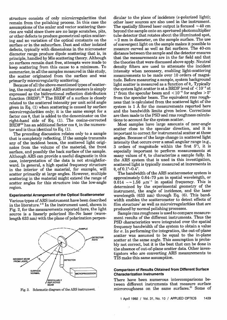
Experimental Arrangement of the Optical Scatterometer
Various types of ARS instrument have been describedin the literature. 5 In the instrument used, shown inFig. 2, for the measurements reported here, the lightsource is a linearly polarized He-Ne laser (wave-length 633 nm) with the plane of polarization perpen-
INCIDENT BEAMFROM LASER.-'
Fig. 2. Schematic diagram of the ARS instrument.
dicular to the plane of incidence (s-polarized light);other laser sources are also used in the instrument.The spatially filtered laser output is focused 40 cmbeyond the sample onto an apertured photomultipliertube detector that rotates about the illuminated spot,
2 mm in diameter, on the sample surface. The useof convergent light on the sample makes it possible tomeasure curved as well as flat surfaces. The 40-cmdistance between the sample and the detector ensuresthat the measurements are in the far field and thatthe theories that were discussed above apply. Neutraldensity filters are used to attenuate the incidentintensity when necessary, enabling light-scatteringmeasurements to be made over 10 orders of magni-tude. Before measuring a sample, system backgroundlight scatter is measured as a function of O. Typicallythe system light scatter is at a BRDF level of < 10-3 at10 from the specular beam and < 10-' for angles > 5from the specular beam. The equivalent rms rough-ness that is calculated from the scattered light of thesystem is 1 A for the measurements reported hereand the bandwidth limits given below. Correctionsare then made to the PSD and rms roughness calcula-tions to account for the system scatter.
Most samples have large amounts of near-anglescatter close to the specular direction, and it isimportant to correct for instrumental scatter at theseangles. Because of the large change in scattered lightintensity that occurs over a small angular range (e.g.,3 orders of magnitude within the first 5), it isespecially important to perform measurements atmany values of O. to characterize a sample fully. Inthe ARS system that is used in this investigation,scattered light is typically measured at increments inO of 0.1°-0.4°.
The bandwidth of the ARS scatterometer system isapproximately 0.64-70 pim in spatial wavelength, or0.014 -- 1.56 pm' in spatial frequency. This isdetermined by the experimental geometry of theinstrument, the angle of incidence, and the laserwavelength (633 nm) through Eq. (6). This band-width enables the scatterometer to detect effects offilm structure' as well as microirregularities that areproduced by normal polishing processes.
Sample rms roughness is used to compare measure-ment results of the different instruments. Thus thePSD characteristics were integrated over the spatialfrequency bandwidth of the system to obtain a valuefor a. In performing the integration, the out-of-planescatter was assumed to be equal to the in-planescatter at the same angle. This assumption is proba-bly not correct, but it is the best that can be done inthe absence of out-of-plane scatter data. Other inves-tigators who are converting ARS measurements toTIS make this same assumption.
Comparison of Results Obtained from Different SurfaceCharacterization Instruments
There have been numerous intercomparisons be-tween different instruments that measure surfacemicroroughness on the same surfaces.3' Some of
these comparisons include measurements made with4 optical profilers on 17 polished glass samples in theroughness range from < 1 to 15 A rms,32 2 opticalprofilers, a mechanical profiler, and 2 types of TISinstrument that measure a series of bare and coatedZerodur roughness standards,33 ARS and optical pro-filer measurements on polished molybdenum andaluminum-coated glass surfaces,'8 optical and mechan-ical profiler measurements on diamond-turned metalsurfaces,34 ARS and TIS measurements on diamond-turned metal samples in the roughness range 22-55A rms,35 and fringes of equal chromatic order (FECO)interferometry and TIS measurements on 12 pol-ished glass and low-scatter metal samples in theroughness range 8-27 A rms.3" In some of thesecomparisons the spatial frequency bandwidths of thedifferent instruments were not taken into account. Inother comparisons the samples contained largeamounts of near-angle scatter that were undetectedby the TIS instruments, or the samples were partiallyground and partially polished so that the lateralresolutions of the instruments were critical factors inthe measurements.
In order to have an optimum comparison for thepresent experiments, the samples chosen were allhomogeneous and opaque so that there would be noproblems with film effects, subsurface damage, oroptical constant variations. All the samples wereoptically well polished to eliminate the large amountsof near-angle scattering that are produced by mostdiamond-turned surfaces. The instrumental charac-teristics have been carefully studied. Specific descrip-tions of the instruments are given below.
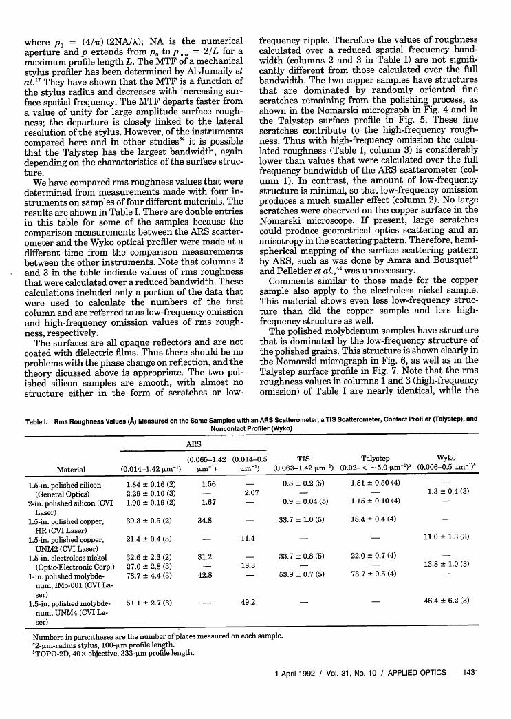
The ARS measurements were compared with mea-surements that were obtained on a TIS instrument, 9
a Wyko TOPO-2D optical profiler,'3 and a Talystepmechanical contact profiler. 0 Figure 3 illustrates thespatial wavelength bandwidths of the four instru-ments. The TIS instrument used a He-Ne laser(wavelength 633 nm) and collected light that wasscattered in the angular range from 2.30 to 820. Theinstrument sensitivity was lower at large scatterangles because of the grazing incidence angle on thedetector; an effective angular range of 2.3°-64° wasused for the intercomparison with the other instru-ments. This corresponds to a spatial wavelengthbandwidth of 0.70-15.8 pm and a spatial frequencybandwidth of 0.063-1.42 pm'. The instrument had asensitivity to detect TIS in the sub-ppm (parts in 107)range, corresponding to 0.2 A rms roughness. Aprevious intercomparison between measurements that
ARS
- nTs "~
WYKO
__- TALYSTEP
1.U 10 100
were made with a reflecting Coblentz sphere-typeinstrument and an integrating sphere-type TIS instru-ment showed excellent agreement,37 indicating thatthe effect of a variation of detector sensitivity forradiation that was scattered at large angles in theCoblentz sphere-type instrument was minimal.
The TOPO-2D optical profiler used a 40 x objective,which yielded a profile length of 333 pm. The instru-ment could measure a surface roughness of < 1 A rmsafter correcting for the 6-8 A rms roughness of theinternal reference surface.38 The pixel size and diffrac-tion limit in the microscope objective yielded a theoret-ical lateral resolution of 0.67 pm. However otherinstrument errors increased the actual lateral resolu-tion to larger values; a lateral resolution of 2 pmwas previously measured on one such instrument.39
Thus a realistic surface spatial wavelength band-width for the TOPO-2D instrument with a 40xobjective is 2-166 pm, which corresponds to a spatialfrequency bandwidth of 0.006-0.5 pum-'.
The Talystep surface profiling instrument used astylus of 2-pum radius, and the profile length was 100pm. This profile length was chosen because thesurface spatial wavelengths in the profile matchedthose in the scatter measurements reasonably well.Although the sampling distance was 0.03 pum, thelateral resolution of the instrument was limited bythe stylus radius to be > 0.2 pm, depending on thesurface slopes and structure on the surface.'7 Thusthe spatial wavelength bandwidth was > 0.2-50pm, which corresponds to a spatial frequency range of0.02- < 5 pLm-1.
Another factor that must be considered in compar-ing measurements that are made by different instru-ments is the modulation transfer function (MTF) ofthe instrument. The MTF is obtained either directlyor indirectly by Fourier transformation of the im-pulse response of the measurement instrument. 7 Ifresults from two instruments are to be compared,ideally the bandwidths and MTF characteristics ofthe instruments should be identical; the characteris-tics should at least be known. The rms roughness thatis measured is given in terms of the instrumentbandwidth and the MTF G(p, q) as
o.2 = fp dp fqm- dq G(p, q)W(p, q), (7)
where W(p, q) is given in Eq. (2). Different values ofo 2 will result if the integral limits (i.e., bandwidths) orthe MTF's of the instruments differ.
The MTF characteristic of the optical scatterome-ter is approximately unity when the angle of inci-dence is close to the surface normal,40 as is the MTFfor the TIS instrument if large scatter angles areavoided."35 The MTF characteristics of the opticalprofiler are not as well established.8 4' Church et al.42
have suggested that in one dimension of frequencyspace the MTF of this instrument has the form
Fig. 3. Illustration of the spatial wavelength bandwidths for fourinstruments. (8)
IU.1
where p0 = (4/r) (2NA/X); NA is the numericalaperture and p extends from p0 toPm,. = 2/L for amaximum profile length L. The MTF of a mechanicalstylus profiler has been determined by Al-Jumaily etal.'7 They have shown that the MTF is a function ofthe stylus radius and decreases with increasing sur-face spatial frequency. The MTF departs faster froma value of unity for large amplitude surface rough-ness; the departure is closely linked to the lateralresolution of the stylus. However, of the instrumentscompared here and in other studies34 it is possiblethat the Talystep has the largest bandwidth, againdepending on the characteristics of the surface struc-ture.
We have compared rms roughness values that weredetermined from measurements made with four in-struments on samples of four different materials. Theresults are shown in Table I. There are double entriesin this table for some of the samples because thecomparison measurements between the ARS scatter-ometer and the Wyko optical profiler were made at adifferent time from the comparison measurementsbetween the other instruments. Note that columns 2and 3 in the table indicate values of rms roughnessthat were calculated over a reduced bandwidth. Thesecalculations included only a portion of the data thatwere used to calculate the numbers of the firstcolumn and are referred to as low-frequency omissionand high-frequency omission values of rms rough-ness, respectively.
The surfaces are all opaque reflectors and are notcoated with dielectric films. Thus there should be noproblems with the phase change on reflection, and thetheory dicussed above is appropriate. The two pol-ished silicon samples are smooth, with almost nostructure either in the form of scratches or low-
frequency ripple. Therefore the values of roughnesscalculated over a reduced spatial frequency band-width (columns 2 and 3 in Table I) are not signifi-cantly different from those calculated over the fullbandwidth. The two copper samples have structuresthat are dominated by randomly oriented finescratches remaining from the polishing process, asshown in the Nomarski micrograph in Fig. 4 and inthe Talystep surface profile in Fig. 5. These finescratches contribute to the high-frequency rough-ness. Thus with high-frequency omission the calcu-lated roughness (Table I, column 3) is considerablylower than values that were calculated over the fullfrequency bandwidth of the ARS scatterometer (col-umn 1). In contrast, the amount of low-frequencystructure is minimal, so that low-frequency omissionproduces a much smaller effect (column 2). No largescratches were observed on the copper surface in theNomarski microscope. If present, large scratchescould produce geometrical optics scattering and ananisotropy in the scattering pattern. Therefore, hemi-spherical mapping of the surface scattering patternby ARS, such as was done by Amra and Bousquet4 3
and Pelletier et al.,44 was unnecessary.Comments similar to those made for the copper
sample also apply to the electroless nickel sample.This material shows even less low-frequency struc-ture than did the copper sample and less high-frequency structure as well.
The polished molybdenum samples have structurethat is dominated by the low-frequency structure ofthe polished grains. This structure is shown clearly inthe Nomarski micrograph in Fig. 6, as well as in theTalystep surface profile in Fig. 7. Note that the rmsroughness values in columns 1 and 3 (high-frequencyomission) of Table I are nearly identical, while the
Table . Rms Roughness Values (A) Measured on the Same Samples with an ARS Scatterometer, a TIS Scatterometer, Contact Profiler (Talystep), andNoncontact Profiler (Wyko)
Numbers in parentheses are the number of places measured on each sample.'2-pum-radius stylus, 100-pm profile length.'TOPO-2D, 40x objective, 333-pm profile length.
tt tu s i 00 ti i tFig. 4. Nomarski micrograph of the surface of a polished copper
sample.
roughness in column 2 (low-frequency omission) isabout half that of column 1. The distinct grainstructure of the molybdenum sample is still in theregime of the microirregularity scalar and vectorscattering theories, and the surface is isotropic whenilluminated by laser beams that are 1-2 mm indiameter, No large scratches were seen on the surfacein the Nomarski microscope.
To show the different distributions of structure onthe copper and molybdenum samples, the PSD char-acteristics for these two materials are plotted on thegraph in Fig. 8. Note that the low-frequency end ofthe PSD curve for the molybdenum sample is consid-erably above that for the copper sample, while thehigh-frequency end of the curve for copper is abovethat for molybdenum. It should be clear from thisfigure why the low-frequency omission in the case ofmolybdenum changes the roughness so much, whilethe high-frequency omission has relatively little ef-fect. The reverse is true for copper.
In comparing measurements of the ARS scatterom-eter with those of the TIS instrument, we note thatthe TIS instrument does not have a low-spatialfrequency detection limit that is equivalent to that ofthe AIRS scatterometer. Because of the hole in theCoblentz hemisphere, scattered light that is closerthan 2.3° to the specular direction is not collected.
SCAN LENGTH (pm)
Fig. 5. Talystep surface profile of a polished copper sample.
I . I1 00 gum
Fig. 6. Nomarski micrograph of the surface of a polished molybde-num sample.
The low-frequency omission for the ARS calculationsproduces the values in column 2 of Table I, therebybringing the bandwidths of the two instruments intobetter agreement. By comparing columns 2 and 4, onecan see that the values of rms roughness determinedby the two instruments agree well for polished cop-per; values in column four are slightly lower for thetwo polished silicon samples and slightly higher forthe polished electroless nickel sample. The smalldifference for the two silicon samples may be causedby the difference in spot size of the two instruments,as discussed below, or possibly by the instrumentalnoise level. The only large discrepancy in roughnessvalues is for the molybdenum sample. Recall thatboth instruments use a He-Ne laser output at 633nm. The illuminating spot is 2 mm in diameter onthe surface for the ARS scatterometer and 1 mm indiameter for the TIS instrument; any defects on thesurface that lie within the illuminated area willproduce increased light scatter. The ARS measure-ments are averages of two typical places on eachsurface. However, 29 different spots were sampled forthe TIS measurements, and the values quoted in thetable are averages of the 5 spots with the lowestscatter values. The differences between the values forthe molybdenum sample may be caused by differentspots illuminated on the sample; in retrospect, it
Fig. 8. Curves of the PSD for molybdenum and copper obtainedfrom ARS scatterometer measurements.
would have been better to make ARS measurementsat more places on the surface to obtain better statis-tics. Alternatively, the different values may representdifferences between the two instruments. The TISinstrument is less sensitive to light striking thedetector at large angles of incidence, so the highspatial frequencies (short spatial wavelengths) areweighted somewhat less than the lower spatial fre-quencies. In the ARS instrument, the detector isalways normal to the scattered light, but the beamfocus at the detector degrades at large scatteringangles. 4 0
The Wyko optical profiler cannot detect a samplestructure of spatial frequency 0.5 pm-' and higher.Therefore the scatterometer values of rms roughnesswere calculated over the bandwidth of 0.5 pm andlower in column 3 of Table I (high-frequency omis-sion) to match the high-frequency cutoff of the Wykoinstrument. There is good agreement between theroughness values that were measured for the copperand molybdenum samples (columns 3 and 6). TheWyko measurements of roughness yielded values thatare smaller for the silicon and electroless nickelsamples. The differences may be caused by differentlocations on the samples. In this comparison, measure-ments were made at three different places on eachsample with each instrument.
The Talystep roughness values given in column 5 ofTable I should best match the ARS scatterometerroughness values in column 1. There is good agree-ment for the measurements of the two silicon samplesand the molybdenum sample and poor agreement forthe polished copper and electroless nickel samples;the ARS roughness values are larger. It appears thatthe Talystep may not be detecting the high-frequencystructure on these surfaces as well as the ARSscatterometer. This might be due to the deformationof the relatively soft surfaces by the stylus, as men-tioned above. Another possibility for this discrepancycould be due to the 2-mm-diameter spot of the ARSinstrument illuminating isolated surface defects inaddition to the microirregularities profiled by theTalystep. If isolated defects occur in a Talystepprofile, they are generally eliminated by moving to adifferent spot on the surface and taking a new profile.
The fact that the microroughness values from thefour Talystep profiles measured on each sample agreedquite well indicates that the surface microroughnessremained relatively constant over the sample.
At first glance it might appear that we are compar-ing apples and oranges by comparing measurementsmade with instruments that measure an averageeffect of illumination over an area (ARS and TISmeasurements) with those that measure profiles overa one-dimensional direction on the surface (Wyko andTalystep profilers). However, here we are not compar-ing one- and two-dimensional power spectral densityfunctions as was done previously.'8 4 We are compar-ing band-limited values of the rms surface roughness.These are measured directly with the Wyko andTalystep profilers; scalar and vector scattering theo-ries are used to calculate the roughness from TIS andARS measurements.45 The agreement for this seriesof measurements is considerably better than thatobtained in a previous comparison between ARS andTIS measurements on three diamond-turned samplesand one front surface aluminum mirror.35 The sam-l les of that previous work had a roughness of 20-55
A rms when the spatial frequency bandwidths ofthose measurements were adjusted to be the same.Thus the agreement for the present set of measure-ments is encouraging.
Conclusions
In conclusion, an optical scatterometer that measuresangle-resolved light scatter, which is capable of char-acterizing the microstructure on smooth reflectingsurfaces as well as providing quantitative informa-tion about surface and bulk scatter in transparentmaterials, has been described. Roughness measure-ments that were made with this scatterometer havebeen compared with measurements that were madeon the same samples by three other instruments.Although the bandwidths and MTF's of the fourinstruments are different, when the bandwidth of thescatterometer was effectively changed to match moreclosely the bandwidths of the other instruments,reasonable agreement has been obtained.
References and Notes1. G. A. Al-Jumaily, S. R. Wilson, J. J. McNally, J. R. McNeil,
J. M. Bennett, and H. H. Hurt, "Influence of metal films on theoptical scatter and related microstructure of coated surfaces,"Appl. Opt. 25, 3631-3634 (1986); G. A. Al-Jumaily, "Influenceof metal films on the optical scatter and related surfacemicrostructure of coated surfaces," Ph.D. dissertation (Univer-sity of New Mexico, Albuquerque, N.M., 1986).
2. E. L. Church, H. A. Jenkinson, and J. M. Zavada, "Measure-ment of the finish of diamond-turned metal surfaces bydifferential light scattering," Opt. Eng. 16, 360-374 (1977).
3. L. D. Brooks and W. L. Wolfe, "Microprocessor-based instru-mentation for bidirectional reflectance distribution function(BRDF) measurements from visible to far infrared (FIR)," inRadiation Scattering in Optical Systems I, W. H. Hunt, ed.,Proc. Soc. Photo-Opt. Instrum. Eng. 257, 177-183 (1980).
4. P. Roche and E. Pelletier, "Characterizations of optical sur-faces by measurement of scattering distribution," Appl. Opt.23, 3561-3566 (1984).
5. J. C. Stover, F. M. Cady, and E. Sklar, "Measurement of lowangle scatter," Opt. Eng. 24, 404-407 (1985).
6. R. M. Silva, F. D. Orazio, Jr., and J. M. Bennett, "Nondestruc-tive measurement of subsurface structural defects in polishedsingle-crystal silicon," Opt. News 12(2), 10-17 (1986).
7. R. M. Silva, F. D. Orazio, Jr., and J. M. Bennett, "Subsurfacestructural defects in GaAs wafers," Semicond. Int. 9(7), 81-87(1986).
8. H. E. Bennett, "Scattering characteristics of optical materials,"Opt. Eng. 17, 480-488 (1978).
9. L. Mattsson, "Total integrated scatter measurement systemfor quality assessment of coatings on optical surfaces," in ThinFilm Technologies, J. R. Jacobsson, ed., Proc. Soc. Photo-Opt.Instrum. Eng. 652, 264-271 (1986).
10. Talystep Surface Profiler sold by Rank Taylor Hobson, 411East Jarvis Avenue, Des Plaines, Ill. 60018. See also J. M.Bennett and J. H. Dancy, "Stylus profiling instrument formeasuring statistical properties of smooth optical surfaces,"Appl. Opt. 20, 1785-1802 (1981).
12. Dektak IIA and Dektak 3030 manufactured by Veeco Instru-ments, Inc., Sloan Technology Division, 602 East MontecitoStreet, Santa Barbara, Calif. 93103.
13. Wyko TOPO-2D and TOPO-3D manufactured by Wyko Corpo-ration, 2650 Elvira Road, Tucson, Ariz. 85706. See also B.Bushan, J. C. Wyant, and C. L. Koliopoulos, "Measurement ofsurface topography of magnetic tapes by Mirau inter-ferometry," Appl. Opt. 24, 1489-1497 (1985).
14. Heterodyne Profiler, Model 5500, manufactured by Zygo Cor-poration, Laurel Brook Road, P.O. Box 448, Middlefield, Conn.06455. See also G. E. Sommargren, "Optical heterodyneprofilometry," Appl. Opt. 20, 610-618 (1981).
15. Laser Interferometric Microscope, Maxim 3D, manufacturedby Zygo Corporation, address same as in Ref. 14.
16. MP 2000 Non-Contact Surface Profiler manufactured byChapman Instruments, Inc., 50 Saginaw Drive, Rochester,N.Y. 14623. See also T. C. Bristow, A. Bouzid, and J. Bietry,"Surface measurements and applications for manufacturedparts using noncontact profilometer," in Optical Testing andMetrology II, C. P. Grover, ed., Proc. Soc. Photo-Opt. Instrum.Eng. 954, 217-225 (1988).
17. G. A. Al-Jumaily, S. R. Wilson, K. C. Jungling, J. R. McNeil,and Jean M. Bennett, "Frequency response characteristics of amechanical surface profilometer," Opt. Eng. 26, 953-958(1987).
18. E. L. Church, P. Z. Takacs, and T. A. Leonard, "The predictionof BRDFs from surface profile measurements," in Scatter fromOptical Components, J. C. Stover, ed., Proc. Soc. Photo-Opt.Instrum. Eng. 1165, 136-150 (1990).
19. H. Davies, "The reflection of electromagnetic waves from arough surface," Proc. Inst. Electr. Eng. Part 4 101, 209-214(1954).
20. P. Beckmann and A. Spizzichino, The Scattering of Electromag-netic Waves from Rough Surfaces, (Pergamon, London, 1963),and references contained therein.
21. See the feature on waves in random media, J. Opt. Soc. Am. A2(12) (1985).
22. E. L. Church and J. M. Zavada, "Residual roughness ofdiamond-turned optics," Appl. Opt. 14, 1788-1795 (1975).
23. E. L. Church, H. A. Jenkinson, and J. M. Zavada, "Relation-ship between surface scattering and microtopographicfeatures," Opt. Eng. 18, 125-136 (1979).
24. J. M. Elson and J. M. Bennett, "Relation between the angulardependence of scattering and the statistical properties ofsmooth optical surfaces," J. Opt. Soc. Am. 69, 31-47 (1979).
25. J. M. Elson and J. M. Bennett, "Vector scattering theory,"Opt. Eng. 18, 116-124 (1979).
26. H. E. Bennett and J. 0. Porteus, "Relation between surfaceroughness and specular reflectance at normal incidence," J.Opt. Soc. Am. 51, 123-129 (1961).
27. J. M. Elson, J. P. Rahn, and J. M. Bennett, "Relationship ofthe total integrated scattering from multilayer-coated optics toangle of incidence, polarization, correlation length, and rough-ness cross-correlation properties," Appl. Opt. 22, 3207-3219(1983).
28. Small scatter angles strictly refer to small angles measuredrelative to the specular direction. However, in both the ARSand TIS instruments the angle of incidence was very close tonormal so that the incident and reflected angles were essen-tially 00.
29. F. E. Nicodemus, "Directional reflectance and emissivity of anopaque surface," Appl. Opt. 4, 767-771 (1965); 5, 715(E)1966);-"Reflectance nomenclature and directional reflectanceand emissivity," Appl. Opt. 9, 1474-1475 (1970).
30. J. C. Stover, "Optical scatter," Lasers Optron. 7(8), 61-69(August 1988).
31. J. M. Bennett and L. Mattsson, Introduction to SurfaceRoughness and Scattering (Optical Society of America, Wash-ington, D. C., 1989), pp. 31-37.
32. N. J. Brown and W. K. Eickelberg, "Some comparisons ofnoncontact surface profiling instruments," in Optical Fabrica-tion and Testing, Vol. 12 of OSA Technical Digest Series(Optical Society of America, Washington, D.C., 1988), pp.52-55.
33. J. M. Bennett, "Comparison of techniques for measuring theroughness of optical surfaces," Opt. Eng. 24, 380-387 (1985).
34. E. L. Church, T. V. Vorburger, and J. C. Wyant, "Directcomparison of mechanical and optical measurements of thefinish of precision machined optical surfaces," Opt. Eng. 24,388-395 (1985).
35. J. C. Stover, B. Hourmand, J. A. Kahler, and C. H. Gillespie,"Comparison of roughness measurements by differential scat-ter and total integrated scatter," in Stray Radiation IV, R. P.Breault, ed., Proc. Soc. Photo-Opt. Instrum. Eng. 511, 2-6(1984).
36. J. M. Bennett, "Measurement of the rms roughness, autoco-variance function, and other statistical properties of opticalsurfaces using a FECO scanning interferometer," Appl. Opt.15, 2705-2721 (1976).
37. K. H. Guenther, P. G. Wierer, and J. M. Bennett, "Surfaceroughness measurements of low-scatter mirrors and rough-ness standards," Appl. Opt. 23, 3820-3836 (1984).
38. K. Creath and J. C. Wyant, "Absolute measurement of surfaceroughness," Appl. Opt. 29, 3823-3827 (1990).
39. J. M. Bennett, T. C. Bristow, K. Arackellian, and J. C. Wyant,"Surface profiling with optical and mechanical instruments,"in Technical Digest on Optical Fabrication and Testing (Opti-cal Society of America, Washington, D.C., 1986), paper ThB4;see also Ref. 31, pp. 14-15.
40. J. C. Stover and B. Hourmand, "Some deviations associatedwith vector perturbation diffraction theory," in Stray Radia-tion IV, R. P. Breault, ed., Proc. Soc. Photo-Opt. Instrum. Eng.511, 12-17 (1984).
41. E. L. Church and P. Z. Takacs, "Effects of the optical transferfunction in surface profile measurements," in Surface Charac-terization and Testing II, J. E. Greivenkamp and M. Young,eds., Proc. Soc. Photo-Opt. Instrum. Eng. 1164, 46-59 (1989).
42. E. L. Church, G. M. Sanger, and P. Z. Takacs, "Comparison ofWyko and TIS measurement of surface finish," in Metrology:Figure and Finish, B. Truax, ed., Proc. Soc. Photo-Opt.Instrum. Eng. 749, 65-73 (1987).
43. C. Amra and P. Bousquet, "Scattering from surfaces andmultilayer coatings: Recent advances for a better investiga-
tion of experiment," in Surface Measurement and Character-ization, J. M. Bennett, ed., Proc. Soc. Photo-Opt. Instrum.Eng. 1009, 82-97 (1988); see also earlier papers listed in thereferences.
44. E. Pelletier, R. Roche, and C. Grezes-Besset, in SurfaceMeasurement and Characterization, J. M. Bennett, ed., Proc.Soc. Photo-Opt. Instrum. Eng. 1009, 98-110 (1988); see alsoearlier papers listed in the references.
45. A reviewer has suggested that the rms roughness measure-ments for the Wyko profiler (and presumably also for theTalystep profiler) should have been calculated from a two-dimensional PSD rather than measured directly on a one-dimensional profile. His back-of-the-envelope calculations for
the two-dimensional case assume a constant slope for the PSDwhen plotted on a log-log scale and yield roughness values thatare higher than those measured by using the Wyko instru-ment. He thus is suggesting that a two-dimensional roughnessmeasured by a profiler on an isotropic surface should be largerthan a one-dimensional roughness measured by the profiler onthe same surface. Possible differences between one- and two-dimensional roughnesses on isotropic surfaces should be care-fully checked before drawing any firm conclusions. However,
the intention of this investigation was to present results fromdifferent measurement techniques by using accepted analysismethods.


![Scatter Business Deck - [1477]](https://static.documents.pub/doc/80x56/58f04f401a28abfa368b466f/scatter-business-deck-1477.jpg)