52


Microwave Circuit Design

This page intentionally left blank

Microwave Circuit Design
A Practical Approach Using ADS
Kyung-Whan Yeom
New York • Boston • Indianapolis • San Francisco Toronto • Montreal • London • Munich • Paris • Madrid
Capetown • Sydney • Tokyo • Singapore • Mexico City

Many of the designations used by manufacturers and sellers to distinguish their products are claimed as trademarks. Where those designations appear in this book, and the publisher was aware of a trademark claim, the designations have been printed with initial capital letters or in all capitals.
The author and publisher have taken care in the preparation of this book, but make no expressed or implied warranty of any kind and assume no responsibility for errors or omissions. No liability is assumed for incidental or consequential damages in connection with or arising out of the use of the information or programs contained herein.
For information about buying this title in bulk quantities, or for special sales opportunities (which may include electronic versions; custom cover designs; and content particular to your business, training goals, marketing focus, or branding interests), please contact our corporate sales department at [email protected] or (800) 382-3419.
For government sales inquiries, please contact [email protected].
For questions about sales outside the United States, please contact [email protected].
Visit us on the Web: informit.com/ph
Library of Congress Cataloging-in-Publication DataYeom, Kyung-Whan. Microwave circuit design : a practical approach using ADS / Kyung-Whan Yeom. pages cm Includes index. ISBN 978-0-13-408678-1 (hardcover : alk. paper)—ISBN 0-13-408678-3 1. Microwave circuits—Computer-aided design. 2. Advanced design system. I. Title. TK7876.Y46 2015 621.381'32—dc23 2015004174
Copyright © 2015 Pearson Education, Inc.
ADS (Advanced Design System) is a trademark of Keysight Technologies. HFSS (High Frequency Structure Simulator) is a trademark of ANSYS, Inc. Mathcad is a trademark of PTC Inc. Keysight Technologies, Inc. makes no warranty as to the accuracy or completeness of the foregoing material and hereby disclaims any responsibility therefor. Copyright 2000–2014 Keysight Technologies, Inc. Reproduced with permission.
All rights reserved. Printed in the United States of America. This publication is protected by copyright, and permission must be obtained from the publisher prior to any prohibited reproduction, storage in a retrieval system, or transmission in any form or by any means, electronic, mechanical, photocopying, recording, or likewise. To obtain permission to use material from this work, please submit a written request to Pearson Education, Inc., Permissions Department, 200 Old Tappan Road, Old Tappan, New Jersey 07675, or you may fax your request to (201) 236-3290.
ISBN-13: 978-0-13-408678-1 ISBN-10: 0-13-408678-3 Text printed in the United States on recycled paper at Edwards Brothers Malloy in Ann Arbor, Michigan. First printing May, 2015

To my wife Cho Soon-Duk (조순덕) and son Yeom Jae-Hyung (염재형)

This page intentionally left blank

vii
Contents
Preface xiii
Acknowledgments xv
About the Author xvii
Chapter 1 Microwave Integrated Circuits 1
1.1 Classification of Microwave Integrated Circuits 11.2 Microwave Circuits in a Communication System 61.3 Summary 9
Chapter 2 Passive Devices 11
2.1 Impedances 112.2 Classification 122.3 Equivalent Circuits 16
2.3.1 Chip-Type Capacitors 162.3.2 Chip-Type Inductors 192.3.3 Chip-Type Resistors 21
2.4 Impedance Measurements 222.5 Summary 26
Chapter 3 Transmission Lines 29
3.1 Introduction 293.2 Parameters 30
3.2.1 Phase Velocity 303.2.2 Wavelength 353.2.3 Characteristic Impedance 373.2.4 Measurements 39
3.3 Coaxial and Microstrip Lines 403.3.1 Coaxial Line 403.3.2 Microstrip Line 44

viii Contents
3.4 Sinusoidal Responses 503.4.1 Phasor Analysis 503.4.2 Reflection and Return Loss 523.4.3 Voltage Standing Wave Ratio (VSWR) 54 3.4.4 Smith Chart and Polar Chart 57
3.5 Applications 603.5.1 Short-Length Transmission Line 603.5.2 Resonant Transmission Line 603.5.3 Two-Port Circuit Application 69
3.6 Discontinuities 763.6.1 Open-End Microstrip 763.6.2 Step and Corner Discontinuities 783.6.3 T-Junction and Cross Junction 79
3.7 Summary 80
Chapter 4 S-parameters and Noise Parameters 87
4.1 S-parameters 874.1.1 Voltage S-Parameter Definition 884.1.2 Definitions and Properties of S-Parameters 954.1.3 Ports and S-Parameter Simulation 974.1.4 S-Parameter Conversion 994.1.5 Shift of Reference Planes 1034.1.6 Insertion Loss and Return Loss 1084.1.7 Input Reflection Coefficient 110
4.2 Noise Parameters 1124.2.1 Expression of Internal Noise 1124.2.2 Representation of Noise Signals 1134.2.3 Noise Figure 1224.2.4 Expression of Noise Parameters 1244.2.5 Frii’s Formula 1334.2.6 Measurement of Noise Figure and Noise Parameters 136
4.3 File Formats 1404.4 Summary 142
Chapter 5 Introduction to Microwave Active Devices 149
5.1 Introduction 1495.2 Field Effect Transistor (FET) 151
5.2.1 GaAs MESFET 1525.2.2 Large-Signal Equivalent Circuit 1545.2.3 Simplified Small-Signal Equivalent Circuit and S-Parameters 157 5.2.4 Package 1595.2.5 GaAs pHEMT 161
5.3 Bipolar Junction Transistor (BJT) 162 5.3.1 Operation of an Si BJT 1625.3.2 Large-Signal Model of a BJT 165 5.3.3 Simplified Equivalent Circuit and S-Parameters 1685.3.4 Package 1715.3.5 GaAs/AlGaAs HBT 172

ixContents
5.4 DC-Bias Circuits 1735.4.1 BJT DC-Bias Circuits 1735.4.2 FET DC-Bias Circuit Design 177 5.4.3 S-Parameter Simulation 178
5.5 Extraction of Equivalent Circuits 1815.6 Summary 195
Chapter 6 Impedance Matching 201
6.1 Introduction 2016.2 Maximum Power Transfer Theorem 2026.3 Discrete Matching Circuits 205
6.3.1 Series-to-Parallel Conversion 2056.3.2 L-Type Matching Circuit 2076.3.3 A p-Type Matching Circuit 2126.3.4 T-Type Matching Circuit 2146.3.5 Double L-Type Matching Circuit 2166.3.6 Matching Circuit Design for a General Source Impedance 217
6.4 Transmission-Line Matching Circuits 2196.4.1 Single-Stub Tuner 2196.4.2 Impedance Inverter 223
6.5 Summary 224
Chapter 7 Simulation and Layout 227
7.1 Simulation in ADS 2277.2 Circuit Simulations 230
7.2.1 Classification of Circuit Simulations 2307.2.2 DC Simulation 2307.2.3 Transient Simulation 2347.2.4 AC Simulation 2377.2.5 Harmonic Balance Simulation 2397.2.6 Multi-Tone Harmonic Balance 2437.2.7 Optimization 246
7.3 Layout 2487.3.1 Layout Example 2507.3.2 Layer Preparation for Layout 250 7.3.3 Layout Units and Grid Set 2537.3.4 Outline Setting 2547.3.5 Component Layout 2567.3.6 Layout Using Components 262
7.4 Momentum 2647.4.1 Theory 264 7.4.2 Settings and EM Simulation 267
7.5 Summary 276
Chapter 8 Low-Noise Amplifiers 279
8.1 Introduction 2798.2 Gains 281
8.2.1 Definition of Input and Output Reflection Coefficients 281

x Contents
8.2.2 Thevenin Equivalent Circuit 2828.2.3 Power Gains 286
8.3 Stability and Conjugate Matching 2928.3.1 Load and Source Stability Regions 293 8.3.2 Stability Factor 2968.3.3 Conjugate Matching 301
8.4 Gain and Noise Circles 3068.4.1 Gain Circles 306 8.4.2 Noise Circles 308
8.5 Summary of Gains and Circles 3118.5.1 Summary of Gains 311 8.5.2 Summary of Circles 312
8.6 Design Example 3148.6.1 Design Goal 3148.6.2 Active Device Model 314 8.6.3 Device Performance 3158.6.4 Selection of Source and Load Impedances 3198.6.5 Matching Circuit Design 3228.6.6 DC Supply Circuit 330 8.6.7 Stability 3338.6.8 Fabrication and Measurements 336
8.7 Summary 345
Chapter 9 Power Amplifiers 351
9.1 Introduction 3519.2 Active Devices for Power Amplifiers 355
9.2.1 GaN HEMT 3569.2.2 LDMOSFET 360
9.3 Optimum Load Impedances 3619.3.1 Experimental Load-Pull Method 362 9.3.2 Load-Pull Simulation 365
9.4 Classification 3749.4.1 Class-B and Class-C Power Amplifiers 3779.4.2 Class-D Power Amplifiers 3869.4.3 Class-E Power Amplifiers 390 9.4.4 Class-F Power Amplifiers 398
9.5 Design Example 4109.5.1 Optimum Input and Output Impedances 412 9.5.2 Input and Output Matching Circuits 4189.5.3 Design of Matching Circuits Using EM Simulation 424
9.6 Power Amplifier Linearity 4329.6.1 Baseband Signal Modulation 4349.6.2 Envelope Simulation 4389.6.3 Two-Tone and ACPR Measurements 446 9.6.4 EVM Simulation 453

xiContents
9.7 Composite Power Amplifiers 4559.7.1 Predistorters 4559.7.2 Feedforward Power Amplifiers (FPA) 4619.7.3 EER (Envelope Elimination and Restoration) 462 9.7.4 Doherty Power Amplifier 462
9.8 Summary 473
Chapter 10 Microwave Oscillators 479
10.1 Introduction 47910.2 Oscillation Conditions 480
10.2.1 Oscillation Conditions Based on Impedance 481 10.2.2 Oscillation Conditions Based on the Reflection Coefficient 492 10.2.3 Start-Up and Equilibrium Conditions Based
on Open-Loop Gain 50010.3 Phase Noise 506
10.3.1 Spectrum of an Oscillation Waveform 50610.3.2 Relationship between Phase Noise Spectrum and Phase Jitter 508 10.3.3 Leeson’s Phase Noise Model 50910.3.4 Comparison of Oscillator Phase Noises 514
10.4 Basic Oscillator Circuits 51510.4.1 Basic Oscillator Circuits 515 10.4.2 Conversion to Basic Forms 52010.4.3 Design Method 525
10.5 Oscillator Design Examples 53410.5.1 VCO for Mobile Communications 53410.5.2 Microstrip Oscillator 544
10.6 Dielectric Resonators 55210.6.1 Operation of Dielectric Resonator (DR) 55210.6.2 Extraction of the Equivalent Circuit of a DR Coupled
to a Microstrip 557 10.7 Dielectric Resonator Oscillators (DRO) 560
10.7.1 DRO Design Based on Replacement 560 10.7.2 Dielectric Resonator Oscillator Design Using Feedback 562 10.7.3 Comparison between the Two DRO Design Methods 576
10.8 Summary 576
Chapter 11 Phase-Locked Loops 581
11.1 Introduction 58111.2 Configuration and Operation of a PLL 58211.3 PLL Components 590
11.3.1 Phase Detector 59111.3.2 Frequency Divider 600
11.4 Loop Filters 60611.4.1 Loop Filter 60611.4.2 Second-Order Loop Filters 60811.4.3 Implementation of a Second-Order Loop Filter 61111.4.4 Measurement of a PLL 61211.4.5 Higher-Order Loop Filters 616

xii Contents
11.5 PLL Simulation in ADS 62511.5.1 Loop Filter Synthesis 62611.5.2 Phase Noise Simulation 62711.5.3 Transient Response Simulation 630
11.6 Summary 634
Chapter 12 Mixers 639
12.1 Introduction 63912.2 Specifications 640
12.2.1 Conversion Loss and 1-dB Compression Point 64012.2.2 Mixer Isolation and VSWR 642
12.3 Schottky Diodes 65212.3.1 Structure of the Schottky Diode 65212.3.2 The Schottky Diode Package 65612.3.3 Operating Principle of the Schottky Diode 658
12.4 Qualitative Analysis 66412.4.1 Single-Ended Mixer (SEM) 667 12.4.2 Single-Balanced Mixer 68112.4.3 Double-Balanced Mixer (DBM) 69412.4.4 Comparison of Mixers 703
12.5 Quantitative Analysis of the SEM 70412.5.1 LO Analysis of a Mixer 70412.5.2 Small-Signal Analysis 70712.5.3 Calculation of Mixer Parameters 714
12.6 Summary 720
Appendix 727
A. Units 727B. Cascaded Structure 729C. Half-Wave Rectifier Analysis Using Mathcad 736D. Large-Signal Impedance and Reflection Coefficient 739E. Mathematical Analysis of Negative Resistance 744F. Oscillation Conditions Based on Reflection Coefficients 751
Index 759

xiii
Preface
This book primarily examines active microwave circuit design, an important part of micro-wave engineering. This subject has worldwide appeal given the incredible growth in mobile and satellite communications. In the past, the use of microwaves was limited to radars and weapon systems, and to remote sensing and relay systems. However, due to the rapid expansion of mobile and satellite communication systems in recent years, systems that use radio waves or microwaves can be found in almost every sphere of our lives. Thus, it is clear there is an increased need for educational materials about active microwave circuit designs. This text is intended as a guide for graduate students who have majored in electronic engi-neering and its related fields. It should also be useful to engineers and professionals work-ing in these fields who want to update their knowledge through independent study.
In writing this guide, I make the assumption that readers have majored in electronics or related fields as undergraduate students. In particular, readers are assumed to have the prerequisite knowledge of circuit theory, electronic circuits, and electromagnetics, which are usually covered in mandatory courses at the undergraduate level.
Numerous books have been published on the subject of active microwave circuit design. However, many of these works do not present the hands-on approach required in modern curricula, making it difficult for readers who only have the basic prerequisite knowledge mentioned above, to understand and follow such texts. For these readers, prac-tical design skills may be hard to acquire by simply reading a text that presents only theory based primarily on mathematical explanations. On the other hand, most people working in this field have become familiar with the prevalence of design software employed in active microwave circuit designs, such as the Advanced Design System (ADS) from Agi-lent Technologies and Advancing the Wireless Revolution (AWR) from AWR Corpora-tion. The design environment for active microwave circuits has changed drastically with the continuous expansion of microwave applications into our daily lives. Recently, a vari-ety of software design tools applicable to circuit design, system design, and electromag-netic analysis of passive structures has emerged. This has significantly reduced the need for analytical methods and specific design-oriented, in-house programs for the design of circuits and systems. With these advances, the rapid exchange of results between design-ers has facilitated independent study and experimentation with basic concepts using soft-ware tools and practical designs. Clearly, innovations in the field underscore the necessity for advanced education in active microwave circuit design and improvements to relevant software tools. The practical design skills for active microwave circuit designers can be effectively improved through hands-on practice with design software. More than ever, the importance of ongoing education to an engineer in this field cannot be overemphasized.

xiv Preface
Given this perspective, it is my view that an education incorporating these features has become imperative. With more than 17 years of experience educating graduate stu-dents, I have written this guide to address the critical importance of this subject. With this book, readers will acquire the practical skills required for active microwave circuit design using the design software. The popular Advanced Design System (ADS) from Agi-lent Technologies is the design tool used in the book as it has the longest proven track record compared to other design software. However, since most features of ADS are also available in other, similar design software, I believe that selecting ADS as the design tool will not present any critical limitations to readers.
This book is primarily composed of two parts: basic concepts for active microwave circuit designs, and practical design examples such as low-noise amplifiers (LNA), power amplifiers (PA), microwave oscillators, phase-locked loops (PLL), and mixers. The designs of LNAs, PAs, oscillators, and mixers are essential in building various communi-cation systems, radars, and other microwave transmitting and receiving systems. Addi-tional components such as phase shifters, variable attenuators, and switches, although important, appear only in limited applications and are not used as frequently when com-pared to the previously mentioned set of components.
The basic concepts are concisely and clearly explained based on their physical characteristics. These concepts, essential in an introduction to an active microwave circuit design course, include passive devices, transmission-line theory, high-frequency measure-ment, and an introduction to active devices. For these basic concepts, this book focuses more on physical concepts and on understanding the meaning of calculated results rather than on exhaustive mathematical calculations. This is achieved by presenting critical con-cepts as clearly and succinctly as possible. In addition, complex calculations are avoided whenever possible and Agilent’s ADS is employed to replace them. The software is used to analyze or verify the basic concepts, enabling readers to achieve a deeper and more thorough understanding of them. Pertinent, real-world examples facilitate comprehension and independent study.
For the design of LNAs, PAs, oscillators, and mixers, readers are provided with prac-tical design examples using ADS that they can subsequently use to design similar active microwave circuits. I am confident this book will provide readers with the practical skills necessary for active microwave circuit design. Finally, although the book is designed for graduate students, it can also be very helpful as source material for independent study or as a reference book for professionals.
The text is composed of materials that provide a two-semester course curriculum. Depending on the students, this can be reduced to a one-semester course when the foun-dation topics in the first part of the book are skipped or covered only briefly. For the design of LNAs, PAs, oscillators, and mixers, a project-style lecture may be useful. (After a brief explanation of the basic design components, students establish a lecture style and present their design.) A solution manual is available for instructors at Pearson’s Instructor’s Resource Center (IRC). I welcome and appreciate any corrections or suggestions for improvement to this content.
Register your book at informit.com/title/9780134086781 to access this book’s ADS examples and problems.
Kyung-Whan YeomApril 2015

xv
Acknowledgments
I am very grateful to my lab students for their efforts editing many of the figures and the contents of this textbook. Also, I would like to thank the Prentice Hall staff, and particu-larly Bernard Goodwin, for their support. I would especially like to express my deep appreciation to the reviewers for evaluating this text and offering valuable suggestions. Finally, I would like to thank my wife, Soon-Duk Cho, and son, Jae-Hyung Yeom, for their tolerance and support, which allowed me to write this book.
ReviewersProfessor Changzhi Li (Texas Tech University); Full textProfessor Jin Wang (University of South Florida); Full textDong-Wook Kim (Chungnam National University, Korea); Chapter 9, 10Professor Matthew Radmanesh (California State University, Northridge); Chapter 9Anonymous reviewer; Chapter 9
Translation Abdul-Rahman Ahmed (Chungnam National University, Korea)
LNA Design ExampleHyun-Seok Oh (Agency for Defense Department, Korea) and Dong-Hyun Lee
Oscillator Design Example Hae-Chang Jeong and Beom-Ik Son (Chungnam National University, Korea)
Mixer Simulation Seong-Sik Yang (Samsung Thales, Korea)
Preparation of Manuscript and FiguresHyun-Mi Kim(KOMSCO, Korea) Man-Hee Lee (LIG Nex1, Korea) Hyun-Seok Oh (Agency for Defense Department, Korea)Yun-Seong Heo (Hanhwa, Korea) Hae-Chang Jeong (Chungnam National University, Korea) Beom-Ik Son (Chungnam National University, Korea)Seok-Jeong Lee (Chungnam National University, Korea)

This page intentionally left blank
xvii
About the Author
Kyung-Whan Yeom was born in Seoul, Korea, in 1957. He received a B.S. degree in elec-tronics from Seoul National University in 1980 and M.S. and Ph.D. degrees in electrical engineering from the Korea Advanced Institute of Science and Technology (KAIST), Dae-jeon, Korea, in 1982 and 1988, respectively.
From 1985 to 1991, he worked at LG Precision as a principal engineer. He worked on the MIC team as a team leader and was later involved in the military electronics division for EW Equipment. When he was at LG Precision, he received a technical achievement award for the ABEK program from Teledyne Microelectronics.
From 1991 to 1995, he worked at LTI on power amplifier modules for analog cellular phones. He joined the Chungnam National University as assistant professor in 1995 and is currently a professor in the Department of Radio Science and Engineering, Chungnam National University, Daejeon, Korea. His research interests are in the design of hybrid and monolithic microwave circuits and microwave systems.
Professor Yeom has been a member of the Korean Institute of Electromagnetic Engi-neering and Science (KIEES) and the Institute of Electrical and Electronics Engineers (IEEE) since 1995. He was the editor-in-chief of KIEES from 2004 to 2006. He received the IR-52 Jang Youg-Sil Prize from the Ministry of Science and Technology (MOST) of Korea for his work on cell phone power amplifiers in 1994. He received an academic award from KIEES for the design and fabrication of a novel 60 GHz GaAs pHEMT resistive double balanced star MMIC mixer in 2004. He also received the best paper award from the Korean Federa-tion of Science and Technology Societies (KOFST) for his work, “A Novel Design Method of Direct Coupled Bandpass Filter Based on EM Simulation of Individual Resonator.”

This page intentionally left blank

1
C H A P T E R
1MicrowaveIntegratedCircuits
CHAPTEROuTlInE
1.1 Classification of Microwave Integrated Circuits1.2 Microwave Circuits in a Communication System 1.3 Summary
1.1 ClAssIfICATIOnOfMICROwAvE InTEgRATEd CIRCuITs
An active microwave circuit can be defined as a circuit in which active and passive micro-wave devices such as resistors, capacitors, and inductors are interconnected by transmis-sion lines. At low frequencies, the transmission lines are a simple connection; however, at microwave frequencies they are no longer just simple connections and their operation becomes a complicated distributed circuit element. As a result, a microwave integrated circuit’s classification is based on the fabrication method of the transmission lines used for interconnection.
There are various types of transmission lines in microwave integrated circuits; some common examples are waveguides, coaxial, and microstrip lines. Figure 1.1 shows the transmission lines used in microwave circuits. Although there are special cases of micro-wave integrated circuits that are composed of coaxial lines and waveguides, in most cases the microwave integrated circuits are formed using planar transmission lines. Therefore, the content of this book is restricted to microwave integrated circuits formed using planar transmission lines, examples of which are microstrip, slot line, and co-planar waveguide (CPW), as shown in Figure 1.2. These planar transmission lines are frequently used in the large-scale production of microwave circuits and generally form the basic transmission lines for microwave circuits.

2 Microwave Integrated Circuits
The implementation of planar transmission lines on substrates can be classified into two basic groups: monolithic and hybrid integrated circuits. In monolithic integration, the active and passive devices as well as the planar transmission lines are grown in situ on one planar substrate that is usually made from a semiconductor material called a wafer.
Figure 1.3 shows an example of monolithic integration. Figure 1.3(a) is a photograph of the top side of a wafer and Figure 1.3(b) shows a single monolithic microwave integrated
(a) (b)
figure1.3 Monolithic integration: (a) a wafer and (b) a monolithic microwave integrated circuit on the wafer (28 GHz GaAs pHEMT Gilbert cell up-converting mixer; refer to Chapter 12).
(a) (b) (c)
figure1.2 Some common planar transmission lines used in microwave circuits: (a) microstrip, (b) slot line, and (c) CPW (co-planar waveguide). They are explained in Chapter 3.
(a) (b) (c)
figure1.1 Some common transmission lines used in microwave circuits: (a) coaxial line, (b) rect-angular waveguide, and (c) microstrip line
1.1 Classification of Microwave Integrated Circuits 3
circuit; the identical circuits are repeatedly produced on the wafer in Figure 1.3(a). The monolithic microwave integrated circuit in Figure 1.3(b) is found to contain active and pas-sive devices, and planar transmission lines. The monolithic integration provides a compact-sized circuit and eliminates a significant amount of assembly when building a component or a system. Especially because size is of critical importance in most recent RF systems, monolithic integration is frequently employed to provide a compact component. An advan-tage of monolithic integration is that it is well suited for large-scale production, which results in lower costs. A disadvantage is that monolithic integration takes a long time to develop and fabricate, and small-scale production results in highly prohibitive costs.
Hybrid integration is a fabrication method in which the transmission lines are imple-mented by conductor patterns on a selected substrate with either printing or etching, and active and passive devices are assembled on the patterned substrate by either soldering or wire bonding. When implementing transmission lines by conductor patterns on a sub-strate, careful consideration must be given to the substrate material and the conductor material for the transmission lines because these materials can have significant effects on the characteristics of transmission lines. Hybrid integration is thus classified into three types based on the method by which the lines are formed on the substrate: a printed circuit board (PCB), a thick-film substrate, and a thin-film substrate.
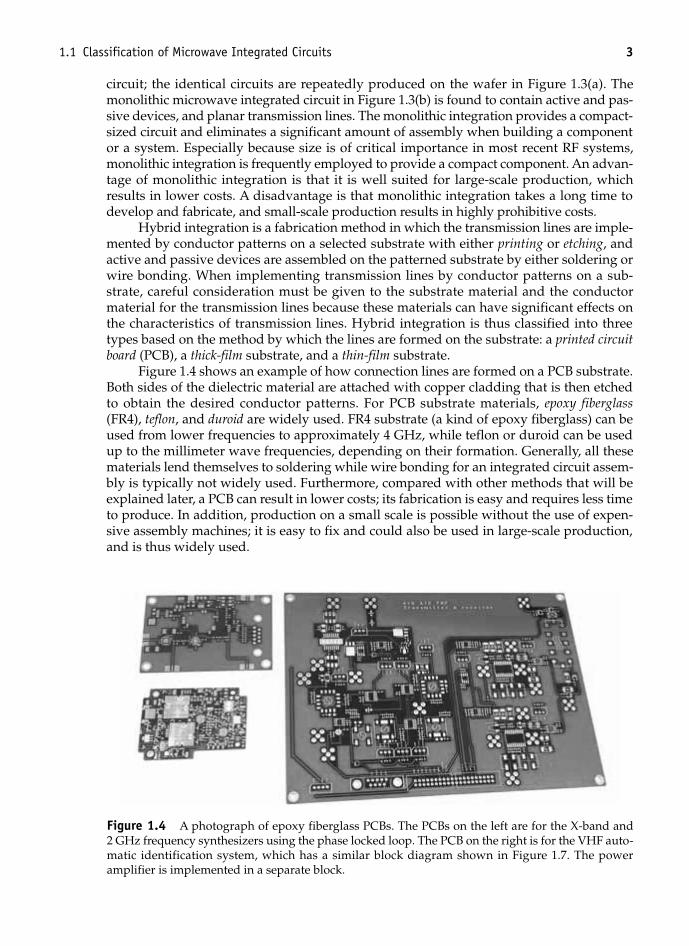
Figure 1.4 shows an example of how connection lines are formed on a PCB substrate. Both sides of the dielectric material are attached with copper cladding that is then etched to obtain the desired conductor patterns. For PCB substrate materials, epoxy fiberglass (FR4), teflon, and duroid are widely used. FR4 substrate (a kind of epoxy fiberglass) can be used from lower frequencies to approximately 4 GHz, while teflon or duroid can be used up to the millimeter wave frequencies, depending on their formation. Generally, all these materials lend themselves to soldering while wire bonding for an integrated circuit assem-bly is typically not widely used. Furthermore, compared with other methods that will be explained later, a PCB can result in lower costs; its fabrication is easy and requires less time to produce. In addition, production on a small scale is possible without the use of expen-sive assembly machines; it is easy to fix and could also be used in large-scale production, and is thus widely used.
figure1.4 A photograph of epoxy fiberglass PCBs. The PCBs on the left are for the X-band and 2 GHz frequency synthesizers using the phase locked loop. The PCB on the right is for the VHF auto-matic identification system, which has a similar block diagram shown in Figure 1.7. The power amplifier is implemented in a separate block.

4 Microwave Integrated Circuits
Thick-film substrates are produced by screen-printing techniques in which conduc-tor patterns are formed by pushing conductive paste on a ceramic substrate through a patterned screen and then firing printed conductor patterns. The substrate is called thick film because the patterns formed by such techniques are generally much thicker than those formed using thin-film techniques. As a benefit of using screen-printing techniques, mul-tiple screen printings are possible. Dielectric or resistor patterns can also be formed by similar screen-printing techniques using dielectric or resistor pastes. Using an appropriate order of multiple screen printings, it is also possible to form capacitors and resistors on the ceramic substrate. Since the ceramic substrate is more tolerant of heat, it is easy to assem-ble active devices in the form of chips. On the other hand, considering the lines and pat-terns formed by this process, the pattern accuracy of thick film is somewhat inferior compared to that of thin film. The costs and development time, on a case-by-case basis, are somewhere between those of the PCB and thin-film processes. Recently, however, the inte-gration based on thick-film technology has become rare because its cost and pattern accu-racy are between the PCB and thin-film technology, while thick film is widely used to build multifunction components. A typical example is the package based on LTCC (low-temperature co-fired ceramics) technology.1 Multilayer ceramics and structuring are pos-sible in LTCC technologies. Figure 1.5 shows a photograph of thick-film patterned substrates fabricated using the thick-film process.
figure1.5 A photograph of substrates fabricated by the thick-film process. Identical circuits can be arrayed for efficient production. This circuit is for the mobile communication VCO presented in Chapter 10.
1. Refer to Barry LTCC, LTCC Surface Mount T/R Module, at www.barryind.com.
The thin-film technique is very widely used in the fabrication of microwave circuits for military and microwave communication systems. In the case of the thin-film process, a similar ceramic substrate material used in thick film is employed, but compared to the thick-film substrate, a fine surface-finish substrate is used. The most widely used substrate is 99% alumina (Al2O3). Other substrates such as fused silica, quartz, and so on are possi-ble for conductor-pattern generation based on thin-film technologies. The pattern

1.1 Classification of Microwave Integrated Circuits 5
formation on the substrate is created with a photolithographic process that can produce fine tracks of conductor patterns similar to those in a semiconductor process. Since the thin-film substrate is also alumina as in the case of a thick-film substrate, the assembly of semiconductor chips using wire bonding is possible. Thin film compared with PCB and thick film is more expensive, and due to the requirement of fine tracks, a mask fabrication is necessary and the process generally takes longer. Passive components such as resistors and air-bridge capacitors can be implemented using this process. In addition, integrated circuits produced by the thin-film process require special wire bonders and microwelding equipment for assembly. Compared to the monolithic integration process, the thin-film process tends to be cheaper in terms of cost, but compared to MMIC, the assembled circuit using the thin-film patterned substrate is difficult to characterize precisely because of unknown or poorly described parasitic circuit elements associated with the assembly methods such as wire bonding and die attach. Before the emergence of MMICs (monolithic microwave integrated circuits), thin-film technology was the conventional method for building microwave-integrated circuits (MICs). Figure 1.6 is a photograph of thin-film cir-cuits fabricated with the thin-film technique.
figure1.6 A photograph of substrates produced by the thin-film process. From top left to bottom right, they are filter, phase shifter, power amplifier (presented in Chapter 9), path-switching circuit by assembly, power divider, and 50 Ω lines.
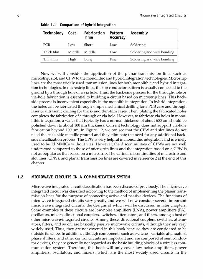
The choice of integration method depends on the application and situation, taking into account several factors mentioned previously, such as the operating frequency of the integrated circuit, the types of semiconductor components (chip or packaged), the forms of the passive components, large-scale fabrication costs, and method of assembly. These fac-tors should all be considered when selecting the optimum method of integration. For a description of microwave-patterned substrate fabrication, assembly with wire bonding and soldering, and packaging, see reference 1 at the end of this chapter. The book provides general information about microwave-circuit fabrications. Table 1.1 provides a comparison of the hybrid integrations described previously.
6 Microwave Integrated Circuits
Table1.1 Comparisonofhybridintegration
Technology Cost fabricationTime
PatternAccuracy
Assembly
PCB Low Short Low Soldering
Thick film Middle Middle Low Soldering and wire bonding
Thin film High Long Fine Soldering and wire bonding
Now we will consider the application of the planar transmission lines such as microstrip, slot, and CPW to the monolithic and hybrid integration technologies. Microstrip lines are the most widely used transmission lines for both monolithic and hybrid integra-tion technologies. In microstrip lines, the top conductor pattern is usually connected to the ground by a through hole or a via hole. Thus, the back-side process for the through-hole or via-hole fabrication is essential to building a circuit based on microstrip lines. This back-side process is inconvenient especially in the monolithic integration. In hybrid integration, the holes can be fabricated through simple mechanical drilling for a PCB case and through laser or ultrasonic drilling for thick- and thin-film cases. Then, plating the fabricated holes completes the fabrication of a through or via hole. However, to fabricate via holes in mono-lithic integration, a wafer that typically has a normal thickness of about 600 µm should be polished down to about 100 µm thickness. Current technology does not support via-hole fabrication beyond 100 µm. In Figure 1.2, we can see that the CPW and slot lines do not need the back-side metallic ground and they eliminate the need for any additional back-side metallization process. The CPW is very helpful in monolithic integration and is widely used to build MMICs without vias. However, the discontinuities of CPWs are not well understood compared to those of microstrip lines and the integration based on a CPW is not as popular as that based on a microstrip. The various discontinuities of microstrip and slot lines, CPWs, and planar transmission lines are covered in reference 2 at the end of this chapter.
1.2 MICROwAvE CIRCuITs InA COMMunICATIOn sysTEM
Microwave integrated circuit classification has been discussed previously. The microwave integrated circuit was classified according to the method of implementing the planar trans-mission lines for the purpose of connecting active and passive devices. The functions of microwave integrated circuits vary greatly and we will now consider several important microwave integrated circuits, the designs of which will be discussed in later chapters. Some examples of these circuits are low-noise amplifiers (LNA), power amplifiers (PA), oscillators, mixers, directional couplers, switches, attenuators, and filters, among a host of other microwave-integrated circuits. Among these, directional couplers, switches, attenu-ators, filters, and so on, are basically passive microwave circuits, although they are very widely used. Thus, they are not covered in this book because they are considered to be outside its scope. In addition, although components such as switches, variable attenuators, phase shifters, and other control circuits are important and are composed of semiconduc-tor devices, they are generally not regarded as the basic building blocks of a wireless com-munication system. Therefore, this book will only cover low-noise amplifiers, power amplifiers, oscillators, and mixers, which are the most widely used circuits in the

1.2 Microwave Circuits in a Communication System 7
construction of wireless communication systems. The basic design theory of these circuits as well as the devices related to them will be explained in this book.
As an example of a wireless communication system, Figure 1.7 shows a block dia-gram of an analog cellular phone handset (Rx frequency is 869–894 MHz and Tx frequency is 824–849 MHz).2 A general transceiver used for the transmission and reception of analog signals (usually voice) has a similar block diagram that is shown in Figure 1.7. A weak RF signal with a typical power level of about −100 dBm (0.1 nW) received from an antenna first goes through a filter called a diplexer and the signal is received only in the receiver frequency band. The filtered signal is too weak for direct demodulation or signal process-ing, and a low-noise amplifier (LNA) with a gain of 20–30 dB is required to amplify the received signal. Too much gain may cause distortion and an LNA with a gain of 20–30 dB is usually employed. Chapter 8 provides a detailed explanation of the design of an LNA.
Next, because the received signal frequency is so high, the first mixer shown in Fig-ure 1.7 translates the carrier frequency to a lower frequency band called first IF (intermedi-ate frequency). A double-conversion superheterodyne receiver is more widely used than a single-conversion super heterodyne receiver in a communication system. The filter in front of the first mixer again suppresses both the image frequency signal and other signals at the outside of the receiving frequency band. Since multiple users in service are using the same frequency band, multiples of other user signals generally coexist with the signal in the first
figure1.7 A block diagram of an analog mobile phone handset (AMPS standard). Tx_EN stands for Tx enable and ALC stands for automatic level control. Tx_ and Rx_data are required to set the programmable frequency dividers in Tx and Rx synthesizers. LE stands for Load Enable. When LE is high, the digital channel data are loaded to the corresponding programmable frequency divider in PLL IC. Synthesizers are explained in Chapter 11. Lock signal indicates that the synthesizer using PLL is in a locked state.
2. Refer to AMPS (Advanced Mobile Phone System) standard.

8 Microwave Integrated Circuits
IF. Intermodulations among the multiple signals are one of the crucial issues in mixer design. Chapter 12 describes the typical topologies of various mixers for suppressing such spurious signals. In order to filter out possible spurious signals that appear at the first mixer output, the signal is passed through a narrow bandpass filter that has a bandwidth of about the signal bandwidth. The first IF filter removes many unwanted spurious signals although it may not be completely sufficient. The first IF output is converted again through the second mixing. Now the center frequency of the second IF is low enough, the highly selective filter is available, and the spurious signals can be sufficiently suppressed through the second IF filter. In addition, the signal frequency is low enough and can be demodu-lated for the recovery of the original signal. The demodulator is an FM demodulator and is almost the same as the FM demodulator that is commercially popular.
Note that the mixer requires the input signal from a local oscillator (LO) for the transla-tion of the signal frequency to the IF. The two LO signals are supplied from the two Rx-synthesizers and each Rx-synthesizer consists of a voltage-controlled oscillator (VCO) and a commercial PLL (phase-locked loop) IC (integrated circuit). Since the frequency of most VCOs is not stable enough to be used in such communication systems, the frequency of a VCO must be stabilized using a stable crystal oscillator (XO in Figure 1.7) with a typical temperature stability of 2 ppm (parts per million) and a phase-locked loop (PLL). Further-more, the LO frequency should be moved up and down according to the base station com-mands. Such frequency synthesis and stabilization can be achieved by a phase-locked loop (PLL). To build a frequency synthesizer using PLL, the VCO frequency as well as the crystal oscillator frequency must be divided by appropriate programmable frequency dividers in the PLL IC. The signals CLK, Rx_ChDATA, Rx_ChLE, and Rx_Lock, shown in Figure 1.7, are the digital signals between the PLL IC and the system controller. The clock signal CLK is used for the timing reference signal that is generated by the system controller using the crystal oscillator. Rx_ChDATA sent from the controller represents the digital data to set the programmable frequency dividers. The signal Rx_ChLE selects the corresponding pro-grammable divider for Rx_ChDATA to be loaded among several frequency dividers in the PLL IC. When phase lock is achieved, the PLL IC sends the signal Rx_Lock to the system controller to inform the phase lock completion. The two Rx synthesizers are necessary for the double-conversion superheterodyne receiver. The commercial PLL IC generally includes the necessary components to achieve the phase lock for two VCOs in a single PLL IC. Thus, the LO signal for the second conversion is similarly synthesized using a single PLL IC. The design of the Tx and Rx VCOs in Figure 1.7 as well as the other microwave VCOs are described in Chapter 10, while the PLL’s operation is explained in Chapter 11.
In the transmission operation, the modulation input signal (usually voice) goes to the modulation input of a Tx synthesizer. The Tx synthesizer is similarly composed of a VCO and a PLL IC. Through the PLL IC, the desired carrier center frequency is similarly synthe-sized as in the Rx synthesizer. The digital signals CLK, Tx_ChDATA, Tx_ChLE, and Tx_Lock are similarly interpreted as in the Rx synthesizer. The modulation signal has a generally higher frequency than the PLL loop bandwidth and thus can modulate a VCO without the effects of a PLL. Therefore, the frequency-modulated (FM) signal appears at the Tx synthesizer output with the synthesized carrier frequency. The modulated signal then passes through the bandpass filter that removes unnecessary or spurious signals. The average output power level of the modulated signal is generally low; thus, in order to obtain the desired RF power output level, the signal must be amplified by a power ampli-fier (PA) whose typical maximum output power level is about 1W. The function ALC (Automatic Level Control) is generally built in to control the transmitting power level. When a user is close to the base station, the transmitting power level is set to low;
1.3 Summary 9
otherwise, it is set to high for a better quality of communication. The PA output signal is then passed through a diplexer without affecting the receiver and radiated via the antenna. A power amplifier is important in this type of communication system because it consumes most of the DC power supplied from a battery. Furthermore, because a power amplifier operates in large-signal conditions, significant distortion arises. In Chapter 9, we will dis-cuss the design and linearity evaluation of a power amplifier.
Given the preceding discussion, the key circuits in building a communication system are a low-noise amplifier, a power amplifier, oscillators, and mixers. With that in mind, this book will discuss in detail the design and evaluation method of these circuits.
1.3 suMMARy
• Microwave integrated circuits can be classified according to the fabrication method of the patterned substrate and in terms of monolithic and hybrid integration. Hybrid integration can be further classified into integrations based on PCB, thick film, and thin film. In the selection of integration, one type cannot be said to be superior to the other; the choice is made depending on the application and given situation, and by taking into consideration several factors such as cost, time, pattern accuracy, and assembly.
• Among active microwave circuits, the most commonly used building blocks for wire-less communication systems or other systems, such as repeaters, transponders, and radars, are amplifiers, oscillators, and mixers.
R E f E R E n C E s
1. T. S. Lavergetta, Microwave Materials and Fabrication Techniques, Dedham, MA: Artech House, Inc., 1984.
2. K. C. Gupta, Microstrip Lines and Slot Lines, 2nd ed. Dedham, MA: Artech House, Inc., 1996.
P R O b l E M s
1.1 A waveguide generally has lower line loss than a microstrip. An SIW (substrate inte-grated waveguide) can be considered as the planar version of a waveguide. How is an SIW configured using a substrate?
1.2 Find the TR (transmission and receiving) module example built using a LTCC on the Web site www. barryind.com.
1.3 How is the ALC in Figure 1.7 constructed? 1.4 Refer to the FM demodulator IC SA605, which is used to demodulate an FM signal.
Explain how the FM signal is demodulated using its block diagram. 1.5 Refer to the Web site of vendors of PLL IC such as Analog Devices Inc. or other com-
panies. Explain the synthesizer data bus shown in Figure 1.7. 1.6 How can the PLL be modulated? Explain how to set the PLL loop bandwidth by tak-
ing the bandwidth of a bandlimited modulation signal into consideration.

This page intentionally left blank

This page intentionally left blank

759
Numbers0.33-uF-chip tantal capacitors, 5651-dB compression points
of amplifiers, generally, 351–352in cascaded structures, 729–735conversion loss and, 640–642
1 pF broadband 0603 type 500S, 343
1608 chip resistors, 16, 256–2572-bit counters, 60328V pulse inputs, 1372SC4226 transistors, 5383-dB bandwidth, 10750 W (ohm)
amplifier source/load at, 279–280, 311
conductance circles at, 221–222dielectric resonator oscillators
at, 564–568, 573internal resistance at, 286matching circuits at, 327power dividers and, 71–72reference impedance at, 429resistors, 130, 174source/load impedance at, 322stability of circuits at, 335–336VCOs at, 546–548
8–12 GHz frequency band (X-band), 314
8510 Network Analyzer, 89
AA-counters, 602–603ABCD parameters, 113, 466AC
circuit simulations in, 237–239input/output connectors
in, 261small-signal analysis in, 238steady state in, 237
Accumulators, 603ACPRs (adjacent channel power
ratios). See Adjacent channel power ratios (ACPRs)
Active DC bias circuits, 176–177
Active devicesATF-36077, 314BJTs. See Bipolar junction
transistors (BJTs)DC bias circuits in, 173–180extraction of equivalent circuits,
181–195FETs. See Field effect transistors
(FETs)GaN HEMTs in, 356–359introduction to, 149–151large-signal, 314–315, 351–353LDMOSFETs in, 360–361LNAs. See Low-noise amplifiers
(LNAs)PAs. See Power amplifiers (PAs)problem exercises on, 196–200references on, 196small-signal, 351–353summary of, 195
Active loop filters, 612Active Snap Modes, 254Adaptive simulation
frequency, 274Additive theorem of
trigonometric functions, 508Adjacent channel power ratios
(ACPRs)calculation of, 445–446introduction to, 434, 440in linearity in PAs, 446–452predistorters and, 458–460
Admittancein equilibrium conditions,
487–488matrix of, 711in oscillation conditions,
482–486in parallel feedback
oscillators, 522ADS (Advanced Design System)
AC simulations in, 238–239auto-layout utility in, 336, 339characteristic impedance in, 43,
47–49
circuit simulations in, 230Class-D PAs in, 388common emitter amplifiers in,
250–251components in, 256–264DC simulations in, 230–234DC supply circuits in, 330–333DesignGuide in, 626–630Doherty PAs in, 469double-balanced mixers in,
698–699effective permittivity in, 47–49equilibrium conditions in, 488fourth-order loop filters in,
624–625Grid settings in, 253–254half-wave current sources
in, 381HB simulations in, 241–243HB1Tone_LoadPull.dsn of
examples in, 372–373ideal transmission line in, 37impedance-based start-up
conditions in, 487–491L-type matching circuits in,
210–211large-signal admittance of
diodes in, 741large-signal ports in, 98large-signal reflection
coefficients in, 743Layer Editor in, 250–253Layout Units in, 253–254load-pull simulation in, 365loop filter synthesis in, 626–627low-noise amplifiers in,
314–319, 336–345Main window in, 229–230matching circuit design in,
322–329mixer isolation in, 644–645Murata capacitor library
in, 24negative resistance in, 748noise parameters in, 127–133
Index

760 Index
ADS (Advanced Design System) (continued)
optimization controller in, 246–247
oscillation conditions in, 481, 752–754
OscPort in. See OscPortOscTest in. See OscTestOutline settings in, 254–256parallel feedback oscillators
in, 522PDF functions in, 446phase-locked loops in, 625–633phase noise simulation in,
627–630phasors in, 382p-shaped equivalent circuits
in, 74S-parameter simulation in, 98–99single-balanced mixers in, 689single-ended mixers in, 671–672single-stub tuners in, 221–222sm_gamma1(S)/sm_
gamma2(S) in, 305source/load impedances in,
319–321stability of amplifiers in, 333–336third-order loop filters in,
620–622transient responses in, 630–633transient simulation
components in, 234TriQuint and, 410two-tone measurements in,
448, 451VCO design in, 546, 550VCVS in, 459
AGC (automatic gain control), 676Agilent Technologies
E5052A signal source analyzers by, 570–571, 574–575
E8358A network analyzers by, 568–569
Air-filled microstrip lines, 45–46ALC (Automatic Level Control), 8AlGaN/GaN heterojunctions,
357–358Alumina, 267–268AM (amplitude modulation),
506–508American Technology Company
(ATC), 343
Amplifierscascaded, 133–136dielectric resonator oscillators
in, 565–568Doherty, 455, 463–473emitter, 250, 537feedforward, 461–462HMC313, 565–566low-noise. See Low-noise
amplifiers (LNAs)parametric, 149power. See Power amplifiers
(PAs)in VCOs, 537
Amplitude modulation (AM), 506–508
AnsoftClass-F PAs and, 412dielectric resonator oscillators
by, 568, 574matching circuit simulations
and, 427, 430APC-7, 158Application of transmission lines.
See also Transmission linesimpedance inverters in, 70–71introduction to, 60resonant transmission lines in,
60–69short-length transmission lines
in, 60two-port circuits in, 69–77two-port lumped-element
equivalent circuits in, 71–75
Arc Resolution fields, 272Array indices, 645–652ASCII text files, 140ATC (American Technology
Company), 343ATF-36077 transistors,
314–316, 338Attenuators, 121–122Auto-layouts, 248, 336, 339Automatic gain control
(AGC), 676Automatic Level Control
(ALC), 8Available
gain circles, 308power, 203power gains, 286, 289, 311–312
BBalanced signals, 684–685, 694Baluns, 684–685, 692–695, 699–703Band-gap parameters, 356–357Bandwidth (BW)
3-dB, 107in double L-type matching
circuits, 217output powers within, 451–452in phase-locked loops, 586–587resolution, 506–507, 511source/load resistance ratios
and, 209in T-type matching circuits, 215video, 506
Barkenhausen Criterion, 501Base-emitter (BE) junctions, 162,
164–169Base-spreading resistance, 164Baseband signal modulation,
434–438Basic oscillator circuits. See
Oscillator circuitsBasis functions, 266BCX19 BJTs, 149–150BE (base-emitter) junctions, 162,
164–169Beam lead packages, 656–657BERs (bit error rates), 434, 453Bessel function, 740Bipolar junction transistors
(BJTs)chip component layout in, 257DC bias circuits in, 173–177GaAs/AlGaAs HBTs, 172–173introduction to, 149–151large-signal model of, 165–168packages of, 171S-parameters and, 168–171,
179–180Si, 149–150, 162–164simplified equivalent circuits
and, 168–171Bit error rates (BERs), 434Bit rates, 434–436Bits, 437–438, 441–442BJTs. See Bipolar junction
transistors (BJTs)Blocks, 248Bode plots, 620–621Boltzmann, Ludwig, 130Bonding ribbons, 412
Index 761
Bonding-wire inductance, 159–160, 657
Boolean Logical Operation, 260Branch, 419–420Branch-line couplers. See also
Coupling, 457Breakdown voltage, 356Broadband matching circuits, 219BW (bandwidth). See Bandwidth
(BW)
CCAD simulators, 512, 560Calibration, defined, 104–105Capacitance
in GaAs FET packages, 161in large-signal GaAs
MESFETs, 154in small-signal GaAs MESFETs,
152–153in transmission lines, per unit
length, 31–32, 39Capacitors
chip. See Chip capacitorsin matching circuit simulations,
428–429as passive devices, generally,
11–16in RF decoupling, 175–176in VCOs, 536–538
Carrier frequency, 507–508Carriers, 439–440Cascade101.xls, 733Cascaded amplifiers, 133–136Cascaded structures, 729–735CB (collector-base) junctions,
162–169CDMA (code division multiple
access), 450–454, 460–463Cds, 190CE_Amp_Layout windows,
262–263Cells, 266Cellular phones
introduction to, 7–9VCOs for. See Voltage-
controlled oscillators (VCOs)
Center frequency, 507–508Ceramic packages, 657Cgs/Cgd, 190Channel formation, 150
Characteristic impedance. See also Impedance, 37–39
Charge pumps, 596, 611, 616Chip capacitors
0.33-uF-chip tantal, 565High-frequency chip DC block,
330–331introduction to, 16–18in PAs, 363–364in VCOs, 536–538
Chip-type componentscapacitors. See Chip capacitorsdiodes, 672FETs, 190–193GaAs FETS, 157inductors, 19–21passive components, generally,
12–14resistors, 21–22
Circuit boards, 534–535Circuit simulation. See also
CircuitsAC, 237–239in ADS, 227–230amplifier fabrication/
measurement in, 337, 343–345
classification of, 230DC, 230–234harmonic balance, 239–243layout and. See Layoutmatching circuits in, 340–341Momentum for. See Momentummulti-tone harmonic balance,
243–246optimization in, 246–247source inductors in, 338–339transient, 234–237
CircuitsDC-bias. See DC bias circuitsequivalent. See Equivalent circuitsfeedback, 523–524, 560–561half-wave rectifier, 242load. See Load circuitslogic, 592–594matching. See Matching circuitsMICs. See Microwave
integrated circuits (MICs)MMICs. See Monolithic
microwave integrated circuits (MMICs)
oscillator. See Oscillator circuits
parallel resonant, 557–558PCBs. See Printed circuit boards
(PCBs)self-bias, 178shunt stabilizing, 317–318simulation of. See Circuit
simulationtwo-port, 523–524
CITI (Common Instrumentation Transfer and Interchange), 140, 142
Class-A power amplifiers (PAs), 355, 374–375
Class-AB/B/C operating points, 376–377
Class-B power amplifiers (PAs), 377–385, 464–466, 469–473
Class-C power amplifiers (PAs), 377–385, 464–467, 469–473
Class-D power amplifiers (PAs), 386–390
Class-E power amplifiers (PAs), 390–398
Class-F power amplifiers (PAs)design example of, 410–412input/output impedances in,
412–418input/output matching circuits
in, 418–424introduction to, 398–409matching circuits using EM
simulation in, 424–432Classification
of circuit simulations, 230of microwave integrated
circuits, 1–6of passive devices, 12–15of power amplifiers, generally,
374–377Closed-loop
dielectric resonator oscillators, 562–563
gains, 606–609transfers, 584–585
CMOS (Complementary MOS), 151Co-planar waveguide (CPW),
1–2, 6Coaxial transmission lines. See
also Transmission linesadaptors for, 42characteristic impedance of, 40,
43–44

762 Index
Coaxial transmission lines (continued)
connectors for, 41–42introduction to, 2phase velocity of, 40
Code division multiple access (CDMA), 450–454, 460–463
Cold-FET measurements, 191–193Cold states, 136–138Collector-base (CB) junctions,
162–169Collector efficiency, 354–355Collector voltage
in Class-D PAs, 386in Class-E PAs, 391, 395–397in Class-F PAs, 399–401, 407–409in GaN HEMTs, 356
Colpitts oscillatorscircuits in, 522, 525introduction to, 504–505negative resistance in, 744–751oscillation conditions in, 755–757
Common Instrumentation Transfer and Interchange (CITI), 140, 142
Communications systems, defined, 6–9
Comp layer, 249Comparison signals (SIGs),
592–595Complex-valued source/load,
217–219Component Library, 262Components, in layouts, 248–249Composite PAs. See also Power
amplifiers (PAs)Doherty, 462–473EER in, 462feedforward, 461–462introduction to, 455predistorters in, 455–460
Compression points, 646–647Cond layer, 269Conductance, 489–490Conduction
angles, 376band energy, 658in Class-B/Class-C PAs, 384–385
Conic sections, 745–747Conjugate matching
of amplifier input/output, 203–204
gains and, generally, 311–312
in low-noise amplifiers, 292, 301–306
power gains and, generally, 291–292
Connectors, 42–43Constant-conductance circles
in L-type matching circuits, 209–210, 213
in single-stub tuners, 220–221Constant-resistance circles,
209–210, 213Constellation plots
baseband signals and, 435–437envelope simulation and,
442–444EVM simulation and, 454
Contour plots, 372–374, 415Conversion impedance matrix,
713–715Conversion loss (CL)
in double-balanced mixers, 698–699
mixer isolation and, 645–646mixer types and, 703in mixers, generally, 640–642,
703, 714–720in SBMs, 688–689, 696in Schottky diodes, 664in SEMs, generally, 667, 673in SEMs using diodes, 668,
670–672in SEMs using transistors, 675
Coordinate Entry windows, 255–258, 260
Coplanar strip (CPS) transmission lines, 684–685
Copper plates, 248Copy Relative pop-up
windows, 259Corner discontinuities, 78–79Coupling
branch-line couplers for, 457in dielectric resonator
oscillators, 560–562directional couplers for, 88DRs to microstrips, 555–562loops, 69RF decoupling vs., 174–176
CPS (coplanar strip) transmission lines, 684–685
CPW (co-planar waveguide), 1–2, 6
Cree, Inc., 358
Crests, 35Cross junctions, 79–80Crystal oscillators
introduction to, 581–582phase-locked loops in, 585phase noise and, 514–515,
598–599Current
characteristic impedance and, 37–38
phase velocity of, 30–32in two-port networks, 90
Curtice model, 155Curtis, J., 513Cut-off frequency, 665
DD-ports (out-of-phase distribution
ports), 685, 690–692DACs (data access components),
410–411DACs (digital-to-analog
converters), 441Damping ratio, 607Data access components (DACs),
410–411Data devices, 140Data directory, 227–228, 273–276Dataset fields, 274dB (decibels). See Decibels (dB)DBMs. See Double-balanced
mixers (DBMs)DC bias circuits
active, 176–177in bipolar junction transistors,
173–177in dielectric resonator
oscillators, 567in field effect transistors,
177–180introduction to, 173in PAs, 363, 374–377RF decoupling and, 174–176S-parameter simulation and,
178–180simulation of, 230–234in VCOs, 546–548, 552
DC block capacitorsin bipolar junction transistors,
174–175in Colpitts oscillators, 525in dielectric resonator
oscillators, 566–567

Index 763
EM simulations and, 550oscillating transistors and, 538parallel resonant circuits and,
489–490in VCO load circuits, 546–548
DC voltage. See also Voltagein Class-B/Class-C PAs,
377–383in Class-D PAs, 386–389in Class-E PAs, 391–395in EER, 462in low-noise amplifiers, 330–333in Schottky diodes, 661–663in single-ended mixers, 670supply terminals for, 259in VCOs, 536
*.dds (display data file), 229Decibels (dB)
in cascaded structures, 729–735defined, 727–729Frii’s formula and, 134–136
Delivered power, 97–98Depletion
capacitance, 168, 660–661, 710channels, 150FETs, 177
Designof Class-F PAs. See Class-F
power amplifiers (PAs)of discrete matching circuits,
217–219of double-balanced mixers,
699–703of DROs. See Dielectric
resonator oscillators (DROs)of low-noise amplifiers. See
Design of LNAsof SBMs using diodes, 690–692of SBMs using transistors,
692–694of SEMs using diodes, 690–692of SEMs using transistors,
692–694Design of LNAs. See also Low-
noise amplifiers (LNAs)active device models in, 314–315DC supply circuits in, 330–333device performance in, 315–319example for, generally, 314fabrication and, 336, 343–345load impedance in, 319–321lumped-element matching
circuits in, 322–325
matching circuits in, generally, 322–329, 340–342
measurements in, 333–336, 343–345
source impedance in, 319–321source inductors in, 338–339stability in, 333–336transmission-line matching
circuits in, 325–329DesignGuide, 626–630Detuning, 390Device performance, 315–319Devices under test (DUTs)
introduction to, 23noise figures in, 124, 136–140reference planes in, 88, 104–105
Dielectric-filled microstrip lines, 45–46
Dielectric Loss Tangent options, 267
Dielectric Permittivity options, 267
Dielectric resonator oscillators (DROs)
design of, generally, 560, 576introduction to, 67–68phase noise in, 514–515using feedback, components,
565–568using feedback, low phase
noise, 573–575using feedback, prototypes,
568–572using feedback, theory, 562–565using replacements, 560–562
Dielectric Resonators (DRs), 552–559
Dielectric Thickness options, 267Diffusion capacitance, 168Digital signal processing (DSP)
simulators, 453Digital-to-analog converters
(DACs), 441Diodes
approximating as on/off switches, 664–667
in double-balanced mixers, 694–700
forward-biased, 654Gunn, 149–151, 480–481, 525I-V characteristics of, 654–655IMPATT, 150–151, 480–481, 525MBD101, 689, 698
in mixers, generally, 639–640PIN, 149quads of, 699–700in SBMs, design of, 690–692in SBMs, generally, 685–689in SBMs, qualitative analysis of,
685–692Schottky. See Schottky diodesin SEMs, design of, 672–673,
690–692in SEMs, LO analysis of,
704–707in SEMs, qualitative analysis of,
664–672, 685–689in SEMs, quantitative analysis
of, 704in SEMs, small-signal analysis
of, 707–714space-charge-region, 165–167switching, 666–667varactor, 149, 539–540, 567–568
Directional couplers. See also Coupling, 88
Discontinuitiescorner, 78–79cross junctions in, 79–80open-end microstrip lines and,
76–78step, 78–79T-junctions in, 79in transmission lines,
generally, 76Discrete format files, 410Discrete matching circuits. See also
Matching circuitsdouble L-type, 216–217L-type, 207–212p-type, 212–214series-parallel conversion in,
205–207source impedance and, 217–219T-type, 214–216
Display data file (*.dds), 229Display windows
in ADS, 227–228efficiency in, 384load-pull simulation in, 371–374phase-locked loops in, 621
Doherty power amplifiers (PAs)Class-B, 464–466, 469–473Class-C, 464–467, 469–473introduction to, 455, 462–473
Doping, 360

764 Index
Double-balanced mixers (DBMs)design examples of, 699–703introduction to, 591, 640qualitative analysis of, 694–699using transistors, 700–703
Double L-type matching circuits, 216–217
Double-stub tuner matching circuits, 222
Drainin Class-B/Class-C PAs,
377–381in Class-D PAs, 386–389in Class-E PAs, 394in Class-F PAs, 409, 410–413, 420in Doherty PAs, 465–467efficiency, 354–355in GaAs FET packages, 160in large-signal GaAs MESFETs,
154–156in LDMOSFETs, 360–361in PA classification, 374–377in small-signal equivalent
circuits of FETs, 157in small-signal GaAs MESFETs,
152–153DRD107UC048 resonators, 568Drill layers, 258–260Drilling, 248–249DROs. See Dielectric resonator
oscillators (DROs)DRs (Dielectric Resonators),
552–559*.ds (dataset files), 227–229*.dsn (design files), 227–229DSP (digital signal processing)
simulators, 453Dual-gate FETs, 676–679Dual modulus counters, 601–602Duroid substrate, 3DUTs. See Devices under test
(DUTs)
EEarly effect, 166EEHEMT model, 410–412EER (envelope elimination and
restoration), 455, 462Effective dielectric constants, 46Effective permittivity, 46–49Efficiency
in Class-B/Class-C PAs, 384–385in Class-D PAs, 386–389
in Class-E PAs, 391–394, 397in Class-F PAs, 398, 401, 405–409in Doherty PAs, 467–468, 472
Electric fieldsin double-balanced mixers, 699in SBMs, 683, 691, 724in Schottky diodes, 660–661simulation of, 360–361
Electrical delay, 23Electrical length, 36–38, 60Electromagnetic (EM) simulation
introduction to, 15momentum for. See Momentum
Electromagnetic fields, 553Electron affinity, 658, 664Electron mobility
in GaAs MESFETs, 151in GaAs pHEMTs, 161–162in GaN HEMTs, 356–358in HEMTs. See HEMTs (high-
electron-mobility transistors)in LDMOSFETs, 360–361
Electron wells, 161EM simulation. See
Electromagnetic (EM) simulation
Emittersin BJT DC-biased circuits,
173–174in BJTs, generally, 162–165in Colpitts oscillators, 505,
522–525in GaAs HBTs, 172layout of, 250in VCOs, 536–5377
Enable Snap, 254Enamel-coated copper wires, 19Energy band-gap, 356–357Enhancement type channels, 150ENR (Excessive Noise Ratio),
136–139Ensembles, 114–115Entry/Edit options, 255, 263Envelope elimination and
restoration (EER), 455, 462Envelopes
elimination and restoration of, 455, 462
phasors as, 438–439simulation of, 439–446
Epitaxial layers (epi-layers), 152, 162–164
Epoxy fiberglass (FR4) substrates, 3
Equilibrium conditionsdefined, 479impedance-based, analyzing
with ADS, 487–491impedance-based, generally,
486–487open-loop gain-based,
500–506reflection coefficient-based,
generally, 492–494reflection coefficient-based,
implementing circuits, 494–496
reflection coefficient-based, large-signal, 496–499
Equivalent circuitsin DRs, 555extraction of. See Extraction of
equivalent circuitsFET small-signal, 352, 375–377GaAs FET simplified,
186–187large-signal, 154–156lumped, 31, 66Norton. See Norton equivalent
circuitsp-shaped, 72–75, 181–187in passive devices, 16reference planes and, 106–107in S-parameter simulations, 98simplified, 168–171small-signal, 157–159, 238T-shaped, 72–73, 181–183Thevenin, 282–285, 288two-port lumped, 71–75
Equivalent thermal noise resistance, 120
Ergodic processes, 115–117Error vector magnitude (EVM),
434–437, 453–454Etching, 3EVM (error vector magnitude),
434–437, 453–454Excel, 135Excessive Noise Ratio (ENR),
136–139Exclusive OR (XOR) phase
detectors, 592–594Experimental load-pull method,
362–364Expressions
of internal noise, 112–113of noise parameters, 124–133

Index 765
External noise sourcesexpression of noise parameters
and, 124–126noise figures and, 122–124representation of, 113–117
Extraction of equivalent circuitsDC simulation circuits in,
187–188in dielectric resonators,
557–559microstrip ring-type inductors
in, 183–185for passive devices, 183, 191physically modeled equivalent
circuits in, generally, 181p-type equivalent circuits in,
181–187S-parameter simulation in,
184–191simplified FET equivalent
circuits in, 186–191T-type equivalent circuits in,
181–183Extrinsic elements, 157, 191
FFabrication of LNAs. See also
Low-noise amplifiers (LNAs)
introduction to, 336matching circuits in, 340–342overview of, 343–345source inductors in, 338–339
FDM/FDMA (frequency division multiplexing), 434
Feedbackcircuits, 560–561DROs and. See Dielectric
resonator oscillators (DROs)networks, 500–503, 516–517,
528–529parallel feedback oscillators,
515–522series feedback inductors, 317series feedback oscillators. See
Series feedback oscillatorsTap and Seed method for, 441
Feedforward power amplifiers (FPAs), 461–462
Fermi energies, 658FETs. See Field effect transistors
(FETs)FHX35LG pHEMTs, 530
FHX35LG transistor packages, 544–546
Field effect transistors (FETs)cold, 191–193DC bias circuits in, 177–180dual-gate, 676–679GaAs MESFETs, 152–154, 358GaAs pHEMTs, 151, 161–162Intrinsic, 193introduction to, 150, 151large-signal equivalent circuits
in, 154–156LDMOSFETs, 360–361Leeson’s phase noise model
and, 513nonlinear, 666packages and, 159–161resistive operations in, 675S-parameters and, 157–159simplified equivalent circuits
in, 186–187single-gate, 676–678small-signal equivalent circuits
in, 157–159, 352, 375–377Field-shape matching, 201–202File formats, 140–142File managers, 228–229Fin-line single-balanced mixers
(SBMs), 691First IFs (intermediate
frequencies), 7–8Fixed frequency dividers, 601Flexible cables, 42FM (frequency-modulated)
signals, 8, 513Focus Microwaves Inc., 363Forward-biased diodes, 654Forward-biased junctions,
162–163, 165–166Forward/reverse operations,
661–663Four-diode pairs, 699–700Four-port linear networks, 704Fourier series
Class-F PAs in, 402Doherty PAs in, 470drain current in, 674envelope waveforms in, 440half-wave current sources in,
381–382harmonic balance simulations
in, 240–241IF output waveform in, 687
mixer operations in, 667noise signal analysis in, 117–119PA classification in, 376single-ended mixers in, 669transconductance in, 674voltage/current relationship
in, 706Fourier transformations, 117, 244Fourth-order loop filters, 624–625FPAs (feedforward power
amplifiers), 461–462FR4 (epoxy fiberglass)
substrates, 3Fractional frequency dividers,
603–605FreeSpace, 267Frequency
adaptive simulation, 274carrier, 507–508center, 507–508characteristic impedance and,
37–40in chip-type capacitors, 17–18in chip-type inductors, 19–21in chip-type passive
components, 22–26cut-off, 665in decibels, 728–729down-converted terms,
639–640in DRs, 557–559in higher-order loop filters,
617–622indices, 245–246intermediate, 7–8jitters, 581linear simulation, 274logarithmic simulation, 274in phase-locked loops, 608–609resolution, 118single-point simulation, 274transmission line length and,
36–37transmission lines and,
generally, 29–30tuning, 541–543, 564, 571–572up-converted terms, 639–640
Frequency-dependent load reflection coefficients, 367
Frequency dividersin loop filter design, 629phase-locked loops in, 590,
600–605
766 Index
Frequency division multiplexing (FDM/ FDMA), 434
Frequency-modulated (FM) signals, 8, 513
Frequency synthesizersintroduction to, 582phase-locked loops in, 587–589,
612–615, 619Frii’s formula, 133–136, 314Fringing capacitance, 47Fukui method, 192Fusing currents, 424
GGaAs/AlGaAs HBTs, 172–173GaAs (gallium arsenide) MESFETs
GaN HEMTs and, 358introduction to, 150–154large-signal equivalent circuits
in, 154–156Leeson’s phase noise model
and, 513packages of, 159–161pHEMTs and, 151, 161–162S-parameters and, 157–159simplified equivalent circuits,
186–187small-signal equivalent circuits
in, 157–159Gains
ATF-36077, 315–316available power, 289in cascaded structures,
729–730, 735circles, 306–308, 312–313in Class-F PAs, 417–418, 424in DC supply circuits, 333in dielectric resonator
oscillators, 566input/output reflection
coefficients in, 281in low-noise amplifier
fabrication, 343–345lumped-element matching
circuits and, 322–325margins in, 616in matching circuit simulations,
342, 431–433in PDAs, 460power, 286–287, 290–291summary of, 311–312Thevenin equivalent circuits in,
282–285
transducer power, 287–289transmission-line matching
circuits and, 329unilateral power, 291–292
Gallium arsenide (GaAs) MESFETs. See GaAs (gallium arsenide) MESFETs
Gallium nitride. See GaN (gallium nitride)
Gamma propagation constant, 275GaN (gallium nitride)
in Class-F PAs, 410–412heterojunctions, 357–358high-electron-mobility
transistors, 356–359, 410–412semiconductors, 357–358
Gatesin Class-F PAs, 411–413in large-signal GaAs
MESFETs, 154in small-signal equivalent
circuits of FETs, 157in small-signal GaAs MESFETs,
152–153Gauss law, 119, 660Gerber format files, 248Gibb’s phenomenon, 389, 402Gilbert cells, 700–703Global variables, 239gm, 190GND, 267Green’s function, 264–268Grid/Snap options, 253–254Grids, 248–249Ground points, 505, 524Group delay
in DROs, generally, 564–565in low phase noise DROs,
573–575in prototype DROs, 568–571
Gummel plots, 166–167Gunn diodes, 149–151, 480–481, 525
HH-states, 594–596Half-wave current sources
in Class-B PAs, 381–384in Class-E PAs, 398in Class-F PAs, 407–409in Doherty PAs, 466, 469–471
Half-wave rectifier analysis, 736–738
Half-wave rectifier circuits, 242
Half-wave waveformsin Class-B PAs, 382–384in Class-E PAs, 398
Half-wavelength transmission lines
application of, generally, 60, 63–64
defined, 36in reflection and return loss, 54in two-port circuits, 69
Handy-reformable cables, 42Harmonic balance
in Class-D PAs, 388–390in Class-E PAs, 396in Class-F PAs, 416–417, 423in Doherty PAs, 469–471EM simulations and, 551in equilibrium conditions, 490in feedback oscillators, 530–533half-wave rectifier analysis for,
736–738in load-pull simulations,
365–367in matching circuit
simulations, 432in mixer conversion loss, 645in mixer simulations, 647in oscillation output power, 499in PDAs, 459simulation of. See Harmonic
balance simulationsweep and, 368–370, 373–374in VCOs, 542
Harmonic balance simulationintroduction to, 440, 444linearity in PAs in, 448multi-tone, 243–246OscPort and, 491, 497overview of, 239–243
Harmonic impedancein Class-F PAs, 414–419in load-pull simulations, 366in PAs, generally, 362–363sweep and, 374
Harmonicsin Class-F PAs, 400–409, 418filters eliminating, 389–390
HB1Tone_LoadPull.dsn of examples, 372–373
HB.freq, 716–717HBTs (heterojunction bipolar
transistors), 172–173, 355–356

Index 767
HEMTs (high-electron-mobility transistors). See also Pseudomorphic HEMTs (pHEMTs), 151, 410–412
Heterojunction bipolar transistors (HBTs), 172–173, 355–356
HFSSfor Class-F PAs, 412for dielectric resonator
oscillators, 568for low phase noise DROs, 574in matching circuit simulations,
427, 430High-electron-mobility transistors
(HEMTs). See also Pseudomorphic HEMTs (pHEMTs), 151, 410–412
High-frequency chip DC block capacitors, 330–331
High impedance states, 595Higher-order loop filters, 616–625Highly doped region (N + Drain),
360–361Hittite, 565HMC313 amplifiers, 565–566Hot states, 136–138Hybrids, 2–6, 681–685
II-V characteristics of diodes,
654–655IC-CAP files, 140ICs (integrated circuits). See
Integrated circuits (ICs)IFs. See Intermediate frequencies
(IFs)IMD3 (third-order
intermodulation distortion)in FPAs, 461–462in matching circuit
simulations, 434in mixers, 641–642in PAs, 447–448in PDAs, 460
IMPATT diodes, 150–151, 480–481, 525
Impedanceanalyzers of, 22–26characteristic, 37–39conversion impedance matrix,
713–715equilibrium conditions based
on, 486–491
high impedance states, 595input/output, 412–418inverters. See Impedance
inverterslarge-signal, 739–743load. See Load impedancematching. See Impedance
matchingin matching circuit
simulations, 429in passive devices, 11–12, 22–26reference, 88, 92, 751in reflection and return loss,
53–54start-up conditions based on,
481–491Z0, 275–276
Impedance invertersintroduction to, 54matching circuits and, 223–224for transmission lines, 70–71
Impedance matchingDC supply circuits in, 330–333discrete matching circuits in.
See Discrete matching circuits
impedance inverters and, 223–224
introduction to, 201–202lumped-element matching
circuits in, 322–325maximum power transfer
theorem in, 202–204problem exercises on, 225–226references on, 224–225single-stub tuners in, 219–223summary of, 224transmission-line matching
circuits in, 219–224, 329Impulse response, 437–439Impurity scattering, 161In-phase distribution ports
(S-ports), 685, 690–692Incident voltages, 88–89, 99–105Incident waves, 52, 90–91indep(m3)/indep(m4), 25Inductance
in GaAs MESFETs, 160per unit length, 31, 39, 46
Inductors, 11–16Inphase and quadrature-phase
(IQ) modulation, 435–437Input matching circuits, 421–424
Input/output impedance, 412–418
Input/output reflection coefficients, 281
Insertiongain, 108–110loss, 565–566, 574technique for, 13
Instances, 248Integer frequency dividers,
603–605, 617Integrated circuits (ICs)
introduction to, 8microwave. See Microwave
integrated circuits (MICs)monolithic microwave. See
Monolithic microwave integrated circuits (MMICs)
Interdigital capacitors, 425–426Intermediate frequencies (IFs)
introduction to, 7–8mixer isolation and, 642–652in mixers, generally, 639–642
Internal noise sourcesexpression of, 112–113noise figures and, 122–124
Intersymbol interference (ISI), 437Intrinsic FETs. See also Field effect
transistors (FETs), 193IQ (inphase and quadrature-
phase) modulation, 435–437, 441–442, 454
ISI (intersymbol interference), 437Isolation of mixers, 642–652, 703
JJohnson, John B., 119
KKahn EER technique, 462Kelvin, 119Kirk effect, 166Korea, 451KOVAR, 657
LL-type matching circuits
in Class-F PAs, 421double L-type, 216–217overview of, 207–212
Land patterns, 13Laplace transforms, 583,
607, 610

768 Index
Large-signal conditionsactive devices in, 314–315,
351–353admittance in, 739–743BJTs in, 165–168equilibrium conditions in,
480, 496equivalent circuits in, 154–156FHX35LG pHEMTs in, 544GaAs MESFETs in, 154–156impedance in, 739–743ports in, 98simulations in, 541–542, 551
Laterally diffused MOSFETs (LDMOSFETs), 356, 360–361
Layer Editor, 250–252Layers, 248–249Layout
automatic, 336, 339components in, 256–264, 550Grid settings in, 253–254introduction to, 248–250layers in, 250–253, 267–269manual, 248–250Momentum for. See MomentumOutline settings in, 254–256problem exercises on, 277–278references on, 276Schematic/Layout window in,
227–228summary of, 276units in, 249, 253–254
LDMOSFETs (laterally diffused MOSFETs), 356, 360–361
LE (Load Enable), 7Lead-type passive components,
12–14Least significant bits (LSBs),
441–442Leeson’s phase noise model,
509–513, 565Length of transmission lines. See
also Transmission linescharacteristic impedance and,
37–40phase velocity and, 30–35wavelength and, 35–37
LG (low parasitic, hermetically sealed metal-ceramic package), 544–546
Lightly doped regions (NHVs), 360–361
Linear circuit analysis. See also Nonlinear circuit analysis
in AC simulations, 238in DC simulations, 231–234in transient simulations,
235–237Linear simulation frequency, 274Linearity
circuit analysis in. See Linear circuit analysis
in FPAs, 462in PAs. See Linearity in PAsin PDAs, 460in predistorters, 455–456in simulation frequency, 274in two-tone measurements, 450
Linearity in PAs. See also Power amplifiers (PAs)
ACPR measurements in, 446–452
baseband signal modulation in, 434–438
envelope simulation in, 438–446EVM simulation in, 453–454introduction to, 432–434two-tone measurements in,
446–452LNAs. See Low-noise amplifiers
(LNAs)Load
circuits. See Load circuitscomplex-valued, 217–219impedance. See Load
impedancelines, 401mismatched, 110–111, 201real-valued, 217–219reference planes, 525reflection. See Load reflectionstability circles, 333–337stability regions, 293–301terminating transmission lines,
52–54in VCOs, 549voltage, in Class-F PAs, 401
Load circuitsin Class-D PAs, 386in Class-E PAs, 391, 397in Class-F PAs, 398–402, 407,
415, 421in VCOs, 548
Load Enable (LE), 7
Load impedancein Class-B/Class-C PAs, 380–381in Class-F PAs, 402, 405,
413–417displays of, 371–374experimental load-pull method
and, 362–364in feedback oscillators, 530–531introduction to, 361–362load-pull simulation and,
365–368in low-noise amplifiers, 279–281,
319–321matching to sources. See
Impedance matchingoutput matching circuits and,
418–419sweep in, 368–370
Load-pull simulationin Class-F PAs, 413–416, 418, 424displays in, 371–374in feedback oscillators, 527,
530–531introduction to, 365–366load impedance in, 366–368sweep in, 368–370
Load reflectionfrequency-dependent, 367gain circles and, 306–308noise circles and, 306, 308–311power gain circles and, 312–313sweep of, 368–370
Local oscillators (LOs)introduction to, 8mixer isolation and, 642–652in mixers, generally, 639–642for quantitative analysis of
SEMs, 704–707signal amplitude of, 591–592sources, 137
Lock times, 610–615, 619Logarithmic simulation
frequency, 274Logic circuits, 592–594Loop filters
fourth-order, 624–625higher-order, 616–625introduction to, 606–608order of, 606–607phase-locked loops in, 583,
612–615second order, 608–612

Index 769
synthesis in, 626–627third-order, 620–621
Loop probes, 68–69Loops
closed. See Closed-loopfilters in. See Loop filtersgains and, generally, 606open. See Open-loop gainsphase-locked. See Phase-locked
loops (PLLs)LOs. See Local oscillators (LOs)Lossless matching circuits,
203–204Lossless, passive, two-port
networks, 109Low-noise amplifiers (LNAs)
active device model for, 314–315conjugate matching and, 292,
301–306DC supply circuits in, 330–333design of, generally, 314device performance of, 315–319fabrication of, generally, 336,
343–345gain circles and, 306–308,
312–313gains in, generally. See Gainsintroduction to, 6–7, 279–281load impedance in, 319–321lumped-element matching
circuits in, 322–325matching circuits in, 322–329,
340–342measurements of, 333–336,
343–345noise circles and, 306, 308–311,
312–313PAs vs., 351–354problem exercises on, 346–349references on, 346source impedance in, 319–321source inductors in, 338–339stability in, 333–336summary of, 345–346transmission-line matching
circuits in, 325–329Low parasitic, hermetically sealed
metal-ceramic package (LG), 544–546
Low phase noise DROs. See also Dielectric resonator oscillators (DROs), 573–575
Low-power BJT packages. See also Bipolar junction transistors (BJTs), 171
Low temperature co-fired ceramics (LTCC), 4
LSBs (least significant bits), 441–442
LTCC (low temperature co-fired ceramics), 4
Lumped-element matching circuits
in Class-F PAs, 424in low-noise amplifier design,
322–325transmission-line matching
circuits and, 325–326, 329Lumped equivalent circuits, 31Lumped LC-equivalent circuits, 66Lumped parallel resonant
circuits, 63, 66
MM-counters, 602–603MAG. See Maximum available
gain (MAG)Magic-T hybrids, 683–684,
691–692Magnetic fields, 554–555Main devices, 464–467, 469–472Main window, 228–229Major Grid options, 249, 253–254Manual layouts, 248–250Marchand baluns, 685Mason’s gain, 291–292, 311–312Matching circuits. See also
Impedance matchingbroadband, 219designing with optimization, 246discrete. See Discrete matching
circuitsdouble L-type, 216–217double-stub tuner, 222EM simulation and, 424–432input, 421–424L-type. See L-type matching
circuitslossless, 203–204in low-noise amplifier design,
340–342in low-noise amplifiers, 322–329lumped-element. See Lumped-
element matching circuits
output, 418–424, 428p-type, 212–214, 419–420T-type, 214–216transmission line. See
Transmission-line matching circuits
Materka model, 155–156MathCad, 243, 736–738Mathematical analysis of negative
resistance, 744–751Maximum available gain (MAG)
device performance and, 315–316
introduction to, 304in low-noise amplifiers, 314
Maximum available power, 203Maximum efficiency waveforms,
402–406Maximum gain, 413Maximum power transfer
theorem, 202–204Maximum stable gain (MSG)
device performance and, 315introduction to, 304summary of, 311–312
MaxOrder, 244–245Maxwell’s equations, 264, 553–554MBD101 diodes, 689, 698MDIF files, 140MDS, 750–751Mean voltage/power, 114–117Measurement Expression equations
for ACPR, 445for available and delivered
power, 75for Bode plot parameters, 621for the Boltzmann constant, 130for calculating S-parameters,
718, 720for calculating TOI, 649–650for computing feedback
parameters, 532–533for conductance calculation, 489for converting contour plots to
complex numbers, 372for DC power consumption, 371for delivered power to load, 498for delivered power using
power probe, 371for Doherty PA efficiency, 472for drain efficiency and output
power, 407–408

770 Index
Measurement Expression equations (continued)
for drawing contour plots, 372for effective permittivity of
microstrip lines, 49for efficiency in display
windows, 384for equations written in display
windows, 95for equivalent circuit values,
25–26, 185for EVM simulations, 453for feedback parameters, 522–523for impedance of coaxial
cables, 44for LO/RF port reflections, 652for loop filter values and
transfer function, 621for obtaining conjugate
matching points, 305–306for obtaining constellations,
443–444for open-loop gains using
simulated S-parameters, 505for output power, gain, PAE of
Class-F PAs, 418for output powers within
bandwidth, 451–452for output spectrums, 452–453for output voltage spectrum, 444for PDFs, 446for PLL parameters in display
windows, 621for plotting simulation
circuits, 531for power delivered to load, 371for reference signal
definition, 630for reflection coefficients, 79for series feedback network
elements, 532–533for source/load impedance
setup, 366–367for sweep, 369for two-tone input power, 449–450for values of simplified
equivalent circuits, 189for VCO frequency definition in
MeasEqn, 632Measurement of LNAs. See also
Low-noise amplifiers (LNAs)introduction to, 333–336matching circuits in, 340–342
overview of, 343–345source inductors in, 338–339
MES (metal semiconductor) FETs. See GaAs (gallium arsenide) MESFETs
Meshesin Momentum, 272–273S-parameters and, 266Setup Controls windows
for, 272Metal-insulator-metal (MIM)
capacitors, 14–15Metal-oxide semiconductor FETs
generally. See MOSFETs (metal-oxide semiconductor FETs)
laterally diffused, 356, 360–361Metal semiconductor FETs. See
GaAs (gallium arsenide) MESFETs
Metals, 658Microsoft Excel
DC circuit analysis in, 234Frii’s formula and, 135transient circuit analysis
in, 237Microstrip component with open-
end capacitance (MLEF), 76–78
Microstrip component without open-end capacitance (MLOC), 76–78
Microstrip lines. See Microstrip transmission lines
Microstrip oscillatorsEM simulations and, 548–552implementation of, 544–548VCOs and, generally, 544
Microstrip ring-type inductors, 183–184
Microstrip transmission linescapacitance of, 46–47carriers for, 158characteristic impedance of, 40,
45, 47–48divided by mesh, 273in DRs, 557–559effective permittivity of, 49integration and, 6introduction to, 2–3phase velocity of, 45–46in VCOs, 544–546
Microwave active devices. See Active devices
Microwave integrated circuits (MICs)
classification of, 9in communications systems,
6, 9monolithic. See Monolithic
microwave integrated circuits (MMICs)
problem exercises on, 9summary of, 9thin-film technology for, 5
Microwave oscillators. See Oscillators
MICs (microwave integrated circuits). See Microwave integrated circuits (MICs)
MIM (metal-insulator-metal) capacitors, 14–15
Miniaturizing circuit components, 424
Minor Grid options, 249, 253–254
Mismatched source/load, 110–111, 201
Mixers1-dB compression points and,
640–642calculation of parameters of,
714–720comparison of, 703conversion loss and, 640–642double-balanced. See Double-
balanced mixers (DBMs)introduction to, 639–640isolation of, 642–652LO analysis of, 704–707problem exercises on, 722–726qualitative analysis of,
generally, 664–667quantitative analysis of,
generally, 704references on, 722Schottky diodes in. See Schottky
diodessingle-balanced. See Single-
balanced mixers (SBMs)single-ended. See Single-ended
mixers (SEMs)small-signal analysis of,
707–714specifications for, generally, 640summary of, 720–721VSWR and, 642–652

Index 771
MLEF (microstrip component with open-end capacitance), 76–78
MLOC (microstrip component without open-end capacitance), 76–78
Mobile communications. See Voltage-controlled oscillators (VCOs)
Momentumcircuit-simulated impedances
vs., 339–342data directory in, 273–276EM simulations and, 264,
267, 550introduction to, 264Layout Layers in, 267–269matching circuit simulations in,
340–342meshes in, 272–273ports in, 269–271reference planes in, 269–271settings in, generally, 264–267Simulation Control in, 273–276Substrate Layers in, 267–269theory and, 264–267
Monolithic microwave integrated circuits (MMICs)
components of, generally, 14introduction to, 2–6load-pull simulation in, 365
MOSFETs (metal-oxide semiconductor FETs)
breakdown voltage of, 360dual-gate, 676introduction to, 151laterally diffused, 356, 360–361Si complementary, 151
Most significant bits (MSBs), 441–442
MSG. See Maximum stable gain (MSG)
MSUB, 337, 339Multi-tone harmonic balance
simulation, 243–246Multiport representation, 711–713Murata, 24, 568
Nn+ drain (highly doped region),
360–361n-type metal-oxide
semiconductors (NMOS), 594
N-type transistors, 692Natural frequency, 607NE32484, 750–751NEC, 538Negative resistance, 292–293,
744–751Network analyzers, 22–26Networks directory, 227–228New Layout Window, 250–251NFAs (noise figure analyzers), 343NHVs (lightly doped regions),
360–361NMOS (n-type metal-oxide
semiconductors), 594Noise circles, 306, 308–313,
319–321Noise density, 507Noise factors, 122, 126, 132–133Noise figure analyzers (NFAs), 343Noise figures
in cascaded structures, 729–731, 735
in DC supply circuits, 333Frii’s formula and, 133–136introduction to, 122–124in low-noise amplifier design,
314–315in low-noise amplifier
fabrication, 343–344lumped-element matching
circuits and, 322–325in matching circuit
simulations, 342matching circuits and, 329, 354measurement systems for,
136–140meters for, 136–139noise parameters and. See Noise
parametersin S-parameter simulation, 129in Schottky diodes, 664
Noise floors, 596–599, 604, 629Noise mismatch circles, 313Noise parameters
expression of, 124–133file formats and, 140–142Frii’s formula for, 133–136internal noise in, 112–113measurement of, 139–140noise figure measurements in,
136–139noise figures in, generally,
122–124
problem exercises on, 144–147representation of noise signals
in, generally, 113–117spectrum analysis of noise
signals in, 117–119summary of, 142–143thermal noise in, 119–122
Noise powers, 279–281Non-zero transmission lines,
103–104Nonlinear circuit analysis. See also
Linear circuit analysisin DC simulations, 232–233in harmonic balance
simulations, 239small-signal AC analysis in, 238in transient simulations, 237
Normalizationin Class-F PAs, 403of DUTs, 88of incident voltages, 95of reflected voltages, 95
Normalized incident voltages, 95–96
Normalized reflected voltages, 95–96
Norton equivalent circuitsintroduction to, 74–75noise figures and, 123–125in quantitative analysis of
SEMs, 715of simple diode circuits, 232in small-signal mixer
analysis, 712npn transistors, 162–163Nyquist, Harry, 119
OOCXOs (oven-controlled crystal
oscillators), 587–588Ohm/square, 14–15Ohm (W). See 50 (ohm)Ohmic contacts, 152–153, 358–369Ohmic regions, 360On/off switches, 664–667One-port components, 22One-port oscillators, 480–483,
500, 527One-quarter-wavelength
transmission lines, 399–400Open-circuit method
coaxial lines and, 43–44in DUTs, 105

772 Index
Open-circuit method (continued)microstrip lines and, 44–48reflection and return loss in,
53–54resonant transmission lines in,
61–69Open-end capacitance, 76Open-end microstrip lines, 76–78Open-end transmission lines, 39–40Open-loop gains
in dielectric resonator oscillators, 563–565, 568–571
equilibrium conditions based on, 500–506
fourth-order loop filters and, 624–625
higher-order loop filters and, 616–620
in loop filters, generally, 606–609
in series vs. parallel oscillators, 516–523
small-signal, 501–502start-up conditions based on,
500–506third-order loop filters and, 622
Open-short-load (OSL) calibrations, 105
Open stubs, 340Operating points, 375–377Operation
of dielectric resonators, 552–557of phase-locked loops, 582–590of Schottky diodes, 658–664
Optimizationin circuit simulations, 246–247in DC supply circuits, 330–333loop filter design using, 625–628lumped-element matching
circuits in, 322–325in matching circuit
simulations, 429transmission-line matching
circuits in, 327–329Option controllers, 127Option line for Touchstone
files, 141Oscillation conditions
defined, 479equilibrium in. See Equilibrium
conditionsintroduction to, 480–481parallel, 483–484, 488
reflection coefficients and, 751–757
series, 482–483start-up. See Start-up
conditionsOscillation waveform spectrum,
506–508Oscillator circuits
conversion of, 520–525design methods and, 525–534introduction to basic, 515–520
Oscillatorscircuits in. See Oscillator circuitsconversion to, 520–525design of, 525–534dielectric resonators in, 552–559DROs. See Dielectric resonator
oscillators (DROs)introduction to, 479–480Leeson’s phase noise model
and, 509–512microstrip. See Microstrip
oscillatorsmicrowave. See Microwave
oscillatorsoscillation conditions and. See
Oscillation conditionsphase noise and, 514–515problem exercises on, 577–580quarter-wavelength coaxial-line
resonators and, 68–69references on, 577simulation of, 534summary of, 576–577voltage-controlled. See Voltage-
controlled oscillators (VCOs)
OscPortfrequency tuning ranges in, 542harmonic balance simulations
in, 491, 497–498open-loop gains in, 504–505
OscTestequilibrium conditions in, 495frequency tuning ranges in, 542reflection coefficients and,
752–756OSL (open-short-load)
calibrations, 105Out-of-phase distribution ports
(D-ports), 685, 690–692Output matching circuits,
418–424, 428
Output powerin Class-F PAs, 406–409,
417–418, 424in matching circuit simulations,
431–433Oven-controlled crystal oscillators
(OCXOs), 587–588Overlap Precedence, 268
Pp-type metal-oxide
semiconductors (PMOS), 594p-type transistors, 692Packages
of BJTs, 171capacitance in, 657of GaAs MESFETs, 159–161in Schottky diodes, 656–657
PAE. See Power-added efficiency (PAE)
PAPR (peak-to-average power ratio), 454
Parallel feedback oscillators, 515–520, 522
Parallel-line baluns, 699–700Parallel oscillation conditions,
483–484, 488Parallel-plate baluns, 685Parallel resistance circuits, 121Parallel resonant circuits, 61–63,
557–558Parallel-to-series conversions,
205–208Parameter sweep
in Class-F PAs, 423in dielectric resonator
oscillators, 561in Doherty PAs, 471in equilibrium conditions, 490in feedback oscillators, 530in interdigital capacitors, 426in matching circuit
simulations, 432in oscillation output
power, 499in spiral inductors, 425in VCOs, 539–541, 545
Parameterscharacteristic impedance, 37–39measurements, 39–40phase velocity, 30–34sweep and. See Parameter
sweep
Index 773
in transmission lines, generally, 30
wavelength, 35–37Parametric amplifiers, 149Parasitic capacitors, 421–422, 428PAs. See Power amplifiers (PAs)Passive devices
chip-type capacitors, 16–18chip-type inductors, 19–21chip-type resistors, 21–22classification of, 12–15equivalent circuits in,
generally, 16impedance in, 11–12, 22–26problem exercises on, 27summary of, 26
Path settings window, 263Pattern-type passive components,
12–13PC-controlled impedance
tuners, 363PCBs. See Printed circuit boards
(PCBs)PDAs (predistorted power
amplifiers), 458–459PDFs (Probability density
functions), 114–115, 446Peak-to-average power ratio
(PAPR), 454Peaking devices, 464–467, 469–472PFDs (phase frequency detectors),
594–600, 632Phase detectors
constants in, 583noise floors in, 597–600, 604, 629phase-locked loops and,
591–600Phase frequency detectors (PFDs),
594–600, 632Phase inversions, 518–519Phase jitter, 508–509Phase-locked loops (PLLs)
components of, 590configuration of, 582–590envelope simulation and, 440first-order, 607–608frequency dividers and, 600–605higher-order loop filters and,
616–625introduction to, 8, 581–582loop filters and, 606–608,
626–627measurement of, 612–615
operation of, 582–590phase detectors and, 591–600phase noise simulation and,
627–630problem exercises on, 635–638references on, 634second order loop filters for,
608–612simulation of. See Simulation of
PLLssteady state operations in,
588–590summary of, 634transient response simulation
and, 630–633VCOs and. See Voltage-
controlled oscillators (VCOs)
Phase margins, 616–619Phase noise
in closed-loop DROs, 565in DROs, generally, 571–572,
574–575Leeson’s model of, 509–513oscillation waveform spectrum
in, 506–508oscillators and, 598–600in oscillators, generally, 514–515phase jitter and, 508–509in phase-locked loops, 585–590,
605, 612–614simulation of, 627–630
Phase shifters, 564, 567–568Phase velocity, 30–34PhaseFrequencyDetCP, 632Phasors
in AC simulations, 237–238analysis with, 50–51in Class-B PAs, 382diagrams of, 508–509in double harmonic balance
simulations, 245as envelopes, 438–439introduction to, 34
pHEMTs. See Pseudomorphic HEMTs (pHEMTs)
p-shaped equivalent circuits, 72–75, 181–187
p-type feedback networks, 516–517, 529
p-type matching circuits, 212–214, 419–420
PIN diodes, 149
Planar structuresmixers, 672–673Momentum solutions for. See
Momentumtransmission lines, 1–6
Plate capacitance, 46–47PLLs. See Phase-locked loops
(PLLs)Plot Option, 222Plot Traces & Attributes
windows, 274PMOS (p-type metal-oxide
semiconductors), 594pn junctions, 149, 162pnp transistors, 176–178Polar charts
of GaAs FET S-parameters, 159introduction to, 95transmission lines and, 57
Polarities, 664Port conditions, 87–88Port extension, 23Port Properties Editor windows,
269–271, 274–275Port-to-port isolations, 651Ports, in Momentum, 269–271Power-added efficiency (PAE)
in Class-F PAs, 415–418, 424load-pull simulation and,
372–374in matching circuit simulations,
431–433RF input/output power and,
354–355Power amplifiers (PAs)
ACPR measurements in, 446–452
active devices in, 355–356baseband signal modulation in,
434–438Class-B and Class-C, 377–385Class-D, 386–390Class-E, 390–398Class-F, 398–409classification of, generally,
374–377composite, 455design of, 410–412displays in, 371–374Doherty, 462–473EER in, 455, 462envelope simulation in, 438–446EVM simulation in, 453–454
774 Index
Power amplifiers (PAs) (continued)experimental load-pull method
in, 362–364feedforward, 461–462GaN HEMTs in, 356–359input/output impedance in,
412–418input/output matching circuits
in, 418–424introduction to, 6–9, 351–355LDMOSFETs in, 360–361linearity in. See Linearity in PAsload impedance in, 361–362,
366–368load-pull simulation in, 365–366low-noise amplifiers vs., 351–354matching circuits in, 353–354,
424–432predistorters in, 455–460problem exercises on, 475–478references on, 474summary of, 473–474sweep in, 368–370two-tone measurements in,
446–452Power dividers, 70–75Power gain circles, 308, 312–313,
319–321Power gains. See also Gains
available, 289Frii’s formula and, 133–136overview of, 286–287, 290–291transducer, 287–289unilateral, 291–292
Power probes, 371–373Precision air-line connectors, 42Predistorted power amplifiers
(PDAs), 458–459Predistorters, 455–460Preference for Layout windows,
253–255, 263Prescalers, 601Printed circuit boards (PCBs)
fabrication of, 248–249introduction to, 3Stand component layout for,
260–262substrate parameters for, 337in VCOs, 534–536, 538
Printing, 3, 249*_prj (project directory
extension), 228
Probability density functions (PDFs), 114–115, 446
Probability distribution, 463Programmable frequency
dividers, 601Project directory, 228–229Propagation constants, 33Pseudomorphic HEMTs
(pHEMTs)DC characteristics of, 188FHX35LG transistor packages,
530, 544–546GaAs MESFETs and, 151,
161–162introduction to, 151in PAs, generally, 355–356
Pseudomorphic technology, 162Pucel, A., 513
QQAM (quadrature amplitude
modulation), 435–436, 441–444
QPSK (quadrature phase shift keying), 435–436, 444, 454
Quadrature amplitude modulation (QAM), 435–436, 441–444
Quadrature phase shift keying (QPSK), 435–436, 444, 454
Qualitative analysis of DBMs. See also Double-balanced mixers (DBMs)
design in, 699–700introduction to, 694–699using transistors, 700–703
Qualitative analysis of SBMs. See also Single-balanced mixers (SBMs)
hybrids, 681–685introduction to, 681using diodes, design of, 690–692using diodes, generally, 685–689using transistors, 692–694
Qualitative analysis of SEMs. See also Single-ended mixers (SEMs)
hybrids, 681–685introduction to, 681using diodes, design of, 690–692using diodes, generally, 685–689using transistors, 692–694
Quantitative analysis of SEMs. See also Single-ended mixers (SEMs)
calculation of parameters in, 714–720
introduction to, 704LO analysis in, 704–707small-signal analysis in,
707–714Quarter-wavelength transmission
linesapplication of, 60–69defined, 36as impedance inverters, 54,
70–71introduction to, 30matching circuits using, 223in open-end microstrips, 77two-port lumped-element
equivalent circuits and, 73–74
Quasi-TEM mode, 45
RRaab, H., 402Radial stubs, 330–331Radio frequency (RF). See RF
(radio frequency)Raised-cosine filters (RCFs),
438–439, 442–443Rat-race ring hybrids,
683–684, 690Raytheon Corporation, 156RBW (resolution bandwidth),
506–507, 511RCFs (raised-cosine filters),
438–439, 442–443Rds, 189Real-valued source/load, 217–219Rectangular plot icons, 274Rectangular waveguide, 2Reference impedance, 88, 92, 751Reference oscillators, 588–590,
598–600Reference planes
of DUTs, 88in feedback oscillators, 525of GaAs FET S-parameters, 160in Momentum, 269–271
Reference signals (REFs), 592–595Reflected voltages, 88–89, 99–105,
282–283

Index 775
Reflected waves, 52Reflection coefficients
defined, 52–54equilibrium conditions based
on, 492–499frequency-dependent load, 367input/output, 281introduction to, 30large-signal impedance and,
739–743in microstrip open-end
capacitance, 76–78in mixer isolations, 650–651oscillation conditions and,
751–757on polar charts, 57on Smith charts, 57–59source, 367–368start-up conditions based on,
492–496sweeping method of, 368–370of Thevenin equivalent circuits,
282–285VSWR and, 54–57
Reflection-type DROs, 560–561Reflow machines, 13REFs (reference signals),
592–595Representation of noise signals,
113–117Resistive operations, 666, 675Resistive power dividers, 71Resistive SEMs. See also Single-
ended mixers (SEMs), 680–681
Resistorsin FETs, 157as passive devices, generally,
11–16in RF decoupling, 176
Resolution bandwidth (RBW), 506–507, 511
Resolution frequency, 118Resonant frequency, 557–559Resonant transmission lines,
60–69Return gain, 108–109Return loss (RL)
in dielectric resonator oscillators, 568, 574
mixer isolation and, 644in transmission lines, 52–54
Reverse-biased CB junctions, 162–169
Reverse-biased voltage, 663RF chokes (RFCs). See also RF
(radio frequency)in BJT DC-biased circuits, 174in Class-F output matching
circuits, 422in low-noise amplifier design,
330–331RF circuits and, 66–68in RF decoupling, 175in VCOs, 546–547
RF input powerin Class-B/Class-C PAs, 378in mixer isolation, 642–652in mixers, generally, 639–641output power and, 354–355in PAs, generally, 363, 375–377
RF (radio frequency)in BJT DC-biased circuits,
174–176chokes. See RF chokes (RFCs)circuits, generally, 66–68input power. See RF input
powerRi, 189RL. See Return loss (RL)Root mean square (RMS), 96, 437Rx-synthesizers, 7–8
SS-parameter simulation. See also
S-parameterscontrollers, 127–129FETs in, 178–180GaAs FET simplified equivalent
circuits in, 187–190microstrip ring-type inductors
in, 184parallel feedback oscillators
in, 522ports in, 97–99VCOs in, 539–540
S-parametersBJTs and, 168–171Class-F input matching circuits
and, 422Class-F output matching
circuits and, 422in Class-F PAs, 412–414in closed-loop DROs, 563
conversion of, 99–103in DC supply circuits,
331–333definitions of, 95–97in dielectric resonator
oscillators, 561in equivalent circuits of
DRs, 559file formats and, 140GaAs MESFETs and, 157–159gain circle formulas and, 313gain formulas and, 311–312input reflection coefficient and,
110–111insertion loss and, 108–110in interdigital capacitors, 426introduction to, 87–88low-frequency stability and,
334–335in low-noise amplifier design,
314–315in low-noise amplifiers,
generally, 280–281matching circuit simulations
and, 342, 344–345, 431Momentum finding, 265–267,
273–275negative resistance in, 748open-loop gains using, 505properties of, 95–97return loss and, 108–110shift of reference planes and,
103–107simulation. See S-parameter
simulationin spiral inductors, 425in Thevenin equivalent
circuits, 284in VCOs, 539, 545voltage, 88–95
S2P format, 141Saleh notation, 710Sample functions, 114Sample Points Limit fields, 274Saturation currents, 654, 663–664Saturation regions, 677–680SBMs. See Single-balanced mixers
(SBMs)Scalar measurements, 53Scaling factors, 411–412Schematic/Layout window,
227–228

776 Index
Schematic window, 269Schottky barrier height, 663–664Schottky diodes
barrier height and, 663–664depletion capacitance in,
660–661FET small-signal equivalent
circuits and, 192forward/reverse operations
and, 661–663introduction to, 149junctions for, 658–660large-signal GaAs MESFETs
and, 153–154and mixers, generally, 639–640operating principle of,
658–664packages in, 656–657structure of, 652–656
Schottky junctions, 658–660SDDs (symbolically defined
devices), 489Second harmonics
in Class-F PAs, 419, 422in matching circuit simulations,
429, 432Second order loop filters,
608–612Self-bias circuits, 178Semirigid cables, 42SEMs. See Single-ended mixers
(SEMs)Series feedback inductors, 317Series feedback oscillators
design of, 530–533element values in, 533load reference planes in, 526overview of, 515–520reference planes in, 526spectrum in, 534time-domain waveforms in, 534
Series oscillation conditions, 482–483
Series resonant circuits, 106–107Series-to-parallel conversions,
205–207Sheet capacitance, 14–15Sheet resistivity, 14–15Short-circuit method
coaxial lines and, 43–44in DUTs, 105microstrip lines and, 44–48
reflection and return loss in, 53–54
resonant transmission lines in, 61–69
Short-length transmission lines, 39–40
Short-term transmission lines, 60Show Coordinate Entry
Dialog, 263Shunts, 317–318, 670Si process technology
BJTs in, 149–150, 162–164complementary MOS in, 151LDMOSFETs in, 360–361semiconductors in, 357–358
SiC GaN HEMTs, 358SiC semiconductors, 357–358S-ports (in-phase distribution
ports), 685Signal-to-noise ratio, 279–281Signals
balanced, 684–685, 694baseband, 434–438comparison, 592–595FM, 8input, 279–281large. See Large-signal
conditionsreference signals, 592–595representation of noise, 113–117small. See Small-signal
conditionsunbalanced, 684
SIGs (comparison signals), 592–595Silicon oxide, 653Simplified equivalent circuits,
168–171, 186–191Simulation of PLLs. See also
Phase-locked loops (PLLs)in ADS, 625–633loop filter synthesis in, 626–627phase noise in, 627–630transient response in, 630–633
Simulationsin ADS, 227–230circuit. See Circuit simulationelectromagnetic, 15harmonic balance. See Harmonic
balance simulationlayout and. See Layoutload-pull. See Load-pull
simulation
momentum for. See Momentum of phase-locked loops. See Simulation of PLLs
references on, 276–278S-parameter. See S-parameter
simulationSimulation Control for, 273–276source-pull, 416–417summary of, 276transient circuit, 234–237transient response, 630–633two-tone mixer, 647–648
Simultaneous conjugate matching conditions, 302–305
Single-balanced mixers (SBMs)hybrids, 681–685qualitative analysis of,
generally, 681, 703spurious characteristics of, 697using diodes, design of, 690–692using diodes, generally, 685–689using transistors, design of,
692–694Single-ended mixers (SEMs)
calculation of parameters of, 714–720
design examples of, 672–673introduction to, 640LO analysis of, 704–707qualitative analysis of, 667quantitative analysis of, 704small-signal analysis of,
707–714using diodes, 668–672using transistors, design of,
679–681using transistors, generally,
673–679Single-gate FETs, 676–678Single layer capacitors (SLCs),
426–428, 430Single Point simulation
frequency, 274Single-stub tuners, 219–223Sinusoidal responses
phasor analysis and, 50–51Polar charts and, 57reflection and return loss,
52–54Smith charts and, 57–59voltage standing wave ratio,
54–59

Index 777
Sinusoidal waveformsin AC simulations, 237–239in Class-B/Class-C PAs,
378–384in Class-D PAs, 386, 389in PA classification, 374–377
Skyworks, Inc., 567SLCs (single layer capacitors),
426–428, 430Slope, 25Slot line transmission lines, 2–3, 6Slot options, 268Small miniature assembly (SMA)
connectors, 22–23, 42Small-signal conditions
AC analysis in, 238active devices in, 351–353data models in, 315equivalent circuits in,
157–159, 238GaAs MESFETs in, 153, 157–159gains in, 431–433harmonic balance simulations
in, 715–720LO analysis in, 704–707in low-noise amplifiers. See
Low-noise amplifiers (LNAs)
mixer analysis in, generally, 704–707
oscillation in, 480, 495simulations in, 501–502,
541–542single-ended mixer analysis in,
707–714time-varying RF signals in,
707–714VCOs in, 541–542
SM.freq, 716–717Smith charts
contour plots in, 372double L-type matching circuits
in, 218DRs in, 556GaAs FET S-parameters in, 159gain circles in, 312–313introduction to, 95L-type matching circuits in,
209–212load stability circles in, 301p-type matching circuits in,
213–214
reflection coefficient sweeping in, 368
S-parameters of BJTs in, 170single-stub tuners in, 221–223source stability circles in, 301stability circles in, 333–336stability regions in, 297T-type matching circuits in,
215–216transmission lines in, 57–59VCO load circuits in, 548
SMV1235-079 varactor diodes, 539–540
SMV1245 varactor diodes, 567–568
Snap options, 249, 253–254SnP format, 140Sokal, A., 390Sokal, N., 390Solder resist (SR) materials, 248Soldering, 13, 544Source impedance
in Class-F PAs, 413–417in low-noise amplifier design,
319–321in low-noise amplifiers,
generally, 279–281matching to loads. See
Impedance matchingpower gains and, 286–287, 291selection, 319–321
Source inductors, 338–339Source-pull simulation, 416–417Source reflection
coefficients, 367–368gain circles and, 306–308noise circles and, 306, 308–311power gain circles and, 312–313
Source stability circles, 313, 333–337
Source stability regions, 293–301Space-charge-region diodes,
165–167SPAN, 613Specifications for mixers. See also
Mixers1-dB compression points,
640–642conversion loss in, 640–642introduction to, 640isolation of mixers in, 642–652VSWR in, 642–652
Spectral noise power, 136Spectrum
analysis. See Spectrum analysisin decibels, 728–729in oscillators, 534
Spectrum analysisamplitude and phase noise
in, 506conversion loss in, 640load impedance in, 362of noise signals, 117–119phase-locked loops in, 612–613
Spiral inductors, 424–425, 428, 430Spot noise figures, 136Spurious characteristics
of loop filters, 625in mixer types, 703in phase-locked loops, 612of SBMs, 697
Spurs, 613–616, 622, 625SR (solder resist) materials, 248Stability
in Class-F PAs, 412–413conjugate matching and, 292,
301–306factors for, 296–301load stability regions in,
293–296in low-noise amplifier design,
315–319, 333–336in low-noise amplifiers,
generally, 292of oscillation conditions, 492–493source stability regions in,
293–296Standardized incident voltages,
95–96Standardized reflected voltages,
95–96Standing waves, 56Start-up conditions
defined, 479impedance-based, analyzing
with ADS, 487–491impedance-based, generally,
481–486open-loop gain-based, 500–506reflection coefficient-based,
generally, 492–494reflection coefficient-based,
implementing circuits, 494–496

778 Index
Stationary processes, 115–116Steady-state PLL operations,
588–590, 610–611Step discontinuities, 78–79Strip options, 268Stubs, defined, 219Substrates
in interdigital capacitors, 426Layers, 267–269loss, 337thick-film, 3–4thin-film, 4–5TLX-9, 343
Surface mounting technique, 13Sweep
in Class-F PAs, 416–417in load-pull simulation, 368–370tab, 448–449Type options for, 274in VCOs, 539–541
Switchesin Class-D PAs, 377, 386–390in Class-E PAs, 377, 390–392,
395–398in Class-F PAs, 400, 407diode approximations as, 664FET approximations and, 664impedance approximations
and, 665shunt, 670time varying, 666
Symbol rates, 435–436Symbolically defined devices
(SDDs), 489
TT-junctions, 79T-shaped equivalent circuits,
72–73, 181–183T-type feedback networks,
516–517, 528–529T-type matching circuits, 214–216Taconic’s 10-milthick TLX-9
substrate, 343Tap and Seed feedback, 441Taylor series, 240Teflon substrate, 3TEM (transverse electromagnetic)
mode, 42Temperature
in DRs, 552–553in GaN HEMTs, 356–357in noise figures, 136–139
in noise parameters, 119–122in S-parameter simulation, 128
TGF2023-01 GaN HEMTs, 410–412
Thermal conductivity, 356–357Thermal expansion coefficients,
552–553Thermal noise
in noise figures, 136–139in noise parameters, 119–122sources of, 122
Thevenin equivalent circuitsin dielectric resonators, 706–707gains and, 282–285transducer power gains
and, 288Thick-film substrates, 3–4Thickness options, 267Thin-film substrates, 3–5Third-order harmonics
in Class-F PAs, 398–399, 402–409, 415–422
in matching circuit simulations, 429, 432
Third-order intercepts (TOIs)in cascaded structures, 729,
733–734introduction to, 447–449in mixer isolation, 644–650in mixers, generally, 641–642
Third-order intermodulation distortion. See IMD3 (third-order intermodulation distortion)
Third-order intermodulation frequency power, 641
Third-order loop filters, 620–621Three Carriage Three Harmonic
Tuners, 363Thru-reflect-line (TRL)
calibrations, 105Time delays, 35Time-domain waveforms
in Class-B PAs, 383in harmonic balance
simulations, 240, 243in matching circuit
simulations, 440in oscillator design, 534phase velocity and, 34in phasor analysis, 50spectrum analysis of noise
signals and, 117
in VCOs, 543voltage and, 84VSWR and, 55–56
Time varying switches, 666Toggling, 600TOIs (third-order intercepts). See
Third-order intercepts (TOIs)
Toroidal core transformers, 681, 699
Touchstone files, 140–141Transconductance
current sources, 377, 386mixers, 665single-ended mixers, 679
Transducer power gainsavailable power gains and,
287–289conjugate matching and, 304defined, 286summary of, 311
Transfer functionsin higher-order loop filters, 616,
621–624in loop filters, generally,
606–607phase-locked loops in, 583–585in second-order loop filters,
608–612Transient circuit simulation,
234–237Transient responses, 612, 630–633Transistors
in Class-D PAs, 389–390design example of, 692–694in oscillator circuits, 515–519,
522–527in qualitative analysis of DBMs,
700–703in qualitative analysis of SEMs,
692–694in VCOs, 536–538
Transmission characteristics, 429–431, 434
Transmission-line matching circuits
impedance inverters and, 223–224
in low-noise amplifier design, 325–329
single-stub tuners and, 219–223Transmission Line Mesh
fields, 272

Index 779
Transmission linesapplications of, generally, 60characteristic impedance of,
37–39coaxial, 40–44corner discontinuities in, 78–79cross junctions in, 79–80discontinuities in, generally, 76impedance inverters for, 70–71introduction to, 1–3, 29–30measurements of, 39–40microstrip, 40, 44–49open-end microstrip lines, 76–78parameters in, generally, 30phase velocity in, 30–34phasor analysis of, 50–51Polar charts and, 57problem exercises on, 81–85reflection and return loss in,
52–54resonant, 60–69short-term, 60sinusoidal responses in, 50–59in Smith charts, 57–59step discontinuities in, 78–79summary of, 80T-junctions in, 79two-port circuit applications of,
69–70two-port lumped-element
equivalent circuits for, 71–75voltage standing wave ratio in,
54–59wavelength in, 35–37
Transmission zeroes, 421–422, 429–434
Transverse electromagnetic (TEM) mode, 42, 45
Triple-stub tuners, 222Triple-wound transformers,
681–684, 701–702TriQuint, 410, 414TRL (thru-reflect-line)
calibrations, 105Troughs, 35Two-layer planar structures, 265Two-port circuits, 69–70, 523–524Two-port lumped-element
equivalent circuits, 71–75Two-port networks
noise-free, 138noise parameters in. See Noise
parameters
reference plane shifts in, 103S-parameter conversion
in, 100S-parameter simulation in, 97S-parameters in, generally. See
S-parametersterminated by loads, 103
Two-port oscillators, 527Two-port parameters, 87–88, 745Two-sided PCBs. See also Printed
circuit boards (PCBs), 248–252
Two-tone measurementsin EVM simulations, 458–460in FPAs, 461–462in linearity in PAs, 446–452
Two-tone mixer simulation, 647–648
Tx synthesizers, 8
UUnbalanced signals, 684Unconditional stability regions,
297–298Unilateral approximations, 157Unilateral power gains,
291–292Units, 727–729Unmap option, 268
VValence band energy, 658Varactor diodes, 149, 539–540VBW (video bandwidth), 506VCOs. See Voltage-controlled
oscillators (VCOs)VCVS (voltage-controlled
voltage source), 458–459, 628
VCXOs (voltage-controlled crystal oscillators), 587–588
Vector measurements, 53Via options, 268Video bandwidth (VBW), 506Virtual ground technique, 505Voltage
in characteristic impedance, 37–38
in decibels, 728internal vs. external sources of,
112–113in phase velocity, 30–33
in phasor analysis, 51in pi-shaped equivalent circuits,
72–73in reflection and return loss,
52–54in short-length transmission
lines, 61–62in two-port networks, 90–95
Voltage-controlled current source (VCCS), 627
Voltage-controlled oscillators (VCOs)
crystal oscillators vs., 581–582
design specifications for, 538
EM simulation and, 548–552
frequency tuning ranges in, 541–543
introduction to, 8in loop filter design, 630–633microstrip oscillators and,
544–548for mobile communications,
generally, 534–543phase-locked loops in,
611–613phase noises of, 514–515tuning sensitivity of, 583
Voltage-controlled voltage source (VCVS), 458–459, 628
Voltage standing wave ratio (VSWR)
in comparison of mixer types, 703
in mixers, generally, 642–652in reflection and return loss,
109–110in transmission lines, 54–59
VSWR. See Voltage standing wave ratio (VSWR)
WWafers, 2–3, 565Wave equations, 32–34, 50Waveforms
characteristic impedance and, 37–38
half-wave, 382–384, 398maximum efficiency,
402–406

780 Index
Waveforms (continued)oscillation spectrum,
506–508sinusoidal. See Sinusoidal
waveformstime-domain. See Time-domain
waveformsWaveguide SEMs, 672–674Wavelength, 35–37Whiskers, 656, 672White noise, 120Windings, 694–695Wireless communication
systems. See also Voltage-controlled oscillators (VCOs), 6–9
XX-band (8–12 GHz frequency
band), 314XOR (Exclusive OR) phase
detectors, 592–594
YY-parameters
in extraction of equivalent circuits, 181–184, 186, 188
in feedback oscillators, 523–524introduction to, 87–88Momentum finding, 267S-parameter conversion and,
99–102, 193–194YIG oscillators, 749
ZZ-parameters
in Colpitts oscillators, 744–745
in extraction of equivalent circuits, 181–184
in feedback oscillator design, 528
of forward-biased cold FETs, 192–193
introduction to, 87–88in lossless two-port matching
networks, 203–204S-parameter conversion and,
99–103Z0 impedance, 275–276


