Page 1
MICROWAVE EMISSION FROM PULSED, RELATIVISTIC
e-BEAM DIODES
I. THE SMOOTH-BORE MAGNETRON
by
T. J. Orzechowski and G. Bekefi
Preprint PFC/JA-78-4
Plasma Research ReportPRR 78/28July 1978
CORE Metadata, citation and similar papers at core.ac.uk
Provided by DSpace@MIT
Page 2
- 1 -
MICROWAVE EMISSION FROM PULSED, RELATIVISTIC e-BEAM DIODES*
I. THE SMOOTH-BORE MAGNETRON
by
T. J. Orzechowskit and G. Bekefi
Department of Physics and Research Laboratory of Electronics
Massachusetts Institute of Technology
Cambridge, Massachusetts 02139
Abstract
We report measurements of intense magnetron oscillations in pulsed,
field-emission diodes (-350 kV, 30 nsec) subjected to crossed externally
applied magnetic fields (<16 kG). The oscillations set in as soon as the
magnetic field exceeds the critical field necessary for cutting off the
diode current. The oscillations are diagnosed by the microwave emission
which is studied in the range from 7 to 40 GHz. The radiation is emitted
in broad frequency bands, it is strongly polarized, and can be tuned by
the magnetic field; the power levels are typically 1 to 5kW. The obser-
vations are consistent with the onset of the slipping stream instability
in the Brillouin space charge flow of the electron cloud.
This work was supported in part by the Air Force Office of Scientific
Research (Grant AFOSR77-3143), and in part by the United States Depart-
ment of Energy (Contract EY76-S-02-2766).
tPresent address: Lawrence Livermore Laboratory, Livermore, California
Page 3
- 2 -
1. INTRODUCTION
The smooth-bore magnetron diode comprises a cylindrical anode of
radius r enclosing a coaxial cylindrical cathode of radius r as is ii-c
lustrated in Fig. 1. The electrons emitted by the cathode are subjected
simultaneously to two steady, or quasi-steady fields acting at right
angles to one another: a uniform, axial magnetic field B produced by,
say, a solenoid, and a radial electric field-E r(r) generated by applying
voltage V between the two electrodes.
In conventional magnetron diodes1-3 voltages of a few volts to
several kilovolts are applied between the anode and a thermionically
emitting cathode. Typical currents that can be furnished by the cathode
range from milliamperes to a few tens of amperes. This article is con-
cerned with a magnetron diode having the conventional geometry described
above. However, it differs in that the electrons are generated by field
emission from a cold graphite cathode, and currents of 50 to 100 kA can
thus be drawn across millimeter wide vacuum gaps. The applied voltages
of 200-400 kV are pulsed and have a duration of 30 nsec. As is des-
cribed in detail elsewhere4,5 the requisite power is generated by the
high voltage facility "NEREUS" capable of supplying l.3kJ of beam energy
at 600 kV to a matched 4 ohm load.
We note that in order to obtain significant field emission the anode-
cathode gap d=(r a-r c) is necessarily small. This has the consequence that
in our studies the quantity (r a-r C)/ra is much less than unity (it lies
typically in the range from 0.1 to 0.2) and the geometry approaches that
6of the so-called "planar magnetron" diode. On the other hand, conven-
tional low voltage, low current diodes operate in the regime 0.5<(r a-r c)/r a
In this paper we shall be concerned with magnetron oscillations which
set in as soon as the magentron field Bz exceeds a critical field B* char-
Page 4
- 3 -
acterized by the requirement that the gyro-rAdius of an electron emitted
from the cathode equals the gap width d - (ra-rc). This "Hull cutoff"
7condition is given by the formula
B* = (m c/ede)[Y2 - 1]1/2 Tesla (1)
with
YO E 1 + (eV/m c )
where V is the voltage across the gap d = ra-r , e and m are the elec-
2 2tron charge and rest mass, respectively, and d = (r-r )/2r is the ef-
e a c a
fective gap width. We note that Eq. (1) can be derived from a single
particle calculation;7, 8 however, it is also obtained from a fully rela-
tivistic magnetohydrodynamic computation which allows for electric space
9charge and self-magnetic fields of the electron cloud. Figure 2 illu-
strates that a sharp cutoff at B z=B* is indeed achieved in our field-
emission, relativistic electron beam diodes.
In the regime of magnetic fields defined by B z<B* the current-voltage
4characteristics of the diode are well represented by the Child-Langmuir
3/2 2 10space charge limited flow ICL V /d modified . by two effects. The
first is caused by the fact that the electron trajectories are curved by
the magnetic field B which raises their transit time. The Child-z
Langmuir current then falls slightly as Bz is increased from zero towards
B*, because the "slowed" electrons provide increased space charge shield-
ing near the cathode against the anode potential. However, a more im-
portant departure from conventional Child-Langmuir operation in our large
current diodes is caused.by the strong azimuthal self-magnetic field
B =P I /2wr generated by axial current I flowing along the. cathode and the0oz z
steel shank which attaches the latter electrode to the NEREUS generator
(this effect is negligible in conventional diodes where I is small).
Page 5
- 4 -
Approximate calculations5 show that now the current flowing across the
gap is given by
21Tr B* B 21/2
I a [ -a [ 1 B <B*0 L (2)
-0 B >B*z
a result which is compared with measurements in Fig. 3. It is seen that
the experiments are in quite satisfactory agreement with calculations
for the regime B z<B*. However, there are serious discrepancies for
B z>B*, where small but by no means negligible ilows of current across
the gap persist (typically 2 to 5% of maximum current). This fact is
clearly seen in Fig. 4 in which we plot on a linear scale the diode cur-
rent and voltage as a function of magnetic field, for fields both smaller
and larger than B*. Even when Bz is twice as great as B*, approximately
IkA of current flows. It may be thought that because of end effects
(the electrodes are after all of finite length), magnetic field inhomo-
geneity, and misalignments of the diode, some electrons may flow along
the magnetic field lines and be collected. To ensure that none of these
currents are received by our measuring probe, and that I is indeed the
radially flowing current, shields5 are provided to protect the current
measuring probe from the unwanted signals.
It is appropriate at this point to note the meaning of the Hull cut-
off condition given by Eq. (1). It states that subject to the assumption
of zero initial electron velocities and no time variation in any field
quantities, there can be no current to the anode if the magnetic field
8is greater than the cutoff field B*. This is independent of the degree
of space charge at the cathode or, for that matter, the detailed nature
of the steady space-charge state. Thus, ideally, the diode is "magnet-
ically insulated."
Page 6
- 5 -
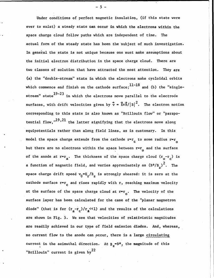
Under conditions of perfect magnetic insulation, (if this state were
ever to exist) a steady state can occur in which the electrons within the
space charge cloud follow paths which are independent of time. The
actual form of the steady state has been the subject of much investigation.
In geneial the state is not unique because one must make assumptions about
the initial electron distribution in the space charge cloud. There are
two classes of solution that have attracted the most attention. They are
(a) the "double-stream" state in which the electrons make cycloidal orbits
which commence and finish on the cathode surface;11-18 and (b) the "single-
stream" state1 9-2 3 in which the electrons move parallel to the electrode
surfaces, with drift velocities given by v = ExB/JBJ . The electron motion
corresponding to this state is also known as "Brillouin flow" or "parapo-
1119 ,21tential flow, the latter signifying that the electrons move along
equipotentials rather than along field lines, as is customary. In this
model the space charge extends from the cathode r=rc to some radius r=r
but there are no electrons within the space between r=r and the surface
of the anode at r=ra. The thickness of the space charge cloud (r -r c) is
a function of magnetic field, and varies approximately as (B*/Bz) . The
space charge drift speed vO=Er/Bz is strongly sheared: it is zero at the
cathode surface r=rc and rises rapidly with r, reaching maximum velocity
at the surface of the space charge cloud at r=r . The velocity of the
surface layer has been calculated for the case of the "planar magnetron
diode" (that is for (r a-r C)/r a<<l) and the results of the calculations
are shown in Fig. 5. We see that velocities of relativistic magnitudes
are readily achieved in our type of field emission diodes. And, whereas,
no current flow to the anode can occur, there is a large circulating
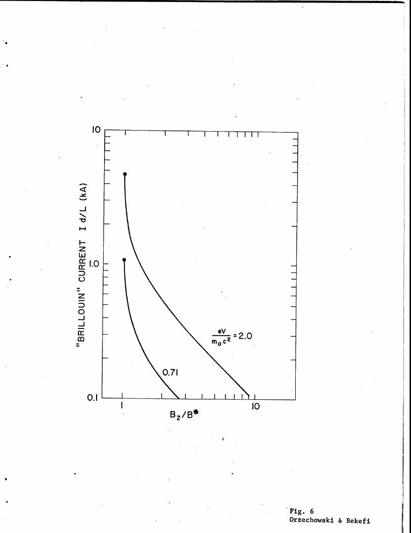
current in the azimuthal direction. At B - B*, the magnitude of this
22"Brillouin" current is given by
Page 7
- 6 -
I = (m c/ed)(L/y )(Yo-l)cosh (Yo) Amp. (3)
2where y 1 : + (eV/m c ) and L is the length of the cathode as measured
along the z axis. As Bz increases, I falls because the space charge
cloud becomes thinner. This variation with Bz is shown plotted in Fig.
6.
The opinion is that Brillouin flow is the more likely state into
which the system will settle initially provided that the risetime of the
voltage pulse is slow compared with the cyclotron period, so that adia-
baticity can be invoked in the equations of motion. This view is rein-
forced by computer calculations24 of the electron trajectories showing
the unmistakable evolution of the Brillouin state. Furthermore, it was
proved,25 for nonrelativistic cylindrical diodes at least, that the
Brillouin single stream state is the only one possible whenever r /ro C
< R=2 where r is the radius of the cathode and r is the radius of thec o
outer boundary of the space charge cloud. The parameter R is approxi-
mately equal to 2, but its magnitude varies somewhat with the value of
the current associated with the Brillouin ExB flow. The above inequality
is well satisfied in all our experiments where l<R<1.2.
It is generally accepted that a manifestation of currest flow across
the vacuum gap is due to a breakdown of the steady state assumption; namely,
time varying, organized, electric and magnetic field oscillations (i.e. in-
stabilities) develop resulting in the destruction of the steady state flow
and creation of large amplitude electromagnetic oscillations. And, it is
these oscillations that are the subject matter of section 3 below. It is
worth noting that the degree of organization of the oscillatory fields is
greatly enhanced by piercing the anode with a chain of coupled cavity res-
onators, a procedure one adopts in the practical magnetron devices. This
will be the subject of a subsequent paper (II) (see also ref. 26) where we
I
Page 8
- 7 -
shall show that, using our relativistic electron, field-emission cathode,
microwave oscillations in the gigawatt range of powers can be achieved.
2. THE EXPERIMENTAL ARRANGEMENT
The outer stainless steel anode is a cylinder 4.4 cm in diameter and
It is polished and has rounded edges to minimize local
field enhgncement and arcing.
dense, fine-grained graphite.
ing between 3.36 cm to 3.98 cm
with spacings d ranging from 2
via a stainless steel shank to
coaxial capacitor which serves
NEREUS high voltage facility.
rent viewing probe (see above)
The inner coaxial cathodeis machined from
A number of cathodes with diameters vary-
is used, thus providing diodes having gaps
.3 mm to 5.4 mm. The cathode is connected
the inner conductor of the water filled
as the transmission line of the 4 ohm
The anode is connected via a shielded cur-
to the outer, grounded wall of the capaci-
tor. The system is continuously pumped by means' of a diffusion pump to
pressures of approximately 5x10⁻⁵ Torr.
The axial magnetic field B acting on the diode is generated in a
solenoid energized by a capacitor bank whose rise time is approximately
6 msec. The discharging of this bank is timed in such a way that B
reaches its peak value when NEREUS fires. Thus, the magnetic field is
virtually constant in time over the duration of the 30 nsec voltage pulse
applied across the diode. The thin-walled, stainless steel construction
of the diode ensures good penetration of the pulsed magnetic field into
the diode interior. A magnetic field as high as 16 kG can be generated.
The diode current is measured with a rapidly resqonding, low-induc-
tance current viewing probe; its output is displayed on a fast oscillo-
scope. The diode voltage is obtained from the signa.L delivered by a
calibrated copper-sulphate voltage divider network and is corrected for
inductance effects.4,5
4.0 cm long.4 ,5
Page 9
- 8 -
The magnetron oscillations are diagnosed by monitoring the micro-
wave radiation emitted by the diode in an arrangement illustrated sche-
matically in Fig. 7. The waves emanate from the diode via a low loss
polystyrene window and are received by a microwave horn. The received
power is first attenuated to suitable levels by means of a precision at-
tenuator and then measured with a calibrated crystal detector connected
to a fastoscilloscope. Thus, the power P r(R,0,0) received at a given
point in space distant R from the diode, and at an angular position
(6,0) with respect to the diode axis is found with good accuracy. The
distance -R is sufficiently large so as to ensuie that the transmitting
magnetron diode and the receiving horn are in each others radiation
fields; that is R>2D 2A where D is the characteristic size of the trans-
mitter or receiver, whichever is the larger, and A is the wavelength.
With this choice of R, the power P emitted by the magnetron diode is re-
lated to the power received Pr, through the well -known radar formula2 7
eP r[16 2R R2 /GGr A2 (4)
where Ge is the gain of the transmitting diode and Cr the gain of the re-
ceiving horn. The receiving antenna is a standard horn and its gain Gr
is known. The gain of the emitter Ge is obtained by making an angular
scan of the transmitted power, and then deriving C from the relation-
ship2 7
4wP (0,4)
r-e fp (6,4)sinO d~d4)
Using the measured values of Pr (6,0), allows one to carry out numerically
the integration demanded in the denominator of Eq. (5).
From the foregoing procedure, the power emitted by the magnetron
diode is determined. The measurements are made over frequencies ranging
from 7 to 40 GHz with suitable microwave plumbing used for each of the
Page 10
- 9 -
four frequency bands needed to explore this large range: X-band (7-12.4
GHz), Ku band (12.4-18 GHz), K band (18-26.5 GHz) and Ka band (26.5-40
GHz). No measurements were attempted at lower frequencies because the
outer cylindrical anode acts as a waveguide beyond cutoff. It cuts off
the lowest TE1 1 mode at 4 GHz and the TE0 1 mode of interest here (see
below) at 8.3 GHz. The X-band receiver cuts off at 7.2 GHz.
The spectral distribution of the emitted radiation is determined by
interposing a length k of dispersive line between the receiving horn and
the crystal detector. The time delay t suffered by the signal relative
to the time (t=0) of the arrival of undispersed signal (see Fig. 7) al-
lows one to decompose the measurements into the various frequency com-
ponents, using the relationship that k = v -(w)t, where v (w) is the groupg g
velocity. The group velocity is obtained fron knowledge of the disper-
sion characteristics of the waveguide used in our experiments with the
result that the frequency w of the dispersed signal is given in terms of
the waveguide cutoff frequency wc by
O c[1 - (£/ct)2 -1/2 (6)
We use 155 meters of waveguide. Since only X-band waveguide of such
lengths is available to us, all our spectral frequency measurements are
made in the regime from -7 to -12 GHz.
3. MEASUREMENTS
The measurements fall into three categories. A study of the rf emis-
sion as a function of the externally applied magnetic field BZ; determin-
ation of the frequency characteristics; and a determination of the rf
electric field configuration, namely its polarization. We begin with a
discussion of the magnetic field dependence.
Page 11
- 10 -
(a) Magnetic Field Characteristics of the Emitted Radiation
In our experiments we adopt the following procedure. We arrange
the microwave instrumentation for the desired band (X, K, K, Ka)' We
set the externally applied magnetic field B -to a given value and charge
NEREUS to a fixed constant voltage. We then measure the total microwave
power Pr received by a small horn placed in the radiation zone of the
transmitting diode (Fig. 7), together with the diode current I and the
diode voltage V. With the same charging voltage we change the magnetic
field to a new value and repeat the measurements of P r, I and V. Note
that although the charging voltage is maintained the same throughout a
run, the voltage V across the magnetron diode varies somewhat with
changing Bz (see Fig. 4) because of changes in the diode impedance.
A series of successive shots like those described are then assembled
to yield Pr as a function magnetic field, at roughly constant diode volt-
age. The measurements are then repeated for all the remaining microwave
bands.
By scanning the magnetic field from B Z 0 to B = 16 kG we verifyz z
that within the sensitivity of our microwave detection system, no signi-
ficant radiation-occurs at any frequency until the magnetic field is
close to, or exceeds, the critical field B*. A further increase in the mag-
netic field causes the emission to rise sharply, reach a peak value at
some value Bz z (max), and then fall rapidly. This "resonant" behavior
is illustrated in Fig. 8 which shows plots of the radiation intensity in
two different frequency bands (X and K ) as a function of B . Measure-a z
ments made in other frequency bands show similar characteristics. These
can be summarized as follows. First, the radiation sets in at a certain
value of B near B - B* and the onset is the same at all frequencies.z z
Secondly, the peak in the microwave radiation occurs at a definite value
Page 12
- 11 -
of the applied magnetic field B - B (max): the value of B (max) is dif-z z z
ferent depending on the frequency band under investigation, as is clearly
seen from Fig. 8. Thirdly, the total power outputs P (obtained frome
radiation pattern measurements and use of Eqs. 4 and 5) are approximately
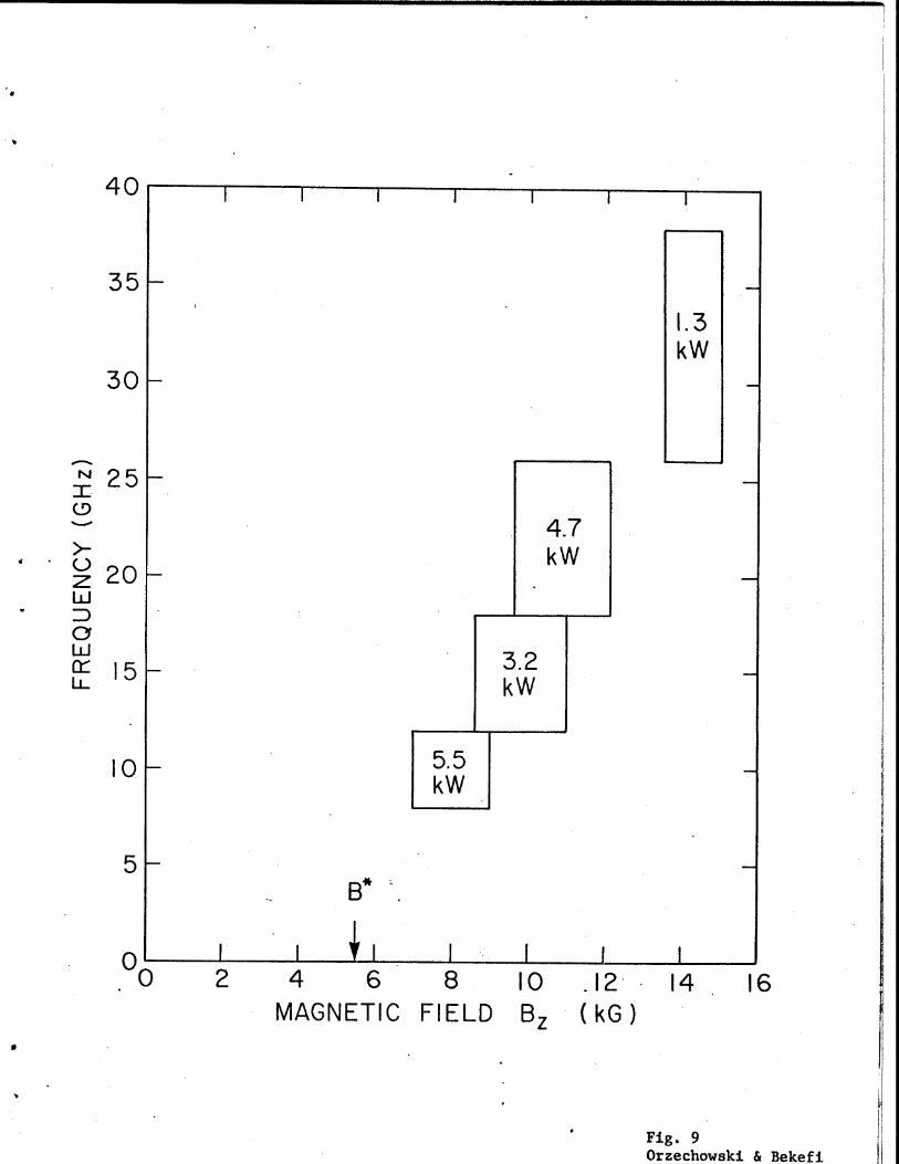
the same in all four frequency bands examined. Figure 9 illustrates both
the power and the tuning characteristics of the diode. In each of the
four microwave bands the total emitted power is typically 1 to 5 kW. And,
the higher the externally applied magnetic field, the higher is the fre-
quency of the microwaves received. The "tuning" relationship is approxi-
mately linear and is of the form
f = 3.4xlO 9(B z-B*) Hz (7)
where B is in kG.
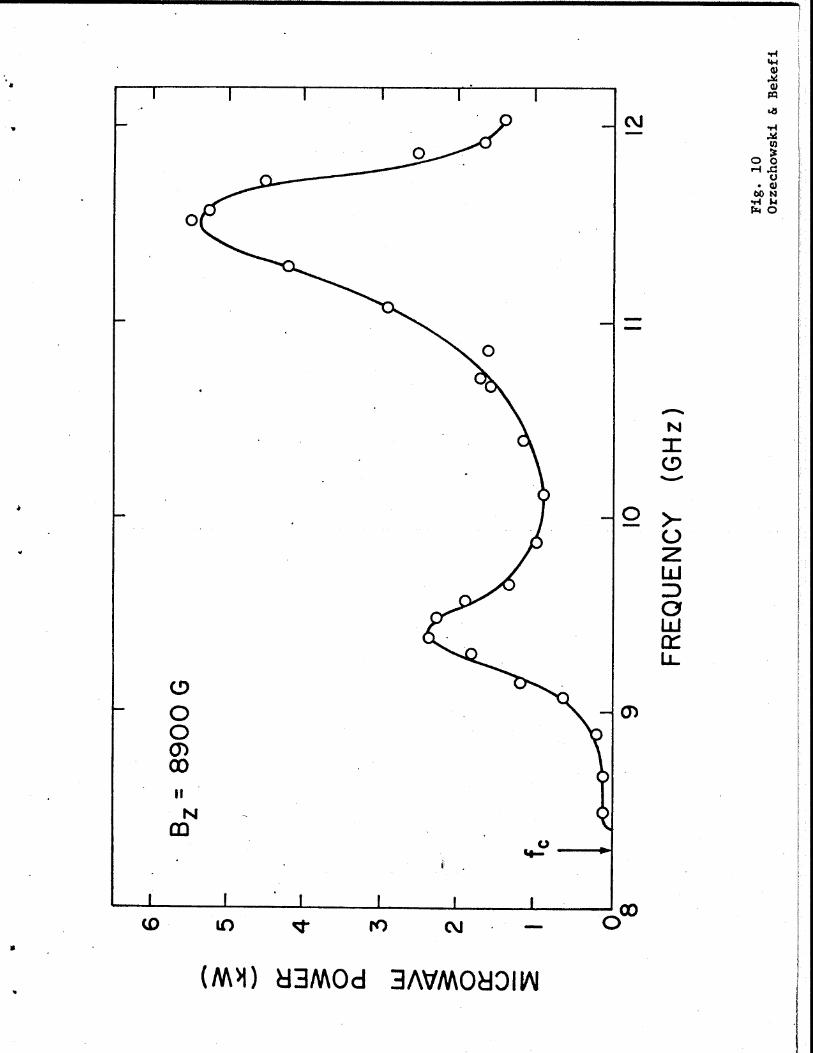
(b) Frequency Characteristics
The shape of the curves shown in Fig. 8 and the tuning characteris-
tics illustrated in Fig. 9 point to the fact that we are dealing here with
multiple resonance behavior. Spectral measurements in which we observe
one, two, and even several resonances bear this out. The measurements are
carried out (for fixed Bz and diode voltage V) by means of the dispersive
line described in Section 2. Figure 10 is typical of such observations.
It shows that at a given magnetic field (which.we have chosen in the
figure to be that corresponding to maximum emission at X-band) there are
two fairly wide (<l GHz) resonances. As the magnetic field is varied,
the frequency positions of the resonances and their separation remain un-
changed even when the magnetic field is varied by as mch as a factor of
two. However, their amplitudes vary strongly with Bz and reach maximum
values only for a certain fixed B =B z(max). New resonances may appear at
widely different magnetic fields but usually there is only one very strong
resonance flanked by one or more rather weak ones.
Page 13
- 12 -
Are the above resonances inherent to the emission process of the
radiating electrons such as cyclotron or plasma oscillations, and are
they therefore governed by the dispersion characteristics of the electron
gas? The answer is no. The resonances are system resonances that are
there even in the absence of the electrons. This has been verified in
"cold tests" of the diode. A low level microwave signal of variable
frequency, is injected into the diode and a small probing antenna measures
the response. One then finds resonances having identical frequencies
and Q's as in the operating diode. A second test is used to verify that
the resonances are simply system resonances of what is after all a
fairly complicated cylindrical resonant cavity. We vary the gap width d
and find no change in the emission spectrum, despite the fact that the
Brillouin space charge flow is a sensitive function of d.
Thus, the following picture emerges concerning the spectral character-
istics of the radiation. Copious emission, exceeding expected thermal
levels by many orders in magnitude, is generated by the rotating electron
space charge cloud. The cloud is unstable resulting in the production of
intense rf electric field fluctuations which exist over a fairly broad
frequency spectrum. As a result of system resonances, the electromagnet-
ic radiation ultimately emanating from the diode is enhanced at those
particular frequencies which correspond to certain resonant frequencies
of the "cold" resonator system. In other words, the emission "locks onto"
one or another of the many possible cavity modes. The resonances can be
tuned with magnetic field and are observed in one of two ways: from the
frequency spectrum, at constant Bz (Fig. 10); or by sweeping B , keeping
the observation frequency fixed constant over the discrete frequency bands,
X, Kua, K, K (Figs. 8 and 9).
Page 14
- 13 -
(c) Polarization
The radiation emanating from the polystyrene window is strongly
polarized, with electric field lines forming predominantly concentric
circles about the diode axis. This is verified by placing two receiving
horns in the radiation zone at fixed and equal distances R from the diode
and scanning in angles e or *. The horns are rotated at right angles to
one another and are thus sensitive to orthogonal electric field polariza-
tions. In addition to the strongly polarized field, there is evidence of
a weak background of randomly polarized radiation.
The strongly polarized component is consistent with the emission from
a circular waveguide excited in the TE01 mode (or possibly in a higher
TE mode). The accompanying radiation pattern obtained by sweeping the
angle 0 at constant R and $ is illustrated in Fig. 11 for Ka band frequen-
cies. The "butterfly shaped" pattern with two well-pronounced wings, and
a minimum in intensity at 0=$=0 is typical28 of'the TE01 mode of excita-
tion. (The same type of radiation pattern is also seen at X, Ku, and K
band frequencies.) As additional verification, we point out that no emis-
sion from the diode is ever observed at a frequency below approximately
8.2GHz (see Fig. 10). Nowthe cutoff frequency of a cyclindrical wave-
guide oscillating in the TE01 mode is given by fc = 0.610(c/a) where a
is the radius. With a = 2.22cm, fc = 8.3 Giz, a result which is in good
agreement with observations. We note in passing that the TE mode is
not the lowest (or fundamental) mode of a circular pipe. The lowest mode
is the TE1 1 mode which has a cutoff frequency (for our radius of pipe)
equal to 4.0 GHz.
4. DISCUSSION
The intensity of the rf electric field fluctuations associated with
Page 15
- 14 -
observed microwave power output must, indeed, be quite substantial. Take
a power output of 5kW and assume a 10 percent efficiency of converting
electromagnetic energy within the 3.4mm cathode-anode gap into transverse
electromagnetic wave energy outside the diode. It then follows from
Poynting's flux that the- peak electric fields in the gap are typically
9 kV/cm, or approximately equal to 1 percent of the dc radial electric
field applied across the anode-cathode gap. This agrees with earlier
estimates made for conventional magnetrons in which fluctuations as high
as 10 percent of the dc value have been reported.2 9
That fluctua:ions set in at the critical magnetic field BZ=B* points
to the fact that the instability is associated with the Brillouin space
charge flow which sets in precisely at this critical field. As noted in
Section 1, the azimuthal flow is sheared which can result in the so-called
slipping stream30 or diochotron instability. It is a space charge insta-
bility in which the surface of the Brillouin cloud becomes rippled in the
azimuth; associated with this rippling is an azimuthal rf electric field.
This field has the correct polarization to excite a TE mode in the
circular diode. The fact that the observed emission is principally in
the TE01 mode lends credence to our belief that we are in fact dealing
here with a manifestation of the slipping stream instability. In parti-
cular, we think that it is a slipping stream mode effected by resistive
wall effects.30 The latter makes the instability "go" at frequencies less
than the cyclotron frequency, as observed by us. To verify this, however,
would require a measurement of the wavelength of the instability and com-
parison with the theoretically predicted dispersion equation. Unfortu-
nately, the measurement of the wavelength of the space charge fluctuations
is difficult if not impossible in our pulsed d-iode.
Other instabilities come to mind, particularly those at frequencies
Page 16
- 15 -
corresponding to the electron-cyclotron and electron-plasma frequencies.
The first can be ruled out on the grounds that all our measurements show
(Fig. 9) that the emission is broad band and occurs well-below the rela-
tivistic cyclotron frequency wc = eB/my. The second is ruled out for the
same reason, since for space charge limited flow, the plasma frequency wp
equals the cyclotron frequency wc.
The presence of ions (due to anode and/or cathode plasma formation)
can lead to ion type of instabilities which have sometimes been seen 31in
conventional magnetrons. However, these instabilities result in low fre-
quency fluctuations in the range of tens of megahertz. If they are pres-
ent in our diode, they could not be observed by our measureing technique.
In conclusion, then, we have shown that a strong correlation exists
between the observed anomalous current flow across the relativistic mag-
netron diode when B z>B*, and the intense microwave emission emanating
from it. We believe that the origin of the emission is a form of the
slipping instability in the Brillouin space charge flow. A full electro-
magnetic and relativistic r,0 particle simulation code is under develop-
32ment with whose aid we hope to be able to answer this question. In
particular, we expect that the code will yield information about the de-
pendence of the diode current on magnetic field (see Fig. 4), a problem
that has so far defied detailed theoretical understanding (but see
Mouthaan and Siisskind of Ref. 30).- Needless to say, the smooth-bore mag-
netron has little or no application as a device forgnerating microwaves.
It has poor efficiency, and the emission spectrum is broad and not readily
controlled. But, it is, so to speak, the basic building block of real
magnetron devices which differ from the smooth-bore in that the anode
block is pierced by a series of coupled resonators. The oscillations
seen in the smooth-bore diode are believed to come close to the startup
Page 17
- 16 -
conditions of the real device. Thus, in the initial state (often referred
to as the "preoscillation stage") the interaction is predominantly quasi-
electrostatic in character: the electrons interact collectively with longi-
tudinal space charge electric fields generated in the bulk and near the
surface of the space charge cloud. The associated Poynting flux is rela-
tively small. This differs from the fully developed oscillating stage of
the magnetron device which is characterized by strong energy exchange be-
tween the electrons and the transverse electromagnetic fields which exist
outside the main space-charge cloud, that is, between the anode and the
space charge bouindary. The strong interaction is the consequence of elec-
tromagnetic modes that are in phase synchronism with the rotating Brillouin
cloud. Now the Poynting flux becomes enormous, but this is the subject
matter of a subsequent report (paper II).
Page 18
- 17 -
REFERENCES
1. J. A. Bradshaw, article in "Crossed-Field Microwave Devices", E.
Okress, editor (Academic Press 1961) Vol. 1, p. 261, plus references
in this article.
2. J. M. Osepchuk, article in "Crossed-Field Microwave Devices", E.
Okress, editor (Academic Press 1961) Vol. 1, p. 275, plus references
in this article.
3. G. D. Sims, article in "Crossed-Field Microwave Devices", E. Okress,
editor (Academic Press 1961) Vol. 1, p. 179.
4. T. J. Orzechowski and G. Bekefi, Phys. Fluids 43, 19, (1976).
5. G. Bekefi, T. J. Orzechowski, and K. D. Bergeron, First International
Topical Conference on Electron Beam Research and Technology, Albuquer-
que, 1975, National Technical Information Service, U.S. Department of
Commerce Vol. I, p. 303, 1976.
6. 0. Buneman, Nature 165, 474 (1950).
7. A. W. Hull, Phys. Rev. 18, 31 (1921).
8. L. Page, Phys. Rev. 18, 58 (1921).
9. R. V. Lovelace and E. Ott, Phys. Fluids 17, 1263 (1974).
10. L. Tonks, Phys. Sowjetunion 8, 572 (1936); K. D. Bergeron and J. W.
Poukey, Appl. Phys. Letters 27, 58 (1975).
11. D. R. Hartree, C.V.D. Rept. Mag. 1 (1941).
12. J. Slater, "Microwave Electronics", Van Nostrand 1950.
13. J. L. Delcroix, Thesis, Paris University 1953 (unpublished).
14. D. Gabor, Proc. Roy. Soc. A,183, 436 (1945),; i.. Gabor and G. D. Sims,
J. Electronics 1, 25 (1955).
15. R. Q. Twiss, Advances in Electronics 5, 247, (05>3); J. Electronics
1, 1 (1955).
Page 19
-18 -
16. R. N. Sudan and R. V. Lovelace, Phys. Rev. Letters 31, 1174 (1973).
17. R. V. Lovelace and E. Ott, Phys. Fluids 17, 1263 (1974).
18. A. Ron, A. A. Mondelli, and N. Rostoker, IEEE Trans. Plasma Sci.
PS-1, 85 (1973).
19. L. Brillouin, Phys. Rev. 60, 385 (1941); 62, 166 (1942); 63, 127
(1943); L. Brillouin, and F. Block, Advances in Electronics 3, 85
(1951); 3, 145 (1951).
20. 0. Buneman, Nature 165, 474 (1950); J. Electronics and Control 3,
1 (1957); 3, 507 (1957); C.V.D. Rept. Mag. 10, 11, 17, 30. (1943).
21. B. C. DePackh, Naval Research Laboratory Radiation Project Progress
Report No. 5 (1968); 17 (1969). (Unpublished).
22. E. Ott and R. V. Lovelace, Appl. Phys. Letters 27, 378 (1975).
23. J. M. Creedon, J. Appl. Phys. 46, 2946 (1975); 48, 1070 (1977); S. A.
Goldstein, R. C. Davidson, J. G. Siambis and R. Lee, Phys. Rev.
Letters, 33, 1471 (1974).
24. 0. Buneman, article in "Crossed-Field Microwave. Devices", E. Okress,
editor (Academic Press, 1961) Vol. 1 p. 209.
25. W. P. Allis, M.I.T. Radiation Laboratory Report No. V-9,S, Oct. 1941.
26. G. Bekefi and T. J. Orzechowski, Phys. Rev. Letters, 37, 379 (1976).
27. S. Silver, "Microwave Antenna Theory and Design", M.I.T. Radiation
Laboratory Series Vol. 12 (McGraw-Hill, 1949) p. 4.
28. N. Marcuvitz, "Waveguide Handbook", M.I.T. Radiation Laboratory Series
Vol. 10 (Boston Technical Publishers, Inc., 1964) p. 201.
29. C. W. Hartman, Electronics Research Laboratory Report No. 10, 1960,
University of California, Berkeley, California.
30. 0. Buneman, article in "Crossed-Field Microwave Devices", E. Okress
Page 20
- 19 -
editor (Academic Press 1961) Vol. 1, p. 367; C. G. Macfarlane and
-H. G. Hay, Proc. Phys. Soc. 63, 409 (1950); K. Mouthaan and C.
Susskind, J. Appl. Phys. 37, 2598 (1966); 0. Buneman, R. H. Levy
and L. M. Linson, J. Appl. Phys. 37, 3203 (1966).
31. V. I. Farenik, V. V. Vlasov, A. M. Rozhkov, K. N. Stepanov, and V. A.
Suprunenko, Zh. Tekh. Fiz. 42, 1625 (1972) [Sov. Phys. Tech. Phys.
, 1298 (1973)]; also Zh. Eksp. Teor. Fiz Pis. Red. 10, 71 (1969)
[J.E.T.P. Lett. 10, 46 (1969)].
32. An early attempt at this was madeby S. P. Yu, G. P. Kooyers and 0.
Buneman, J. Appl. Phys. 36, 2550 (1965).
I
Page 21
- 20 -
FIGURE CAPTIONS
Fig.- 1. Geometry of the smooth-bore magnetron.
Fig. 2. Diode perveance as a function of the normalized magnetic field
B /B*, for different gap widths d. The perveance is determinedz
at a time during the 30 nsec pulse when maximum current is
drawn to the anode. The curves for the different gap widths
are displaced vertically with respect to one another by a fixed
interval, for easier visual presentation. Absolute magnitudes
of the perveance, at Bz=0, for each of the four gaps, are re-
spectively: 1052 (1149); 589 (522); 329 (310); 202 (205) PAV-3/2
where the values in parentheses are from the Child-Langmuir
theory.
Fig. 3. Normalized electron current I/IL as a function of the normalized
magnetic field Bz /1*. CL is the Child-Langmuir current in
the limit, B +0. The "hot tial" at B >B* has been omitted fromz z
this figure for the sake of clarity. The various points are ex-
perimental values obtained for different gap widths: 0 0, d
2.3 mm; S 0, d = 3.4 mm; X X, d = 4.4 mm; A A, d = 5.4 mm.
The solid line is from theory5,10 for a planar diode in a
uniform magnetic field. The dashed curve is from Eq. (2).
Fig. 4. Diode current and diode voltage as a function of magnetic field,
for a gap width d = 3.4 mm. The current (and voltage) are mea-
sured at a time during the pulse corresponding to maximum current
flow. The critical magnetic field B* - 5.5 kG.
Fig. 5. Brillouin drift velocity of the outermost space charge layer of
a planar diode, as a function of magneitc field, calculated for
different diode voltages V.
Page 22
- 21 -
Fig. 6. The azimuthal Brillouin current calculated in the limit
(r a-r c)/r a<<1 of a plasma magentron diode, as a function of
magnetic field. The value of current at B =B* shown by thez
heavy dot is given by Eq. 3. Only part of this current appears
across the diode when magnetic insulation breaks down, but pre-
cisely what fraction depends on the spectrum and amplitude of
the turbulent rf fields, and is a largely unsolved problem (but
see Mouthaan and SUsskind of Ref. 30).
Fig. 7. Experimental arrangement used in studying microwave emission
from the diode.
Fig. 8. Total microwave power emitted in two frequency bands, as a
function of magnetic field; d = 3.4mm.
Fig. 9. Frequency and power of emitted radiation as a function of mag-
netic field. In each frequency band the magnetic field
BZ = B Z(max) is adjusted to give maximum power output (see Fig. 8).
Fig. 10. Spectrum of emitted radiation in the X-band range of frequencies;
f is the cutoff frequency of the TE01 mode.
Fig. 11. Observed radiation pattern (i.e. a polar plot of intensity as a
function of angle e) in the Ka band range of frequencies (26-40
GHz). The fact that the intensity does not go exactly to zero
on axis (0=90*) is partly due to the finite size of the receiving
horn and partly due to the presence of a weak component of ran-
domly polarized radiation.
Page 23
. . . . . ....
. .. . . . . .
.............
. . ~~ .*** ..........
.~~~ ......
.. ....... .:*
.... .....
.. . . .. . . ....~.
.......... V.:............. .....
. .. .............. * * ..
. .. ........ . *****~. :.
.. . .. . ... .
. . . . . . . . . .....
.......... B kef
Page 24
d =0.23cm
d =0.34cm0~o
i
d =0.44cm**L 7 k-------------------------
L .
d =0.54cm
z
Lii
Li[ x
0- 3 10-2 10'1 10
NORMALIZED MAGNETIC FIELD B /B*Fig. 2Orzechowski & Bekefi
Page 25
1.0
''N
0.8
Nez V*
> 0.6 x-x
~0.x- LL *x \X0.4
< o
Z0.2
00 0.2 0.4 0.6 0.8 1.0
NORMALIZED MAGNETIC FIELD Bz/B
Fig. 3Orzechowski & Bekefi
Page 26
00tO)
00N
00
"14
0
*Gi
0I I I I I I I I
w0
0
00
0
0
0
-J
0(0 O 0
LO 114
00
00Lu6
*6
0 0r( N
0 0
.iN388no
00'I-
*1.4tI.40)
0)
0C'j
(-9
(0Nm
0-J.
Cj LL
CC
0
Udz0
0
30010
(AN) 3"E"Vi-10A
(V'>) I
Page 27
1.0
0>-
--
0.9
0.8
0.7
0.6
0.5
0.4x
0.3
Li 0.2
0.1
0
CURVE eV/ m c2
- --- 0.51----- 0.71
-...------------ .- 1.0
2.0
-- I
I-
I CUVE e/m~c
0 2 3 4 5 6NORMALIZED MAGNETIC FIELD Bz /B*
Fig. 5Orzechowski & Bekefi
7I I I I I II
Page 28
10 r- - --7
-zw
0..0
00
z
0
evm m~c2 2.0
0.71
0.1I
B,/B* J
Fig. 6Orzechowski & Bekefi
Page 29
144
L'4-
Lij z
uci
ILl-FU) r
00
LLI UU
(C U)0
>U):>-Z
> 000 F-
U) -LIJ 3:
cr-U) Diu
a- rZ 0
zu~ z
a_ 0
LLu
F-r
LIJu
00
U)
Page 30
I I I I I I I I I I
41-
3
3:
0
2
f = 8-12GHz
0 f = 27-0
000
0
0 0
I
8 12AXIAL MAGNETIC FIELD
16Bz (kG)
20
Fig. 8Orzechowski & Bekefi
Lu
0
C)
40 GHz
I
4,
Page 31
I I
3.2kW
5.5kW
I 41I4 6
MAGNETIC8
FIELD10
Bz
Fig. 9Orzechowski & Bekefi
40
35K
301-
1.3kW
25F
20KzwZD
LL-
4.7kW
15
10
5H
01C 2 .12,
(kG)14 16
I I
I I I i I
I I I
Page 32
-H.
0 0
u
Nt4 0-
C
CCa
)O
--
N
N
zD
UL-
4-. -~
w"V.'
0
(MNi) 83MOd 3AVMOHWDIY
440
N~
0
0)
II
a
(0 Uf) re) N~I I
I I I I I
II
Page 33
a 0
00 000 T-40
too0 4C\j
C\J
d00
00
00
00
(00
0 ~ 00