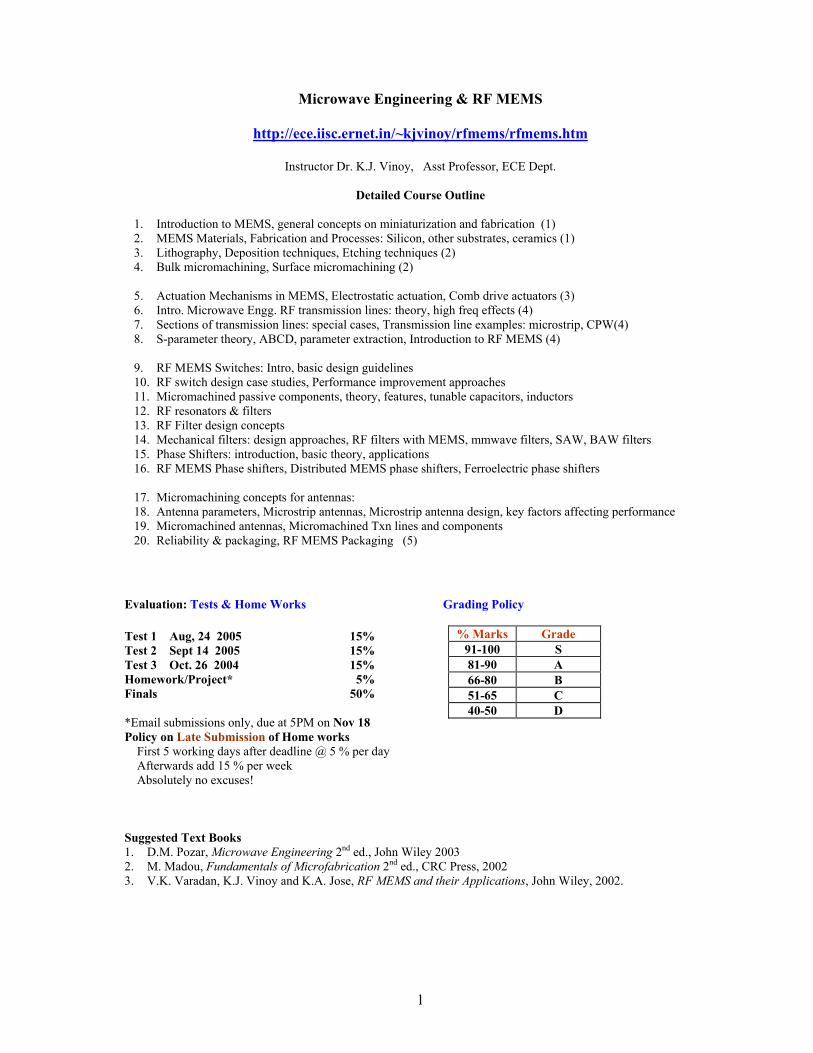
Test 1 Aug, 24 2005 15% Test 2 Sept 14 2005 15% Test 3 Oct. 26 2004 15% Homework/Project* 5% Finals 50% *Email submissions only, due at 5PM on Nov 18 Policy on Late Submission of Home works First 5 working days after deadline @ 5 % per day Afterwards add 15 % per week Absolutely no excuses!
Grading Policy
% Marks Grade 91-100 S 81-90 A 66-80 B 51-65 C 40-50 D
Suggested Text Books 1. D.M. Pozar, Microwave Engineering 2nd ed., John Wiley 2003 2. M. Madou, Fundamentals of Microfabrication 2nd ed., CRC Press, 2002 3. V.K. Varadan, K.J. Vinoy and K.A. Jose, RF MEMS and their Applications, John Wiley, 2002.
2
Other Reference Books Microwave Engineering 4. I Bahl, Lumped Elements for RF and Microwave Circuits, Artech House 5. R.E. Collin, Foundations for Microwave Engineering, IEEE Press 6. R. Mongia, I.J. Bahl, and P. Bhartia, RF and Microwave Coupled-Line Circuits, Artech House, 1999. 7. I. Bahl & P. Bartia, Microwave Solid State Circuit Design, Wiley Inter Science, 2003. Microfabrication & MEMS 8. S. Senturia, Microsystem Design, Kluwer, 2001. 9. J.W. Gardner , V.K. Varadan , O.O. Awadelkarim, Microsensors, MEMS & Smart Devices John Wiley, 2001. 10. S. Campbell, The Science and Engineering of Microelectronic Fabrication, Oxford Univ. Press, 2001 11. N Maluf An Introduction to Microelectromechanical Systems Engineering, Artech House 12. M Elwenspoek R. Wiegerink, Mechanical Microsensensors, Springer 2001 13. G.T. Kovacs, Micromachined Transducers Sourcebook, McGraw Hill Science, 1998 14. M. Gad El Hak The MEMS Handbook, CRC Press 2001. RF MEMS 15. G. Rebeiz, RF MEMS: Theory, Design, and Technology, Wiley/IEEE Press, 2003 16. H.J. De Los Santos, Introduction to Microelectromechanical (MEM) Microwave Systems, Artech house, 1999. 17. H.J. De Los Santos, RF MEMS Circuit Design for Wireless Communications, Artech House, 2003 Journals of Interest IEEE/ASME J. Microelectromechanical Systems IEEE Trans. Microwave Theory & Techniques J. Micromechanics and Micromachining (IOP) IEEE Microwave & Wireless Components Letters Websites of Interest 18. http://www.nexus-mems.com/ E uropean microsys net 19. http://guernsey.et.tudelft.nl/indexold.html - Silicon Microoptics in Delft 20. http://guernsey.et.tudelft.nl/farlinks.html 21. http://www.dimes.tudelft.nl/ DIMES delft institute of microelectronics and
MEMS clearinghouse 25. http://transducers.stanford.edu/ Stanford transducers lab 26. http://www-bsac.eecs.berkeley.edu/ Berkeley Sensor & Actuator centre 27. http://mems.jpl.nasa.gov/home.html JPL-MEMS 28. http://www.analog.com/index.html look up MEMS technology at Analog devices 29. http://www.mcnc-rdi.org/index.cfm MCNC research home page 30. http://www.mems.louisville.edu UofL MicroTechnology Web Site 31. http://www.dbanks.demon.co.uk/ueng/ Introduction to Microengineering by Dr. Daniel Banks 32. http:/www.dbanks.demon.co.uk/ueng/ Microsystems, Microsensors & Microactuators by Dr.
Daniel Banks 33. http://www.ee.surrey.ac.uk/Personal/D.Banks/roughgui.html Introduction to Microengineering 34. http://www.memsrus.com/cronos/svcsmumps.html MUMPS Design Handbook 35. www.memsrus.com/cronos/mumps.pdf The course material will be from various resources listed above.
3
Electromagnetic spectrum of relevance
HF 3-30 MHz VHF 30-300 MHz UHF 300-1000 MHz RF L 1-2 GHz S 2-4 GHzٻ C 4-8 GHz Microwave X 8-12 GHz Ku 12-18 GHz K 18-27 GHz Ka 27-40 GHz V 40-75 GHz W 75-90 GHz mm wave 30-300 GHz
Wavelength & frequency
GHzcm ff
c 30][ =→= λλ
History/ Evolution/ Trends in RF Engineering
Popular application Frequency Early 20th century Radios ~ MHz mid- 20th century TV 100’s MHz late 20th century Mobile phones ~ 1 GHz early 21st century (Wireless systems) 2-5 GHz Bluetooth/ WLAN Next?? Future generation (?) 20-50 GHz (?)
Behavior RLC Components at High Frequencies All components (passive, active, and even interconnects) need to be viewed as distributed parameter networks. We will consider resistors, capacitors, inductors, and the skin effect in conductors. Recall some fundamental principles:
Resistance - occurs in any conducting medium (except superconductors) and limits the flow of current. Capacitance - occurs whenever two conductors are separated by a dielectric. Inductance - occurs whenever magnetic flux links a conductor.
The physical dimensions and material properties of the components determine the equivalent distributed parameter network and we model the component as a network of discrete components. Resistor
4
Capacitor
Inductor
Observe that
• All components have resistance, capacitance, and inductance. • At low frequencies, the unintended components are insignificant. • At high frequencies, these unintended components become significant. • The unintended components are distributed throughout the device. These devices should therefore be
modeled with a network of discrete devices. • As a rule of thumb, when the average size of a discrete component is more than a tenth of the wavelength,
the distributed parameter network model, i.e., transmission line theory, should be used. (Use the wavelength in the medium, not the free-space wavelength)
Some of the issues with Conventional RF/Microwave Circuits Issue Result Poor modeling Discontinuity effects Radiation leakage to, and/or out of the substrate Formation of multiple modes Poor Q-factor Excess bandwidth, reduced selectivity of filters, increasing input noise power Excess insertion loss, reduced output power, efficiency Excess localization of heat dissipation (requiring thermal management) Excess noise temperature, reducing sensitivity of receivers Poor line-to line isolation Low directivity, reducing efficiency of directional couplers High cross-talk, increasing stability problems in amplifiers and oscillators Increasing mutual coupling between antenna elements Stray coupling between standards, increasing measurement uncertainty.
Excess line lengths, further increasing insertion loss Low package density Excess chip sizes, increasing cost
5
This course addresses the possibility of Microfabricated components and their use in RF engineering What are RF MEMS?
• Components used for RF, Microwave and millimeter wave systems • Small devices, with feature size of micron order • Fabricated by micro- (and nano-) technologies • These are devices for RF applications, made by microfabrication route
• Micro-Switches/Micro-relays • Capacitors and Inductors • Resonators and Filters • Phase Shifters • Antennas, Planar transmission lines
6
7
Introduction to Microsystems Technology Definitions Microelectromechanical Systems (MEMS) Miniaturized device or an array of devices, combining electrical and mechanical components, fabricated using IC batch production techniques. Also called Microsystems, micromechanical systems, etc. MEMS is usually an integration of mechanical elements, sensors, actuators, and electronics on a common substrate (usually silicon) through microfabrication technology. While the electronics are fabricated using IC process sequences (e.g., CMOS (most common now), Bipolar, or BICMOS processes), the micromechanical components are fabricated using a set of "micromachining" processes that selectively etch away parts of the wafer or add new structural layers to form the mechanical and electromechanical devices. Actuator A device that generates force to manipulate itself, or another mechanical device, or the surrounding environment to perform some useful function Sensor A device that collects useful information from the surrounding environment, and provides one or more output variables to a measuring instrument Smart Sensor A sensor with built-in intelligence (usually integrated). This will have the necessary control and electronics built-in on-chip, or separately on another fabricated by IC technology, and packaged together. Substrate A material that supports (or forms part of) the device. (Usually silicon, ceramic, glass, or plastic) Note: if the substrate is semiconductor material such as Si, GaAs, the electronics may be built in. Another possibility: organic electronics) Structural Layer A layer of thin film material that comprises a mechanical device. The layer is fabricated on the sacrifical layer, and then released by etching it away. Sacrifical Layer A layer of material that is deposited between the structural layer and the substrate to provide mechanical separation and isolation between them. This is removed after the mechanical components on the structural layer are fully formed, by release etch. This approach facilitates the free movement of the structural layer with respect to the substrate. Minimum Feature Size The lateral dimension of the smallest feature on the structural layer Vertical Aspect Ratio Ratio of the height of the structural layer to the minimum feature size Die Footprint The total area on the substrate that the (entire) device occupies. MEMS Technology Milestones Credited to Physicist R. Feynmann “There’s plenty of room at the bottom” 1956 Bulk etching of Si wafers for pressure sensors 1970s Pioneering work: K. Peterson “Silicon as a structural material” (properties, etching data) 1982 Surface micromachined polysilicon, comb drive actuators, disc drive heads 1980’s Optical Applications MOEMS 1990’s RF/microwave applications RF MEMS 1990’s Major Areas of MEMS Applications (industry-wise) • Automobile/Transportation • Defense, Space • Medical/Biological • Industrial/Control • Telecom (RF & Optical)
8
MEMS Components for Automotive/Transportation Segment
Micromachine Application Present Availability Status Absolute pressure sensor Manifold absolute pressure (MAP) sensing Available Accelerometer Air-bag release Available Temperature sensors Inside and outside vehicle Available Level sensor Oil and gas level Available Light sensor Turn on the lights Available Solid state cameras Looking behind truck or car Available Pressure sensors e.g., for exhaust gas recirculation Available Rain sensors Automatic Available Parking sensors Collision avoidance Available Oxygen sensor Air/gas ratio Available, but needs better Air flow sensor Air/fuel ratio control Expensive, not micromachined Head-up display Information on window Not affordable yet Alcohol sensor Detection of alcohol level in blood of
drivers No reliable products available
Humidity sensor Cabin climate Unsatisfying products available
Tire pressure sensor Pressure reading on board Under development Torque sensors Work Under development Battery sensor charge/density Contraband detector
Customs Research
Azide sensor Air bag propellant Charge/density of electrolyte
Does not exist
Driver identification Theft prevention No good solutions Fuel flow sensor No good solutions yet Gyros Navigation No inexpensive solutions Spill detector Truck accidents clearing No good solutions available Micro-nozzle system Fuel injection NOX Sensor Pollution control Not available Oil quality monitor Engine protection Not available Roadlbridge condition sensors
Preventive road maintenance Not available
Road sensors Roughness, ice, rain Not available at cost Smart windows Defog, clear view Not available at low cost
Defense/Space Accelerometers Angular rate sensors/gyroscopes Micropropulsion systems Micropumps RF components for radar and communications IR imagers Medical/Bio
Drug delivery systems Patches Cygnus GlucoWatch Biographer External and implantable pumps Debiotech micropump, Smart pill ChipRx smart pill, Monitoring Point -of-care testing i-STAT's hand-held blood analyzer On-line monitoring of blood gases See RT-MECSS from microbioncs On-line monitoring of pressure Several disposable pressure sensors available (<$1)
9
Prostheses/artificial organs Orthopedics, ophthalmology Nanotexturing of surfaces for enhanced biocompatibility of implants Neurology MEMS neural stimulator probes Cardiology Pacemakers One- or two-axis accelerometers for activity monitoring Angioplasty catheters Several disposable pressure sensors available (<$1) Biotechnologies Polymerase chain reaction (PCR) PCR efforts, e.g., at Cepheid Genetic tests and therapy Nanogen's NanoChipTM Electrophoresis See Caliper and Acalara lab-on-a-chip (LaC) technologies Liquid handling systems See e.g., Micronics fluidic T-sensor technology Minimally invasive surgery Cutting tools Painless ultrasonic cutting tools at the University of Wisconsin
Industrial/Automation IR imagers Gyroscopes Accelerometers Valves Pressure sensors ISFETs (ion-senitive FET) Telecom/IT Optical switches Microrelays RF components Attenuators and equalizers Ink-jet print heads Memory device RW heads Projection displays Gyros Why Miniaturization? Some common features of miniaturization include: • Minimizing of energy and materials consumption during manufacturing • Redundancy and arrays • Integration with electronics, simplifying systems (e.g., single point vs. multipoint measurement) • Reduction of power budget • Taking advantage of scaling when scaling is working for us in the micro domain, e.g., faster devices, improved
thermal management, etc. • Increased selectivity and sensitivity • Minimally invasive • Wider dynamic range • Exploitation of new effects through the breakdown of continuum theory in the micro domain • Cost/performance advantages • Improved reproducibility • Improved accuracy and reliability • Self-assembly and biomimetics with nanochemistry • More intelligent materials with structures at the nanoscale
10
MEMS: Materials, Fabrication and Processes
Alloys
Materials for MEMS
Substrates Thin films Packaging
Plastics Glass
Ceramic Semiconductor
MgO Alumina
Sapphire
Si GaAs
InPGe
Al
Semiconductor
Metal
Poly-silicon
Special materials
Plastics
Ceramic
Metal
Au Cu
Pt
Ti Ag
Pd
Dielectrics
PZT STO BST
SiO2 Si3N4
PMMA
11
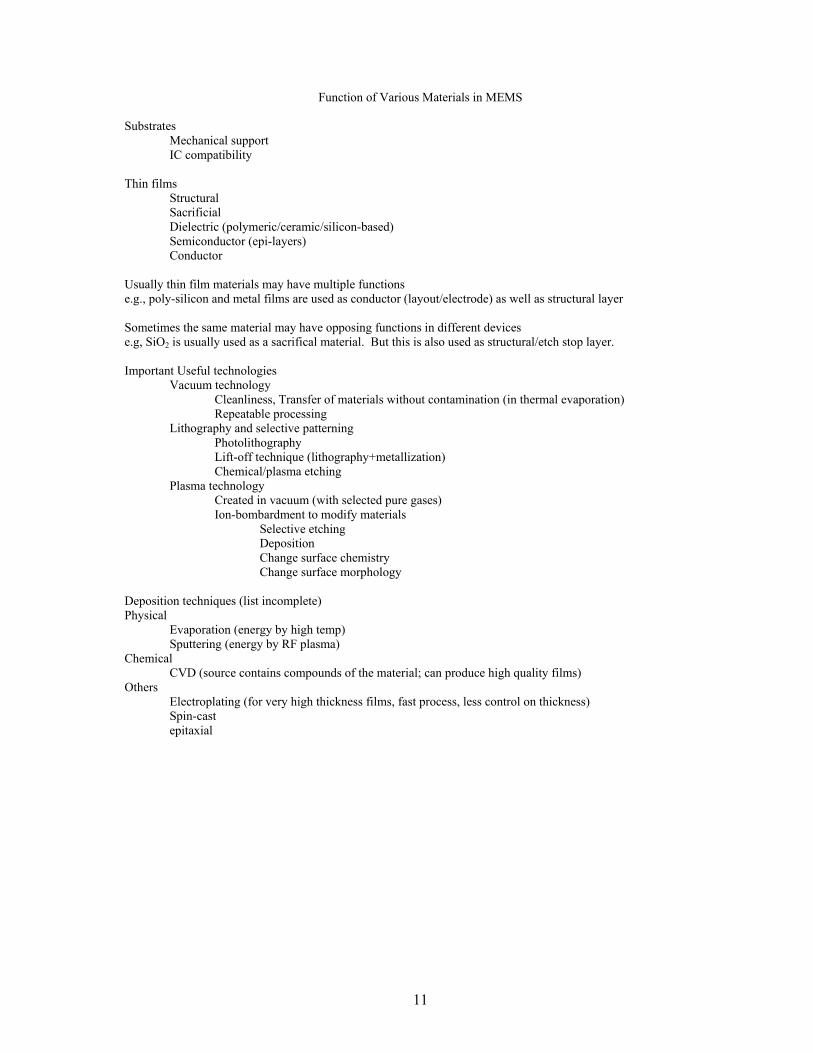
Function of Various Materials in MEMS
Substrates Mechanical support IC compatibility Thin films Structural Sacrificial Dielectric (polymeric/ceramic/silicon-based) Semiconductor (epi-layers)
Conductor Usually thin film materials may have multiple functions e.g., poly-silicon and metal films are used as conductor (layout/electrode) as well as structural layer Sometimes the same material may have opposing functions in different devices e.g, SiO2 is usually used as a sacrifical material. But this is also used as structural/etch stop layer. Important Useful technologies
Vacuum technology Cleanliness, Transfer of materials without contamination (in thermal evaporation) Repeatable processing Lithography and selective patterning Photolithography Lift-off technique (lithography+metallization) Chemical/plasma etching Plasma technology Created in vacuum (with selected pure gases) Ion-bombardment to modify materials Selective etching Deposition Change surface chemistry Change surface morphology
Deposition techniques (list incomplete) Physical Evaporation (energy by high temp) Sputtering (energy by RF plasma) Chemical CVD (source contains compounds of the material; can produce high quality films) Others Electroplating (for very high thickness films, fast process, less control on thickness) Spin-cast epitaxial
12
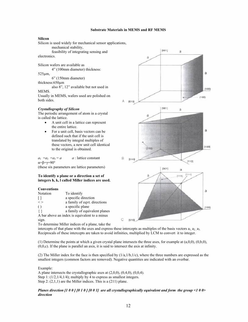
Substrate Materials in MEMS and RF MEMS
Silicon Silicon is used widely for mechanical sensor applications,
mechanical stability, feasibility of integrating sensing and
electronics. Silicon wafers are available as
4” (100mm diameter) thickness: 525µm,
6” (150mm diameter) thickness:650µm
also 8”, 12” available but not used in MEMS. Usually in MEMS, wafers used are polished on both sides. Crystallography of Silicon The periodic arrangement of atom in a crystal is called the lattice.
• A unit cell in a lattice can represent the entire lattice.
• For a unit cell, basis vectors can be defined such that if the unit cell is translated by integral multiples of these vectors, a new unit cell identical to the original is obtained.
a1 =a2 =a3 = a a : lattice constant α=β=γ=90° (these six parameters are lattice parameters) To identify a plane or a direction a set of integers h, k, l called Miller indices are used. Conventions Notation To identify [ ] a specific direction < > a family of eqvt. directions ( ) a specific plane a family of equivalent planes A bar above an index is equivalent to a minus sign. To determine Miller indices of a plane, take the intercepts of that plane with the axes and express these intercepts as multiples of the basis vectors a1, a2 , a3. Reciprocals of these intercepts are taken to avoid infinities, multiplied by LCM to convert it to integer. (1) Determine the points at which a given crystal plane intersects the three axes, for example at (a,0,0), (0,b,0), (0,0,c). If the plane is parallel an axis, it is said to intersect the axis at infinity. (2) The Miller index for the face is then specified by (1/a,1/b,1/c), where the three numbers are expressed as the smallest integers (common factors are removed). Negative quantities are indicated with an overbar. Example: A plane intersects the crystallographic axes at (2,0,0), (0,4,0), (0,0,4). Step 1: (1/2,1/4,1/4); multiply by 4 to express as smallest integers. Step 2: (2,1,1) are the Miller indices. This is a (211) plane. Planes direction [1 0 0 ] [0 1 0 ] [0 0 1] are all crystallographically equivalent and form the group <1 0 0> direction
13
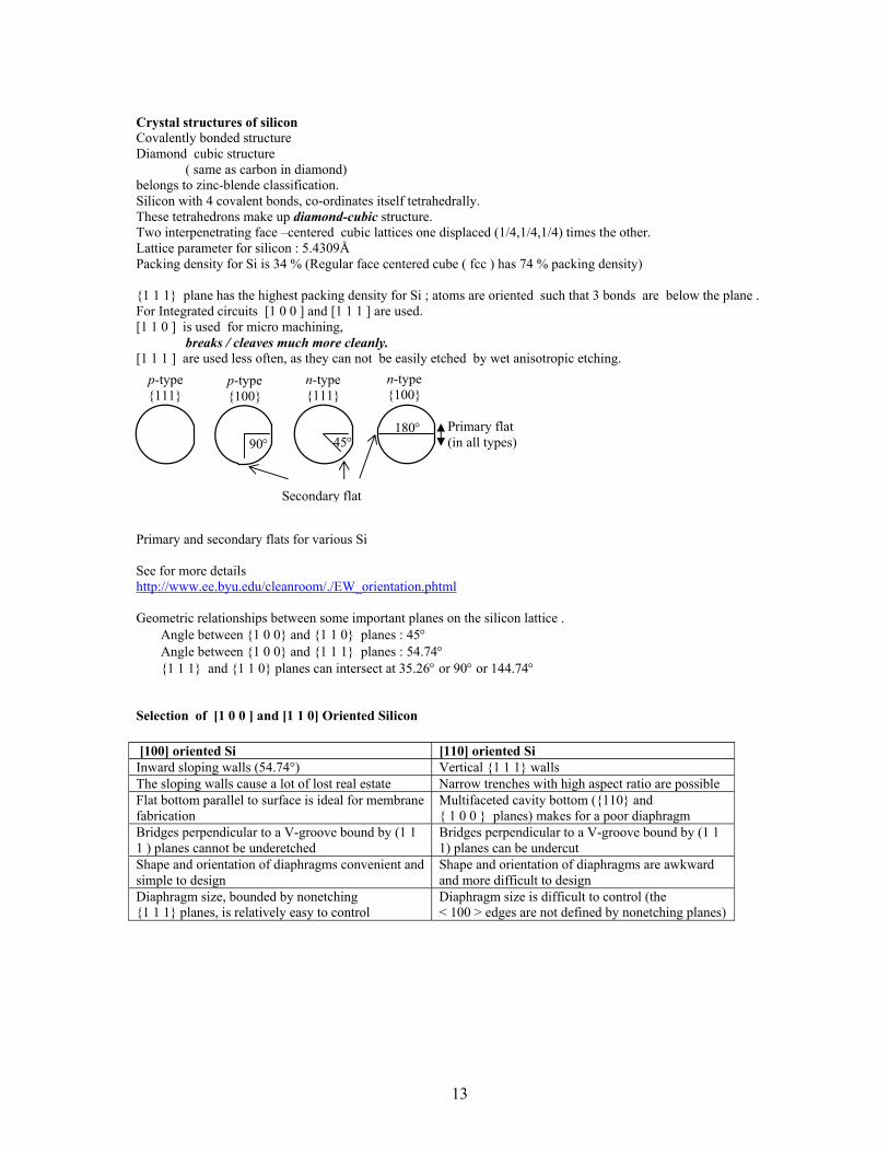
Crystal structures of silicon Covalently bonded structure Diamond cubic structure
( same as carbon in diamond) belongs to zinc-blende classification. Silicon with 4 covalent bonds, co-ordinates itself tetrahedrally. These tetrahedrons make up diamond-cubic structure. Two interpenetrating face –centered cubic lattices one displaced (1/4,1/4,1/4) times the other. Lattice parameter for silicon : 5.4309Å Packing density for Si is 34 % (Regular face centered cube ( fcc ) has 74 % packing density) 1 1 1 plane has the highest packing density for Si ; atoms are oriented such that 3 bonds are below the plane . For Integrated circuits [1 0 0 ] and [1 1 1 ] are used. [1 1 0 ] is used for micro machining,
breaks / cleaves much more cleanly. [1 1 1 ] are used less often, as they can not be easily etched by wet anisotropic etching.
Primary and secondary flats for various Si See for more details http://www.ee.byu.edu/cleanroom/./EW_orientation.phtml Geometric relationships between some important planes on the silicon lattice .
Angle between 1 0 0 and 1 1 0 planes : 45° Angle between 1 0 0 and 1 1 1 planes : 54.74° 1 1 1 and 1 1 0 planes can intersect at 35.26° or 90° or 144.74°
Selection of [1 0 0 ] and [1 1 0] Oriented Silicon [100] oriented Si [110] oriented Si Inward sloping walls (54.74°) Vertical 1 1 1 walls The sloping walls cause a lot of lost real estate Narrow trenches with high aspect ratio are possible Flat bottom parallel to surface is ideal for membrane fabrication
Multifaceted cavity bottom (110 and 1 0 0 planes) makes for a poor diaphragm
Bridges perpendicular to a V-groove bound by (1 1 1 ) planes cannot be underetched
Bridges perpendicular to a V-groove bound by (1 1 1) planes can be undercut
Shape and orientation of diaphragms convenient and simple to design
Shape and orientation of diaphragms are awkward and more difficult to design
Diaphragm size, bounded by nonetching 1 1 1 planes, is relatively easy to control
Diaphragm size is difficult to control (the < 100 > edges are not defined by nonetching planes)
p-type 111
p-type 100
n-type 100
n-type 111
Primary flat (in all types)
Secondary flat
90° 45° 180°
14
Anisotropically etched features in a (100) wafer with a square mask (pyramidal pit) and rectangular mask (V groove)
note: the (100) bottom plane disappears by continuous etching
normally, no under etching occurs if the mask is not aligned, undercutting will occur. For a mask opening of arbitrary opening and orientation, etching for sufficiently long time can result in
pyramidal structures/grooves Convex corners (>180) in the mask will be undercut. This property can be made to use in designing suspended cantilever/bridge structure
Standard Dimensions of a Si Wafer
Wafer diameter Parameter
100 mm (4″) 125 mm (5″) 150 mm (6″)
Primary flat length (mm) 30 to 35 40 to 45 55 to 60 Secondary flat length (mm) 16 to 20 25 to 30 35 to 40 Bow (mm) 60 70 60 Total thickness variation (µm) 50 65 50 Surface orientation (100) or (111) (100) or (111) (100) or (111)
Disadvantages of silicon Silicon is not usually used in these cases:
For large device size. Low production volume. When electronics is not needed or cannot be integrated.
Important useful characteristics of silicon Sensory
Piezo resistivity in silicon. Thermal properties of Si Optical properties of Si
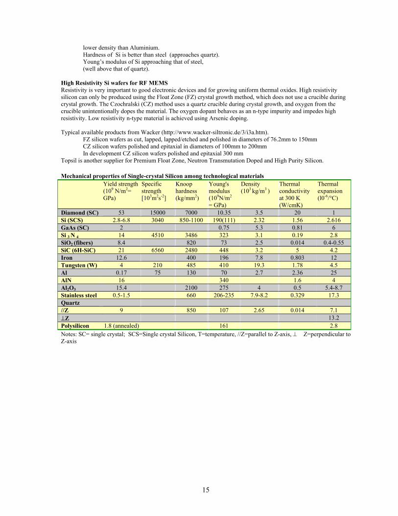
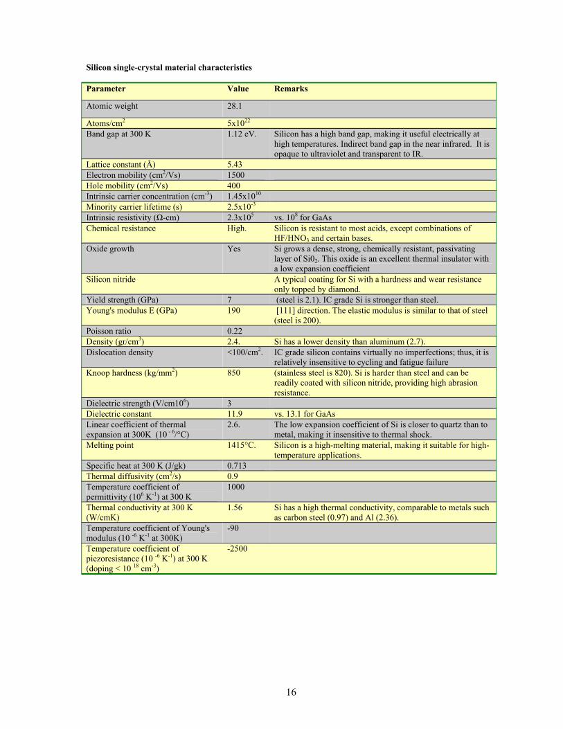
Mechanical Si has better yield strength than steel
15
lower density than Aluminium. Hardness of Si is better than steel (approaches quartz). Young’s modulus of Si approaching that of steel, (well above that of quartz).
High Resistivity Si wafers for RF MEMS Resistivity is very important to good electronic devices and for growing uniform thermal oxides. High resistivity silicon can only be produced using the Float Zone (FZ) crystal growth method, which does not use a crucible during crystal growth. The Czochralski (CZ) method uses a quartz crucible during crystal growth, and oxygen from the crucible unintentionally dopes the material. The oxygen dopant behaves as an n-type impurity and impedes high resistivity. Low resistivity n-type material is achieved using Arsenic doping. Typical available products from Wacker (http://www.wacker-siltronic.de/3/i3a.htm).
FZ silicon wafers as cut, lapped, lapped/etched and polished in diameters of 76.2mm to 150mm CZ silicon wafers polished and epitaxial in diameters of 100mm to 200mm In development CZ silicon wafers polished and epitaxial 300 mm
Topsil is another supplier for Premium Float Zone, Neutron Transmutation Doped and High Purity Silicon. Mechanical properties of Single-crystal Silicon among technological materials Yield strength
Intrinsic resistivity (Ω-cm) 2.3x10⁵ vs. 108 for GaAs Chemical resistance High. Silicon is resistant to most acids, except combinations of
HF/HNO3 and certain bases. Oxide growth Yes Si grows a dense, strong, chemically resistant, passivating
layer of Si02. This oxide is an excellent thermal insulator with a low expansion coefficient
Silicon nitride A typical coating for Si with a hardness and wear resistance only topped by diamond.
Yield strength (GPa) 7 (steel is 2.1). IC grade Si is stronger than steel. Young's modulus E (GPa) 190 [111] direction. The elastic modulus is similar to that of steel
(steel is 200). Poisson ratio 0.22 Density (gr/cm3) 2.4. Si has a lower density than aluminum (2.7). Dislocation density <100/cm2. IC grade silicon contains virtually no imperfections; thus, it is
relatively insensitive to cycling and fatigue failure Knoop hardness (kg/mm2) 850 (stainless steel is 820). Si is harder than steel and can be
readily coated with silicon nitride, providing high abrasion resistance.
Dielectric strength (V/cm106) 3 Dielectric constant 11.9 vs. 13.1 for GaAs Linear coefficient of thermal expansion at 300K (10 - 6/°C)
2.6. The low expansion coefficient of Si is closer to quartz than to metal, making it insensitive to thermal shock.
Melting point 1415°C. Silicon is a high-melting material, making it suitable for high-temperature applications.
Specific heat at 300 K (J/gk) 0.713 Thermal diffusivity (cm2/s) 0.9 Temperature coefficient of permittivity (106 K-1) at 300 K
1000
Thermal conductivity at 300 K (W/cmK)
1.56 Si has a high thermal conductivity, comparable to metals such as carbon steel (0.97) and Al (2.36).
Temperature coefficient of Young's modulus (10 -6 K-1 at 300K)
-90
Temperature coefficient of piezoresistance (10 -6 K-1) at 300 K (doping < 10 18 cm-3)
-2500
17
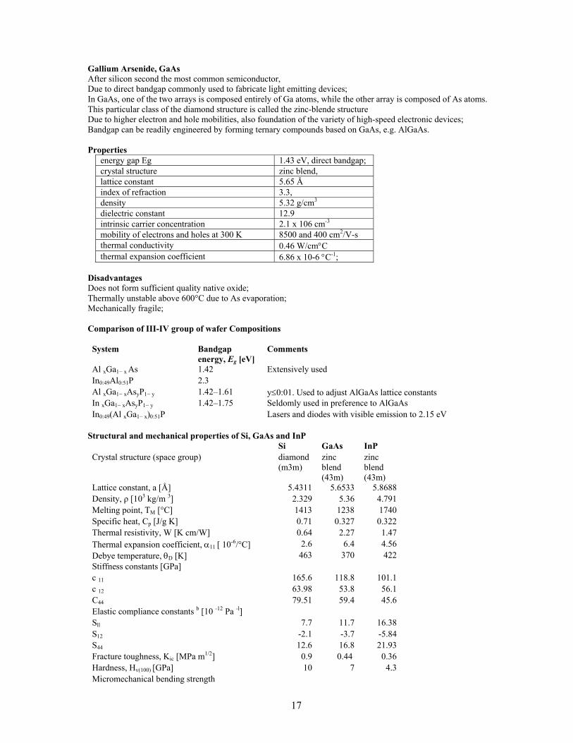
Gallium Arsenide, GaAs After silicon second the most common semiconductor, Due to direct bandgap commonly used to fabricate light emitting devices; In GaAs, one of the two arrays is composed entirely of Ga atoms, while the other array is composed of As atoms. This particular class of the diamond structure is called the zinc-blende structure Due to higher electron and hole mobilities, also foundation of the variety of high-speed electronic devices; Bandgap can be readily engineered by forming ternary compounds based on GaAs, e.g. AlGaAs. Properties
energy gap Eg 1.43 eV, direct bandgap; crystal structure zinc blend, lattice constant 5.65 Å index of refraction 3.3, density 5.32 g/cm3 dielectric constant 12.9 intrinsic carrier concentration 2.1 x 106 cm-3 mobility of electrons and holes at 300 K 8500 and 400 cm2/V-s thermal conductivity 0.46 W/cm°C thermal expansion coefficient 6.86 x 10⁻⁶ °C-1;
Disadvantages Does not form sufficient quality native oxide; Thermally unstable above 600°C due to As evaporation; Mechanically fragile; Comparison of III-IV group of wafer Compositions System Bandgap
energy, Eg [eV] Comments
Al xGa1− x As 1.42 Extensively used In0:49Al0:51P 2.3 Al xGa1− xAsyP1− y 1.42–1.61 y≤0:01. Used to adjust AlGaAs lattice constants In xGa1− xAsyP1− y 1.42–1.75 Seldomly used in preference to AlGaAs In0:49(Al xGa1− x)0:51P Lasers and diodes with visible emission to 2.15 eV
Structural and mechanical properties of Si, GaAs and InP Si GaAs InP Crystal structure (space group) diamond
aTemperature and pressure dependent values are given for RT and 1 atm. bThe values for silicon have been calculated from the cij values, using the relationships: c11-c12= (s11-s12)-1 , c11+2c12=(s11+2s12)-1 and c44= (s44)-1. c Calculated from σf= 1.6Klc(πc)-1/2, assuming the same defect distribution as in GaAs. Other Substrate Materials Glass Fused Quartz
This is naturally occurring crystalline silica (Silicon Dioxide) from stone, sand, rock or lumps in its melted form. Density (at 20º C): 2.2 g/cm3; Thermal Coefficient of Expansion: 5.5 x 10⁻⁷/°C; Strain Point: 1120°C; Refractive Index: 1.458; Dielectric Constant: 3.75.
Fused Silica
Density (at 20º C): 2.2 g/cm3; Thermal Coefficient of Expansion: 5.5 x 10⁻⁷/°C; Strain Point: 990°C; Annealing Point: 1075°C; Softening Point: 1585°C; Refractive Index(l=589.3nm): 1.459; Dielectric Constant: 3.8
Performance of various substrates (for general MEMS / IC applications)
Substrate cost Metallization Machinability Ceramic medium Fair poor plastic low Poor fair silicon high Good Very good glass low Good poor
Comparison of Various Substrate materials useful in RF MEMS