Microwave Wideband Synthesizer with Integrated VCO
Data Sheet ADF4372
Rev. 0 Document Feedback Information furnished by Analog Devices is believed to be accurate and reliable. However, no responsibility is assumed by Analog Devices for its use, nor for any infringements of patents or other rights of third parties that may result from its use. Specifications subject to change without notice. No license is granted by implication or otherwise under any patent or patent rights of Analog Devices. Trademarks and registered trademarks are the property of their respective owners.
FEATURES RF output frequency range: 62.5 MHz to 16,000 MHz Fractional-N synthesizer and integer-N synthesizer High resolution 39-bit fractional modulus Typical spurious fPFD: −90 dBc Integrated rms jitter: 38 fs (1 kHz to 100 MHz) Normalized phase noise floor: −234 dBc/Hz fPFD operation to 250 MHz Reference input frequency operation to 600 MHz Programmable divide by 1, 2, 4, 8, 16, 32, or 64 output 62.5 MHz to 8,000 MHz output at RF8x and RFAUX8x 8,000 MHz to 16,000 MHz output at RF16x Lock time approximately 3 ms with automatic calibration Lock time <30 μs with autocalibration bypassed, typical Analog and digital power supplies: 3.3 V typical VCO supply voltage: 3.3 V and 5 V RF output mute function 7mm × 7mm, 48-terminal LGA package
APPLICATIONS Wireless infrastructure (multicarrier global system for
mobile communication (MC-GSM), 5G) Test equipment and instrumentation Clock generation Aerospace and defense
GENERAL DESCRIPTION The ADF4372 allows implementation of fractional-N or integer-N phase-locked loop (PLL) frequency synthesizers when used with an external loop filter and an external reference frequency. The wideband microwave voltage controlled oscillator (VCO) design allows frequencies from 62.5 MHz to 16 GHz to be generated.
The ADF4372 has an integrated VCO with a fundamental output frequency ranging from 4000 MHz to 8000 MHz. In addition, the VCO frequency is connected to a divide by 1, 2, 4, 8, 16, 32, or 64 circuit that allows the user to generate radio frequency (RF) output frequencies as low as 62.5 MHz at RF8x. A frequency multiplier at RF16x generates from 8 GHz to 16 GHz. RFAUX8x duplicates the frequency range of RF8x or permits direct access to the VCO output. To suppress the unwanted products of frequency multiplication, a harmonic filter exists between the multiplier and the output stage of RF16x.
Control of all on-chip registers is through a 3-wire interface. The ADF4372 operates with analog and digital power supplies ranging from 3.15 V to 3.45 V, and 5 V for the VCO power supply. The ADF4372 also contains hardware and software power-down modes.
SPECIFICATIONS 4.75 V ≤ VCC_VCO ≤ 5.25 V, all other supply pins (AVDD) = 3.3 V ± 5%, GND = 0 V, dBm referred to 50 Ω, TA = whole operating temperature range, unless otherwise noted.
Table 1. Parameter Symbol Min Typ Max Unit Test Conditions/Comments REFP AND REFN CHARACTERISTICS
Parameter Symbol Min Typ Max Unit Test Conditions/Comments Output Dividers
Divider = 2 14 20 mA Each divide by 2 consumes additional typical 7 mA current
Divider = 64 50 65 mA VCO Supply Voltage VCC_VCO 3.15 3.3 3.45 V 3.3 V condition 4.75 5 5.25 V 5 V condition VCO Supply Current IVCO 80 120 mA 3.3 V condition 135 180 mA 5 V condition RF8x Supply Current RF8P and RF8N output stage is
programmable, extra current is drawn in VCC_X1
25 mA −4 dBm setting 39 mA −1 dBm setting 52 mA 2 dBm setting 65 mA 5 dBm setting RFAUX8x Supply Current 42 mA −4 dBm setting 56 mA −1 dBm setting 70 mA 2 dBm setting 84 mA 5 dBm setting RF16x Supply Current 90 120 mA Low Power Sleep Mode 5.1 6.2 mA Hardware power-down 3.3 V VCO case 8 9.5 mA Hardware power-down 5 V VCO case 21.5 25 mA Software power-down 3.3 V VCO case
23.7 28 mA Software power-down 5 V VCO case RF OUTPUT CHARACTERISTICS
VCO Frequency Range 4000 8000 MHz Fundamental VCO range RF8P and RF8N Output Frequency 62.5 8000 MHz RFAUX8P and RFAUX8N Output
Frequency 62.5 8000 MHz
RF16P and RF16N Output Frequency 8000 16000 MHz 2 × VCO output VCO Sensitivity KV
For 5 V 80 MHz/V VCO frequency = 6 GHz, see Figure 33 for KV plot
For 3.3 V 60 MHz/V VCO frequency = 6 GHz, see Figure 34 for KV plot
Frequency Pushing (Open-Loop) 8 MHz/V Frequency Pulling (Open-Loop) 0.5 MHz Voltage standing wave ratio (VSWR) = 2:1
RF8P and RF8N 30 MHz VSWR = 2:1 RF16x Maintain Lock Temperature Range2 125 °C Maintains lock without reprogramming
device Harmonic Content
Second Harmonic RF8P and RF8N −25 dBc Fundamental VCO output (RF8x) −25 dBc Divided VCO output (RF8x) Third Harmonic RF8P and RF8N −12 dBc Fundamental VCO output RF8x) −15 dBc Divided VCO output (RF8x) Second Harmonic RF16P and RF16N −30 dBc Measured at 20 GHz Third Harmonic RF16P and RF16N −30 dBc Measured at 30 GHz
Fundamental VCO Feedthrough −62 dBc RF16x = 10 GHz, VCO frequency = 5 GHz −30 dBc RF8P and RF8N = 1 GHz,
VCO frequency = 4 GHz RF Output Power Maximum Setting3 7 dBm RF8P = 4 GHz, 7.5 nH inductor to VCC_X1 5 dBm RF8P = 8 GHz, 7.5 nH inductor to VCC_X1 0 dBm RF16x = 8 GHz
Parameter Symbol Min Typ Max Unit Test Conditions/Comments 4 dBm RF16x = 16 GHz RF Output Power Variation ±1 dB RF8P and RF8N = 5 GHz ±1 dB RF16x = 10 GHz RF Output Power Variation (Over
Frequency) ±2 dB RF8x and RFAUX8x = 4 GHz to 8 GHz
±2.5 dB RF16x = 8 GHz to 16 GHz Level of Signal with RF Output Disabled −50 dBm RF8P and RF8N = 1 GHz −44 dBm RF8P and RF8N = 8 GHz −41 dBm RF8P and RF8N = 8 GHz, 5 V VCO case −75 dBm RF16P = 8 GHz −55 dBm RF16P = 16 GHz
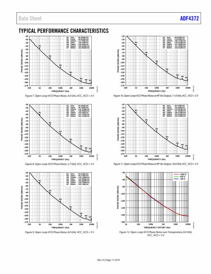
NOISE CHARACTERISTICS Fundamental VCO Phase Noise
Performance where VCC VCO = 5 V VCO noise in open-loop conditions,
VCC_VCO = 5 V −117 dBc/Hz 100 kHz offset from 4.0 GHz carrier −139 dBc/Hz 1 MHz offset from 4.0 GHz carrier −156 dBc/Hz 10 MHz offset from 4.0 GHz carrier −112 dBc/Hz 100 kHz offset from 5.7 GHz carrier −136 dBc/Hz 1 MHz offset from 5.7 GHz carrier −153 dBc/Hz 10 MHz offset from 5.7 GHz carrier −109 dBc/Hz 100 kHz offset from 8.0 GHz carrier −133 dBc/Hz 1 MHz offset from 8.0 GHz carrier −152 dBc/Hz 10 MHz offset from 8.0 GHz carrier RF16x Output Phase Noise Performance
where VCC_VCO = 5 V VCC_VCO = 5 V
−106 dBc/Hz 100 kHz offset from 11.4 GHz carrier −130 dBc/Hz 1 MHz offset from 11.4 GHz carrier −146 dBc/Hz 10 MHz offset from 11.4 GHz carrier −103 dBc/Hz 100 kHz offset from 16 GHz carrier −127 dBc/Hz 1 MHz offset from 16 GHz carrier −145 dBc/Hz 10 MHz offset from 16 GHz carrier Fundamental VCO Phase Noise
Performance where VCC_VCO = 3.3 V VCO noise in open-loop conditions,
VCC_VCO = 3.3 V −116 dBc/Hz 100 kHz offset from 4.0 GHz carrier −137 dBc/Hz 1 MHz offset from 4.0 GHz carrier −156 dBc/Hz 10 MHz offset from 4.0 GHz carrier −111 dBc/Hz 100 kHz offset from 5.7 GHz carrier −133 dBc/Hz 1 MHz offset from 5.7 GHz carrier −153 dBc/Hz 10 MHz offset from 5.7 GHz carrier −109 dBc/Hz 100 kHz offset from 8.0 GHz carrier −132 dBc/Hz 1 MHz offset from 8.0 GHz carrier −153 dBc/Hz 10 MHz offset from 8.0 GHz carrier Normalized Inband Phase Noise Floor
Parameter Symbol Min Typ Max Unit Test Conditions/Comments FREQUENCY LOCK TIME7
Lock Time with Automatic Calibration 3 ms Lock Time with Automatic Calibration
Bypassed 30 µs
1 TA = 25°C, AVDD = 3.3 V, VCC_VCO = 5.0 V, prescaler = 4/5, reference frequency (fREFP) = 50 MHz, fPFD = 50 MHz, and RF frequency (fRF) = 5001 MHz. RF8x enabled. All RF
outputs are disabled. 2 Guaranteed by design and characterization. 3 RF output power using the EV-ADF4372SD2Z differential outputs combined using a Marki BAL-0036 balun, and measured by a spectrum analyzer with the evaluation
board and cable losses de-embedded. Highest power output selected for RF8P, RF8N, RFAUX8P, and RFAUX8N. 4 Use this value to calculate the phase noise for any application. To calculate inband phase noise performance as seen at the VCO output, use the following formula: −233 +
10log(fPFD) + 20logN. The result is the lowest noise mode for the fractional channel. 5 Use this value to calculate the phase noise for any application. To calculate inband phase noise performance as seen at the VCO output, use the following formula: −234 +
10log(fPFD) + 20logN. The result is the lowest noise mode for the integer channel. 6 The PLL phase noise is composed of 1/f (flicker) noise plus the normalized PLL noise floor. The formula for calculating the 1/f noise contribution at a radio frequency
(fRF) and at a frequency offset (fOFFSET) is given by PN1_f + 10log(10 kHz/fOFFSET) + 20log(fRF/1 GHz). Both the normalized phase noise floor and flicker noise are modeled in the ADIsimPLL design tool.
7 Lock time is measured for 100 MHz jump with standard evaluation board configuration.
TIMING SPECIFICATIONS
Table 2. Parameter Symbol Test Conditions/Comments Min Typ Max Unit Serial Port Interface (SPI) Timing See Figure 2, Figure 3, and Figure 4
SCLK Frequency fSCLK 50 MHz SCLK Period tSCLK 20 ns SCLK Pulse Width High tHIGH 10 ns SCLK Pulse Width Low tLOW 10 ns SDIO Setup Time tDS 2 ns SDIO Hold Time tDH 2 ns SCLK Falling Edge to SDIO Valid Propagation
ABSOLUTE MAXIMUM RATINGS TA = 25°C, unless otherwise noted.
Table 3. Parameter Rating AVDD Rails to GND1 −0.3 V to +3.6 V AVDD Rails to Each Other −0.3 V to +0.3 V VCC_VCO to GND1 −0.3 V to +5.5 V VCC_VCO to AVDD −0.3 V to AVDD + 2.8 V CPOUT to GND1 −0.3 V to AVDD + 0.3 V VTUNE to GND −0.3 V to AVDD + 0.3 V Digital Input and Output Voltage to
GND1 −0.3 V to AVDD + 0.3 V
Analog Input and Output Voltage to GND1
−0.3 V to AVDD + 0.3 V
REFP and REFN to GND1 −0.3 V to AVDD + 0.3 V REFP to REFN ±2.1 V Temperature
Operating Range −40°C to +105°C Storage Range −65°C to +125°C Maximum Junction 125 °C Reflow Soldering
Peak 260°C Time at Peak 30 sec
Electrostatic Discharge (ESD) Charged Device Model 1.0 kV Human Body Model 4.0 kV
Transistor Count Complementary Metal-Oxide
Semiconductor (CMOS) 131,439
Bipolar 4063 1 GND = 0 V.
Stresses at or above those listed under Absolute Maximum Ratings may cause permanent damage to the product. This is a stress rating only; functional operation of the product at these or any other conditions above those indicated in the operational section of this specification is not implied. Operation beyond the maximum operating conditions for extended periods may affect product reliability.
THERMAL RESISTANCE Thermal performance is directly linked to printed circuit board (PCB) design and operating environment. Close attention to PCB thermal design is required.
θJA is the natural convection, junction to ambient thermal resistance measured in a one cubic foot sealed enclosure. θJC is the junction to case thermal resistance.
Table 4. Thermal Resistance Package Type θJA θJC Unit CC-48-41 25 14.4 °C/W 1 Test Condition 1: thermal impedance simulated values are based on JESD51
2 CPOUT Charge Pump (CP) Output. When enabled, this output provides ±ICP to the external loop filter. The output of the loop filter is connected to VTUNE to drive the internal VCO.
3 RS_SW Loop Filter Switch. Used for switching loop filter resistors in fast lock applications. 4 VCC_CAL Power Supply for Internal Calibration Monitor Circuit. The voltage on this pin ranges from 3.15 V to
3.45 V. VCC_CAL must have the same value as AVDD, nominally 3.3 V. 5 VTUNE Control Input to the VCO. This voltage determines the output frequency and is derived from filtering
the CPOUT output voltage. 6 VCC_REG_OUT VCO Supply Regulator Out. The output supply voltage of the VCO regulator is available at this pin, and
must be decoupled to GND with a 10 μF capacitor and shorted to the VCC_VCO pin. Leave this pin open if an external LDO regulator is connected to VCC_VCO.
7 VCC_VCO Power Supply for the VCO. The voltage on this pin ranges from 4.75 V to 5.25 V. Place decoupling capacitors to the analog ground plane as close to this pin as possible. For optimal performance, this supply must be clean and have low noise.
8 VCC_LDO Supply Pin to the VCO Regulator. If the internal regulator is used, connect the voltage supply to VCC_LDO. The voltage on this pin ranges from 4.75 V to 5.25 V. If the external regulator is used, short this pin to VCC_VCO.
10, 11 NC No Connect. 14, 16 VCC_X1 Power Supply for the Main RF Output. The voltage on this pin must have the same value as AVDD. 15, 17 VDD_X1 Digital Supply for the Main RF Circuit. The voltage on this pin must have the same value as AVDD. 18 RF8P Main RF Output. AC couple to the next stage. The output level is programmable. The VCO fundamental
output or a divided down version is available. 19 RF8N Complementary Main RF Output. AC couple this pin to the next stage. The output level is
programmable. The VCO fundamental output or a divided down version is available. 21 VCC_X2 Power Supply for the Doubled RF Output. The voltage on this pin must have the same value as AVDD. 22 RFAUX8P Auxiliary RF Output. AC couple to the next stage. This pin can be powered off when not in use. 23 RFAUX8N Complementary Auxiliary RF Output. AC couple this pin to the next stage. This pin can be powered off
when not in use. 26 RF16P Doubled VCO Output. AC or dc couple this pin to the next stage. This pin can be powered off when not
in use. If unused, this pin can be left open. 27 RF16N Complementary Doubled VCO Output. AC or dc couple this pin to the next stage. This pin can be
powered off when not in use. If unused, this pin can be left open.
Pin No. Mnemonic Description 29 VCC_MUX Power Supply for the VCO Mux. The voltage on this pin must have the same value as AVDD. 30 VCC_3V Analog Power Supply. The voltage on this pin must have the same value as AVDD. 31 VDD_NDIV N Divider Power Supply. The voltage on this pin must have the same value as AVDD. 32 VDD_LS Level Shifter Power Supply. The voltage on this pin must have the same value as AVDD. 33 CS Chip Select, CMOS Input. When CS goes high, the data stored in the shift register is loaded into the
register that is selected by the address bits. 34 SDIO Serial Data Input Output. This input is a high impedance CMOS input. 35 SCLK Serial Clock Input. Data is clocked into the 24-bit shift register on the clock rising (or falling) edge. This
input is a high impedance CMOS input. 38 VCC_LDO_3V Regulator Input for 1.8 V Digital Logic. The voltage on this pin must have the same value as AVDD. 39 CE Chip Enable. Connect to 3.3 V or AVDD. 40 TEST Factory Test Pin. Connect this pin to ground. 41 MUXOUT Mux Output. The mux output allows the digital lock detect, the analog lock detect, scaled RF, or the
scaled reference frequency to be externally accessible. This pin can be programmed to output the register settings in 4-wire SPI mode.
43 REFP Reference Input. If driving the device with a single-ended reference, ac couple the signal to the REFP pin.
44 REFN Complementary Reference Input. If unused, ac couple this pin to GND. REFP and REFN must be ac-coupled if driven differentially. If driven single-ended, the reference signal must be connected to REFP, and the REFN must be ac-coupled to GND. In differential configuration, the differential impedance is 100 Ω.
45 VCC_REF Power Supply to the Reference Buffer. The voltage on this pin must have the same value as AVDD. 46 VDD_PFD Power Supply to the Phase Frequency Detector (PFD). The voltage on this pin must have the same
value as AVDD. 47 VDD_VP Charge Pump Power Supply. The voltage on this pin must have the same value as AVDD. A 1 μF
decoupling capacitor to GND must be included to minimize spurious signals. EP Exposed Pad. The land grid array (LGA) has an exposed pad that must be soldered to a metal plate on
THEORY OF OPERATION RF SYNTHESIZER, A WORKED EXAMPLE Use the following equations to program the ADF4372 synthesizer:
PFDRFOUT
FRAC2FRAC1 fMOD2f INTMOD1 RF Divider
+ = + ×
(1)
where: fRFOUT is the RF output frequency. INT is the integer division factor. FRAC1 is the fractionality. FRAC2 is the auxiliary fractionality. MOD2 is the auxiliary modulus. MOD1 is the fixed 25-bit modulus. RF Divider is the output divider that divides down the VCO frequency.
fPFD = REFIN × ((1 + D)/(R × (1 + T))) (2)
where: REFIN is the reference frequency input. D is the REFIN doubler bit. R is the reference division factor. T is the reference divide by 2 bit (0 or 1).
For example, in a universal mobile telecommunication system (UMTS) where a 2112.8 MHz fRFOUT is required, a 122.88 MHz REFIN is available. The ADF4372 VCO operates in the frequency range of 4 GHz to 8 GHz. Therefore, the RF divider of 2 must be used (VCO frequency = 4225.6 MHz, fRFOUT = VCO frequency/RF divider = 4225.6 MHz/2 = 2112.8 MHz).
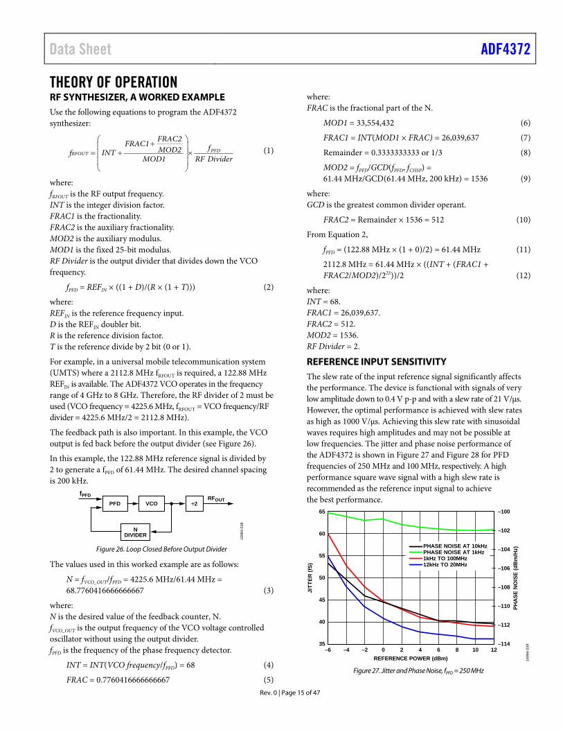
The feedback path is also important. In this example, the VCO output is fed back before the output divider (see Figure 26).
In this example, the 122.88 MHz reference signal is divided by 2 to generate a fPFD of 61.44 MHz. The desired channel spacing is 200 kHz.
fPFD
PFD VCO
NDIVIDER
÷2RFOUT
1698
4-03
8
Figure 26. Loop Closed Before Output Divider
The values used in this worked example are as follows:
N = fVCO_OUT/fPFD = 4225.6 MHz/61.44 MHz = 68.7760416666666667 (3)
where: N is the desired value of the feedback counter, N. fVCO_OUT is the output frequency of the VCO voltage controlled oscillator without using the output divider. fPFD is the frequency of the phase frequency detector.
REFERENCE INPUT SENSITIVITY The slew rate of the input reference signal significantly affects the performance. The device is functional with signals of very low amplitude down to 0.4 V p-p and with a slew rate of 21 V/μs. However, the optimal performance is achieved with slew rates as high as 1000 V/μs. Achieving this slew rate with sinusoidal waves requires high amplitudes and may not be possible at low frequencies. The jitter and phase noise performance of the ADF4372 is shown in Figure 27 and Figure 28 for PFD frequencies of 250 MHz and 100 MHz, respectively. A high performance square wave signal with a high slew rate is recommended as the reference input signal to achieve the best performance.
REFERENCE DOUBLER AND REFERENCE DIVIDER The on-chip reference doubler allows the input reference signal to be doubled. The doubler is useful for increasing the PFD comparison frequency. To improve the noise performance of the system, increase the PFD frequency. Doubling the PFD frequency typically improves noise performance by 3 dB.
The reference divide by 2 divides the reference signal by 2, resulting in a 50% duty cycle PFD frequency.
SPURIOUS OPTIMIZATION AND FAST LOCK Narrow loop bandwidths can filter unwanted spurious signals. However, these bandwidths typically have a long lock time. A wider loop bandwidth achieves faster lock times, but can lead to increased spurious signals inside the loop bandwidth.
OPTIMIZING JITTER For lowest jitter applications, use the highest possible PFD frequency to minimize the contribution of inband noise from the PLL. Set the PLL filter bandwidth such that the inband noise of the PLL intersects with the open-loop noise of the VCO, minimizing the contribution of both to the overall noise.
Use the ADIsimPLL design tool for this task.
Additional Optimization on Loop Filter
The PLL filter is designed to find an optimum bandwidth for the reference, PFD, and VCO noise, depending on the system requirements. In addition to this design, when the Σ-Δ modulator (SDM) is enabled, further optimization may be necessary to filter SDM noise.
Reducing Σ-Δ Modulator Noise
In fractional mode, SDM noise becomes apparent and starts to contribute to overall phase noise. This noise can be reduced to insignificant levels by using a series resistor between the CPOUT pin and the loop filter. Place this resistor close to the CPOUT pin. A reasonable resistor value does not affect the loop bandwidth and phase margin of the designed loop filter. In most cases, 91 Ω gives the best results. This resistor is not required in integer mode (SDM not enabled) or when a narrow-band loop filter is used (SDM noise attenuated).
SPUR MECHANISMS This section describes the two different spur mechanisms that arise with a fractional-N synthesizer and how to minimize them in the ADF4372.
Integer Boundary Spurs
One mechanism for fractional spur creation is the interactions between the RF VCO frequency and the reference frequency. When these frequencies are not integer related (which is the purpose of a fractional-N synthesizer), spur sidebands appear on the VCO output spectrum at an offset frequency that corresponds to the beat note or the difference in frequency between an integer multiple of the reference and the VCO frequency. These spurs are attenuated by the loop filter and are more noticeable on channels close to integer multiples of the reference where the difference frequency can be inside the loop bandwidth.
Reference Spurs
Reference spurs are generally not a problem in fractional-N synthesizers because the reference offset is far outside the loop bandwidth. However, any reference feedthrough mechanism that bypasses the loop can cause a problem. Feedthrough of low levels of on-chip reference switching noise through the prescaler back to the VCO can result in reference spur levels as high as −100 dBc.
LOCK TIME The PLL lock time divides into a number of settings. The total lock time for changing frequencies is the sum of the four separate times: synthesizer lock, VCO band selection, automatic level calibration (ALC), and PLL settling time.
Synthesizer Lock
The synthesizer lock timeout ensures that the VCO calibration DAC, which forces the VCO tune voltage (VTUNE), has settled to a steady value for the band select circuitry. The SYNTH_LOCK_ TIMEOUT bit and the TIMEOUT bits select the length of time the DAC is allowed to settle to the final voltage before the VCO calibration process continues to the next phase (VCO band selection).
The PFD frequency is the clock for this logic, and the duration is set using the following equation:
_ _ 1024
PFD
SYNTH LOCK TIMEEOUT TIMEOUTf
× + (13)
where: SYNTH_LOCK_TIMEOUT is programmed in Address 0x33. TIMEOUT is programmed in Address 0x31 and Address 0x32.
The calculated time must be greater than or equal to 20 µs.
For the SYNTH_LOCK_TIMEOUT bit, the minimum value is 2 and the maximum value is 31. For the TIMEOUT bits, the minimum value is 2 and the maximum value is 1023.
The VCO_BAND_DIV bits (programmed in Address 0x30) and fPFD are used to generate the VCO band selection clock as follows:
_ _PFD
BSCff
VCO BAND DIV= (14)
The calculated time must be less than or equal to 2.4 MHz.
16 clock cycles are required for one VCO core and band calibration step and the total band selection process takes 11 steps, resulting in the following equation:
××
16 _ _11PFD
VCO BAND DIVf
(15)
The minimum value for VCO_BAND_DIV is 1 and the maximum value is 255.
ALC
Use the ALC function to choose the correct bias current in the ADF4372 VCO core. The duration required for VCO bias voltage to settle for each step is set by the following equation:
_ _ 1024
PFD
VCO ALC TIMEOUT TIMEOUTf
× + (16)
where: VCO_ALC_TIMEOUT and TIMEOUT are programmed in Address 0x34, Address 0x32, and Address 0x31.
The calculated time must be greater than or equal to 50 µs.
The total ALC takes 63 steps. Calculate the total duration for ALC as follows:
_ _ 102463PFD
VCO ALC TIMEOUT TIMEOUTf
× +× (17)
The minimum value for VCO_ALC_TIMEOUT is 2 and the maximum value is 31.
PLL Settling Time
The time taken for the loop to settle is inversely proportional to the low-pass filter bandwidth. The settling time is accurately modeled in the ADIsimPLL design tool.
Lock Time, a Worked Example
Assume that fPFD = 61.44 MHz,
VCO_BAND_DIV = Ceiling(fPFD/2,400,000) = 26 (18)
where Ceiling() rounds up to the nearest integer.
SYNTH_LOCK_TIMEOUT × 1024 + TIMEOUT > 1228.8 (19)
VCO_ALC_TIMEOUT × 1024 + TIMEOUT > 3072 (20)
There are several suitable values that meet these criteria. By considering the minimum specifications, the following values are the most suitable:
Much faster lock times than those detailed in this data sheet are possible by bypassing the calibration processes. Contact an Analog Devices, Inc., sales representative for more information.
CIRCUIT DESCRIPTION REFERENCE INPUT Figure 29 shows the reference input stage. The reference input can accept both single-ended and differential signals. Use the reference mode bit (Bit 6 in Address 0x22) to select the signal. To use a differential signal on the reference input, program this bit high. In this case, SW1 and SW2 are open, SW3 and SW4 are closed, and the current source that drives the differential pair of transistors switches on. The differential signal is buffered, and the signal is provided as an emitter coupled logic (ECL) to the CMOS buffer.
When a single-ended signal is used as the reference, connect the reference signal to REFP and program Bit 6 in Address 0x22 to 0. In this case, SW1 and SW2 are closed, SW3 and SW4 are open, and the current source that drives the differential pair of transistors switches off.
For optimum integer boundary spur and phase noise performance, use the single-ended setting for all references up to 500 MHz (even if using a differential signal). Use the differential setting for reference frequencies greater than 500 MHz.
RF N DIVIDER The RF N divider allows a division ratio in the PLL feedback path. Determine the division ratio by the INT, FRAC1, FRAC2, and MOD2 values that this divider comprises.
THIRD-ORDERFRACTIONAL
INTERPOLATOR
FRAC1VALUE
INTVALUE
RF N COUNTER
FROMVCO OUTPUT OR
OUTPUT DIVIDERS
TO PFDN COUNTER
FRAC2VALUE
MOD2VALUE
1698
4-03
0
Figure 30. RF N Divider
INT, FRAC, MOD, and R Counter Relationship
The INT, FRAC1, FRAC2, MOD1, and MOD2 values, in conjunction with the R counter, make it possible to generate output frequencies that are spaced by fractions of fPFD. For more information, see the RF Synthesizer, a Worked Example section.
Calculate fVCO_OUT using the following equation:
fVCO_OUT = fPFD × N (21)
Calculate fPFD using the following equation:
1
1PFD INDf REF
R T
(22)
where: REFIN is the reference frequency input. D is the REFIN doubler bit. R is the preset divide ratio of the binary 10-bit programmable reference counter (1 to 1023). T is the REFIN divide by 2 bit (0 or 1)
Calculate the desired value of the feedback counter N using the following equation:
FRAC2FRAC1MOD2N INT
MOD1
(23)
where: INT is the 16-bit integer value. In integer mode, INT = 20 to 32,767 for the 4/5 prescaler, and 64 to 65,535 for the 8/9 prescaler. In fractional mode, INT= = 23 to 32,767 for the 4/5 prescaler, and 75 to 65,535 for the 8/9 prescaler. FRAC1 is the numerator of the primary modulus (0 to 33,554,431). FRAC2 is the numerator of the 14-bit auxiliary modulus (0 to 16,383). MOD2 is the programmable, 14-bit auxiliary fractional modulus (2 to 16,383). MOD1 is a 25-bit primary modulus with a fixed value of 225 = 33,554,432.
These calculations result in a very low frequency resolution with no residual frequency error. To apply Equation 23, perform the following steps:
1. Calculate N by dividing VCOOUT/fPFD. The integer value of this number forms INT.
2. Subtract INT from the full N value. 3. Multiply the remainder by 225. The integer value of this
number forms FRAC1. 4. Calculate MOD2 based on the channel spacing (fCHSP)
using the following equation:
MOD2 = fPFD/GCD(fPFD, fCHSP) (24)
where: GCD(fPFD, fCHSP) is the greatest common divisor of the PFD frequency and the channel spacing frequency. fCHSP is the desired channel spacing frequency.
5. Calculate FRAC2 using the following equation:
FRAC2 = ((N – INT) × 225 – FRAC1) × MOD2 (25)
The FRAC2 and MOD2 fraction result in outputs with zero frequency error for channel spacing when
fPFD/GCD(fPFD, fCHSP) = MOD2 < 16,383 (26)
If zero frequency error is not required, the MOD1 and MOD2 denominators operate together to create a 39-bit resolution modulus.
Integer-N Mode
When FRAC1 and FRAC2 are equal to 0, the synthesizer operates in integer-N mode. It is recommended that the SD_EN_FRAC0 bit in Address 0x2B be set to 1 to disable the SDMs, which gives an improvement in the inband phase noise and reduces any additional Σ-Δ noise.
R Counter
The 5-bit R counter allows the input reference frequency (input to REFP and REFN) to be divided down to produce the reference clock to the PFD. Division ratios from 1 to 32 are allowed.
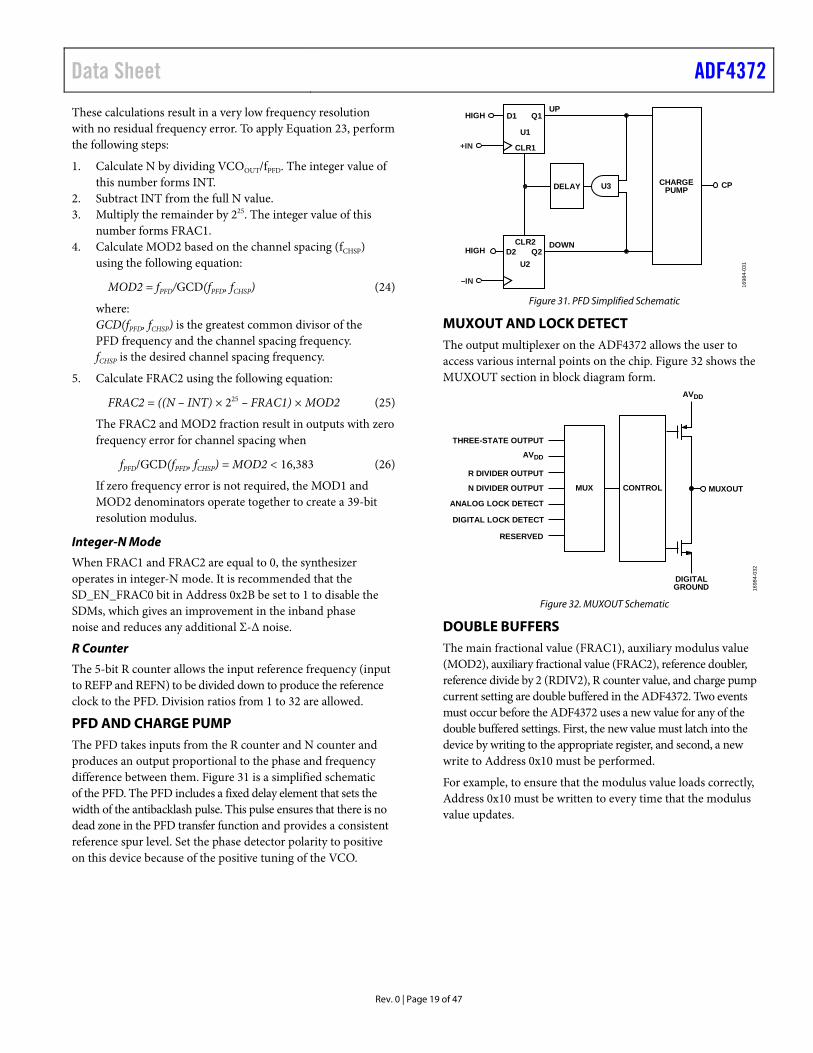
PFD AND CHARGE PUMP The PFD takes inputs from the R counter and N counter and produces an output proportional to the phase and frequency difference between them. Figure 31 is a simplified schematic of the PFD. The PFD includes a fixed delay element that sets the width of the antibacklash pulse. This pulse ensures that there is no dead zone in the PFD transfer function and provides a consistent reference spur level. Set the phase detector polarity to positive on this device because of the positive tuning of the VCO.
U3
CLR2Q2D2
U2
DOWN
UPHIGH
HIGH
CP
–IN
+IN
CHARGEPUMPDELAY
CLR1
Q1D1
U1
1698
4-03
1
Figure 31. PFD Simplified Schematic
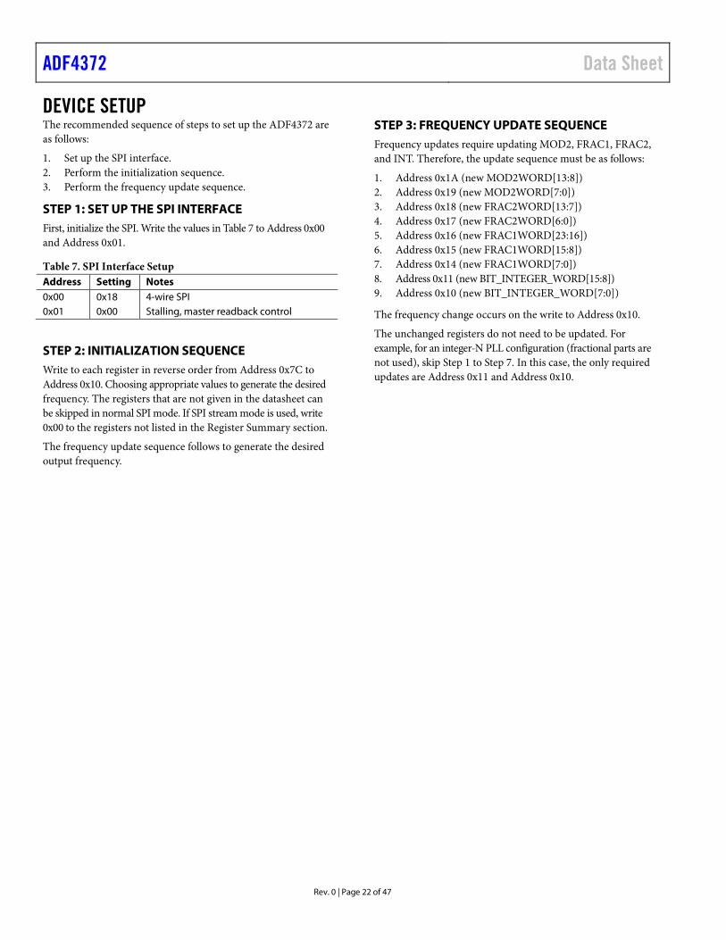
MUXOUT AND LOCK DETECT The output multiplexer on the ADF4372 allows the user to access various internal points on the chip. Figure 32 shows the MUXOUT section in block diagram form.
DIGITALGROUND
AVDD
CONTROLMUX MUXOUT
ANALOG LOCK DETECT
DIGITAL LOCK DETECT
R DIVIDER OUTPUT
N DIVIDER OUTPUT
RESERVED
THREE-STATE OUTPUT
AVDD
1698
4-03
2
Figure 32. MUXOUT Schematic
DOUBLE BUFFERS The main fractional value (FRAC1), auxiliary modulus value (MOD2), auxiliary fractional value (FRAC2), reference doubler, reference divide by 2 (RDIV2), R counter value, and charge pump current setting are double buffered in the ADF4372. Two events must occur before the ADF4372 uses a new value for any of the double buffered settings. First, the new value must latch into the device by writing to the appropriate register, and second, a new write to Address 0x10 must be performed.
For example, to ensure that the modulus value loads correctly, Address 0x10 must be written to every time that the modulus value updates.
VCO The VCO in the ADF4372 consists of four separate VCO cores, Core A, Core B, Core C, and Core D, each of which uses 256 overlapping bands, which allows the device to cover a wide frequency range without large VCO sensitivity (KV) and without resultant poor phase noise and spurious performance.
The correct VCO and band are chosen automatically by the VCO and band select logic whenever Address 0x10 is updated and automatic calibration is enabled. The VCO tune voltage is disconnected from the output of the loop filter and is connected to an internal reference voltage.
The R counter output is used as the clock for the band select logic. After band selection, normal PLL action resumes. The nominal value of KV is 50 MHz/V when the N divider is driven from the VCO output, or the KV value is divided by D. D is the output divider value if the N divider is driven from the RF output divider.
The VCO shows variation of KV as the tuning voltage, VTUNE, varies within the band and from band to band. For wideband applications covering a wide frequency range (and changing output dividers), a value of 50 MHz/V provides the most accurate KV, because this value is closest to the average value. Figure 33 and Figure 34 shows how KV varies with fundamental VCO frequency along with an average value for the frequency band. Users may prefer Figure 33 and Figure 34 when using narrow-band designs.
150
90100110120130140
807060504030201004.0 8.07.57.06.56.05.55.04.5
VCO
SEN
SITI
VITY
, KV
(MH
z/V)
FREQUENCY (GHz) 1698
4-03
3
Figure 33. VCO Sensitivity, KV vs. Frequency, VCC_VCO = 5 V
Figure 34. VCO Sensitivity, KV vs. Frequency, VCC_VCO = 3.3 V
OUTPUT STAGE The RF8P pin and the RF8N pin of the ADF4372 connect to the collectors of a bipolar negative positive negative (NPN) differential pair driven by buffered outputs of the VCO, as shown in Figure 35. The ADF4372 contains internal 50 Ω resistors connected to the VCC_X1 pin. To optimize the power dissipation vs. the output power requirements, the tail current of the differential pair is programmable using Bits[1:0] in Address 0x25. Four current levels can be set. These levels give approximate output power levels of −4 dBm, −1 dBm, 2 dBm, and 5 dBm. Levels of −4 dBm, −1 dBm, and 2 dBm can be achieved by ac coupling into a 50 Ω load. A 5 dBm level requires an external shunt inductor to VCC_X1. An inductor has a narrower operating frequency than a 50 Ω resistor. For accurate power levels, refer to the Typical Performance Characteristics section. Add an external shunt inductor to provide higher power levels, which is less wideband than the internal bias only. Terminate the unused complementary output with a circuit similar to the used output.
VCO
RF8P RF8N
VCC_X1VCC_X1
50Ω 50Ω
BUFFER,DIVIDE BY1, 2, 4, 8,16, 32, 64
1698
4-03
5
Figure 35. Output Stage
The doubled VCO output (8 GHz to 16 GHz) is available on the RF16P pin and the RF16N pin, which can be directly connected to the next circuit. The RFAUX8P and the RFAUX8N provide the same functionality as the RF8x output, but they can output the divided RF8x frequency or the VCO frequency if desired.
DOUBLER The VCO frequency multiplied by 2 is available at the RF16P pin and RF16N pin. This output can be powered down when not in use, and the RF16P pin and the RF16N pin can be left open if unused.
RF16P
×2
RF16N
1698
4-03
6
Figure 36. Doubler Output Stage
An automatic tracking filter on the ADF4372 that suppresses the VCO and other unwanted frequency products ensures the doubled output is maximized and that the VCO and 3 × VCO frequencies are suppressed regardless of the output frequency. Suppression of <50 dB is typical. The optimum values are set automatically by the automatic tracking when it is enabled using Bit 1 in Address 0x23.
The settings for optimum output power, phase noise, and harmonic rejection are given in Table 6.
Table 6. Filter and Bias Settings for Doubled Output Frequency (GHz) Filter Bias
<8.4 7 3 8.4 to 9.4 6 3
9.4 to 10 5 3
10 to 11.5 4 3 11.5 to 12.2 3 3
12.2 to 13.7 2 3
13.7 to 14.5 1 3 >14.5 0 3
OUTPUT STAGE MUTE Another feature of the ADF4372 is that the supply current to the RF8P and RF8N output stage can shut down until the ADF4372 achieves lock as measured by the digital lock detect circuitry. The mute to lock detect bit (MUTE_LD) in Address 0x25 enables this function.
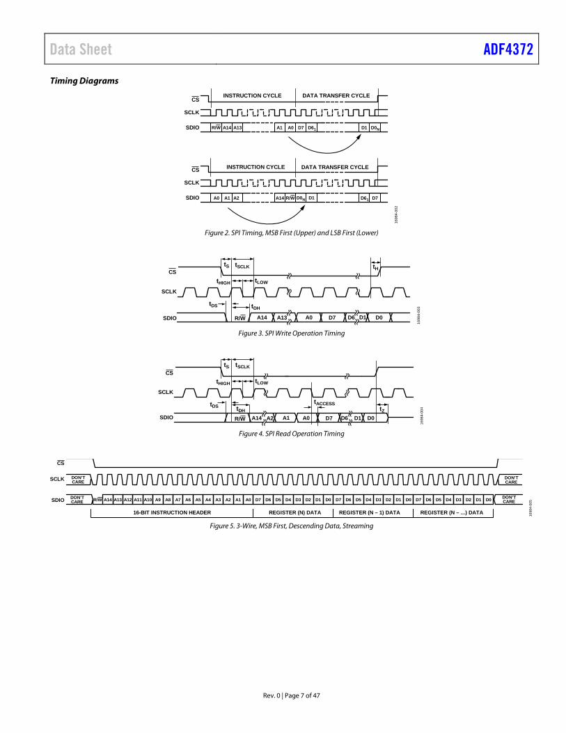
SPI The SPI of the ADF4372 allows the user to configure the device as required via a 3-wire or 4-wire SPI port. This interface provides users with added flexibility and customization. The serial port interface consists of four control lines: SCLK, SDIO, CS, and MUXOUT (not used in 3-wire SPI). The timing requirements for the SPI port are detailed in Table 2.
The SPI protocol consists of a read and write bit and 15 register address bits, followed by eight data bits. Both the address and data fields are organized with the MSB first and end with the LSB by default. The timing diagrams for write mode and read mode are shown in Figure 3 and Figure 4, respectively. The significant bit order can be changed via the Bit 1 (LSB_FIRST) setting at Address 0x00. The related timing diagram is shown in Figure 2.
The ADF4372 input logic level for the write cycle is compatible with 1.8 V logic level (see the logic parameters in Table 1). On a read cycle, both the SDIO pin and MUXOUT pin are configurable for 1.8 V (default) or 3.3 V output levels by the LEV_SEL bit setting.
SPI Stream Mode
The ADF4372 supports stream mode, where data bits are loaded to or read from registers serially without writing the register address (instruction word). This mode is useful in time critical applications, when a large amount of data must be transferred or when some registers must be updated repeatedly.
The slave device starts reading or writing data to this address and continues as long as CS is asserted and single-byte writes are not enabled (Bit 7 in Address 0x01). The slave device automatically increments or decrements the address depending on the setting of the address ascension bit (Bit 2 in Address 0x00).
The diagram of 3-byte streaming is shown in Figure 5. The instruction header starts with a Logic 0 to indicate a write sequence and addresses the register. The data for registers (N, N − 1, and N − 2) are loaded consecutively without any assertion in CS.
The registers are organized into eight bits, and if a register requires more than eight bits, sequential register addresses are used. This organization enables using stream mode and simplifies loading. For example, FRAC1WORD is stored in Address 0x16, Address 0x15, and Address 0x14 (MSB to LSB). These registers can be loaded by using Address 0x16 and sending the whole 24-bit data afterward, as shown in Figure 5.
STEP 2: INITIALIZATION SEQUENCE Write to each register in reverse order from Address 0x7C to Address 0x10. Choosing appropriate values to generate the desired frequency. The registers that are not given in the datasheet can be skipped in normal SPI mode. If SPI stream mode is used, write 0x00 to the registers not listed in the Register Summary section.
The frequency update sequence follows to generate the desired output frequency.
STEP 3: FREQUENCY UPDATE SEQUENCE Frequency updates require updating MOD2, FRAC1, FRAC2, and INT. Therefore, the update sequence must be as follows:
1. Address 0x1A (new MOD2WORD[13:8]) 2. Address 0x19 (new MOD2WORD[7:0]) 3. Address 0x18 (new FRAC2WORD[13:7]) 4. Address 0x17 (new FRAC2WORD[6:0]) 5. Address 0x16 (new FRAC1WORD[23:16]) 6. Address 0x15 (new FRAC1WORD[15:8]) 7. Address 0x14 (new FRAC1WORD[7:0]) 8. Address 0x11 (new BIT_INTEGER_WORD[15:8]) 9. Address 0x10 (new BIT_INTEGER_WORD[7:0])
The frequency change occurs on the write to Address 0x10.
The unchanged registers do not need to be updated. For example, for an integer-N PLL configuration (fractional parts are not used), skip Step 1 to Step 7. In this case, the only required updates are Address 0x11 and Address 0x10.
APPLICATIONS INFORMATION POWER SUPPLIES The ADF4372 contains four multiband VCOs that together cover an octave range of frequencies. To achieve optimal VCO phase noise performance, it is recommended to connect a low noise regulator, such as the ADM7150 or LT3045, to the VCC_VCO pin. Connect the same regulator to the VCC_VCO pin and the VCC_LDO pin. It is recommended to connect 1 μF decoupling capacitors to the 5 V VCO supply.
For all other 3.3 V supply pins, use one ADM7150 or one LT3045 regulator. A 1 μF capacitor is also recommended for the VDD_VP pin. Additional decoupling to other supply pins is not required.
PCB DESIGN GUIDELINES FOR AN LGA PACKAGE The bottom of the chip scale package has a central exposed thermal pad. The thermal pad on the PCB must be at least as large as the exposed pad. On the PCB, there must be a minimum clearance of 0.25 mm between the thermal pad and the inner edges of the pad pattern. This clearance ensures there is no shorting
To improve the thermal performance of the package, use thermal vias on the PCB thermal pad. If vias are used, incorporate them into the thermal pad at the 1.2 mm pitch grid. The via diameter must be between 0.3 mm and 0.33 mm, and the via barrel must be plated with 1 oz. of copper to plug the via into the barrel.
For a microwave PLL and VCO synthesizer, such as the ADF4372, take care with the board stackup and layout. Do not consider using FR4 material because it causes an amplitude decrease in signals greater than 3 GHz. Instead, Rogers 4350, Rogers 4003, or Rogers 3003 dielectric material is suitable.
Take care with the RF output traces to minimize discontinuities and ensure the best signal integrity. Via placement and grounding are critical.
OUTPUT MATCHING The low frequency output can be ac-coupled to the next circuit, if desired. However, if higher output power is required, use a pull-up inductor to increase the output power level.
7.5nH
10pFRF8P
VDD_X1
50Ω
1698
4-04
1
Figure 37. Optimum Output Stage
When differential outputs are not needed, terminate the unused output or combine it with both outputs using a balun.
For lower frequencies that are less than 1 GHz, it is recommended to use a 100 nH inductor on the RF8P pin and the RF8N pin.
The RF8P and RF8N pins form a differential circuit. Provide each output with the same (or similar) components where possible, including the same shunt inductor value, bypass capacitor, and termination.
The RFAUX8P pin and the RFAUX8N pin are effectively the same as the RF8P pin and the RF8N pin and must be treated in the manner as outlined for the RF8P pin and the RF8N pin.
The RF16P pin and the RF16N pin can be directly connected to the next circuit stage. These pins are internally matched to 50 Ω and do not require additional decoupling.
Table 9. Bit Descriptions for REG0000 Bit(s) Bit Name Description Default Access 7 SOFT_RESET_R Copy of Bit 0. 0x0 Read/Write
(R/W) 6 LSB_FIRST_R Copy of Bit 1. 0x0 R/W 5 ADDRESS_ASCENSION_R Copy of Bit 2. 0x0 R/W 4 SDO_ACTIVE_R Copy of Bit 3. 0x1 R/W 3 SDO_ACTIVE Choose Between 3-Pin or 4-Pin Operation. 0x1 R/W 0: 3-pin. 1: 4-pin. Enables SDIO pin and the SDIO pin becomes an input only. 2 ADDRESS_ASCENSION Set Address in Ascending Order (Default Is Ascending). 0x0 R/W 0: descending. 1: ascending. 1 LSB_FIRST Reads LSB First when Active. 0x0 R/W 0 SOFT_RESET Soft Reset. 0x0 R/W 0: normal operation. 1: soft reset.
Table 10. Bit Descriptions for REG0001 Bit(s) Bit Name Description Default Access 7 SINGLE_INSTRUCTION Single Instruction. SPI stream mode is disabled if this bit is set to 1. 0x0 R/W 6 STALLING Stalling. For internal use. 0x0 R/W 5 MASTER_READBACK_CONTROL Master Readback Control. For internal use. 0x0 R/W [4:0] RESERVED Reserved. 0x0 Read
Table 11. Bit Descriptions for REG0003 Bit(s) Bit Name Description Default Access [7:4] RESERVED Reserved. 0x0 R [3:0] CHIP_TYPE Chip Type. 0x0 Read Programmable
(RP)
Address: 0x04, Default: 0xXX, Name: REG0004
Product ID.
0
X1
X2
X3
X4
X5
X6
X7
X
[7:0] PRODUCT_ID[7:0] (R/WP)
Table 12. Bit Descriptions for REG0004 Bit(s) Bit Name Description Default Access [7:0] PRODUCT_ID[7:0] Product ID. 0x0 Read/Write
Programmable (R/WP)
Address: 0x05, Default: 0xXX, Name: REG0005
Product ID.
0
X1
X2
X3
X4
X5
X6
X7
X
[7:0] PRODUCT_ID[15:8] (R/WP)
Table 13. Bit Descriptions for REG0005 Bit(s) Bit Name Description Default Access [7:0] PRODUCT_ID[15:8] Product ID. 0x0 R/WP
Table 14. Bit Descriptions for REG0006 Bit(s) Bit Name Description Default Access [7:4] PRODUCT_GRADE Product Grade. 0x0 RP [3:0] DEVICE_REVISION Device Revision. 0x0 RP
Address: 0x10, Default: 0x32, Name: REG0010
16-Bit Integer Word.
0
01
12
03
04
15
16
07
0
[7:0] BIT_INTEGER_WORD[7:0] (R/W)
Table 15. Bit Descriptions for REG0010 Bit(s) Bit Name Description Default Access [7:0] BIT_INTEGER_WORD[7:0] 16-Bit Integer Word. Sets the integer value of N. Updates to the PLL N counter,
including FRAC1, FRAC2, and MOD2, are double buffered by this bitfield. 0x32 R/W
Table 16. Bit Descriptions for REG0011 Bit(s) Bit Name Description Default Access [7:0] BIT_INTEGER_WORD[15:8] 16-Bit Integer Word. Sets the integer value of N. 0x0 R/W
Address: 0x12, Default: 0x40, Name: REG0012
Enables Autocalibration. Prescaler Select.
0
01
02
03
04
05
06
17
0
[7] RESERVED [4:0] RESERVED
[6] EN_AUTOCAL (R/W) [5] PRE_SEL (R/W)
Table 17. Bit Descriptions for REG0012 Bit(s) Bit Name Description Default Access 7 RESERVED Reserved. 0x0 R 6 EN_AUTOCAL Enables Autocalibration. 0x1 R/W 0: VCO autocalibration disabled. 1: VCO autocalibration enabled. 5 PRE_SEL Prescaler Select. The dual modulus prescaler is set by this bit. The prescaler, at the input to
the N divider, divides down the VCO signal. This action occurs so the N divider can handle the signal. The prescaler setting affects the RF frequency and the minimum and maximum INT value.
Table 18. Bit Descriptions for REG0014 Bit(s) Bit Name Description Default Access [7:0] FRAC1WORD[7:0] 25-Bit FRAC1 Value. Sets the FRAC1 value. 0x0 R/W
Address: 0x15, Default: 0x00, Name: REG0015
25-Bit FRAC1 Value.
0
01
02
03
04
05
06
07
0
[7:0] FRAC1WORD[15:8] (R/W)
Table 19. Bit Descriptions for REG0015 Bit(s) Bit Name Description Default Access [7:0] FRAC1WORD[15:8] 25-Bit FRAC1 Value. Sets the FRAC1 value. 0x0 R/W
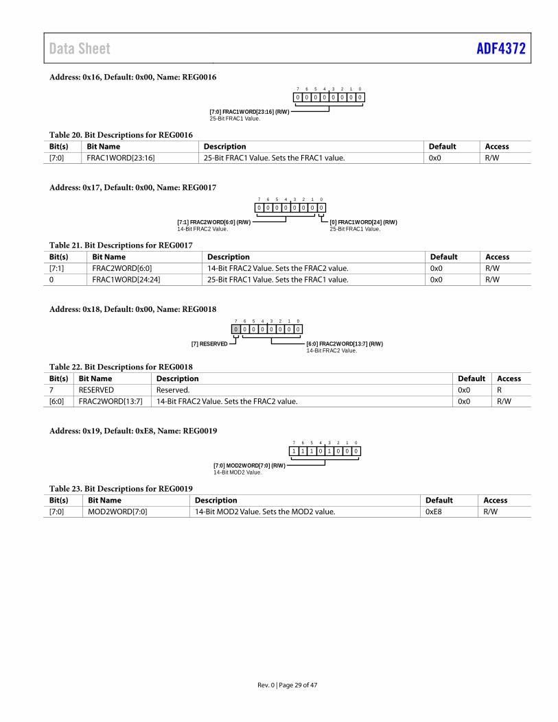
Table 20. Bit Descriptions for REG0016 Bit(s) Bit Name Description Default Access [7:0] FRAC1WORD[23:16] 25-Bit FRAC1 Value. Sets the FRAC1 value. 0x0 R/W
Table 21. Bit Descriptions for REG0017 Bit(s) Bit Name Description Default Access [7:1] FRAC2WORD[6:0] 14-Bit FRAC2 Value. Sets the FRAC2 value. 0x0 R/W 0 FRAC1WORD[24:24] 25-Bit FRAC1 Value. Sets the FRAC1 value. 0x0 R/W
Address: 0x18, Default: 0x00, Name: REG0018
14-Bit FRAC2 Value.
0
01
02
03
04
05
06
07
0
[7] RESERVED [6:0] FRAC2WORD[13:7] (R/W)
Table 22. Bit Descriptions for REG0018 Bit(s) Bit Name Description Default Access 7 RESERVED Reserved. 0x0 R [6:0] FRAC2WORD[13:7] 14-Bit FRAC2 Value. Sets the FRAC2 value. 0x0 R/W
Address: 0x19, Default: 0xE8, Name: REG0019
14-Bit MOD2 Value.
0
01
02
03
14
05
16
17
1
[7:0] MOD2WORD[7:0] (R/W)
Table 23. Bit Descriptions for REG0019 Bit(s) Bit Name Description Default Access [7:0] MOD2WORD[7:0] 14-Bit MOD2 Value. Sets the MOD2 value. 0xE8 R/W
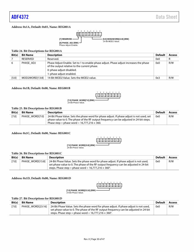
Table 24. Bit Descriptions for REG001A Bit(s) Bit Name Description Default Access 7 RESERVED Reserved. 0x0 R 6 PHASE_ADJ Phase Adjust Enable. Set to 1 to enable phase adjust. Phase adjust increases the phase
of the output relative to the current phase. 0x0 R/W
Table 25. Bit Descriptions for REG001B Bit(s) Bit Name Description Default Access [7:0] PHASE_WORD[7:0] 24-Bit Phase Value. Sets the phase word for phase adjust. If phase adjust is not used, set
phase value to 0. The phase of the RF output frequency can be adjusted in 24-bit steps. Phase step = phase word ÷ 16,777,216 × 360.
0x0 R/W
Address: 0x1C, Default: 0x00, Name: REG001C
24-Bit Phase Value.
0
01
02
03
04
05
06
07
0
[7:0] PHASE_WORD[15:8] (R/W)
Table 26. Bit Descriptions for REG001C Bit(s) Bit Name Description Default Access [7:0] PHASE_WORD[15:8] 24-Bit Phase Value. Sets the phase word for phase adjust. If phase adjust is not used,
set phase value to 0. The phase of the RF output frequency can be adjusted in 24-bit steps. Phase step = phase word ÷ 16,777,216 × 360°.
0x0 R/W
Address: 0x1D, Default: 0x00, Name: REG001D
24-Bit Phase Value.
0
01
02
03
04
05
06
07
0
[7:0] PHASE_WORD[23:16] (R/W)
Table 27. Bit Descriptions for REG001D Bit(s) Bit Name Description Default Access [7:0] PHASE_WORD[23:16] 24-Bit Phase Value. Sets the phase word for phase adjust. If phase adjust is not used,
set phase value to 0. The phase of the RF output frequency can be adjusted in 24-bit steps. Phase step = phase word ÷ 16,777,216 × 360°.
Table 28. Bit Descriptions for REG001E Bit(s) Bit Name Description Default Access [7:4] CP_CURRENT Charge Pump Current Setting. Sets the charge pump current. Set these bits to the charge
pump current that the loop filter is designed for. 0x4 R/W
slope, set phase detector polarity to positive. If using an inverting loop filter and a VCO with a negative tuning slope, set phase detector polarity to positive. If using a noninverting loop filter and a VCO with a negative tuning slope, set phase detector polarity to negative. If using an inverting loop filter and a VCO with a positive tuning slope, set phase detector polarity to negative.
0x1 R/W
0: negative phase detector polarity. 1: positive phase detector polarity. 2 PD Power-Down. Setting to 1 powers down all internal PLL blocks of the ADF4372. The VCO and
multipliers remain powered up. The registers do not lose their values. After bringing the ADF4372 out of power-down (setting to 0) a write to Address 0x10 is required to relock the loop.
0x0 R/W
0: normal operation. 1: power-down. 1 RESERVED Reserved. 0x0 R 0 CNTR_RESET Counter Reset. Setting to 1 holds the N divider and R counter in reset. There are no signals
Table 29. Bit Descriptions for REG001F Bit(s) Bit Name Description Default Access [7:5] RESERVED Reserved. 0x0 R [4:0] R_WORD 5-Bit R Counter. b'00000 corresponds to
divide by 32. 0x1 R/W
Address: 0x20, Default: 0x14, Name: REG0020
Mux Out.
Mux Out Enable.Mux Out Level Select.
0
01
02
13
04
15
06
07
0
[7:4] MUXOUT (R/W) [1:0] RESERVED
[3] MUXOUT_EN (R/W)[2] LEV_SEL (R/W)
Table 30. Bit Descriptions for REG0020 Bit(s) Bit Name Description Default Access [7:4] MUXOUT Mux Out. This bit is used to set the mux out signal when MUXOUT_EN = 1. 0x1 R/W 0: tristate, high impedance output (only works when MUXOUT_EN = 0). 1: digital lock detect. 10: charge pump up. 11: charge pump down. 100: RDIV2. 101: N divider output. 110: VCO test modes. 111: reserved. 1000: high. 1001: VCO calibration R band/2. 1010: VCO calibration N band/2. 3 MUXOUT_EN Mux Out Enable. Set to 0 if using the SDIO pin for register readback. 0x0 R/W 0: data pin used for readback. 1: mux out pin used for readback. 2 LEV_SEL Mux Out Level Select. Select the voltage level of the logic at the mux out. 0x1 R/W 0: 1.8 V logic. 1: 3.3 V logic. [1:0] RESERVED Reserved. 0x0 R
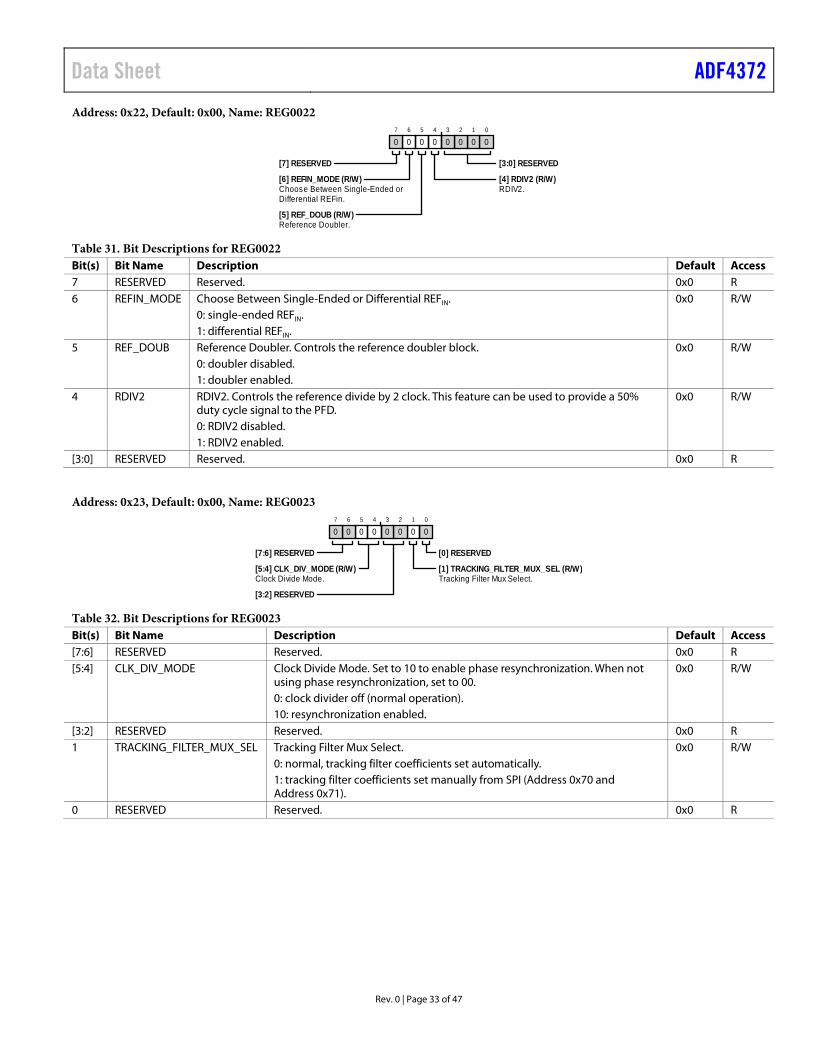
Table 31. Bit Descriptions for REG0022 Bit(s) Bit Name Description Default Access 7 RESERVED Reserved. 0x0 R 6 REFIN_MODE Choose Between Single-Ended or Differential REFIN. 0x0 R/W 0: single-ended REFIN. 1: differential REFIN. 5 REF_DOUB Reference Doubler. Controls the reference doubler block. 0x0 R/W 0: doubler disabled. 1: doubler enabled. 4 RDIV2 RDIV2. Controls the reference divide by 2 clock. This feature can be used to provide a 50%
Table 32. Bit Descriptions for REG0023 Bit(s) Bit Name Description Default Access [7:6] RESERVED Reserved. 0x0 R [5:4] CLK_DIV_MODE Clock Divide Mode. Set to 10 to enable phase resynchronization. When not
using phase resynchronization, set to 00. 0x0 R/W
0: clock divider off (normal operation). 10: resynchronization enabled. [3:2] RESERVED Reserved. 0x0 R 1 TRACKING_FILTER_MUX_SEL Tracking Filter Mux Select. 0x0 R/W 0: normal, tracking filter coefficients set automatically. 1: tracking filter coefficients set manually from SPI (Address 0x70 and
Table 33. Bit Descriptions for REG0024 Bit(s) Bit Name Description Default Access 7 FB_SEL Feedback. 0x1 R/W 0: divider feedback to N counter. 1: fundamental feedback to N counter. [6:4] DIV_SEL Division Selection. 0x0 R/W 0: divide 1. 1: divide 2. 10: divide 4. 11: divide 8. 100: divide 16. 101: divide 32. 110: divide 64. 111: reserved. [3:0] RESERVED Reserved. 0x0 R
Address: 0x25, Default: 0x07, Name: REG0025
Mute to Lock Detect. Select Output Power Level.
RFOUT Enable.
Select if DIV_SEL is Double Buffered.Doubler Path Enable.
Not Used.
0
11
12
13
04
05
06
07
0
[7] MUTE_LD (R/W) [1:0] RF_OUT_POWER (R/W)
[6] RESERVED [2] RF_EN (R/W)
[5] RF_DIVSEL_DB (R/W)[3] X2_EN (R/W)
[4] X4_EN (R/W)
Table 34. Bit Descriptions for REG0025 Bit(s) Bit Name Description Default Access 7 MUTE_LD Mute to Lock Detect. 0x0 R/W 0: mute to lock detect disabled. 1: mute to lock detect enabled, RF output stage gated by digital lock detect asserting
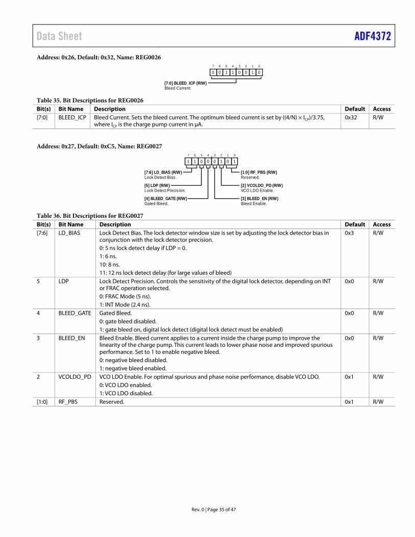
Table 35. Bit Descriptions for REG0026 Bit(s) Bit Name Description Default Access [7:0] BLEED_ICP Bleed Current. Sets the bleed current. The optimum bleed current is set by ((4/N) × ICP)/3.75,
where ICP is the charge pump current in μA. 0x32 R/W
Address: 0x27, Default: 0xC5, Name: REG0027
Lock Detect Bias. Reserved.
Lock Detect Precis ion. VCO LDO Enable.
Gated Bleed. Bleed Enable.
0
11
02
13
04
05
06
17
1
[7:6] LD_BIAS (R/W) [1:0] RF_PBS (R/W)
[5] LDP (R/W) [2] VCOLDO_PD (R/W)
[4] BLEED_GATE (R/W) [3] BLEED_EN (R/W)
Table 36. Bit Descriptions for REG0027 Bit(s) Bit Name Description Default Access [7:6] LD_BIAS Lock Detect Bias. The lock detector window size is set by adjusting the lock detector bias in
conjunction with the lock detector precision. 0x3 R/W
0: 5 ns lock detect delay if LDP = 0. 1: 6 ns. 10: 8 ns. 11: 12 ns lock detect delay (for large values of bleed) 5 LDP Lock Detect Precision. Controls the sensitivity of the digital lock detector, depending on INT
or FRAC operation selected. 0x0 R/W
0: FRAC Mode (5 ns). 1: INT Mode (2.4 ns). 4 BLEED_GATE Gated Bleed. 0x0 R/W 0: gate bleed disabled. 1: gate bleed on, digital lock detect (digital lock detect must be enabled) 3 BLEED_EN Bleed Enable. Bleed current applies to a current inside the charge pump to improve the
linearity of the charge pump. This current leads to lower phase noise and improved spurious performance. Set to 1 to enable negative bleed.
Table 37. Bit Descriptions for REG0028 Bits Bit Name Description Reset Access [7:3] RESERVED Reserved. 0x0 R [2:1] LD_COUNT Lock Detector Count. Initial value of the lock detector. This field sets the number of counts of PFD
within lock window before asserting digital lock detect high. 0x1 R/W
0: 1024 cycles. 1: 2048 cycles. 10: 4096 cycles. 11: 8192 cycles. 0 LOL_EN Loss of Lock Enable. When loss of lock is enabled, if digital lock detect is asserted, and the
reference signal is removed, digital lock detect goes low. It is recommended to set this bit to 1 to enable loss of lock.
0x1 R/W
0: loss of lock disabled 1: loss of lock enabled.
Address: 0x2A, Default: 0x00, Name: REG002A
Readback Select.
Bleed Polarity.
CSB from Pin, Synchronized withREFN
0
01
02
03
04
05
06
07
0
[7:6] RESERVED [0] READ_SEL (R/W)
[5] BLEED_POL (R/W)[2:1] RESERVED
[4] RESERVED [3] LE_SEL (R/W)
Table 38. Bit Descriptions for REG002A Bit(s) Bit Name Description Default Access [7:6] RESERVED Reserved. 0x0 R 5 BLEED_POL Bleed Polarity. Controls the polarity of the bleed current. Negative is typical usage. 0x0 R/W 0: negative bleed. 1: positive bleed (not recommended). 4 RESERVED Reserved. 0x0 R 3 LE_SEL CS from Pin, Synchronized with REFN. 0x0 R/W
0: CS synchronization disabled.
1: CS synchronization enabled.
[2:1] RESERVED Reserved. 0x0 R 0 READ_SEL Readback Select. Selects the value to be read back. 0x0 R/W 0: readback VCO, band, and bias compensation data. 1: readback device version ID.
Adds 1/2 bit to FRAC1 when auxiliarySDM is off (VAR_MOD_EN=0) .
Enable Auxiliary SDM.Mask ΣΔ Reset when REG0010 isupdated.
0
11
02
03
04
05
06
07
0
[7:6] RESERVED [0] SD_EN_FRAC0 (R/W)
[5] LSB_P1 (R/W)[1] RESERVED
[4] VAR_MOD_EN (R/W)[2] SD_LOAD_ENB (R/W)
[3] RESERVED
Table 39. Bit Descriptions for REG002B Bit(s) Bit Name Description Default Access [7:6] RESERVED Reserved. 0x0 R 5 LSB_P1 Adds a half bit to FRAC1 when auxiliary SDM is off (VAR_MOD_EN = 0). Set to 0 for normal
operation. 0x0 R/W
4 VAR_MOD_EN Enable Auxiliary SDM. If FRAC2 is different than 0, this bit is programmed to 1. 0x1 R/W 0: normal operation. 1: enable auxiliary SDM. 3 RESERVED Reserved. 0x0 R 2 SD_LOAD_ENB Mask Σ-Δ Reset when Address 0x10 is Updated. 0x0 R/W 1 RESERVED Reserved. 0x0 R 0 SD_EN_FRAC0 Σ-Δ Enable. Set to 1 when in integer mode (when FRAC1 = FRAC2 = 0), and set to 0 when in
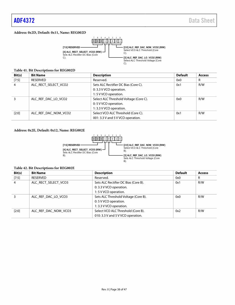
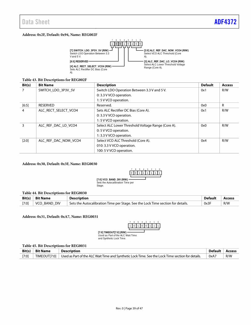
Table 43. Bit Descriptions for REG002F Bit(s) Bit Name Description Default Access 7 SWITCH_LDO_3P3V_5V Switch LDO Operation Between 3.3 V and 5 V. 0x1 R/W 0: 3.3 V VCO operation. 1: 5 V VCO operation. [6:5] RESERVED Reserved. 0x0 R 4 ALC_RECT_SELECT_VCO4 Sets ALC Rectifier DC Bias (Core A). 0x1 R/W 0: 3.3 V VCO operation. 1: 5 V VCO operation. 3 ALC_REF_DAC_LO_VCO4 Select ALC Lower Threshold Voltage Range (Core A). 0x0 R/W 0: 5 V VCO operation. 1: 3.3 V VCO operation. [2:0] ALC_REF_DAC_NOM_VCO4 Select VCO ALC Threshold (Core A). 0x4 R/W 010: 3.3 V VCO operation. 100: 5 V VCO operation.
Address: 0x30, Default: 0x3F, Name: REG0030
Sets the Autocalibration Time perStage.
0
11
12
13
14
15
16
07
0
[7:0] VCO_BAND_DIV (R/W)
Table 44. Bit Descriptions for REG0030 Bit(s) Bit Name Description Default Access [7:0] VCO_BAND_DIV Sets the Autocalibration Time per Stage. See the Lock Time section for details. 0x3F R/W
Address: 0x31, Default: 0xA7, Name: REG0031
Used as Part of the ALC Wait Timeand Synthetic Lock Time.
0
11
12
13
04
05
16
07
1
[7:0] TIMEOUT[7:0] (R/W)
Table 45. Bit Descriptions for REG0031 Bit(s) Bit Name Description Default Access [7:0] TIMEOUT[7:0] Used as Part of the ALC Wait Time and Synthetic Lock Time. See the Lock Time section for details. 0xA7 R/W
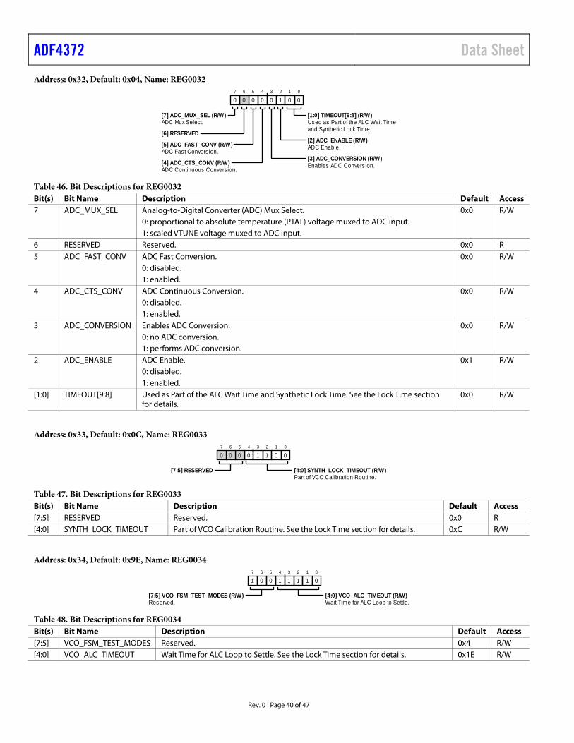
Table 46. Bit Descriptions for REG0032 Bit(s) Bit Name Description Default Access 7 ADC_MUX_SEL Analog-to-Digital Converter (ADC) Mux Select. 0x0 R/W 0: proportional to absolute temperature (PTAT) voltage muxed to ADC input. 1: scaled VTUNE voltage muxed to ADC input. 6 RESERVED Reserved. 0x0 R 5 ADC_FAST_CONV ADC Fast Conversion. 0x0 R/W 0: disabled. 1: enabled. 4 ADC_CTS_CONV ADC Continuous Conversion. 0x0 R/W 0: disabled. 1: enabled. 3 ADC_CONVERSION Enables ADC Conversion. 0x0 R/W 0: no ADC conversion. 1: performs ADC conversion. 2 ADC_ENABLE ADC Enable. 0x1 R/W 0: disabled. 1: enabled. [1:0] TIMEOUT[9:8] Used as Part of the ALC Wait Time and Synthetic Lock Time. See the Lock Time section
for details. 0x0 R/W
Address: 0x33, Default: 0x0C, Name: REG0033
Part of VCO Calibration Routine.
0
01
02
13
14
05
06
07
0
[7:5] RESERVED [4:0] SYNTH_LOCK_TIMEOUT (R/W)
Table 47. Bit Descriptions for REG0033 Bit(s) Bit Name Description Default Access [7:5] RESERVED Reserved. 0x0 R [4:0] SYNTH_LOCK_TIMEOUT Part of VCO Calibration Routine. See the Lock Time section for details. 0xC R/W
Table 48. Bit Descriptions for REG0034 Bit(s) Bit Name Description Default Access [7:5] VCO_FSM_TEST_MODES Reserved. 0x4 R/W [4:0] VCO_ALC_TIMEOUT Wait Time for ALC Loop to Settle. See the Lock Time section for details. 0x1E R/W
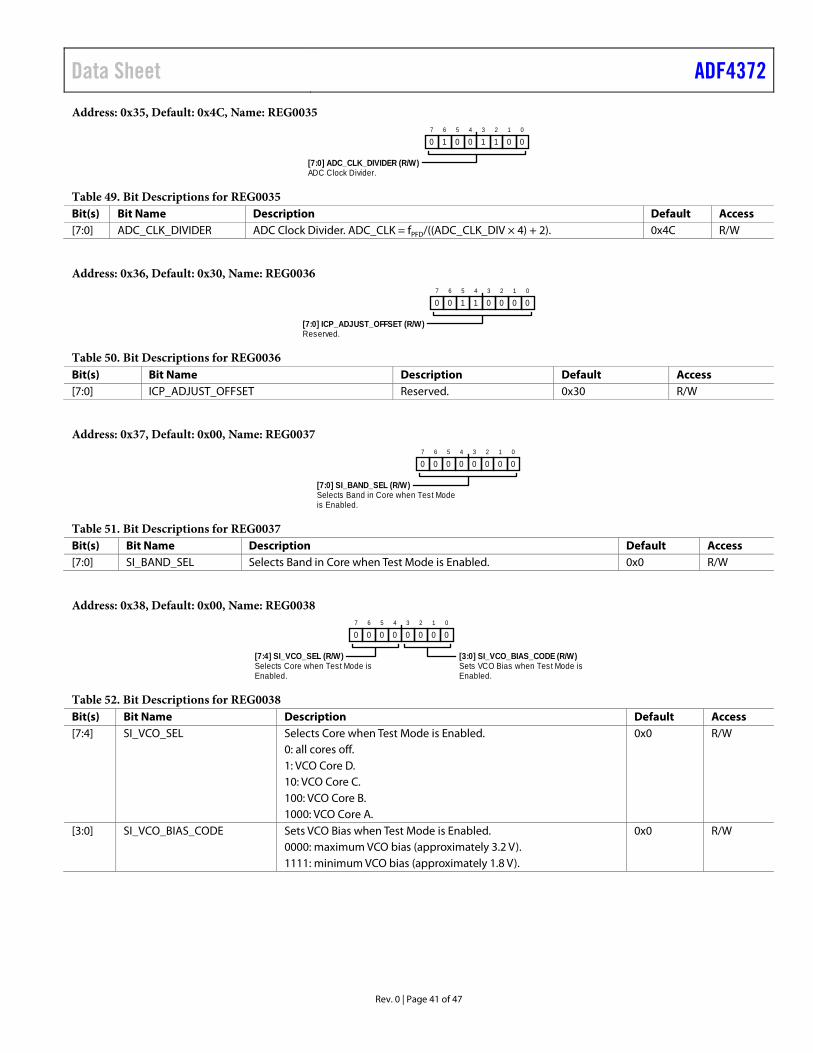
Table 49. Bit Descriptions for REG0035 Bit(s) Bit Name Description Default Access [7:0] ADC_CLK_DIVIDER ADC Clock Divider. ADC_CLK = fPFD/((ADC_CLK_DIV × 4) + 2). 0x4C R/W
Address: 0x36, Default: 0x30, Name: REG0036
Reserved.
0
01
02
03
04
15
16
07
0
[7:0] ICP_ADJUST_OFFSET (R/W)
Table 50. Bit Descriptions for REG0036 Bit(s) Bit Name Description Default Access [7:0] ICP_ADJUST_OFFSET Reserved. 0x30 R/W
Address: 0x37, Default: 0x00, Name: REG0037
Selects Band in Core when Test Modeis Enabled.
0
01
02
03
04
05
06
07
0
[7:0] SI_BAND_SEL (R/W)
Table 51. Bit Descriptions for REG0037 Bit(s) Bit Name Description Default Access [7:0] SI_BAND_SEL Selects Band in Core when Test Mode is Enabled. 0x0 R/W
Table 52. Bit Descriptions for REG0038 Bit(s) Bit Name Description Default Access [7:4] SI_VCO_SEL Selects Core when Test Mode is Enabled. 0x0 R/W 0: all cores off. 1: VCO Core D. 10: VCO Core C. 100: VCO Core B. 1000: VCO Core A. [3:0] SI_VCO_BIAS_CODE Sets VCO Bias when Test Mode is Enabled. 0x0 R/W 0000: maximum VCO bias (approximately 3.2 V). 1111: minimum VCO bias (approximately 1.8 V).
Select VCO VTUNE Target Voltagewhen Test Mode is Enabled.
VCO Test Mux Select.
0
11
12
13
04
05
06
07
0
[7] RESERVED [3:0] SI_VTUNE_CAL_SET (R/W)
[6:4] VCO_FSM_TEST_MUX_SEL (R/W)
Table 53. Bit Descriptions for REG0039 Bit(s) Bit Name Description Default Access 7 RESERVED Reserved. 0x0 R [6:4] VCO_FSM_TEST_MUX_SEL VCO Test Mux Select. 0x0 R/W 0: busy. 1: N band. 10: R band. 11: reserved. 100: timeout clock. 101: bias minimum. 110: ADC busy. 111: logic low. [3:0] SI_VTUNE_CAL_SET Select VCO VTUNE Target Voltage when Test Mode is Enabled. 0x7 R/W 0: 0.58 V. 1: 0.73 V. 10: 0.88 V. 11: 1.03 V. 100: 1.18 V. 101: 1.33 V. 110: 1.48 V. 111: 1.63 V. 1000: 1.78 V. 1001: 1.93 V. 1010: 2.08 V. 1011: 2.23 V. 1100: 2.38 V. 1101: 2.53 V. 1110: 2.68 V. 1111: 2.83 V.
Address: 0x3A, Default: 0x55, Name: REG003A
VCO Calibration ADC Offset Correction.
0
11
02
13
04
15
06
17
0
[7:0] ADC_OFFSET (R/W)
Table 54. Bit Descriptions for REG003A Bit(s) Bit Name Description Default Access [7:0] ADC_OFFSET VCO Calibration ADC Offset Correction. 0x55 R/W
Table 55. Bit Descriptions for REG003D Bit(s) Bit Name Description Default Access 7 RESERVED Reserved. 0x0 R 6 SD_RESET Reserved. 0x0 R/W [5:0] RESERVED Reserved. 0x0 R
Address: 0x3E, Default: 0x0C, Name: REG003E
Charge Pump Test Modes.
0
01
02
13
14
05
06
07
0
[7:4] RESERVED [1:0] RESERVED
[3:2] CP_TMODE (R/W)
Table 56. Bit Descriptions for REG003E Bit(s) Bit Name Description Default Access [7:4] RESERVED Reserved. 0x0 R [3:2] CP_TMODE CP Test Modes 0x3 R/W 0: CP tristate 11: normal operation [1:0] RESERVED Reserved. 0x0 R
Address: 0x3F, Default: 0x80, Name: REG003F
Reserved.
0
01
02
03
04
05
06
07
1
[7:0] CLK1_DIV[7:0] (R/W)
Table 57. Bit Descriptions for REG003F Bit(s) Bit Name Description Default Access [7:0] CLK1_DIV[7:0] Reserved. 0x80 R/W
Address: 0x40, Default: 0x50, Name: REG0040
Reserved.
Reserved.
0
01
02
03
04
15
06
17
0
[7] RESERVED [3:0] CLK1_DIV[11:8] (R/W)
[6:4] TRM_IB_VCO_BUF (R/W)
Table 58. Bit Descriptions for REG0040 Bit(s) Bit Name Description Default Access 7 RESERVED Reserved. 0x0 R [6:4] TRM_IB_VCO_BUF Reserved. 0x5 R/W [3:0] CLK1_DIV[11:8] Reserved. 0x0 R/W
Table 59. Bit Descriptions for REG0041 Bit(s) Bit Name Description Default Access [7:0] CLK2_DIVIDER_1[7:0] Reserved. 0x28 R/W
Address: 0x47, Default: 0xC0, Name: REG0047
Reserved.
0
01
02
03
04
05
06
17
1
[7:5] TRM_RESD_VCO_MUX (R/W) [4:0] RESERVED
Table 60. Bit Descriptions for REG0047 Bit(s) Bit Name Description Default Access [7:5] TRM_RESD_VCO_MUX Reserved. 0x6 R/W [4:0] RESERVED Reserved. 0x0 R
Address: 0x52, Default: 0xF4, Name: REG0052
Reserved.
Reserved.
0
01
02
13
04
15
16
17
1
[7:5] TRM_RESD_VCO_BUF (R/W) [1:0] RESERVED
[4:2] TRM_RESCI_VCO_BUF (R/W)
Table 61. Bit Descriptions for REG0052 Bit(s) Bit Name Description Default Access [7:5] TRM_RESD_VCO_BUF Reserved. VCO buffer trim. 0x7 R/W [4:2] TRM_RESCI_VCO_BUF Reserved. 0x5 R/W [1:0] RESERVED Reserved. 0x0 R
Address: 0x6E, Default: 0x00, Name: REG006E
Open-Loop VCO Counter Readback.
0
01
02
03
04
05
06
07
0
[7:0] VCO_DATA_READBACK[7:0] (R)
Table 62. Bit Descriptions for REG006E Bit(s) Bit Name Description Default Access [7:0] VCO_DATA_READBACK[7:0] Open-Loop VCO Counter Readback. 0x0 R
Address: 0x6F, Default: 0x00, Name: REG006F
Open-Loop VCO Counter Readback.
0
01
02
03
04
05
06
07
0
[7:0] VCO_DATA_READBACK[15:8] (R)
Table 63. Bit Descriptions for REG006F Bit(s) Bit Name Description Default Access [7:0] VCO_DATA_READBACK[15:8] Open-Loop VCO Counter Readback. 0x0 R
Table 64. Bit Descriptions for REG0070 Bit(s) Bit Name Description Default Access [7:5] BAND_SEL_X2 Filter Select for Doubler Output
Tracking Filter. 0x0 R/W
[4:2] RESERVED Reserved. 0x0 R [1:0] BIAS_SEL_X2 Bias Select for Doubler Output
Tracking Bias. 0x3 R/W
Address: 0x71, Default: 0x60, Name: REG0071
Not Used. Not Used.
0
01
02
03
04
05
16
17
0
[7:5] BAND_SEL_X4 (R/W) [1:0] BIAS_SEL_X4 (R/W)
[4:2] RESERVED
Table 65. Bit Descriptions for REG0071 Bit(s) Bit Name Description Default Access [7:5] BAND_SEL_X4 Not Used. 0x3 R/W [4:2] RESERVED Reserved. 0x0 R [1:0] BIAS_SEL_X4 Not Used. 0x0 R/W
Address: 0x72, Default: 0x32, Name: REG0072
Auxillary RF Output Frequency Select. Reserved.
Auxiliary RF Output Power.
Power-Down Auxiliary RF Output.
0
01
12
03
04
15
16
07
0
[7] RESERVED [0] RESERVED
[6] AUX_FREQ_SEL (R/W) [1] COUPLED_VCO (R/W)
[5:4] POUT_AUX (R/W) [2] RESERVED
[3] PDB_AUX (R/W)
Table 66. Bit Descriptions for REG0072 Bit(s) Bit Name Description Default Access 7 RESERVED Reserved. 0x0 R 6 AUX_FREQ_SEL Auxiliary RF Output Frequency Select. 0x0 R/W 0: divided output. 1: VCO output. [5:4] POUT_AUX Auxiliary RF Output Power. Sets the output power at the auxiliary RF output ports. 0x3 R/W 0: −4.5 dBm single-ended ÷ −1.5 dBm differential. 1: 1 dBm single-ended ÷ 4 dBm differential. 10: 4 dBm single-ended ÷ 7 dBm differential. 11: 6 dBm single-ended ÷ 9 dBm differential. 3 PDB_AUX Power-Down Auxiliary RF Output. 0x0 R/W 0: auxiliary RF off. 1: auxiliary RF on. 2 RESERVED Reserved. 0x0 R 1 COUPLED_VCO Reserved. 0x1 R/W 0 RESERVED Reserved. 0x0 R
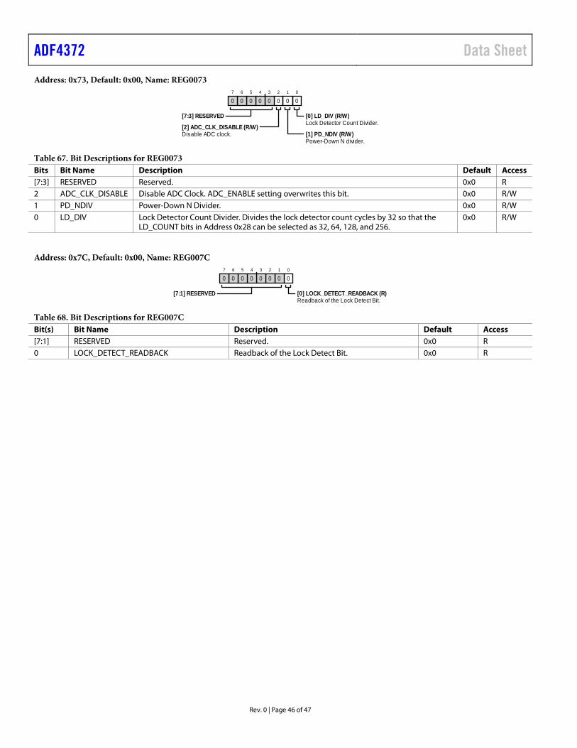
Table 67. Bit Descriptions for REG0073 Bits Bit Name Description Default Access [7:3] RESERVED Reserved. 0x0 R 2 ADC_CLK_DISABLE Disable ADC Clock. ADC_ENABLE setting overwrites this bit. 0x0 R/W 1 PD_NDIV Power-Down N Divider. 0x0 R/W 0 LD_DIV Lock Detector Count Divider. Divides the lock detector count cycles by 32 so that the
LD_COUNT bits in Address 0x28 can be selected as 32, 64, 128, and 256. 0x0 R/W
Address: 0x7C, Default: 0x00, Name: REG007C
Readback of the Lock Detect Bit.
0
01
02
03
04
05
06
07
0
[7:1] RESERVED [0] LOCK_DETECT_READBACK (R)
Table 68. Bit Descriptions for REG007C Bit(s) Bit Name Description Default Access [7:1] RESERVED Reserved. 0x0 R 0 LOCK_DETECT_READBACK Readback of the Lock Detect Bit. 0x0 R