291
| Date post: | 18-Nov-2014 |
| Category: |
Documents |
| Upload: | api-19915961 |
| View: | 842 times |
| Download: | 8 times |


Millimetre WaveAntennas forGigabit WirelessCommunicationsA Practical Guide to Design andAnalysis in a System Context
Kao-Cheng Huang
University of Greenwich, UK
David J. Edwards
University of Oxford, UK
A John Wiley and Sons, Ltd, Publication

Millimetre Wave Antennasfor Gigabit WirelessCommunications


Millimetre WaveAntennas forGigabit WirelessCommunicationsA Practical Guide to Design andAnalysis in a System Context
Kao-Cheng Huang
University of Greenwich, UK
David J. Edwards
University of Oxford, UK
A John Wiley and Sons, Ltd, Publication

This edition first published 2008© 2008 John Wiley & Sons Ltd
Registered officeJohn Wiley & Sons Ltd, The Atrium, Southern Gate, Chichester, West Sussex, PO19 8SQ, United Kingdom
For details of our global editorial offices, for customer services and for information about how to apply forpermission to reuse the copyright material in this book please see our website at www.wiley.com.
The right of the author to be identified as the author of this work has been asserted in accordancewith the Copyright, Designs and Patents Act 1988.
All rights reserved. No part of this publication may be reproduced, stored in a retrieval system, or transmitted,in any form or by any means, electronic, mechanical, photocopying, recording or otherwise, except as permittedby the UK Copyright, Designs and Patents Act 1988, without the prior permission of the publisher.
Wiley also publishes its books in a variety of electronic formats. Some content that appears in printmay not be available in electronic books.
Designations used by companies to distinguish their products are often claimed as trademarks. All brand namesand product names used in this book are trade names, service marks, trademarks or registered trademarks oftheir respective owners. The publisher is not associated with any product or vendor mentioned in this book.This publication is designed to provide accurate and authoritative information in regard to the subject mattercovered. It is sold on the understanding that the publisher is not engaged in rendering professional services.If professional advice or other expert assistance is required, the services of a competent professional shouldbe sought.
Library of Congress Cataloging-in-Publication Data
Huang, Kao-Cheng.Millimetre wave antennas for gigabit wireless communications : a practical guideto design and analysis in a system context / Kao-Cheng Huang, David J. Edwards.
p. cm.Includes bibliographical references and index.ISBN 978-0-470-51598-3 (cloth)1. Microwave antennas. 2. Gigabit communications. 3. Milimeter waves.I. Edwards, David J. II. Title.TK7871.67.M53H83 2008621.382′4—dc22
2008013165
A catalogue record for this book is available from the British Library
ISBN 978-0-470-51598-3 (HB)
Set in 10/12pt Times by Integra Software Services Pvt. Ltd, Pondicherry, IndiaPrinted in Singapore by Markono Print Media Pte Ltd, Singapore.

Contents
Preface ix
List of Abbreviations xi
1 Gigabit Wireless Communications 11.1 Gigabit Wireless Communications 11.2 Regulatory Issues 7
1.2.1 Europe 71.2.2 United States 81.2.3 Japan 91.2.4 Industrial Standardisation 9
1.3 Millimetre Wave Characterisations 121.3.1 Free Space Propagation 131.3.2 Millimetre Wave Propagation Loss Factors 131.3.3 Atmospheric Losses 14
1.4 Channel Performance 141.5 System Design and Performance 22
1.5.1 Antenna Arrays 221.5.2 Transceiver Architecture 23
1.6 Antenna Requirements 261.7 Link Budget 301.8 Summary 34References 34
2 Critical Antenna Parameters 372.1 Path Loss and Antenna Directivity 382.2 Antenna Beamwidth 452.3 Maximum Possible Gain-to-Q 462.4 Antenna Polarisation 50
2.4.1 Polarisation Diversity 56References 58
3 Planar Antennas 613.1 Printed Antennas 613.2 Slot Antennas 72
3.2.1 Standard Slot Antenna 723.2.2 Tapered Slot Antennas 73

vi CONTENTS
3.3 Quasi-Yagi Antennas 753.4 Bow-Tie Antennas 763.5 Reflector Antennas 783.6 Millimetre Wave Design Considerations 843.7 Production and Manufacture 85
3.7.1 Fine Line Printing 853.7.2 Thick Film 863.7.3 Thin Film 863.7.4 System-on-Chip 87
References 87
4 Horn Antennas 914.1 Waveguide Modes 914.2 Multimode Horn Antennas 944.3 Integrated Horn 984.4 Conical Horns and Circular Polarisation 1024.5 Tilt Horn 1104.6 Dielectric Sectoral Horn 111References 112
5 Dielectric Antennas 1155.1 Dielectric Resonator Antennas 1155.2 Dielectric Rod Antennas 1215.3 Maximum Gain Rod Antennas 1265.4 The Dual Rod Antenna 1275.5 Patch-Fed Circular Rod Antennas 1305.6 Rod Arrays and Phase Compensation 1365.7 Optimisation of a Rod Antenna 139References 141
6 Lens Antennas 1456.1 Luneberg Lens 1466.2 Hemispherical Lens 1496.3 Extended Hemispherical Lens 1516.4 Off-Axis Extended Hemispherical Lens 1576.5 Planar Lens Array 1616.6 Metal Plate Lens Antennas 164References 166
7 Multiple Antennas 1717.1 The 60 GHz Multibeam Antenna 1717.2 Antenna Arrays 1767.3 Millimetre Wave Arrays 180
7.3.1 Printed Arrays 1807.3.2 Waveguide Arrays 1827.3.3 Leaky-Wave Arrays 184
7.4 Mutual Coupling between Antennas 186References 194

CONTENTS vii
8 Smart Antennas 1978.1 Beam-Switching Antennas 1998.2 Beam-Steering/Forming Antennas 205
8.2.1 Electronic Beamforming 2068.3 Millimetre Wave MIMO 212
8.3.1 Beamforming Layer 2158.3.2 Spatial Multiplexing Layer 217
8.4 Mode-Tracking Antennas 218References 224
9 Advanced Antenna Materials 2279.1 Low-Temperature Co-fired Ceramics 2289.2 Liquid Crystal Polymer 2339.3 CMOS 2389.4 Meta Materials 2419.5 High-Temperature Superconducting Antenna 2459.6 Nano Antennas 249References 249
10 High-Speed Wireless Applications 25510.1 V-Band Antenna Applications 255
10.1.1 Wireless Personal Area Networks (WPANs) 25610.1.2 Wireless HDMI 25610.1.3 Point-to-Point 60 GHz Links 25710.1.4 Broadcasting a Video Signal Transmission System in a Sports Stadium 25710.1.5 Intervehicle Communication System 25810.1.6 Multigigabit File Transmission 25810.1.7 Current Developments 258
10.2 E-Band Antenna Applications 26110.2.1 Private Networks/Enterprise LAN Extensions 26110.2.2 Fibre Extensions 26210.2.3 Fibre Back-up/Diversity Connections 26210.2.4 Military Communications and Surveillance Systems 26210.2.5 Secure Applications 263
10.3 Distributed Antenna Systems 26410.4 Wireless Mesh Networks 267References 270
Index 273

Preface
This book presents antenna design and analysis at the level to produce an understanding ofthe interaction between a wireless system and its antenna, so that the overall performance canbe predicted. Gigabit wireless communications require a considerable amount of bandwidth,which can be supported by millimetre waves. Millimetre wave technology has now come ofage, and at the time of writing the standards of IEEE 802.15.3c, WirelessHDTM and ECMA areon schedule to be finalised. The technology has attracted new commercial wireless applicationsand new markets, such as the capacity for high-speed downloading and wireless high-definitionTVs. This book summarises and reports the extensive research over recent years and emphas-ises the importance and requirements of antennas for gigabit wireless communications, withan emphasis on wireless communications in the 60 GHz ISM band and in the E-band. Thisbook I reviews the particular requirements for this application and addresses the design andfeasibility of millimetre wave antennas; such as planar antennas, rod antennas and antennaarrays. Examples of designs are included, along with a detailed analysis of their performance.In addition, this book includes a bibliography of current research literature and patents in thissubject area. Finally, the applications of these antennas are discussed in the light of differentforthcoming wireless standards.
Millimetre Wave Antennas for Gigabit Wireless Communications endeavours to offer acomprehensive treatment of antennas based on electronic consumer applications, providinga link to applications of computer-aided design tools and advanced materials and technolo-gies. The major features of this book include a discussion of the many novel millimetre waveantenna configurations available with newly reported design techniques and methods.
Although it contains some introductory material, this book is intended to provide a collectionof millimetre wave antenna design considerations for communication system designers andantenna designers. The book should also act as a reference for postgraduate students, research-ers and engineers in millimetre wave engineering and an introduction to the various designconsiderations. It can also be used for millimetre wave teaching. A summary of each chapteris given below.
Chapter 1 introduces the near-term developments in millimetre wave communications. Theimportance and requirements of millimetre wave antennas are discussed based on channelperformance, link budget, and applications in line-of-sight and non-line-of-sight scenarios.Sections addressing system-level considerations include references to subsequent chaptersthat contain a more detailed treatment of antenna design.
Chapters 2 to 8 address conventional configurations of millimetre wave antennas.Chapter 2 considers several critical factors that limit the performance of millimetre wave
antennas.As the antenna design has become critical in wireless communications, the limitationsof antenna design are also discussed in this chapter.
x PREFACE
Chapter 3 describes the variety of millimetre wave planar antennas, and lists basic feedingmethods and useful references on a wide variety of techniques for producing low-profileantennas.
Chapter 4 deals with millimetre wave integrated horn antennas. The chapter includes adiscussion of circular polarisation optimisation techniques, such as those for array antennas.With circular waveguide modes that can be used for mode tracking described in Chapter 8.
Chapter 5 addresses low cost and high directivity of millimetre wave rod antennas. Differentfeeding methods, maximum gain, and beam tilting are discussed in detail. With multiple-rodantennas that can be used as beam-switching antennas discussed in Chapter 7.
Chapter 6 describes the variety of millimetre wave lens antennas, relevant feeding methodsand novel architectures. Lens antennas, with the advantages of light weight and small height,are identified as designs that can be used for new applications.
Chapter 7 discusses millimetre wave multibeam antennas and their construction. Novelantennas with advanced radiation characteristics have been demonstrated. Some of the effectsof mutual coupling of signals and noises between array elements are covered. This interactionmodifies the active array element patterns and can cause impedance changes during scanning.
Chapter 8 focuses on smart antennas and their usage in wireless communications. Wide-ranging technologies such as beam switching, beam steering, MIMO and mode tracking, thatsatisfy special needs are considered. These technologies could produce low-profile high-gain electronic scanning systems in conjunction with the antenna elements described inChapters 3 to 7.
Chapter 9 explores millimetre wave antenna materials and manufacturing techniques.Materials technologies are discussed such as LTCC, LCP, CMOS, high-temperature super-conductors, carbon nanotubes, etc. New materials offer new design concepts and promisefuture exciting antenna technology trends.
Finally, chapter 10, extrapolates the wireless applications of millimetre wave antennas ina envisaged future market. This book only briefly addresses the details of electromagneticanalysis, with the fundamentals of the subject requiring a more detailed study than can begiven in this system design-oriented book.
First of all, the authors wish to acknowledge the copyright permission from IEEE (US),European Microwave Association (Belgium), John Wiley & Sons, Inc. (US), ERA (UK) andSu Khiong Yong (US).
The authors are indebted to many researchers for their published works, which were richsources of reference upon which this book reports and summarises. Their sincere gratitudeextends to the Editor, Sarah Hinton, and the reviewers for their support in the writing of thisbook. The help provided by Tiina Ruonamaa and other members of the staff at John Wiley &Sons, Ltd is most appreciated. The authors also wish to thank their colleagues at the Universityof Oxford, and University of Greenwich.
In addition, Kao-Cheng Huang would like to thank Prof. Mook-Seng Leong, NationalUniversity of Singapore (Singapore), Prof. Rüdiger Vahldieck, ETH (Switzerland),Prof. Ban-Leong Ooi, National University of Singapore (Singapore), Dr David Haigh, ImperialCollege (UK), Prof. Francis Lau, Hong Kong Polytechnic University (China), Dr H.M. Shen,University of Edinburgh (UK), Dr Chris Stevens, University of Oxford (UK) and Dr Jia-ShengHong, Heriot-Watt University (UK) for their many years of support. David Edwards wouldalso like to thank Charlotte Edwards for her help in the final stages of the book. Note: Duringthe later stages of the production of this book Dr Kao-Cheng Huang was taken seriously ill.The book has been completed from his notes and we apologise for any resulting omissions.

List of Abbreviations
A/V audio/visualADC analogue-to-digital conversionAP access pointsAR axial ratioARIB Association of Radio Industries and BusinessASP aperture stacked patchBER bit error rateCB-FGC conductor-backed finite ground coplanarCBCPW conductor-backed coplanar waveguideCCS complementary conducting stripCEPT European Conference of Postal and Telecommunications AdministrationsCPS coplanar striplineCTE coefficient of thermal expansionDAS distributed antenna systemsDBF digital beamformingDLA discrete lens arrayDoA direction of arrivalDRA dielectric resonator antennaEBGs electromagnetic bandgapsECC Electronic Communications CommitteeECMA European Computer Manufacture AssociationEIRP equivalent isotropic radiated powerERC European Radiocommunications CommitteeESPRIT Estimation of Signal Parameters via Rotational Invariance TechniquesETSI European Telecommunications Standards InstituteFCC Federal Communication CommissionsFDA Food and Drug AdministrationFDTD finite-difference time-domainFLA filter–lens arrayFPC Fabry–Perot cavityFT Fourier transformGO geometric opticsGSM Global System for Mobile CommunicationsHDMI high-definition multimedia interface

xii LIST OF ABBREVIATIONS
HDTV high-definition televisionHEM hybrid electromagneticHPBW half-power beamwidthHTS high-temperature superconductorsIC-SMT Industry Canada Spectrum Management and TelecommunicationsISM industrial, scientific and medicalISPs Internet Service ProvidersIVC Inter-Vehicle CommunicationsLA lens arrayLCP liquid crystal polymerLHCP left-hand circular polarisationLHM left-handed materialsLNA low-noise amplifierLOS line-of-sightLPD low probability of detectLPI low probability of interceptLTCC low-temperature co-fired ceramicMANETs mobile ad hoc networksMCM multichip modulesMEMS microelectromechanical systemMIMO multi-input multi-outputMMIC monolithic-microwave integrated circuitMPHPT Ministry of Public Management, Home Affairs, Posts, and TelecommunicationsMSK minimum shift keyingMT mobile terminalNLOS non-line-of-sightOFDM orthogonal frequency division multiplexingOMT orthomode transducerOOK on/off keyingPA 1. power amplifier
2. phased arrayPAPR peak-to-average power ratioPCB printed circuit boardPDA personal data assistantPHY physical layerPMP portable media playerPRS partially reflective surfacePS portable stationPTHs plated through holesQPSK quadrature phase-shift keyingRAUs radio access unitsRF radio frequencyRHCP right-hand circular polarisationRRH remote radio headsSC single carrierSCBT single-carrier block transmission

LIST OF ABBREVIATIONS xiii
SIR signal-to-interferenceSNR signal-to-noise ratioSoC system-on-chipSoP system-on-packageSP3T single-pole triple-throwSSFIP strip slot foam inverted patch antennaULA uniform linear arraysUWB ultra-widebandVCC voltage-controlled oscillatorWLANs wireless local area networksWMN wireless mesh networkWPANs wireless personal area networks

1Gigabit Wireless Communications
The demand for high data rate and high integrity services seems set to grow for the foreseeablefuture. In this chapter the basic ideas and application areas for gigabit Ethernet are introduced,and the requirements for high-performance networks are described. The role of the antenna inthese systems is addressed, and consideration of the performance parameters outlined.
This chapter is organised as follows. Section 1.1 describes a number of applicationscenarios and highlights the requirements for a specific application, namely uncompressedhigh-definition video streaming. Section 1.2 describes the worldwide regulatory effortsand standardisation activities. Section 1.3 presents the characteristics of millimetre waves.Section 1.4 presents measured propagation results and channel performance. Section 1.5describes system design and performance. Section 1.6 discusses the role of the antenna withinthe system and the technical challenges that need to be resolved for the full deployment of60 GHz radio networks. Section 1.7 describes the link budget, which is pivotal in determiningthe performance of the system. In this section noise is also examined, and its impact on linkbehaviour. Section 1.8 summarises the main points of the chapter.
1.1 Gigabit Wireless Communications
The adoption of each successive generation of Ethernet technology has been driven by econom-ics, performance demand, and the rate at which the price of the new generation has approachedthat of the old. As the cost of 100 Mbps Ethernet decreased and approached the previous cost of10 Mbps Ethernet, users rapidly moved to the higher performance standard. In January 2007,10 gigabit Ethernet over copper wiring was announced by the industry [1].Additionally, gigabitEthernet became economic (e.g. below $200) for server connections, and desktop gigabit con-nections have come within $10 or less of the cost of 100 Mbps technology. Consequently,gigabit Ethernet has become the standard for servers, and systems are now routinely orderedwith gigabit Network interface cards. Mirroring events in the wired world, as the prices ofwireless gigabit links approach the prices of 100 Mbps links, users are switching to the higher-performance product, both for traditional wireless applications, as well as for applications thatonly become practical at gigabit speeds.
Millimetre Wave Antennas for Gigabit Wireless Communications Kao-Cheng Huang and David J. Edwardsc© 2008 John Wiley & Sons, Ltd
2 GIGABIT WIRELESS COMMUNICATIONS
In terms of a business model, wireless communications have pointed towards an approach-ing need for gigabit speeds and longer-range connectivity as the applications emerge for homeaudio/visual (A/V) networks, high-quality multimedia, voice and data services. Current wire-less local area networks (WLANs) offer peak rates of 54 Mb/s, with 200–540 Mb/s, such asIEEE 802.11n, becoming available soon. However, even 500 Mb/s is inadequate when facedwith the demand for higher access speed from rich media content and competition from 10 Gb/swired LANs. In addition, future homeA/V networks will require a Gb/s data rate to support mul-tiple high-speed, high-definition A/V streams (e.g. carrying an uncompressed high-definitionvideo at resolutions of up to 1920 × 1080 progressive scans, with latencies ranging from 5 to15 ms) [2].
Based on the technical requirements of applications for high-speed wireless systems, bothindustry and the standardisation bodies need to take into account the following issues:
1. Pressure on data rate increases will persist.2. There is a need for advanced domestic applications such as high-definition wireless
multimedia, which demand higher data rates.3. Data streaming and download/memory back-up times for mobile and personal devices will
also place demands on the shared resource, and user models point to very short dwell timesfor these downloads.
Some approaches, such as IEEE 802.11n, are improving data rates by evolving the exist-ing WLANs standards to increase the data rate; to up to 10 times faster than IEEE 802.11aor 802.11g. Others, such as the ultra-wideband (UWB) are pursuing much more aggressivestrategies, such as sharing spectra with other users.Another approach that will no doubt be takenwill be the time-honoured strategy of moving to higher, unused and unregulated millimetrewave frequencies.
Despite millimetre wave technology having been established for many decades, the mil-limetre wave systems available have mainly been deployed for military applications. Withthe advances in process technologies and low-cost integration solutions, this technology hasstarted to gain a great deal of momentum from academia, industry and standardisation bodies.In very broad terms, millimetre wave technology can be classified as occupying the electro-magnetic spectrum that spans between 30 and 300 GHz, which corresponds to wavelengthsfrom 10 to 1 mm. In this book, the main focus will be on the 60 GHz industrial, scientific andmedical (ISM) band (unless otherwise specified, the terms “60 GHz’’ and “millimetre wave’’will be used interchangeably), which has emerged as one of the most promising candidates formultigigabit wireless indoor communication systems.
Although the IEEE 802.11n standard will improve the robustness of wireless communica-tions, only a modest increase in wireless bandwidth is provided and the data rate is still lowerthan 1 Gb/s. Importantly, 60 GHz technology offers various advantages over currently pro-posed or existing communications systems. One of the deciding factors that makes 60 GHztechnology attractive and has prompted significant interest recently, is the establishment of(relatively) huge unlicensed bandwidths (up to 7 GHz) that are available worldwide. The spec-trum allocations are mainly regulated by the International Telecommunication Union. Thedetails for band allocation around the world can be found in Section 1.2.
While this is comparable to the unlicensed bandwidth allocated for ultra-wideband purposes(∼2–10 GHz), the 60 GHz band is continuous and less restricted in terms of power limits (also
GIGABIT WIRELESS COMMUNICATIONS 3
there are less existing users). This is due to the fact that the UWB system is an overlay sys-tem and thus subject to different considerations and very strict regulation. The large band at60 GHz is in fact one of the largest unlicensed spectral resources allocated in history. This hugebandwidth offers potential in terms of capacity and flexibility and makes 60 GHz technologyparticularly attractive for gigabit wireless applications. Although 60 GHz regulations allowmuch higher transmit power compared to other existing wireless local area networks (e.g. max-imum 100 mW for IEEE 802.11 a/b/g) and wireless personal area network (WPAN) systems, thehigher transmit power is necessary to overcome the higher path loss at 60 GHz (see Table 1.1).
Table 1.1 Path loss and transmit power comparison for differentwireless standards
10 m path loss(dB)
Maximum transmitpower (mW)
802.11a 66 40802.11b/g 60 100802.15.3c 88 500
In addition, the typical 480 Mbps bandwidth of UWB cannot fully support broadcast videoand therefore the data packets need to be recompressed. This forces manufacturers to utiliseexpensive encoders and more memory into their systems, in effect losing video content andadding latency in the process. Therefore, 60 GHz technology could actually provide betterresolution, with less latency and cost for television, DVD players and other high-definitionequipment, compared to UWB.
Taking into consideration the development of consumer electronics, currently the IEEE802.15.3c standard [3] provides 1–3 Gb/s wireless personal area network solutions, projectedfor introduction in the years 2008 to 2009. Also, WiMedia 2.0 [4], which can be used for largefile transfer applications, is to be developed, so the target is to have a data rate of 5 Gb/s orhigher raw bit rates and with more than a 10 m range for indoor applications.
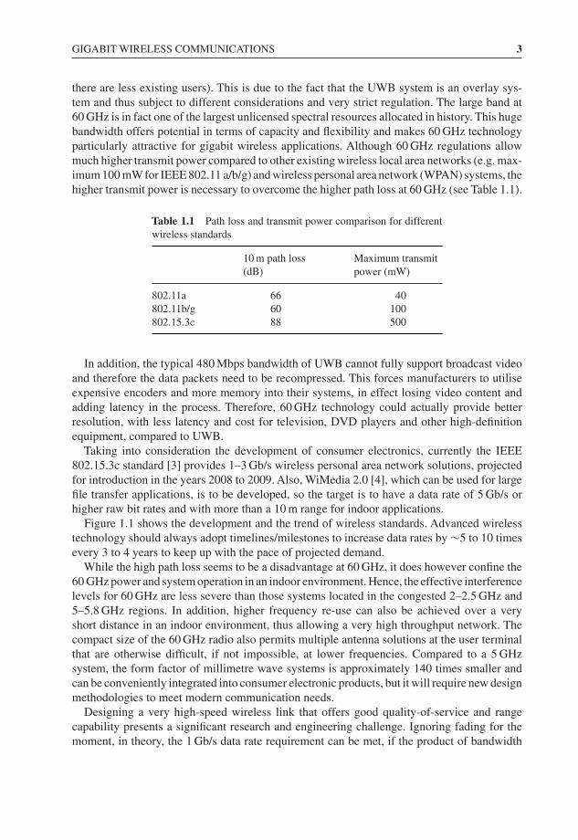
Figure 1.1 shows the development and the trend of wireless standards. Advanced wirelesstechnology should always adopt timelines/milestones to increase data rates by ∼5 to 10 timesevery 3 to 4 years to keep up with the pace of projected demand.
While the high path loss seems to be a disadvantage at 60 GHz, it does however confine the60 GHz power and system operation in an indoor environment. Hence, the effective interferencelevels for 60 GHz are less severe than those systems located in the congested 2–2.5 GHz and5–5.8 GHz regions. In addition, higher frequency re-use can also be achieved over a veryshort distance in an indoor environment, thus allowing a very high throughput network. Thecompact size of the 60 GHz radio also permits multiple antenna solutions at the user terminalthat are otherwise difficult, if not impossible, at lower frequencies. Compared to a 5 GHzsystem, the form factor of millimetre wave systems is approximately 140 times smaller andcan be conveniently integrated into consumer electronic products, but it will require new designmethodologies to meet modern communication needs.
Designing a very high-speed wireless link that offers good quality-of-service and rangecapability presents a significant research and engineering challenge. Ignoring fading for themoment, in theory, the 1 Gb/s data rate requirement can be met, if the product of bandwidth
4 GIGABIT WIRELESS COMMUNICATIONS
WPAN
WLAN
Gen 3: 25-50 Gb/sGen 2: 5-10 Gb/s
802.15.3c
802.11n
802.11a
3.5G3G
2G
802.11b
Cellular/WAN
UWB
19950.01M
0.1M
1M
10M
100M
1G
10G
2000 2005 2010 2015Year
Dat
a R
ate
(bps
)
Figure 1.1 Data rate projections over time [5]
(in units of Hz) and spectral efficiency (in b/s per Hz units) equals 109. As shall be describedin the following sections, a variety of cost, technology and regulatory constraints make sucha solution very challenging.
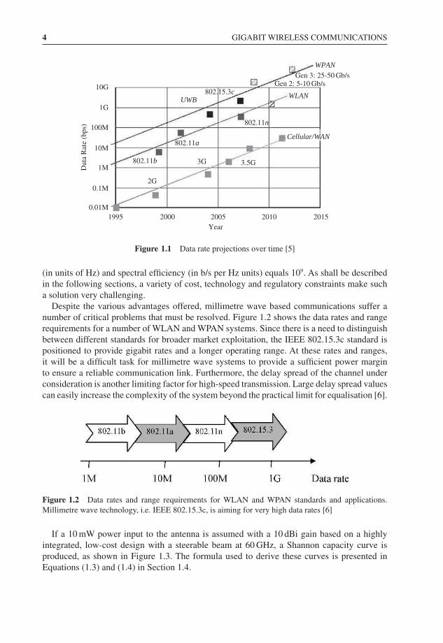
Despite the various advantages offered, millimetre wave based communications suffer anumber of critical problems that must be resolved. Figure 1.2 shows the data rates and rangerequirements for a number of WLAN and WPAN systems. Since there is a need to distinguishbetween different standards for broader market exploitation, the IEEE 802.15.3c standard ispositioned to provide gigabit rates and a longer operating range. At these rates and ranges,it will be a difficult task for millimetre wave systems to provide a sufficient power marginto ensure a reliable communication link. Furthermore, the delay spread of the channel underconsideration is another limiting factor for high-speed transmission. Large delay spread valuescan easily increase the complexity of the system beyond the practical limit for equalisation [6].
Figure 1.2 Data rates and range requirements for WLAN and WPAN standards and applications.Millimetre wave technology, i.e. IEEE 802.15.3c, is aiming for very high data rates [6]
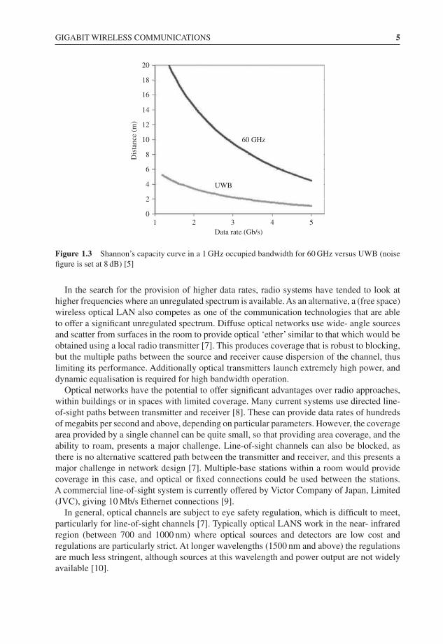
If a 10 mW power input to the antenna is assumed with a 10 dBi gain based on a highlyintegrated, low-cost design with a steerable beam at 60 GHz, a Shannon capacity curve isproduced, as shown in Figure 1.3. The formula used to derive these curves is presented inEquations (1.3) and (1.4) in Section 1.4.
GIGABIT WIRELESS COMMUNICATIONS 5
10
2
4
6
8
10
12
14
16
18
20
2 3 4 5Data rate (Gb/s)
UWB
60 GHzD
ista
nce
(m)
Figure 1.3 Shannon’s capacity curve in a 1 GHz occupied bandwidth for 60 GHz versus UWB (noisefigure is set at 8 dB) [5]
In the search for the provision of higher data rates, radio systems have tended to look athigher frequencies where an unregulated spectrum is available. As an alternative, a (free space)wireless optical LAN also competes as one of the communication technologies that are ableto offer a significant unregulated spectrum. Diffuse optical networks use wide- angle sourcesand scatter from surfaces in the room to provide optical ‘ether’ similar to that which would beobtained using a local radio transmitter [7]. This produces coverage that is robust to blocking,but the multiple paths between the source and receiver cause dispersion of the channel, thuslimiting its performance. Additionally optical transmitters launch extremely high power, anddynamic equalisation is required for high bandwidth operation.
Optical networks have the potential to offer significant advantages over radio approaches,within buildings or in spaces with limited coverage. Many current systems use directed line-of-sight paths between transmitter and receiver [8]. These can provide data rates of hundredsof megabits per second and above, depending on particular parameters. However, the coveragearea provided by a single channel can be quite small, so that providing area coverage, and theability to roam, presents a major challenge. Line-of-sight channels can also be blocked, asthere is no alternative scattered path between the transmitter and receiver, and this presents amajor challenge in network design [7]. Multiple-base stations within a room would providecoverage in this case, and optical or fixed connections could be used between the stations.A commercial line-of-sight system is currently offered by Victor Company of Japan, Limited(JVC), giving 10 Mb/s Ethernet connections [9].
In general, optical channels are subject to eye safety regulation, which is difficult to meet,particularly for line-of-sight channels [7]. Typically optical LANS work in the near- infraredregion (between 700 and 1000 nm) where optical sources and detectors are low cost andregulations are particularly strict. At longer wavelengths (1500 nm and above) the regulationsare much less stringent, although sources at this wavelength and power output are not widelyavailable [10].

6 GIGABIT WIRELESS COMMUNICATIONS
As previously mentioned, the other major problem for optical channels is that of blocking.Line-of-sight channels in particular are required for high-speed operation and these are by theirnature subject to blocking. Within a building, networks must be designed using appropriategeometries to avoid blocking, and this is usually solved by using multiple access points toallow complete coverage [10, 11].
Table 1.2 compares the characteristics of three technologies for gigabit communications:UWB radio, millimetre wave and wireless optics.
Table 1.2 Comparison of three new technologies for gigabit wireless communications [12–14]
Millimetre wave UWB radio Optical wireless
Advantage 1. High data rates (upto Gb/s)
2. Compatible withfibre opticnetworks at60 GHz
1. Low power2. Short range3. Low data4. Penetration through
obstacles in thetransmission path
1. High data rate2. Unlicensed and
unregulated.
Challenge 1. Low cost2. Low power
1. Matched filter problem2. Antenna parameter
trade-off
1. Atmospheric lossranging from10 dB/km(sunny) to350 dB/km(foggy)
2. Multi-user application3. No protection for the
link
Peer-to-peer Indoor/outdoor Indoor/outdoor Indoor/outdoor
Multiple-access
Indoor/outdoor Indoor Indoor
Data rate >1.25 Gb/s at 60 GHz∼10 Gb/s at122.5 GHz
500 Mbps within 10 m (FCC) ∼1.25 Gb/s (peer-to-peer)
Indoormaximumrange
Room area 76 m (station in commercialbuilding)
7 m (mobile) 10 m(station)
DC powerconsumption
High Low DC 5 V, 500 mA (mobile)
Maximum TXpower
500 mW (FCC15.255)
Maximum output power of1 W spread over spectrumMaximum power density:−41.3 dBm/MHz (FCC)
Power density should beless than 1 mW/cm2
(FDA)
Notes Antenna design is oneof the mainchallenges
1. Infrastructure orpeer-to-peer for indoorapplication
2. Only peer-to-peer forhand-held application(FCC)
Eye safety should beconsidered
REGULATORY ISSUES 7
1.2 Regulatory Issues
1.2.1 Europe
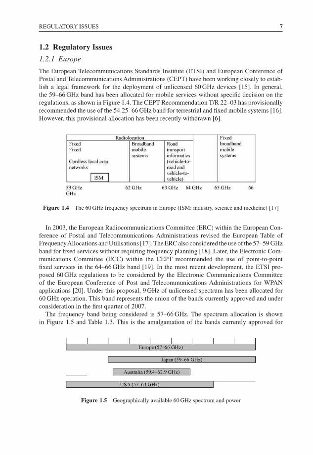
The European Telecommunications Standards Institute (ETSI) and European Conference ofPostal and Telecommunications Administrations (CEPT) have been working closely to estab-lish a legal framework for the deployment of unlicensed 60 GHz devices [15]. In general,the 59–66 GHz band has been allocated for mobile services without specific decision on theregulations, as shown in Figure 1.4. The CEPT Recommendation T/R 22–03 has provisionallyrecommended the use of the 54.25–66 GHz band for terrestrial and fixed mobile systems [16].However, this provisional allocation has been recently withdrawn [6].
Figure 1.4 The 60 GHz frequency spectrum in Europe (ISM: industry, science and medicine) [17]
In 2003, the European Radiocommunications Committee (ERC) within the European Con-ference of Postal and Telecommunications Administrations revised the European Table ofFrequencyAllocations and Utilisations [17]. The ERC also considered the use of the 57–59 GHzband for fixed services without requiring frequency planning [18]. Later, the Electronic Com-munications Committee (ECC) within the CEPT recommended the use of point-to-pointfixed services in the 64–66 GHz band [19]. In the most recent development, the ETSI pro-posed 60 GHz regulations to be considered by the Electronic Communications Committeeof the European Conference of Post and Telecommunications Administrations for WPANapplications [20]. Under this proposal, 9 GHz of unlicensed spectrum has been allocated for60 GHz operation. This band represents the union of the bands currently approved and underconsideration in the first quarter of 2007.
The frequency band being considered is 57–66 GHz. The spectrum allocation is shownin Figure 1.5 and Table 1.3. This is the amalgamation of the bands currently approved for
Figure 1.5 Geographically available 60 GHz spectrum and power
8 GIGABIT WIRELESS COMMUNICATIONS
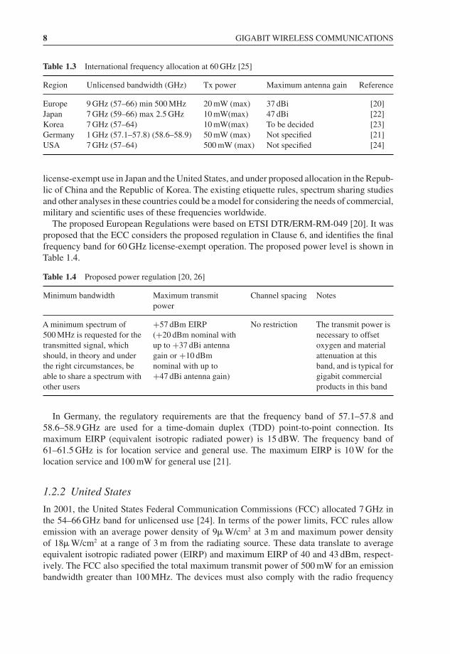
Table 1.3 International frequency allocation at 60 GHz [25]
Region Unlicensed bandwidth (GHz) Tx power Maximum antenna gain Reference
Europe 9 GHz (57–66) min 500 MHz 20 mW (max) 37 dBi [20]Japan 7 GHz (59–66) max 2.5 GHz 10 mW(max) 47 dBi [22]Korea 7 GHz (57–64) 10 mW(max) To be decided [23]Germany 1 GHz (57.1–57.8) (58.6–58.9) 50 mW (max) Not specified [21]USA 7 GHz (57–64) 500 mW (max) Not specified [24]
license-exempt use in Japan and the United States, and under proposed allocation in the Repub-lic of China and the Republic of Korea. The existing etiquette rules, spectrum sharing studiesand other analyses in these countries could be a model for considering the needs of commercial,military and scientific uses of these frequencies worldwide.
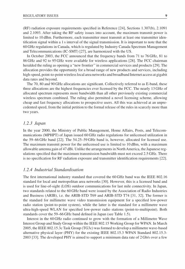
The proposed European Regulations were based on ETSI DTR/ERM-RM-049 [20]. It wasproposed that the ECC considers the proposed regulation in Clause 6, and identifies the finalfrequency band for 60 GHz license-exempt operation. The proposed power level is shown inTable 1.4.
Table 1.4 Proposed power regulation [20, 26]
Minimum bandwidth Maximum transmitpower
Channel spacing Notes
A minimum spectrum of500 MHz is requested for thetransmitted signal, whichshould, in theory and underthe right circumstances, beable to share a spectrum withother users
+57 dBm EIRP(+20 dBm nominal withup to +37 dBi antennagain or +10 dBmnominal with up to+47 dBi antenna gain)
No restriction The transmit power isnecessary to offsetoxygen and materialattenuation at thisband, and is typical forgigabit commercialproducts in this band
In Germany, the regulatory requirements are that the frequency band of 57.1–57.8 and58.6–58.9 GHz are used for a time-domain duplex (TDD) point-to-point connection. Itsmaximum EIRP (equivalent isotropic radiated power) is 15 dBW. The frequency band of61–61.5 GHz is for location service and general use. The maximum EIRP is 10 W for thelocation service and 100 mW for general use [21].
1.2.2 United States
In 2001, the United States Federal Communication Commissions (FCC) allocated 7 GHz inthe 54–66 GHz band for unlicensed use [24]. In terms of the power limits, FCC rules allowemission with an average power density of 9� W/cm2 at 3 m and maximum power densityof 18� W/cm2 at a range of 3 m from the radiating source. These data translate to averageequivalent isotropic radiated power (EIRP) and maximum EIRP of 40 and 43 dBm, respect-ively. The FCC also specified the total maximum transmit power of 500 mW for an emissionbandwidth greater than 100 MHz. The devices must also comply with the radio frequency
REGULATORY ISSUES 9
(RF) radiation exposure requirements specified in Reference [24], Sections 1.307(b), 2.1091and 2.1093. After taking the RF safety issues into account, the maximum transmit power islimited to 10 dBm. Furthermore, each transmitter must transmit at least one transmitter iden-tification signal within a 1 s interval of the signal transmission. It is important to note that the60 GHz regulations in Canada, which is regulated by Industry Canada Spectrum Managementand Telecommunications (IC-SMT) [27], are harmonized with the US.
In October 2003, the FCC announced that the frequency bands from 71 to 76 GHz, 81 to86 GHz and 92 to 95 GHz were available for wireless applications [28]. The FCC chairmanheralded the ruling as opening a “new frontier’’ in commercial services and products [29]. Theallocation provides the opportunity for a broad range of new products and services, includinghigh-speed, point-to-point wireless local area networks and broadband Internet access at gigabitdata rates and beyond.
The 70, 80 and 90 GHz allocations are significant. Collectively referred to as E-band, thesethree allocations are the highest frequencies ever licensed by the FCC. The nearly 13 GHz ofallocated spectrum represents more bandwidth than all other previously existing commercialwireless spectrum combined. The ruling also permitted a novel licensing scheme, allowingcheap and fast frequency allocations to prospective users. All this was achieved at an unpre-cedented speed, from the initial petition to the formal release of the rules in scarcely more thantwo years.
1.2.3 Japan
In the year 2000, the Ministry of Public Management, Home Affairs, Posts, and Telecom-munications (MPHPT) of Japan issued 60 GHz radio regulations for unlicensed utilization inthe 59–66 GHz band [22]. The 54.25–59 GHz band is, however, allocated for licensed use.The maximum transmit power for the unlicensed use is limited to 10 dBm, with a maximumallowable antenna gain of 47 dBi. Unlike the arrangements in NorthAmerica, the Japanese reg-ulations specified that the maximum transmission bandwidth must not exceed 2.5 GHz. Thereis no specification for RF radiation exposure and transmitter identification requirements [22].
1.2.4 Industrial Standardisation
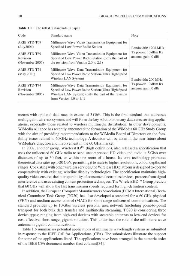
The first international industry standard that covered the 60 GHz band was the IEEE 802.16standard for local and metropolitan area networks [30]. However, this is a licensed band andis used for line-of-sight (LOS) outdoor communications for last mile connectivity. In Japan,two standards related to the 60 GHz band were issued by the Association of Radio Industriesand Business (ARIB), i.e. the ARIB-STD T69 and ARIB-STD T74 [31, 32]. The former isthe standard for millimetre wave video transmission equipment for a specified low-powerradio station (point-to-point system), while the latter is the standard for a millimetre waveultra-high-speed WLAN for specified low-power radio stations (point-to-multipoint). Bothstandards cover the 59–66 GHz band defined in Japan (see Table 1.5).
Interest in the 60 GHz radio continued to grow with the formation of a Millimetre WaveInterest Group and Study Group within the IEEE 802.15 Working Group for WPAN. In March2005, the IEEE 802.15.3c Task Group (TG3c) was formed to develop a millimetre wave-basedalternative physical layer (PHY) for the existing IEEE 802.15.3 WPAN Standard 802.15.3-2003 [33]. The developed PHY is aimed to support a minimum data rate of 2 Gb/s over a few
10 GIGABIT WIRELESS COMMUNICATIONS
Table 1.5 The 60 GHz standards in Japan
Code Standard name Note
ARIB STD-T69(July2004)
Millimetre-Wave Video Transmission Equipment forSpecified Low Power Radio Station Bandwidth: 1208 MHz
Tx power: 10 dBm Rxantenna gain: 0 dBi
ARIB STD-T69Revision(November 2005)
Millimetre-Wave Video Transmission Equipment forSpecified Low Power Radio Station (only the part ofthe revision from Version 2.0 to 2.1)
ARIB STD-T74(May 2001)
Millimetre-Wave Data Transmission Equipment forSpecified Low Power Radio Station (Ultra High SpeedWireless LAN System) Bandwidth: 200 MHz
Tx power: 10 dBm Rxantenna gain: 0 dBi
ARIB STD-T74Revision(November 2005)
Millimetre-Wave Data Transmission Equipment forSpecified Low Power Radio Station (Ultra High SpeedWireless LAN System) (only the part of the revisionfrom Version 1.0 to 1.1)
metres with optional data rates in excess of 3 Gb/s. This is the first standard that addressesmultigigabit wireless systems and will form the key solution to many data rates serving applic-ations, especially those related to wireless multimedia distribution. In other developments,WiMedia Alliance has recently announced the formation of the WiMedia 60 GHz Study Groupwith the aim of providing recommendations to the WiMedia Board of Directors on the feas-ibility issues related to 60 GHz technology. A decision will be taken in the near future aboutWiMedia’s direction and involvement in the 60 GHz market.
In 2007, another group, WirelessHDTM (high definition), also released a specification thatuses the unlicensed 60 GHz radio to send uncompressed HD video and audio at 5 Gb/s overdistances of up to 30 feet, or within one room of a house. Its core technology promotestheoretical data rates up to 20 Gb/s, permitting it to scale to higher resolutions, colour depths andranges. Coexisting with other wireless services, the Wireless HD platform is designed to operatecooperatively with existing, wireline display technologies. The specification maintains high-quality video, ensures the interoperability of consumer electronics devices, protects from signalinterference and uses existing content protection techniques. The WirelessHDTM Group predictsthat 60 GHz will allow the fast transmission speeds required for high-definition content.
In addition, the European Computer ManufacturersAssociation (ECMAInternational) Tech-nical Committee Task Group (TG20) has also developed a standard for a 60 GHz physical(PHY) and medium access control (MAC) for short-range unlicensed communications. Thestandard provides up to 10 Gb/s wireless personal area network (including point-to-point)transport for both bulk data transfer and multimedia streaming. TG20 is considering threedevice types; ranging from high-end devices with steerable antennas to low-end devices forcost effective, short range, gigabit solutions. This underlines the role of the millimetre waveantenna in gigabit communications.
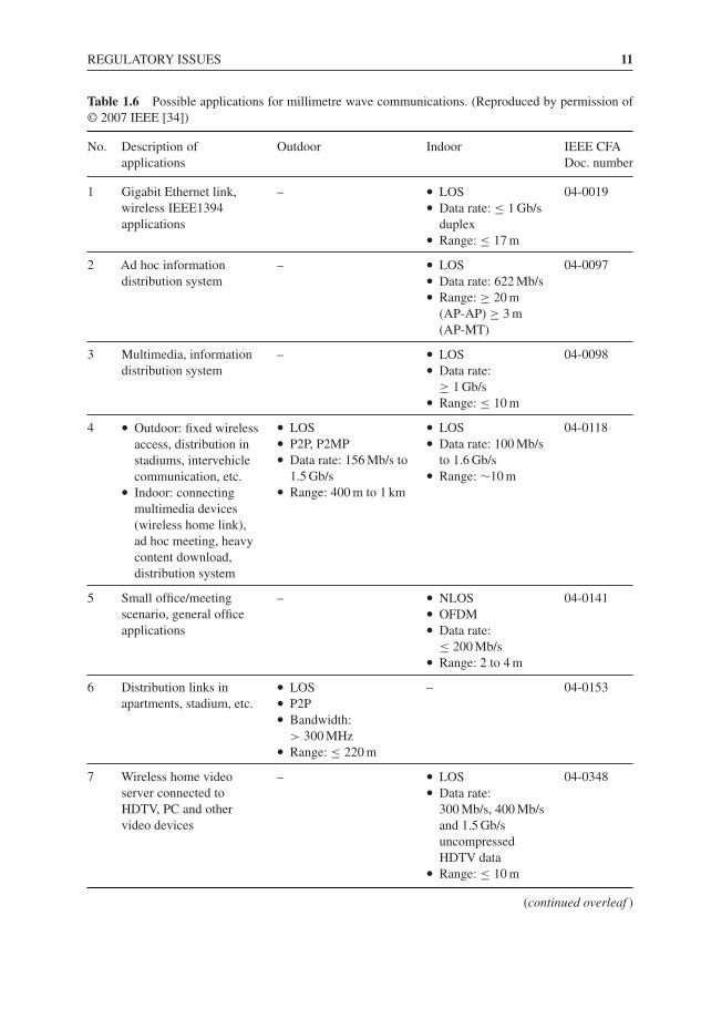
Table 1.6 summarises potential applications of millimetre wavelength systems as submittedin response to the IEEE Call for Applications (CFA). The submissions illustrate the supportfor some of the applications listed. The applications have been arranged in the numeric orderof the IEEE CFA document number (last column)[34].
REGULATORY ISSUES 11
Table 1.6 Possible applications for millimetre wave communications. (Reproduced by permission of© 2007 IEEE [34])
No. Description ofapplications
Outdoor Indoor IEEE CFADoc. number
1 Gigabit Ethernet link,wireless IEEE1394applications
– • LOS• Data rate: ≤ 1 Gb/s
duplex• Range: ≤ 17 m
04-0019
2 Ad hoc informationdistribution system
– • LOS• Data rate: 622 Mb/s• Range: ≥ 20 m
(AP-AP) ≥ 3 m(AP-MT)
04-0097
3 Multimedia, informationdistribution system
– • LOS• Data rate:
≥ 1 Gb/s• Range: ≤ 10 m
04-0098
4 • Outdoor: fixed wirelessaccess, distribution instadiums, intervehiclecommunication, etc.
• Indoor: connectingmultimedia devices(wireless home link),ad hoc meeting, heavycontent download,distribution system
• LOS• P2P, P2MP• Data rate: 156 Mb/s to
1.5 Gb/s• Range: 400 m to 1 km
• LOS• Data rate: 100 Mb/s
to 1.6 Gb/s• Range: ∼10 m
04-0118
5 Small office/meetingscenario, general officeapplications
– • NLOS• OFDM• Data rate:
≤ 200 Mb/s• Range: 2 to 4 m
04-0141
6 Distribution links inapartments, stadium, etc.
• LOS• P2P• Bandwidth:
> 300 MHz• Range: ≤ 220 m
– 04-0153
7 Wireless home videoserver connected toHDTV, PC and othervideo devices
– • LOS• Data rate:
300 Mb/s, 400 Mb/sand 1.5 Gb/suncompressedHDTV data
• Range: ≤ 10 m
04-0348
(continued overleaf )
12 GIGABIT WIRELESS COMMUNICATIONS
Table 1.6 (continued)
No. Description of applications Outdoor Indoor IEEE CFADoc. number
8 • Outdoor: distribution linksin apartments, stadium,etc.
• Indoor: ad hoc network
• LOS• P2P and P2MP• Bandwidth:
> 300 MHz• Range: ≤ 220 m
• LOS• Data rate: ≥ 1 Gb/s
and ≥ 622 Mb/s• Range: ≥ 20 m and
≥ 3 m
04-0352
9 PowerPoint and suchapplications
– • LOS and NLOS• Data rate: ≥ 1 Gb/s• Range: ≤ 3 m• Space diversity
04-0514
10 • Replacement for 1394FireWire
• Replacement for USB• Military – future combat
systems, securecommunication
– • LOS and NLOS(people)
• 100 to 500 Mb/slink, 1 Gb/s in 2007
• Short range
04-0665
1.3 Millimetre Wave Characterisations
This section presents benefits of 60 GHz technology and its major characteristics. It can beused for high-speed Internet, data and voice communications, and offers the following keybenefits:
1. Unlicensed operation2. Highly secure operation: resulting from short transmission distances due to oxygen
absorption, narrow antenna beamwidth and no wall penetration3. Virtually interference-free operation: resulting from short transmission distances due to
oxygen absorption, narrow antenna beam width and limited use of 60 GHz spectrum4. High level of frequency re-use enabled: the communication needs of multiple customers
within a small geographic region can be satisfied5. Fibre optic data transmission speeds possible: 7 GHz (in the USA) of continuous bandwidth
available compared to < 0.3 GHz at the other unlicensed bands (3.5 GHz internationallyavailable)
6. Mature technology: long history of this spectrum being used for secure communications7. Carrier-class communication links enabled: 60 GHz links can be engineered to deliver “five
nines’’ (99.999 %) availability if desired (outdoor applications such as backbone or bypassbridges)
There is a widespread belief that the characteristics of a millimetre wave present manydifficulties in terms of propagation environment for high data rate wireless communications.
MILLIMETRE WAVE CHARACTERISATIONS 13
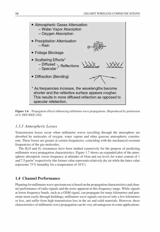
While the oxygen absorption does indeed cause a 15 dB/km loss, this translates to only a1.5 dB loss at 100 m, so for indoor applications the absorption loss from oxygen is small, ifnot negligible.
Another loss – proportional to the frequency squared – comes from the Friis path lossequation (1.2). This “loss’’, however, can be attributed to another factor. If omni-directionalantennas, such as half-wavelength dipoles, are used, then as the frequency rises, the effectivearea of the antennas decreases as frequency squared. If, on the other hand, the (physical) areaof the antennas is kept constant, then there is no increase in path loss because the electricalarea increases as the wavelength decreases (squared).
For instance, a 60 GHz antenna, which has an effective area of 1 square inch, will have again of approximately 25 dBi, but this gain comes at the expense of being highly directional.This would mean that for millimetre wave radios to be used at their full potential they wouldneed a solution for precise pointing.
1.3.1 Free Space Propagation
As with all propagating electromagnetic waves, for millimetre waves in free space the powerflux density falls off as the square of range. For a doubling of range, power flux density at areceiver antenna is reduced by a factor of four. This effect is due to the spherical spreading ofthe radio waves as they propagate. The frequency and distance dependence of the loss betweentwo isotropic antennas can be expressed in absolute numbers by (in dB):
Lfree space = 20 log10
(4π
R
λ
)(dB) (1.1)
where Lfree space is the freespace loss, R is the distance between transmit and receive antennas,and λ is the operating wavelength. This equation describes line-of-sight wave propagation infree space. This equation shows that the free space loss increases when the frequency or rangeincreases. Thus, millimetre wave free space loss can be quite high, even for short distances.This indicates that the millimetrewave spectrum is best used for short-distance communicationslinks. The Friis equation (1946) gives a more complete expression for all the factors from thetransmitter to the receiver (as a ratio, linear units) [35]:
PRx = PT xGRxGT x
λ2
(4πR)2L(1.2)
where GT X = transmitter antenna gain, GRX = receiver antenna gain, λ = wavelength (in thesame units as R), R = line-of-sight (LOS) distance separating transmit and receive antennasand L = system loss factor (≥ 1).
1.3.2 Millimetre Wave Propagation Loss Factors
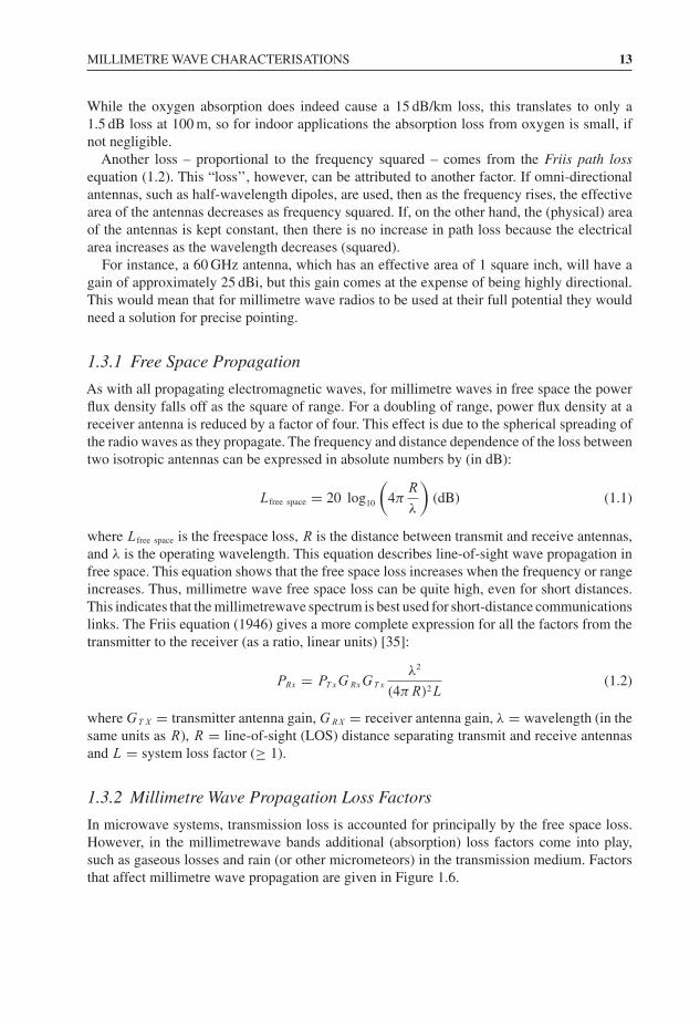
In microwave systems, transmission loss is accounted for principally by the free space loss.However, in the millimetrewave bands additional (absorption) loss factors come into play,such as gaseous losses and rain (or other micrometeors) in the transmission medium. Factorsthat affect millimetre wave propagation are given in Figure 1.6.
14 GIGABIT WIRELESS COMMUNICATIONS
Figure 1.6 Propagation effects influencing millimetre wave propagations. (Reproduced by permissionof © 2005 IEEE [36])
1.3.3 Atmospheric Losses
Transmission losses occur when millimetre waves travelling through the atmosphere areabsorbed by molecules of oxygen, water vapour and other gaseous atmospheric constitu-ents. These losses are greater at certain frequencies, coinciding with the mechanical resonantfrequencies of the gas molecules.
The H2O and O2 resonances have been studied extensively for the purpose of predictingmillimetre wave propagation characteristics. Figure 1.7 shows an expanded plot of the atmo-spheric absorption versus frequency at altitudes of 4 km and sea level, for water content of 1and 7.5 gm/m3 respectively (the former value represents relatively dry air while the latter valuerepresents 75 % humidity for a temperature of 10◦C).
1.4 Channel Performance
Planning for millimetre wave spectrum use is based on the propagation characteristics and chan-nel performance of radio signals and the noise apparent in this frequency range. While signalsat lower frequency bands, such as a GSM signal, can propagate for many kilometres and pen-etrate more easily through buildings, millimetre wave signals can travel only a few kilometresor less, and suffer from high transmission loss in the air and solid materials. However, thesecharacteristics of millimetre wave propagation can be very advantageous in some applications.
CHANNEL PERFORMANCE 15
Figure 1.7 Average atmospheric absorption of millimetre waves. (Reproduced by permission of ©2005 IEEE [36])
Millimetre waves can establish more densely packed communications links, thus providingvery efficient spectrum utilization; the high absorption enabling shorter range frequency re-use,and therefore increasing the overall capacity of communication systems. The characteristics ofmillimetre wave propagation are summarised in this section, including free space propagationand the effects of various physical factors on propagation.
The main challenges for a 60 GHz channel can be described as follows:
• High loss from the Friis equation• Doppler shift is non-negligible at pedestrian velocities• Human shadowing• Non-line-of-sight propagation, which induces random fluctuations in the signal level, known
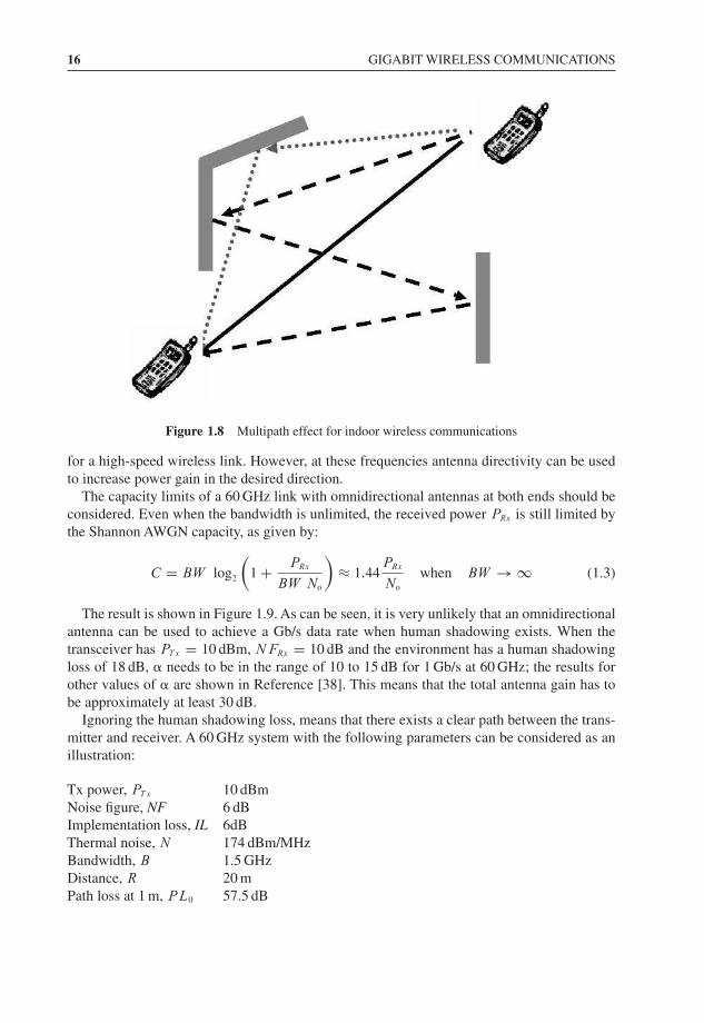
as multipath fading, as shown in Figure 1.8• Noise
The transmitting power of a 60 GHz communications link is restricted to +40 dBmEIRP limit by the FCC in the USA. Transmitter power and path loss can be limiting factors
16 GIGABIT WIRELESS COMMUNICATIONS
Figure 1.8 Multipath effect for indoor wireless communications
for a high-speed wireless link. However, at these frequencies antenna directivity can be usedto increase power gain in the desired direction.
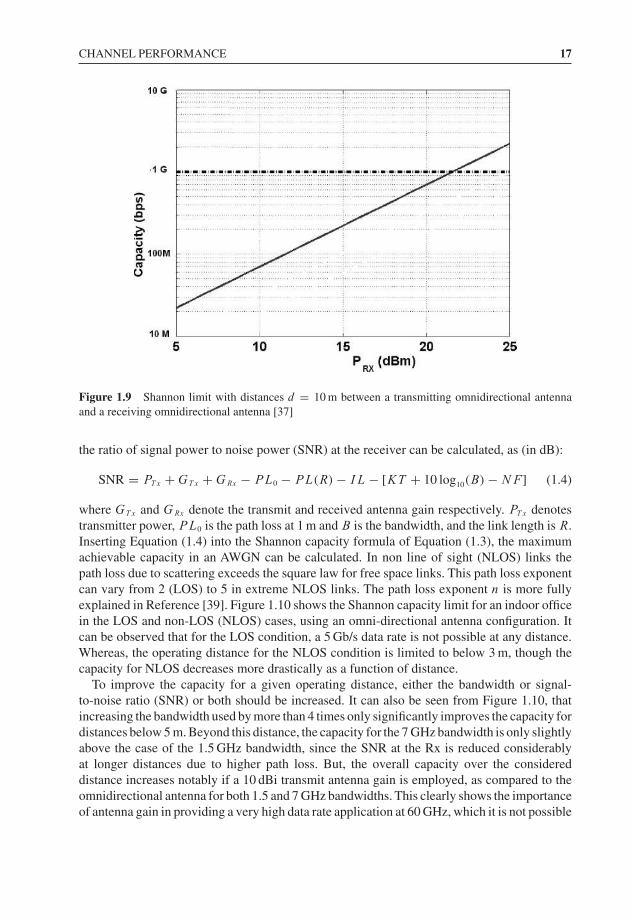
The capacity limits of a 60 GHz link with omnidirectional antennas at both ends should beconsidered. Even when the bandwidth is unlimited, the received power PRx is still limited bythe Shannon AWGN capacity, as given by:
C = BW log2
(1 + PRx
BW No
)≈ 1.44
PRx
No
when BW → ∞ (1.3)
The result is shown in Figure 1.9. As can be seen, it is very unlikely that an omnidirectionalantenna can be used to achieve a Gb/s data rate when human shadowing exists. When thetransceiver has PT x = 10 dBm, NFRx = 10 dB and the environment has a human shadowingloss of 18 dB, � needs to be in the range of 10 to 15 dB for 1 Gb/s at 60 GHz; the results forother values of � are shown in Reference [38]. This means that the total antenna gain has tobe approximately at least 30 dB.
Ignoring the human shadowing loss, means that there exists a clear path between the trans-mitter and receiver. A 60 GHz system with the following parameters can be considered as anillustration:
Tx power, PT x 10 dBmNoise figure, NF 6 dBImplementation loss, IL 6dBThermal noise, N 174 dBm/MHzBandwidth, B 1.5 GHzDistance, R 20 mPath loss at 1 m, P L0 57.5 dB
CHANNEL PERFORMANCE 17
Figure 1.9 Shannon limit with distances d = 10 m between a transmitting omnidirectional antennaand a receiving omnidirectional antenna [37]
the ratio of signal power to noise power (SNR) at the receiver can be calculated, as (in dB):
SNR = PT x + GT x + GRx − P L0 − P L(R) − IL − [KT + 10 log10(B) − NF ] (1.4)
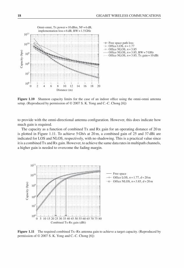
where GT x and GRx denote the transmit and received antenna gain respectively. PT x denotestransmitter power, P L0 is the path loss at 1 m and B is the bandwidth, and the link length is R.Inserting Equation (1.4) into the Shannon capacity formula of Equation (1.3), the maximumachievable capacity in an AWGN can be calculated. In non line of sight (NLOS) links thepath loss due to scattering exceeds the square law for free space links. This path loss exponentcan vary from 2 (LOS) to 5 in extreme NLOS links. The path loss exponent n is more fullyexplained in Reference [39]. Figure 1.10 shows the Shannon capacity limit for an indoor officein the LOS and non-LOS (NLOS) cases, using an omni-directional antenna configuration. Itcan be observed that for the LOS condition, a 5 Gb/s data rate is not possible at any distance.Whereas, the operating distance for the NLOS condition is limited to below 3 m, though thecapacity for NLOS decreases more drastically as a function of distance.
To improve the capacity for a given operating distance, either the bandwidth or signal-to-noise ratio (SNR) or both should be increased. It can also be seen from Figure 1.10, thatincreasing the bandwidth used by more than 4 times only significantly improves the capacity fordistances below 5 m. Beyond this distance, the capacity for the 7 GHz bandwidth is only slightlyabove the case of the 1.5 GHz bandwidth, since the SNR at the Rx is reduced considerablyat longer distances due to higher path loss. But, the overall capacity over the considereddistance increases notably if a 10 dBi transmit antenna gain is employed, as compared to theomnidirectional antenna for both 1.5 and 7 GHz bandwidths. This clearly shows the importanceof antenna gain in providing a very high data rate application at 60 GHz, which it is not possible
18 GIGABIT WIRELESS COMMUNICATIONS
0106
107
108
109
1010
1011
2 4 6 8 10 12 14 16 18 20Distance (m)
Cap
acity
(bp
s)
Omni-omni, Tx power = 10 dBm, NF = 6 dB,implementation loss = 6 dB, BW = 1.5 GHz
Free space path lossOffice LOS, n = 1.77Office NLOS, n = 3.85Office NLOS, n = 3.85, BW = 7 GHzOffice NLOS, n = 3.85, Tx gain = 10 dBi
Figure 1.10 Shannon capacity limits for the case of an indoor office using the omni-omni antennasetup. (Reproduced by permission of © 2007 S. K. Yong and C.-C. Chong [6])
to provide with the omni-directional antenna configuration. However, this does indicate howmuch gain is required.
The capacity as a function of combined Tx and Rx gain for an operating distance of 20 mis plotted in Figure 1.11. To achieve 5 Gb/s at 20 m, a combined gain of 25 and 37 dBi areindicated for LOS and NLOS, respectively, with no shadowing. This is a practical value sinceit is a combined Tx and Rx gain. However, to achieve the same data rates in multipath channels,a higher gain is needed to overcome the fading margin.
0106
107
108
109
1010
1011
5 10 15 20 25 30 35 40 45 50 55 60 65 70 75 80Combined Tx-Rx gain (dBi)
Cap
acity
(bp
s)
Free spaceOffice LOS, n = 1.77, d = 20 mOffice NLOS, n = 3.85, d = 20 m
Figure 1.11 The required combined Tx–Rx antenna gain to achieve a target capacity. (Reproduced bypermission of © 2007 S. K. Yong and C.-C. Chong [6])
CHANNEL PERFORMANCE 19
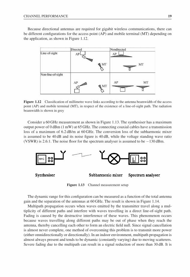
Because directional antennas are required for gigabit wireless communications, there canbe different configurations for the access point (AP) and mobile terminal (MT) depending onthe application, as shown in Figure 1.12.
Figure 1.12 Classification of millimetre wave links according to the antenna beamwidth of the accesspoint (AP) and mobile terminal (MT), in respect of the existence of a line-of-sight path. The radiationbeamwidth is shown in grey
Consider a 60 GHz measurement as shown in Figure 1.13. The synthesiser has a maximumoutput power of 0 dBm (1 mW) at 65 GHz. The connecting coaxial cables have a transmissionloss of a maximum of 6.2 dB/m at 60 GHz. The conversion loss of the subharmonic mixeris assumed to be 40 dB and its noise figure is 40 dB, while the voltage standing wave ratio(VSWR) is 2.6:1. The noise floor for the spectrum analyser is assumed to be −130 dBm.
Figure 1.13 Channel measurement setup
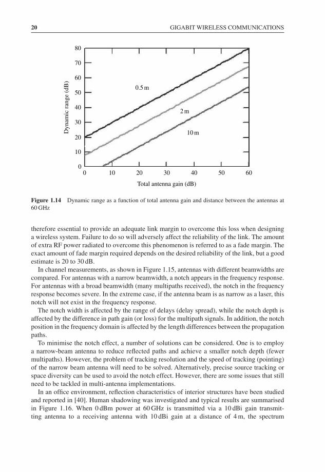
The dynamic range for this configuration can be measured as a function of the total antennagain and the separation of the antennas at 60 GHz. The result is shown in Figure 1.14.
Multipath propagation occurs when waves emitted by the transmitter travel along a mul-tiplicity of different paths and interfere with waves travelling in a direct line-of-sight path.Fading is caused by the destructive interference of these waves. This phenomenon occursbecause waves travelling along different paths may be out of phase when they reach theantenna, thereby cancelling each other to form an electric field null. Since signal cancellationis almost never complete, one method of overcoming this problem is to transmit more power(either omnidirectionally or directionally). In an indoor environment, multipath propagation isalmost always present and tends to be dynamic (constantly varying) due to moving scatterers.Severe fading due to the multipath can result in a signal reduction of more than 30 dB. It is
20 GIGABIT WIRELESS COMMUNICATIONS
00
10
20
30
40
50
60
70
80
Dyn
amic
ran
ge (
dB)
10 20
0.5 m
2 m
10 m
30 40 50 60
Total antenna gain (dB)
Figure 1.14 Dynamic range as a function of total antenna gain and distance between the antennas at60 GHz
therefore essential to provide an adequate link margin to overcome this loss when designinga wireless system. Failure to do so will adversely affect the reliability of the link. The amountof extra RF power radiated to overcome this phenomenon is referred to as a fade margin. Theexact amount of fade margin required depends on the desired reliability of the link, but a goodestimate is 20 to 30 dB.
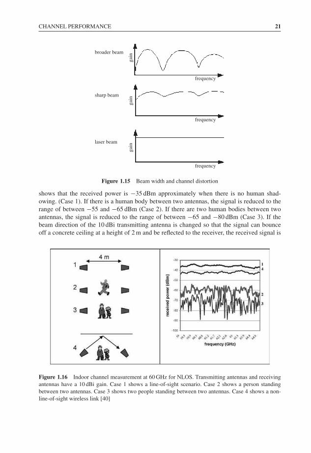
In channel measurements, as shown in Figure 1.15, antennas with different beamwidths arecompared. For antennas with a narrow beamwidth, a notch appears in the frequency response.For antennas with a broad beamwidth (many multipaths received), the notch in the frequencyresponse becomes severe. In the extreme case, if the antenna beam is as narrow as a laser, thisnotch will not exist in the frequency response.
The notch width is affected by the range of delays (delay spread), while the notch depth isaffected by the difference in path gain (or loss) for the multipath signals. In addition, the notchposition in the frequency domain is affected by the length differences between the propagationpaths.
To minimise the notch effect, a number of solutions can be considered. One is to employa narrow-beam antenna to reduce reflected paths and achieve a smaller notch depth (fewermultipaths). However, the problem of tracking resolution and the speed of tracking (pointing)of the narrow beam antenna will need to be solved. Alternatively, precise source tracking orspace diversity can be used to avoid the notch effect. However, there are some issues that stillneed to be tackled in multi-antenna implementations.
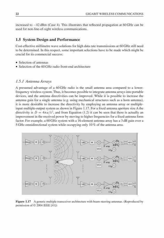
In an office environment, reflection characteristics of interior structures have been studiedand reported in [40]. Human shadowing was investigated and typical results are summarisedin Figure 1.16. When 0 dBm power at 60 GHz is transmitted via a 10 dBi gain transmit-ting antenna to a receiving antenna with 10 dBi gain at a distance of 4 m, the spectrum
CHANNEL PERFORMANCE 21
frequency
frequency
frequency
gain
gain
gain
broader beam
sharp beam
laser beam
Figure 1.15 Beam width and channel distortion
shows that the received power is −35 dBm approximately when there is no human shad-owing. (Case 1). If there is a human body between two antennas, the signal is reduced to therange of between −55 and −65 dBm (Case 2). If there are two human bodies between twoantennas, the signal is reduced to the range of between −65 and −80 dBm (Case 3). If thebeam direction of the 10 dBi transmitting antenna is changed so that the signal can bounceoff a concrete ceiling at a height of 2 m and be reflected to the receiver, the received signal is
Figure 1.16 Indoor channel measurement at 60 GHz for NLOS. Transmitting antennas and receivingantennas have a 10 dBi gain. Case 1 shows a line-of-sight scenario. Case 2 shows a person standingbetween two antennas. Case 3 shows two people standing between two antennas. Case 4 shows a non-line-of-sight wireless link [40]
22 GIGABIT WIRELESS COMMUNICATIONS
increased to −42 dBm (Case 4). This illustrates that reflected propagation at 60 GHz can beused for non-line-of-sight wireless communications.
1.5 System Design and Performance
Cost-effective millimetre wave solutions for high data rate transmissions at 60 GHz still needto be determined. In this respect, some important selections have to be made which might becrucial for its commercial success:
• Selection of antennas• Selection of the 60 GHz radio front-end architecture
1.5.1 Antenna Arrays
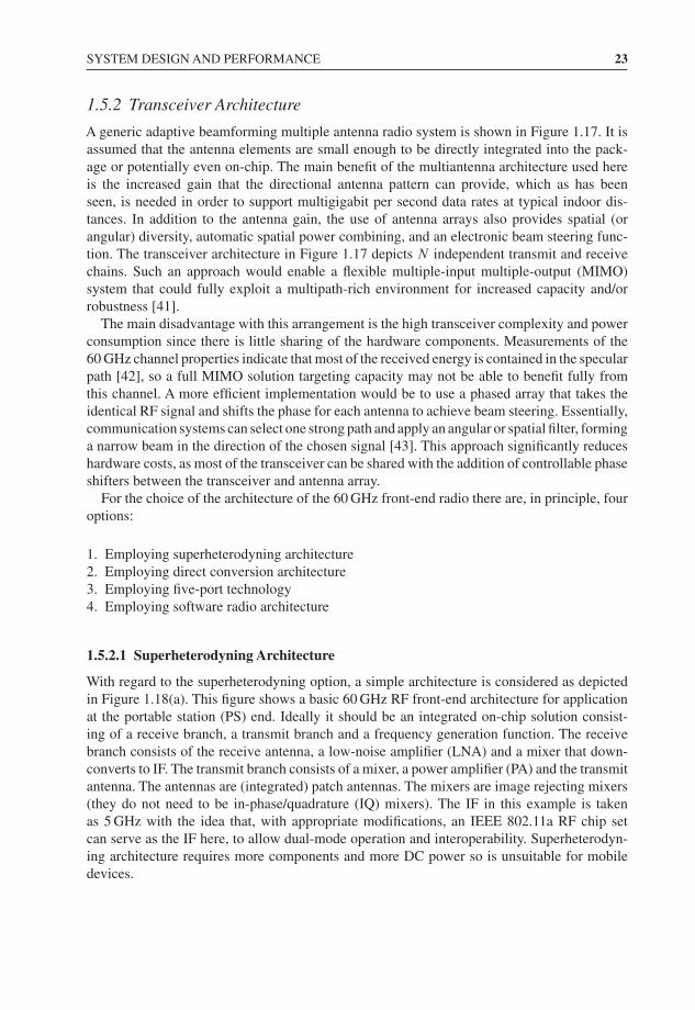
A presumed advantage of a 60 GHz radio is the small antenna area compared to a lower-frequency wireless system. Thus, it becomes possible to integrate antenna arrays into portabledevices, and the antenna directivities can be improved. While it is possible to increase theantenna gain for a single antenna (e.g. using mechanical structures such as a horn antenna),it is more desirable to increase the directivity by employing an antenna array or multiple-input multiple-output system as shown in Figure 1.17. For a fixed antenna aperture size A thedirectivity is D = 4πa/λ2, and from Equation (1.2) it can be seen that there is actually animprovement in the received power by moving to higher frequencies for a fixed antenna formfactor. For example, a 60 GHz system with a 16-element antenna array has a 3 dB gain over a5 GHz omnidirectional system while occupying only 10 % of the antenna area.
Figure 1.17 A generic multiple transceiver architecture with beam-steering antennas. (Reproduced bypermission of © 2004 IEEE [41])
SYSTEM DESIGN AND PERFORMANCE 23
1.5.2 Transceiver Architecture
A generic adaptive beamforming multiple antenna radio system is shown in Figure 1.17. It isassumed that the antenna elements are small enough to be directly integrated into the pack-age or potentially even on-chip. The main benefit of the multiantenna architecture used hereis the increased gain that the directional antenna pattern can provide, which as has beenseen, is needed in order to support multigigabit per second data rates at typical indoor dis-tances. In addition to the antenna gain, the use of antenna arrays also provides spatial (orangular) diversity, automatic spatial power combining, and an electronic beam steering func-tion. The transceiver architecture in Figure 1.17 depicts N independent transmit and receivechains. Such an approach would enable a flexible multiple-input multiple-output (MIMO)system that could fully exploit a multipath-rich environment for increased capacity and/orrobustness [41].
The main disadvantage with this arrangement is the high transceiver complexity and powerconsumption since there is little sharing of the hardware components. Measurements of the60 GHz channel properties indicate that most of the received energy is contained in the specularpath [42], so a full MIMO solution targeting capacity may not be able to benefit fully fromthis channel. A more efficient implementation would be to use a phased array that takes theidentical RF signal and shifts the phase for each antenna to achieve beam steering. Essentially,communication systems can select one strong path and apply an angular or spatial filter, forminga narrow beam in the direction of the chosen signal [43]. This approach significantly reduceshardware costs, as most of the transceiver can be shared with the addition of controllable phaseshifters between the transceiver and antenna array.
For the choice of the architecture of the 60 GHz front-end radio there are, in principle, fouroptions:
1. Employing superheterodyning architecture2. Employing direct conversion architecture3. Employing five-port technology4. Employing software radio architecture
1.5.2.1 Superheterodyning Architecture
With regard to the superheterodyning option, a simple architecture is considered as depictedin Figure 1.18(a). This figure shows a basic 60 GHz RF front-end architecture for applicationat the portable station (PS) end. Ideally it should be an integrated on-chip solution consist-ing of a receive branch, a transmit branch and a frequency generation function. The receivebranch consists of the receive antenna, a low-noise amplifier (LNA) and a mixer that down-converts to IF. The transmit branch consists of a mixer, a power amplifier (PA) and the transmitantenna. The antennas are (integrated) patch antennas. The mixers are image rejecting mixers(they do not need to be in-phase/quadrature (IQ) mixers). The IF in this example is takenas 5 GHz with the idea that, with appropriate modifications, an IEEE 802.11a RF chip setcan serve as the IF here, to allow dual-mode operation and interoperability. Superheterodyn-ing architecture requires more components and more DC power so is unsuitable for mobiledevices.
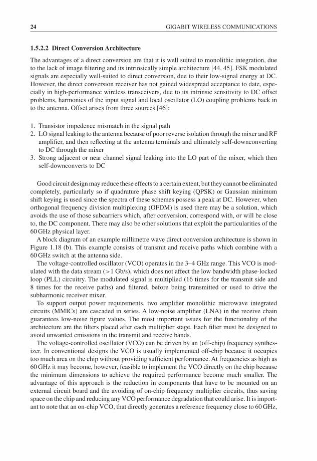
24 GIGABIT WIRELESS COMMUNICATIONS
1.5.2.2 Direct Conversion Architecture
The advantages of a direct conversion are that it is well suited to monolithic integration, dueto the lack of image filtering and its intrinsically simple architecture [44, 45]. FSK modulatedsignals are especially well-suited to direct conversion, due to their low-signal energy at DC.However, the direct conversion receiver has not gained widespread acceptance to date, espe-cially in high-performance wireless transceivers, due to its intrinsic sensitivity to DC offsetproblems, harmonics of the input signal and local oscillator (LO) coupling problems back into the antenna. Offset arises from three sources [46]:
1. Transistor impedence mismatch in the signal path2. LO signal leaking to the antenna because of poor reverse isolation through the mixer and RF
amplifier, and then reflecting at the antenna terminals and ultimately self-downconvertingto DC through the mixer
3. Strong adjacent or near channel signal leaking into the LO part of the mixer, which thenself-downconverts to DC
Good circuit design may reduce these effects to a certain extent, but they cannot be eliminatedcompletely, particularly so if quadrature phase shift keying (QPSK) or Gaussian minimumshift keying is used since the spectra of these schemes possess a peak at DC. However, whenorthogonal frequency division multiplexing (OFDM) is used there may be a solution, whichavoids the use of those subcarriers which, after conversion, correspond with, or will be closeto, the DC component. There may also be other solutions that exploit the particularities of the60 GHz physical layer.
A block diagram of an example millimetre wave direct conversion architecture is shown inFigure 1.18 (b). This example consists of transmit and receive paths which combine with a60 GHz switch at the antenna side.
The voltage-controlled oscillator (VCO) operates in the 3–4 GHz range. This VCO is mod-ulated with the data stream (>1 Gb/s), which does not affect the low bandwidth phase-lockedloop (PLL) circuitry. The modulated signal is multiplied (16 times for the transmit side and8 times for the receive paths) and filtered, before being transmitted or used to drive thesubharmonic receiver mixer.
To support output power requirements, two amplifier monolithic microwave integratedcircuits (MMICs) are cascaded in series. A low-noise amplifier (LNA) in the receive chainguarantees low-noise figure values. The most important issues for the functionality of thearchitecture are the filters placed after each multiplier stage. Each filter must be designed toavoid unwanted emissions in the transmit and receive bands.
The voltage-controlled oscillator (VCO) can be driven by an (off-chip) frequency synthes-izer. In conventional designs the VCO is usually implemented off-chip because it occupiestoo much area on the chip without providing sufficient performance. At frequencies as high as60 GHz it may become, however, feasible to implement the VCO directly on the chip becausethe minimum dimensions to achieve the required performance become much smaller. Theadvantage of this approach is the reduction in components that have to be mounted on anexternal circuit board and the avoiding of on-chip frequency multiplier circuits, thus savingspace on the chip and reducing any VCO performance degradation that could arise. It is import-ant to note that an on-chip VCO, that directly generates a reference frequency close to 60 GHz,
SYSTEM DESIGN AND PERFORMANCE 25
Figure 1.18 (a) Block diagram for millimetre wave/microwave circuits. (b) Block diagram for a 60 GHzdirect conversion architecture
may have a relatively lower performance when compared with the requirements of a VCO thatoperates on a much lower frequency in combination with a couple of frequency multipliers.
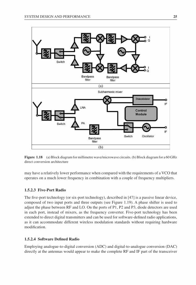
1.5.2.3 Five-Port Radio
The five-port technology (or six-port technology), described in [47] is a passive linear device,composed of two input ports and three outputs (see Figure 1.19). A phase shifter is used toadjust the phase between RF and LO. On the ports of P1, P2 and P3, diode detectors are usedin each port, instead of mixers, as the frequency converter. Five-port technology has beenextended to direct digital transmitters and can be used for software-defined radio applications,as it can accommodate different wireless modulation standards without requiring hardwaremodification.
1.5.2.4 Software Defined Radio
Employing analogue-to-digital conversion (ADC) and digital-to-analogue conversion (DAC)directly at the antennas would appear to make the complete RF and IF part of the transceiver
26 GIGABIT WIRELESS COMMUNICATIONS
Figure 1.19 Block diagram for the five-port technology
chain obsolete. However, this option for the current purpose can be ruled out immediatelybecause this would require ADC and DAC devices operating at a 60 GHz or more. A low-costimplementation of this in the medium term is not considered feasible. An alternative approach,the subsampling receiver, is claimed to represent the “ultimate’’ solution for simple low-powerdownconversion. This essentially consists of a sampling switch, clocked at a much lowerfrequency, and an analogue-to-digital (A/D) converter. The limitations of the subsamplingapproach, however, illustrate the inherent problems in low-power receiver implementations.In a subsampling receiver, image frequencies exist at integral multiples of the sampling rateand can alias (map) onto the band of interest. As a result, careful filtering prior to the down-conversion is required. For example, downconversion of an RF signal having a bandwidth of500 MHz would require a sampling rate of at least 1 GHz, assuming a “brick wall filter’’(a filterwith infinite cut off outside the working band). In practice, the sampling rate would have to bemuch higher – at least 2 GHz – in order to minimise the effects of the filter. It is questionablewhether a 2 GHz ADC with a 10 bit quantisation, will become available in the medium term. Inaddition, the signal-to-noise ratio (SNR) of the downsampled signal will inevitably be poorerthan that of an equivalent system employing a mixer for downconversion. This is due to thenoise aliased from the bands between DC and the passband [48].
1.6 Antenna Requirements
In this book, an overview is presented, of an approach within the application area that utilisesmillimetre wave antenna technology and offers significant promise in making these Gb/swireless links a reality. Throughout the book, topics will be revisited and approached fromdifferent angles in order to present alternative ways of analysing the various components andparameters that make up millimetre wave systems.
For a single antenna element with an antenna gain of more than 30 dBi with a half-powerbeamwidth (HPBW) of approximately 6.5◦, a reliable communication link is difficult to estab-lish even in a LOS condition at 60 GHz. This, as has been seen, can be due to human movementwhich can easily block and attenuate such a narrow beam signal. To overcome this problem,a switched beam antenna array or adaptive antenna array can be implemented to search and
ANTENNA REQUIREMENTS 27
beamform, in order to capture the available signal. The array is required to track the signalpath either continuously or periodically, depending on the stability of the link. One major para-meter of the performance of the link is how many antenna elements are required to achievethe intended antenna gain. This is a separate consideration from the array gain, which refersto the performance improvement in terms of the SNR over a single antenna element. Also ofinterest is the angular resolution or beamwidth of such antennas, since this defines the numberof multipaths that the antenna sees in a scattering environment. The directivity of the lineararray is given by [49]:
D = 4π∫∫ |Fn(φ, θ)|2 sin θ dθ dφ(1.5)
where Fn(ϕ, θ) is the normalized field pattern, which can be expressed as a product of thenormalized element pattern and the normalized array factor. The variables ϕ and θ representthe azimuth and elevation angle, respectively. For a uniform linear array, the normalized arrayfactor can be expressed as:
fn(ϕ, θ) = sin[(N/2)(kd cos θ + β)]N sin[(1/2)(kd cos θ + β)] (1.6)
where N , d and β are the number of antenna elements, the antenna spacing between adjacentelements and the phase shift between elements, respectively. For an omnidirectional antenna,it can be shown that up to 100 omni-element arrays are required to achieve a gain of only23 dBi, which is far from the requirement discussed previously. Hence a more directive/highergain element is required to improve the overall gain of the array.
Many types of antenna structures are considered not suitable for 60 GHz WPAN/WLANapplications due to the requirements for low cost, small size, light weight and high gain.In addition, 60 GHz antennas are also required to be operated with approximately constantgain and high efficiency over the broad frequency range (57–66 GHz). The importance ofbeamforming at 60 GHz has been introduced in Section 1.4, and can be achieved by eitherswitched beam arrays or phased arrays. Switched beam arrays have multiple fixed beams thatcan be selected to cover a given service area. They can be implemented more easily comparedto phased arrays, which require the capability of continuously varying a progressive phaseshift between the elements.
The complexity of phase arrays at 60 GHz typically limits the number of elements. In Refer-ence [50], a 2 × 2 beam-steering antenna with circular polarization at 61 GHz was developed.The gain is approximately 14 dBi with 20◦ half power beamwidth (HPBW). Similarly, inReference [51], another 60 GHz integrated four-element planar array was developed. Eachantenna is integrated with a subharmonic I/Q mixer for the convenience of high-speed signalprocessing, such as adaptive beamforming. The implementation of a larger phased array, how-ever, presents technical challenges, such as the requirement for a higher feed network loss, amore complex phase control network, stronger coupling between antennas as well as feedlines,etc. These challenges make the design and fabrication of larger phase arrays more complexand expensive. Hence, research is required to develop a low-cost, small-size, light-weight andhigh-gain steerable antenna array that can be integrated into the RF front-end electronics.
28 GIGABIT WIRELESS COMMUNICATIONS
To achieve this, the design approach can be focused on either:
(a) accepting the presence of multipath (with delays corresponding to the room size) andmitigating it with equalisation techniques or
(b) using line-of-sight links with narrow-beam antennas to eliminate virtually all multipaths,and thus use simple unequalised modulation schemes, such as FSK and PSK.
In the first case, the design effort would concentrate on narrow beam antenna design techniques,whereas in the second approach, the work would concentrate on antenna/beam-steering tech-niques. These must be used because multipath delay in the typical indoor environment is onthe order of the target bit period (tens of nanoseconds) and causes intersymbol interference.The multipath delays for indoor systems depend on the size of a room and the density andplacing of scatterers within the illuminated space.
It is assumed for the moment that for high speed data transmission a simple two- or four-level FSK or PSK system is used, because complex modulation schemes such as equalisation,diversity or multicarrier techniques are deemed to be impractical or too expensive for 60 GHz.For such a simple system to work reliably the channel impulse response should not containsignificant multipath components, so that the data rate is not limited by multipath effects.Also an initial assumption is made, that high-speed and high-capacity WLANs can use afemtocellular architecture, with a single cell for each room and multiple cells for a large openarea office.
For the “LOS with narrow beam antennas’’ approach, the amount of multipath power willdepend on the number of paths between the transmitter and receiver, which in turn will dependon the directivity of the antennas at the transmitter and receiver, as well as specific envir-onmental factors. It will also depend on the ability of the antenna to resolve the multipaths’angular space. If omnidirectional antennas are used at both the transmitter and receiver, thenthere will be many possible paths, whereas if highly directional antennas are used, there maybe only a single LOS path. Once the beamwidth is sufficiently narrow, there is no signific-ant multipath in most practical circumstances. (Of course, if the transmit and receive LOS isperpendicular to a pair of parallel reflectors an infinite number of multipaths will occur.)
To explore the consequences of this approach, three different antenna designs are nowconsidered.
1. Phased ArrayConsidering an 8 × 8 phased array antenna with beam steering, this arrangement requirescomplex phase shifters (or hybrid Tees and attenuators applied to the I and Q channels), andtherefore is subject to high loss at 60 GHz. These losses reduce the effective gain of the antennaarray. In addition, currently there is no phase shifter MMIC available at 60 GHz on the market soa hybrid Tee and real weights (attenuators) would be needed to build phase- shifting functions.In addition, the beam shape becomes asymmetric when the beam direction moves away fromthe z axis (this is generally called aberration). This means that the sidelobes of the radiationpattern will grow when the beam is away from broadside. Also, circular polarisation at wideangles with a phase-shifted array is almost impossible to achieve. The performance of circularpolarisation is unlikely to be achieved as the phased array becomes increasingly complex. Themain challenge of this design is to have a complex phase shifter and to have low loss. Lastly,it is also difficult to achieve good circular polarisation in all directions.
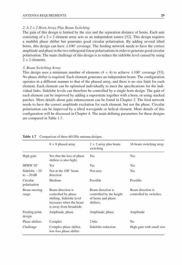
ANTENNA REQUIREMENTS 29
2. A 2 × 2 Horn Array Plus Beam SwitchingThe gain of this design is limited by the size and the separation distance of horns. Each unitconsisting of a 2 × 2 element array acts as an independent source [52]. This design requiresa multibit phase shifter but generates good circular polarisation. By adding several tiltedhorns, this design can have ±100◦ coverage. The feeding network needs to have the correctamplitude and phase in the two orthogonal linear polarisations in order to generate good circularpolarisation. The main challenge of this design is to reduce the sidelobe level caused by using2 × 2 elements.
3. Beam Switching ArrayThis design uses a minimum number of elements (4 × 4) to achieve ±100◦ coverage [53].No phase shifter is required. Each element generates an independent beam. The configurationoperates in a different manner to that of the phased array, and there is no size limit for eachelement. Each element can be optimised individually to meet the specifications for the indi-vidual links. Sidelobe levels can therefore be controlled by a single horn design. The gain ofeach element can be improved by adding a superstrate together with a horn, or using stackedpatches. More details about gain enhancement can be found in Chapter 2. The feed networkneeds to have the correct amplitude excitation for each element, but not the phase. Circularpolarisation can be improved by a tilted waveguide or helical element. More details of thisconfiguration will be discussed in Chapter 4. The main defining parameters for these designsare compared in Table 1.7.
Table 1.7 Comparison of three 60 GHz antenna designs
8 × 8 phased array 2 × 2 array plus beamswitching
16 beam switching array
High gain Yes (but the loss of phaseshifters is also high)
Yes Yes
HPBW 20◦ Yes Yes Yes
Sidelobe −10to −20 dB
Not at the 100◦ beamdirection
Not easy Yes
Circularpolarisation
Medium Possible Possible
Beam steeringrange
Beam direction iscontrolled by phaseshifting. Sidelobe levelincreases when the beamis away from broadside.
Beam direction iscontrolled by the heightof horns and phaseshifters.
Beam direction iscontrolled by switches.
Feeding pointdesign
Amplitude, phase Amplitude, phase Amplitude
Phase shifters Complex 2 bits No
Challenge Complex phase shifter,low-loss phase shifter
Sidelobe reduction High gain with small size

30 GIGABIT WIRELESS COMMUNICATIONS
1.7 Link Budget
The link budget is used to determine system capabilities under a range of operating conditionsfor the specified data rates, ranges and bit error rate. The expressions below identify thenecessary parameters, which can be used to calculate the final link margin:
Path loss at 1 m (P L0 = 20 log10(4πfc/c)) = 68.00 dBwhere fc (centre frequency) = 60 GHz, c = 3 × 10⁸ m/s
Average noise power per bit (dB) = N = −174 + 10 × log10(Rb)
where Rb (Gb/s) is the bit rateAverage noise power per bit (dBm) PN = N + Rx noise figure (referred to the antenna
terminal) (dB)Total path loss (dB) = P L = PT + GT + GR − PN − S − Mshadowing − I − P L0
where PT is average Tx power (dBm)GT is Tx antenna gain (dBi)GR is Rx antenna gain (dBi)S is minimum Eb/N0 for the AWGN channel (dB)Mshadowing is shadowing link margin (dB)I is implementation loss (dB), including filter distortion, phase noise, frequency
errorsMaximum operating range d = 10P L/10n (m)
where n is path loss exponent, subject to the scenario.
The following path loss parameters are considered by the IEEE 802.15.3c standard [54]:For LOS scenarios:
• Path loss at 1 m: P L0 = 68 dB• Path loss exponent: n = 2• Shadowing link margin: Mshadowing = 1 dB
For NLOS scenarios:
• Path loss at 1 m: P L0 = 68 dB• Path loss exponent: n = 2.5• Shadowing link margin: Mshadowing = 5 dB
A simple millimetre wave link can be represented as in Figure 1.20.From this perspective the signal-to-noise ratio for the system can be calculated. In Table 1.8,
an example such as the configuration in Figure 1.16 (Case 4) is used to calculate the signaland noise of a millimetre wave system with two 15 dBi directional antennas in a 5 m wirelesslink. Both free space loss, and reflection loss are taken into account.
When the transmitted signal level is set to 15 dBm, a 5 dB loss can be expected due to thefeeding network of transmitting antennas. The power delivered to the antenna is therefore10 dBm. The EIRP is then effectively increased to 25 dBm when the transmitting antenna has a
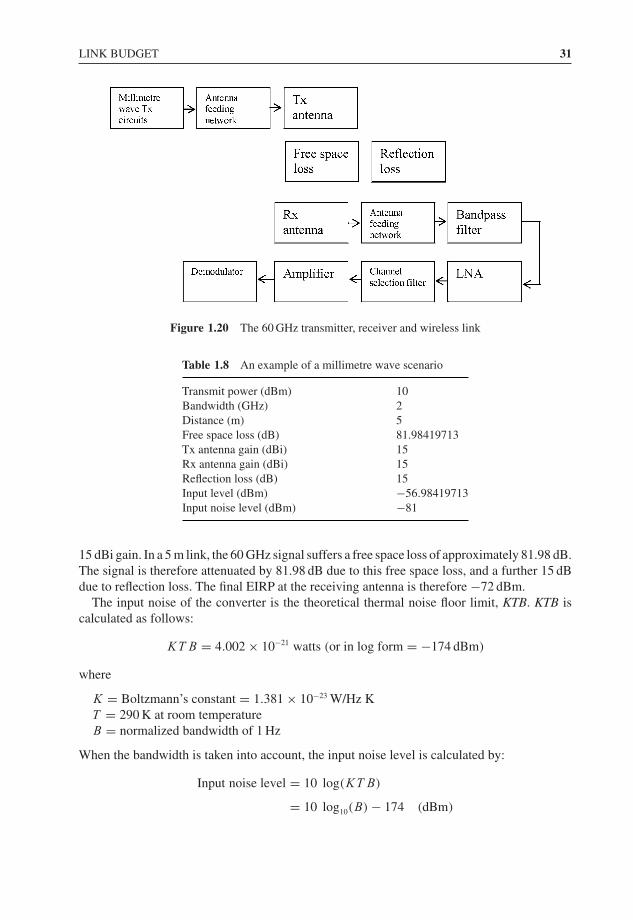
LINK BUDGET 31
Figure 1.20 The 60 GHz transmitter, receiver and wireless link
Table 1.8 An example of a millimetre wave scenario
Transmit power (dBm) 10Bandwidth (GHz) 2Distance (m) 5Free space loss (dB) 81.98419713Tx antenna gain (dBi) 15Rx antenna gain (dBi) 15Reflection loss (dB) 15Input level (dBm) −56.98419713Input noise level (dBm) −81
15 dBi gain. In a 5 m link, the 60 GHz signal suffers a free space loss of approximately 81.98 dB.The signal is therefore attenuated by 81.98 dB due to this free space loss, and a further 15 dBdue to reflection loss. The final EIRP at the receiving antenna is therefore −72 dBm.
The input noise of the converter is the theoretical thermal noise floor limit, KTB. KTB iscalculated as follows:
KT B = 4.002 × 10⁻²¹ watts (or in log form = −174 dBm)
where
K = Boltzmann’s constant = 1.381 × 10⁻²³ W/Hz KT = 290 K at room temperatureB = normalized bandwidth of 1 Hz
When the bandwidth is taken into account, the input noise level is calculated by:
Input noise level = 10 log(KT B)
= 10 log10(B) − 174 (dBm)
32 GIGABIT WIRELESS COMMUNICATIONS
where B = bandwidth (Hz). For a 2 GHz bandwidth, from the above, there is −81 dBm noiseat the receiver.
Table 1.8 is an example of a millimetre wave communication system link budget. Based onthis table, the signal-to-noise ratio of the system can be calculated.
Table 1.9 is an example of a cascaded millimetre wave receiver, which includes a feedingnetwork, a bandpass filter, a low-noise amplifier, a switch and channel selection filter, and anamplifier. The gain and noise figures for each component are provided, and the cumulativegain and noise figures are calculated.
Table 1.9 Components and their gain / noise figures
Feedingnetwork
Bandpassfilter
LNA Switch andchannelselection filter
Amplifier
Gain (dB) −5 −1 20 −5 30Cumulative
gain (dB)−5 −6 14 9 39
Cumulative gain(real)
0.31 0.25 25 7.94 7943
Noise figure (dB) 5 1 3 5 10Noise figure
(linear)3.16 1.26 2.00 3.16 10.00
Cumulative noisefigure (linear)
3.16 3.98 7.94 8.03 9.16
Cumulative noisefigure (dB)
5 6 9 9.04 9.62
A typical cascaded millimetre wave system is illustrated in Table 1.10. The transmit poweris assumed to be 10 dBm, and the loss for the feeding network for the transmitting antenna isassumed to be 5 dB. 15 dBm of power should be achieved before the signal enters the feedingnetwork. The transmitting antenna has a gain of 12 dBi, so the effective isotropic radiatedpower (e.i.r.p) increases to 22 dBm. During propagation, the signal undergoes free space lossand reflection loss, and so is reduced to −75 dBm.After the 12 dBi gain of the receiving antennaand the 5 dB loss of its feeding network, the signal increases to −68 dBm. Then the signal thenpasses through a filter with a −1 dB loss, a low-noise amplifier with a 20 dB gain (−43 dBm),a selection filter with a −5 dB loss (−48 dBm) and an amplifier with a 30 dB gain. Finally, thesignal power is −18 dBm.
The input noise level in Table 1.10 is stated as −81 dBm, as the bandwidth is assumed to be2 GHz. The noise then increases to −58 dBm due to a low-noise amplifier with a 3 dB noisefigure, which is then reduced to −63 dBm due to the selection filter with a 5 dB loss. Therefore,the signal-to-noise ratio at the output of the selection filter is (−54) − (−63) = 9 dB. Thepower level is plotted in Figure 1.21.
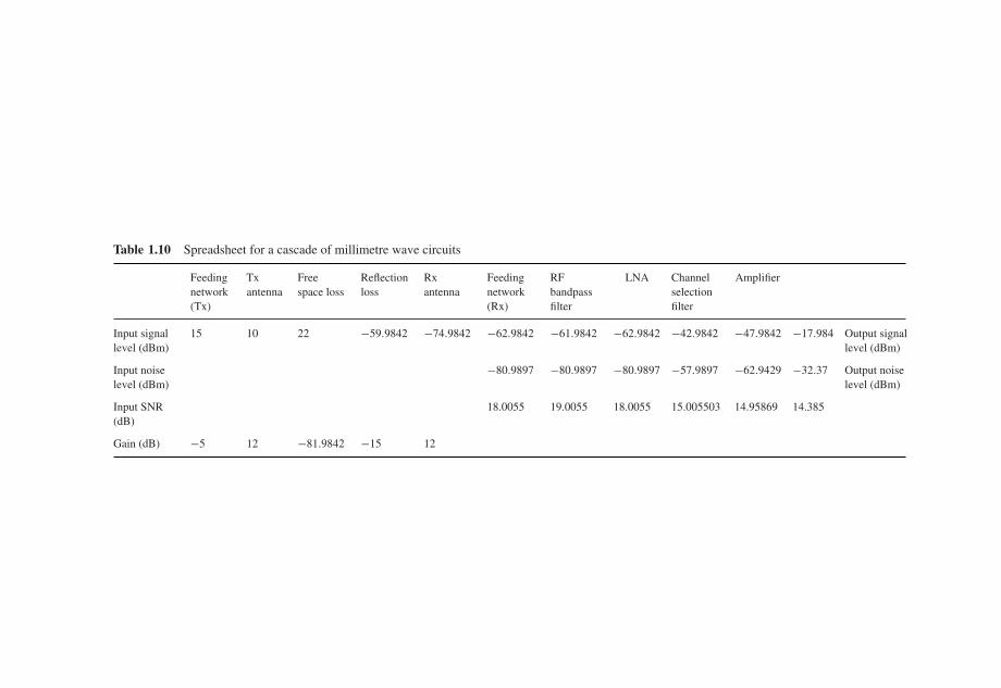
Table 1.10 Spreadsheet for a cascade of millimetre wave circuits
Feedingnetwork(Tx)
Txantenna
Freespace loss
Reflectionloss
Rxantenna
Feedingnetwork(Rx)
RFbandpassfilter
LNA Channelselectionfilter
Amplifier
Input signallevel (dBm)
15 10 22 −59.9842 −74.9842 −62.9842 −61.9842 −62.9842 −42.9842 −47.9842 −17.984 Output signallevel (dBm)
Input noiselevel (dBm)
−80.9897 −80.9897 −80.9897 −57.9897 −62.9429 −32.37 Output noiselevel (dBm)
Input SNR(dB)
18.0055 19.0055 18.0055 15.005503 14.95869 14.385
Gain (dB) −5 12 −81.9842 −15 12
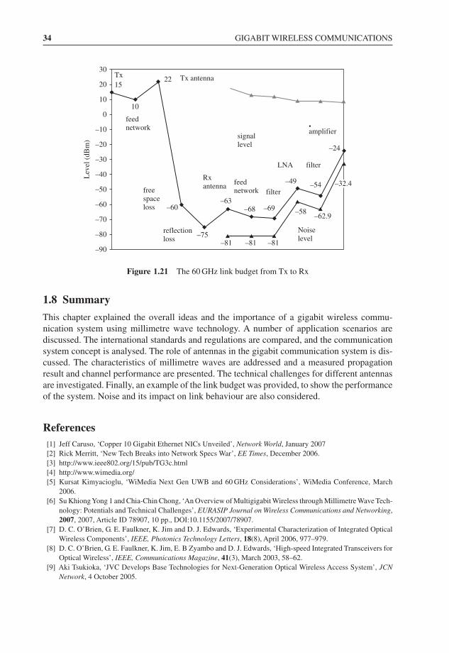
34 GIGABIT WIRELESS COMMUNICATIONS
Tx15
10
22 Tx antenna
feednetwork
signallevel
amplifier
–24
–49 –54
–58
–81–81
–68 –69–63
–60
–75–81
–62.9
filterLNA
Noiselevel
feednetwork filter
Rxantenna
reflectionloss
freespaceloss
–90
–80
–70
–60
–50
–40
–30
–20
–10
0
10
20
30
Lev
el (
dBm
)
–32.4
Figure 1.21 The 60 GHz link budget from Tx to Rx
1.8 Summary
This chapter explained the overall ideas and the importance of a gigabit wireless commu-nication system using millimetre wave technology. A number of application scenarios arediscussed. The international standards and regulations are compared, and the communicationsystem concept is analysed. The role of antennas in the gigabit communication system is dis-cussed. The characteristics of millimetre waves are addressed and a measured propagationresult and channel performance are presented. The technical challenges for different antennasare investigated. Finally, an example of the link budget was provided, to show the performanceof the system. Noise and its impact on link behaviour are also considered.
References[1] Jeff Caruso, ‘Copper 10 Gigabit Ethernet NICs Unveiled’, Network World, January 2007[2] Rick Merritt, ‘New Tech Breaks into Network Specs War’, EE Times, December 2006.[3] http://www.ieee802.org/15/pub/TG3c.html[4] http://www.wimedia.org/[5] Kursat Kimyacioglu, ‘WiMedia Next Gen UWB and 60 GHz Considerations’, WiMedia Conference, March
2006.[6] Su Khiong Yong 1 and Chia-Chin Chong, ‘An Overview of Multigigabit Wireless through Millimetre Wave Tech-
nology: Potentials and Technical Challenges’, EURASIP Journal on Wireless Communications and Networking,2007, 2007, Article ID 78907, 10 pp., DOI:10.1155/2007/78907.
[7] D. C. O’Brien, G. E. Faulkner, K. Jim and D. J. Edwards, ‘Experimental Characterization of Integrated OpticalWireless Components’, IEEE, Photonics Technology Letters, 18(8), April 2006, 977–979.
[8] D. C. O’Brien, G. E. Faulkner, K. Jim, E. B Zyambo and D. J. Edwards, ‘High-speed Integrated Transceivers forOptical Wireless’, IEEE, Communications Magazine, 41(3), March 2003, 58–62.
[9] Aki Tsukioka, ‘JVC Develops Base Technologies for Next-Generation Optical Wireless Access System’, JCNNetwork, 4 October 2005.

REFERENCES 35
[10] A. M. Street, P. N. Stavrinou, D. C. O’Brien and D. J. Edwards, ‘Indoor Optical Wireless Systems: A Review’,Optical and Quantum Electronics, 29(3), 1997, 349–378.
[11] D. C. O’Brien, E. B. Zyambo, G.. Faulkner, D. J. Edwards, D. M. Holburn, R. J. Mears, R. J. Samsudin,V. M. Joyner, V. A. Lalithambika, M. Whitehead, P. Stavrinou, G. Parry, J. Bellon and M J. Sibley, ‘High-SpeedOptical Wireless Transceivers for In-building Optical Local Area Networks (LANs)’, Conference on ‘OpticalWireless Communications III’, 4124, paper 4124-16, SPIE, Boston, Massachusetts, 2000.
[12] Kao-Cheng Huang and Zhaocheng Wang, ‘Millimetre-Wave Circular Polarized Beam-Steering Antenna Arrayfor Gigabit Wireless communications’, IEEE Transactions on Antennas and Propagation, 54(2), Part 2, February2006, 743–746.
[13] R. C. Qiu, H. Liu, X. Shen, ‘Ultra-wideband for Multiple Access Communications’, IEEE CommunicationsMagazine, 43(2), February 2005, 80–87.
[14] JVC Products, VIPSLAN OA-301, JVC Corporation Japan, http://www.jvc.co.jp/[15] Arturas Medeisis, ‘SE19 Drafting Group Meeting on MGWS at 60 GHz, ERO, Copenhagen, 26 March 2007’,
ERO SE19 Broadband Applications in Fixed Service, http://www.ero.dk/[16] European Radiocommunications Committee (ERC), T/R 22-03E, ‘Provisional Recommended Use of the
Frequency Range GHz by Terrestrial Fixed and Mobile Systems’, 1990, p. 3.[17] CEPT, ERO, ‘The European Table of Frequency Allocations,Locations and Utilisations Covering the Frequency
Range 9 kHz to 275 GHz’, Lisboa, January 2002; Dublin, 2003; Turkey, 2004; Copenhagen, 2004.[18] ERC Recommendation 12-09, ‘Radio Frequency Channel Arrangement for Fixed Service Systems Operating in
the Band 57.0–59.0 GHz Which Do Not Require Frequency Planning’, The Hague, 1998; revised Stockholm,October 2004.
[19] ECC Recommendation (05)02, ‘Use of the 64–66 GHz Frequency Band for Fixed Services’, June 2005.[20] ETSI DTR/ERM-RM-049, ‘Electromagnetic Compatibility and Radio Spectrum Matters (ERM); System Refer-
ence Document; Technical Characteristics of Multiple Gigabit Wireless Systems in the 60 GHz Range’, March2006.
[21] IEEE 802.15-15-06-0044-00-003c Document, ‘60 GHz Regulation in Germany’, January 2006.[22] Japan Regulations for Enforcement of the Radio Law 6-4-2 Specified Low Power Radio Station (11) 59–66 GHz
Band.[23] Ministry of Information Communication of Korea, ‘Frequency Allocation Comment of 60 GHz Band’, April
2006.[24] FCC, ‘Code of Federal Regulation, Title 47 Telecommunication’, Chapter 1, Part 15.255, October 2004.[25] Su Khiong Yong 1 and Chia-Chin Chong, ‘An Overview of Multigigabit Wireless through Millimetre Wave Tech-
nology: Potentials and Technical Challenges’, EURASIP Journal on Wireless Communications and Networking,2007, 2007, Article ID 78907, 10 pp.,DOI:10.1155/2007/78907
[26] Alireza Seyedi Philips, ‘Proposed European Regulations’, May 2006, IEEE 802.15-06-0247-00-003c.[27] Spectrum Management Telecommunications, ‘Radio Standard Specification-210, Issue 6, Low-Power License-
Exempt Radio Communication Devices (All Frequency Bands): Category 1 Equipment’, September 2005.[28] FCC document, OMB 3060-1070, ‘Allocations and Service Rules for the 71–76 GHz, 81–86 GHz, and
92–95 GHz Bands’.[29] Jonathan Wells, ‘Multigigabit Wireless Connectivity at 70, 80 and 90 GHz’, RF Design, May 2006, 50–54.[30] ERC Recommendation 12-09, ‘Radio Frequency Channel Arrangement for Fixed Service Systems Operating in
the Band 57.0–59.0 GHz Which Do Not Require Frequency Planning’, The Hague, 1998; revised Stockholm,October 2004.
[31] ARIB STD-T69, ‘Millimetre-Wave Video Transmission Equipment for Specified Low Power Radio Station’,July 2004.
[32] ARIB STD-T74, ‘Millimetre-Wave Data Transmission Equipment for Specified Low Power Radio Station (UltraHigh Speed Wireless LAN System)’, May 2001.
[33] http://www.ieee802.org/15/pub/TG3c.html[34] IEEE 802.15-05-0353-07-003c, ‘Working Group for Wireless Personal Area Networks (WPANs), TG3c System
Requirements’, January 2007.[35] H. T. Friis, ‘A Note on a Simple Transmission Formula’, Proceedings of the IRE, 34, 1946, 254–256.[36] M. Marcus and B. Pattan, ‘Millimetre Wave Propagation; Spectrum Management Implications’, IEEE Microwave
Magazine, 6(2), June 2005, 54–62.[37] David A. Sobel, ‘60 GHz Wireless System Design: Towards a 1Gb/s wireless link’, Research Retreat at Berkeley
Wireless Research Centre, June 2003.

36 GIGABIT WIRELESS COMMUNICATIONS
[38] David A. Sobel and Robert W. Brodersen, ‘60GHz CMOS System Design: Challenges, Opportunities, and NextSteps’, Research Retreat at Berkeley Wireless Research Centre, January 2003.
[39] M. K. Simon and M. S. Alouini, ‘Digital Communication over Fading Channels’, 2nd edition, Wiley-IEEE Press,New York, 2004.
[40] Katsuyoshi Sato, Takeshi Manabe, Toshio Ihara, Hiroshi Saito, Shigeru Ito, Tetsu Tanaka, Kazuyoshi Sugai,Norichika Ohmi, Yasushi Murakami, Masanori Shibayama, Yoshihiko Konishi and Tsuneto Kimura, ‘Measure-ments of Reflection and Transmission Characteristics of Interior Structures of Office Building in the 60-GHzBand’, IEEE Transactions on Antennas and Propagation, 45(12), December 1997, 1783–1792.
[41] Chinh H. Doan, Sohrab Emami, David A. Sobel, Ali M. Niknejad and Robert W. Brodersen, ‘DesignConsiderations for 60 GHz CMOS Radios’, IEEE Communications Magazine, December 2004, 132–140.
[42] M. R. Williamson, G. E.Athanasiadou andA. R. Nix, ‘Investigating the Effects ofAntenna Directivity on WirelessIndoor Communication at 60 GHz’, 8th IEEE International Symposium PIMRC, September 1997, pp. 635–639.
[43] R. C. Hansen, ‘Phased Array Antennas’, Wiley-Interscience, 19 January 1998.[44] A. Abidi, ‘Direct Conversion Radio Transceivers for Digital Communications’, IEEE JSSSC, 30(12), 1995,
1399–1410.[45] F. Aschwanden, ‘Direct Conversion – How to Make It Work in TV Tuners’, IEEE Transactions on Consumer
Electronics, 42(3), August 1996, 729–751.[46] J. Wenin, ‘ICS for Digital Cellular Communication’, European Solid State Circuits Conference, Ulm, Germany,
1994, pp. 1–10.[47] Y. Zhao, C. Viereck, J. F. Frigon, R. G. Bosisio and K. Wu, ‘Direct Quadrature Phase Shift Keying Modulator
Using Sixport Technology’, Electronics Letters, 41(21), 2005, 1180–1181.[48] R. G. Vaughan, N. Scott and D. White, ‘The Theory of Bandpass Sampling’, IEEE Transactions on Signal
Processing, 39(9), September 1991, 1973–1984.[49] C. A. Balanis, ‘Antenna Theory: Analysis and Design’, 2nd edition, John Wiley & Sons, Inc., New York, 1997.[50] K.-C. Huang and Z. Wang, ‘Millimetre-Wave Circular Polarized Beam-Steering Antenna Array for Gigabit
Wireless Communications’, IEEE Transactions on Antennas and Propagation, 54(2), Part 2, 2006, 743–746,DOI:10.1109/TAP.2005.863158.
[51] J.-Y. Park, Y. Wang and T. Itoh, ‘A 60 GHz Integrated Antenna Array for High-Speed Digital BeamformingApplications’, in Proceedings of IEEE MTT-S International Microwave Symposium Digest, Vol. 3, Philadelphia,Pennsylvania, June 2003, pp. 1677–1680.
[52] K. Huang and S. Koch, ‘Circular Polarization Antenna’, European Patent EP1564843.[53] K. Huang and Z. Wang, ‘Dielectric Rod Antenna and Method for Operating the Antenna’, World Patent
WO2006097145; European Patent EP1703590.[54] IEEE 802.15-05-0493-27-003c, ‘TG3c Selection Criteria’, January 2007.
2Critical Antenna Parameters
Based on the discussion in Chapter 1, the descriptions and requirements are developed, forthe system components of a (nominally) 60 GHz free space point-to-point communicationssystem. Also to be taken into consideration for this technology are user-defined constraints(such as size and bulk) and these will dictate or steer the direction of the design philosophy.There are five main constraints that will be explored for millimetre wave antenna design.
The first constraint is that the 60 GHz channel is lossy (due to oxygen absorption) but isotherwise benign. The excess loss at 60 GHz is approximately 15 dB/km and it is thereforedesirable to identify means to overcome oxygen absorption and ensure that a sufficient mar-gin exists to overcome other losses, such as rain-induced fading. Here compensation can beacheived by increasing the transmitter or receiver antenna gain. For example, a directionalantenna gain can be employed to substitute for raw transmitter power and receiver noise. Thusthere is the prospect of system optimisation by trading off the requirements in these differentareas, and this aspect will be considered in Section 2.1.
The second constraint for systems is a strong multipath effect in an indoor environment.In other words, the line-of-sight signal and the reflected signal will arrive at the receivervia different paths. When the path difference is n×λ/2(n = 1, 3, . . .), there is a destructiveinterference between signals and this causes a notch in the frequency spectrum. For example,if the path difference is 2.5 mm, there will be a notch at 60 GHz and such a notch can causean unstable wireless link with only slight physical displacement of the terminals or scatterers;this will reduce the quality of the communications link. To minimise the multipath effect, anarrow-beam antenna is therefore preferred. A discussion of the optimisation of the beamwidthis given in Section 2.2.
The third constraint is the space limit for portable devices such as handsets. It is essentialto know how much gain can be achieved for an antenna in such a restricted space limit. Thislimit will be discussed in Section 2.3. For a predominantly line-of-sight wireless link, circularpolarisation is useful to filter out the first reflected (multipath) signal. Additionally, the wirelesscommunication data rate (the capacity of the link) can be increased by using multipolarisa-tion in a multitransmitter–multireceiver system. Each polarization state can deliver differentinformation channels and thus the data rate will be increased two to three times. Conversely, ifthe major concern is the robustness of the link, the question of frequency re-use by polarisation
Millimetre Wave Antennas for Gigabit Wireless Communications Kao-Cheng Huang and David J. Edwardsc© 2008 John Wiley & Sons, Ltd
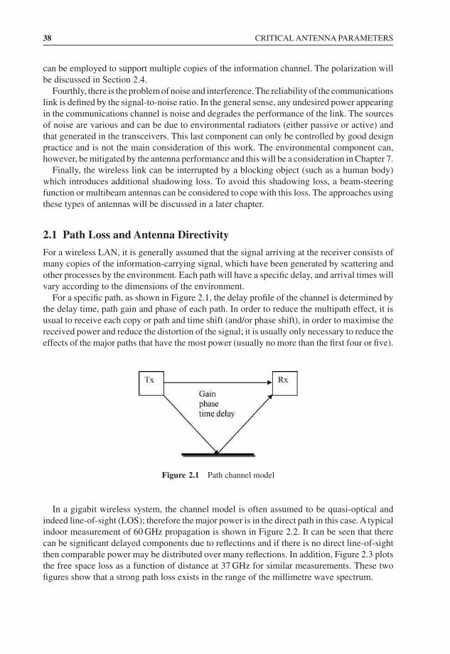
38 CRITICAL ANTENNA PARAMETERS
can be employed to support multiple copies of the information channel. The polarization willbe discussed in Section 2.4.
Fourthly, there is the problem of noise and interference.The reliability of the communicationslink is defined by the signal-to-noise ratio. In the general sense, any undesired power appearingin the communications channel is noise and degrades the performance of the link. The sourcesof noise are various and can be due to environmental radiators (either passive or active) andthat generated in the transceivers. This last component can only be controlled by good designpractice and is not the main consideration of this work. The environmental component can,however, be mitigated by the antenna performance and this will be a consideration in Chapter 7.
Finally, the wireless link can be interrupted by a blocking object (such as a human body)which introduces additional shadowing loss. To avoid this shadowing loss, a beam-steeringfunction or multibeam antennas can be considered to cope with this loss. The approaches usingthese types of antennas will be discussed in a later chapter.
2.1 Path Loss and Antenna Directivity
For a wireless LAN, it is generally assumed that the signal arriving at the receiver consists ofmany copies of the information-carrying signal, which have been generated by scattering andother processes by the environment. Each path will have a specific delay, and arrival times willvary according to the dimensions of the environment.
For a specific path, as shown in Figure 2.1, the delay profile of the channel is determined bythe delay time, path gain and phase of each path. In order to reduce the multipath effect, it isusual to receive each copy or path and time shift (and/or phase shift), in order to maximise thereceived power and reduce the distortion of the signal; it is usually only necessary to reduce theeffects of the major paths that have the most power (usually no more than the first four or five).
Figure 2.1 Path channel model
In a gigabit wireless system, the channel model is often assumed to be quasi-optical andindeed line-of-sight (LOS); therefore the major power is in the direct path in this case. A typicalindoor measurement of 60 GHz propagation is shown in Figure 2.2. It can be seen that therecan be significant delayed components due to reflections and if there is no direct line-of-sightthen comparable power may be distributed over many reflections. In addition, Figure 2.3 plotsthe free space loss as a function of distance at 37 GHz for similar measurements. These twofigures show that a strong path loss exists in the range of the millimetre wave spectrum.
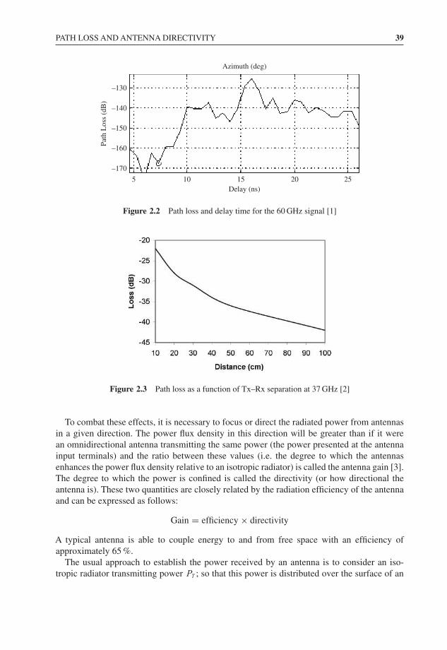
PATH LOSS AND ANTENNA DIRECTIVITY 39
5
–170
–160
–150
–140
–130
10 15 20 25Delay (ns)
Azimuth (deg)
Path
Los
s (d
B)
Figure 2.2 Path loss and delay time for the 60 GHz signal [1]
Figure 2.3 Path loss as a function of Tx–Rx separation at 37 GHz [2]
To combat these effects, it is necessary to focus or direct the radiated power from antennasin a given direction. The power flux density in this direction will be greater than if it werean omnidirectional antenna transmitting the same power (the power presented at the antennainput terminals) and the ratio between these values (i.e. the degree to which the antennasenhances the power flux density relative to an isotropic radiator) is called the antenna gain [3].The degree to which the power is confined is called the directivity (or how directional theantenna is). These two quantities are closely related by the radiation efficiency of the antennaand can be expressed as follows:
Gain = efficiency × directivity
A typical antenna is able to couple energy to and from free space with an efficiency ofapproximately 65 %.
The usual approach to establish the power received by an antenna is to consider an iso-tropic radiator transmitting power PT ; so that this power is distributed over the surface of an
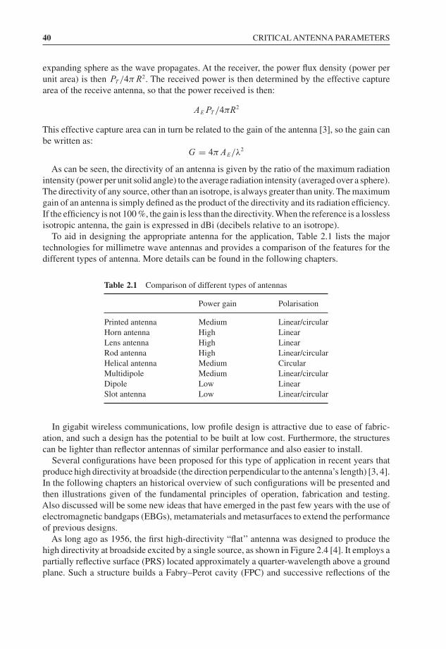
40 CRITICAL ANTENNA PARAMETERS
expanding sphere as the wave propagates. At the receiver, the power flux density (power perunit area) is then PT /4πR2. The received power is then determined by the effective capturearea of the receive antenna, so that the power received is then:
AEPT /4πR2
This effective capture area can in turn be related to the gain of the antenna [3], so the gain canbe written as:
G = 4πAE/λ2
As can be seen, the directivity of an antenna is given by the ratio of the maximum radiationintensity (power per unit solid angle) to the average radiation intensity (averaged over a sphere).The directivity of any source, other than an isotrope, is always greater than unity. The maximumgain of an antenna is simply defined as the product of the directivity and its radiation efficiency.If the efficiency is not 100 %, the gain is less than the directivity. When the reference is a losslessisotropic antenna, the gain is expressed in dBi (decibels relative to an isotrope).
To aid in designing the appropriate antenna for the application, Table 2.1 lists the majortechnologies for millimetre wave antennas and provides a comparison of the features for thedifferent types of antenna. More details can be found in the following chapters.
Table 2.1 Comparison of different types of antennas
Power gain Polarisation
Printed antenna Medium Linear/circularHorn antenna High LinearLens antenna High LinearRod antenna High Linear/circularHelical antenna Medium CircularMultidipole Medium Linear/circularDipole Low LinearSlot antenna Low Linear/circular
In gigabit wireless communications, low profile design is attractive due to ease of fabric-ation, and such a design has the potential to be built at low cost. Furthermore, the structurescan be lighter than reflector antennas of similar performance and also easier to install.
Several configurations have been proposed for this type of application in recent years thatproduce high directivity at broadside (the direction perpendicular to the antenna’s length) [3, 4].In the following chapters an historical overview of such configurations will be presented andthen illustrations given of the fundamental principles of operation, fabrication and testing.Also discussed will be some new ideas that have emerged in the past few years with the use ofelectromagnetic bandgaps (EBGs), metamaterials and metasurfaces to extend the performanceof previous designs.
As long ago as 1956, the first high-directivity “flat’’ antenna was designed to produce thehigh directivity at broadside excited by a single source, as shown in Figure 2.4 [4]. It employs apartially reflective surface (PRS) located approximately a quarter-wavelength above a groundplane. Such a structure builds a Fabry–Perot cavity (FPC) and successive reflections of the
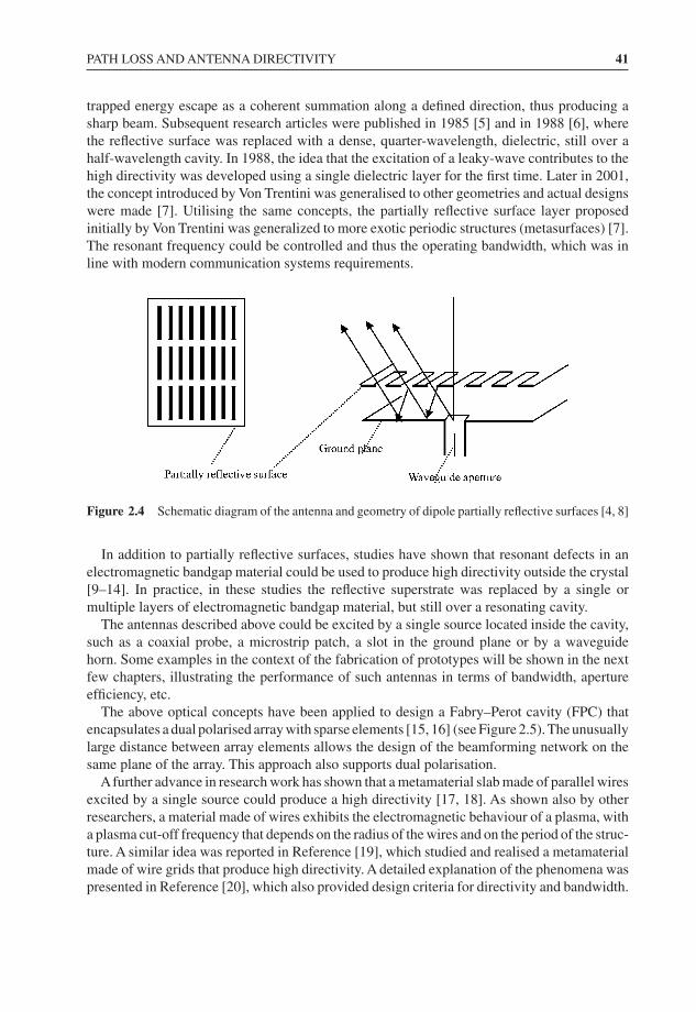
PATH LOSS AND ANTENNA DIRECTIVITY 41
trapped energy escape as a coherent summation along a defined direction, thus producing asharp beam. Subsequent research articles were published in 1985 [5] and in 1988 [6], wherethe reflective surface was replaced with a dense, quarter-wavelength, dielectric, still over ahalf-wavelength cavity. In 1988, the idea that the excitation of a leaky-wave contributes to thehigh directivity was developed using a single dielectric layer for the first time. Later in 2001,the concept introduced by Von Trentini was generalised to other geometries and actual designswere made [7]. Utilising the same concepts, the partially reflective surface layer proposedinitially by Von Trentini was generalized to more exotic periodic structures (metasurfaces) [7].The resonant frequency could be controlled and thus the operating bandwidth, which was inline with modern communication systems requirements.
Figure 2.4 Schematic diagram of the antenna and geometry of dipole partially reflective surfaces [4, 8]
In addition to partially reflective surfaces, studies have shown that resonant defects in anelectromagnetic bandgap material could be used to produce high directivity outside the crystal[9–14]. In practice, in these studies the reflective superstrate was replaced by a single ormultiple layers of electromagnetic bandgap material, but still over a resonating cavity.
The antennas described above could be excited by a single source located inside the cavity,such as a coaxial probe, a microstrip patch, a slot in the ground plane or by a waveguidehorn. Some examples in the context of the fabrication of prototypes will be shown in the nextfew chapters, illustrating the performance of such antennas in terms of bandwidth, apertureefficiency, etc.
The above optical concepts have been applied to design a Fabry–Perot cavity (FPC) thatencapsulates a dual polarised array with sparse elements [15, 16] (see Figure 2.5).The unusuallylarge distance between array elements allows the design of the beamforming network on thesame plane of the array. This approach also supports dual polarisation.
Afurther advance in research work has shown that a metamaterial slab made of parallel wiresexcited by a single source could produce a high directivity [17, 18]. As shown also by otherresearchers, a material made of wires exhibits the electromagnetic behaviour of a plasma, witha plasma cut-off frequency that depends on the radius of the wires and on the period of the struc-ture. A similar idea was reported in Reference [19], which studied and realised a metamaterialmade of wire grids that produce high directivity. A detailed explanation of the phenomena waspresented in Reference [20], which also provided design criteria for directivity and bandwidth.
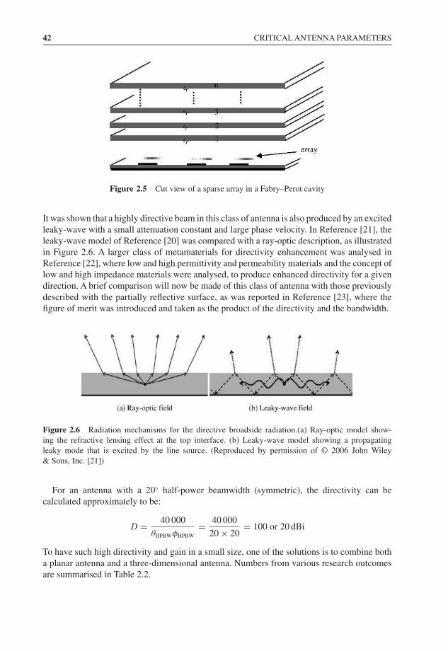
42 CRITICAL ANTENNA PARAMETERS
Figure 2.5 Cut view of a sparse array in a Fabry–Perot cavity
It was shown that a highly directive beam in this class of antenna is also produced by an excitedleaky-wave with a small attenuation constant and large phase velocity. In Reference [21], theleaky-wave model of Reference [20] was compared with a ray-optic description, as illustratedin Figure 2.6. A larger class of metamaterials for directivity enhancement was analysed inReference [22], where low and high permittivity and permeability materials and the concept oflow and high impedance materials were analysed, to produce enhanced directivity for a givendirection. A brief comparison will now be made of this class of antenna with those previouslydescribed with the partially reflective surface, as was reported in Reference [23], where thefigure of merit was introduced and taken as the product of the directivity and the bandwidth.
Figure 2.6 Radiation mechanisms for the directive broadside radiation.(a) Ray-optic model show-ing the refractive lensing effect at the top interface. (b) Leaky-wave model showing a propagatingleaky mode that is excited by the line source. (Reproduced by permission of © 2006 John Wiley& Sons, Inc. [21])
For an antenna with a 20◦ half-power beamwidth (symmetric), the directivity can becalculated approximately to be:
D = 40 000
θHPBWφHPBW
= 40 000
20 × 20= 100 or 20 dBi
To have such high directivity and gain in a small size, one of the solutions is to combine botha planar antenna and a three-dimensional antenna. Numbers from various research outcomesare summarised in Table 2.2.
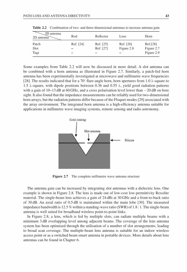
PATH LOSS AND ANTENNA DIRECTIVITY 43
Table 2.2 Combination of two- and three-dimensional antennas to increase antenna gain
2D antenna3D antenna
Rod Reflector Lens Horn
Patch Ref. [24] Ref. [25] Ref. [26] Ref.[28]Slot – Ref. [27] Figure 2.8 Figure 2.7Yagi – – – Figure 2.9
Some examples from Table 2.2 will now be discussed in more detail. A slot antenna canbe combined with a horn antenna as illustrated in Figure 2.7. Similarly, a patch-fed hornantenna has been experimentally investigated at microwave and millimetre wave frequencies[28]. The results indicated that for a 70◦ flare-angle horn, horn apertures from 1.0 λ-square to1.5 λ-square, with dipole positions between 0.36 and 0.55 λ, yield good radiation patternswith a gain of 10–13 dB at 60 GHz, and a cross polarisation level lower than −20 dB on boresight. It also found that the impedance measurements can be reliably used for two-dimensionalhorn arrays, but the radiation patterns differ because of the Floquet modes [29] associated withthe array environment. The integrated horn antenna is a high-efficiency antenna suitable forapplications in millimetre wave imaging systems, remote sensing and radio astronomy.
Figure 2.7 The complete millimetre wave antenna structure
The antenna gain can be increased by integrating slot antennas with a dielectric lens. Oneexample is shown in Figure 2.8. The lens is made out of low-cost low-permittivity Rexolitematerial. The single-beam lens achieves a gain of 24 dBi at 30 GHz and a front-to-back ratioof 30 dB. An axial ratio of 0.5 dB is maintained within the main lobe [30]. The measuredimpedance bandwidth is 12.5 % within a standing-wave ratio (SWR) of 1.8 : 1. The single-beamantenna is well suited for broadband wireless point-to-point links.
In Figure 2.8, a lens, which is fed by multiple slots, can radiate multiple beams with aminimum 3 dB overlapping level among adjacent beams. The coverage of the lens antennasystem has been optimised through the utilisation of a number of slot arrangements, leadingto broad scan coverage. The multiple-beam lens antenna is suitable for an indoor wirelessaccess point or as a switched beam smart antenna in portable devices. More details about lensantennas can be found in Chapter 6.
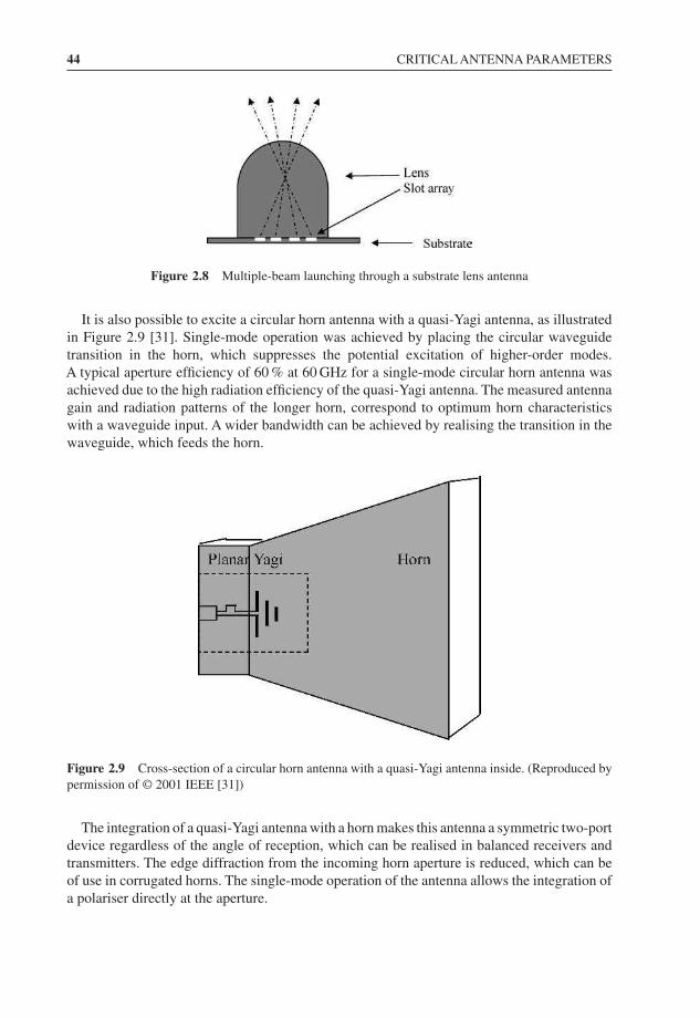
44 CRITICAL ANTENNA PARAMETERS
Figure 2.8 Multiple-beam launching through a substrate lens antenna
It is also possible to excite a circular horn antenna with a quasi-Yagi antenna, as illustratedin Figure 2.9 [31]. Single-mode operation was achieved by placing the circular waveguidetransition in the horn, which suppresses the potential excitation of higher-order modes.A typical aperture efficiency of 60 % at 60 GHz for a single-mode circular horn antenna wasachieved due to the high radiation efficiency of the quasi-Yagi antenna. The measured antennagain and radiation patterns of the longer horn, correspond to optimum horn characteristicswith a waveguide input. A wider bandwidth can be achieved by realising the transition in thewaveguide, which feeds the horn.
Figure 2.9 Cross-section of a circular horn antenna with a quasi-Yagi antenna inside. (Reproduced bypermission of © 2001 IEEE [31])
The integration of a quasi-Yagi antenna with a horn makes this antenna a symmetric two-portdevice regardless of the angle of reception, which can be realised in balanced receivers andtransmitters. The edge diffraction from the incoming horn aperture is reduced, which can beof use in corrugated horns. The single-mode operation of the antenna allows the integration ofa polariser directly at the aperture.
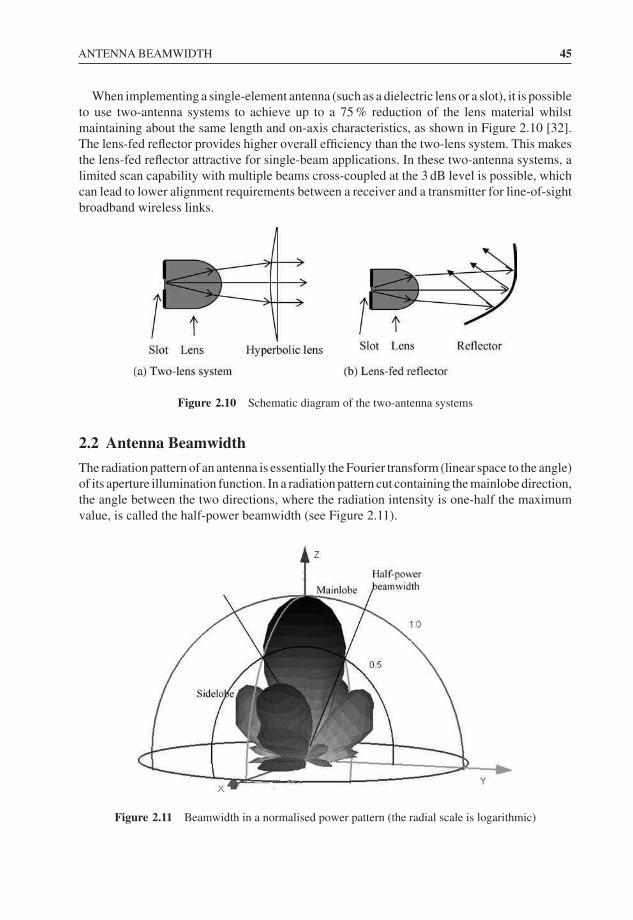
ANTENNA BEAMWIDTH 45
When implementing a single-element antenna (such as a dielectric lens or a slot), it is possibleto use two-antenna systems to achieve up to a 75 % reduction of the lens material whilstmaintaining about the same length and on-axis characteristics, as shown in Figure 2.10 [32].The lens-fed reflector provides higher overall efficiency than the two-lens system. This makesthe lens-fed reflector attractive for single-beam applications. In these two-antenna systems, alimited scan capability with multiple beams cross-coupled at the 3 dB level is possible, whichcan lead to lower alignment requirements between a receiver and a transmitter for line-of-sightbroadband wireless links.
Figure 2.10 Schematic diagram of the two-antenna systems
2.2 Antenna Beamwidth
The radiation pattern of an antenna is essentially the Fourier transform (linear space to the angle)of its aperture illumination function. In a radiation pattern cut containing the mainlobe direction,the angle between the two directions, where the radiation intensity is one-half the maximumvalue, is called the half-power beamwidth (see Figure 2.11).
Figure 2.11 Beamwidth in a normalised power pattern (the radial scale is logarithmic)
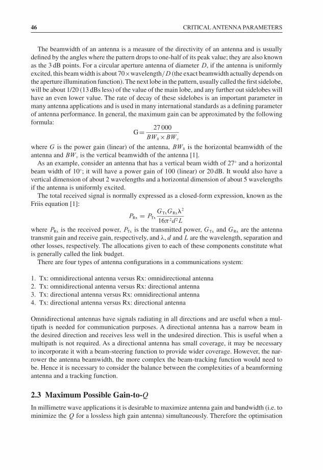
46 CRITICAL ANTENNA PARAMETERS
The beamwidth of an antenna is a measure of the directivity of an antenna and is usuallydefined by the angles where the pattern drops to one-half of its peak value; they are also knownas the 3 dB points. For a circular aperture antenna of diameter D, if the antenna is uniformlyexcited, this beam width is about 70×wavelength/D (the exact beamwidth actually depends onthe aperture illumination function). The next lobe in the pattern, usually called the first sidelobe,will be about 1/20 (13 dBs less) of the value of the main lobe, and any further out sidelobes willhave an even lower value. The rate of decay of these sidelobes is an important parameter inmany antenna applications and is used in many international standards as a defining parameterof antenna performance. In general, the maximum gain can be approximated by the followingformula:
G= 27 000
BWh×BWv
where G is the power gain (linear) of the antenna, BWh is the horizontal beamwidth of theantenna and BWv is the vertical beamwidth of the antenna [1].
As an example, consider an antenna that has a vertical beam width of 27◦ and a horizontalbeam width of 10◦; it will have a power gain of 100 (linear) or 20 dB. It would also have avertical dimension of about 2 wavelengths and a horizontal dimension of about 5 wavelengthsif the antenna is uniformly excited.
The total received signal is normally expressed as a closed-form expression, known as theFriis equation [1]:
PRx = PTx
GTxGRx�2
16π 2d2L
where PRx is the received power, PTx is the transmitted power, GTx and GRx are the antennatransmit gain and receive gain, respectively, and λ, d and L are the wavelength, separation andother losses, respectively. The allocations given to each of these components constitute whatis generally called the link budget.
There are four types of antenna configurations in a communications system:
1. Tx: omnidirectional antenna versus Rx: omnidirectional antenna2. Tx: omnidirectional antenna versus Rx: directional antenna3. Tx: directional antenna versus Rx: omnidirectional antenna4. Tx: directional antenna versus Rx: directional antenna
Omnidirectional antennas have signals radiating in all directions and are useful when a mul-tipath is needed for communication purposes. A directional antenna has a narrow beam inthe desired direction and receives less well in the undesired direction. This is useful when amultipath is not required. As a directional antenna has small coverage, it may be necessaryto incorporate it with a beam-steering function to provide wider coverage. However, the nar-rower the antenna beamwidth, the more complex the beam-tracking function would need tobe. Hence it is necessary to consider the balance between the complexities of a beamformingantenna and a tracking function.
2.3 Maximum Possible Gain-to-Q
In millimetre wave applications it is desirable to maximize antenna gain and bandwidth (i.e. tominimize the Q for a lossless high gain antenna) simultaneously. Therefore the optimisation
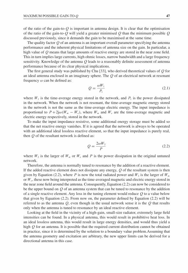
MAXIMUM POSSIBLE GAIN-TO-Q 47
of the ratio of the gain-to-Q is important in antenna design. It is clear that the optimisationof the ratio of the gain-to-Q will yield a greater minimised Q than the minimum possible Q
discussed previously, since it demands the gain to be maximised at the same time.The quality factor Q of an antenna is an important overall parameter specifying the antenna
performance and the inherent physical limitations of antenna size on the gain. In particular, ahigh value of Q means that large amounts of reactive energy are stored in the near zone field.This in turn implies large currents, high ohmic losses, narrow bandwidth and a large frequencysensitivity. Knowledge of the antenna Q leads to a reasonably definite assessment of antennaperformance because of its clear physical implications.
The first general study was published by Chu [33], who derived theoretical values of Q foran ideal antenna enclosed in an imaginary sphere. The Q of an electrical network at resonantfrequency ω can be defined as:
Q = ωW1
P1
(2.1)
where W1 is the time-average energy stored in the network, and P1 is the power dissipatedin the network. When the network is not resonant, the time-average magnetic energy storedin the network is not the same as the time-average electric energy. The input impedance isproportional to P +2jω(Wm − We), where Wm and We are the time-average magnetic andelectric energy respectively, stored in the network.
To make the input impedance resistive, some additional energy storage must be added sothat the net reactive energy vanishes. If it is agreed that the network is always to be operatedwith an additional ideal lossless reactive element, so that the input impedance is purely real,then Q of the resultant network is defined as:
Q = 2ωW2
P(2.2)
where W2 is the larger of Wm or We and P is the power dissipation in the original untunednetwork.
Therefore, the antenna is normally tuned to resonance by the addition of a reactive element.If the added reactive element does not dissipate any energy, Q of the resultant system is thengiven by Equation (2.2), where P is now the total radiated power and W2 is the larger of Wm
or We, these now being interpreted as the time-averaged magnetic and electric energy stored inthe near zone field around the antenna. Consequently, Equation (2.2) can now be considered tobe the upper bound on Q of an antenna system that can be tuned to resonance by the additionof a single reactive element. Any loss in the tuning element would reduce Q to a value belowthat given by Equation (2.2). From now on, the parameter defined by Equation (2.2) will bereferred to as the antenna Q, even though in the usual network sense it is the Q that resultsonly when the antenna is tuned to resonance by an ideal reactive element.
Looking at the field in the vicinity of a high-gain, small-size radiator, extremely large fieldintensities can be found. In a physical antenna, this would result in prohibitive heat loss. Inan ideal lossless antenna, this would result in large energy densities, and would thus yield ahigh Q for an antenna. It is possible that the required current distribution cannot be obtainedin practice, since it is determined by the solution to a boundary value problem.Assuming thatthe antenna geometry and excitation are arbitrary, the new upper limits can be derived for adirectional antenna in this case.
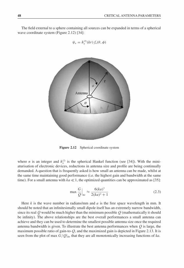
48 CRITICAL ANTENNA PARAMETERS
The field external to a sphere containing all sources can be expanded in terms of a sphericalwave coordinate system (Figure 2.12) [34]:
ψn = h(2)
n(kr)fn(θ, φ)
Figure 2.12 Spherical coordinate system
where n is an integer and h(2)n
is the spherical Hankel function (see [34]). With the mini-aturisation of electronic devices, reductions in antenna size and profile are being continuallydemanded. A question that is frequently asked is how small an antenna can be made, whilst atthe same time maintaining good performance (i.e. the highest gain and bandwidth at the sametime). For a small antenna with ka �1, the optimized quantities can be approximated as [35]:
maxG
Q
∣∣∣dir
≈ 6(ka)3
2(ka)2 + 1(2.3)
Here k is the wave number in radians/mm and a is the free space wavelength in mm. Itshould be noted that an infinitesimally small dipole itself has an extremely narrow bandwidth,since its real Q would be much higher than the minimum possible Q (mathematically it shouldbe infinity). The above relationships are the best overall performances a small antenna canachieve and they can be used to determine the smallest possible antenna size once the requiredantenna bandwidth is given. To illustrate the best antenna performances when Q is large, themaximum possible ratio of gain-to-Q, and the maximized gain is depicted in Figure 2.13. It isseen from the plot of max G/Q|dir that they are all monotonically increasing functions of ka.
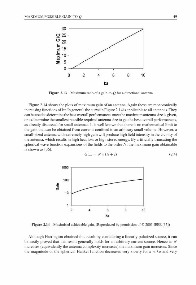
MAXIMUM POSSIBLE GAIN-TO-Q 49
Figure 2.13 Maximum ratio of a gain-to-Q for a directional antenna
Figure 2.14 shows the plots of maximum gain of an antenna. Again these are monotonicallyincreasing functions of ka. In general, the curve in Figure 2.14 is applicable to all antennas. Theycan be used to determine the best overall performances once the maximum antenna size is given,or to determine the smallest possible required antenna size to get the best overall performances,as already discussed for small antennas. It is well known that there is no mathematical limit tothe gain that can be obtained from currents confined to an arbitrary small volume. However, asmall-sized antenna with extremely high gain will produce high field intensity in the vicinity ofthe antenna, which results in high heat loss or high stored energy. By artificially truncating thespherical wave function expansions of the fields to the order N , the maximum gain obtainableis shown as [36]:
Gmax = N ×(N +2) (2.4)
Figure 2.14 Maximised achievable gain. (Reproduced by permission of © 2003 IEEE [35])
Although Harrington obtained this result by considering a linearly polarized source, it canbe easily proved that this result generally holds for an arbitrary current source. Hence as N
increases (equivalently the antenna complexity increases) the maximum gain increases. Sincethe magnitude of the spherical Hankel function decreases very slowly for n < ka and very
50 CRITICAL ANTENNA PARAMETERS
rapidly for n>ka, the approximate transition point ka = n can be considered to be the pointof gradual cut-off [37].
The normal gain is often introduced and defined by letting N =ka [33, 36, 38], so Gnorm =ka×(ka+2).Any antenna having a larger gain than the normal gain has been called a supergainantenna. It is believed that using a supergain antenna will result in a high Q and is therefore notvery practical, and so the normal gain is the maximum gain achievable without incurring highQ. The plot of Gnorm is shown in Figure 2.14. It is clear that the definition of the normal gainor supergain is ambiguous since the cut-off point n=ka is an approximate transition point andin addition, Q is not clearly specified.
Assuming there is an infinite ground plane and the sphere has a radius which can enclose theantenna, and a =5 mm, the free space wavelength at 60 GHz can be calculated and the wavenumber that allows ka to be evaluated:
� = c
f= 3 × 108 × 103
60 × 109= 5 mm
k = 2π
�= 1.26 radians/mm
Therefore:
ka = 1.26×5 = 6.3
From Equations (2.3) and (2.4), the maximum gain-to-Q factor and maximum gainis given as:
maxG
Q
∣∣∣∣dir
≈ 6(6.3)3
2(6.3)2 + 1= 18.7
Maximum gain = 6.3(6.3 + 2) = 52.3 = 17 dB
2.4 Antenna Polarisation
The subject of antenna polarisation has generated much published material over the years. Theprecise definition can be complex, and radiating and receiving structures respond varyingly,both in frequency and the angle to incident and transmitted waves. Here the discussion shallbe confined to a simple treatment, and the reader is directed to texts that deal with the topicin much greater depth [1]. Only “far-field’’ radiation will be considered (since the wavelengthis small compared with the dimensions of the radiators) and for the illustive cases presentedhere plane wave propagation will also be assumed.
In free space, the energy radiated by any antenna is carried by a transverse electromagneticwave, that is comprised of an electric and a magnetic field. These fields are orthogonal to eachanother and also orthogonal to the direction of propagation. The electric field of the electro-magnetic wave is used to define the polarisation plane of the wave, and therefore describes thepolarisation state of the antenna.
For describing antenna polarisation properties the “Ludwig definition 3’’ is commonly used[37]. In this definition, reference and cross polarisations are defined as the measurementobtained when antenna patterns are taken in the usual manner, as illustrated in Figure 2.15.
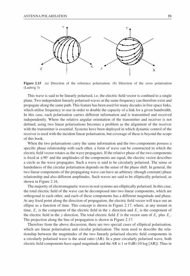
ANTENNA POLARISATION 51
Figure 2.15 (a) Direction of the reference polarisation. (b) Direction of the cross polarisation(Ludwig 3)
This wave is said to be linearly polarised, i.e. the electric field vector is confined to a singleplane. Two independent linearly polarised waves at the same frequency can therefore exist andpropagate along the same path. This feature has been used for many decades in free space links,which utilise frequency re-use in order to double the capacity of a link for a given bandwidth.In this case, each polarisation carries different information and is transmitted and receivedindependently. Where the relative angular orientation of the transmitter and receiver is notdefined, using two linear polarisations becomes a problem as the alignment of the receiverwith the transmitter is essential. Systems have been deployed in which dynamic control of thereceiver is used with the incident linear polarisation, but coverage of these is beyond the scopeof this book.
When the two polarisations carry the same information and the two components possess aspecific phase relationship with each other, a form of wave can be constructed in which theelectric field vector rotates as the wave propagates. If the relative phase of the two componentsis fixed at ±90◦ and the amplitudes of the components are equal, the electric vector describesa circle as the wave propagates. Such a wave is said to be circularly polarised. The sense orhandedness of the circular polarisation depends on the sense of the phase shift. In general, thetwo linear components of the propagating wave can have an arbitrary (though constant) phaserelationship and also different amplitudes. Such waves are said to be elliptically polarised, asshown in Figure 2.16.
The majority of electromagnetic waves in real systems are elliptically polarised. In this case,the total electric field of the wave can be decomposed into two linear components, which areorthogonal to each other, and each of these components has a different magnitude and phase.At any fixed point along the direction of propagation, the electric field vector will trace out anellipse as a function of time. This concept is shown in Figure 2.17, where, at any instant intime, Ex is the component of the electric field in the x direction and Ey is the component ofthe electric field in the y direction. The total electric field E is the vector sum of Ex plus Ey .The projection along the line of propagation is shown in Figure 2.17.
Therefore from the above discussion, there are two special cases of elliptical polarisation,which are linear polarisation and circular polarisation. The term used to describe the rela-tionship between the magnitudes of the two linearly polarised electric field components ina circularly polarised wave is the axial ratio (AR). In a pure circularly polarised wave, bothelectric field components have equal magnitude and the AR is 1 or 0 dB (10 log [AR]). Thus in
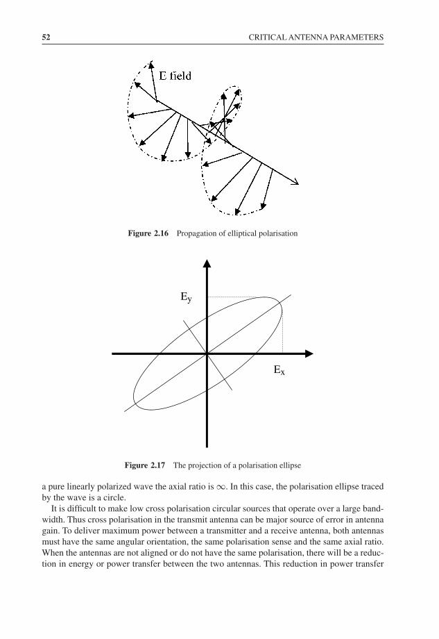
52 CRITICAL ANTENNA PARAMETERS
Figure 2.16 Propagation of elliptical polarisation
Ex
Ey
Figure 2.17 The projection of a polarisation ellipse
a pure linearly polarized wave the axial ratio is ∞. In this case, the polarisation ellipse tracedby the wave is a circle.
It is difficult to make low cross polarisation circular sources that operate over a large band-width. Thus cross polarisation in the transmit antenna can be major source of error in antennagain. To deliver maximum power between a transmitter and a receive antenna, both antennasmust have the same angular orientation, the same polarisation sense and the same axial ratio.When the antennas are not aligned or do not have the same polarisation, there will be a reduc-tion in energy or power transfer between the two antennas. This reduction in power transfer
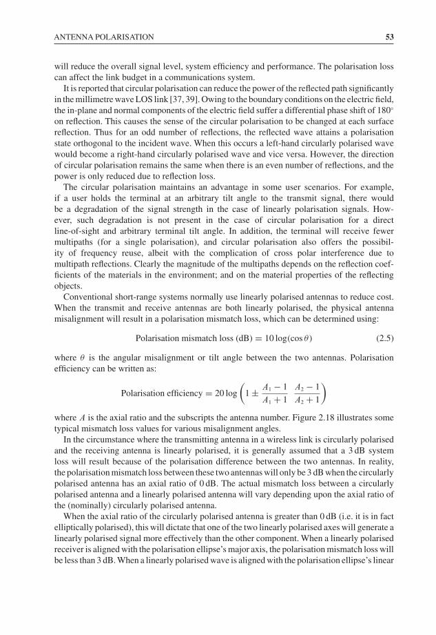
ANTENNA POLARISATION 53
will reduce the overall signal level, system efficiency and performance. The polarisation losscan affect the link budget in a communications system.
It is reported that circular polarisation can reduce the power of the reflected path significantlyin the millimetre wave LOS link [37, 39]. Owing to the boundary conditions on the electric field,the in-plane and normal components of the electric field suffer a differential phase shift of 180◦
on reflection. This causes the sense of the circular polarisation to be changed at each surfacereflection. Thus for an odd number of reflections, the reflected wave attains a polarisationstate orthogonal to the incident wave. When this occurs a left-hand circularly polarised wavewould become a right-hand circularly polarised wave and vice versa. However, the directionof circular polarisation remains the same when there is an even number of reflections, and thepower is only reduced due to reflection loss.
The circular polarisation maintains an advantage in some user scenarios. For example,if a user holds the terminal at an arbitrary tilt angle to the transmit signal, there wouldbe a degradation of the signal strength in the case of linearly polarisation signals. How-ever, such degradation is not present in the case of circular polarisation for a directline-of-sight and arbitrary terminal tilt angle. In addition, the terminal will receive fewermultipaths (for a single polarisation), and circular polarisation also offers the possibil-ity of frequency reuse, albeit with the complication of cross polar interference due tomultipath reflections. Clearly the magnitude of the multipaths depends on the reflection coef-ficients of the materials in the environment; and on the material properties of the reflectingobjects.
Conventional short-range systems normally use linearly polarised antennas to reduce cost.When the transmit and receive antennas are both linearly polarised, the physical antennamisalignment will result in a polarisation mismatch loss, which can be determined using:
Polarisation mismatch loss (dB) = 10 log(cos θ) (2.5)
where θ is the angular misalignment or tilt angle between the two antennas. Polarisationefficiency can be written as:
Polarisation efficiency = 20 log
(1 ± A1 − 1
A1 + 1
A2 − 1
A2 + 1
)
where A is the axial ratio and the subscripts the antenna number. Figure 2.18 illustrates sometypical mismatch loss values for various misalignment angles.
In the circumstance where the transmitting antenna in a wireless link is circularly polarisedand the receiving antenna is linearly polarised, it is generally assumed that a 3 dB systemloss will result because of the polarisation difference between the two antennas. In reality,the polarisation mismatch loss between these two antennas will only be 3 dB when the circularlypolarised antenna has an axial ratio of 0 dB. The actual mismatch loss between a circularlypolarised antenna and a linearly polarised antenna will vary depending upon the axial ratio ofthe (nominally) circularly polarised antenna.
When the axial ratio of the circularly polarised antenna is greater than 0 dB (i.e. it is in factelliptically polarised), this will dictate that one of the two linearly polarised axes will generate alinearly polarised signal more effectively than the other component. When a linearly polarisedreceiver is aligned with the polarisation ellipse’s major axis, the polarisation mismatch loss willbe less than 3 dB. When a linearly polarised wave is aligned with the polarisation ellipse’s linear
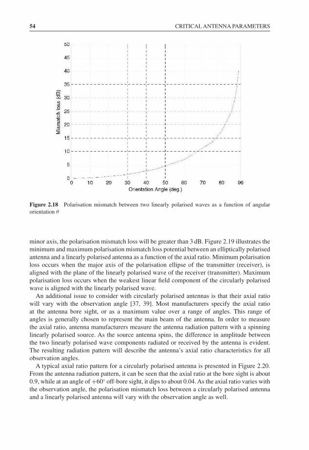
54 CRITICAL ANTENNA PARAMETERS
Figure 2.18 Polarisation mismatch between two linearly polarised waves as a function of angularorientation θ
minor axis, the polarisation mismatch loss will be greater than 3 dB. Figure 2.19 illustrates theminimum and maximum polarisation mismatch loss potential between an elliptically polarisedantenna and a linearly polarised antenna as a function of the axial ratio. Minimum polarisationloss occurs when the major axis of the polarisation ellipse of the transmitter (receiver), isaligned with the plane of the linearly polarised wave of the receiver (transmitter). Maximumpolarisation loss occurs when the weakest linear field component of the circularly polarisedwave is aligned with the linearly polarised wave.
An additional issue to consider with circularly polarised antennas is that their axial ratiowill vary with the observation angle [37, 39]. Most manufacturers specify the axial ratioat the antenna bore sight, or as a maximum value over a range of angles. This range ofangles is generally chosen to represent the main beam of the antenna. In order to measurethe axial ratio, antenna manufacturers measure the antenna radiation pattern with a spinninglinearly polarised source. As the source antenna spins, the difference in amplitude betweenthe two linearly polarised wave components radiated or received by the antenna is evident.The resulting radiation pattern will describe the antenna’s axial ratio characteristics for allobservation angles.
A typical axial ratio pattern for a circularly polarised antenna is presented in Figure 2.20.From the antenna radiation pattern, it can be seen that the axial ratio at the bore sight is about0.9, while at an angle of +60◦ off-bore sight, it dips to about 0.04. As the axial ratio varies withthe observation angle, the polarisation mismatch loss between a circularly polarised antennaand a linearly polarised antenna will vary with the observation angle as well.
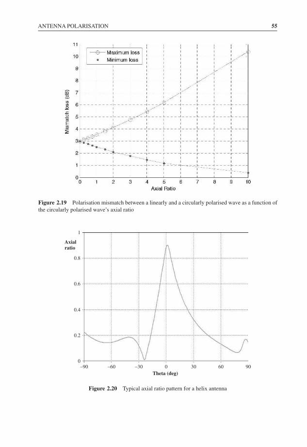
ANTENNA POLARISATION 55
Figure 2.19 Polarisation mismatch between a linearly and a circularly polarised wave as a function ofthe circularly polarised wave’s axial ratio
–900
0.2
0.4
0.6
0.8
1
–60 –30 0 30 60 90Theta (deg)
Axialratio
Figure 2.20 Typical axial ratio pattern for a helix antenna
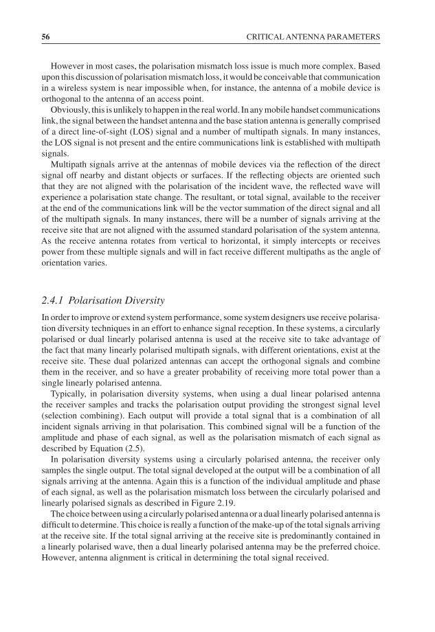
56 CRITICAL ANTENNA PARAMETERS
However in most cases, the polarisation mismatch loss issue is much more complex. Basedupon this discussion of polarisation mismatch loss, it would be conceivable that communicationin a wireless system is near impossible when, for instance, the antenna of a mobile device isorthogonal to the antenna of an access point.
Obviously, this is unlikely to happen in the real world. In any mobile handset communicationslink, the signal between the handset antenna and the base station antenna is generally comprisedof a direct line-of-sight (LOS) signal and a number of multipath signals. In many instances,the LOS signal is not present and the entire communications link is established with multipathsignals.
Multipath signals arrive at the antennas of mobile devices via the reflection of the directsignal off nearby and distant objects or surfaces. If the reflecting objects are oriented suchthat they are not aligned with the polarisation of the incident wave, the reflected wave willexperience a polarisation state change. The resultant, or total signal, available to the receiverat the end of the communications link will be the vector summation of the direct signal and allof the multipath signals. In many instances, there will be a number of signals arriving at thereceive site that are not aligned with the assumed standard polarisation of the system antenna.As the receive antenna rotates from vertical to horizontal, it simply intercepts or receivespower from these multiple signals and will in fact receive different multipaths as the angle oforientation varies.
2.4.1 Polarisation Diversity
In order to improve or extend system performance, some system designers use receive polarisa-tion diversity techniques in an effort to enhance signal reception. In these systems, a circularlypolarised or dual linearly polarised antenna is used at the receive site to take advantage ofthe fact that many linearly polarised multipath signals, with different orientations, exist at thereceive site. These dual polarized antennas can accept the orthogonal signals and combinethem in the receiver, and so have a greater probability of receiving more total power than asingle linearly polarised antenna.
Typically, in polarisation diversity systems, when using a dual linear polarised antennathe receiver samples and tracks the polarisation output providing the strongest signal level(selection combining). Each output will provide a total signal that is a combination of allincident signals arriving in that polarisation. This combined signal will be a function of theamplitude and phase of each signal, as well as the polarisation mismatch of each signal asdescribed by Equation (2.5).
In polarisation diversity systems using a circularly polarised antenna, the receiver onlysamples the single output. The total signal developed at the output will be a combination of allsignals arriving at the antenna. Again this is a function of the individual amplitude and phaseof each signal, as well as the polarisation mismatch loss between the circularly polarised andlinearly polarised signals as described in Figure 2.19.
The choice between using a circularly polarised antenna or a dual linearly polarised antenna isdifficult to determine. This choice is really a function of the make-up of the total signals arrivingat the receive site. If the total signal arriving at the receive site is predominantly contained ina linearly polarised wave, then a dual linearly polarised antenna may be the preferred choice.However, antenna alignment is critical in determining the total signal received.
ANTENNA POLARISATION 57
With a dual polarised antenna, the signal loss due to a polarisation mismatch will be between0 and 3 dB. If a circularly polarised antenna is used (assuming a 1 dB maximum axial ratioover the main beam), the signal loss due to a polarisation mismatch will be between 2.5 and3.5 dB. If the total signal arriving at the antenna is comprised of a random sample of multiplelinearly polarised signals, the circularly polarised antenna will be able to detect the waves, andmay be the correct choice for a receiver in a dense scattering environment. With a dual linearlypolarised antenna the polarisation mismatch loss will generally be greater than 3 dB.
A number of researchers have shown that dual polarisation diversity, using vertical andhorizontal polarisations, can improve the received signal-to-noise ratio [40, 41]. In addition,the performance of a three-branch orthogonal polarisation diversity system in a scatteringenvironment has been investigated and compared to that of a dual-channel polarisation diversitysystem. The results show that the former system has a 2 dB advantage over the latter [42].The results also suggest that the use of horizontal polarisation at the transmitter results in a2 dB improvement over a vertically polarised transmitter. This observation could be explainedby the fact that in the indoor environment (where the receive antennas were located), themajority of reflectors are horizontal (floors and ceilings). The work presented showed thatthere are clear benefits to using a three-branch polarisation diversity scheme to improve the linkbudget.
Diversity schemes have been shown to be highly efficient in mitigating the effects of mul-tipath fading. The three-branch polarisation diversity schemes [39, 40] can also be applied tomillimetre wave antenna systems. This particular scheme uses three orthogonal antennas atthe receiver to increase the link budget by more than 6 dB and 2 dB for the Rayleigh and dual-channel cases, respectively. The approach has an added advantage of being relatively smalland compact, since the antenna elements can be co-located, making it suitable for applicationswhere space is limited. This ability of the system to provide three uncorrelated copies of thetransmitted signal also implies that it can potentially be deployed at both the transmitter andreceiver in a conventional multiple-input multiple-output (MIMO) arrangement, to enhanceboth the capacity and the link budget of the channel. However, in this section emphase willbe placed on the operation of the scheme as a diversity system (for a robust channel), while theMIMO analysis will be reported in a future publication. The performance of the triple polarscheme was analysed for the indoor environment in Reference [42]. It was envisaged that usersrequiring high-speed data services will typically be located in this environment and will berelatively stationary, with data terminals larger than current mobile phones which are capableof accommodating the diversity antennas [43]. The polarisation diversity scheme can thenbe implemented at the access points and/or at the mobile devices to enhance the link budget.
The three-branch polarisation diversity system employs three orthogonal antennas whichmay be implemented as either electric or magnetic elements (a total energy antenna can be con-structed by using both electric and magnetic elements). In this configuration, three orthogonalelectric field detectors were used. One of the antennas is in a vertical position and two are inorthogonal horizontal positions (H1 and H2), as shown in Figure 2.21. As mentioned above,one of the major benefits of this configuration is that the antennas are co-located and can bedesigned to occupy minimal space. This is particularly important in access points where spaceis limited, and also in handsets where the device size cannot accommodate spatially separatedantennas. One of the problems of having closely separated antennas is the mutual couplingbetween the elements, which can adversely affect the application of the array in a diversitysystem (the communications channels then become correlated). However, by careful design,
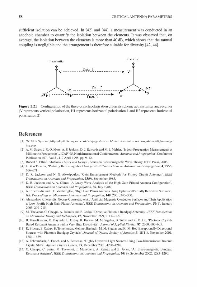
58 CRITICAL ANTENNA PARAMETERS
sufficient isolation can be achieved. In [42] and [44], a measurement was conducted in ananechoic chamber to quantify the isolation between the elements. It was observed that, onaverage, the isolation between the elements is more than 40 dB, which shows that the mutualcoupling is negligible and the arrangement is therefore suitable for diversity [42, 44].
Figure 2.21 Configuration of the three-branch polarisation diversity scheme at transmitter and receiver(V represents vertical polarisation, H1 represents horizontal polarisation 1 and H2 represents horizontalpolarisation 2)
References[1] ‘60 GHz System’, http://dept106.eng.ox.ac.uk/wb/pages/research/microwave/uture-radio-systems/60ghz-imag-
ing.php[2] A. M. Street, J. G. O. Moss, A. P. Jenkins, D. J. Edwards and M. J. Mehler, ‘Indoor Propagation Measurements at
Millimetric Frequencies’„ ICAP’95, Ninth International Conference on ‘Antennas and Propagation’, ConferencePublication 407 , Vol.2 , 4–7 April 1995, pp. 9–12.
[3] Robert S. Elliott, ‘Antenna Theory and Design’, Series on Electromagnetic Wave Theory, IEEE Press, 2006.[4] G. Von Trentini, ‘Partially Reflecting Sheet Arrays’ IEEE Transactions on Antennas and Propagation, 4, 1956,
666–671.[5] D. R. Jackson and N. G. Alexópoulos, ‘Gain Enhancement Methods for Printed Circuit Antennas’, IEEE
Transactions on Antennas and Propagation, 33(9), September 1985.[6] D. R. Jackson and A. A. Oliner, ‘A Leaky-Wave Analysis of the High-Gain Printed Antenna Configuration’,
IEEE Transactions on Antennas and Propagation, 36, July 1988.[7] A. P. Feresidis and J. C. Vardaxoglou, ‘High Gain PlanarAntenna Using Optimised Partially Reflective Surfaces’,
IEE Proceedings on Microwave Antennas and Propagation, 148, 2001, 345–350.[8] Alexandros P. Feresidis, George Goussetis, et al., ‘Artificial Magnetic Conductor Surfaces and Their Application
to Low-Profile High-Gain Planar Antennas’, IEEE Transactions on Antennas and Propagation, 53(1), January2005, 209–215.
[9] M. Thévenot, C. Cheype, A. Reineix and B. Jecko, ‘Directive Photonic Bandgap Antennas’, IEEE Transactionson Microwave Theory and Techniques, 47, November 1999, 2115–2122.
[10] B. Temelkuaran, M. Bayindir, E. Ozbay, R. Biswas, M. M. Sigalas, G. Tuttle and K. M. Ho, ‘Photonic Crystal-Based Resonant Antenna with a Very High Directivity’, Journal of Applied Physics, 87, 2000, 603–605.
[11] R. Biswas, E. Ozbay, B. Temelkuran, Mehmet Bayindir, M. M. Sigalas and K.-M. Ho, ‘Exceptionally DirectionalSources with Photonic-Bandgap Crystals’, Journal of Optical Society of America B, 18(11), November 2001,1684–1689.
[12] A. Fehrembach, S. Enoch, and A. Sentenac, ‘Highly Directive Light Sources Using Two-Dimensional PhotonicCrystal Slabs’, Applied Physics Letters, 79, December 2001, 4280–4282.
[13] C. Cheype, C. Serier, M. Thevenot, T. Monediere, A. Reinex and B. Jecko, ‘An Electromagnetic BandgapResonator Antenna’, IEEE Transactions on Antennas and Propagation, 50( 9), September 2002, 1285–1290.

REFERENCES 59
[14] Y. J. Lee, J. Yeo, R. Mittra and W. S. Park, ‘Application of Electromagnetic Bandgap (EBG) Superstrates withControllable Defects for a Class of Patch Antennas as Spatial Angular Filters’, IEEE Transactions on Antennasand Propagation, 53(1), January 2005, 224–235.
[15] R. Gardelli, M. Albani and F. Capolino, ‘Array Thinning by Using Antennas in a Fabry–Perot Cavity for GainEnhancement’, IEEE Transactions on Antennas and Propagation, 54(7), July 2006.
[16] A. R. Weily, L. Horvath, K. P. Esselle, B. C. Sanders and T. S. Bird, ‘A Planar Resonator Antenna Based on aWoodpile EBG Material’, IEEE Transactions on Antennas and Propagation, 53(1), January 2005, 216–223.
[17] K. C. Gupta, ‘Narrow Beam Antenna Using an Artificial Dielectric Medium with Permittivity Less Than Unity’,Electronic Letters, 7(1), January 1971,16.
[18] I. J. Bahl and K. C. Gupta, ‘A Leaky-Wave Antenna Using an Artificial Dielectric Medium, IEEE Transactionson Antennas and Propagation, AP-22, January 1974, 119–122.
[19] S. Enoch, G. Tayeb, P. Sabouroux, N. Guérin and P. Vincent, ‘A Metamaterial for Directive Emission,’ PhysicalReview Letters, 89, November 2002, 213902-1–213902-4.
[20] G. Lovat, P. Burghignoli, F. Capolino, D. R. Jackson and D. R. Wilton, ‘Analysis of Directive Radiation from aLine Source in a Metamaterial Slab with Low Permittivity’, IEEE Transactions on Antennas and Propagation,54(3), March 2006, 1017–1030.
[21] G. Lovat, P. Burghignoli, F. Capolino, et al., ‘High Directivity in Low-Permittivity Metamaterial Slabs: Ray-Opticvs Leaky-Wave Models’, Microwave and Optical Technology Letters, 48(12), December 2006, 2542–2548.
[22] G. Lovat, P. Burghignoli, F. Capolino and D. R. Jackson, ‘On the Combinations of Low/High Permittivity and/orPermeability Substrates or Highly Directive Planar Metamaterial Antennas’, IEE Proceedings on MicrowaveAntennas and Propagation, Special Issue on Metamaterials, Vol. 1, February 2007.
[23] G. Lovat, P. Burghignoli, F. Capolino and D. R. Jackson, ‘Highly-Directive Planar Leaky-Wave Antennas:A Comparison between Metamaterial-Based and Conventional Designs’, EuMA (European MicrowaveAssociation) Proceedings, Vol. 2, 2006.
[24] K. Huang and Z. Wang ‘V-Band Patch-Fed Rod Antennas for High Data-Rate Wireless Communications’, IEEETransactions on Antennas and Propagation, 54(1), January 2006, 297–300.
[25] W. Menzel, D. Pilz and M. Al-Tikriti, ‘Millimeter-Wave Folded Reflector Antennas with High Gain, Low Loss,and Low Profile’, IEEE Antennas and Propagation Magazine, 44(3), June 2002, 24–29.
[26] F. Colomb, K. Hur, W. Stacey and M. Grigas, ‘Annular Slot Antennas on Extended Hemispherical Dielec-tric Lenses’, Antennas and Propagation Society International Symposium, 1996, AP-S Digest, 3, July 1996,2192–2195.
[27] S. Sierra-Garcia and J.-J. Laurin, ‘Study of a CPW Inductively Coupled Slot Antenna’, IEEE Transactions onAntennas and Propagation, 47(1), January 1999, 58–64.
[28] W. Y. Ali-Ahmad, G. V. Eleftheriades, L. P. B. Katehi and G. M. Rebeiz, ‘Millimeter-Wave Integrated-Horn Antenna. II. Experiment’, IEEE Transactions on Antennas and Propagation, 39(11), November 1991,1582–1586.
[29] J. A. Besley, N. N. Akhmediev and P. D. Miller, Optics Letters, 22(15), 1 August 1997.[30] X. Wu, G. V. Eleftheriades and T. E. van Deventer-Perkins, ‘Design and Characterization of Single- and
Multiple-Beam mm-Wave Circularly Polarized Substrate Lens Antennas for Wireless Communications’, IEEETransactions on Microwave Theory and Techniques, 49(3), March 2001, 431–441.
[31] M. Sironen, Y. Qian and T. Itoh, ‘A60 GHz Conical HornAntenna Excited with Quasi-YagiAntenna’, MicrowaveSymposium Digest, IEEE MTT-S International, 1, 2001, 547–550.
[32] Xidong Wu and G. V. Eleftheriades, ‘Two-Lens and Lens-Fed Reflector Antenna Systems for mm-WaveWireless Communications’, IEEE Antennas and Propagation Society International Symposium, 2000, Vol. 2,pp. 660–663.
[33] L. J. Chu, ‘Physical Limitations of Omni-directional Antennas’, Journal of Applied Physics, 19, December 1948,1163–1175.
[34] R. F. Harrington, ‘On the Gain and Beamwidth of Directional Antennas’, IRE Transactions on Antennas andPropagation, 6, 1958, 219–225.
[35] W. Geyi, ‘Physical Limitations of Antenna’, IEEE Transactions on Antennas and Propagation, 51(8), August2003, 2116–2123.
[36] R. F. Harrington, ‘Effect of Antenna Size on Gain, Bandwidth, and Efficiency’, Journal of Research NationalBureau of Standards – D. Radio Propagation, 64D(1), January/February 1960.
[37] A. C. Ludwig, ‘The Definition of Cross Polarization, IEEE Transactions on Antennas and Propagation,AP-21(1),January 1973, 116–119.

60 CRITICAL ANTENNA PARAMETERS
[38] R. L. Fante, ‘Quality Factor of General Ideal Antennas’, IEEE Transactions on Antennas and Propagation,AP-17(2), March 1969, 151–155.
[39] T. Manabe et al., ‘Polarization Dependence of Multipath Propagation and High-Speed Transmission Character-istics of Indoor Millimeter-Wave Channel at 60GHz’, IEEE Transactions on Vehicular Technology, 44(2), May1995.
[40] L. Lukama, K. Konstantinou and D.J. Edwards, ‘Polarization Diversity Performance for UMTS’, Proceedingsof the International Conference on ‘Antennas and Propagation’ (ICAPZOOI), April 2001, Manchester,England.
[41] R.G. Vaughan, ‘Polarization Diversity in Mobile Communications’, IEEE Transactions on Vehicular Technology,39(3), August 1990, 177–186.
[42] L. C. Lukama, D. J. Edwards and A. Wain, ‘Application of Three-Branch Polarisation Diversity in the IndoorEnvironment’, IEE Proceedings on Communications, 150(5), October 2003, 399–403.
[43] L.C. Lukama, K. Konstantinou and D.J. Edwards, ‘Performance of a Three-Branch Orthogonal PolarizationDiversity Scheme’, IEEE Vehicular Technology Conference Proceedings, Fall, 2001, 2033–2037.
[44] L. Lukama, K. Konstantinou and D.J. Edwards, ‘Three-Branch Orthogonal Polarization Diversity Scheme’,Electronic Letters, 37(20), 2001, 1258–1259.
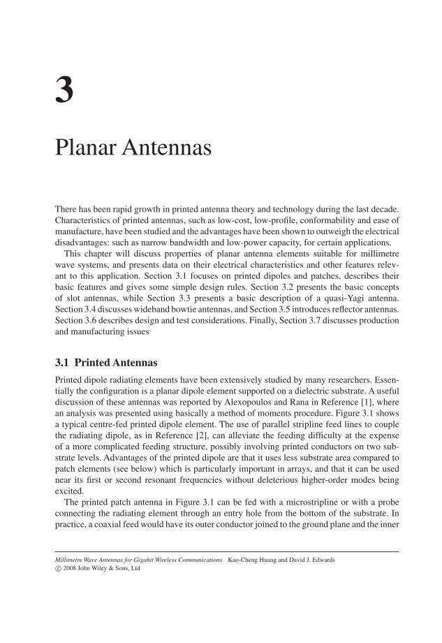
3Planar Antennas
There has been rapid growth in printed antenna theory and technology during the last decade.Characteristics of printed antennas, such as low-cost, low-profile, conformability and ease ofmanufacture, have been studied and the advantages have been shown to outweigh the electricaldisadvantages: such as narrow bandwidth and low-power capacity, for certain applications.
This chapter will discuss properties of planar antenna elements suitable for millimetrewave systems, and presents data on their electrical characteristics and other features relev-ant to this application. Section 3.1 focuses on printed dipoles and patches, describes theirbasic features and gives some simple design rules. Section 3.2 presents the basic conceptsof slot antennas, while Section 3.3 presents a basic description of a quasi-Yagi antenna.Section 3.4 discusses wideband bowtie antennas, and Section 3.5 introduces reflector antennas.Section 3.6 describes design and test considerations. Finally, Section 3.7 discusses productionand manufacturing issues
3.1 Printed Antennas
Printed dipole radiating elements have been extensively studied by many researchers. Essen-tially the configuration is a planar dipole element supported on a dielectric substrate. A usefuldiscussion of these antennas was reported by Alexopoulos and Rana in Reference [1], wherean analysis was presented using basically a method of moments procedure. Figure 3.1 showsa typical centre-fed printed dipole element. The use of parallel stripline feed lines to couplethe radiating dipole, as in Reference [2], can alleviate the feeding difficulty at the expenseof a more complicated feeding structure, possibly involving printed conductors on two sub-strate levels. Advantages of the printed dipole are that it uses less substrate area compared topatch elements (see below) which is particularly important in arrays, and that it can be usednear its first or second resonant frequencies without deleterious higher-order modes beingexcited.
The printed patch antenna in Figure 3.1 can be fed with a microstripline or with a probeconnecting the radiating element through an entry hole from the bottom of the substrate. Inpractice, a coaxial feed would have its outer conductor joined to the ground plane and the inner
Millimetre Wave Antennas for Gigabit Wireless Communications Kao-Cheng Huang and David J. Edwardsc© 2008 John Wiley & Sons, Ltd
62 PLANAR ANTENNAS
00
0.1
0.2
0.3
0.4
0.5
0.1 0.2 0.3 0.4
d / l0
L /l
0
Patch
Dipole
PRINTED DIPOLE MICROSTRIP PATCH
L
dd
W
L
1 surface wave 2 surface wave
Figure 3.1 Resonant lengths of a printed dipole and a microstrip patch versus d for polystyrene sub-strate. Patch width W = 0.3 λ0.At the top are shown the printed dipole and patch geometries. (Reproducedby permission of © 1983 IEEE [3])
conductor, or the feeder, would pass through the dielectric substrate and connect to the radiatingelement. It is observed that the rectangular patch needs more substrate area than the dipoleand that a probe-type feed may be difficult to fabricate on monolithic substrates, such asalumina or quartz substrates. A feeding issue exists with microstripline feeds, since for amicrostripline, the line width determines its characteristic impedance (for a given substrate)and is relatively constant with frequency. The size of a resonant patch antenna, however,decreases with increasing frequency, so that a given microstrip feed line on a substrate hasan effective upper frequency limit beyond which the resonant patch width would be narrowerthan the feed line width.
It should be noted that there are intrinsic differences in the electrical operation of printeddipoles and patches. The first resonance of a printed dipole, like a half-wave dipole in free space,is a series-type resonance as the current is driven in the same direction as the driving electricfield. On the other hand, the first resonance of a patch antenna is a parallel-type (anti)resonanceas the current is in the plane of the patch but the field is between the conducting plates of thestructure. This difference is a result of the field structure created in the vicinity of the elementby a particular feed.
For a dipole, the feed couples to the electric field component along the dipole axis, whilea coaxial or microstripline-fed patch antenna is coupled by the electric field component

PRINTED ANTENNAS 63
perpendicular to the substrate. Printed dipoles and patches, however, have similar currentdistributions; thus the radiation patterns are similar [1, 4].
For a nearly square patch with dimensions a and b, the design procedure can be listed asfollows:
(i) Find the resonant frequency from the effective patch dimensions a and b, satisfying:
a ≥ c
2f√
εr
≥ b
where c is the speed of light and εr is the relative dielectric constant of the material. Thetrue physical dimensions for W and L are smaller than a and b because of the fringingeffect.
(ii) Choose the operation frequency and bandwidth.(iii) Choose the appropriate substrate.(iv) Estimate the power loss.(v) Estimate the resonant resistance and quality factor.
(vi) Determine the feeding method.(vii) Occasionally, iterations are needed for fine-tuning the antenna performance.
These points are discussed step by step as follows.
(i) Resonant FrequencyThe first consideration in the design of a printed antenna element is the length L of the elementrequired for resonance. This length is a function of substrate thickness d and the relativedielectric constant εr , and, in the case of a microstrip patch, a function of the patch widthW . Because the dielectric material only exists in the region of space underneath the antennaelement and not in the space above, the resonant length does not scale with the dielectricconstant as 1/
√εr (which is only used by an antenna in a homogeneous medium).
Figure 3.1 shows the required lengths for the first resonance of a printed dipole and a rect-angular microstrip patch element versus substrate thickness d, for a Teflon TM material. Thepatch width is W = 0.3 λ0 (λ0 is the free space wavelength). The dipole length varies lessthan 6 % for 0 < d < 0.5b, and is slightly longer than the patch length, which varies propor-tionately more with d . An interesting feature of the patch antenna is that it stops resonatingfor substrate thicknesses greater than 0.11 λ0. With increasing substrate thickness, the trend istowards an entirely inductive input impedance locus (due to the phase relationship between cur-rent and applied field/voltage). This effect occurs for both probe-type and microstripline-typefeeds.
This situation is probably undesirable in most cases, and so the use of patches on thicksubstrates may not be practical unless some way of countering this inductive trend is used, forexample by using a capacitive-gap coupling from a feed line. The dotted continuation of thepatch length curve in Figure 3.1 is given only to show the length chosen for the calculation ofother data presented later in Figure 3.2. An increase in patch width W can reduce the resonantlength by a few per cent; the length reduction is greater for thicker substrates.
64 PLANAR ANTENNAS
(ii) Frequency BandwidthFrequency bandwidth is one of the important antenna parameters. It is defined as the half-power width of the equivalent circuit impedance response. For a series-type resonance [2], thisbandwidth (BW) is:
BW = 2R
ω0 dX/dω|ω0
(3.1)
where the input impedance at the resonant frequency ω0, Z, is equal to R + jX. For a parallel-type resonance, Equation (3.1) is used with R replaced by the conductance G, and X replacedby the inverse of the reactance B; here the input admittance Y at resonance is equal to G+ jB.The derivative in Equation (3.1) can be evaluated by calculating the input impedance at twofrequencies near resonance and using a finite difference approximation.
As discussed by Harrington [5], the lowest achievable Q of an antenna is inversely relatedto the antenna volume (since Q depends on the ratio of the stored energy [depends on L3, thevolume] and to the dissipated energy [linear in L or L2, the length or area]). Since the patchantenna encompasses a greater volume than the printed dipole, its Q can be lower than the Q
of the dipole, and hence the operational bandwidth can be greater.
(iii) Substrate CharacteristicsTo produce printed antennas, it is necessary to select a material that is mechanically andelectromagnetically stable. This choice of substrate is based on the fact that the permittivityrange is from 1.2 to 13 and that these materials are either in use today or are expected to bein use for millimetre wave antenna systems in the future. Because of space considerations,not all materials available today will be compared here, but it is felt that these examples arerepresentative and other common substrate materials have properties roughly in the range ofthose considered here.
Teflon and related products like Rexolite™ and RT/Duroid 5870/5880™ have been usedextensively in the microwave band [6]. Quartz substrates have very good dimensional stabilityand are often used in microwave integrated circuits. Gallium arsenide is one of the low-losssubstrate materials used for monolithic microwave integrated circuits. DuPont™ 943 Low LossGreen Tape™ [7] can be used with gold, silver and mixed-metal material systems, and can beconsidered for use by millimetre wave circuit designers and manufacturers.
The dielectric loss factor, also known as the dissipation factor, is defined as the tangentof the loss angle (tan δ, or the loss tangent). The loss factor represents the ratio of resist-ance to reactance of a parallel equivalent circuit of the ceramic element. Alternatively, for aprimarily reactive circuit model, the degree to which the angle differs from 90◦ would be acase of a lossless device. Thus the real and imaginary components of the dielectric constantare quantified. The dielectric constant (ε) and loss factor (tan δ) can be measured using astandard impedance bridge or an impedance analyser. Some typical examples are identified inTable 3.1.
(iv) Power LossPower loss can be caused by surface waves, the dielectric material, and implementationtolerances, etc. Here the first two losses will be discussed:

PRINTED ANTENNAS 65
Table 3.1 Electrical properties of microwave substrates [8]
0.0001 0.0002 0.0003 0.0004 0.0005 0.0006 0.0007 0.0008 0.0009 0.001 0.002 0.005 0.010 0.050 0.100Loss tangent
perm
ittiv
ity
MgCO3
1.0
1.2
2
2.1
2.2
2.3
2.4
2.5
3
4
5
6
7
8
9
10
12.5
Teflon
Polypropylene
Polyethylene
Polystyrene
Quarz
BN
Mica
BeO
GaAs
Al2O3MgOSapphire
GreenTape943
MgTiO3
• Power loss due to surface waves
Both TE and TM surface waves can be excited on a grounded dielectric substrate. The cut-offfrequency of these modes is given by [5]:
fc = nc
4d√
εr − 1(3.2)
where c is the speed of light and n = 0, 1, 2, 3 for the TM0, TE1, TM2, TE3 surface modes,respectively. Note that the TM0 mode has a zero cut-off frequency, so that it can be generatedfor any substrate thickness. As the substrate becomes electrically thicker, more surface modescan exist and the coupling to the lower-order modes can become stronger. For thin substrates(d <0.01 λ0) this surface wave excitation is generally regarded as unimportant.
For thicker substrates these surface waves may have a detrimental effect on printed antennaperformance. Surface wave power launched in an infinitely wide substrate, would not contributeto the main beam radiation and so can be considered as a loss mechanism. In this case, theradiation efficiency can then be defined as:
e = Prad
Prad + Psw
(3.3)
66 PLANAR ANTENNAS
where Prad is the power radiated via the space wave (the main beam power), and Psw is the powercoupled into surface waves. Prad + Psw is then the total power delivered to the printed antennaelement. Here dielectric losses have been ignored. The effect of a finite-sized substrate is to dif-fract the surface wave energy from the substrate edges, possibly causing undesirable effects onsidelobe level, polarisation or main beam shape. In general, for low sidelobe performance, theedge excitation needs to be low and the aperture excitation needs to vary slowly over the patch.Low sidelobe requirements tend to conflict with high aperture efficiency. However, by a carefulbalancing of the modal excitation, a good compromise between mainlobe gain and sidelobesuppression can be achieved. A high current excitation over as much of the patch as possible(efficiency) is aimed for, but with the current tapering smoothly to zero at the edges. Surfacewaves could also be diffracted by or coupled to feed lines or components on the substrate.
In the moment method formulation, surface wave fields and space wave fields are easilyseparated from the Sommerfeld-type integral expression for the total fields of an elementalcurrent source on a grounded dielectric slab. The surface waves arise from the residues of thecontour integral. Since in the moment method the impedance matrix elements are expressed interms of integrals of the fields from the modal expansion, these elements can be separated, as:
Zmn = Zradmn
+ Zswmn
(3.4)
where Zmn represents the matrix element using the total field, and Zradmn
and Zswmn
represent thedirect radiation (the space wave) and the surface wave contributions, respectively. Then, if In
represents the current on the nth expansion mode, the total input power can be written as:
Ptot = Re∑
n
∑m
I ∗nZmnIm (3.5)
and the radiated power can be written as:
Prad = Re∑
n
∑m
I ∗nZrad
mnIm (3.6)
• Losses due to the dielectric
Power loss due to dielectric heating can be calculated by using the loss tangent and com-plex permittivity for the particular substrate dielectric material. For the half-wave dipole (aseries-type resonance), for example, the radiation efficiency based on the dielectric loss canbe calculated as:
η = Rr
Rr + RI
(3.7)
where Rr is the radiation resistance at the input terminals and RI is the loss resistance. Rr andRI can be found from the two calculations of the input impedance, one with tan δ = 0 and onewith tan δ �= 0. The radiation resistance is R = Re(Zin), for tan δ = 0 and the loss resistance isfound from Rr + RI = Re(Zin) with tan δ �= 0. This is an accurate procedure for small losses.For full-wave dipoles or microstrip patches (anti-resonances), the efficiency is calculated usingthe conductance in Equation (3.7). Note that efficiency as defined by Equation (3.7) does notinclude the power loss due to surface waves (although it does in fact include heating loss fromsurface wave fields).
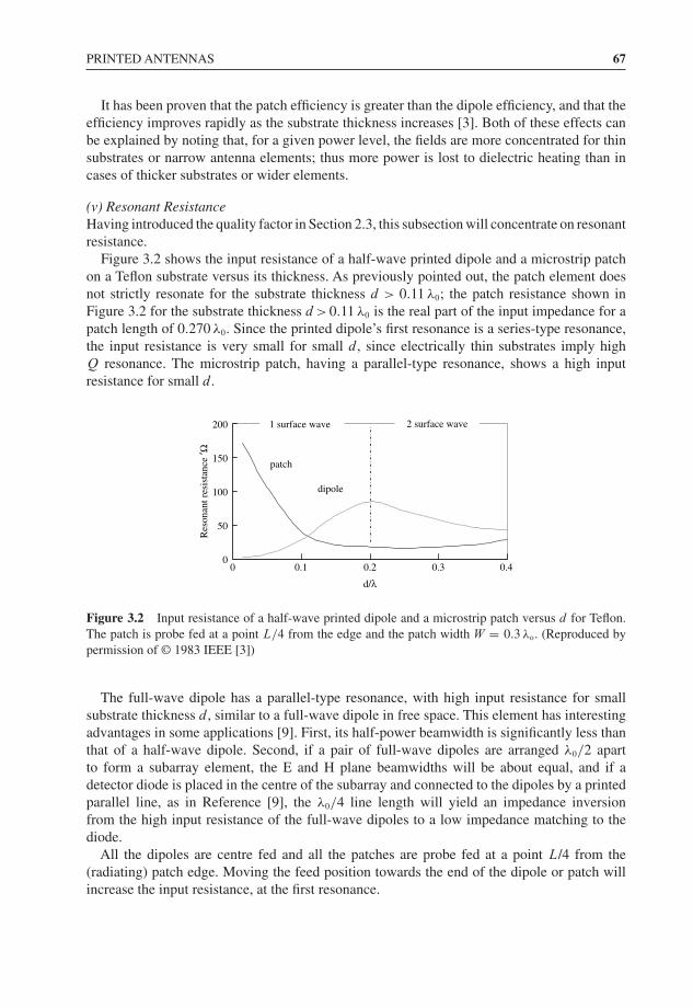
PRINTED ANTENNAS 67
It has been proven that the patch efficiency is greater than the dipole efficiency, and that theefficiency improves rapidly as the substrate thickness increases [3]. Both of these effects canbe explained by noting that, for a given power level, the fields are more concentrated for thinsubstrates or narrow antenna elements; thus more power is lost to dielectric heating than incases of thicker substrates or wider elements.
(v) Resonant ResistanceHaving introduced the quality factor in Section 2.3, this subsection will concentrate on resonantresistance.
Figure 3.2 shows the input resistance of a half-wave printed dipole and a microstrip patchon a Teflon substrate versus its thickness. As previously pointed out, the patch element doesnot strictly resonate for the substrate thickness d > 0.11 λ0; the patch resistance shown inFigure 3.2 for the substrate thickness d > 0.11 λ0 is the real part of the input impedance for apatch length of 0.270 λ0. Since the printed dipole’s first resonance is a series-type resonance,the input resistance is very small for small d , since electrically thin substrates imply highQ resonance. The microstrip patch, having a parallel-type resonance, shows a high inputresistance for small d .
patch
dipole
1 surface wave 2 surface wave200
150
100
50
00 0.1 0.2
d/λ
Res
onan
t res
ista
nce
′Ω
0.3 0.4
Figure 3.2 Input resistance of a half-wave printed dipole and a microstrip patch versus d for Teflon.The patch is probe fed at a point L/4 from the edge and the patch width W = 0.3 λo. (Reproduced bypermission of © 1983 IEEE [3])
The full-wave dipole has a parallel-type resonance, with high input resistance for smallsubstrate thickness d , similar to a full-wave dipole in free space. This element has interestingadvantages in some applications [9]. First, its half-power beamwidth is significantly less thanthat of a half-wave dipole. Second, if a pair of full-wave dipoles are arranged λ0/2 apartto form a subarray element, the E and H plane beamwidths will be about equal, and if adetector diode is placed in the centre of the subarray and connected to the dipoles by a printedparallel line, as in Reference [9], the λ0/4 line length will yield an impedance inversionfrom the high input resistance of the full-wave dipoles to a low impedance matching to thediode.
All the dipoles are centre fed and all the patches are probe fed at a point L/4 from the(radiating) patch edge. Moving the feed position towards the end of the dipole or patch willincrease the input resistance, at the first resonance.
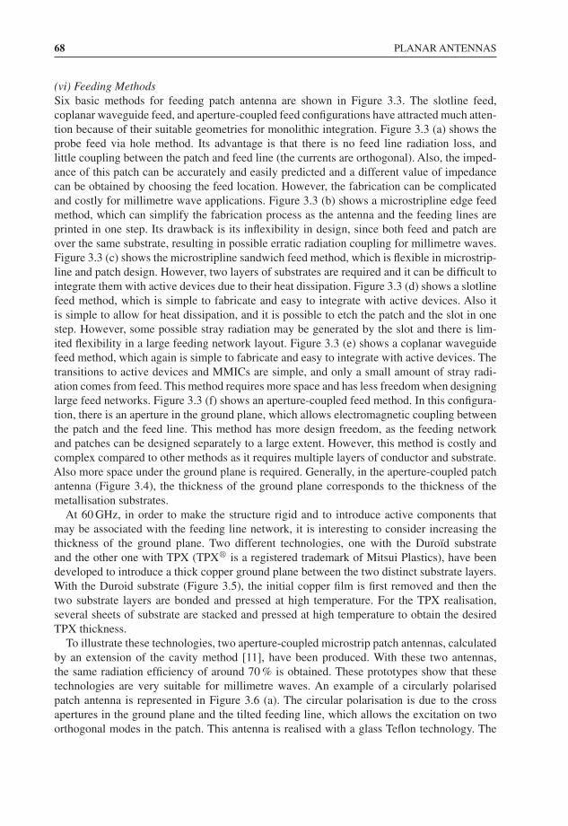
68 PLANAR ANTENNAS
(vi) Feeding MethodsSix basic methods for feeding patch antenna are shown in Figure 3.3. The slotline feed,coplanar waveguide feed, and aperture-coupled feed configurations have attracted much atten-tion because of their suitable geometries for monolithic integration. Figure 3.3 (a) shows theprobe feed via hole method. Its advantage is that there is no feed line radiation loss, andlittle coupling between the patch and feed line (the currents are orthogonal). Also, the imped-ance of this patch can be accurately and easily predicted and a different value of impedancecan be obtained by choosing the feed location. However, the fabrication can be complicatedand costly for millimetre wave applications. Figure 3.3 (b) shows a microstripline edge feedmethod, which can simplify the fabrication process as the antenna and the feeding lines areprinted in one step. Its drawback is its inflexibility in design, since both feed and patch areover the same substrate, resulting in possible erratic radiation coupling for millimetre waves.Figure 3.3 (c) shows the microstripline sandwich feed method, which is flexible in microstrip-line and patch design. However, two layers of substrates are required and it can be difficult tointegrate them with active devices due to their heat dissipation. Figure 3.3 (d) shows a slotlinefeed method, which is simple to fabricate and easy to integrate with active devices. Also itis simple to allow for heat dissipation, and it is possible to etch the patch and the slot in onestep. However, some possible stray radiation may be generated by the slot and there is lim-ited flexibility in a large feeding network layout. Figure 3.3 (e) shows a coplanar waveguidefeed method, which again is simple to fabricate and easy to integrate with active devices. Thetransitions to active devices and MMICs are simple, and only a small amount of stray radi-ation comes from feed. This method requires more space and has less freedom when designinglarge feed networks. Figure 3.3 (f) shows an aperture-coupled feed method. In this configura-tion, there is an aperture in the ground plane, which allows electromagnetic coupling betweenthe patch and the feed line. This method has more design freedom, as the feeding networkand patches can be designed separately to a large extent. However, this method is costly andcomplex compared to other methods as it requires multiple layers of conductor and substrate.Also more space under the ground plane is required. Generally, in the aperture-coupled patchantenna (Figure 3.4), the thickness of the ground plane corresponds to the thickness of themetallisation substrates.
At 60 GHz, in order to make the structure rigid and to introduce active components thatmay be associated with the feeding line network, it is interesting to consider increasing thethickness of the ground plane. Two different technologies, one with the Duroïd substrateand the other one with TPX (TPX� is a registered trademark of Mitsui Plastics), have beendeveloped to introduce a thick copper ground plane between the two distinct substrate layers.With the Duroid substrate (Figure 3.5), the initial copper film is first removed and then thetwo substrate layers are bonded and pressed at high temperature. For the TPX realisation,several sheets of substrate are stacked and pressed at high temperature to obtain the desiredTPX thickness.
To illustrate these technologies, two aperture-coupled microstrip patch antennas, calculatedby an extension of the cavity method [11], have been produced. With these two antennas,the same radiation efficiency of around 70 % is obtained. These prototypes show that thesetechnologies are very suitable for millimetre waves. An example of a circularly polarisedpatch antenna is represented in Figure 3.6 (a). The circular polarisation is due to the crossapertures in the ground plane and the tilted feeding line, which allows the excitation on twoorthogonal modes in the patch. This antenna is realised with a glass Teflon technology. The
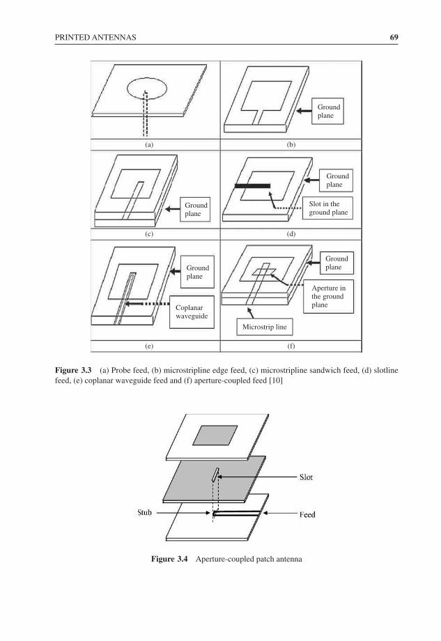
PRINTED ANTENNAS 69
(e) (f)
(c) (d)
(a) (b)
Groundplane
Groundplane
Groundplane
Groundplane
Groundplane
Slot in theground plane
Aperture inthe groundplaneCoplanar
waveguide
Microstrip line
Figure 3.3 (a) Probe feed, (b) microstripline edge feed, (c) microstripline sandwich feed, (d) slotlinefeed, (e) coplanar waveguide feed and (f) aperture-coupled feed [10]
Figure 3.4 Aperture-coupled patch antenna
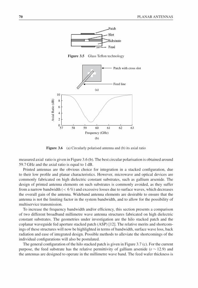
70 PLANAR ANTENNAS
Figure 3.5 Glass Teflon technology
(a)
(b)
0
2
4
6
8
10
57 58 59 60 61 62 63
Frequency (GHz)
Axi
al R
atio
(dB
)
Patch with cross slot
Feed line
Figure 3.6 (a) Circularly polarised antenna and (b) its axial ratio
measured axial ratio is given in Figure 3.6 (b). The best circular polarisation is obtained around59.7 GHz and the axial ratio is equal to 1 dB.
Printed antennas are the obvious choice for integration in a stacked configuration, dueto their low profile and planar characteristics. However, microwave and optical devices arecommonly fabricated on high dielectric constant substrates, such as gallium arsenide. Thedesign of printed antenna elements on such substrates is commonly avoided, as they sufferfrom a narrow bandwidth (< 6 %) and excessive losses due to surface waves, which decreasesthe overall gain of the antenna. Wideband antenna elements are desirable to ensure that theantenna is not the limiting factor in the system bandwidth, and to allow for the possibility ofmultiservice transmission.
To increase the frequency bandwidth and/or efficiency, this section presents a comparisonof two different broadband millimetre wave antenna structures fabricated on high dielectricconstant substrates. The geometries under investigation are the hilo stacked patch and thecoplanar waveguide fed aperture stacked patch (ASP) [12]. The relative merits and shortcom-ings of these structures will now be highlighted in terms of bandwidth, surface wave loss, backradiation and ease of integrated design. Possible methods to alleviate the shortcomings of theindividual configurations will also be postulated.
The general configuration of the hilo stacked patch is given in Figure 3.7 (c). For the currentpurpose, the feed substrate has the relative permittivity of gallium arsenide (ε ∼ 12.9) andthe antennas are designed to operate in the millimetre wave band. The feed wafer thickness is
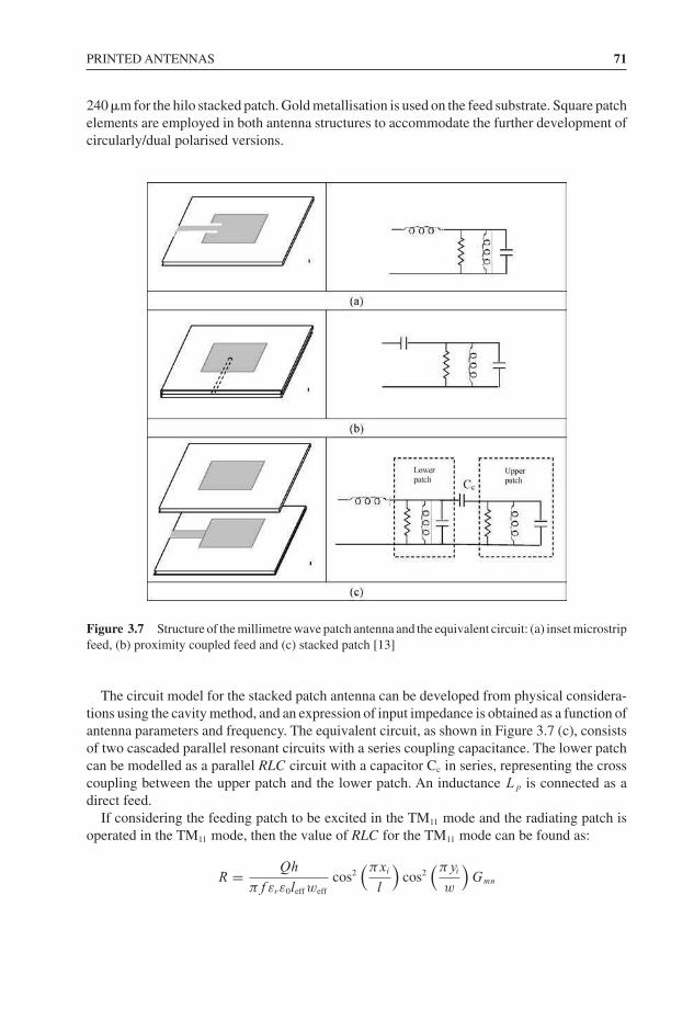
PRINTED ANTENNAS 71
240 �m for the hilo stacked patch. Gold metallisation is used on the feed substrate. Square patchelements are employed in both antenna structures to accommodate the further development ofcircularly/dual polarised versions.
Figure 3.7 Structure of the millimetre wave patch antenna and the equivalent circuit: (a) inset microstripfeed, (b) proximity coupled feed and (c) stacked patch [13]
The circuit model for the stacked patch antenna can be developed from physical considera-tions using the cavity method, and an expression of input impedance is obtained as a function ofantenna parameters and frequency. The equivalent circuit, as shown in Figure 3.7 (c), consistsof two cascaded parallel resonant circuits with a series coupling capacitance. The lower patchcan be modelled as a parallel RLC circuit with a capacitor Cc in series, representing the crosscoupling between the upper patch and the lower patch. An inductance Lp is connected as adirect feed.
If considering the feeding patch to be excited in the TM11 mode and the radiating patch isoperated in the TM11 mode, then the value of RLC for the TM11 mode can be found as:
R = Qh
πf εrε0leff weff
cos2(πxi
l
)cos2
(πyi
w
)Gmn
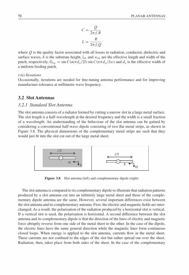
72 PLANAR ANTENNAS
C = Q
2πfrR
L = R
2πfrQ
where Q is the quality factor associated with all losses in radiation, conductor, dielectric andsurface waves, h is the substrate height, leff and weff are the effective length and width of thepatch, respectively, Gmn = sin C(mπdp/2l) sin C(nπdp/2w) and dp is the effective width ofa uniform feeding patch.
(vii) IterationsOccasionally, iterations are needed for fine-tuning antenna performance and for improvingmanufacture tolerance at millimetre wave frequency.
3.2 Slot Antennas
3.2.1 Standard Slot Antenna
The slot antenna consists of a radiator formed by cutting a narrow slot in a large metal surface.The slot length is a half-wavelength at the desired frequency and the width is a small fractionof a wavelength. An understanding of the behaviour of the slot antenna can be gained byconsidering a conventional half-wave dipole consisting of two flat metal strips, as shown inFigure 3.8. The physical dimensions of the complementary metal strips are such that theywould just fit into the slot cut out of the large metal sheet.
Figure 3.8 Slot antenna (left) and complementary dipole (right)
The slot antenna is compared to its complementary dipole to illustrate that radiation patternsproduced by a slot antenna cut into an infinitely large metal sheet and those of the comple-mentary dipole antenna are the same. However, several important differences exist betweenthe slot antenna and its complementary antenna. First, the electric and magnetic fields are inter-changed. As a result, the polarisation of the radiation produced by a horizontal slot is vertical.If a vertical slot is used, the polarisation is horizontal. A second difference between the slotantenna and its complementary dipole is that the direction of the lines of electric and magneticforce abruptly reverse from one side of the metal sheet to the other. In the case of the dipole,the electric lines have the same general direction while the magnetic lines form continuousclosed loops. When energy is applied to the slot antenna, currents flow in the metal sheet.These currents are not confined to the edges of the slot but rather spread out over the sheet.Radiation, then, takes place from both sides of the sheet. In the case of the complementary
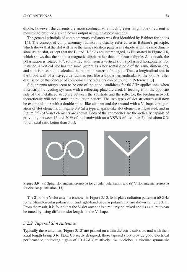
SLOT ANTENNAS 73
dipole, however, the currents are more confined, so a much greater magnitude of current isrequired to produce a given power output using the dipole antenna.
The general principle of complementary radiators was first identified by Babinet for optics[14]. The concept of complementary radiators is usually referred to as Babinet’s principle,which shows that the slot will have the same radiation pattern as a dipole with the same dimen-sions as the slot, except that the E- and H-fields are interchanged, as illustrated in Figure 3.8,which shows that the slot is a magnetic dipole rather than an electric dipole. As a result, thepolarisation is rotated 90◦, so that radiation from a vertical slot is polarised horizontally. Forinstance, a vertical slot has the same pattern as a horizontal dipole of the same dimensions,and so it is possible to calculate the radiation pattern of a dipole. Thus, a longitudinal slot inthe broad wall of a waveguide radiates just like a dipole perpendicular to the slot. A fullerdiscussion of the concept of complimentary radiators can be found in Reference [3].
Slot antenna arrays seem to be one of the good candidates for 60 GHz applications whenmicrostripline feeding systems with a reflecting plate are used. If feeding is on the oppositeside of the metallised structure between the substrate and the reflector, the feeding networktheoretically will not disturb the radiation pattern. The two types of slot structures will nowbe examined; one with a double spiral-like element and the second with a V-shape configur-ation of slot elements. In Figure 3.9 (a) a typical spiral-like slot element is illustrated, and inFigure 3.9 (b) V-slot elements are shown. Both of the approaches are theoretically capable ofproviding between 15 and 20 % of the bandwidth (at a VSWR of less than 2), and about 8 %for an axial ratio better than 3 dB.
Figure 3.9 (a) Spiral slot antenna prototype for circular polarisation and (b) V-slot antenna prototypefor circular polarisation [15]
The S11 of the V-slot antenna is shown in Figure 3.10. Its E-plane radiation pattern at 60 GHzfor left-hand circular polarisation and right-hand circular polarisation are shown in Figure 3.11.From the result, it is found that the V-slot antenna is circularly polarised and its axial ratio canbe tuned by using different slot lengths in the V shape.
3.2.2 Tapered Slot Antennas
Typically these antennas (Figure 3.12) are printed on a thin dielectric substrate and with theiraxial length being 3 to 12λ0. Correctly designed, these tapered slots provide good electricalperformance, including a gain of 10–17 dB, relatively low sidelobes, a circular symmetric
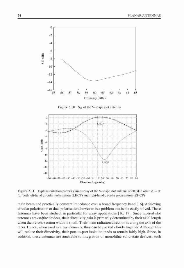
74 PLANAR ANTENNAS
–16
–14
–12
–10
–8
–6
–4
–2
0
55 56 57 58 59 60 61 62 63 64 65
Frequency (GHz)
S11
(dB
)
Figure 3.10 S11 of the V-shape slot antenna
–90
–16
–14
–12
–10
–8
–6
–4
–2
0
2
–80 –70 –60 –50 –40 –30 –20 –10 0 10 20 30 40 50 60 70 80 90
Elevation Angle (deg)
Gai
n (d
Bi)
LHCP
RHCP
Figure 3.11 E-plane radiation pattern gain display of the V-shape slot antenna at 60 GHz when φ = 0◦
for both left-hand circular polarisation (LHCP) and right-hand circular polarisation (RHCP)
main beam and practically constant impedance over a broad frequency band [16]. Achievingcircular polarisation or dual polarisation, however, is a problem that is not easily solved. Theseantennas have been studied, in particular for array applications [16, 17]. Since tapered slotantennas are endfire devices, their directivity gain is primarily determined by their axial lengthwhen their cross-section width is small. Their main radiation direction is along the axis of thetaper. Hence, when used as array elements, they can be packed closely together. Although thiswill reduce their directivity, their port-to-port isolation tends to remain fairly high. Since, inaddition, these antennas are amenable to integration of monolithic solid-state devices, such
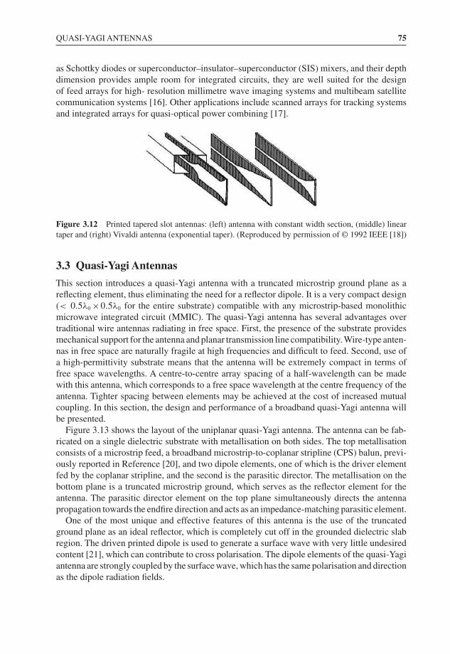
QUASI-YAGI ANTENNAS 75
as Schottky diodes or superconductor–insulator–superconductor (SIS) mixers, and their depthdimension provides ample room for integrated circuits, they are well suited for the designof feed arrays for high- resolution millimetre wave imaging systems and multibeam satellitecommunication systems [16]. Other applications include scanned arrays for tracking systemsand integrated arrays for quasi-optical power combining [17].
Figure 3.12 Printed tapered slot antennas: (left) antenna with constant width section, (middle) lineartaper and (right) Vivaldi antenna (exponential taper). (Reproduced by permission of © 1992 IEEE [18])
3.3 Quasi-Yagi Antennas
This section introduces a quasi-Yagi antenna with a truncated microstrip ground plane as areflecting element, thus eliminating the need for a reflector dipole. It is a very compact design(< 0.5λ0 ×0.5λ0 for the entire substrate) compatible with any microstrip-based monolithicmicrowave integrated circuit (MMIC). The quasi-Yagi antenna has several advantages overtraditional wire antennas radiating in free space. First, the presence of the substrate providesmechanical support for the antenna and planar transmission line compatibility. Wire-type anten-nas in free space are naturally fragile at high frequencies and difficult to feed. Second, use ofa high-permittivity substrate means that the antenna will be extremely compact in terms offree space wavelengths. A centre-to-centre array spacing of a half-wavelength can be madewith this antenna, which corresponds to a free space wavelength at the centre frequency of theantenna. Tighter spacing between elements may be achieved at the cost of increased mutualcoupling. In this section, the design and performance of a broadband quasi-Yagi antenna willbe presented.
Figure 3.13 shows the layout of the uniplanar quasi-Yagi antenna. The antenna can be fab-ricated on a single dielectric substrate with metallisation on both sides. The top metallisationconsists of a microstrip feed, a broadband microstrip-to-coplanar stripline (CPS) balun, previ-ously reported in Reference [20], and two dipole elements, one of which is the driver elementfed by the coplanar stripline, and the second is the parasitic director. The metallisation on thebottom plane is a truncated microstrip ground, which serves as the reflector element for theantenna. The parasitic director element on the top plane simultaneously directs the antennapropagation towards the endfire direction and acts as an impedance-matching parasitic element.
One of the most unique and effective features of this antenna is the use of the truncatedground plane as an ideal reflector, which is completely cut off in the grounded dielectric slabregion. The driven printed dipole is used to generate a surface wave with very little undesiredcontent [21], which can contribute to cross polarisation. The dipole elements of the quasi-Yagiantenna are strongly coupled by the surface wave, which has the same polarisation and directionas the dipole radiation fields.
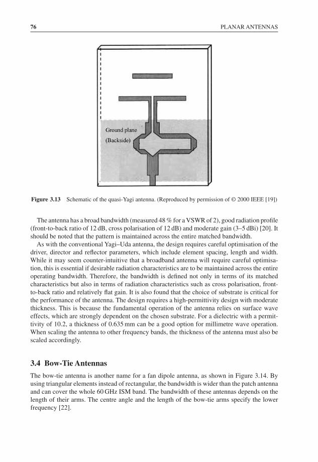
76 PLANAR ANTENNAS
Figure 3.13 Schematic of the quasi-Yagi antenna. (Reproduced by permission of © 2000 IEEE [19])
The antenna has a broad bandwidth (measured 48 % for a VSWR of 2), good radiation profile(front-to-back ratio of 12 dB, cross polarisation of 12 dB) and moderate gain (3–5 dBi) [20]. Itshould be noted that the pattern is maintained across the entire matched bandwidth.
As with the conventional Yagi–Uda antenna, the design requires careful optimisation of thedriver, director and reflector parameters, which include element spacing, length and width.While it may seem counter-intuitive that a broadband antenna will require careful optimisa-tion, this is essential if desirable radiation characteristics are to be maintained across the entireoperating bandwidth. Therefore, the bandwidth is defined not only in terms of its matchedcharacteristics but also in terms of radiation characteristics such as cross polarisation, front-to-back ratio and relatively flat gain. It is also found that the choice of substrate is critical forthe performance of the antenna. The design requires a high-permittivity design with moderatethickness. This is because the fundamental operation of the antenna relies on surface waveeffects, which are strongly dependent on the chosen substrate. For a dielectric with a permit-tivity of 10.2, a thickness of 0.635 mm can be a good option for millimetre wave operation.When scaling the antenna to other frequency bands, the thickness of the antenna must also bescaled accordingly.
3.4 Bow-Tie Antennas
The bow-tie antenna is another name for a fan dipole antenna, as shown in Figure 3.14. Byusing triangular elements instead of rectangular, the bandwidth is wider than the patch antennaand can cover the whole 60 GHz ISM band. The bandwidth of these antennas depends on thelength of their arms. The centre angle and the length of the bow-tie arms specify the lowerfrequency [22].
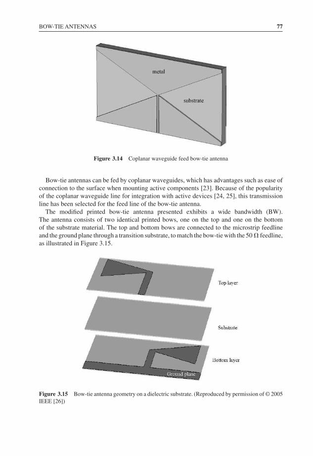
BOW-TIE ANTENNAS 77
Figure 3.14 Coplanar waveguide feed bow-tie antenna
Bow-tie antennas can be fed by coplanar waveguides, which has advantages such as ease ofconnection to the surface when mounting active components [23]. Because of the popularityof the coplanar waveguide line for integration with active devices [24, 25], this transmissionline has been selected for the feed line of the bow-tie antenna.
The modified printed bow-tie antenna presented exhibits a wide bandwidth (BW).The antenna consists of two identical printed bows, one on the top and one on the bottomof the substrate material. The top and bottom bows are connected to the microstrip feedlineand the ground plane through a transition substrate, to match the bow-tie with the 50 � feedline,as illustrated in Figure 3.15.
Figure 3.15 Bow-tie antenna geometry on a dielectric substrate. (Reproduced by permission of © 2005IEEE [26])
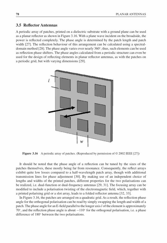
78 PLANAR ANTENNAS
3.5 Reflector Antennas
A periodic array of patches, printed on a dielectric substrate with a ground plane can be usedas a planar reflector as shown in Figure 3.16. With a plane wave incident on the broadside, thepower is reflected completely. The phase angle is determined by the patch length and patchwidth [27]. The reflection behaviour of this arrangement can be calculated using a spectral-domain method [28]. The phase angle varies over nearly 360◦; thus, such elements can be usedas reflection phase shifters. The phase angles calculated from a periodic structure can even beused for the design of reflecting elements in planar reflector antennas, as with the patches ona periodic grid, but with varying dimensions [29].
Figure 3.16 A periodic array of patches. (Reproduced by permission of © 2002 IEEE [27])
It should be noted that the phase angle of a reflection can be tuned by the sizes of thepatches themselves, these mostly being far from resonance. Consequently, the reflect arraysexhibit quite low losses compared to a half-wavelength patch array, though with additionaltransmission lines for phase adjustment [30]. By making use of an independent choice oflengths and widths of the printed patches, different properties for the two polarisations canbe realized, i.e. dual-function or dual-frequency antennas [29, 31]. The focusing array can bemodified to include a polarisation twisting of the electromagnetic field, which, together witha printed polarising grid or a slot array, leads to a folded reflector antenna [32, 33].
In Figure 3.16, the patches are arranged on a quadratic grid. As a result, the reflection phaseangle for the orthogonal polarisation can be read by simply swapping the length and width of apatch. The phase angle for an E-field parallel to the longer axis l of the element is approximately70◦, and the reflection phase angle is about −110◦ for the orthogonal polarisation, i.e. a phasedifference of 180◦ between the two polarisations.
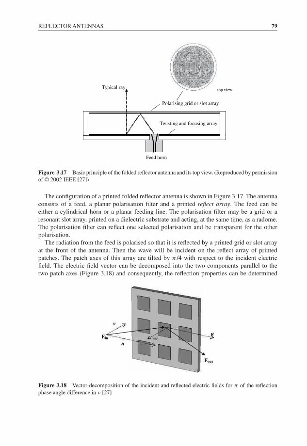
REFLECTOR ANTENNAS 79
top view
Polarising grid or slot array
Twisting and focusing array
Feed horn
Typical ray
Figure 3.17 Basic principle of the folded reflector antenna and its top view. (Reproduced by permissionof © 2002 IEEE [27])
The configuration of a printed folded reflector antenna is shown in Figure 3.17. The antennaconsists of a feed, a planar polarisation filter and a printed reflect array. The feed can beeither a cylindrical horn or a planar feeding line. The polarisation filter may be a grid or aresonant slot array, printed on a dielectric substrate and acting, at the same time, as a radome.The polarisation filter can reflect one selected polarisation and be transparent for the otherpolarisation.
The radiation from the feed is polarised so that it is reflected by a printed grid or slot arrayat the front of the antenna. Then the wave will be incident on the reflect array of printedpatches. The patch axes of this array are tilted by π /4 with respect to the incident electricfield. The electric field vector can be decomposed into the two components parallel to thetwo patch axes (Figure 3.18) and consequently, the reflection properties can be determined
Figure 3.18 Vector decomposition of the incident and reflected electric fields for π of the reflectionphase angle difference in ν [27]
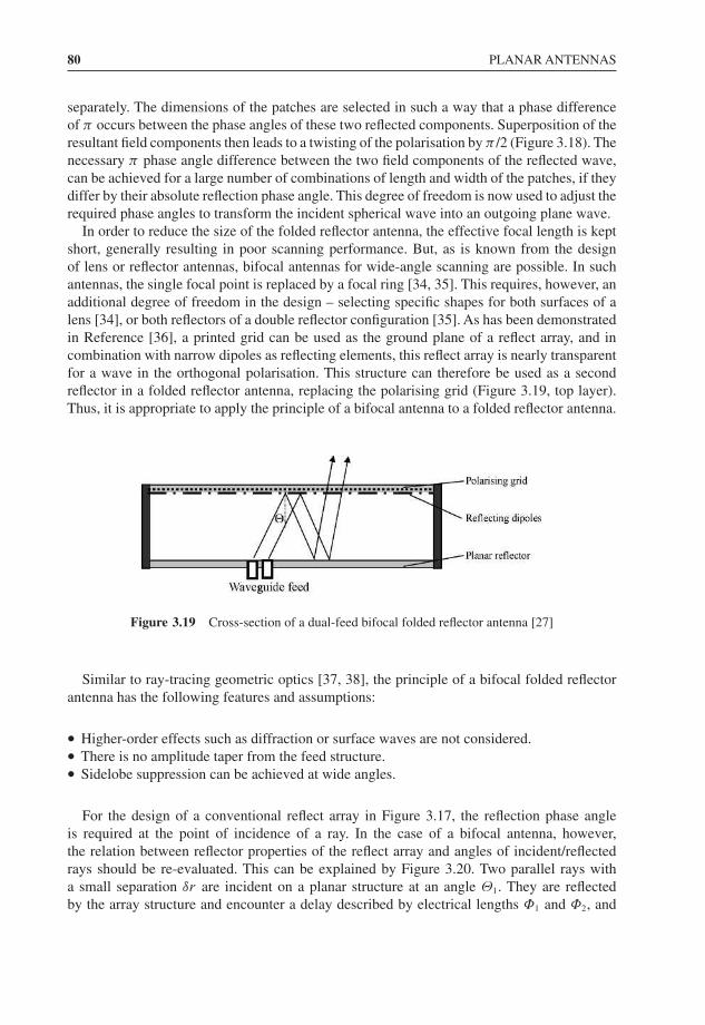
80 PLANAR ANTENNAS
separately. The dimensions of the patches are selected in such a way that a phase differenceof π occurs between the phase angles of these two reflected components. Superposition of theresultant field components then leads to a twisting of the polarisation by π /2 (Figure 3.18). Thenecessary π phase angle difference between the two field components of the reflected wave,can be achieved for a large number of combinations of length and width of the patches, if theydiffer by their absolute reflection phase angle. This degree of freedom is now used to adjust therequired phase angles to transform the incident spherical wave into an outgoing plane wave.
In order to reduce the size of the folded reflector antenna, the effective focal length is keptshort, generally resulting in poor scanning performance. But, as is known from the designof lens or reflector antennas, bifocal antennas for wide-angle scanning are possible. In suchantennas, the single focal point is replaced by a focal ring [34, 35]. This requires, however, anadditional degree of freedom in the design – selecting specific shapes for both surfaces of alens [34], or both reflectors of a double reflector configuration [35]. As has been demonstratedin Reference [36], a printed grid can be used as the ground plane of a reflect array, and incombination with narrow dipoles as reflecting elements, this reflect array is nearly transparentfor a wave in the orthogonal polarisation. This structure can therefore be used as a secondreflector in a folded reflector antenna, replacing the polarising grid (Figure 3.19, top layer).Thus, it is appropriate to apply the principle of a bifocal antenna to a folded reflector antenna.
Figure 3.19 Cross-section of a dual-feed bifocal folded reflector antenna [27]
Similar to ray-tracing geometric optics [37, 38], the principle of a bifocal folded reflectorantenna has the following features and assumptions:
• Higher-order effects such as diffraction or surface waves are not considered.• There is no amplitude taper from the feed structure.• Sidelobe suppression can be achieved at wide angles.
For the design of a conventional reflect array in Figure 3.17, the reflection phase angleis required at the point of incidence of a ray. In the case of a bifocal antenna, however,the relation between reflector properties of the reflect array and angles of incident/reflectedrays should be re-evaluated. This can be explained by Figure 3.20. Two parallel rays witha small separation δr are incident on a planar structure at an angle Θ1. They are reflectedby the array structure and encounter a delay described by electrical lengths Φ1 and Φ2, and
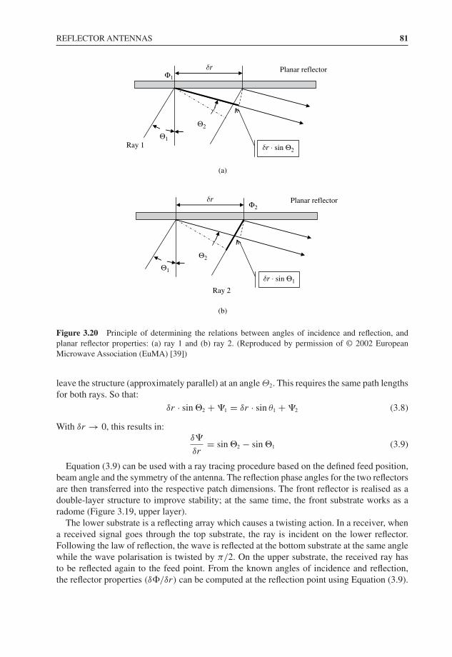
REFLECTOR ANTENNAS 81
(a)
(b)
Θ1
Θ2
Φ2
Ray 2
Θ1
Θ2
δ rΦ1
Ray 1
Planar reflector
Planar reflector
δ r ⋅ sin Θ2
δ r ⋅ sin Θ1
δ r
Figure 3.20 Principle of determining the relations between angles of incidence and reflection, andplanar reflector properties: (a) ray 1 and (b) ray 2. (Reproduced by permission of © 2002 EuropeanMicrowave Association (EuMA) [39])
leave the structure (approximately parallel) at an angle Θ2. This requires the same path lengthsfor both rays. So that:
δr · sin �2 + �1 = δr · sin θ1 + �2 (3.8)
With δr → 0, this results in:δ�
δr= sin �2 − sin �1 (3.9)
Equation (3.9) can be used with a ray tracing procedure based on the defined feed position,beam angle and the symmetry of the antenna. The reflection phase angles for the two reflectorsare then transferred into the respective patch dimensions. The front reflector is realised as adouble-layer structure to improve stability; at the same time, the front substrate works as aradome (Figure 3.19, upper layer).
The lower substrate is a reflecting array which causes a twisting action. In a receiver, whena received signal goes through the top substrate, the ray is incident on the lower reflector.Following the law of reflection, the wave is reflected at the bottom substrate at the same anglewhile the wave polarisation is twisted by π/2. On the upper substrate, the received ray hasto be reflected again to the feed point. From the known angles of incidence and reflection,the reflector properties (δ�/δr) can be computed at the reflection point using Equation (3.9).
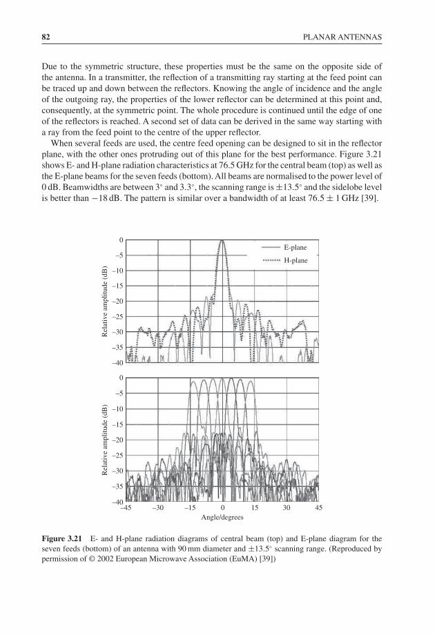
82 PLANAR ANTENNAS
Due to the symmetric structure, these properties must be the same on the opposite side ofthe antenna. In a transmitter, the reflection of a transmitting ray starting at the feed point canbe traced up and down between the reflectors. Knowing the angle of incidence and the angleof the outgoing ray, the properties of the lower reflector can be determined at this point and,consequently, at the symmetric point. The whole procedure is continued until the edge of oneof the reflectors is reached. A second set of data can be derived in the same way starting witha ray from the feed point to the centre of the upper reflector.
When several feeds are used, the centre feed opening can be designed to sit in the reflectorplane, with the other ones protruding out of this plane for the best performance. Figure 3.21shows E- and H-plane radiation characteristics at 76.5 GHz for the central beam (top) as well asthe E-plane beams for the seven feeds (bottom). All beams are normalised to the power level of0 dB. Beamwidths are between 3◦ and 3.3◦, the scanning range is ±13.5◦ and the sidelobe levelis better than −18 dB. The pattern is similar over a bandwidth of at least 76.5 ± 1 GHz [39].
–45–40
–35
–30
–25
–20
–15
–10
–5
0
–30 –15 0 15 30 45Angle/degrees
E-plane
H-plane
Rel
ativ
e am
plitu
de (
dB)
–40
–35
–30
–25
–20
–15
–10
–5
0
Rel
ativ
e am
plitu
de (
dB)
Figure 3.21 E- and H-plane radiation diagrams of central beam (top) and E-plane diagram for theseven feeds (bottom) of an antenna with 90 mm diameter and ±13.5◦ scanning range. (Reproduced bypermission of © 2002 European Microwave Association (EuMA) [39])
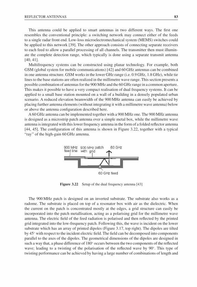
REFLECTOR ANTENNAS 83
This antenna could be applied to smart antennas in two different ways. The first oneresembles the conventional principle: a switching network may connect either of the feedsto a single radar front end. Low-loss microelectromechanical system (MEMS) switches couldbe applied to this network [39]. The other approach consists of connecting separate receiversto each feed to allow a parallel processing of all channels. The transmitter then must illumin-ate the complete detection range, which typically is done using a separate transmit antenna[40, 41].
Multifrequency systems can be constructed using planar technology. For example, bothGSM (global system for mobile communications) [42] and 60 GHz antennas can be combinedin one antenna structure. GSM works in the lower GHz range (i.e. 0.9 GHz, 1.8 GHz), while tielines to the base stations are often realized in the millimetre wave range. This section presents apossible combination of antennas for the 900 MHz and the 60 GHz range in a common aperture.This makes it possible to have a very compact realisation of dual frequency systems. It can beapplied to a small base station mounted on a wall of a building in a densely populated urbanscenario. A reduced elevation beamwidth of the 900 MHz antenna can easily be achieved byplacing further antenna elements (without integrating it with a millimetre wave antenna) belowor above the antenna configuration described here.
A 60 GHz antenna can be implemented together with a 900 MHz one. The 900 MHz antennais designed as a microstrip patch antenna over a simple metal box, while the millimetre waveantenna is integrated with this lower frequency antenna in the form of a folded reflector antenna[44, 45]. The configuration of this antenna is shown in Figure 3.22, together with a typical“ray’’ of the high-gain 60 GHz antenna.
Figure 3.22 Setup of the dual frequency antenna [43]
The 900 MHz patch is designed on an inverted substrate. The substrate also works as aradome. The substrate is placed on top of a resonator box with air as the dielectric. Whenthe current on the patch is concentrated mostly at the edges, a grid structure can easily beincorporated into the patch metallisation, acting as a polarising grid for the millimetre waveantenna. The electric field of the feed radiation is polarised and then reflected by the printedgrid integrated into the low-frequency patch. Following this, the wave is incident on the lowersubstrate which has an array of printed dipoles (Figure 3.17, top right). The dipoles are tiltedby 45◦ with respect to the incident electric field. The field can be decomposed into componentsparallel to the axes of the dipoles. The geometrical dimensions of the dipoles are designed insuch a way that, a phase difference of 180◦ occurs between the two components of the reflectedwave; leading to a twisting of the polarisation of the reflected wave by 90◦. This type oftwisting performance can be achieved by having a large number of combinations of length and
84 PLANAR ANTENNAS
width dipoles, which differ only by the absolute reflection phase angle. This overall phaseshift is adjusted according to the focusing requirements. The original concept of this antennais based on periodic structures using spectral domain calculations.
Such multiband antennas cover the mobile communication frequency band around 900 MHzand the communication band at 60 GHz, together with the ISM band around 61 GHz. The900 MHz antenna is based on a resonator-backed microstrip patch antenna, while the millimetrewave antenna consists of a folded reflector antenna with a polarising grid integrated intothe antenna patch; and a twisting and focusing planar reflector placed on the bottom of the900 MHz antenna box. This configuration could be an antenna solution for GSM and 60 GHzaccess points.
3.6 Millimetre Wave Design Considerations
In millimetre waves, the thickness of the dielectric between the patch or patch stack and theground plane has a strong influence on the bandwidth of the antenna [46] and, consistently,the simulations and measurements show a wider impedance bandwidth for the circular single-element (Figure 3.3 (a)) than the stacked two-element patch antenna (Figure 3.7 (c)) [47].
The diameter of the patch can be designed to be 890 �m with the silver paste spreadingcausing an extra 60 �m in patch diameter. This explains why the observed centre frequencyspots are sometimes detuned below 60 GHz. The 25-�m-shifted feed point position corrects,to some degree, the effect of the increased realised patch size.
The spreading of the silver paste during the firing stage of the low-temperature co-firedceramics (LTCC) (see Chapter 9) [48] processing, has occurred quite often with the FerroA6-S materials [49]. It is difficult to predict how much the spreading will be compensated bythe layout design in each case. However, research work shows that gold paste of the FerroA6-S system does not practically spread at all, and hence it is the preferred choice for thesetypes of applications.
The transition can be designed using a coupling slot with the coplanar waveguide line, asshown in Figure 3.23. In general, a slot transition cannot be used if wideband functioning isdesired, but in this particular case this is not regarded as a problem. The design of the slottransition is quite simple. The width of the slot is selected so that its realisation in the LTCCprocess is feasible. For this implementation 150 �m is considered reasonable. The length of theslot from end to end is close to the corresponding electrical half-wavelength in the dielectricmedium used, which is about 1.0 mm in this case. Both the coplanar waveguide and SLcontinueslightly over the slot region, and hence form two stubs in the transition. The exact dimensionsof the slot and the stubs can be calculated using a simulator, to give the desired trade-offbetween adequate return loss and band width. For this transition, the simulated return loss isabout −39 dB and the insertion loss is close to −0.62 dB at 60 GHz. The impedance matchingbandwidth for the return loss of at least −15 dB is in the range of 54–66 GHz.
The minimum insertion loss for a single transition seems to be 1.1 dB, though the S11 andS22 may have different frequency responses if there is a variation in the physical dimensionscompared to the realised conductor patterns; which will cause some asymmetry [50]. Des-pite the deteriorated performance caused by the dimensional tolerances, the functioning ofthe transition can be regarded as adequate to achieve the aimed for antenna radiation gainmeasurements.
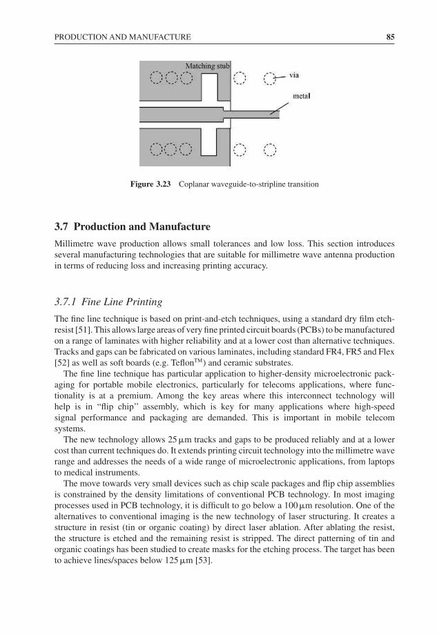
PRODUCTION AND MANUFACTURE 85
Figure 3.23 Coplanar waveguide-to-stripline transition
3.7 Production and Manufacture
Millimetre wave production allows small tolerances and low loss. This section introducesseveral manufacturing technologies that are suitable for millimetre wave antenna productionin terms of reducing loss and increasing printing accuracy.
3.7.1 Fine Line Printing
The fine line technique is based on print-and-etch techniques, using a standard dry film etch-resist [51]. This allows large areas of very fine printed circuit boards (PCBs) to be manufacturedon a range of laminates with higher reliability and at a lower cost than alternative techniques.Tracks and gaps can be fabricated on various laminates, including standard FR4, FR5 and Flex[52] as well as soft boards (e.g. TeflonTM) and ceramic substrates.
The fine line technique has particular application to higher-density microelectronic pack-aging for portable mobile electronics, particularly for telecoms applications, where func-tionality is at a premium. Among the key areas where this interconnect technology willhelp is in “flip chip’’ assembly, which is key for many applications where high-speedsignal performance and packaging are demanded. This is important in mobile telecomsystems.
The new technology allows 25 �m tracks and gaps to be produced reliably and at a lowercost than current techniques do. It extends printing circuit technology into the millimetre waverange and addresses the needs of a wide range of microelectronic applications, from laptopsto medical instruments.
The move towards very small devices such as chip scale packages and flip chip assembliesis constrained by the density limitations of conventional PCB technology. In most imagingprocesses used in PCB technology, it is difficult to go below a 100 �m resolution. One of thealternatives to conventional imaging is the new technology of laser structuring. It creates astructure in resist (tin or organic coating) by direct laser ablation. After ablating the resist,the structure is etched and the remaining resist is stripped. The direct patterning of tin andorganic coatings has been studied to create masks for the etching process. The target has beento achieve lines/spaces below 125 �m [53].
86 PLANAR ANTENNAS
3.7.2 Thick Film
Millimetre wave circuitry requires high-resolution etching technology, and its functional dens-ity is increasing. It is common to use ceramic materials, which include thick-film conductorson aluminates and circuits using Green TapeTM low-temperature co-fired ceramics [48]. Con-ductor patterning techniques include conventional screen printing, Fodel® photoimaging andetching processes. Thin-film depositions have also been considered since this has been themost viable technology from which to fabricate millimetre wave circuits [51].
It is important to note that the fabrication of millimetre wave circuits requires close col-laboration with the designer, from circuit layout to final productions, because of the specialgeometries required for: transmit and receive lines, for waveguides, to limit reflection andpropagation losses, as well as for the construction of specific components, such as antennas,couplers and dividers.
Since the mid-1990s, more opportunities have arisen for the use of ceramic circuitries inhigh-frequency modules; with more information available on their performance in the milli-metre wave range and new materials on offer, including LTCC and FODEL® photodefinableconductors [54].
3.7.3 Thin Film
Thin-film technology has been the traditional method used to manufacture microwave circuitryfor many years.With outstanding line resolution, excellent conductor edge definition, combinedwith superb ceramic substrate properties at high frequency and stable thermal behaviour; whichare all ideal attributes of circuitry for use in portable devices. However, this approach hasdisadvantages in terms of cost. Complex modules are often assembled in a special hermetichousing using a patchwork arrangement of certain substrates. The major reason used to dividethe circuit into subcircuits is related to the yield figures obtained on large substrates. Positioningaccuracy of these substrates is crucial to avoid gaps and related impedance changes. Thehousing itself needs to have expensive hermetic RF interconnections. Multilayer substratesbased on LTCC [48] offer a variety of options for microwave designs. DC connections anddigital control functions can be implemented in separate layers, chip tailored cavities can beused to improve the return loss of the signal interconnections, various transmission line typesas well as waveguides are available; and the hermetic substrate itself can be used as part ofthe package with integrated feedthroughs. Embedded resistors and capacitors are additionalfeatures which will further shrink the size of designs. However, fine line printing resolution andassociated tolerances may well be the restricting factors in minimizing design size. Althoughlines and spaces down to 50 �m are achievable, this is not sufficient for certain elements likeedge coupled filters, couplers, etc.
A recent approach, FINEBRID, combining the advantages of both technologies, wasdeveloped and evaluated within a funded program [51]. Thin-film structures were appliedon fired LTCC substrates without special surface treatment. This process allows a combinationof printed thick-film and thin-film structures on the surface. Hence, the combined technologyoffers improved technology features such as smaller lines and spaces. Thin-film features canbe reduced to the necessary areas, and special thick-film materials for hermetic sealing can beapplied, thus providing options to reduce cost, size and weight.
REFERENCES 87
3.7.4 System-on-Chip
Increasing demand for low-cost, broadband, high-speed and small wireless communicationdevices, especially in the millimetre wave frequency range, has turned the SoC (system-on-chip) solution into an important technique to satisfy these demands [55]. One of the mostimportant problems in the performance of on-chip antennas in the millimetre wave range issubstrate losses. By using micromachining techniques [56], it is possible to remove unwantedregions of the substrate and thus reduce substrate losses.
In the example of silicon technology, (100) silicon substrates with a thickness of 550 �mare typically used for the realisation of on-chip antennas [56]. The fabrication of devicesrequires two steps of back- and front-side processing. The back-side etching is performed ina KOH (potassium hydroxide) solution of a concentration of 8 moles, and at a temperature of52–58 ◦C. During this step, silicon is removed through the openings in the masking layerfor a period of 25–30 hours. Since the etching step is rather extended, it is important that themasking layer can withstand long exposures to etching chemicals. Thus it can be seen that thereare a number of fabrication technologies available. Each has its advantages and drawbacks.However, the final application will determine the choice of process.
References[1] N. G.Alexopoulos and I. E. Rana, ‘Mutual Impedance Computation between Printed Dipoles’, IEEE Transactions
on Antennas and Propagation, AP-29, January 1981, 106–111.[2] R. S. Elliot and G.. I. Stem, ‘The Design of Microstrip Dipole Arrays Including Mutual Coupling, Part 1: Theory;
Part 11: Experiment’, IEEE Transactions on Antennas and Propagation, AP-29, September 1981, 757–765.[3] D. Pozar, ‘Considerations for Millimetre Wave Printed Antennas’, IEEE Transactions on Antennas and
Propagation, 31(5), September 1983, 740–747.[4] K. R. Carver and J. W. Mink, ‘MicrostripAntenna Technology’, IEEE Transactions on Antennas and Propagation,
AP-29, January 1981, 2–24.[5] R. F. Harrington, ‘Time-Harmonic Electromagnetic Fields’, McGraw-Hill, New York, 1961.[6] Rogers Corporation website, http://www.rogerscorporation.com/[7] DuPont Microcircuit Material website, http://www.dupont.com/mcm/[8] Dielectric Chart, Emerson and Cuming Microwave Products, Massachusetts.[9] K. S. Yngvesson, T. L. Korzeniowski, R. H. Mathews, P. T. Parrish and T. C. L. G. Sollner, ‘Plane Millimetre Wave
Antennas with Application to Monolithic Receivers’, Proceedings of SPIE, 337 (Milli-meter Wave Technology),1982.
[10] M. Irsadi Aksun, Shun-lien Chuang et al., ‘On Slot-Coupled Microstrip Antennas and Their Applications to CPOperation – Theory and Experiment’, IEEE Transactions on Antennas and Propagation, 38(8), August 1990,1224–1230.
[11] O. Lafond, M. Himdi and J. P. Daniel, ‘Aperture Coupled Microstrip Patch Antenna with a Thick Ground Planein Millimetre Waves’, IEE Electronics Letters, 35(17), August 1999, 1394–1396.
[12] W. S. T. Rowe and R. B. Waterhouse, ‘Broadband Coplanar-Waveguide Fed Stacked Patch Antenna’, ElectronicsLetters, 35(9), 1999, 681–682.
[13] David Pozar, ‘Microstrip Antennas’, Proceedings of IEEE, 80(1), January 1992, 79–91.[14] Wikipedia,‘Babinet’s_Principle’, http://en.wikipedia.org/wiki/Babinet’s_principle.[15] Gerald Oberschmidt, Veselin Brankovic and Dragan Krupezevic, ‘V-Slot Antenna for Circular Polarization’, US
Patent 2002000943.[16] K. S. Yngvesson, D. H. Schaubert, T. L. Korzeniowski, E. L. Kollberg, T. Thungren and J. F. Johansson, ‘Endfire
Tapered Slot Antennas on Dielectric Substrates’, IEEE Transactions on Antennas and Propagation, AP-33,December 1985, 1392–1400.
[17] K. S.Yngvesson et al., ‘The Tapered SlotAntenna-ANew Integrated Element for Millimetre-WaveApplications’,IEEE Transactions on Microwave Theory and Technology, 37, February 1989, 365–374.
[18] Felix K. Schwering,’Millimetre Wave Antennas’, Proceedings of the IEEE, 80(1), January 1992, 92–102.

88 PLANAR ANTENNAS
[19] William R. Deal, Noriaki Kaneda (Student), James Sor,Yongxi Qian and Tatsuo Itoh, ‘ANew Quasi-YagiAntennafor Planar Active Antenna Arrays’, IEEE Transactions on Microwave Theory and Techniques, 48(6), June 2000,910–918.
[20] Y. Qian and T. Itoh, ‘A Broadband Uniplanar Microstrip-to-CPS Transition’, Asia–Pacific Microwave Con-ference Digest, December 1997, 609–612.
[21] N. G. Alexopoulos, P. B. Ketehi and D. B. Rutledge, ‘Substrate optimization for integrated circuit antennas’,IEEE Transactions on Microwave Theory and Techniques, MTT-31, July 1983, 550–557.
[22] I. Oppermann, M. Hämäläinen and J. Iinatti, ‘UWB: Theory and Applications’, John Wiley & Sons, Ltd,Chichester, September 2004.
[23] R. N. Simons, ‘Coplanar Waveguide Circuits, Components, and Systems’, John Wiley & Sons, Inc., New York,2001.
[24] Hojr Sedaghat-Pisheh1, Mahmoud Shahabadi 2 and Shamsodin Mohajerzadeh 1, ‘Design, Simulation, andFabrication of an On-Chip Antenna Fabricated Using Silicon Micromachining for Broad-Band Millimetre-WaveWireless Communications’, Proceedings of the 36th European Microwave Conference, 2006.
[25] V. K. Varadan, K. J. Vinoy and K. A. Jose, ‘RF MEMS and Their Applications’, John Wiley and Sons, Ltd,Chichester, December 2002.
[26] Abdelnasser A. Eldek, Atef Z. Elsherbeni, ‘A Microstrip-Fed Modified Printed Bow-Tie Antenna for Simultan-eous Operation in the C and X-Bands’, IEEE International Radar Conference, May 2005, pp. 939–943.
[27] W. Menzel, D. Pilz and M. Al-Tikriti, ‘Millimetre-Wave Folded Reflector Antennas with High Gain, Low Loss,and Low Profile’, IEEE Antennas and Propagation Magazine, 44(3), June 2002, 24–29.
[28] R. Mittra et al., ‘Techniques for Analyzing Frequency Selective Surfaces – A Review’, Proceedings of the IEEE,76(12), December 1988, 1593–1615.
[29] D. M. Pozar, S. D. Targonski and H. D. Syrigos, ‘Design of Millimetre Wave Microstrip Reflectarrays’, IEEETransactions on Antennas and Propagation, AP-45, 1997, 287–296.
[30] R. D. Javor, X.-D. Wu and K. Chang, ‘Design and Performance of a Microstrip Flat Reflectarray Antenna’,Microwave and Optical Technology Letters, 7(7), 1994, 322–324.
[31] D. Pilz and W. Menzel, ‘Periodic and Quasi-Periodic Structures for Antenna Applications’, Proceedings of the29th European Microwave Conference, Vol. III, Munich, Germany, 1999, pp. 311–314.
[32] W. Menzel, D. Pilz and R. Leberer, ‘A 77 GHz FM/CW Radar Front-End with a Low-Profile, Low-Loss PrintedAntenna’, IEEE Transactions on Microwave Theory and Techniques, MTT-47(12), December 1999, 2237–2241.
[33] W. Menzel and D. Pilz, ‘Printed Quasi-Optical Wave Antennas’, Millennium Conference on ‘Antennas andPropagation’, AP2000, Davos, Switzerland, 2000, Session 3A2-1, Paper 0023.
[34] P. S. Holt and A. Mayer, ‘A Design Procedure for Dielectric Microwave Lenses of Large Aperture Ratio andLarge Scanning Angle’, IRE Transactions on Antennas and Propagation, AP-5, 1957, 25–30.
[35] A. Y. Niazi and P. J. Mitchell, ‘Millimetre Wave Phase Corrected Reflector Antenna’, IEE InternationalConference on ‘Antennas and Propagation’, ICAP’83, Norwich, England, April 1983, Part 1, pp. 51–54.
[36] W. Menzel and D. Pilz, ‘Printed mm-Wave Folded Reflector Antennas withHigh Gain, Low Loss, and LowProfile’, IEEE Antennas and Propagation Conference, Salt Lake City, Utah, July 2000, Vol. 2, pp. 790–793.
[37] P. S. Holt and A. Mayer, ‘A Design Procedure for Dielectric Microwave Lenses of Large Aperture Ratio andLarge Scanning Angle’, IRE Transactions on Antennas and Propagation, AP-5, 1957, 25–30.
[38] A.Y. Niazi and P. J. Mitchell, ‘Millimetre Wave Phase Corrected ReflectorAntenna, IEE International Conferenceon ‘Antennas and Propagation’, ICAP’83, Norwich, England, April 1983, Part 1, pp. 51–54.
[39] W. Menzel, M. Al-Tikriti and R. Leberer, ‘A 76 GHz Multiple-Beam Planar Reflector Antenna’, 34th EuropeanMicrowave Conference, 2002, pp. 1–4.
[40] C. Metz, E. Lissel and A. F. Jacob, ‘Planar Multiresolutional Antenna for Automotive Radar, 31st EuropeanMicrowave Conference, London, 2001, pp. 335–338.
[41] M. Younis, A. Herschlein, Y. J. Park and W. Wiesbeck, ‘A Parallel-Plate Luneburg Lens Sensor Concept forAutomatic Cruise Control Applications, 31st European Microwave Conference, London, 2001, pp. 339–342.
[42] Wikipedia, ‘GSM’, http://www.wikipedia.org/[43] Wolfgang Menzel, Maysoun Al-Tikriti and Maria Belen Espadas Lopez, ‘A Common Aperture, Dual Frequency
Printed Antenna (900 MHz and 60 GHz)’, Electronics Letters, 37(17), 16 August 2001, 1059–1060.[44] D. Pilz and W. Menzel, ‘Folded Reflectarray Antenna’, Electronics Letters, 34(9), April 1998, 832–833.[45] D. Pilz and W. Menzel, ‘Printed Millimetre-Wave Reflectarrays’ Annales de Telecommunications, 56(1–2),
2001, 2–11.

REFERENCES 89
[46] K. R. Carver and J. W. Mink, ‘MicrostripAntenna Technology’, IEEE Transactions on Antennas and Propagation,29, January 1981, 18–20.
[47] Antti Vimpari,Antti Lamminen and Jussi Säily, ‘Design and Measurements of 60 GHz Probe-Fed PatchAntennason Low-Temperature Co-fired Ceramic Substrates’, Proceedings of the 36th European Microwave Conference,2006, pp. 854–857.
[48] Wikipedia, ‘Low Temperature Co-fired Ceramics’, http://www.wikipedia.org/[49] Ferro, ‘LTCC A6 System for Wireless Solutions’, Ferro® Electronic Material.[50] Antti Vimpari, Antti Lamminen (2) and Jussi Säily, ‘Design and Measurements of 60 GHz Probe-Fed Patch
Antennas on Low-Temperature Co-fired Ceramic Substrates’, Proceedings of the 36th European MicrowaveConference, 2006.
[51] G. Vanrietvelde, E. Polzer, S. Nicotra, J. Mueller and A. Brokmeier, ‘Microwave and Millimeter Wave Applica-tions: A New Challenge for Ceramic Thick Film Technology’, IEE Seminar on ‘Microwave Thick Film Materialsand Circuits’, 2007, paper 2002/097, pp. 6–10.
[52] R. S. Khandpur, ‘Printed Circuit Boards’, McGraw-Hill Professional, September 2005.[53] W. Falinski, G. Koziol and J. Borecki, ‘Laser Structuring of Fine Line Printed Circuit Boards’, 28th International
Spring Seminar on ‘Electronics Technology: Meeting the Challenges of Electronics Technology Progress’, 19–20May 2005, pp. 196–201.
[54] DuPont Electronic Material Data Sheet, ‘Fodel® 6778 Conductor’, http://www.dupont.com/[55] Y. P. Zhang, ‘Recent Advances in Integration of Antenna on Silicon Chip and Ceramic Package’, IEEE
International Workshop on ‘Antenna Technology’, 2005, pp. 151–154.[56] Gildas P. Gauthier, Linda P. Katehi and Gabriel A. I. Rebeiz, ‘A 94 GHz Aperture-Coupled Micromachined
Microstrip Antenna’, IEEE MTT-S Digest, 1998, 993–996.

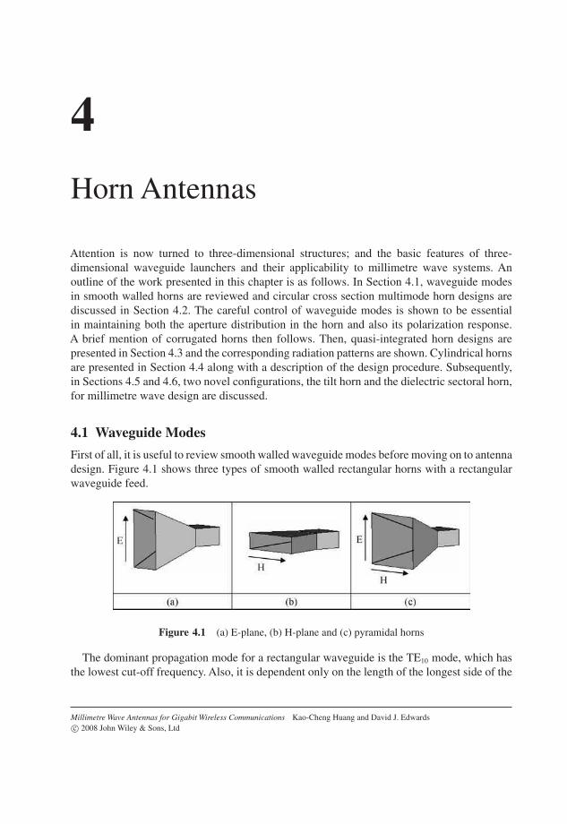
4Horn Antennas
Attention is now turned to three-dimensional structures; and the basic features of three-dimensional waveguide launchers and their applicability to millimetre wave systems. Anoutline of the work presented in this chapter is as follows. In Section 4.1, waveguide modesin smooth walled horns are reviewed and circular cross section multimode horn designs arediscussed in Section 4.2. The careful control of waveguide modes is shown to be essentialin maintaining both the aperture distribution in the horn and also its polarization response.A brief mention of corrugated horns then follows. Then, quasi-integrated horn designs arepresented in Section 4.3 and the corresponding radiation patterns are shown. Cylindrical hornsare presented in Section 4.4 along with a description of the design procedure. Subsequently,in Sections 4.5 and 4.6, two novel configurations, the tilt horn and the dielectric sectoral horn,for millimetre wave design are discussed.
4.1 Waveguide Modes
First of all, it is useful to review smooth walled waveguide modes before moving on to antennadesign. Figure 4.1 shows three types of smooth walled rectangular horns with a rectangularwaveguide feed.
Figure 4.1 (a) E-plane, (b) H-plane and (c) pyramidal horns
The dominant propagation mode for a rectangular waveguide is the TE10 mode, which hasthe lowest cut-off frequency. Also, it is dependent only on the length of the longest side of the
Millimetre Wave Antennas for Gigabit Wireless Communications Kao-Cheng Huang and David J. Edwardsc© 2008 John Wiley & Sons, Ltd
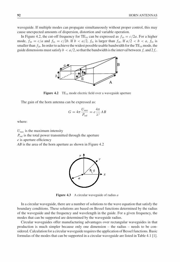
92 HORN ANTENNAS
waveguide. If multiple modes can propagate simultaneously without proper control, this maycause unexpected amounts of dispersion, distortion and variable operation.
In Figure 4.2, the cut-off frequency for TE10 can be expressed as f10 = c/2a. For a highermode, f20 = c/a and f01 = c/2b. If b < a/2, f01 is larger than f20. If a/2 < b < a, f01 issmaller than f20. In order to achieve the widest possible usable bandwidth for the TE10 mode, theguide dimensions must satisfy b < a/2, so that the bandwidth is the interval betweenfc and 2fc.
Figure 4.2 TE10 mode electric field over a waveguide aperture
The gain of the horn antenna can be expressed as:
G = 4πUmax
Prad
= e4π
λ2AB
where:
Umax is the maximum intensityPrad is the total power transmitted through the aperturee is aperture efficiencyAB is the area of the horn aperture as shown in Figure 4.2
Figure 4.3 A circular waveguide of radius a
In a circular waveguide, there are a number of solutions to the wave equation that satisfy theboundary conditions. These solutions are based on Bessel functions determined by the radiusof the waveguide and the frequency and wavelength in the guide. For a given frequency, themodes that can be supported are determined by the waveguide radius.
Circular waveguides offer manufacturing advantages over rectangular waveguides in thatproduction is much simpler because only one dimension – the radius – needs to be con-sidered. Calculation for a circular waveguide requires the application of Bessel functions. Basicformulas of the modes that can be supported in a circular waveguide are listed in Table 4.1 [1].
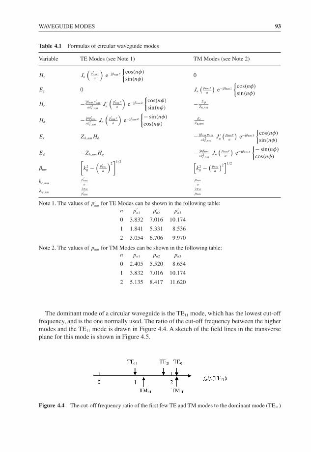
WAVEGUIDE MODES 93
Table 4.1 Formulas of circular waveguide modes
Variable TE Modes (see Note 1) TM Modes (see Note 2)
Hz Jn
(p′nmr
a
)e−jβnmz
{cos(nφ)
sin(nφ)0
Ez 0 Jn
(pnmr
a
)e−jβnmz
{cos(nφ)
sin(nφ)
Hr − jβnmp′nm
ak2c,nm
J ′n
(p′nmr
a
)e−jβnmz
{cos(nφ)
sin(nφ)− Eφ
Ze,nm
Hφ − jnp′nm
rk2c,nm
Jn
(p′nmr
a
)e−jβnmz
{− sin(nφ)
cos(nφ)Er
Ze,nm
Er Zh,nmHφ − jβnmpnm
ak2c,nm
J ′n
(pnmr
a
)e−jβnmz
{cos(nφ)
sin(nφ)
Eφ −Zh,nmHρ − jnβnm
rk2c,nm
Jn
(pnmr
a
)e−jβnmz
{− sin(nφ)
cos(nφ)
βnm
[k2
0 −(
p′nm
a
)2]1/2 [
k20 − (
pnm
a
)2]1/2
kc,nmp′nm
a
pnm
a
λc,nm2πa
p′nm
2πa
pnm
Note 1. The values of p′nm for TE Modes can be shown in the following table:
n p′n1 p′
n2 p′n3
0 3.832 7.016 10.174
1 1.841 5.331 8.536
2 3.054 6.706 9.970
Note 2. The values of pnm for TM Modes can be shown in the following table:n pn1 pn2 pn3
0 2.405 5.520 8.654
1 3.832 7.016 10.174
2 5.135 8.417 11.620
The dominant mode of a circular waveguide is the TE11 mode, which has the lowest cut-offfrequency, and is the one normally used. The ratio of the cut-off frequency between the highermodes and the TE11 mode is drawn in Figure 4.4. A sketch of the field lines in the transverseplane for this mode is shown in Figure 4.5.
Figure 4.4 The cut-off frequency ratio of the first few TE and TM modes to the dominant mode (TE11)
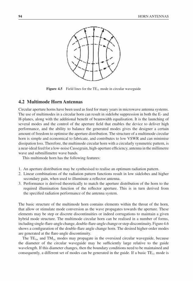
94 HORN ANTENNAS
Figure 4.5 Field lines for the TE11 mode in circular waveguide
4.2 Multimode Horn Antennas
Circular aperture horns have been used as feed for many years in microwave antenna systems.The use of multimodes in a circular horn can result in sidelobe suppression in both the E- andH-planes, along with the additional benefit of beamwidth equalisation. It is the launching ofseveral modes and the control of the aperture field that enables the device to deliver highperformance, and the ability to balance the generated modes gives the designer a certainamount of freedom to optimise the aperture distribution. The structure of a multimode circularhorn is simple and economical to fabricate, and contributes to low VSWR and can minimisedissipation loss. Therefore, the multimode circular horn with a circularly symmetric pattern, isa near-ideal feed for a low-noise Cassegrain, high-aperture efficiency, antenna in the millimetrewave and submillimetre wave bands.
This multimode horn has the following features:
1. An aperture distribution may be synthesised to realise an optimum radiation pattern.2. Linear combinations of the radiation pattern functions result in low sidelobes and higher
secondary gain, when used to illuminate a reflector antenna.3. Performance is derived theoretically to match the aperture distribution of the horn to the
required illumination function of the reflector aperture. This is in turn derived fromthe specified radiation performance of the antenna system.
The basic structure of the multimode horn contains elements within the throat of the horn,that allow or stimulate mode conversion as the wave propagates towards the aperture. Theseelements may be step or discrete discontinuities or indeed corrugations to maintain a givenhybrid mode structure. The multimode circular horn can be realised in a number of forms,including single-flare-angle change, double-flare-angle change or step-discontinuity. Figure 4.6shows a configuration of the double-flare angle change horn. The desired higher-order modesare generated at the flare-angle discontinuity.
The TE1m and TM1n modes may propagate in the oversized circular waveguide, becausethe diameter of the circular waveguide may be sufficiently large relative to the guidewavelength. If this diameter changes, then the boundary conditions need to be maintained andconsequently, a different set of modes can be generated in the guide. If a basic TE11 mode is
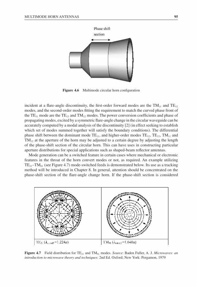
MULTIMODE HORN ANTENNAS 95
Figure 4.6 Multimode circular horn configuration
incident at a flare-angle discontinuity, the first-order forward modes are the TM11 and TE12
modes, and the second-order modes fitting the requirement to match the curved phase front ofthe TE11 mode are the TE13 and TM12 modes. The power conversion coefficients and phase ofpropagating modes, excited by a symmetric flare-angle change in the circular waveguide can beaccurately computed by a modal analysis of the discontinuity [2] (in effect seeking to establishwhich set of modes summed together will satisfy the boundary conditions). The differentialphase shift between the dominant mode TE11, and higher-order modes TE12, TE13, TM11 andTM12 at the aperture of the horn may be adjusted to a certain degree by adjusting the lengthof the phase-shift section of the circular horn. This can have uses in constructing particularaperture distributions for special applications such as shaped-beam reflector antennas.
Mode generation can be a switched feature in certain cases where mechanical or electronicfeatures in the throat of the horn convert modes or not, as required. An example utilizingTE21–TM01 (see Figure 4.7) mode-switched feeds is demonstrated below. Its use as a trackingmethod will be introduced in Chapter 8. In general, attention should be concentrated on thephase-shift section of the flare-angle change horn. If the phase-shift section is considered
Figure 4.7 Field distribution for TE21 and TM01 modes. Source: Baden Fuller, A. J. Microwaves: anintroduction to microwave theory and techniques: 2nd Ed. Oxford; New York: Pergamon, 1979
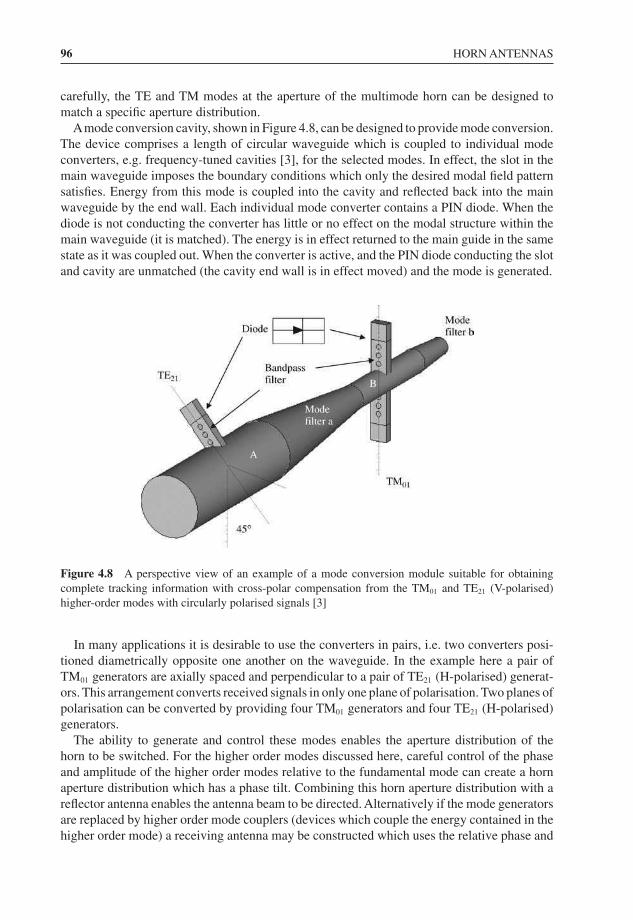
96 HORN ANTENNAS
carefully, the TE and TM modes at the aperture of the multimode horn can be designed tomatch a specific aperture distribution.
Amode conversion cavity, shown in Figure 4.8, can be designed to provide mode conversion.The device comprises a length of circular waveguide which is coupled to individual modeconverters, e.g. frequency-tuned cavities [3], for the selected modes. In effect, the slot in themain waveguide imposes the boundary conditions which only the desired modal field patternsatisfies. Energy from this mode is coupled into the cavity and reflected back into the mainwaveguide by the end wall. Each individual mode converter contains a PIN diode. When thediode is not conducting the converter has little or no effect on the modal structure within themain waveguide (it is matched). The energy is in effect returned to the main guide in the samestate as it was coupled out. When the converter is active, and the PIN diode conducting the slotand cavity are unmatched (the cavity end wall is in effect moved) and the mode is generated.
Figure 4.8 A perspective view of an example of a mode conversion module suitable for obtainingcomplete tracking information with cross-polar compensation from the TM01 and TE21 (V-polarised)higher-order modes with circularly polarised signals [3]
In many applications it is desirable to use the converters in pairs, i.e. two converters posi-tioned diametrically opposite one another on the waveguide. In the example here a pair ofTM01 generators are axially spaced and perpendicular to a pair of TE21 (H-polarised) generat-ors. This arrangement converts received signals in only one plane of polarisation. Two planes ofpolarisation can be converted by providing four TM01 generators and four TE21 (H-polarised)generators.
The ability to generate and control these modes enables the aperture distribution of thehorn to be switched. For the higher order modes discussed here, careful control of the phaseand amplitude of the higher order modes relative to the fundamental mode can create a hornaperture distribution which has a phase tilt. Combining this horn aperture distribution with areflector antenna enables the antenna beam to be directed. Alternatively if the mode generatorsare replaced by higher order mode couplers (devices which couple the energy contained in thehigher order mode) a receiving antenna may be constructed which uses the relative phase and
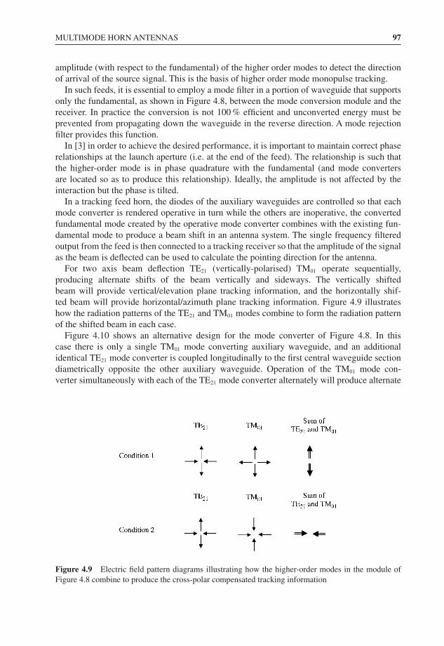
MULTIMODE HORN ANTENNAS 97
amplitude (with respect to the fundamental) of the higher order modes to detect the directionof arrival of the source signal. This is the basis of higher order mode monopulse tracking.
In such feeds, it is essential to employ a mode filter in a portion of waveguide that supportsonly the fundamental, as shown in Figure 4.8, between the mode conversion module and thereceiver. In practice the conversion is not 100 % efficient and unconverted energy must beprevented from propagating down the waveguide in the reverse direction. A mode rejectionfilter provides this function.
In [3] in order to achieve the desired performance, it is important to maintain correct phaserelationships at the launch aperture (i.e. at the end of the feed). The relationship is such thatthe higher-order mode is in phase quadrature with the fundamental (and mode convertersare located so as to produce this relationship). Ideally, the amplitude is not affected by theinteraction but the phase is tilted.
In a tracking feed horn, the diodes of the auxiliary waveguides are controlled so that eachmode converter is rendered operative in turn while the others are inoperative, the convertedfundamental mode created by the operative mode converter combines with the existing fun-damental mode to produce a beam shift in an antenna system. The single frequency filteredoutput from the feed is then connected to a tracking receiver so that the amplitude of the signalas the beam is deflected can be used to calculate the pointing direction for the antenna.
For two axis beam deflection TE21 (vertically-polarised) TM01 operate sequentially,producing alternate shifts of the beam vertically and sideways. The vertically shiftedbeam will provide vertical/elevation plane tracking information, and the horizontally shif-ted beam will provide horizontal/azimuth plane tracking information. Figure 4.9 illustrateshow the radiation patterns of the TE21 and TM01 modes combine to form the radiation patternof the shifted beam in each case.
Figure 4.10 shows an alternative design for the mode converter of Figure 4.8. In thiscase there is only a single TM01 mode converting auxiliary waveguide, and an additionalidentical TE21 mode converter is coupled longitudinally to the first central waveguide sectiondiametrically opposite the other auxiliary waveguide. Operation of the TM01 mode con-verter simultaneously with each of the TE21 mode converter alternately will produce alternate
Figure 4.9 Electric field pattern diagrams illustrating how the higher-order modes in the module ofFigure 4.8 combine to produce the cross-polar compensated tracking information
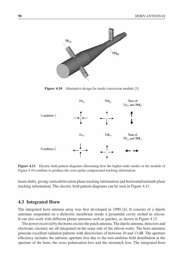
98 HORN ANTENNAS
Figure 4.10 Alternative design for mode conversion module [3]
Figure 4.11 Electric field pattern diagrams illustrating how the higher-order modes in the module ofFigure 4.10 combine to produce the cross-polar compensated tracking information
beam shifts, giving vertical/elevation plane tracking information and horizontal/azimuth planetracking information. The electric field pattern diagrams can be seen in Figure 4.11.
4.3 Integrated Horn
The integrated horn antenna array was first developed in 1990 [4]. It consists of a dipoleantennas suspended on a dielectric membrane inside a pyramidal cavity etched in silicon.It can also work with different planar antennas such as patches, as shown in Figure 4.12.
The power received by the horns excites the patch antenna. The dipole antenna, detectors andelectronic circuitry are all integrated on the same side of the silicon wafer. The horn antennasgenerate excellent radiation patterns with directivities of between 10 and 13 dB. The apertureefficiency includes the intrinsic aperture loss due to the non-uniform field distribution at theaperture of the horn, the cross polarisation loss and the mismatch loss. The integrated horn
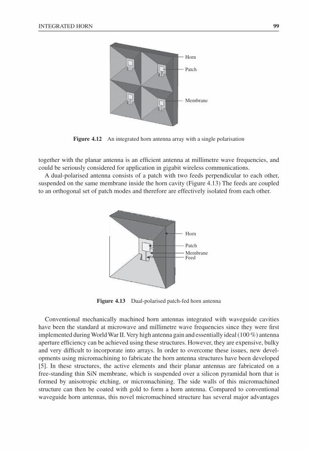
INTEGRATED HORN 99
Horn
Patch
Membrane
Figure 4.12 An integrated horn antenna array with a single polarisation
together with the planar antenna is an efficient antenna at millimetre wave frequencies, andcould be seriously considered for application in gigabit wireless communications.
A dual-polarised antenna consists of a patch with two feeds perpendicular to each other,suspended on the same membrane inside the horn cavity (Figure 4.13) The feeds are coupledto an orthogonal set of patch modes and therefore are effectively isolated from each other.
Horn
Patch
MembraneFeed
Figure 4.13 Dual-polarised patch-fed horn antenna
Conventional mechanically machined horn antennas integrated with waveguide cavitieshave been the standard at microwave and millimetre wave frequencies since they were firstimplemented during World War II. Very high antenna gain and essentially ideal (100 %) antennaaperture efficiency can be achieved using these structures. However, they are expensive, bulkyand very difficult to incorporate into arrays. In order to overcome these issues, new devel-opments using micromachining to fabricate the horn antenna structures have been developed[5]. In these structures, the active elements and their planar antennas are fabricated on afree-standing thin SiN membrane, which is suspended over a silicon pyramidal horn that isformed by anisotropic etching, or micromachining. The side walls of this micromachinedstructure can then be coated with gold to form a horn antenna. Compared to conventionalwaveguide horn antennas, this novel micromachined structure has several major advantages
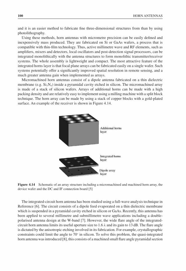
100 HORN ANTENNAS
and it is an easier method to fabricate fine three-dimensional structures from than by usingphotolithography.
Using these methods, horn antennas with micrometre precision can be easily defined andinexpensively mass produced. They are fabricated on Si or GaAs wafers, a process that iscompatible with thin-film technology. Thus, active millimetre wave and RF elements, such asamplifiers, mixers and detectors, local oscillators and post-detection signal processors, can beintegrated monolithically with the antenna structures to form monolithic transmitter/receiversystems. The whole assembly is lightweight and compact. The most attractive feature of theintegrated horns layer is that focal plane arrays can be fabricated easily on a single wafer. Suchsystems potentially offer a significantly improved spatial resolution in remote sensing, and amuch greater antenna gain when implemented as arrays.
Micromachined horn antennas consist of a dipole antenna fabricated on a thin dielectricmembrane (e.g. Si3N4) inside a pyramidal cavity etched in silicon. The micromachined arrayis made of a stack of silicon wafers. Arrays of additional horns can be made with a highpacking density and are relatively easy to implement using a milling machine with a split blocktechnique. The horn array can be made by using a stack of copper blocks with a gold-platedsurface. An example of the receiver is shown in Figure 4.14.
Figure 4.14 Schematic of an array structure including a micromachined and machined horn array, thedevice wafer and the DC and IF connection board [5]
The integrated-circuit horn antenna has been studied using a full-wave analysis technique inReference [6]. The circuit consists of a dipole feed evaporated on a thin dielectric membranewhich is suspended in a pyramidal cavity etched in silicon or GaAs. Recently, this antenna hasbeen applied to several millimetre and submillimetre wave applications including a double-polarised antenna design at the W-band [7]. However, the wide flare angle of the integrated-circuit horn antenna limits its useful aperture size to 1.6 λ and its gain to 13 dB. The flare angleis dictated by the anisotropic etching involved in its fabrication. For example, crystallographicconstraints could limit the angle to 70◦ in silicon. To solve this problem, the quasi-integratedhorn antenna was introduced [8], this consists of a machined small flare angle pyramidal section
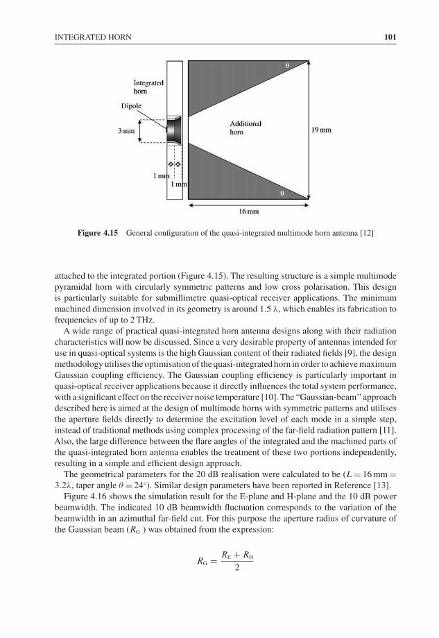
INTEGRATED HORN 101
Figure 4.15 General configuration of the quasi-integrated multimode horn antenna [12]
attached to the integrated portion (Figure 4.15). The resulting structure is a simple multimodepyramidal horn with circularly symmetric patterns and low cross polarisation. This designis particularly suitable for submillimetre quasi-optical receiver applications. The minimummachined dimension involved in its geometry is around 1.5 λ, which enables its fabrication tofrequencies of up to 2 THz.
A wide range of practical quasi-integrated horn antenna designs along with their radiationcharacteristics will now be discussed. Since a very desirable property of antennas intended foruse in quasi-optical systems is the high Gaussian content of their radiated fields [9], the designmethodology utilises the optimisation of the quasi-integrated horn in order to achieve maximumGaussian coupling efficiency. The Gaussian coupling efficiency is particularly important inquasi-optical receiver applications because it directly influences the total system performance,with a significant effect on the receiver noise temperature [10]. The “Gaussian-beam’’approachdescribed here is aimed at the design of multimode horns with symmetric patterns and utilisesthe aperture fields directly to determine the excitation level of each mode in a simple step,instead of traditional methods using complex processing of the far-field radiation pattern [11].Also, the large difference between the flare angles of the integrated and the machined parts ofthe quasi-integrated horn antenna enables the treatment of these two portions independently,resulting in a simple and efficient design approach.
The geometrical parameters for the 20 dB realisation were calculated to be (L= 16 mm =3.2λ, taper angle θ = 24◦). Similar design parameters have been reported in Reference [13].
Figure 4.16 shows the simulation result for the E-plane and H-plane and the 10 dB powerbeamwidth. The indicated 10 dB beamwidth fluctuation corresponds to the variation of thebeamwidth in an azimuthal far-field cut. For this purpose the aperture radius of curvature ofthe Gaussian beam (RG ) was obtained from the expression:
RG = RE + RH
2
102 HORN ANTENNAS
Figure 4.16 The E- (–�–) and H-plane (–�–) patterns of the 20 dB quasi-integrated horn
where RE and RH are the radii of curvature of the aperture field in the E-plane and H-planecuts respectively, and were obtained from a least-squares fit to the phase of the aperture field.Also, the Gaussian-beam roll-off was calculated at the edges of the ±5 % bandwidth using theGaussian-beam parameters, which were calculated at the design frequency f0.
4.4 Conical Horns and Circular Polarisation
Figure 4.17 shows an array antenna consisting of 2 × 2 patch array antennas with multiplemicrostrip feeding lines, four circular horns and four phase shifters [14]. Four square patcheswith truncated corners are included to generate right-hand circular polarisation (this is a simplemethod of generating circular polarisation which avoids two orthogonal feeder lines). The rel-ative orientation of each patch is 90◦ rotated clockwise around the centre point of the array[15]. Thus, the feed to each patch has a 90◦ angular orientation, as shown in Figure 4.17. Withthis spacing, the fields generated from the four feeds are orthogonal to each other. Addition-ally, the four feeds are required to be fed 90◦ out-of-phase to achieve TM11 mode circularpolarisation. The phase of each patch is therefore 0◦, 90◦, 180◦ and 270◦, respectively, in aclockwise direction [15]. For left-hand circular polarisation (LHCP), the electric field vectorwill rotate in the opposite direction. The phase settings for both RHCP and LHCP are illustratedin Table 4.2.
The phase difference of 90◦ can be produced by either adjusting the length of the microstripfeeding lines or using a branch-line coupler. As a result, the radiation summation of the 2 × 2array is right-hand circular polarisation. The prototypes of feeding lines and patch antennasare printed using a gold layer on a ceramic substrate (εr = 10). The size of a 61 GHz patch is0.72 mm by 0.72 mm approximately.
The integrated conical horn array is placed in the ground plane to improve the gain andbandwidth of the patches, and the centre of the patch is aligned with the axis of the horn.A patch and its surrounding horn are considered together to be one radiation element. The
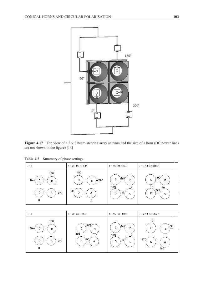
CONICAL HORNS AND CIRCULAR POLARISATION 103
Figure 4.17 Top view of a 2 × 2 beam-steering array antenna and the size of a horn (DC power linesare not shown in the figure) [14]
Table 4.2 Summary of phase settings
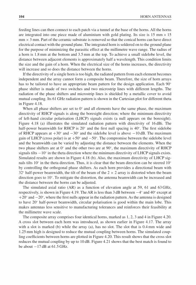
104 HORN ANTENNAS
feeding lines can then connect to each patch via a tunnel at the base of the horns. All the hornsare integrated into one piece made of aluminium with gold plating. Its size is 15 mm × 15mm × 3 mm. Part of the ceramic substrate is removed so that the conical horns can have directelectrical contact with the ground plane. The integrated horn is soldered on to the ground planefor the purpose of minimizing the parasitic effect at the millimetre wave range. The radius ofa horn is 1.8 mm at the bottom and 3.5 mm at the top. To achieve a small sidelobe level, thedistance between adjacent elements is approximately half a wavelength. This condition limitsthe size and the gain of a horn. When the electrical size of the horns increases, the directivitywill increase and so does the distance between the horns.
If the directivity of a single horn is too high, the radiated pattern from each element becomesindependent and the array cannot form a composite beam. Therefore, the size of horn arrayshas to be tailored to have an appropriate beam pattern for the design application. Each 90◦
phase shifter is made of two switches and two microstrip lines with different lengths. Theradiation of the phase shifters and microstrip lines is shielded by a metallic cover to avoidmutual coupling. Its 61 GHz radiation pattern is shown in the Cartesian plot for different thetain Figure 4.18.
When all phase shifters are set to 0◦ and all elements have the same phase, the maximumdirectivity of RHCP signals is along the boresight direction; where the minimum directivityof left-hand circular polarisation (LHCP) signals exists (a null appears on the boresight).Figure 4.18 (a) illustrates the simulated radiation pattern with directivity of 16 dBi. Thehalf-power beamwidth for RHCP is 20◦ and the first null spacing is 40◦. The first sidelobeof RHCP appears at +30◦ and −30◦ and the sidelobe level is above −10 dB. The maximumgain of LHCP (cross polar) is at +50◦ and −50◦. The compromise between the sidelobe leveland the beamwidth can be varied by adjusting the distance between the elements. When thetwo phase shifters are at 0◦ and the other two are at 90◦, the maximum directivity of RHCPsignals tilts −10◦ in the theta direction where the minimum directivity of LHCP signals exists.Simulated results are shown in Figure 4.18 (b). Also, the maximum directivity of LHCP sig-nals tilts 10◦ in the theta direction. Thus, it is clear that the beam direction can be steered 10◦
by controlling the orthogonal phase shifters. As each horn provides a directional beam with32◦ half-power beamwidth, the tilt of the beam of the 2 × 2 array is distorted when the beamdirection goes to 10◦. To mitigate the distortion, the antenna beamwidth can be increased andthe distance between the horns can be adjusted.
The simulated axial ratio (AR) as a function of elevation angle at 59, 61 and 63 GHz,respectively, is shown in Figure 4.19. The AR is less than 3 dB between −4◦ and 40◦ except at+20◦ and −20◦, where the first nulls appear in the radiation pattern. As the antenna is designedto have 20◦ half-power beamwidth, circular polarisation is good within the main lobe. Thismakes antennas less sensitive to manufacturing tolerances and reinforces their feasibility atthe millimetre wave scale.
The composite array comprises four identical horns, marked as 1, 2, 3 and 4 in Figure 4.20.A cross slot between each horn was introduced, as shown earlier in Figure 4.17. The arraywith a slot is marked (b) while the array (a), has no slot. The slot that is 0.4 mm wide and1.25 mm high is designed to reduce the mutual coupling between horns. The simulated coup-ling coefficients between horns are plotted in Figure 4.20. This result shows that the cross slotreduces the mutual coupling by up to 10 dB. Figure 4.21 shows that the best match is found tobe about −17 dB at 61.5 GHz.
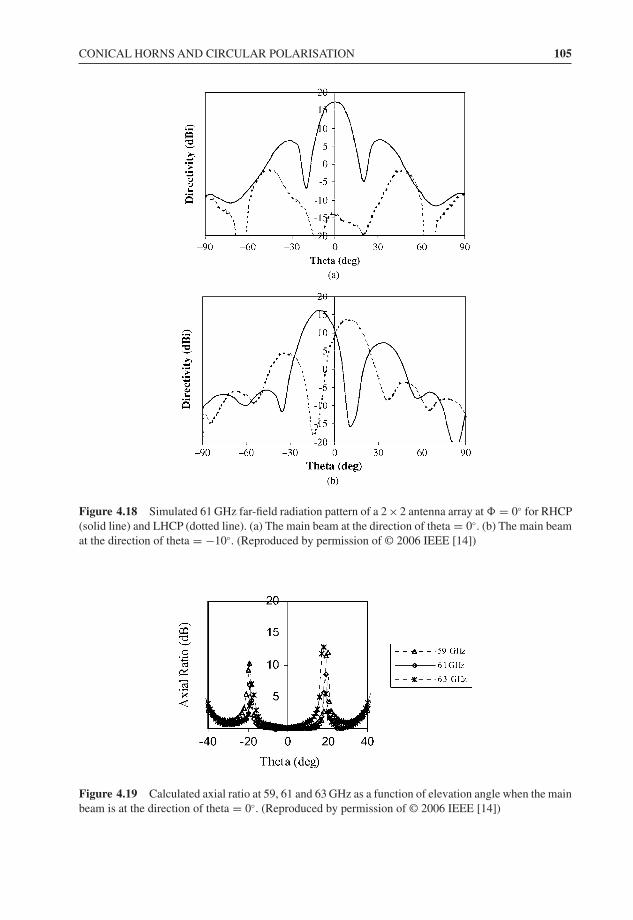
CONICAL HORNS AND CIRCULAR POLARISATION 105
Figure 4.18 Simulated 61 GHz far-field radiation pattern of a 2 × 2 antenna array at = 0◦ for RHCP(solid line) and LHCP (dotted line). (a) The main beam at the direction of theta = 0◦. (b) The main beamat the direction of theta = −10◦. (Reproduced by permission of © 2006 IEEE [14])
Figure 4.19 Calculated axial ratio at 59, 61 and 63 GHz as a function of elevation angle when the mainbeam is at the direction of theta = 0◦. (Reproduced by permission of © 2006 IEEE [14])
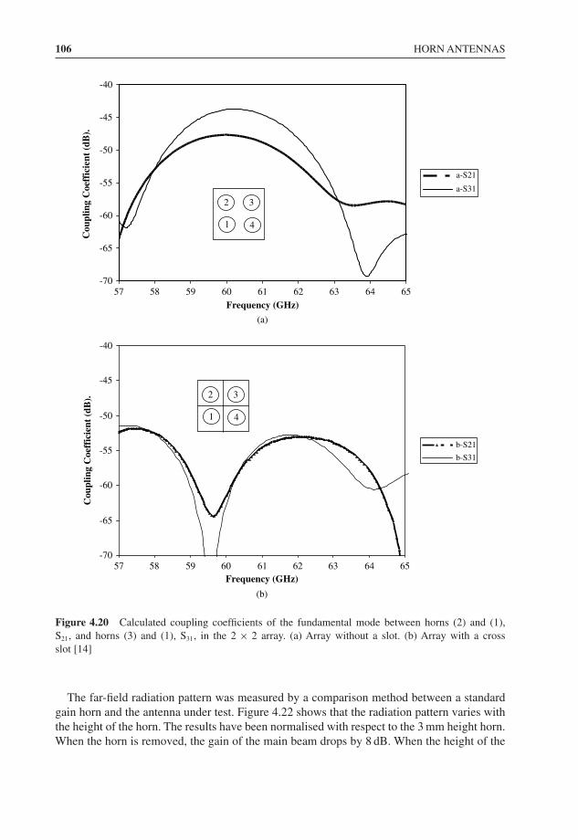
106 HORN ANTENNAS
-70
-65
-60
-55
-50
-45
-40
57 58 59 60 61 62 63 64 65Frequency (GHz)
Cou
plin
g C
oeff
icie
nt (
dB).
a-S21
a-S31
(a)
1
2 3
4
b-S21
b-S31
1
2 3
4
-70
-65
-60
-55
-50
-45
-40
57 58 59 60 61 62 63 64 65Frequency (GHz)
Cou
plin
g C
oeff
icie
nt (
dB).
(b)
Figure 4.20 Calculated coupling coefficients of the fundamental mode between horns (2) and (1),S21, and horns (3) and (1), S31, in the 2 × 2 array. (a) Array without a slot. (b) Array with a crossslot [14]
The far-field radiation pattern was measured by a comparison method between a standardgain horn and the antenna under test. Figure 4.22 shows that the radiation pattern varies withthe height of the horn. The results have been normalised with respect to the 3 mm height horn.When the horn is removed, the gain of the main beam drops by 8 dB. When the height of the
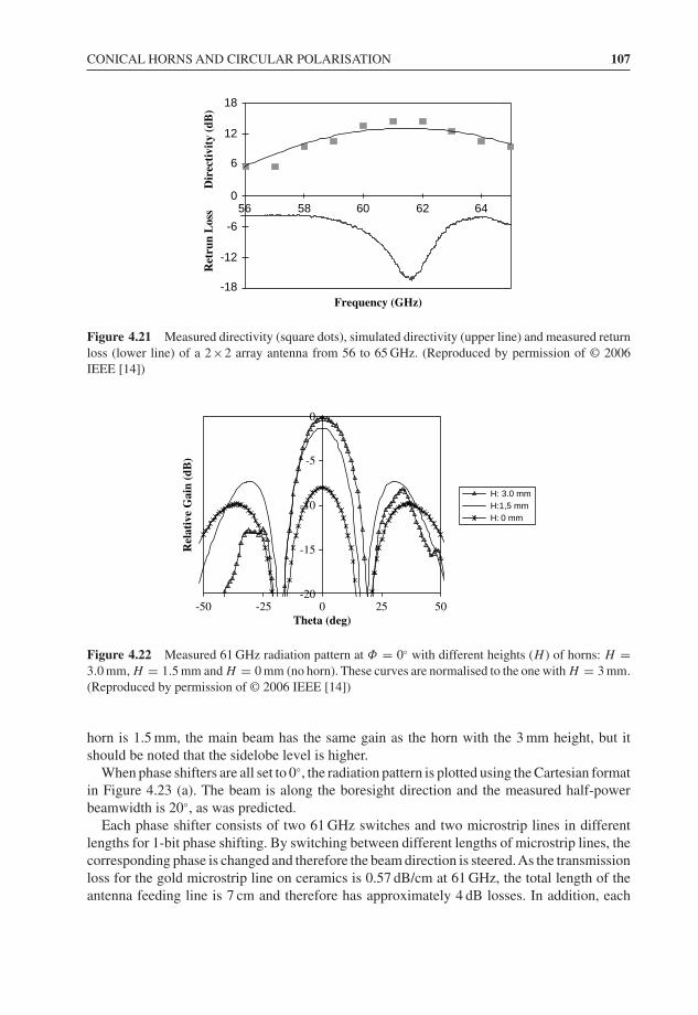
CONICAL HORNS AND CIRCULAR POLARISATION 107
-18
-12
-6
0
6
12
18
56 58 60 62 64
Frequency (GHz)
Dir
ecti
vity
(dB
)R
etru
n L
oss
Figure 4.21 Measured directivity (square dots), simulated directivity (upper line) and measured returnloss (lower line) of a 2×2 array antenna from 56 to 65 GHz. (Reproduced by permission of © 2006IEEE [14])
-20
-15
-10
-5
0
-50 -25 0 25 50Theta (deg)
Rel
ativ
e G
ain
(dB
)
H: 3.0 mmH:1,5 mmH: 0 mm
Figure 4.22 Measured 61 GHz radiation pattern at Φ = 0◦ with different heights (H ) of horns: H =3.0 mm, H = 1.5 mm and H = 0 mm (no horn). These curves are normalised to the one with H = 3 mm.(Reproduced by permission of © 2006 IEEE [14])
horn is 1.5 mm, the main beam has the same gain as the horn with the 3 mm height, but itshould be noted that the sidelobe level is higher.
When phase shifters are all set to 0◦, the radiation pattern is plotted using the Cartesian formatin Figure 4.23 (a). The beam is along the boresight direction and the measured half-powerbeamwidth is 20◦, as was predicted.
Each phase shifter consists of two 61 GHz switches and two microstrip lines in differentlengths for 1-bit phase shifting. By switching between different lengths of microstrip lines, thecorresponding phase is changed and therefore the beam direction is steered.As the transmissionloss for the gold microstrip line on ceramics is 0.57 dB/cm at 61 GHz, the total length of theantenna feeding line is 7 cm and therefore has approximately 4 dB losses. In addition, each
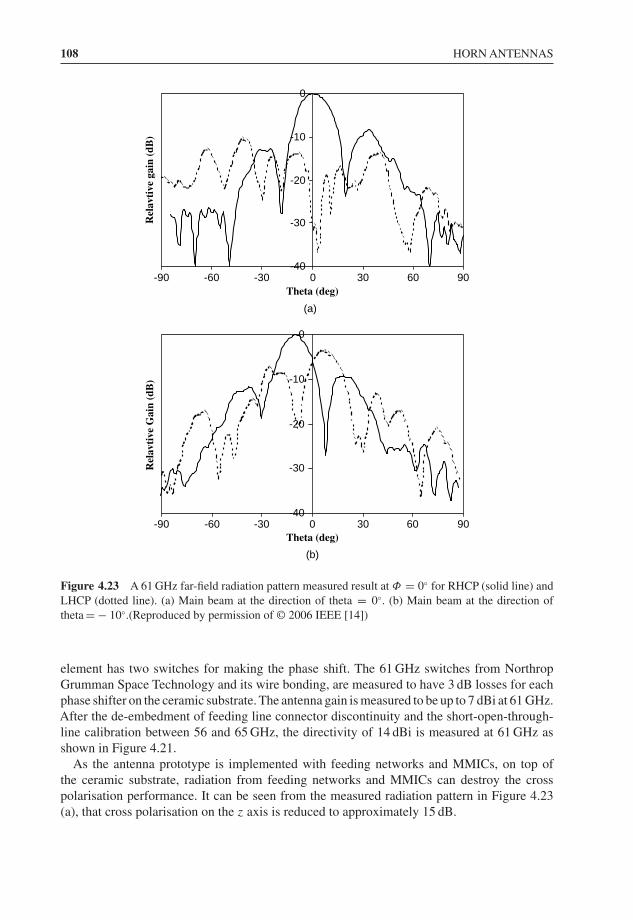
108 HORN ANTENNAS
-40
-30
-20
-10
0
Theta (deg)
Rel
avti
ve g
ain
(dB
)R
elav
tive
Gai
n (d
B)
(a)
-40
-30
-20
-10
0
-90 -60 -30 0 30 60 90
-90 -60 -30 0 30 60 90Theta (deg)
(b)
Figure 4.23 A 61 GHz far-field radiation pattern measured result at Φ = 0◦ for RHCP (solid line) andLHCP (dotted line). (a) Main beam at the direction of theta = 0◦. (b) Main beam at the direction oftheta = − 10◦.(Reproduced by permission of © 2006 IEEE [14])
element has two switches for making the phase shift. The 61 GHz switches from NorthropGrumman Space Technology and its wire bonding, are measured to have 3 dB losses for eachphase shifter on the ceramic substrate. The antenna gain is measured to be up to 7 dBi at 61 GHz.After the de-embedment of feeding line connector discontinuity and the short-open-through-line calibration between 56 and 65 GHz, the directivity of 14 dBi is measured at 61 GHz asshown in Figure 4.21.
As the antenna prototype is implemented with feeding networks and MMICs, on top ofthe ceramic substrate, radiation from feeding networks and MMICs can destroy the crosspolarisation performance. It can be seen from the measured radiation pattern in Figure 4.23(a), that cross polarisation on the z axis is reduced to approximately 15 dB.
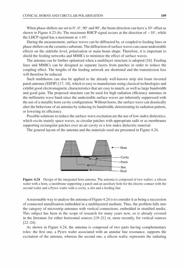
CONICAL HORNS AND CIRCULAR POLARISATION 109
When phase shifters are set to 0◦, 0◦, 90◦ and 90◦, the beam direction can have a 10◦ offset asshown in Figure 4.23 (b). The maximum RHCP signal occurs at the direction of −10◦, whilethe LHCP signal has a maximum at +10◦.
During the measurement, surface waves can be diffracted by, or coupled to feeding lines orphase shifters on the ceramics substrate. The diffraction of surface waves can cause undesirableeffects on the sidelobe level, polarisation or main beam shape. Therefore, it is important toshield the feeding networks and MMICs to minimize the effect of surface waves.
The antenna can be further optimised when a multilayer structure is adopted [16]. Feedinglines and MMICs can be designed as separate layers from patches in order to reduce thecoupling effect. The lengths of the feeding network are shortened and the transmission losswill therefore be reduced.
Such multihorns can also be applied to the already well-known strip slot foam invertedpatch antenna (SSFIP) [17, 18], which is easy to manufacture using classical technologies andexhibit good electromagnetic characteristics that are easy to match, as well as large bandwidthand good gain. The proposed structure can be used for high radiation efficiency antennas inthe millimetre wave band since the undesirable surface waves are inherently suppressed withthe use of a metallic horn cavity configuration. Without horns, the surface wave can drasticallyalter the behaviour of an antenna by reducing its bandwidth, deteriorating its radiation pattern,or lowering its efficiency.
Possible solutions to reduce the surface-wave excitation are the use of low-index dielectrics,which excite mainly space waves, as circular patches with appropriate radii or as membranessupporting rectangular patches over an air cavity or a low-index dielectric material.
The general layout of the antenna and the materials used are presented in Figure 4.24.
Figure 4.24 Design of the integrated horn antenna. The antenna is composed of two wafers: a siliconwafer with a horn, a membrane supporting a patch and an auxiliary hole for the electric contact with thesecond wafer and a Pyrex wafer with a cavity, a slot and a feeding line
A reasonable way to analyse the antenna of Figure 4.24 is to consider it as being a successionof connected metallisation embedded in a multilayered medium. Thus, the problem falls intothe category of microstrip antennas with vertical connections, embedded in stratified media.This subject has been in the scope of research for many years now, so is already coveredin the literature for either horizontal sources [19–21] or, more recently, for vertical sources[22–24].
As shown in Figure 4.24, the antenna is composed of two parts having complementaryroles: the first one, a Pyrex wafer associated with an annular line resonance, supports theexcitation of the antenna, whereas the second one, a silicon wafer, represents the radiating
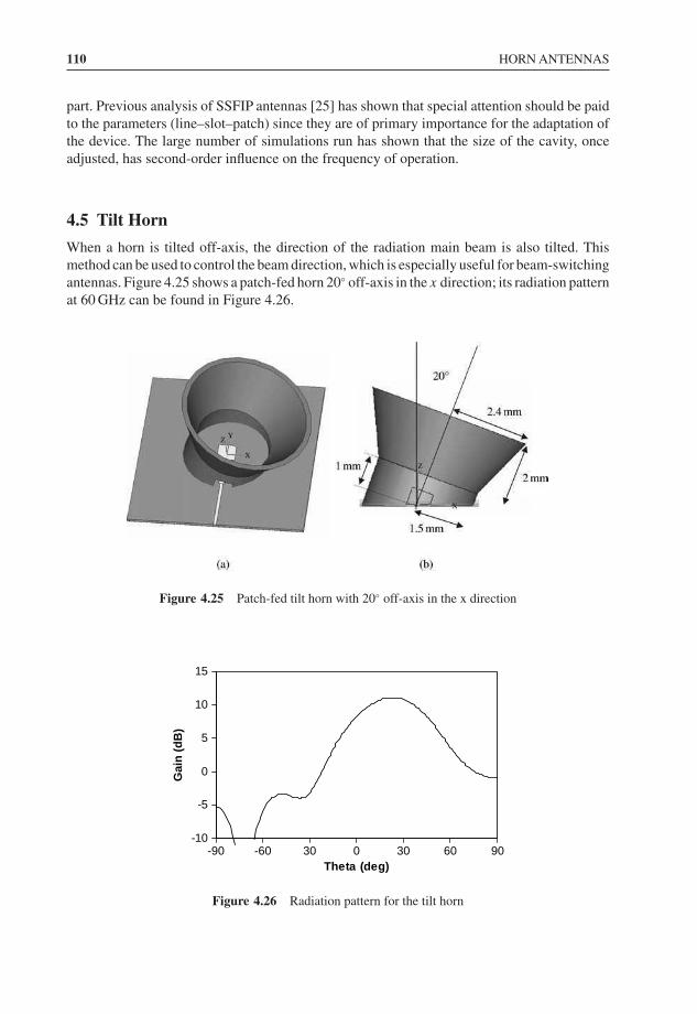
110 HORN ANTENNAS
part. Previous analysis of SSFIP antennas [25] has shown that special attention should be paidto the parameters (line–slot–patch) since they are of primary importance for the adaptation ofthe device. The large number of simulations run has shown that the size of the cavity, onceadjusted, has second-order influence on the frequency of operation.
4.5 Tilt Horn
When a horn is tilted off-axis, the direction of the radiation main beam is also tilted. Thismethod can be used to control the beam direction, which is especially useful for beam-switchingantennas. Figure 4.25 shows a patch-fed horn 20◦ off-axis in the x direction; its radiation patternat 60 GHz can be found in Figure 4.26.
Figure 4.25 Patch-fed tilt horn with 20◦ off-axis in the x direction
-10
-5
0
5
10
15
-90 -60 30 0 30 60 90Theta (deg)
Gai
n (
dB
)
Figure 4.26 Radiation pattern for the tilt horn
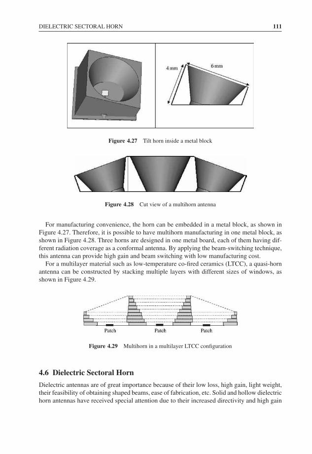
DIELECTRIC SECTORAL HORN 111
Figure 4.27 Tilt horn inside a metal block
Figure 4.28 Cut view of a multihorn antenna
For manufacturing convenience, the horn can be embedded in a metal block, as shown inFigure 4.27. Therefore, it is possible to have multihorn manufacturing in one metal block, asshown in Figure 4.28. Three horns are designed in one metal board, each of them having dif-ferent radiation coverage as a conformal antenna. By applying the beam-switching technique,this antenna can provide high gain and beam switching with low manufacturing cost.
For a multilayer material such as low-temperature co-fired ceramics (LTCC), a quasi-hornantenna can be constructed by stacking multiple layers with different sizes of windows, asshown in Figure 4.29.
Figure 4.29 Multihorn in a multilayer LTCC configuration
4.6 Dielectric Sectoral Horn
Dielectric antennas are of great importance because of their low loss, high gain, light weight,their feasibility of obtaining shaped beams, ease of fabrication, etc. Solid and hollow dielectrichorn antennas have received special attention due to their increased directivity and high gain
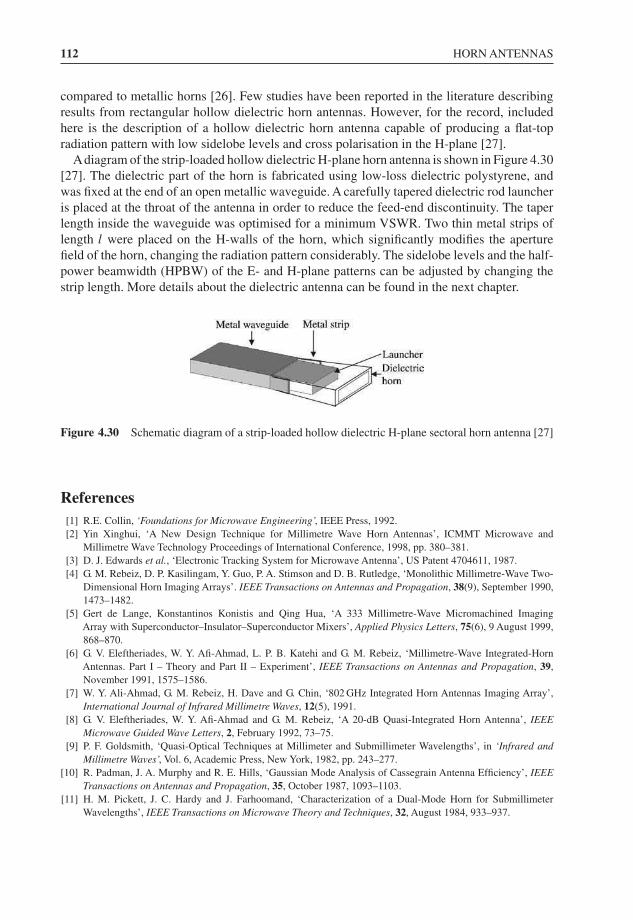
112 HORN ANTENNAS
compared to metallic horns [26]. Few studies have been reported in the literature describingresults from rectangular hollow dielectric horn antennas. However, for the record, includedhere is the description of a hollow dielectric horn antenna capable of producing a flat-topradiation pattern with low sidelobe levels and cross polarisation in the H-plane [27].
Adiagram of the strip-loaded hollow dielectric H-plane horn antenna is shown in Figure 4.30[27]. The dielectric part of the horn is fabricated using low-loss dielectric polystyrene, andwas fixed at the end of an open metallic waveguide. A carefully tapered dielectric rod launcheris placed at the throat of the antenna in order to reduce the feed-end discontinuity. The taperlength inside the waveguide was optimised for a minimum VSWR. Two thin metal strips oflength l were placed on the H-walls of the horn, which significantly modifies the aperturefield of the horn, changing the radiation pattern considerably. The sidelobe levels and the half-power beamwidth (HPBW) of the E- and H-plane patterns can be adjusted by changing thestrip length. More details about the dielectric antenna can be found in the next chapter.
Figure 4.30 Schematic diagram of a strip-loaded hollow dielectric H-plane sectoral horn antenna [27]
References[1] R.E. Collin, ‘Foundations for Microwave Engineering’, IEEE Press, 1992.[2] Yin Xinghui, ‘A New Design Technique for Millimetre Wave Horn Antennas’, ICMMT Microwave and
Millimetre Wave Technology Proceedings of International Conference, 1998, pp. 380–381.[3] D. J. Edwards et al., ‘Electronic Tracking System for Microwave Antenna’, US Patent 4704611, 1987.[4] G. M. Rebeiz, D. P. Kasilingam, Y. Guo, P. A. Stimson and D. B. Rutledge, ‘Monolithic Millimetre-Wave Two-
Dimensional Horn Imaging Arrays’. IEEE Transactions on Antennas and Propagation, 38(9), September 1990,1473–1482.
[5] Gert de Lange, Konstantinos Konistis and Qing Hua, ‘A 333 Millimetre-Wave Micromachined ImagingArray with Superconductor–Insulator–Superconductor Mixers’, Applied Physics Letters, 75(6), 9 August 1999,868–870.
[6] G. V. Eleftheriades, W. Y. Afi-Ahmad, L. P. B. Katehi and G. M. Rebeiz, ‘Millimetre-Wave Integrated-HornAntennas. Part I – Theory and Part II – Experiment’, IEEE Transactions on Antennas and Propagation, 39,November 1991, 1575–1586.
[7] W. Y. Ali-Ahmad, G. M. Rebeiz, H. Dave and G. Chin, ‘802 GHz Integrated Horn Antennas Imaging Array’,International Journal of Infrared Millimetre Waves, 12(5), 1991.
[8] G. V. Eleftheriades, W. Y. Afi-Ahmad and G. M. Rebeiz, ‘A 20-dB Quasi-Integrated Horn Antenna’, IEEEMicrowave Guided Wave Letters, 2, February 1992, 73–75.
[9] P. F. Goldsmith, ‘Quasi-Optical Techniques at Millimeter and Submillimeter Wavelengths’, in ‘Infrared andMillimetre Waves’, Vol. 6, Academic Press, New York, 1982, pp. 243–277.
[10] R. Padman, J. A. Murphy and R. E. Hills, ‘Gaussian Mode Analysis of Cassegrain Antenna Efficiency’, IEEETransactions on Antennas and Propagation, 35, October 1987, 1093–1103.
[11] H. M. Pickett, J. C. Hardy and J. Farhoomand, ‘Characterization of a Dual-Mode Horn for SubmillimeterWavelengths’, IEEE Transactions on Microwave Theory and Techniques, 32, August 1984, 933–937.

REFERENCES 113
[12] George V. Eleftheriades and Gabriel M. Rebeiz, ‘Design and Analysis of Quasi-Integrated Horn Antennas forMillimeter and Submillimeter-Wave Applications’, IEEE Transactions on Microwave Theory and Techniques,41(6/7), June/July 1993, 954–965.
[13] P. D. Potter, ‘A New Horn Antenna with Suppressed Sidelobes and Equal Beamwidths’, Microwave Journal, VI,June 1963, 71–78.
[14] K. Huang and Z. Wang, ‘Millimetre-Wave Circular Polarized Beam-Steering Antenna Array for Gigabit WirelessCommunications’, IEEE Transactions on Antennas and Propagation, 54(2), February 2006, 743–746.
[15] K. Huang, S. Koch and M. Uno, ‘Circular Polarized Array Antenna’, European Patent EP1564843.[16] R. Kulke, C. Günner, S. Holzwarth, J. Kassner, A. Lauer, M. Rittweger, P. Uhlig and P. Weigand, ‘24 GHz Radar
Sensor Integrates Patch Antenna and Frontend Module in Single Multilayer LTCC Substrate’, 15th EuropeanMicroelectronics and Packaging Conference (IMAPS), Brugge, 12–15 June 2005, pp. 239–242.
[17] J.-F. Zucher and F .E. Gardiol, ‘SSFIP: A Global Concept for High Performance Broadband Planar Antennas,Electronics Letters, 24, 1988, 1433–1435.
[18] J.-F. Zurcher and F. E. Gardiol, ‘Broadband Patch Antennas’, Artech House, Norwood, Massachusetts, 1995.[19] J. R. Mosig and F. Gardiol, ‘General Integral Equation Formulation for Microstrip Antennas and Scatterers’,
Proceedings of the Institution of Electrical Engineers, 132, 1985, 424–432.[20] J. R. Mosig, ‘Arbitrarily Shaped Microstrip Structures and Their Analysis with a Mixed Potential Integral
Equation’, IEEE Transactions on Microwave Theory and Techniques, 36,1988, 314–323.[21] Y. L. Chow, N. Hojjat, S. Safavi-Naeini and R. Faraji-Dana, ‘Spectral Green’s Functions for Multilayer Media
in a Convenient Computational Form’, Proceedings of the Institution of Electrical Engineers, 145, 1998, 85–91.[22] N. Kinayman and M. I. Aksun, ‘Efficient Use of Closed-Form Green’s Functions for the Analysis of Planar
Geometries with Vertical Connections’, IEEE Transactions on Microwave Theory and Techniques, 45, 1997,593–603.
[23] T. M. Grzegorczyk and J. R. Mosig, ‘Full-Wave Analysis of Antennas Containing Horizontal and VerticalMetalizations Embedded in Multilayered Media’, IEEE Transactions on Antennas and Propagation, 51, 2003,3047–3054.
[24] R. F. Harrington, ‘Field Computation by Moment Method’, IEEE Press, New York, 1993.[25] Y. Brand, ‘Antennes Imprimees SSFIP: de l’Element Isole au Reseau Planaire’, PhD Dissertation, Ecole
Polytechnique Federale ’de Lausanne, Switzerland, 1996.[26] V. P. Joseph, S. Mathew, J. Jacob, U. Ravindranath and K. T. Mathew, ‘Radiation Characteristics of Strip Loaded
Hollow Dielectric Ž. E-Plane Sectoral Horn Antennas’, Electronics Letters, 33, 1997, 2002–2004.[27] V. P. Joseph, S. Biju Kumar and K. T. Mathew, ‘Strip-Loaded Hollow Dielectric H-Plane Sectoral Horn Antennas
for Square Radiation Pattern’, Microwave Optical Technology Letters, 29, 2001, 45–46.

5Dielectric Antennas
Dielectric rod antennas have been used extensively as an endfire radiator for many years, anda considerable number of theoretical and experimental studies for this type of antenna havebeen published at microwave and millimetre wave frequencies [1]. This type of antenna hasthe attractive features of light weight and low cost. Therefore presented here are the basicdesign considerations, properties and feeding techniques. The chapter is divided into sevensections. Section 5.1 introduces the dielectric resonator antenna. Section 5.2 describes thedielectric rod antenna. Section 5.3 continues with maximum gain antennas, and then dual rodsare discussed in Section 5.4. Section 5.5 presents the basic features of a microstrip patch-feddielectric antenna, while Section 5.6 discusses a compensation method for a dielectric arraywith different phase delays to the elements. Finally, Section 5.7 describes techniques for theoptimisation of the performance of a rod antenna.
5.1 Dielectric Resonator Antennas
Dielectric resonators appeared in the 1970s in work that led to the miniaturization of active andpassive microwave components, such as oscillators and filters [2]. In a shielded environment,the resonators built with dielectric resonators can reach an unloaded Q factor of 20 000 atfrequencies of 20 GHz.
The principle of operation of the dielectric resonator can best be understood by studying thepropagation of electromagnetic waves on a dielectric rod waveguide (Reference [2], Chapter 3).The mathematical description [3] and the experimental verification [4] of the existence of thesewaves have been known for a considerable time. Their wide application was prompted by theintroduction of optical fibres in communications systems.
One of the attractive features of a dielectric resonator antenna (DRA) is that it can assume anyone of a number of simple shapes, the most common being ones with circular or rectangularcross-sections, as shown in Figure 5.1. Over the years the frequency range of interest formany systems has gradually progressed upwards to the millimetre and near-millimetre range(100–300 GHz). At these frequencies, the conductor loss of metallic antennas becomes severeand the efficiency of such antennas is significantly reduced. Conversely, the only loss for adielectric resonator antenna is that due to the imperfect dielectric material (the loss tangent
Millimetre Wave Antennas for Gigabit Wireless Communications Kao-Cheng Huang and David J. Edwardsc© 2008 John Wiley & Sons, Ltd
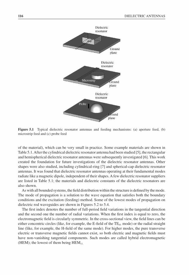
116 DIELECTRIC ANTENNAS
Figure 5.1 Typical dielectric resonator antennas and feeding mechanisms: (a) aperture feed, (b)microstrip feed and (c) probe feed
of the material), which can be very small in practice. Some example materials are shown inTable 5.1.After the cylindrical dielectric resonator antenna had been studied [5], the rectangularand hemispherical dielectric resonator antennas were subsequently investigated [6]. This workcreated the foundation for future investigations of the dielectric resonator antennas. Othershapes were also studied, including cylindrical-ring [7] and spherical-cap dielectric resonatorantennas. It was found that dielectric resonator antennas operating at their fundamental modesradiate like a magnetic dipole, independent of their shapes. A few dielectric resonator suppliersare listed in Table 5.1; the materials and dielectric constants of the dielectric resonators arealso shown.
As with all bounded systems, the field distribution within the structure is defined by the mode.The mode of propagation is a solution to the wave equation that satisfies both the boundaryconditions and the excitation (feeding) method. Some of the lowest modes of propagation ondielectric rod waveguides are shown in Figures 5.2 to 5.4.
The first index denotes the number of full-period field variations in the tangential directionand the second one the number of radial variations. When the first index is equal to zero, theelectromagnetic field is circularly symmetric. In the cross-sectional view, the field lines can beeither concentric circles (like, for example, the E-field of the TE01 mode) or the radial straightline (like, for example, the H-field of the same mode). For higher modes, the pure transverseelectric or transverse magnetic fields cannot exist, so both electric and magnetic fields musthave non-vanishing tangential components. Such modes are called hybrid electromagnetic(HEM); the lowest of them being HEM11.
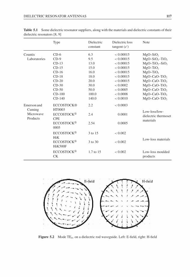
DIELECTRIC RESONATOR ANTENNAS 117
Table 5.1 Some dielectric resonator suppliers, along with the materials and dielectric constants of theirdielectric resonators [8, 9]
Type Dielectricconstant
Dielectric losstangent (e′)
Note
CountisLaboratories
CD-6 6.3 < 0.00015 MgO–SiO2
CD-9 9.5 < 0.00015 MgO–SiO2–TiO2
CD-13 13.0 < 0.00015 MgO–TiO2–SiO2
CD-15 15.0 < 0.00015 MgO–TiO2
CD-16 16.0 < 0.00015 MgO–TiO2
CD-18 18.0 < 0.00015 MgO–CaO–TiO2
CD-20 20.0 < 0.00015 MgO–CaO–TiO2
CD-30 30.0 < 0.0002 MgO–CaO–TiO2
CD-50 50.0 < 0.0005 MgO–CaO–TiO2
CD-100 100.0 < 0.0008 MgO–CaO–TiO2
CD-140 140.0 < 0.0010 MgO–CaO–TiO2
Emerson andCumingMicrowaveProducts
ECCOSTOCK®HT0003
2.2 < 0.0003
Low-loss/low-dielectric thermosetmaterials
ECCOSTOCK�
CPE2.4 0.0001
ECCOSTOCK�
00052.54 0.0005
ECCOSTOCK�
HiK3 to 15 < 0.002
Low-loss materialsECCOSTOCK�
HiK500F3 to 30 < 0.002
ECCOSTOCK�
CK1.7 to 15 < 0.002 Low-loss moulded
products
Figure 5.2 Mode TE01 on a dielectric rod waveguide. Left: E-field, right: H-field
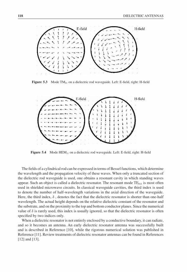
118 DIELECTRIC ANTENNAS
Figure 5.3 Mode TM01 on a dielectric rod waveguide. Left: E-field, right: H-field
Figure 5.4 Mode HEM11 on a dielectric rod waveguide. Left: E-field, right: H-field
The fields of a cylindrical rod can be expressed in terms of Bessel functions, which determinethe wavelength and the propagation velocity of these waves. When only a truncated section ofthe dielectric rod waveguide is used, one obtains a resonant cavity in which standing wavesappear. Such an object is called a dielectric resonator. The resonant mode TE01δ is most oftenused in shielded microwave circuits. In classical waveguide cavities, the third index is usedto denote the number of half-wavelength variations in the axial direction of the waveguide.Here, the third index, δ , denotes the fact that the dielectric resonator is shorter than one-halfwavelength. The actual height depends on the relative dielectric constant of the resonator andthe substrate, and on the proximity to the top and bottom conductor planes. Since the numericalvalue of δ is rarely used, this index is usually ignored, so that the dielectric resonator is oftenspecified by two indices only.
When a dielectric resonator is not entirely enclosed by a conductive boundary, it can radiate,and so it becomes an antenna. An early dielectric resonator antenna was successfully builtand is described in Reference [10], while the rigorous numerical solution was published inReference [11]. Review treatments of dielectric resonator antennas can be found in References[12] and [13].
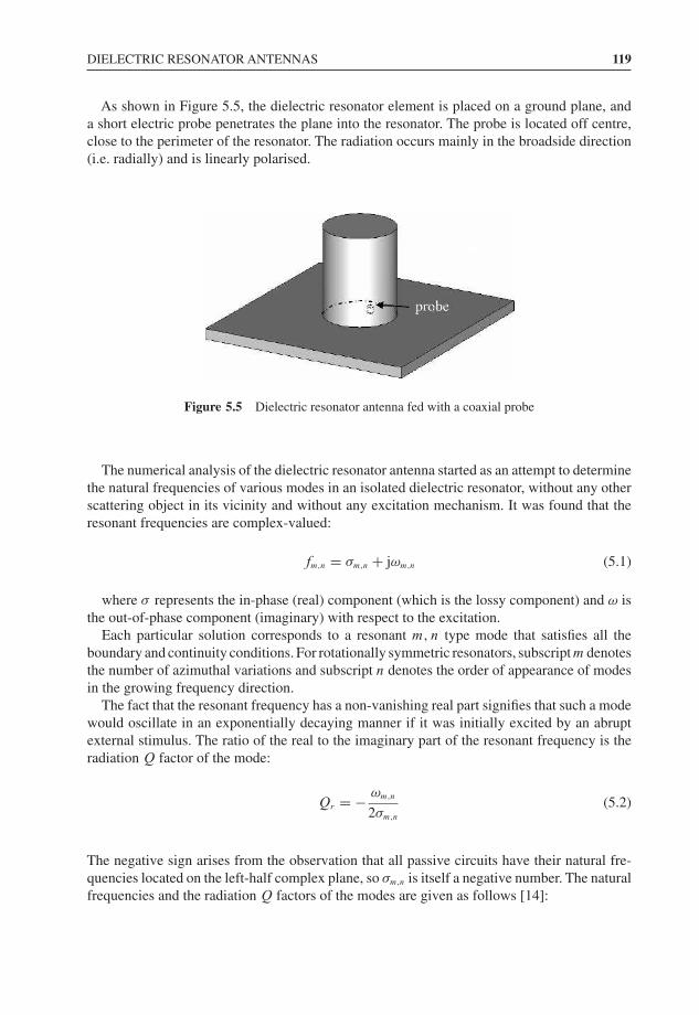
DIELECTRIC RESONATOR ANTENNAS 119
As shown in Figure 5.5, the dielectric resonator element is placed on a ground plane, anda short electric probe penetrates the plane into the resonator. The probe is located off centre,close to the perimeter of the resonator. The radiation occurs mainly in the broadside direction(i.e. radially) and is linearly polarised.
Figure 5.5 Dielectric resonator antenna fed with a coaxial probe
The numerical analysis of the dielectric resonator antenna started as an attempt to determinethe natural frequencies of various modes in an isolated dielectric resonator, without any otherscattering object in its vicinity and without any excitation mechanism. It was found that theresonant frequencies are complex-valued:
fm,n = σm,n + jωm,n (5.1)
where σ represents the in-phase (real) component (which is the lossy component) and ω isthe out-of-phase component (imaginary) with respect to the excitation.
Each particular solution corresponds to a resonant m, n type mode that satisfies all theboundary and continuity conditions. For rotationally symmetric resonators, subscript m denotesthe number of azimuthal variations and subscript n denotes the order of appearance of modesin the growing frequency direction.
The fact that the resonant frequency has a non-vanishing real part signifies that such a modewould oscillate in an exponentially decaying manner if it was initially excited by an abruptexternal stimulus. The ratio of the real to the imaginary part of the resonant frequency is theradiation Q factor of the mode:
Qr = − ωm,n
2σm,n
(5.2)
The negative sign arises from the observation that all passive circuits have their natural fre-quencies located on the left-half complex plane, so σm,n is itself a negative number. The naturalfrequencies and the radiation Q factors of the modes are given as follows [14]:
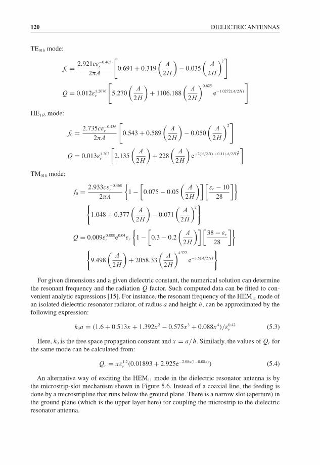
120 DIELECTRIC ANTENNAS
TE01� mode:
f0 = 2.921cε−0.465r
2πA
[0.691 + 0.319
(A
2H
)− 0.035
(A
2H
)2]
Q = 0.012ε1.2076r
[5.270
(A
2H
)+ 1106.188
(A
2H
)0.625
e−1.0272(A/2H)
]
HE11� mode:
f0 = 2.735cε−0.436r
2πA
[0.543 + 0.589
(A
2H
)− 0.050
(A
2H
)2]
Q = 0.013ε1.202r
[2.135
(A
2H
)+ 228
(A
2H
)e−2(A/2H) + 0.11(A/2H)2
]
TM01� mode:
f0 = 2.933cε−0.468r
2πA
{1 −
[0.075 − 0.05
(A
2H
)] [εr − 10
28
]}
{1.048 + 0.377
(A
2H
)− 0.071
(A
2H
)2}
Q = 0.009ε0.888r
e0.04εr
{1 −
[0.3 − 0.2
(A
2H
)] [38 − εr
28
]}
{9.498
(A
2H
)+ 2058.33
(A
2H
)4.322
e−3.5(A/2H)
}
For given dimensions and a given dielectric constant, the numerical solution can determinethe resonant frequency and the radiation Q factor. Such computed data can be fitted to con-venient analytic expressions [15]. For instance, the resonant frequency of the HEM11 mode ofan isolated dielectric resonator radiator, of radius a and height h, can be approximated by thefollowing expression:
k0a = (1.6 + 0.513x + 1.392x2 − 0.575x3 + 0.088x4)/ε0.42r
(5.3)
Here, k0 is the free space propagation constant and x = a/h. Similarly, the values of Qr forthe same mode can be calculated from:
Qr = xε1.2r
(0.01893 + 2.925e−2.08x(1−0.08x)) (5.4)
An alternative way of exciting the HEM11 mode in the dielectric resonator antenna is bythe microstrip-slot mechanism shown in Figure 5.6. Instead of a coaxial line, the feeding isdone by a microstripline that runs below the ground plane. There is a narrow slot (aperture) inthe ground plane (which is the upper layer here) for coupling the microstrip to the dielectricresonator antenna.
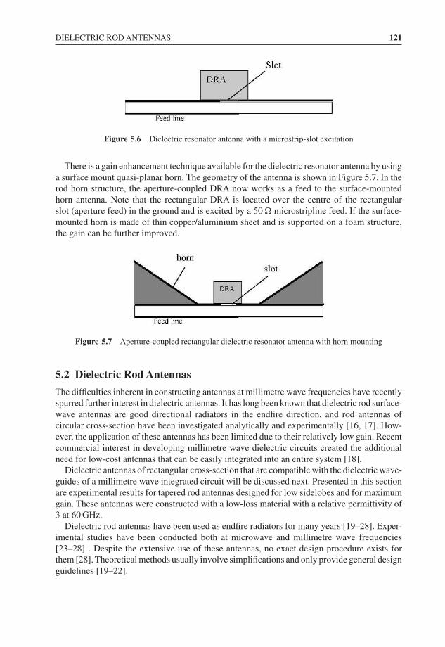
DIELECTRIC ROD ANTENNAS 121
Figure 5.6 Dielectric resonator antenna with a microstrip-slot excitation
There is a gain enhancement technique available for the dielectric resonator antenna by usinga surface mount quasi-planar horn. The geometry of the antenna is shown in Figure 5.7. In therod horn structure, the aperture-coupled DRA now works as a feed to the surface-mountedhorn antenna. Note that the rectangular DRA is located over the centre of the rectangularslot (aperture feed) in the ground and is excited by a 50 � microstripline feed. If the surface-mounted horn is made of thin copper/aluminium sheet and is supported on a foam structure,the gain can be further improved.
Figure 5.7 Aperture-coupled rectangular dielectric resonator antenna with horn mounting
5.2 Dielectric Rod Antennas
The difficulties inherent in constructing antennas at millimetre wave frequencies have recentlyspurred further interest in dielectric antennas. It has long been known that dielectric rod surface-wave antennas are good directional radiators in the endfire direction, and rod antennas ofcircular cross-section have been investigated analytically and experimentally [16, 17]. How-ever, the application of these antennas has been limited due to their relatively low gain. Recentcommercial interest in developing millimetre wave dielectric circuits created the additionalneed for low-cost antennas that can be easily integrated into an entire system [18].
Dielectric antennas of rectangular cross-section that are compatible with the dielectric wave-guides of a millimetre wave integrated circuit will be discussed next. Presented in this sectionare experimental results for tapered rod antennas designed for low sidelobes and for maximumgain. These antennas were constructed with a low-loss material with a relative permittivity of3 at 60 GHz.
Dielectric rod antennas have been used as endfire radiators for many years [19–28]. Exper-imental studies have been conducted both at microwave and millimetre wave frequencies[23–28] . Despite the extensive use of these antennas, no exact design procedure exists forthem [28]. Theoretical methods usually involve simplifications and only provide general designguidelines [19–22].
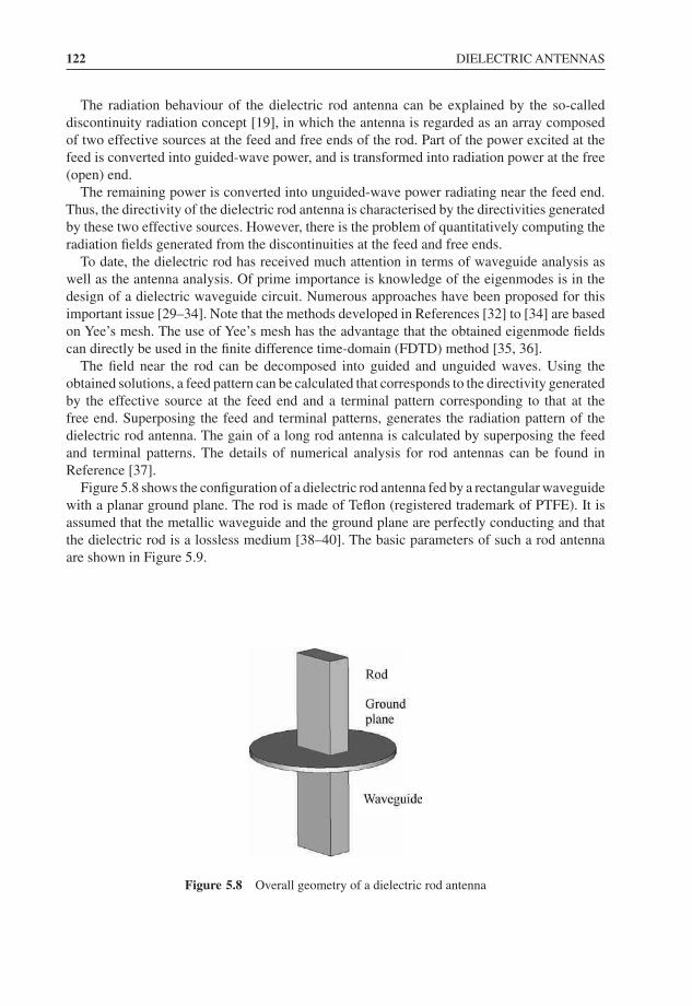
122 DIELECTRIC ANTENNAS
The radiation behaviour of the dielectric rod antenna can be explained by the so-calleddiscontinuity radiation concept [19], in which the antenna is regarded as an array composedof two effective sources at the feed and free ends of the rod. Part of the power excited at thefeed is converted into guided-wave power, and is transformed into radiation power at the free(open) end.
The remaining power is converted into unguided-wave power radiating near the feed end.Thus, the directivity of the dielectric rod antenna is characterised by the directivities generatedby these two effective sources. However, there is the problem of quantitatively computing theradiation fields generated from the discontinuities at the feed and free ends.
To date, the dielectric rod has received much attention in terms of waveguide analysis aswell as the antenna analysis. Of prime importance is knowledge of the eigenmodes is in thedesign of a dielectric waveguide circuit. Numerous approaches have been proposed for thisimportant issue [29–34]. Note that the methods developed in References [32] to [34] are basedon Yee’s mesh. The use of Yee’s mesh has the advantage that the obtained eigenmode fieldscan directly be used in the finite difference time-domain (FDTD) method [35, 36].
The field near the rod can be decomposed into guided and unguided waves. Using theobtained solutions, a feed pattern can be calculated that corresponds to the directivity generatedby the effective source at the feed end and a terminal pattern corresponding to that at thefree end. Superposing the feed and terminal patterns, generates the radiation pattern of thedielectric rod antenna. The gain of a long rod antenna is calculated by superposing the feedand terminal patterns. The details of numerical analysis for rod antennas can be found inReference [37].
Figure 5.8 shows the configuration of a dielectric rod antenna fed by a rectangular waveguidewith a planar ground plane. The rod is made of Teflon (registered trademark of PTFE). It isassumed that the metallic waveguide and the ground plane are perfectly conducting and thatthe dielectric rod is a lossless medium [38–40]. The basic parameters of such a rod antennaare shown in Figure 5.9.
Figure 5.8 Overall geometry of a dielectric rod antenna
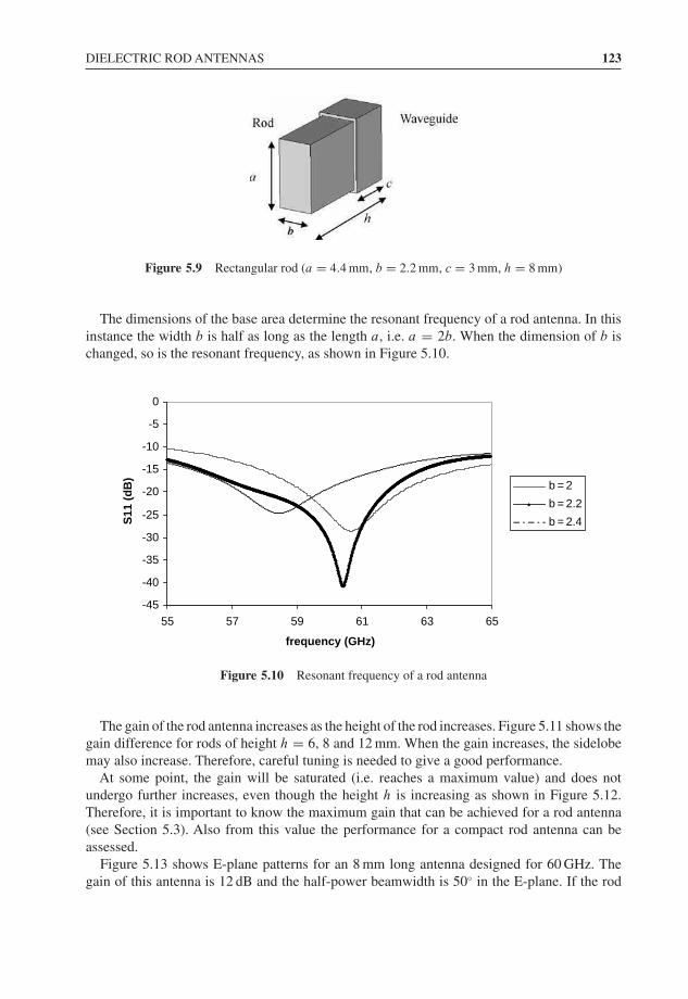
DIELECTRIC ROD ANTENNAS 123
Figure 5.9 Rectangular rod (a = 4.4 mm, b = 2.2 mm, c = 3 mm, h = 8 mm)
The dimensions of the base area determine the resonant frequency of a rod antenna. In thisinstance the width b is half as long as the length a, i.e. a = 2b. When the dimension of b ischanged, so is the resonant frequency, as shown in Figure 5.10.
-45
-40
-35
-30
-25
-20
-15
-10
-5
0
55 57 59 61 63 65
frequency (GHz)
S11
(d
B)
b = 2
b = 2.2
b = 2.4
Figure 5.10 Resonant frequency of a rod antenna
The gain of the rod antenna increases as the height of the rod increases. Figure 5.11 shows thegain difference for rods of height h = 6, 8 and 12 mm. When the gain increases, the sidelobemay also increase. Therefore, careful tuning is needed to give a good performance.
At some point, the gain will be saturated (i.e. reaches a maximum value) and does notundergo further increases, even though the height h is increasing as shown in Figure 5.12.Therefore, it is important to know the maximum gain that can be achieved for a rod antenna(see Section 5.3). Also from this value the performance for a compact rod antenna can beassessed.
Figure 5.13 shows E-plane patterns for an 8 mm long antenna designed for 60 GHz. Thegain of this antenna is 12 dB and the half-power beamwidth is 50◦ in the E-plane. If the rod
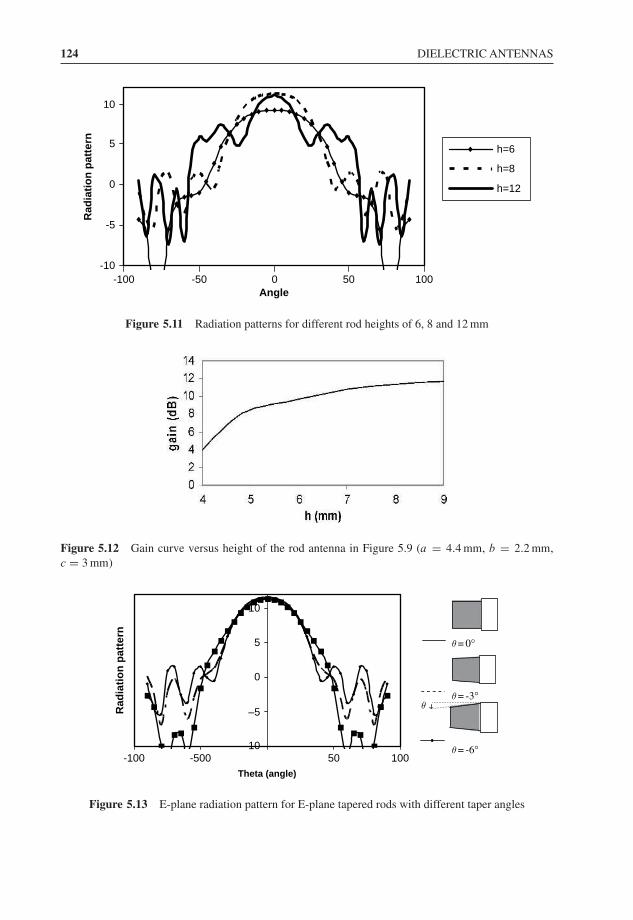
124 DIELECTRIC ANTENNAS
-10
-5
0
5
10
Angle
Rad
iati
on
pat
tern
h=6
h=8
h=12
-100 -50 0 50 100
Figure 5.11 Radiation patterns for different rod heights of 6, 8 and 12 mm
Figure 5.12 Gain curve versus height of the rod antenna in Figure 5.9 (a = 4.4 mm, b = 2.2 mm,c = 3 mm)
–10
–5
0
5
10
-100 -500 50 100Theta (angle)
Rad
iati
on
pat
tern
θ = -3°
θ = 0°
θ = -6°
θ
Figure 5.13 E-plane radiation pattern for E-plane tapered rods with different taper angles
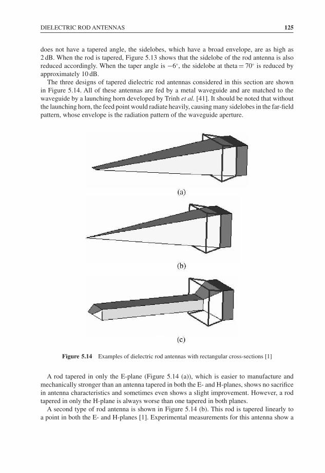
DIELECTRIC ROD ANTENNAS 125
does not have a tapered angle, the sidelobes, which have a broad envelope, are as high as2 dB. When the rod is tapered, Figure 5.13 shows that the sidelobe of the rod antenna is alsoreduced accordingly. When the taper angle is −6◦, the sidelobe at theta = 70◦ is reduced byapproximately 10 dB.
The three designs of tapered dielectric rod antennas considered in this section are shownin Figure 5.14. All of these antennas are fed by a metal waveguide and are matched to thewaveguide by a launching horn developed by Trinh et al. [41]. It should be noted that withoutthe launching horn, the feed point would radiate heavily, causing many sidelobes in the far-fieldpattern, whose envelope is the radiation pattern of the waveguide aperture.
Figure 5.14 Examples of dielectric rod antennas with rectangular cross-sections [1]
A rod tapered in only the E-plane (Figure 5.14 (a)), which is easier to manufacture andmechanically stronger than an antenna tapered in both the E- and H-planes, shows no sacrificein antenna characteristics and sometimes even shows a slight improvement. However, a rodtapered in only the H-plane is always worse than one tapered in both planes.
A second type of rod antenna is shown in Figure 5.14 (b). This rod is tapered linearly toa point in both the E- and H-planes [1]. Experimental measurements for this antenna show a
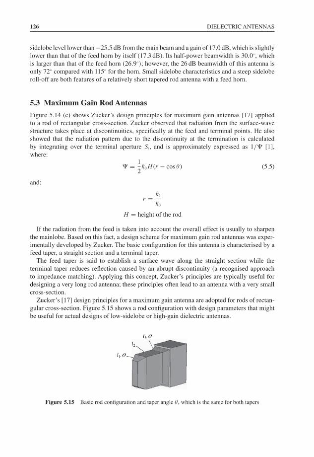
126 DIELECTRIC ANTENNAS
sidelobe level lower than −25.5 dB from the main beam and a gain of 17.0 dB, which is slightlylower than that of the feed horn by itself (17.3 dB). Its half-power beamwidth is 30.0◦, whichis larger than that of the feed horn (26.9◦); however, the 26 dB beamwidth of this antenna isonly 72◦ compared with 115◦ for the horn. Small sidelobe characteristics and a steep sideloberoll-off are both features of a relatively short tapered rod antenna with a feed horn.
5.3 Maximum Gain Rod Antennas
Figure 5.14 (c) shows Zucker’s design principles for maximum gain antennas [17] appliedto a rod of rectangular cross-section. Zucker observed that radiation from the surface-wavestructure takes place at discontinuities, specifically at the feed and terminal points. He alsoshowed that the radiation pattern due to the discontinuity at the termination is calculatedby integrating over the terminal aperture St , and is approximately expressed as 1/� [1],where:
� = 1
2k0H(r − cos θ) (5.5)
and:
r = k2
k0
H = height of the rod
If the radiation from the feed is taken into account the overall effect is usually to sharpenthe mainlobe. Based on this fact, a design scheme for maximum gain rod antennas was exper-imentally developed by Zucker. The basic configuration for this antenna is characterised by afeed taper, a straight section and a terminal taper.
The feed taper is said to establish a surface wave along the straight section while theterminal taper reduces reflection caused by an abrupt discontinuity (a recognised approachto impedance matching). Applying this concept, Zucker’s principles are typically useful fordesigning a very long rod antenna; these principles often lead to an antenna with a very smallcross-section.
Zucker’s [17] design principles for a maximum gain antenna are adopted for rods of rectan-gular cross-section. Figure 5.15 shows a rod configuration with design parameters that mightbe useful for actual designs of low-sidelobe or high-gain dielectric antennas.
l1, θ
l2
l3, θ
Figure 5.15 Basic rod configuration and taper angle θ , which is the same for both tapers
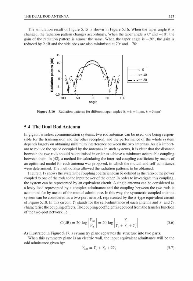
THE DUAL ROD ANTENNA 127
The simulation result of Figure 5.15 is shown in Figure 5.16. When the taper angle θ ischanged, the radiation pattern changes accordingly. When the taper angle is 0◦ and −10◦, thegain of the radiation pattern is almost the same. When the taper angle is −20◦, the gain isreduced by 2 dB and the sidelobes are also minimised at 70◦ and −70◦.
-10
-5
0
5
10
15
-100 -50 0 50 100angle
Rad
iati
on
pat
tern
(d
B)
e=0
e=-10
e=-20
Figure 5.16 Radiation patterns for different taper angles (l1 = l3 =1 mm, l2 =3 mm)
5.4 The Dual Rod Antenna
In gigabit wireless communication systems, two rod antennas can be used, one being respon-sible for the transmission and the other reception, and the performance of the whole systemdepends largely on obtaining minimum interference between the two antennas. As it is import-ant to reduce the space occupied by the antennas in such systems, it is clear that the distancebetween the two rods should be optimised in order to achieve a minimum acceptable couplingbetween them. In [42], a method for calculating the inter-rod coupling coefficient by means ofan optimised model for each antenna was proposed, in which the mutual and self-admittancewere determined. The method also allowed the radiation patterns to be obtained.
Figure 5.17 shows the system the coupling coefficient can be defined as the ratio of the powercoupled to one of the rods to the input power of the other. In order to investigate this coupling,the system can be represented by an equivalent circuit. A single antenna can be considered asa lossy load represented by a complex admittance and the coupling between the two rods isaccounted for by means of the mutual admittance. In this way, the symmetric coupled antennasystem can be considered as a two-port network represented by the π -type equivalent circuitof Figure 5.18. In this circuit, Y0 stands for the self-admittance of each antenna and Y1 and Y2
characterise the coupling effects. The coupling coefficient is deduced from the transfer functionof the two-port network i.e.:
C(dB) = 20 log
∣∣∣∣Vout
Vin
∣∣∣∣ = 20 log
∣∣∣∣ Y1
Y0 + Y1 + Y2
∣∣∣∣ (5.6)
As illustrated in Figure 5.17, a symmetry plane separates the structure into two parts.When this symmetry plane is an electric wall, the input equivalent admittance will be the
odd admittance given by:Yodd = Y0 + Y2 + 2Y1 (5.7)
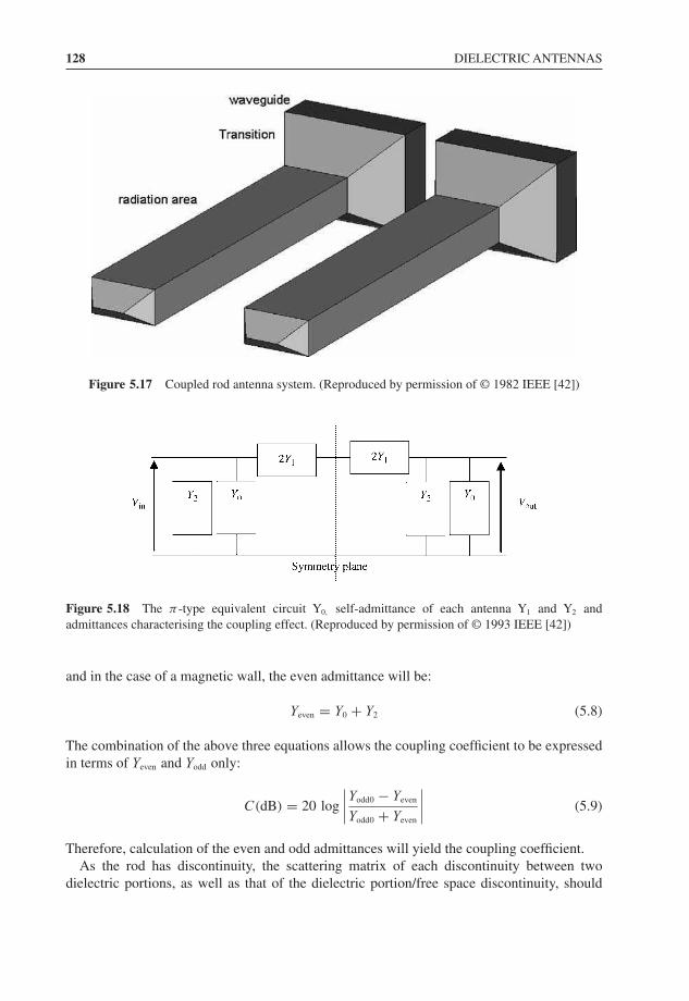
128 DIELECTRIC ANTENNAS
Figure 5.17 Coupled rod antenna system. (Reproduced by permission of © 1982 IEEE [42])
Figure 5.18 The π -type equivalent circuit Y0, self-admittance of each antenna Y1 and Y2 andadmittances characterising the coupling effect. (Reproduced by permission of © 1993 IEEE [42])
and in the case of a magnetic wall, the even admittance will be:
Yeven = Y0 + Y2 (5.8)
The combination of the above three equations allows the coupling coefficient to be expressedin terms of Yeven and Yodd only:
C(dB) = 20 log
∣∣∣∣Yodd0 − Yeven
Yodd0 + Yeven
∣∣∣∣ (5.9)
Therefore, calculation of the even and odd admittances will yield the coupling coefficient.As the rod has discontinuity, the scattering matrix of each discontinuity between two
dielectric portions, as well as that of the dielectric portion/free space discontinuity, should
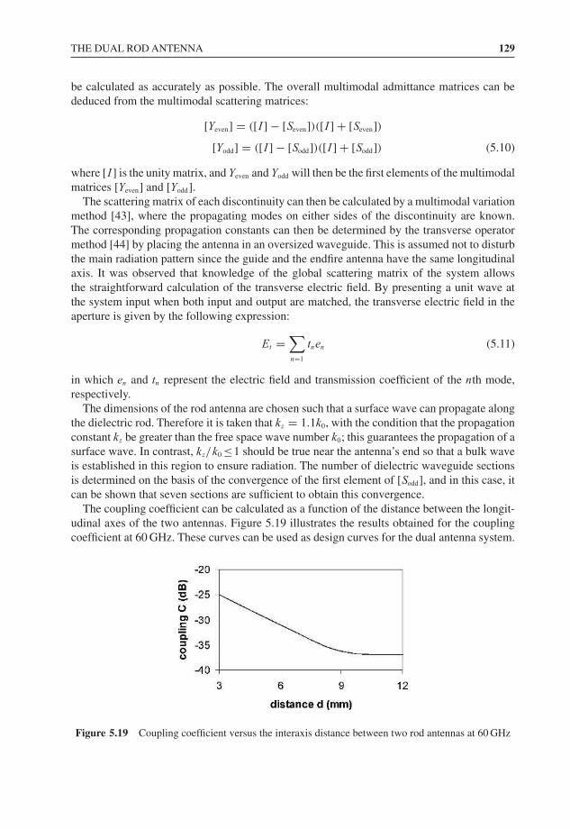
THE DUAL ROD ANTENNA 129
be calculated as accurately as possible. The overall multimodal admittance matrices can bededuced from the multimodal scattering matrices:
[Yeven] = ([I ] − [Seven])([I ] + [Seven])[Yodd] = ([I ] − [Sodd])([I ] + [Sodd]) (5.10)
where [I ] is the unity matrix, and Yeven and Yodd will then be the first elements of the multimodalmatrices [Yeven] and [Yodd].
The scattering matrix of each discontinuity can then be calculated by a multimodal variationmethod [43], where the propagating modes on either sides of the discontinuity are known.The corresponding propagation constants can then be determined by the transverse operatormethod [44] by placing the antenna in an oversized waveguide. This is assumed not to disturbthe main radiation pattern since the guide and the endfire antenna have the same longitudinalaxis. It was observed that knowledge of the global scattering matrix of the system allowsthe straightforward calculation of the transverse electric field. By presenting a unit wave atthe system input when both input and output are matched, the transverse electric field in theaperture is given by the following expression:
Et =∑n=1
tnen (5.11)
in which en and tn represent the electric field and transmission coefficient of the nth mode,respectively.
The dimensions of the rod antenna are chosen such that a surface wave can propagate alongthe dielectric rod. Therefore it is taken that kz = 1.1k0, with the condition that the propagationconstant kz be greater than the free space wave number k0; this guarantees the propagation of asurface wave. In contrast, kz/k0 ≤1 should be true near the antenna’s end so that a bulk waveis established in this region to ensure radiation. The number of dielectric waveguide sectionsis determined on the basis of the convergence of the first element of [Sodd], and in this case, itcan be shown that seven sections are sufficient to obtain this convergence.
The coupling coefficient can be calculated as a function of the distance between the longit-udinal axes of the two antennas. Figure 5.19 illustrates the results obtained for the couplingcoefficient at 60 GHz. These curves can be used as design curves for the dual antenna system.
Figure 5.19 Coupling coefficient versus the interaxis distance between two rod antennas at 60 GHz
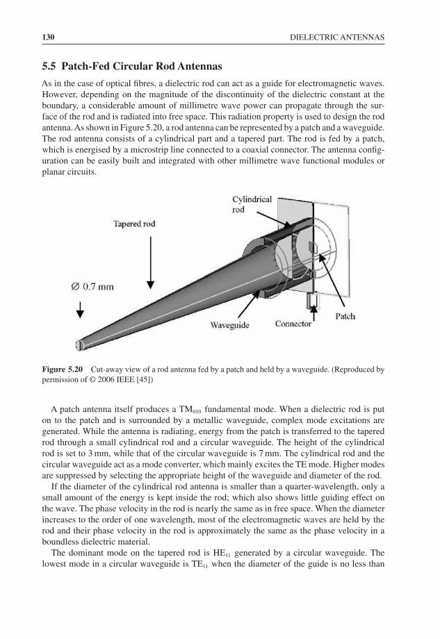
130 DIELECTRIC ANTENNAS
5.5 Patch-Fed Circular Rod Antennas
As in the case of optical fibres, a dielectric rod can act as a guide for electromagnetic waves.However, depending on the magnitude of the discontinuity of the dielectric constant at theboundary, a considerable amount of millimetre wave power can propagate through the sur-face of the rod and is radiated into free space. This radiation property is used to design the rodantenna.As shown in Figure 5.20, a rod antenna can be represented by a patch and a waveguide.The rod antenna consists of a cylindrical part and a tapered part. The rod is fed by a patch,which is energised by a microstrip line connected to a coaxial connector. The antenna config-uration can be easily built and integrated with other millimetre wave functional modules orplanar circuits.
Figure 5.20 Cut-away view of a rod antenna fed by a patch and held by a waveguide. (Reproduced bypermission of © 2006 IEEE [45])
A patch antenna itself produces a TM010 fundamental mode. When a dielectric rod is puton to the patch and is surrounded by a metallic waveguide, complex mode excitations aregenerated. While the antenna is radiating, energy from the patch is transferred to the taperedrod through a small cylindrical rod and a circular waveguide. The height of the cylindricalrod is set to 3 mm, while that of the circular waveguide is 7 mm. The cylindrical rod and thecircular waveguide act as a mode converter, which mainly excites the TE mode. Higher modesare suppressed by selecting the appropriate height of the waveguide and diameter of the rod.
If the diameter of the cylindrical rod antenna is smaller than a quarter-wavelength, only asmall amount of the energy is kept inside the rod; which also shows little guiding effect onthe wave. The phase velocity in the rod is nearly the same as in free space. When the diameterincreases to the order of one wavelength, most of the electromagnetic waves are held by therod and their phase velocity in the rod is approximately the same as the phase velocity in aboundless dielectric material.
The dominant mode on the tapered rod is HE11 generated by a circular waveguide. Thelowest mode in a circular waveguide is TE11 when the diameter of the guide is no less than
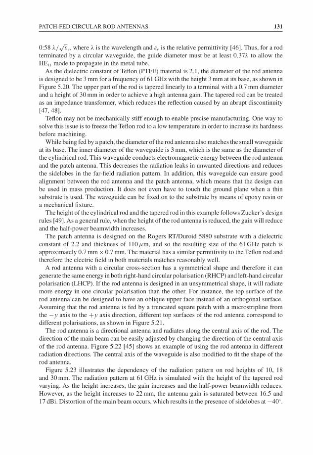
PATCH-FED CIRCULAR ROD ANTENNAS 131
0:58 λ/√
εr , where λ is the wavelength and εr is the relative permittivity [46]. Thus, for a rodterminated by a circular waveguide, the guide diameter must be at least 0.37λ to allow theHE11 mode to propagate in the metal tube.
As the dielectric constant of Teflon (PTFE) material is 2.1, the diameter of the rod antennais designed to be 3 mm for a frequency of 61 GHz with the height 3 mm at its base, as shown inFigure 5.20. The upper part of the rod is tapered linearly to a terminal with a 0.7 mm diameterand a height of 30 mm in order to achieve a high antenna gain. The tapered rod can be treatedas an impedance transformer, which reduces the reflection caused by an abrupt discontinuity[47, 48].
Teflon may not be mechanically stiff enough to enable precise manufacturing. One way tosolve this issue is to freeze the Teflon rod to a low temperature in order to increase its hardnessbefore machining.
While being fed by a patch, the diameter of the rod antenna also matches the small waveguideat its base. The inner diameter of the waveguide is 3 mm, which is the same as the diameter ofthe cylindrical rod. This waveguide conducts electromagnetic energy between the rod antennaand the patch antenna. This decreases the radiation leaks in unwanted directions and reducesthe sidelobes in the far-field radiation pattern. In addition, this waveguide can ensure goodalignment between the rod antenna and the patch antenna, which means that the design canbe used in mass production. It does not even have to touch the ground plane when a thinsubstrate is used. The waveguide can be fixed on to the substrate by means of epoxy resin ora mechanical fixture.
The height of the cylindrical rod and the tapered rod in this example follows Zucker’s designrules [49]. As a general rule, when the height of the rod antenna is reduced, the gain will reduceand the half-power beamwidth increases.
The patch antenna is designed on the Rogers RT/Duroid 5880 substrate with a dielectricconstant of 2.2 and thickness of 110 μm, and so the resulting size of the 61 GHz patch isapproximately 0.7 mm × 0.7 mm. The material has a similar permittivity to the Teflon rod andtherefore the electric field in both materials matches reasonably well.
A rod antenna with a circular cross-section has a symmetrical shape and therefore it cangenerate the same energy in both right-hand circular polarisation (RHCP) and left-hand circularpolarisation (LHCP). If the rod antenna is designed in an unsymmetrical shape, it will radiatemore energy in one circular polarisation than the other. For instance, the top surface of therod antenna can be designed to have an oblique upper face instead of an orthogonal surface.Assuming that the rod antenna is fed by a truncated square patch with a microstripline fromthe −y axis to the +y axis direction, different top surfaces of the rod antenna correspond todifferent polarisations, as shown in Figure 5.21.
The rod antenna is a directional antenna and radiates along the central axis of the rod. Thedirection of the main beam can be easily adjusted by changing the direction of the central axisof the rod antenna. Figure 5.22 [45] shows an example of using the rod antenna in differentradiation directions. The central axis of the waveguide is also modified to fit the shape of therod antenna.
Figure 5.23 illustrates the dependency of the radiation pattern on rod heights of 10, 18and 30 mm. The radiation pattern at 61 GHz is simulated with the height of the tapered rodvarying. As the height increases, the gain increases and the half-power beamwidth reduces.However, as the height increases to 22 mm, the antenna gain is saturated between 16.5 and17 dBi. Distortion of the main beam occurs, which results in the presence of sidelobes at −40◦.
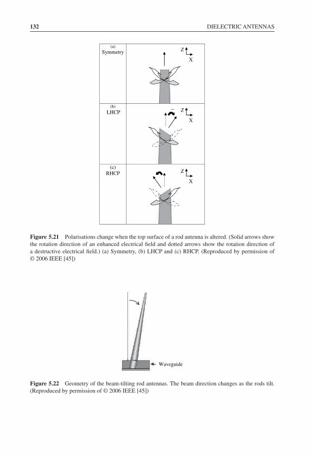
132 DIELECTRIC ANTENNAS
(a)Symmetry
(b)
LHCP
(c)RHCP
–
Z
X
Z
X
Z
X
Figure 5.21 Polarisations change when the top surface of a rod antenna is altered. (Solid arrows showthe rotation direction of an enhanced electrical field and dotted arrows show the rotation direction ofa destructive electrical field.) (a) Symmetry, (b) LHCP and (c) RHCP. (Reproduced by permission of© 2006 IEEE [45])
Waveguide
Figure 5.22 Geometry of the beam-tilting rod antennas. The beam direction changes as the rods tilt.(Reproduced by permission of © 2006 IEEE [45])
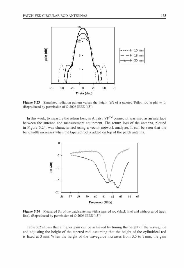
PATCH-FED CIRCULAR ROD ANTENNAS 133
0
4
8
12
16
-75 -50 -25 0 25 50 75
Theta (deg)
gai
n (
dB
)
H=10 mm
H=18 mm
H=30 mm
Figure 5.23 Simulated radiation pattern versus the height (H ) of a tapered Teflon rod at phi = 0.(Reproduced by permission of © 2006 IEEE [45])
In this work, to measure the return loss, an Anritsu VPTM connector was used as an interfacebetween the antenna and measurement equipment. The return loss of the antenna, plottedin Figure 5.24, was characterised using a vector network analyser. It can be seen that thebandwidth increases when the tapered rod is added on top of the patch antenna.
-20
-15
-10
-5
0
56 57 58 59 60 61 62 63 64 65
Frequency (GHz)
S11
(dB
)
Figure 5.24 Measured S11 of the patch antenna with a tapered rod (black line) and without a rod (greyline). (Reproduced by permission of © 2006 IEEE [45])
Table 5.2 shows that a higher gain can be achieved by tuning the height of the waveguideand adjusting the height of the tapered rod, assuming that the height of the cylindrical rodis fixed at 3 mm. When the height of the waveguide increases from 3.5 to 7 mm, the gain
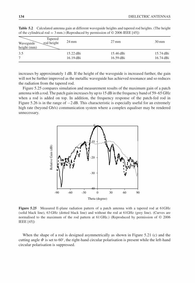
134 DIELECTRIC ANTENNAS
Table 5.2 Calculated antenna gain at different waveguide heights and tapered rod heights. (The heightof the cylindrical rod = 3 mm.) (Reproduced by permission of © 2006 IEEE [45])
Waveguideheight (mm)
Taperedrod height 24 mm 27 mm 30 mm
3.5 15.22 dBi 15.46 dBi 15.74 dBi7 16.19 dBi 16.59 dBi 16.74 dBi
increases by approximately 1 dB. If the height of the waveguide is increased further, the gainwill not be further improved as the metallic waveguide has achieved resonance and so reducesthe radiation from the tapered rod.
Figure 5.25 compares simulation and measurement results of the maximum gain of a patchantenna with a rod. The patch gain increases by up to 15 dB in the frequency band of 59–65 GHzwhen a rod is added on top. In addition, the frequency response of the patch-fed rod inFigure 5.26 is in the range of −2 dB. This characteristic is especially useful for an extremelyhigh rate (beyond Gb/s) communication system where a complex equaliser may be renderedunnecessary.
-40
-30
-20
-10
0
-90 -60 -30 0 30 60 90
Theta (degree)
Rel
ativ
e G
ain
(dB
)
Figure 5.25 Measured E-plane radiation pattern of a patch antenna with a tapered rod at 61GHz(solid black line), 63 GHz (dotted black line) and without the rod at 61GHz (grey line). (Curves arenormalised to the maximum of the rod pattern at 61 GHz.) (Reproduced by permission of © 2006IEEE [45])
When the shape of a rod is designed asymmetrically as shown in Figure 5.21 (c) and thecutting angle Φ is set to 60◦, the right-hand circular polarisation is present while the left-handcircular polarisation is suppressed.
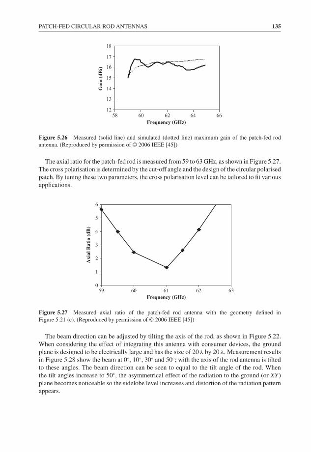
PATCH-FED CIRCULAR ROD ANTENNAS 135
5812
13
14
15
16
17
18
60 62 64 66Frequency (GHz)
Gai
n (d
Bi)
Figure 5.26 Measured (solid line) and simulated (dotted line) maximum gain of the patch-fed rodantenna. (Reproduced by permission of © 2006 IEEE [45])
The axial ratio for the patch-fed rod is measured from 59 to 63 GHz, as shown in Figure 5.27.The cross polarisation is determined by the cut-off angle and the design of the circular polarisedpatch. By tuning these two parameters, the cross polarisation level can be tailored to fit variousapplications.
590
1
2
3
4
5
6
60 61 62 63Frequency (GHz)
Axi
al R
atio
(dB
)
Figure 5.27 Measured axial ratio of the patch-fed rod antenna with the geometry defined inFigure 5.21 (c). (Reproduced by permission of © 2006 IEEE [45])
The beam direction can be adjusted by tilting the axis of the rod, as shown in Figure 5.22.When considering the effect of integrating this antenna with consumer devices, the groundplane is designed to be electrically large and has the size of 20 λ by 20 λ. Measurement resultsin Figure 5.28 show the beam at 0◦, 10◦, 30◦ and 50◦; with the axis of the rod antenna is tiltedto these angles. The beam direction can be seen to equal to the tilt angle of the rod. Whenthe tilt angles increase to 50◦, the asymmetrical effect of the radiation to the ground (or XY )plane becomes noticeable so the sidelobe level increases and distortion of the radiation patternappears.
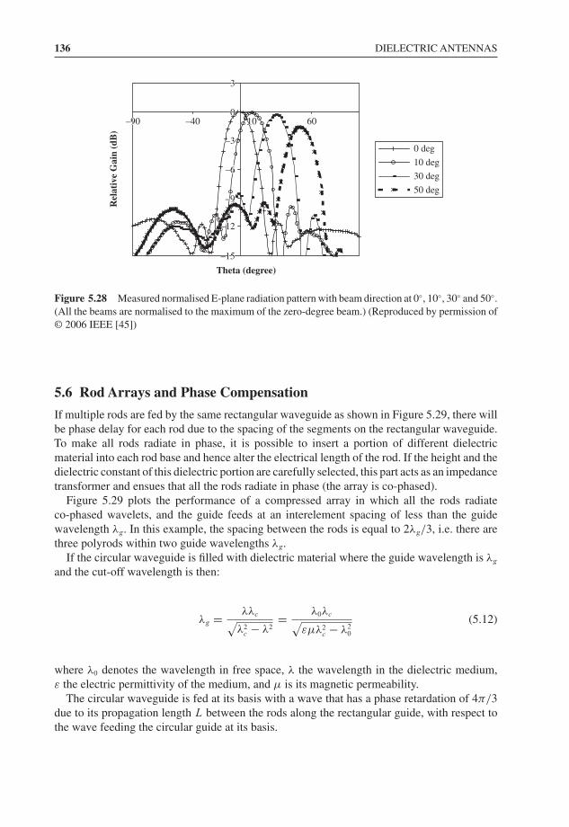
136 DIELECTRIC ANTENNAS
–15
–12
–9
–6
–3
0
3
–90 –40 10 60
Theta (degree)
Rel
ativ
e G
ain
(dB
)
0 deg
10 deg
30 deg
50 deg
Figure 5.28 Measured normalised E-plane radiation pattern with beam direction at 0◦, 10◦, 30◦ and 50◦.(All the beams are normalised to the maximum of the zero-degree beam.) (Reproduced by permission of© 2006 IEEE [45])
5.6 Rod Arrays and Phase Compensation
If multiple rods are fed by the same rectangular waveguide as shown in Figure 5.29, there willbe phase delay for each rod due to the spacing of the segments on the rectangular waveguide.To make all rods radiate in phase, it is possible to insert a portion of different dielectricmaterial into each rod base and hence alter the electrical length of the rod. If the height and thedielectric constant of this dielectric portion are carefully selected, this part acts as an impedancetransformer and ensues that all the rods radiate in phase (the array is co-phased).
Figure 5.29 plots the performance of a compressed array in which all the rods radiateco-phased wavelets, and the guide feeds at an interelement spacing of less than the guidewavelength λg. In this example, the spacing between the rods is equal to 2λg/3, i.e. there arethree polyrods within two guide wavelengths λg.
If the circular waveguide is filled with dielectric material where the guide wavelength is λg
and the cut-off wavelength is then:
λg = λλc√λ2
c− λ2
= λ0λc√εμλ2
c− λ2
0
(5.12)
where λ0 denotes the wavelength in free space, λ the wavelength in the dielectric medium,ε the electric permittivity of the medium, and μ is its magnetic permeability.
The circular waveguide is fed at its basis with a wave that has a phase retardation of 4π/3due to its propagation length L between the rods along the rectangular guide, with respect tothe wave feeding the circular guide at its basis.
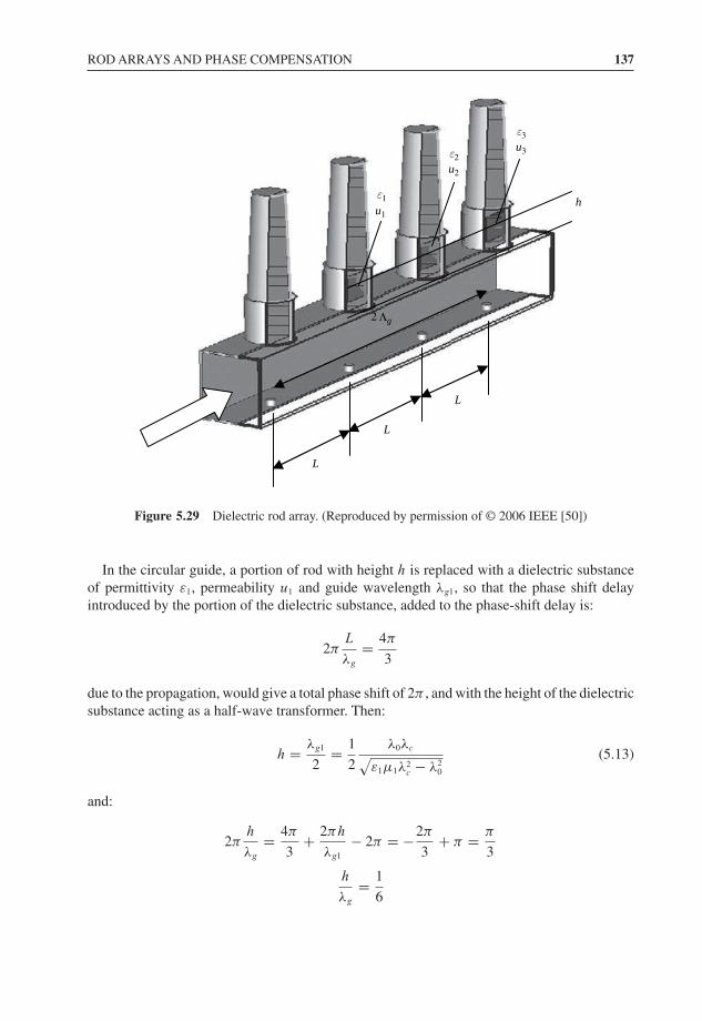
ROD ARRAYS AND PHASE COMPENSATION 137
h
2 Λg
L
L
L
ε1
ε2
u1
u2
ε3
u3
Figure 5.29 Dielectric rod array. (Reproduced by permission of © 2006 IEEE [50])
In the circular guide, a portion of rod with height h is replaced with a dielectric substanceof permittivity ε1, permeability u1 and guide wavelength λg1, so that the phase shift delayintroduced by the portion of the dielectric substance, added to the phase-shift delay is:
2πL
λg
= 4π
3
due to the propagation, would give a total phase shift of 2π , and with the height of the dielectricsubstance acting as a half-wave transformer. Then:
h = λg1
2= 1
2
λ0λc√ε1μ1λ2
c− λ2
0
(5.13)
and:
2πh
λg
= 4π
3+ 2πh
λg1
− 2π = −2π
3+ π = π
3
h
λg
= 1
6

138 DIELECTRIC ANTENNAS
By substituting to h and to λg from their respective expressions embodied in Equations (5.12)and (5.13):
√εμλ2
c− λ2
0
2√
ε1μ1λ2c− λ2
0
= 1
6
ε1μ1 = εμ − 8
(λ0
λc
)2
Assuming μ1 =μ=1:
ε1 = ε − 8
(λ0
λc
)2
By choosing a wavelength in free space:
λ0 = 3.34 mm
and a circular guide of a radius of 1.6 mm, and therefore a cut-off wavelength of:
λc = 1.6 × 1.7 = 2.72 mm
corresponding to a wave H11, and by taking:
ε = 2.25
therefore:
ε1 = 9 × 2.25 − 8
(3.34
2.72
)2
= 8.15
h = 0.65 mm
In the same manner, in the circular guide, a portion of a dielectric substance will be insertedwith height h, permittivity ε2 and permeability μ2 and a guide wavelength λg2 so that thephase-shift delay introduced by this portion of the dielectric substance, added to the phase-shiftdelay is:
2π2L
λ2
= 8π
3
due to the propagation, would give a total phase shift of 4π , and the height of the dielectricsubstance will act as a three-halves wave transformer. Then:
h = 3λg2
2= 3λcλ0
2√
ε2μ2λ2c− λ2
0
(5.14)
and:
2πh
λg
= 8π
3+ 2πh
λg2
− 4π = −4π
3+ 3π = 5π
3
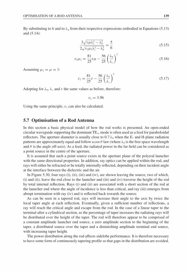
OPTIMISATION OF A ROD ANTENNA 139
By substituting to h and to λg from their respective expressions embodied in Equations (5.13)and (5.14):
3√
εμλ2c− λ2
0
2√
ε2μ2λ2c− λ2
0
= 5
6(5.15)
ε2μ2 = 81
25εμ − 56
25
(λ0
λc
)2
(5.16)
Assuming μ2 = μ = 1:
ε2 = 81
25ε − 56
25
(λ0
λc
)2
(5.17)
Adopting for λ0, λc and ε the same values as before, therefore:
ε2 = 3.96
Using the same principle, ε3 can also be calculated.
5.7 Optimisation of a Rod Antenna
In this section a basic physical model of how the rod works is presented. An open-endedcircular waveguide supporting the dominant TE11 mode is often used as a feed for paraboloidalreflectors. The aperture diameter is usually close to 0.7 λ0 when the E- and H-plane radiationpatterns are approximately equal and follow a cos θ law (where λ0 is the free space wavelengthand θ is the angle off-axis). As a feed, the radiated power in the far field can be considered asa point source in the centre of the aperture.
It is assumed that such a point source exists in the aperture plane of the polyrod launcherwith the same directional properties. In addition, ray optics can be applied within the rod, andrays will either be refracted or be totally internally reflected, depending on their incident angleat the interface between the dielectric and the air.
In Figure 5.30, four rays (i), (ii), (iii) and (iv), are shown leaving the source, two of which,(i) and (ii), leave the rod close to the launcher and (iii) and (iv) traverse the height of the rodby total internal reflection. Rays (i) and (ii) are associated with a short section of the rod atthe launcher end where the angle of incidence is less than critical, and ray (iii) emerges fromabrupt termination with ray (iv) and is reflected back towards the source.
As can be seen in a tapered rod, rays will increase their angle to the axis by twice thelocal taper angle at each reflection. Eventually, given a sufficient number of reflections, aray will reach the critical angle and escape from the rod. In the case of a linear taper to theterminal after a cylindrical section, as the percentage of taper increases the radiating rays willbe distributed over the height of the taper. The rod will therefore appear to be comprised ofa constant amplitude launcher end source, a zero amplitude section to the beginning of thetaper, a distributed source over the taper and a diminishing amplitude terminal end source,with increasing taper height.
The power distribution along the rod affects sidelobe performance. It is therefore necessaryto have some form of continuously tapering profile so that gaps in the distribution are avoided.
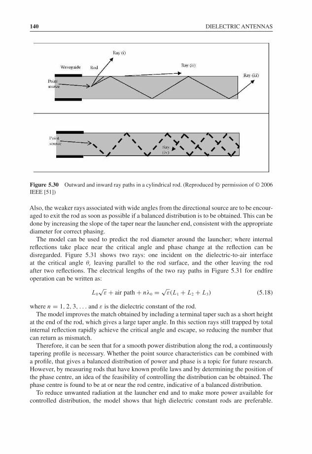
140 DIELECTRIC ANTENNAS
Figure 5.30 Outward and inward ray paths in a cylindrical rod. (Reproduced by permission of © 2006IEEE [51])
Also, the weaker rays associated with wide angles from the directional source are to be encour-aged to exit the rod as soon as possible if a balanced distribution is to be obtained. This can bedone by increasing the slope of the taper near the launcher end, consistent with the appropriatediameter for correct phasing.
The model can be used to predict the rod diameter around the launcher; where internalreflections take place near the critical angle and phase change at the reflection can bedisregarded. Figure 5.31 shows two rays: one incident on the dielectric-to-air interfaceat the critical angle θc leaving parallel to the rod surface, and the other leaving the rodafter two reflections. The electrical lengths of the two ray paths in Figure 5.31 for endfireoperation can be written as:
L0
√ε + air path + nλ0 = √
ε(L1 + L2 + L3) (5.18)
where n = 1, 2, 3, . . . and ε is the dielectric constant of the rod.The model improves the match obtained by including a terminal taper such as a short height
at the end of the rod, which gives a large taper angle. In this section rays still trapped by totalinternal reflection rapidly achieve the critical angle and escape, so reducing the number thatcan return as mismatch.
Therefore, it can be seen that for a smooth power distribution along the rod, a continuouslytapering profile is necessary. Whether the point source characteristics can be combined witha profile, that gives a balanced distribution of power and phase is a topic for future research.However, by measuring rods that have known profile laws and by determining the position ofthe phase centre, an idea of the feasibility of controlling the distribution can be obtained. Thephase centre is found to be at or near the rod centre, indicative of a balanced distribution.
To reduce unwanted radiation at the launcher end and to make more power available forcontrolled distribution, the model shows that high dielectric constant rods are preferable.
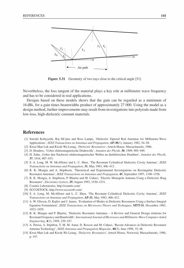
REFERENCES 141
Air path
L0 θc
θcL1 L2
L3
Figure 5.31 Geometry of two rays close to the critical angle [51]
Nevertheless, the loss tangent of the material plays a key role at millimetre wave frequencyand has to be considered in real applications.
Designs based on these models shows that the gain can be regarded as a minimum of16 dBi, for a gain times beamwidths product of approximately 27 000. Using the model as adesign method, further improvements may result from investigations into polyrods made fromlow-loss, high-dielectric constant materials.
References[1] Satoshi Kobayashi, Raj Mi’ptra and Ross Lampe, ‘Dielectric Tapered Rod Antennas for Millimetre-Wave
Applications’, IEEE Transactions on Antennas and Propagation, AP-30(1), January 1982, 54–58.[2] Kwai-Man Luk and Kwok-Wa Leung, ‘Dielectric Resonators’, Artech House, Massachusetts, 1986.[3] D. Hondros, ‘Ueber elektromagnetische Drahtwelle’, Annalen der Physik, 30, 1909, 905–949.[4] H. Zahn, ,Ueber den Nachweis elektromagnetischer Wellen an dielektrischen Draehten’, Annalen der Physik,
37, 1916, 907–933.[5] S. A. Long, M. W. McAllister and L. C. Shen, ‘The Resonant Cylindrical Dielectric Cavity Antenna’, IEEE
Transactions on Antennas and Propagation, 31, May 1983, 406–412.[6] R. K. Mongia and A. Ittipiboon, ‘Theoretical and Experimental Investigations on Rectangular Dielectric
Resonator Antennas’, IEEE Transactions on Antennas and Propagation, 45, September 1997, 1348–1356.[7] R. K. Mongia, A. Ittipiboon, P. Bhartia and M. Cuhaci, ‘Electric Monopole Antenna Using a Dielectric Ring
Resonator’, Electronics Letters, 29, August 1993, 1530–1531.[8] Countis Laboratories, http://countis.com/[9] ECCOSTOCK, http://www.eccosorb.com/
[10] S. A. Long, M. McAllister and L. C. Shen, ‘The Resonant Cylindrical Dielectric Cavity Antenna’, IEEETransactions on Antennas and Propagation, AP-31, May 1983, 406–412.
[11] A. W. Glisson, D. Kajfez and J. James, ‘Evaluation of Modes in Dielectric Resonators Using a Surface IntegralEquation Formulation’, IEEE Transactions on Microwave Theory and Techniques, MTT-31, December 1983,1023–1029.
[12] R. K. Mongia and P. Bhartia, ‘Dielectric Resonator Antennas – A Review and General Design relations forResonant Frequency and Bandwidth’, International Journal of Microwave and Millimetre-Wave Computer-AidedEngineering, 4(3), 1994, 230–247.
[13] A. Petosa, A. Ittipibon, Y. M. M. Antar, D. Roscoe and M. Cuhaci, ‘Recent Advances in Dielectric ResonatorAntenna Technology’, IEEE Antennas and Propagation Magazine, 40(3), June 1998, 35–48.
[14] Kwai-Man Luk and Kwok-Wa Leung, ‘Dielectric Resonators’, Artech House, Norwood, Massachusetts, 1986,p. 197.

142 DIELECTRIC ANTENNAS
[15] A. A. Kishk, A.W. Glisson and D. Kajfez, ‘Computed Resonant Frequency and Far Fields of Isolated DielectricDiscs’, IEEE Antennas and Propagation Society International Symposium Digest, 1, 1993, 408–411.
[16] L. B. Felsen, ‘Radiation from a Tapered Surface WaveAntenna’, IRE Transactions on Antennas and Propagation,AP-8, November 1960, 577–586.
[17] F. J. Zucker, ‘Surface and Leaky-Wave Antennas’, in ‘Antenna Engineering Handbook’, Ed. H. Jasik,McGraw-Hill, New York, 1961, Chapter 16.
[18] Y. Shiau, ‘Dielectric Rod Antennas for Millimetre-Wave Integrated Circuits’, IEEE Transactions on MicrowaveTheory and Techniques, MTT-24, November 1976, 869–872.
[19] R. E. Collin and F. J. Zucker, ‘Antenna Theory’, McGraw-Hill, New York,1969, Part 2.[20] J. B. Andersen, ‘Metallic and Dielectric Antennas’, Polyteknisk Forlag, Denmark, 1971.[21] J. R. James, ‘Engineering Approach to the Design of Tapered Dielectric-Rod and Horn Antennas’, Radio
Electronics Engineering, 42(6), 1972, 251–259.[22] F. J. Zucker, ‘Surface-Wave Antennas and Surface-Wave Excited Arrays’, in ‘Antenna Engineering Handbook’,
2nd edition, Eds R. C. Johnson and H. Jasik, McGraw-Hill, New York, 1984, Chapter 12.[23] Y. Shiau, ‘Dielectric Rod Antennas for Millimetre-Wave Integrated Circuits’, IEEE Transactions on Microwave
Theory and Techniques, MTT-24, November 1976, 869–872.[24] T. Takano and Y. Yamada, ‘The Relation between the Structure and the Characteristics of a Dielectric Focused
Horn’, Transactions of IECE, J60-B(8), 1977, 395–593.[25] S. Kobayashi, R. Mittra and R. Lampe, ‘Dielectric Tapered Rod Antennas for Millimetre-Wave Applications’,
IEEE Transactions on Antennas and Propagation, 30, January 1982, 54–58.[26] C. Yao and S. E. Schwarz, ‘Monolithic Integration of a Dielectric Millimetre-Wave Antenna and Mixer Diode: an
Embryonic Millimetre-Wave IC’, IEEE Transactions on Microwave Theory and Techniques, MTT-30, August1982, 1241–1247.
[27] R. Chatterjee, ‘Dielectric and Dielectric-Loaded Antennas’, Research Studies Press, UK, 1985.[28] F. Schwering and A. A. Oliner, ‘Millimetre-Wave Antennas’, in ‘Antenna Handbook’, Eds Y. T. Lo and S. W.
Lee, Van Nostrand Reinhold, New York, 1988, Chapter 17.[29] M. Koshiba, ‘Optical Waveguide Analysis’, McGraw-Hill, New York, 1990, Chapter 5.[30] C. Vassallo, ‘1993–1995 Optical Mode Solvers’, Optical Quantum Electronics, 29, 1997, 95–114.[31] D. Yevick and W. Bardyszewski, ‘Correspondence of Variation Finite Difference (Relaxation) and Imaginary-
Distance Propagation Methods for Modal Analysis’, Optical Letters, 17(5), 1992, 329–330.[32] S. Xiao, R. Vahldieck and H. Jin, ‘Full-Wave Analysis of Guided Wave Structure Using a Novel 2-D FDTD’,
IEEE Microwave Guided Wave Letters, 2, 1992, 165–167.[33] A. Asi and L. Shafai, ‘Dispersion Analysis of Anisotropic Inhomogeneous Waveguides Using Compact 2D-
FDTD’, Electronics Letters, 28, 1992, 1451–1452.[34] S. M. Lee, ‘Finite-Difference Vectorial-Beam-Propagation Method Using Yee’s Discretization Scheme for Modal
Fields’, Journal of Optical Society of America A, Optical Image Science, 13(7), 1996, 1369–1377.[35] J. Yamauchi, N. Morohashi and H. Nakano, ‘Rib Waveguide Analysis by the Imaginary-Distance Beam-
Propagation Method Based on Yee’s Mesh’, Optical Quantum Electronics, 30, 1998, 397–401.[36] T. Ando, J. Yamauchi and H. Nakano, ‘Demonstration of the Discontinuity- Radiation Concept for a Dielectric
Rod Antenna’, Proceedings of IEEE AP-S International Symposium Digest, 2000, 856–859.[37] T. Ando, J. Yamauchi and H. Nakano, ‘Numerical Analysis of a Dielectric Rod Antenna’, IEEE Transactions on
Antennas and Propagation, 51(8), August 2003, 2007–2013.[38] S. T. Chu, W. P. Huang and S. K. Chaudhuri, ‘Simulation and Analysis of Waveguide Based Optical Integrated
Circuits’, Computational Physics Communications, 68, 1991, 451–484.[39] A. Taflove and S. C. Hagness, ‘Computational Electrodynamics, The Finite- Difference Time-Domain Method’,
2nd edition, Artech House, Norwood, Massachusetts, 2000.[40] O. M. Ramahi, ‘The Concurrent Complementary Operators Method for FDTD Mesh Truncation’, IEEE
Transactions on Antennas and Propagation, 46, October 1998, 1475–1482.[41] T. N. Trinh, J. A. Malberk and R. Mittra, ‘A Metal-to-Dielectric Waveguide Transition with Application
to Millimetre-Wave Integrated Circuits’, IEEE MTT-S International Microwave Symposium, May 1980,pp. 205–207.
[42] M.Aubrion,A. Larminat et al., ‘Design of a Dual Dielectric Rod-Antenna System’, IEEE Microwave and GuidedWave Letters, 3(8), August 1993, 276–280.
[43] J. W. Tao and H. Baudrand, ‘Multimodal Variational Analysis of Uniaxial Waveguide Discontinuities’, IEEETransactions on Microwave Theory and Techniques, 39, March 1992, 1–11.

REFERENCES 143
[44] J.W. Tao, J. Atechian, R. Ratovondrahanta and H. Baudrand, ‘Transverse Operator Study of a Large Class ofMultidielectric Waveguides’, IEE Proceedings, 137, October 1990, 135–139.
[45] K. Huang and Z. Wang ‘V-Band Patch-Fed Rod Antennas for High Data-Rate Wireless Communications’, IEEETransactions on Antennas and Propagation, 54(1), January 2006, 297–300.
[46] J. Kraus and R. Marhefka, ‘Antennas for All Applications’, 3rd edition, McGraw-Hill, New York, 2002.[47] S. Kobayashi, R. Mittra and R. Lampe, ‘Dielectric Tapered Rod Antenna for Millimetre Wave Applications’,
IEEE Transactions on Antennas and Propagation, 30(1), January 1982, 54–58.[48] Y. Shiau, ‘Dielectric Rod Antenna for Millimetre Wave Integrated Circuits’, IEEE Transactions on Microwave
Theory and Techniques, 24(11), November 1976, 869–872.[49] F. J. Zucker, ‘Antenna Engineering Handbook – Surface and Leaky-Wave Antenna’, 3rd edition, McGraw-Hill,
New York, 1992.[50] Maurice G. Bouix, ‘Dielectric Antenna Array’, US Patent 2624002.[51] A.C. Studd, ‘Towards a Better Dielectric Rod Antenna’, IEE Seventh International Conference on ‘Antennas
and Propagation’, ICAP 91, Vol. 1, 15–18 April 1991, pp. 117–120.

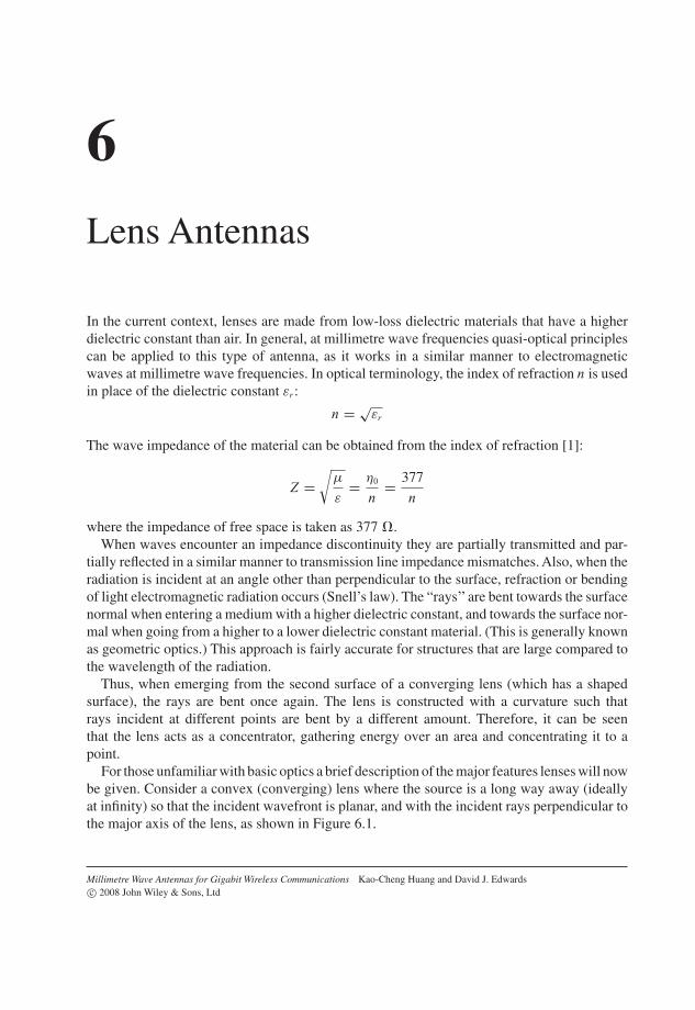
6Lens Antennas
In the current context, lenses are made from low-loss dielectric materials that have a higherdielectric constant than air. In general, at millimetre wave frequencies quasi-optical principlescan be applied to this type of antenna, as it works in a similar manner to electromagneticwaves at millimetre wave frequencies. In optical terminology, the index of refraction n is usedin place of the dielectric constant εr :
n = √εr
The wave impedance of the material can be obtained from the index of refraction [1]:
Z =√
μ
ε= η0
n= 377
n
where the impedance of free space is taken as 377 �.When waves encounter an impedance discontinuity they are partially transmitted and par-
tially reflected in a similar manner to transmission line impedance mismatches. Also, when theradiation is incident at an angle other than perpendicular to the surface, refraction or bendingof light electromagnetic radiation occurs (Snell’s law). The “rays’’are bent towards the surfacenormal when entering a medium with a higher dielectric constant, and towards the surface nor-mal when going from a higher to a lower dielectric constant material. (This is generally knownas geometric optics.) This approach is fairly accurate for structures that are large compared tothe wavelength of the radiation.
Thus, when emerging from the second surface of a converging lens (which has a shapedsurface), the rays are bent once again. The lens is constructed with a curvature such thatrays incident at different points are bent by a different amount. Therefore, it can be seenthat the lens acts as a concentrator, gathering energy over an area and concentrating it to apoint.
For those unfamiliar with basic optics a brief description of the major features lenses will nowbe given. Consider a convex (converging) lens where the source is a long way away (ideallyat infinity) so that the incident wavefront is planar, and with the incident rays perpendicular tothe major axis of the lens, as shown in Figure 6.1.
Millimetre Wave Antennas for Gigabit Wireless Communications Kao-Cheng Huang and David J. Edwardsc© 2008 John Wiley & Sons, Ltd
146 LENS ANTENNAS
Figure 6.1 A converging lens focusing light from an infinite distance. The light converges at the focallength, f , of the lens
The ray that hits the centre of the lens is exactly orthogonal to both of the lens surfaces atthis point, and therefore its direction is not changed. Rays that hit the lens at points off-centreform an angle with the local surface normal. These rays will therefore be refracted. As can beseen, the incident angle and thus the refraction angle changes with distance from the centre(axis) of the lens. Rays at the edge of the lens will be bent the most. The result is that all therays are focused at a single point behind the lens. This point is called the focal point of thelens and the distance from the lens to that point is known as the focal length. This descriptionis sufficient for thin lenses and higher-order aberration effects will not be considered at themoment.
Another interesting point is that the waves that follow each ray have exactly the same pathlength (Fermat’s principle), and therefore arrive “synchronised’’ or in phase. The rays mayhave different physical lengths, but the slower speed of light inside the lens (v = c/n) causesa delay. For example, the ray that hits the centre point of the lens is delayed the most because ittravels through the thickest part of the lens. The rays that go through the lens near the edge aredelayed the least because they travel through the thinnest part of the lens. These rays, however,travel the longest distance through air. Thus the delay through air plus the delay through thelens is always the same for rays that arrive at the focal point. Therefore, these characteristicscan be applied to the development of lens antennas.
6.1 Luneberg Lens
When a multibeam lens employs an array of primary feed elements, the high number of primaryfeed ports requires additional inputs or outputs in the beam selection switch. This of coursecauses an increase in attenuation and can result in a loss of more than 1 dB per switch.Adifferentconcept for this multibeam antenna approach was proposed by R. K. Luneberg in 1943 [2].He proposed the principle of this lens for electromagnetic waves. The general principle is thata sphere made of materials with a relative dielectric constant εr varies as the square of thedistance from the surface to the centre, and becomes a dielectric lens with foci lying on asurface:
εr = 2 − (r/R)2
where εr is relative dielectric constant, r is radius from the centre point and R is the outerradius of the lens.
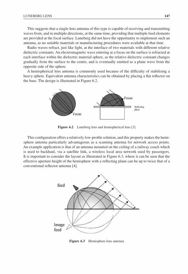
LUNEBERG LENS 147
This suggests that a single-lens antenna of this type is capable of receiving and transmittingwaves from, and in multiple directions, at the same time, providing that multiple feed elementsare provided at the focal surface. Luneberg did not have the opportunity to implement such anantenna, as no suitable materials or manufacturing procedures were available at that time.
Radio waves refract, just like light, at the interface of two materials with different relativedielectric constants. An electromagnetic wave entering at a focus on the surface is refracted ateach interface within the dielectric material sphere, as the relative dielectric constant changesgradually from the surface to the centre, and is eventually emitted as a plane wave from theopposite side of the sphere.
A hemispherical lens antenna is commonly used because of the difficulty of stabilising aheavy sphere. Equivalent antenna characteristics can be obtained by placing a flat reflector onthe base. The design is illustrated in Figure 6.2.
Figure 6.2 Luneberg lens and hemispherical lens [3]
This configuration offers a relatively low-profile solution, and this property makes the hemi-sphere antenna particularly advantageous as a scanning antenna for network access points.An example application is that of an antenna mounted on the ceiling of a railway coach whichis used to backhaul, via a satellite link, a wireless local area network used by passengers.It is important to consider the layout as illustrated in Figure 6.3, where it can be seen that theeffective aperture height of the hemisphere with a reflecting plane can be up to twice that of aconventional reflector antenna [4].
Figure 6.3 Hemisphere lens antenna
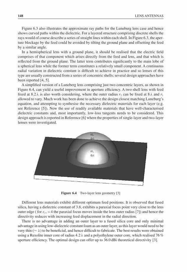
148 LENS ANTENNAS
Figure 6.3 also illustrates the approximate ray paths for the Luneburg lens case and henceshows curved paths within the dielectric. For a layered structure comprising discrete shells therays would of course describe a series of straight lines within each shell. In Figure 6.3, the aper-ture blockage by the feed could be avoided by tilting the ground plane and offsetting the feedby a similar angle.
In a hemispherical lens with a ground plane, it should be realised that the electric fieldcomprises of that component which arises directly from the feed and lens, and that which isreflected from the ground plane. The latter term contributes significantly to the main lobe ofa spherical lens while the former term constitutes a relatively small component. A continuousradial variation in dielectric constant is difficult to achieve in practice and so lenses of thistype are usually constructed from a series of concentric shells; several design approaches havebeen reported [4, 5].
A simplified version of a Luneberg lens comprising just two concentric layers, as shown inFigure 6.4, can yield a useful improvement in aperture efficiency. A two-shell lens with feedfixed at 8.2 λ is also worth considering, where the outer radius r2 can be fixed at 8 λ and r1
allowed to vary. Much work has been done to achieve the design closest matching Luneburg’sequation, and attempting to synthesise the necessary dielectric materials for each layer (e.g.see Reference [5]). Now the use of readily available materials that have well-characteriseddielectric constants and, most importantly, low-loss tangents needs to be considered. Thisdesign approach is reported in Reference [6] where the properties of single-layer and two-layerlenses were investigated.
Figure 6.4 Two-layer lens geometry [3]
Different lens materials exhibit different optimum feed positions. It is observed that fusedsilica, having a dielectric constant of 3.8, exhibits a paraxial focus point very close to the lensouter edge ( for εr1 >4 the paraxial focus moves inside the lens outer radius [7]) and hence thedirectivity reduces with increasing feed displacement in the radial direction.
There is no advantage in adding an outer layer to a fused silica core and only minimaladvantage in using low-dielectric constant foam as an outer layer, as this layer would need to bevery thin (∼ λ) to be beneficial, and hence difficult to fabricate. The best results were obtainedusing a Rexolite inner core of radius 4.2 λ and a polyethylene outer core, which realised 76 %aperture efficiency. The optimal design can offer up to 36.0 dBi theoretical directivity [3].
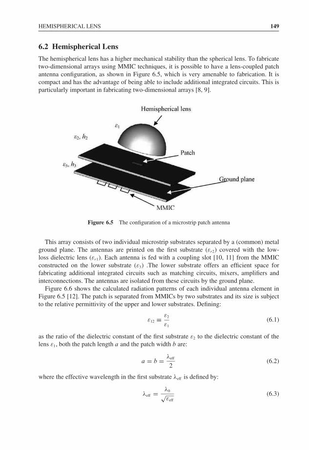
HEMISPHERICAL LENS 149
6.2 Hemispherical Lens
The hemispherical lens has a higher mechanical stability than the spherical lens. To fabricatetwo-dimensional arrays using MMIC techniques, it is possible to have a lens-coupled patchantenna configuration, as shown in Figure 6.5, which is very amenable to fabrication. It iscompact and has the advantage of being able to include additional integrated circuits. This isparticularly important in fabricating two-dimensional arrays [8, 9].
Figure 6.5 The configuration of a microstrip patch antenna
This array consists of two individual microstrip substrates separated by a (common) metalground plane. The antennas are printed on the first substrate (εr2) covered with the low-loss dielectric lens (εr1). Each antenna is fed with a coupling slot [10, 11] from the MMICconstructed on the lower substrate (ε3) .The lower substrate offers an efficient space forfabricating additional integrated circuits such as matching circuits, mixers, amplifiers andinterconnections. The antennas are isolated from these circuits by the ground plane.
Figure 6.6 shows the calculated radiation patterns of each individual antenna element inFigure 6.5 [12]. The patch is separated from MMICs by two substrates and its size is subjectto the relative permittivity of the upper and lower substrates. Defining:
ε12 ≡ ε2
ε1
(6.1)
as the ratio of the dielectric constant of the first substrate ε2 to the dielectric constant of thelens ε1, both the patch length a and the patch width b are:
a = b = λeff
2(6.2)
where the effective wavelength in the first substrate λeff is defined by:
λeff = λ0√εeff
(6.3)
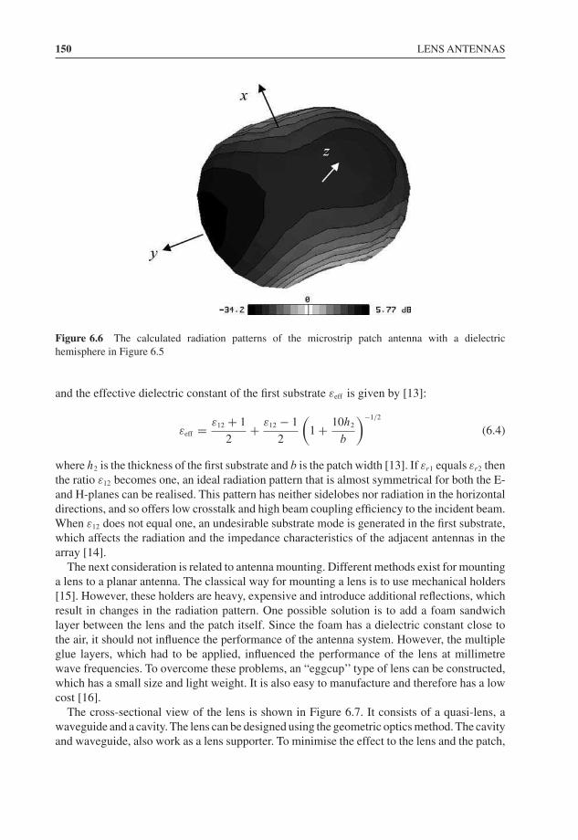
150 LENS ANTENNAS
Figure 6.6 The calculated radiation patterns of the microstrip patch antenna with a dielectrichemisphere in Figure 6.5
and the effective dielectric constant of the first substrate εeff is given by [13]:
εeff = ε12 + 1
2+ ε12 − 1
2
(1 + 10h2
b
)−1/2
(6.4)
where h2 is the thickness of the first substrate and b is the patch width [13]. If εr1 equals εr2 thenthe ratio ε12 becomes one, an ideal radiation pattern that is almost symmetrical for both the E-and H-planes can be realised. This pattern has neither sidelobes nor radiation in the horizontaldirections, and so offers low crosstalk and high beam coupling efficiency to the incident beam.When ε12 does not equal one, an undesirable substrate mode is generated in the first substrate,which affects the radiation and the impedance characteristics of the adjacent antennas in thearray [14].
The next consideration is related to antenna mounting. Different methods exist for mountinga lens to a planar antenna. The classical way for mounting a lens is to use mechanical holders[15]. However, these holders are heavy, expensive and introduce additional reflections, whichresult in changes in the radiation pattern. One possible solution is to add a foam sandwichlayer between the lens and the patch itself. Since the foam has a dielectric constant close tothe air, it should not influence the performance of the antenna system. However, the multipleglue layers, which had to be applied, influenced the performance of the lens at millimetrewave frequencies. To overcome these problems, an “eggcup’’ type of lens can be constructed,which has a small size and light weight. It is also easy to manufacture and therefore has a lowcost [16].
The cross-sectional view of the lens is shown in Figure 6.7. It consists of a quasi-lens, awaveguide and a cavity. The lens can be designed using the geometric optics method. The cavityand waveguide, also work as a lens supporter. To minimise the effect to the lens and the patch,
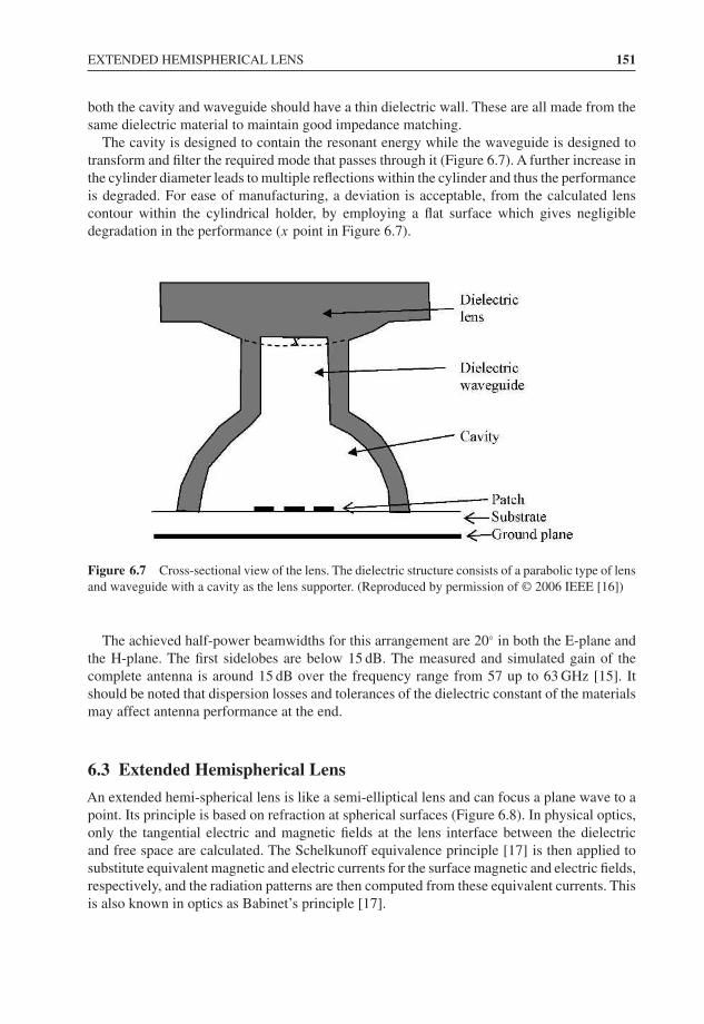
EXTENDED HEMISPHERICAL LENS 151
both the cavity and waveguide should have a thin dielectric wall. These are all made from thesame dielectric material to maintain good impedance matching.
The cavity is designed to contain the resonant energy while the waveguide is designed totransform and filter the required mode that passes through it (Figure 6.7). A further increase inthe cylinder diameter leads to multiple reflections within the cylinder and thus the performanceis degraded. For ease of manufacturing, a deviation is acceptable, from the calculated lenscontour within the cylindrical holder, by employing a flat surface which gives negligibledegradation in the performance (x point in Figure 6.7).
Figure 6.7 Cross-sectional view of the lens. The dielectric structure consists of a parabolic type of lensand waveguide with a cavity as the lens supporter. (Reproduced by permission of © 2006 IEEE [16])
The achieved half-power beamwidths for this arrangement are 20◦ in both the E-plane andthe H-plane. The first sidelobes are below 15 dB. The measured and simulated gain of thecomplete antenna is around 15 dB over the frequency range from 57 up to 63 GHz [15]. Itshould be noted that dispersion losses and tolerances of the dielectric constant of the materialsmay affect antenna performance at the end.
6.3 Extended Hemispherical Lens
An extended hemi-spherical lens is like a semi-elliptical lens and can focus a plane wave to apoint. Its principle is based on refraction at spherical surfaces (Figure 6.8). In physical optics,only the tangential electric and magnetic fields at the lens interface between the dielectricand free space are calculated. The Schelkunoff equivalence principle [17] is then applied tosubstitute equivalent magnetic and electric currents for the surface magnetic and electric fields,respectively, and the radiation patterns are then computed from these equivalent currents. Thisis also known in optics as Babinet’s principle [17].
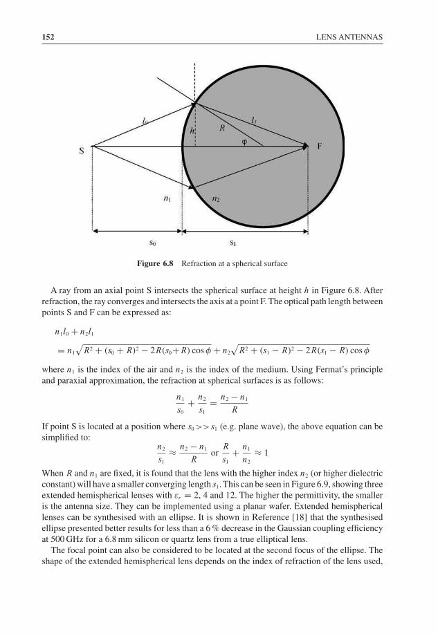
152 LENS ANTENNAS
Figure 6.8 Refraction at a spherical surface
A ray from an axial point S intersects the spherical surface at height h in Figure 6.8. Afterrefraction, the ray converges and intersects the axis at a point F. The optical path length betweenpoints S and F can be expressed as:
n1l0 + n2l1
= n1
√R2 + (s0 + R)2 − 2R(s0+R) cos φ + n2
√R2 + (s1 − R)2 − 2R(s1 − R) cos φ
where n1 is the index of the air and n2 is the index of the medium. Using Fermat’s principleand paraxial approximation, the refraction at spherical surfaces is as follows:
n1
s0
+ n2
s1
= n2 − n1
R
If point S is located at a position where s0 >>s1 (e.g. plane wave), the above equation can besimplified to:
n2
s1
≈ n2 − n1
Ror
R
s1
+ n1
n2
≈ 1
When R and n1 are fixed, it is found that the lens with the higher index n2 (or higher dielectricconstant) will have a smaller converging length s1. This can be seen in Figure 6.9, showing threeextended hemispherical lenses with εr = 2, 4 and 12. The higher the permittivity, the smalleris the antenna size. They can be implemented using a planar wafer. Extended hemisphericallenses can be synthesised with an ellipse. It is shown in Reference [18] that the synthesisedellipse presented better results for less than a 6 % decrease in the Gaussian coupling efficiencyat 500 GHz for a 6.8 mm silicon or quartz lens from a true elliptical lens.
The focal point can also be considered to be located at the second focus of the ellipse. Theshape of the extended hemispherical lens depends on the index of refraction of the lens used,
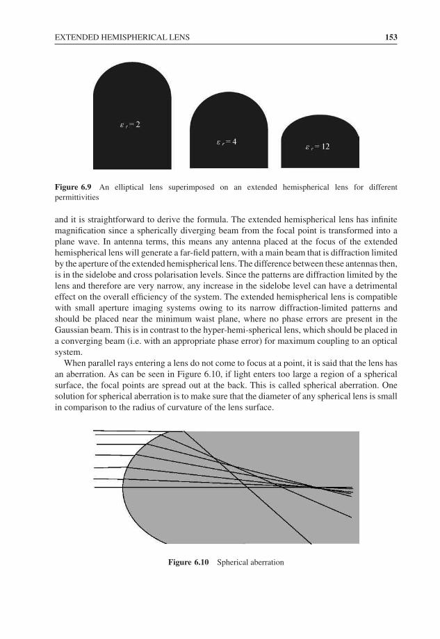
EXTENDED HEMISPHERICAL LENS 153
Figure 6.9 An elliptical lens superimposed on an extended hemispherical lens for differentpermittivities
and it is straightforward to derive the formula. The extended hemispherical lens has infinitemagnification since a spherically diverging beam from the focal point is transformed into aplane wave. In antenna terms, this means any antenna placed at the focus of the extendedhemispherical lens will generate a far-field pattern, with a main beam that is diffraction limitedby the aperture of the extended hemispherical lens. The difference between these antennas then,is in the sidelobe and cross polarisation levels. Since the patterns are diffraction limited by thelens and therefore are very narrow, any increase in the sidelobe level can have a detrimentaleffect on the overall efficiency of the system. The extended hemispherical lens is compatiblewith small aperture imaging systems owing to its narrow diffraction-limited patterns andshould be placed near the minimum waist plane, where no phase errors are present in theGaussian beam. This is in contrast to the hyper-hemi-spherical lens, which should be placed ina converging beam (i.e. with an appropriate phase error) for maximum coupling to an opticalsystem.
When parallel rays entering a lens do not come to focus at a point, it is said that the lens hasan aberration. As can be seen in Figure 6.10, if light enters too large a region of a sphericalsurface, the focal points are spread out at the back. This is called spherical aberration. Onesolution for spherical aberration is to make sure that the diameter of any spherical lens is smallin comparison to the radius of curvature of the lens surface.
Figure 6.10 Spherical aberration
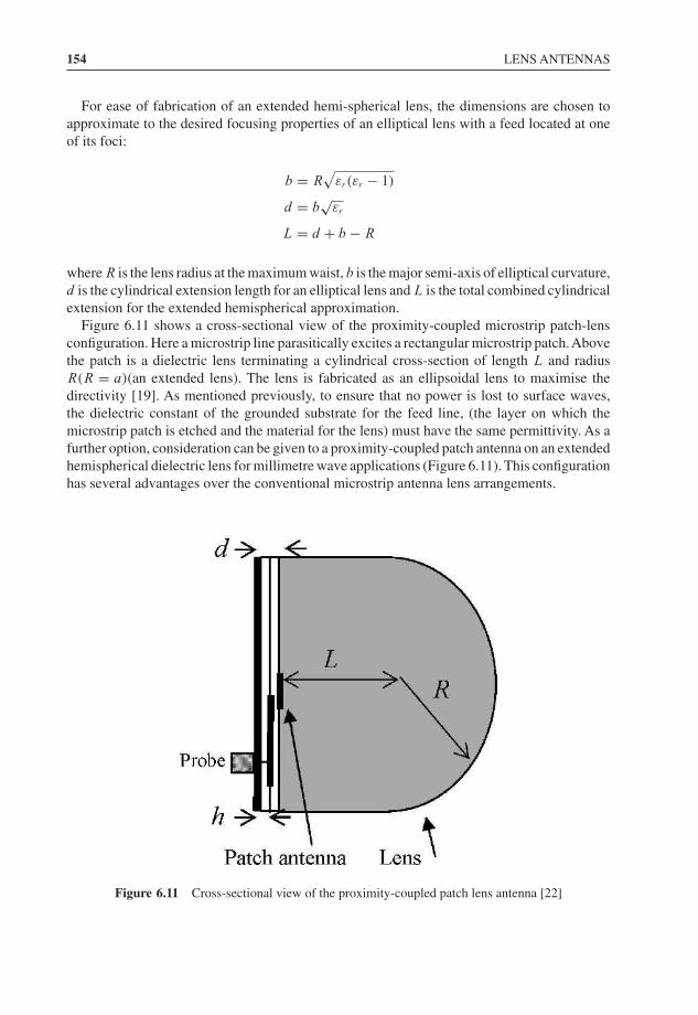
154 LENS ANTENNAS
For ease of fabrication of an extended hemi-spherical lens, the dimensions are chosen toapproximate to the desired focusing properties of an elliptical lens with a feed located at oneof its foci:
b = R√
εr(εr − 1)
d = b√
εr
L = d + b − R
where R is the lens radius at the maximum waist, b is the major semi-axis of elliptical curvature,d is the cylindrical extension length for an elliptical lens and L is the total combined cylindricalextension for the extended hemispherical approximation.
Figure 6.11 shows a cross-sectional view of the proximity-coupled microstrip patch-lensconfiguration. Here a microstrip line parasitically excites a rectangular microstrip patch.Abovethe patch is a dielectric lens terminating a cylindrical cross-section of length L and radiusR(R = a)(an extended lens). The lens is fabricated as an ellipsoidal lens to maximise thedirectivity [19]. As mentioned previously, to ensure that no power is lost to surface waves,the dielectric constant of the grounded substrate for the feed line, (the layer on which themicrostrip patch is etched and the material for the lens) must have the same permittivity. As afurther option, consideration can be given to a proximity-coupled patch antenna on an extendedhemispherical dielectric lens for millimetre wave applications (Figure 6.11). This configurationhas several advantages over the conventional microstrip antenna lens arrangements.
Figure 6.11 Cross-sectional view of the proximity-coupled patch lens antenna [22]
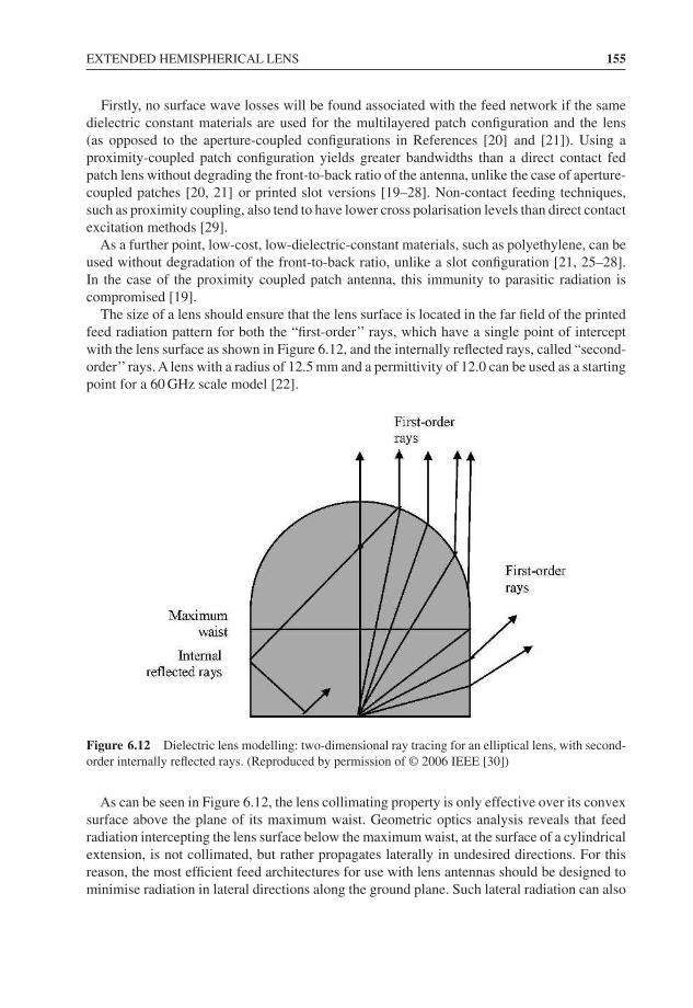
EXTENDED HEMISPHERICAL LENS 155
Firstly, no surface wave losses will be found associated with the feed network if the samedielectric constant materials are used for the multilayered patch configuration and the lens(as opposed to the aperture-coupled configurations in References [20] and [21]). Using aproximity-coupled patch configuration yields greater bandwidths than a direct contact fedpatch lens without degrading the front-to-back ratio of the antenna, unlike the case of aperture-coupled patches [20, 21] or printed slot versions [19–28]. Non-contact feeding techniques,such as proximity coupling, also tend to have lower cross polarisation levels than direct contactexcitation methods [29].
As a further point, low-cost, low-dielectric-constant materials, such as polyethylene, can beused without degradation of the front-to-back ratio, unlike a slot configuration [21, 25–28].In the case of the proximity coupled patch antenna, this immunity to parasitic radiation iscompromised [19].
The size of a lens should ensure that the lens surface is located in the far field of the printedfeed radiation pattern for both the “first-order’’ rays, which have a single point of interceptwith the lens surface as shown in Figure 6.12, and the internally reflected rays, called “second-order’’ rays. A lens with a radius of 12.5 mm and a permittivity of 12.0 can be used as a startingpoint for a 60 GHz scale model [22].
Figure 6.12 Dielectric lens modelling: two-dimensional ray tracing for an elliptical lens, with second-order internally reflected rays. (Reproduced by permission of © 2006 IEEE [30])
As can be seen in Figure 6.12, the lens collimating property is only effective over its convexsurface above the plane of its maximum waist. Geometric optics analysis reveals that feedradiation intercepting the lens surface below the maximum waist, at the surface of a cylindricalextension, is not collimated, but rather propagates laterally in undesired directions. For thisreason, the most efficient feed architectures for use with lens antennas should be designed tominimise radiation in lateral directions along the ground plane. Such lateral radiation can also
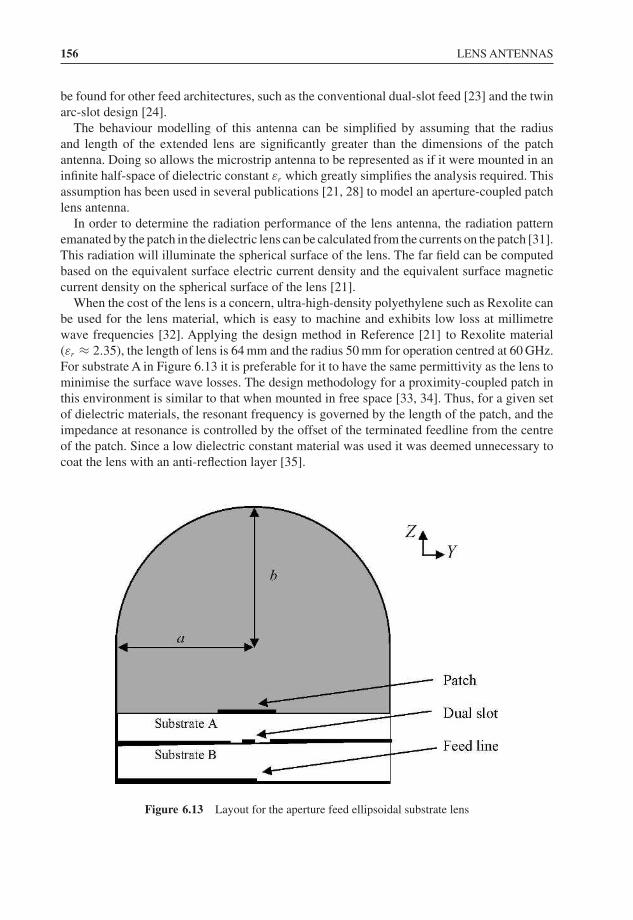
156 LENS ANTENNAS
be found for other feed architectures, such as the conventional dual-slot feed [23] and the twinarc-slot design [24].
The behaviour modelling of this antenna can be simplified by assuming that the radiusand length of the extended lens are significantly greater than the dimensions of the patchantenna. Doing so allows the microstrip antenna to be represented as if it were mounted in aninfinite half-space of dielectric constant εr which greatly simplifies the analysis required. Thisassumption has been used in several publications [21, 28] to model an aperture-coupled patchlens antenna.
In order to determine the radiation performance of the lens antenna, the radiation patternemanated by the patch in the dielectric lens can be calculated from the currents on the patch [31].This radiation will illuminate the spherical surface of the lens. The far field can be computedbased on the equivalent surface electric current density and the equivalent surface magneticcurrent density on the spherical surface of the lens [21].
When the cost of the lens is a concern, ultra-high-density polyethylene such as Rexolite canbe used for the lens material, which is easy to machine and exhibits low loss at millimetrewave frequencies [32]. Applying the design method in Reference [21] to Rexolite material(εr ≈ 2.35), the length of lens is 64 mm and the radius 50 mm for operation centred at 60 GHz.For substrate A in Figure 6.13 it is preferable for it to have the same permittivity as the lens tominimise the surface wave losses. The design methodology for a proximity-coupled patch inthis environment is similar to that when mounted in free space [33, 34]. Thus, for a given setof dielectric materials, the resonant frequency is governed by the length of the patch, and theimpedance at resonance is controlled by the offset of the terminated feedline from the centreof the patch. Since a low dielectric constant material was used it was deemed unnecessary tocoat the lens with an anti-reflection layer [35].
Figure 6.13 Layout for the aperture feed ellipsoidal substrate lens
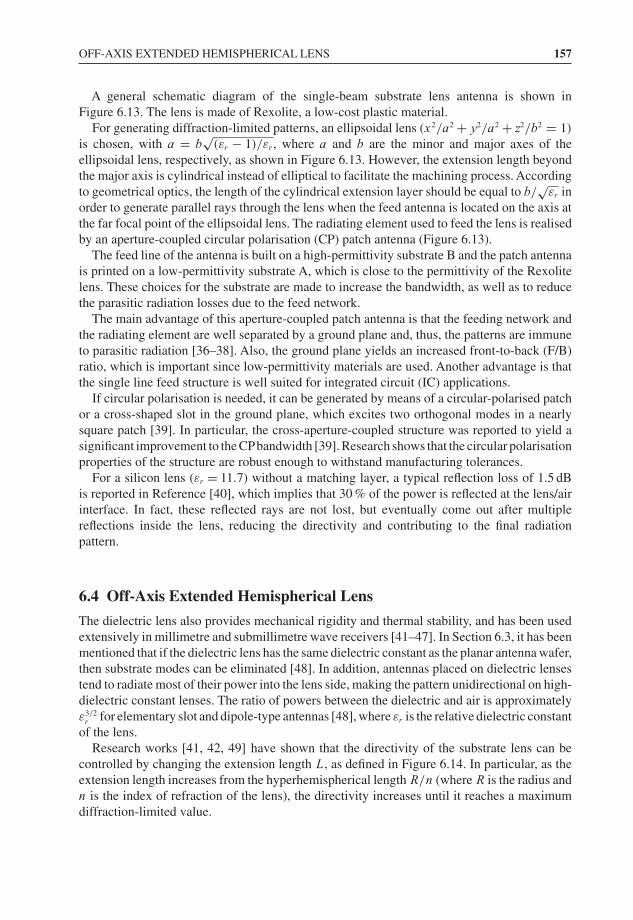
OFF-AXIS EXTENDED HEMISPHERICAL LENS 157
A general schematic diagram of the single-beam substrate lens antenna is shown inFigure 6.13. The lens is made of Rexolite, a low-cost plastic material.
For generating diffraction-limited patterns, an ellipsoidal lens (x2/a2 + y2/a2 + z2/b2 = 1)is chosen, with a = b
√(εr − 1)/εr , where a and b are the minor and major axes of the
ellipsoidal lens, respectively, as shown in Figure 6.13. However, the extension length beyondthe major axis is cylindrical instead of elliptical to facilitate the machining process. Accordingto geometrical optics, the length of the cylindrical extension layer should be equal to b/
√εr in
order to generate parallel rays through the lens when the feed antenna is located on the axis atthe far focal point of the ellipsoidal lens. The radiating element used to feed the lens is realisedby an aperture-coupled circular polarisation (CP) patch antenna (Figure 6.13).
The feed line of the antenna is built on a high-permittivity substrate B and the patch antennais printed on a low-permittivity substrate A, which is close to the permittivity of the Rexolitelens. These choices for the substrate are made to increase the bandwidth, as well as to reducethe parasitic radiation losses due to the feed network.
The main advantage of this aperture-coupled patch antenna is that the feeding network andthe radiating element are well separated by a ground plane and, thus, the patterns are immuneto parasitic radiation [36–38]. Also, the ground plane yields an increased front-to-back (F/B)ratio, which is important since low-permittivity materials are used. Another advantage is thatthe single line feed structure is well suited for integrated circuit (IC) applications.
If circular polarisation is needed, it can be generated by means of a circular-polarised patchor a cross-shaped slot in the ground plane, which excites two orthogonal modes in a nearlysquare patch [39]. In particular, the cross-aperture-coupled structure was reported to yield asignificant improvement to the CPbandwidth [39]. Research shows that the circular polarisationproperties of the structure are robust enough to withstand manufacturing tolerances.
For a silicon lens (εr = 11.7) without a matching layer, a typical reflection loss of 1.5 dBis reported in Reference [40], which implies that 30 % of the power is reflected at the lens/airinterface. In fact, these reflected rays are not lost, but eventually come out after multiplereflections inside the lens, reducing the directivity and contributing to the final radiationpattern.
6.4 Off-Axis Extended Hemispherical Lens
The dielectric lens also provides mechanical rigidity and thermal stability, and has been usedextensively in millimetre and submillimetre wave receivers [41–47]. In Section 6.3, it has beenmentioned that if the dielectric lens has the same dielectric constant as the planar antenna wafer,then substrate modes can be eliminated [48]. In addition, antennas placed on dielectric lensestend to radiate most of their power into the lens side, making the pattern unidirectional on high-dielectric constant lenses. The ratio of powers between the dielectric and air is approximatelyε3/2
rfor elementary slot and dipole-type antennas [48], where εr is the relative dielectric constant
of the lens.Research works [41, 42, 49] have shown that the directivity of the substrate lens can be
controlled by changing the extension length L, as defined in Figure 6.14. In particular, as theextension length increases from the hyperhemispherical length R/n (where R is the radius andn is the index of refraction of the lens), the directivity increases until it reaches a maximumdiffraction-limited value.
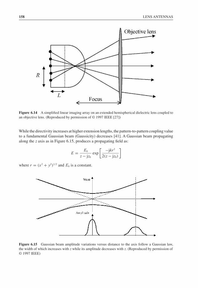
158 LENS ANTENNAS
Figure 6.14 A simplified linear imaging array on an extended hemispherical dielectric lens coupled toan objective lens. (Reproduced by permission of © 1997 IEEE [27])
While the directivity increases at higher extension lengths, the pattern-to-pattern coupling valueto a fundamental Gaussian beam (Gaussicity) decreases [41]. A Gaussian beam propagatingalong the z axis as in Figure 6.15, produces a propagating field as:
E = E0
z − jz0
exp
[ −jkr2
2(z − jz0)
]
where r = (x2 + y2)1/2 and E0 is a constant.
Figure 6.15 Gaussian beam amplitude variations versus distance to the axis follow a Gaussian law,the width of which increases with z while its amplitude decreases with z. (Reproduced by permission of© 1997 IEEE)
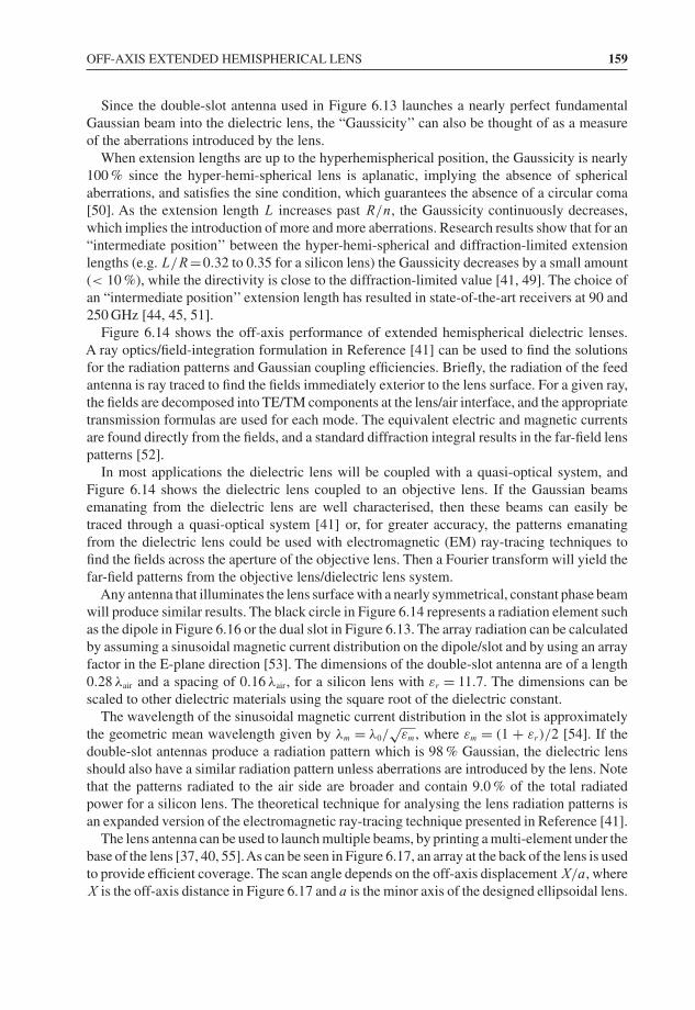
OFF-AXIS EXTENDED HEMISPHERICAL LENS 159
Since the double-slot antenna used in Figure 6.13 launches a nearly perfect fundamentalGaussian beam into the dielectric lens, the “Gaussicity’’ can also be thought of as a measureof the aberrations introduced by the lens.
When extension lengths are up to the hyperhemispherical position, the Gaussicity is nearly100 % since the hyper-hemi-spherical lens is aplanatic, implying the absence of sphericalaberrations, and satisfies the sine condition, which guarantees the absence of a circular coma[50]. As the extension length L increases past R/n, the Gaussicity continuously decreases,which implies the introduction of more and more aberrations. Research results show that for an“intermediate position’’ between the hyper-hemi-spherical and diffraction-limited extensionlengths (e.g. L/R=0.32 to 0.35 for a silicon lens) the Gaussicity decreases by a small amount(< 10 %), while the directivity is close to the diffraction-limited value [41, 49]. The choice ofan “intermediate position’’ extension length has resulted in state-of-the-art receivers at 90 and250 GHz [44, 45, 51].
Figure 6.14 shows the off-axis performance of extended hemispherical dielectric lenses.A ray optics/field-integration formulation in Reference [41] can be used to find the solutionsfor the radiation patterns and Gaussian coupling efficiencies. Briefly, the radiation of the feedantenna is ray traced to find the fields immediately exterior to the lens surface. For a given ray,the fields are decomposed into TE/TM components at the lens/air interface, and the appropriatetransmission formulas are used for each mode. The equivalent electric and magnetic currentsare found directly from the fields, and a standard diffraction integral results in the far-field lenspatterns [52].
In most applications the dielectric lens will be coupled with a quasi-optical system, andFigure 6.14 shows the dielectric lens coupled to an objective lens. If the Gaussian beamsemanating from the dielectric lens are well characterised, then these beams can easily betraced through a quasi-optical system [41] or, for greater accuracy, the patterns emanatingfrom the dielectric lens could be used with electromagnetic (EM) ray-tracing techniques tofind the fields across the aperture of the objective lens. Then a Fourier transform will yield thefar-field patterns from the objective lens/dielectric lens system.
Any antenna that illuminates the lens surface with a nearly symmetrical, constant phase beamwill produce similar results. The black circle in Figure 6.14 represents a radiation element suchas the dipole in Figure 6.16 or the dual slot in Figure 6.13. The array radiation can be calculatedby assuming a sinusoidal magnetic current distribution on the dipole/slot and by using an arrayfactor in the E-plane direction [53]. The dimensions of the double-slot antenna are of a length0.28 λair and a spacing of 0.16 λair , for a silicon lens with εr = 11.7. The dimensions can bescaled to other dielectric materials using the square root of the dielectric constant.
The wavelength of the sinusoidal magnetic current distribution in the slot is approximatelythe geometric mean wavelength given by λm = λ0/
√εm, where εm = (1 + εr)/2 [54]. If the
double-slot antennas produce a radiation pattern which is 98 % Gaussian, the dielectric lensshould also have a similar radiation pattern unless aberrations are introduced by the lens. Notethat the patterns radiated to the air side are broader and contain 9.0 % of the total radiatedpower for a silicon lens. The theoretical technique for analysing the lens radiation patterns isan expanded version of the electromagnetic ray-tracing technique presented in Reference [41].
The lens antenna can be used to launch multiple beams, by printing a multi-element under thebase of the lens [37, 40, 55].As can be seen in Figure 6.17, an array at the back of the lens is usedto provide efficient coverage. The scan angle depends on the off-axis displacement X/a, whereX is the off-axis distance in Figure 6.17 and a is the minor axis of the designed ellipsoidal lens.
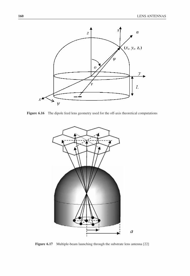
160 LENS ANTENNAS
Figure 6.16 The dipole feed lens geometry used for the off-axis theoretical computations
Figure 6.17 Multiple-beam launching through the substrate lens antenna [22]
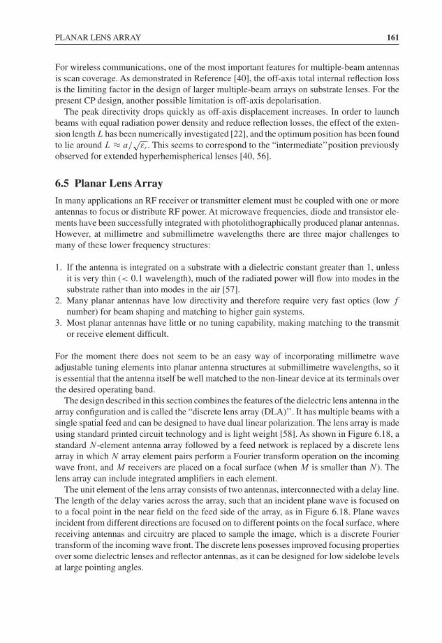
PLANAR LENS ARRAY 161
For wireless communications, one of the most important features for multiple-beam antennasis scan coverage. As demonstrated in Reference [40], the off-axis total internal reflection lossis the limiting factor in the design of larger multiple-beam arrays on substrate lenses. For thepresent CP design, another possible limitation is off-axis depolarisation.
The peak directivity drops quickly as off-axis displacement increases. In order to launchbeams with equal radiation power density and reduce reflection losses, the effect of the exten-sion length L has been numerically investigated [22], and the optimum position has been foundto lie around L ≈ a/
√εr . This seems to correspond to the “intermediate’’position previously
observed for extended hyperhemispherical lenses [40, 56].
6.5 Planar Lens Array
In many applications an RF receiver or transmitter element must be coupled with one or moreantennas to focus or distribute RF power. At microwave frequencies, diode and transistor ele-ments have been successfully integrated with photolithographically produced planar antennas.However, at millimetre and submillimetre wavelengths there are three major challenges tomany of these lower frequency structures:
1. If the antenna is integrated on a substrate with a dielectric constant greater than 1, unlessit is very thin (< 0.1 wavelength), much of the radiated power will flow into modes in thesubstrate rather than into modes in the air [57].
2. Many planar antennas have low directivity and therefore require very fast optics (low f
number) for beam shaping and matching to higher gain systems.3. Most planar antennas have little or no tuning capability, making matching to the transmit
or receive element difficult.
For the moment there does not seem to be an easy way of incorporating millimetre waveadjustable tuning elements into planar antenna structures at submillimetre wavelengths, so itis essential that the antenna itself be well matched to the non-linear device at its terminals overthe desired operating band.
The design described in this section combines the features of the dielectric lens antenna in thearray configuration and is called the “discrete lens array (DLA)’’. It has multiple beams with asingle spatial feed and can be designed to have dual linear polarization. The lens array is madeusing standard printed circuit technology and is light weight [58]. As shown in Figure 6.18, astandard N -element antenna array followed by a feed network is replaced by a discrete lensarray in which N array element pairs perform a Fourier transform operation on the incomingwave front, and M receivers are placed on a focal surface (when M is smaller than N ). Thelens array can include integrated amplifiers in each element.
The unit element of the lens array consists of two antennas, interconnected with a delay line.The length of the delay varies across the array, such that an incident plane wave is focused onto a focal point in the near field on the feed side of the array, as in Figure 6.18. Plane wavesincident from different directions are focused on to different points on the focal surface, wherereceiving antennas and circuitry are placed to sample the image, which is a discrete Fouriertransform of the incoming wave front. The discrete lens posesses improved focusing propertiesover some dielectric lenses and reflector antennas, as it can be designed for low sidelobe levelsat large pointing angles.
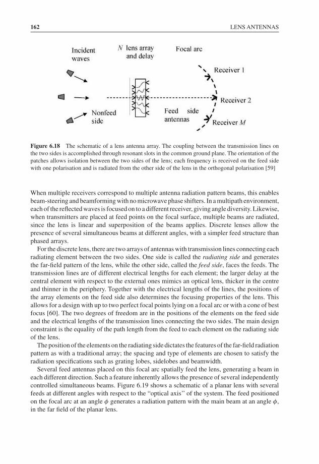
162 LENS ANTENNAS
Figure 6.18 The schematic of a lens antenna array. The coupling between the transmission lines onthe two sides is accomplished through resonant slots in the common ground plane. The orientation of thepatches allows isolation between the two sides of the lens; each frequency is received on the feed sidewith one polarisation and is radiated from the other side of the lens in the orthogonal polarisation [59]
When multiple receivers correspond to multiple antenna radiation pattern beams, this enablesbeam-steering and beamforming with no microwave phase shifters. In a multipath environment,each of the reflected waves is focused on to a different receiver, giving angle diversity. Likewise,when transmitters are placed at feed points on the focal surface, multiple beams are radiated,since the lens is linear and superposition of the beams applies. Discrete lenses allow thepresence of several simultaneous beams at different angles, with a simpler feed structure thanphased arrays.
For the discrete lens, there are two arrays of antennas with transmission lines connecting eachradiating element between the two sides. One side is called the radiating side and generatesthe far-field pattern of the lens, while the other side, called the feed side, faces the feeds. Thetransmission lines are of different electrical lengths for each element; the larger delay at thecentral element with respect to the external ones mimics an optical lens, thicker in the centreand thinner in the periphery. Together with the electrical lengths of the lines, the positions ofthe array elements on the feed side also determines the focusing properties of the lens. Thisallows for a design with up to two perfect focal points lying on a focal arc or with a cone of bestfocus [60]. The two degrees of freedom are in the positions of the elements on the feed sideand the electrical lengths of the transmission lines connecting the two sides. The main designconstraint is the equality of the path length from the feed to each element on the radiating sideof the lens.
The position of the elements on the radiating side dictates the features of the far-field radiationpattern as with a traditional array; the spacing and type of elements are chosen to satisfy theradiation specifications such as grating lobes, sidelobes and beamwidth.
Several feed antennas placed on this focal arc spatially feed the lens, generating a beam ineach different direction. Such a feature inherently allows the presence of several independentlycontrolled simultaneous beams. Figure 6.19 shows a schematic of a planar lens with severalfeeds at different angles with respect to the “optical axis’’ of the system. The feed positionedon the focal arc at an angle φ generates a radiation pattern with the main beam at an angle φ,in the far field of the planar lens.
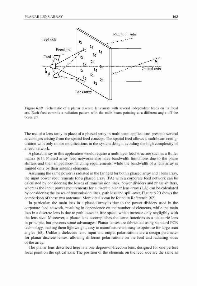
PLANAR LENS ARRAY 163
Figure 6.19 Schematic of a planar discrete lens array with several independent feeds on its focalarc. Each feed controls a radiation pattern with the main beam pointing at a different angle off theboresight
The use of a lens array in place of a phased array in multibeam applications presents severaladvantages arising from the spatial feed concept. The spatial feed allows a multibeam config-uration with only minor modifications in the system design, avoiding the high complexity ofa feed network.
A phased array in this application would require a multilayer feed structure such as a Butlermatrix [61]. Phased array feed networks also have bandwidth limitations due to the phaseshifters and their impedance-matching requirements, while the bandwidth of a lens array islimited only by their antenna elements.
Assuming the same power is radiated in the far field for both a phased array and a lens array,the input power requirements for a phased array (PA) with a corporate feed network can becalculated by considering the losses of transmission lines, power dividers and phase shifters,whereas the input power requirements for a discrete planar lens array (LA) can be calculatedby considering the losses of transmission lines, path loss and spill-over. Figure 6.20 shows thecomparison of these two antennas. More details can be found in Reference [62].
In particular, the main loss in a phased array is due to the power dividers used in thecorporate feed network, resulting in dependence on the number of elements, while the mainloss in a discrete lens is due to path losses in free space, which increase only negligibly withthe lens size. Moreover, a planar lens accomplishes the same functions as a dielectric lensin principle, but presents some advantages. Planar lenses are fabricated using standard PCBtechnology, making them lightweight, easy to manufacture and easy to optimise for large scanangles [63]. Unlike a dielectric lens, input and output polarisations are a design parameterfor planar discrete lenses, allowing different polarisations on the feed and radiating sidesof the array.
The planar lens described here is a one degree-of-freedom lens, designed for one perfectfocal point on the optical axis. The position of the elements on the feed side are the same as
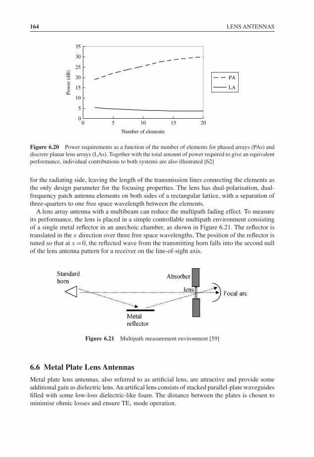
164 LENS ANTENNAS
0
5
10
15
20
25
30
35
0 5 10 15 20
Number of elements
Pow
er (
dB)
PA
LA
Figure 6.20 Power requirements as a function of the number of elements for phased arrays (PAs) anddiscrete planar lens arrays (LAs). Together with the total amount of power required to give an equivalentperformance, individual contributions to both systems are also illustrated [62]
for the radiating side, leaving the length of the transmission lines connecting the elements asthe only design parameter for the focusing properties. The lens has dual-polarisation, dual-frequency patch antenna elements on both sides of a rectangular lattice, with a separation ofthree-quarters to one free space wavelength between the elements.
A lens array antenna with a multibeam can reduce the multipath fading effect. To measureits performance, the lens is placed in a simple controllable multipath environment consistingof a single metal reflector in an anechoic chamber, as shown in Figure 6.21. The reflector istranslated in the x direction over three free space wavelengths. The position of the reflector istuned so that at x =0, the reflected wave from the transmitting horn falls into the second nullof the lens antenna pattern for a receiver on the line-of-sight axis.
Figure 6.21 Multipath measurement environment [59]
6.6 Metal Plate Lens Antennas
Metal plate lens antennas, also referred to as artificial lens, are attractive and provide someadditional gain as dielectric lens. An artifical lens consists of stacked parallel-plate waveguidesfilled with some low-loss dielectric-like foam. The distance between the plates is chosen tominimise ohmic losses and ensure TE1 mode operation.
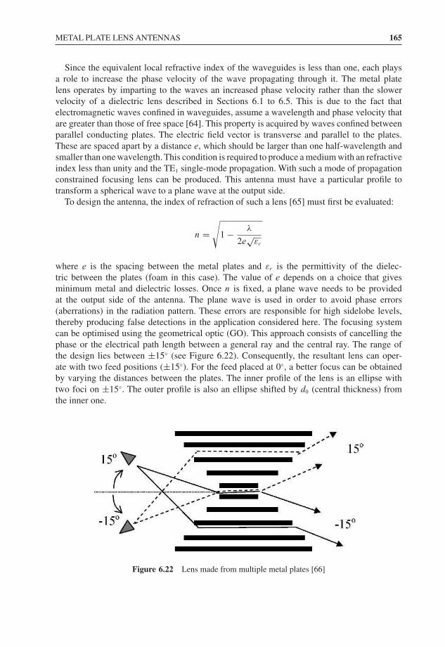
METAL PLATE LENS ANTENNAS 165
Since the equivalent local refractive index of the waveguides is less than one, each playsa role to increase the phase velocity of the wave propagating through it. The metal platelens operates by imparting to the waves an increased phase velocity rather than the slowervelocity of a dielectric lens described in Sections 6.1 to 6.5. This is due to the fact thatelectromagnetic waves confined in waveguides, assume a wavelength and phase velocity thatare greater than those of free space [64]. This property is acquired by waves confined betweenparallel conducting plates. The electric field vector is transverse and parallel to the plates.These are spaced apart by a distance e, which should be larger than one half-wavelength andsmaller than one wavelength. This condition is required to produce a medium with an refractiveindex less than unity and the TE1 single-mode propagation. With such a mode of propagationconstrained focusing lens can be produced. This antenna must have a particular profile totransform a spherical wave to a plane wave at the output side.
To design the antenna, the index of refraction of such a lens [65] must first be evaluated:
n =√
1 − λ
2e√
εr
where e is the spacing between the metal plates and εr is the permittivity of the dielec-tric between the plates (foam in this case). The value of e depends on a choice that givesminimum metal and dielectric losses. Once n is fixed, a plane wave needs to be providedat the output side of the antenna. The plane wave is used in order to avoid phase errors(aberrations) in the radiation pattern. These errors are responsible for high sidelobe levels,thereby producing false detections in the application considered here. The focusing systemcan be optimised using the geometrical optic (GO). This approach consists of cancelling thephase or the electrical path length between a general ray and the central ray. The range ofthe design lies between ±15◦ (see Figure 6.22). Consequently, the resultant lens can oper-ate with two feed positions (±15◦). For the feed placed at 0◦, a better focus can be obtainedby varying the distances between the plates. The inner profile of the lens is an ellipse withtwo foci on ±15◦. The outer profile is also an ellipse shifted by d0 (central thickness) fromthe inner one.
Figure 6.22 Lens made from multiple metal plates [66]
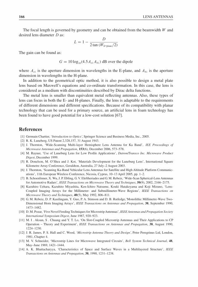
166 LENS ANTENNAS
The focal length is governed by geometry and can be obtained from the beamwidth W anddesired lens diameter D as:
L = 1 − D
2 tan (WE-plane/2)
The gain can be found as:
G = 10 log10(4.5AeλAhλ) dB over the dipole
where Aeλ is the aperture dimension in wavelengths in the E-plane, and Ahλ is the aperturedimension in wavelengths in the H-plane.
In addition to the geometrical optic method, it is also possible to design a metal platelens based on Maxwell’s equations and co-ordinate transformation. In this case, the lens isconsidered as a medium with discontinuities described by Dirac delta functions.
The metal lens is smaller than equivalent metal reflecting antennas. Also, these types oflens can focus in both the E- and H-planes. Finally, the lens is adaptable to the requirementsof different dimensions and different specifications. Because of its compatibility with planartechnology that can be used for a primary source, an artificial lens in foam technology hasbeen found to have good potential for a low-cost solution [67].
References[1] Germain Chartier, ‘Introduction to Optics’, Springer Science and Business Media, Inc., 2005.[2] R. K. Luneberg, US Patent 2,328,157, 31 August 1943.[3] J. Thornton, ‘Wide-Scanning Multi-layer Hemisphere Lens Antenna for Ka Band’, IEE Proceedings of
Microwave Antennas and Propagation, 153(6), December 2006, 573–578.[4] M. Rayner, ‘Use of Luneburg Lens for Low Profile Applications’, Datron/Transco Inc. Microwave Product
Digest, December 1999.[5] R. Donelson, M. O’Shea and J. Kot, ‘Materials Development for the Luneburg Lens’, International Square
Kilometre Array Conference, Geraldton, Australia, 27 July–2 August 2003.[6] J. Thornton, ‘Scanning Ka-Band Vehicular Lens Antennas for Satellite and High Altitude Platform Communic-
ations’, 11th European Wireless Conference, Nicosia, Cyprus, 10–13 April 2005, pp. 1–2.[7] B. Schoenlinner, X. Wu, J. P. Ebling, G. V. Eleftheriades and G. M. Rebeiz, ‘Wide-Scan Spherical-Lens Antennas
for Automotive Radars’, IEEE Transactions on Microwave Theory and Techniques, 50(9), 2002, 2166–2175.[8] Kazuhiro Uehara, Kazuhito Miyashita, Ken-Ichiro Natsume, Kouki Hatakeyama and Koji Mizuno, ‘Lens-
Coupled Imaging Arrays for the Millimeter- and Submillimeter-Wave Regions’, IEEE Transactions onMicrowave Theory and Techniques, 40(5), May 1992, 806–811.
[9] G. M. Rebeiz, D. P. Kasilingam, Y. Guo, P. A. Stimson and D. B. Rutledge,‘Monolithic Millimetre-Wave Two-Dimensional Horn Imaging Arrays’, IEEE Transactions on Antennas and Propagation, 38, September 1990,1473–1482.
[10] D. M. Pozar, ‘Five Novel Feeding Techniques for MicrostripAntennas’, IEEE Antennas and Propagation SocietyInternational Symposium Digest, June 1987, 920–923.
[11] M. I . Aksun, S . Chuang and Y. T. Lo, ‘On Slot-Coupled Microstrip Antennas and Their Applications to CPOperation – Theory and Experiment’, IEEE Transactions on Antennas and Propagation, 38, August 1990,1224–1230.
[12] J. R. James, P. S. Hall and C. Wood, ‘Microstrip Antenna Theory and Design’, Peter Peregrinus Ltd, London,1981, Chapter 4.
[13] M. V. Schneider, ‘Microstrip Lines for Microwave Integrated Circuits’, Bell System Technical Journal, 48,May–June 1969, 1421–1444.
[14] A. K. Bhattacharyya, ‘Characteristics of Space and Surface Waves in a Multilayered Structure’, IEEETransactions on Antennas and Propagation, 38, 1990, 1231–1238.

REFERENCES 167
[15] U. Sangawa, K. Takahashi, T. Urabe, H. Ogura and H. Yabuki, ‘A Ka-Band High-Efficiency Dielectric LensAntenna with a Silicon Micromachined Microstrip Patch Radiator’, IEEE MTT-S International Digest, 1, May2001, 389–392.
[16] M. Al-Tikriti, S. Koch and M. Uno, ‘A Compact Broadband Stacked Microstrip Array Antenna Using Eggcup-Type of Lens, IEEE Microwave and Wireless Components Letters, 16(4), April 2006, 230–232.
[17] Wikipedia, http://www.wikipedia.org/[18] D. F. Filipovic, S. S. Gearhart and G. M. Rebeiz, ‘Double-SlotAntennas on Extended Hemispherical and Elliptical
Dielectric Lenses’, IEEE Transactions on Microwave Theory and Techniques, October 1993.[19] D. F. Filipovic, S. G. Gearhart and G. M. Rebeiz, ‘Double-Slot Antennas on Extended Hemispherical and Ellipt-
ical Silicon Dielectric Lenses’, IEEE Transactions on Microwave Theory and Techniques, 41, October 1993,1738–1749.
[20] G. V. Eleftheriades, Y. Brand, J.-F. Zurcher and J. R. Mosig, ‘ALPSS: A Millimetre-Wave Aperture-CoupledPatch Antenna on a Substrate Lens’, Electronics Letters, 33, January 1997, 169–170.
[21] X. Wu, G. V. Eleftheriades and E. Van Deventer, ‘Design and Characterization of Single and Multiple Beam mm-Wave Circularly Polarized Lens Antennas for Wireless Communications’, IEEE AP-S International Antennasand Propagation Symposium, Orlando, Florida, July 1999, pp. 1200–1204.
[22] X. Wu, G. V. Eleftheriades and T. E. van Deventer-Perkins, ‘Design and Characterization of Single- andMultiple-Beam mm-Wave Circularly Polarized Substrate Lens Antennas for Wireless Communications’, IEEETransactions on Microwave Theory and Techniques, 49(3), March 2001, 431–441.
[23] D. F. Filipovic, S. S. Gearhart and G. M. Rebeiz, ‘Double-Slot Antennas on Extended Hemispherical andElliptical Silicon Dielectric Lenses’, IEEE Transactions on Microwave Theory and Techniques, 41(10), October1993, 1738–1749.
[24] M. Qiu and G. V. Eleftheriades, ‘Highly Efficient Unidirectional Twin Arc-Slot Antennas on Electrically ThinSubstrates’, IEEE Transactions on Antennas and Propagation, 52(1), January 2004, 53–58.
[25] D. F. Filipovic and G. M. Rebeiz, ‘Double-Slot Antennas on Extended Hemispherical and Elliptical QuartzDielectric Lenses’, International Journal of Infrared Millimetre Waves, 14, 1993, 1905–1924.
[26] J. Zmuidzinas and H. G. LeDuc, ‘Quasioptical Slot Antenna SIS Mixers’, IEEE Transactions on MicrowaveTheory and Techniques, 40, September 1992, 1797–1804.
[27] D. F. Filipovic, G. P. Gauthier, S. Raman and G. M. Rebeiz, ‘Off-Axis Properties of Silicon and Quartz DielectricLens Antennas’, IEEE Transactions on Antennas and Propagation, 45, May 1997, 760–766.
[28] P. Otero, G. V. Eleftheriades and J. R. Mosig, ‘Integrated Modified Rectangular Loop Slot Antenna on Sub-strate Lenses for Millimetre- and Submillimeter-Wave Frequencies Mixer Applications’, IEEE Transactions onAntennas and Propagation, 46, October 1998, 1489–1497.
[29] D. M. Pozar, ‘Microstrip Antennas’, Proceedings of IEEE, 80, January 1992, 79–91.[30] Andrew P. Pavacic, Daniel Llorens del Río, Juan R. Mosig et al., ‘Three-Dimensional Ray-Tracing to Model
Internal Reflections in Off-Axis Lens Antennas’, IEEE Transactions on Antennas and Propagation, 54(2),February 2006, 604–612.
[31] D. M. Pozar, ‘Radiation and Scattering from a Microstrip Patch on an Uniaxial Substrate’, IEEE Transactionson Antennas and Propagation, AP-35, June 1987, 613–621.
[32] P. F. Goldsmith, ‘Quasi-optical System’, IEEE Press, Piscataway, New Jersey, 1998, p. 82.[33] D. M. Pozar and S. M. Voda, ‘A Rigorous Analysis of a Microstripline-Fed Patch Antenna’, IEEE Transactions
on Antennas and Propagation, 35, December 1987, 1343–1349.[34] D. M. Pozar and B. Kaufman, ‘Increasing the Bandwidth of a Microstrip Antenna by Proximity Coupling’,
Electronics Letters, 23, April 1987, 368–369.[35] L. Mall and R. B. Waterhouse, ‘Millimetre-Wave Proximity-Coupled Microstrip Antenna on an Extended
Hemispherical Dielectric Lens’, IEEE Transactions on Antennas and Propagation, 49(12), December 2001,1769–1772.
[36] G. V. Eleftheriades, Y. Brand, J. Zürcher and J. R. Mosig, ‘ALPSS: A Millimetre-Wave Aperture-Coupled PatchAntenna on a Substrate Lens’, Electronics Letters, 33(3), January 1997, 169–170.
[37] K. Uehara, K. Miyashita, K. I. Natsume, K. Hatakeyama and K. Mizuno, ‘Lens-Coupled Imaging Arrays forthe mm and Sub-mm-Wave Regions’, IEEE Transactions on Microwave Theory and Techniques, 40, May 1992,806–811.
[38] X. Wu, G. V. Eleftheriades and E. van Deventer, ‘A mm-Wave Circularly Polarized Substrate Lens Antennafor Wireless Communications’, Symposium on ‘Antenna Technology and Applied Electromagnetics (ANTEM)’,Ottawa, Canada, August 1998, pp. 595–598.

168 LENS ANTENNAS
[39] T. Vlasits, E. Korolkiewicz, A. Sambell and B. Robinson, ‘Performance of a Cross-Aperture Coupled SingleFeed Circularly Polarized Patch Antenna’, Electronics Letters, 32(7), March 1996, 612–613.
[40] D. F. Filipovic, G. P. Gauthier, S. Raman and G. M. Rebeiz, ‘Off-Axis Properties of Silicon and Quartz DielectricLens Antennas’, IEEE Transactions on Antennas and Propagation, 45, May 1997, 760–766.
[41] D. F. Filipovic, S. S. Gearhart, and G. M. Rebeiz, ‘Double Slot Antennas on Extended Hemispherical andElliptical Silicon Dielectric Lenses’, IEEE Transactions on Microwave Theory and Techniques, 41, October1991, 1738–1749.
[42] T. H. Buttgenbach, ‘An Improved Solution for Integrated Array Optics in Quasioptical Millimeter and Submil-limeter Waves Receivers: The Hybrid Antenna’, IEEE Transactions on Microwave Theory and Techniques, 41,October 1991, 1750–1761.
[43] J. Zmuidzinas, ‘Quasioptical Slot Antenna SIS Mixers’, IEEE Transactions on Microwave Theory andTechniques, 40, September 1991, 1797–1804.
[44] G. P. Gauthier, W. Y. Ali-Ahmad, T. P. Budka, D. F. Filipovic and G. M. Rebeiz, ‘A Uniplanar 90 GHz Schottky-Diode Millimetre Wave Receiver’, IEEE Transactions on Microwave Theory and Techniques, 43, July 1995,1669–1672.
[45] S. S. Gearhart and G. M. Rebeiz, ‘A Monolithic 250 GHz Schottky Diode Receiver’, IEEE Transactions onMicrowave Theory and Techniques, 42, December 1994, 2504–2511.
[46] H. Z. Zirath, C.-Y Chi, N. Rorsman and G. M. Rebeiz, ‘A 40-GHz Integrated Quasi-optical Slot HFET Mixer’,IEEE Transactions on Microwave Theory and Techniques, 42, December 1994, 2492–2497.
[47] A. Skalare, H. van de Stadt, Th. de Graauw, R. A. Panhuyzen and M. M. T. M. Dierichs, ‘Double-DipoleAntenna SIS Receivers at 100 and 400 GHz’, Proceedings of 3rd International Conference on ‘Space TerahertzTechnology’, Ann Arbor, Michigan, March 1992, pp. 222–233.
[48] D. B. Rutledge, D. P. Neikirk and D. P. Kasilingam, ‘Integrated Circuit Antennas’, in ‘Infrared and Millimetre-Waves’, Ed. K. J. Button, Academic Press, New York, 1983, Vol. 10, pp. 1–90.
[49] D. F. Filipovic and G. M. Rebeiz, ‘Double Slot Antennas on Extended Hemispherical and Elliptical QuartzDielectric Lenses’, International Journal of Infrared Millimetre Waves, 14, October 1991, 1905–1924.
[50] M. Born and E. Wolf, ‘Principles of Optics’, Pergamon, New York, 1959, pp. 252.[51] D. Filipovic, G. V. Eleftheriades and G. M. Rebeiz, ‘Off-Axis Imaging Properties of Substrate Lens Anten-
nas’, 5th International Space Terahertz Technology Symposium, Ann Arbor, Michigan, February 1994,pp. 778–787.
[52] C. A. Balanis, ‘Antenna Theory: Analysis and Design’, John Wiley & Sons, Inc., New York, 1982, Chapter 11.[53] R. S. Elliott, ‘Antenna Theory and Design’, Prentice-Hall, Englewood Cliffs, New Jersey, 1981, Chapter 4.[54] M. Kominami, D. M. Pozar and D. H. Schaubert, ‘Dipole and Slot Elements and Arrays on Semi-infinite
Substrates’, IEEE Transactions onAntennas and Propagation, AP-33, June 1985, 600–607.[55] X. Wu, G. V. Eleftheriades and E. van Deventer, ‘Design and Characterization of Single and Multiple Beam
mm-Wave Circularly Polarized Substrate Lens Antennas for Wireless Communications’, Proceedings of IEEEInternational Antennas and Propagation Symposium, Orlando, Florida, July 1999, pp. 2408–2411.
[56] D. F. Filipovic, S. S. Gearhart and G. M. Rebeiz, ‘Double-Slot Antennas on Extended Hemispherical and Ellipt-ical Silicon Dielectric Lenses’, IEEE Transactions on Microwave Theory and Techniques, 41, October 1993,1738–1749.
[57] D. B. Rutledge, D. P. Neikirk and D. P. Kasilingam, ‘Integrated-Circuit Antennas’, in ‘Infrared and MillimetreWaves’, Academic Press, New York, 1983, Vol. 10, pp. 1–90.
[58] D. T. McGrath, ‘Planar Three-Dimensional Constrained Lenses’, IEEE Transactions on Antennas andPropagation, AP-34, January 1986, 46–50.
[59] Darko Popovic and Stefania Romisch, ‘Multibeam Planar Lens Antenna Arrays’, 2003 GOMAC Digest, Tampa,April 2003.
[60] D. T. McGrath, ‘Planar Three Dimensional Constrained Lenses’, IEEE Transactions on Antennas andPropagation, AP-34(1), 1986, 46–50.
[61] R. C. Hansen, ‘Phased Array Antennas’, Wiley Series in Microwave and Optical Engineering, Series Ed.,KeyShang, John Wiley & Sons, Inc. New York, 1998, Chapter 10.
[62] S. Römisch, N. Shino, D. Popovic, P. Bell and Z. Popovic, ‘Multibeam Planar Discrete Millimeter-Wave Lensfor Fixed-Formation Satellites’, IEEE-MTT Microwave Symposium Digest, 3, 2003, 1669–1672.
[63] D. Popovic and Z. Popovic, ‘Multibeam Antennas with Polarization and Angle Diversity’, IEEE Transactionson Antennas and Propagation, Special Issue on Wireless Communications, 50, May 2002, 651–657.

REFERENCES 169
[64] W. E. Kock, ‘Metal-Lens Antennas’, Proceedings of the IRE, 34, November 1946, 828–836.[65] J. Ruze, ‘Wide-Angle, Metal-Plate Optics’, Proceedings of the IRE, January 1950, 53–59.[66] E. Jehamy, G. Landrac, S. Pinel, B. Della, F. Gallee and M. Ney, ‘A Compact Constrained Metal Plate Lens for
Anti-collision Radar at 76 GHz’, International Conference on Antennas, Berlin, 2003.[67] G. Granet, I. Fenniche, K. Edee, J. P. Plumey, E. Jehamy and M. Ney, ‘New Method for Analysis of Constrained
Metal Plate’, International Conference on ‘Electromagnetics for Advanced Applications’, Italy, 2007.

7Multiple Antennas
Multiple antennas play a key role at millimetre waves as they can either increase antenna gain orimprove antenna diversity. Additionally, multiple antennas can be operated either to maximisethe channel throughput (capacity) or to maintain the robustness of the link.At lower frequencies,multiple antennas operating as an array can be used to construct one composite beam so thatthe elements are in fact electromagnetically coupled to form a single wavefront. By this meansa higher gain and directivity can be achieved. By decoupling the antenna elements, multiplebeams can be formed so that the array acts to support many different beams or look directions.In this case the beams can be configured either to support multiple communications channels(multiple-input multiple-output, or MIMO), to increase the capacity or to support multiplecopies of the same information stream to enhance the robustness of the link (diversity). Codingschemes can also be applied to these arrays and such research [1] is a major area for futurecommunications development [2]. The way in which the antenna is driven at the logical layeris not the primary concern in this text, but instead concentrates on the electromagnetic aspectsof the devices. The reader is referred to texts that deal with the signal processing aspectsof multiple antenna systems [3]. This section therefore first introduces 60 GHz multibeamantennas, which can be used to increase antenna diversity (link robustness/multiple channels),especially in an indoor environment. Next, the antenna array design is discussed. Then, threetypes of millimetre wave array are described: the printed array, the waveguide array and theleaky-wave array. Finally, mutual coupling between antenna elements is analysed for designconsideration purposes.
7.1 The 60 GHz Multibeam Antenna
In a multipath environment, antennas with a narrow beam can be used to reduce the numberof multipath signals and therefore to minimise the root-mean-square delay spreads. Moreover,a narrow-beam antenna has a high directivity that directs or confines the power or receptionin a given direction and thus extends the communication range. Furthermore, the gain of theantennas can partly reduce the required gain of millimetre wave power amplifiers, by supplyingmore captured power to the output terminals of the antenna, so the power consumption inmillimetre wave circuitry will potentially be reduced.
Millimetre Wave Antennas for Gigabit Wireless Communications Kao-Cheng Huang and David J. Edwardsc© 2008 John Wiley & Sons, Ltd
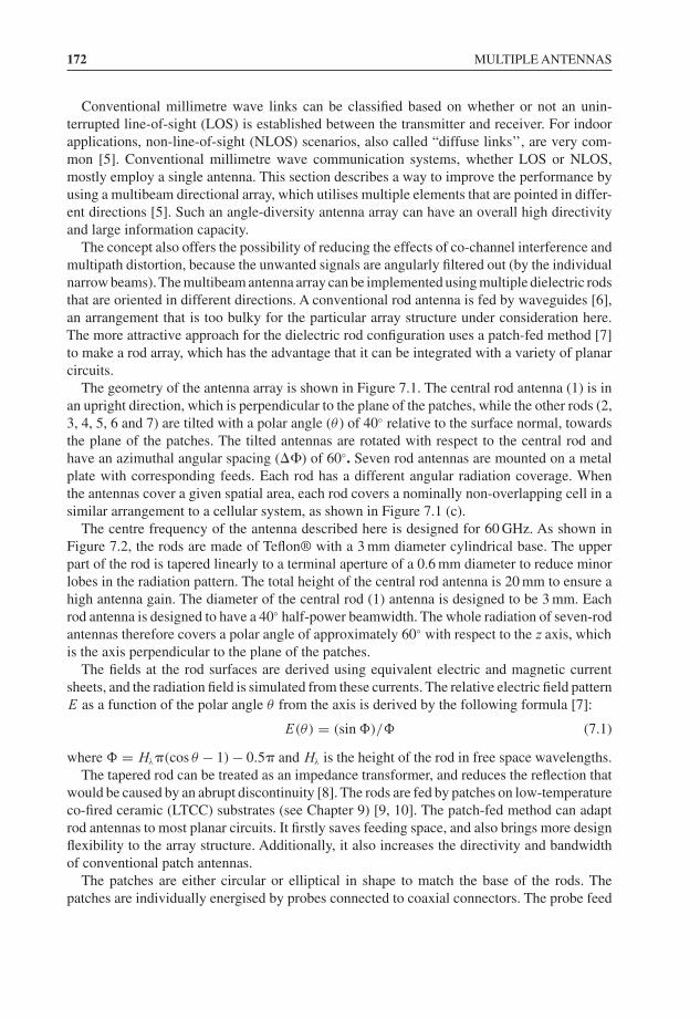
172 MULTIPLE ANTENNAS
Conventional millimetre wave links can be classified based on whether or not an unin-terrupted line-of-sight (LOS) is established between the transmitter and receiver. For indoorapplications, non-line-of-sight (NLOS) scenarios, also called “diffuse links’’, are very com-mon [5]. Conventional millimetre wave communication systems, whether LOS or NLOS,mostly employ a single antenna. This section describes a way to improve the performance byusing a multibeam directional array, which utilises multiple elements that are pointed in differ-ent directions [5]. Such an angle-diversity antenna array can have an overall high directivityand large information capacity.
The concept also offers the possibility of reducing the effects of co-channel interference andmultipath distortion, because the unwanted signals are angularly filtered out (by the individualnarrow beams). The multibeam antenna array can be implemented using multiple dielectric rodsthat are oriented in different directions. A conventional rod antenna is fed by waveguides [6],an arrangement that is too bulky for the particular array structure under consideration here.The more attractive approach for the dielectric rod configuration uses a patch-fed method [7]to make a rod array, which has the advantage that it can be integrated with a variety of planarcircuits.
The geometry of the antenna array is shown in Figure 7.1. The central rod antenna (1) is inan upright direction, which is perpendicular to the plane of the patches, while the other rods (2,3, 4, 5, 6 and 7) are tilted with a polar angle (θ ) of 40◦ relative to the surface normal, towardsthe plane of the patches. The tilted antennas are rotated with respect to the central rod andhave an azimuthal angular spacing (��) of 60◦. Seven rod antennas are mounted on a metalplate with corresponding feeds. Each rod has a different angular radiation coverage. Whenthe antennas cover a given spatial area, each rod covers a nominally non-overlapping cell in asimilar arrangement to a cellular system, as shown in Figure 7.1 (c).
The centre frequency of the antenna described here is designed for 60 GHz. As shown inFigure 7.2, the rods are made of Teflon® with a 3 mm diameter cylindrical base. The upperpart of the rod is tapered linearly to a terminal aperture of a 0.6 mm diameter to reduce minorlobes in the radiation pattern. The total height of the central rod antenna is 20 mm to ensure ahigh antenna gain. The diameter of the central rod (1) antenna is designed to be 3 mm. Eachrod antenna is designed to have a 40◦ half-power beamwidth. The whole radiation of seven-rodantennas therefore covers a polar angle of approximately 60◦ with respect to the z axis, whichis the axis perpendicular to the plane of the patches.
The fields at the rod surfaces are derived using equivalent electric and magnetic currentsheets, and the radiation field is simulated from these currents. The relative electric field patternE as a function of the polar angle θ from the axis is derived by the following formula [7]:
E(θ) = (sin �)/� (7.1)
where � = Hλ�(cos θ − 1) − 0.5� and Hλ is the height of the rod in free space wavelengths.The tapered rod can be treated as an impedance transformer, and reduces the reflection that
would be caused by an abrupt discontinuity [8]. The rods are fed by patches on low-temperatureco-fired ceramic (LTCC) substrates (see Chapter 9) [9, 10]. The patch-fed method can adaptrod antennas to most planar circuits. It firstly saves feeding space, and also brings more designflexibility to the array structure. Additionally, it also increases the directivity and bandwidthof conventional patch antennas.
The patches are either circular or elliptical in shape to match the base of the rods. Thepatches are individually energised by probes connected to coaxial connectors. The probe feed
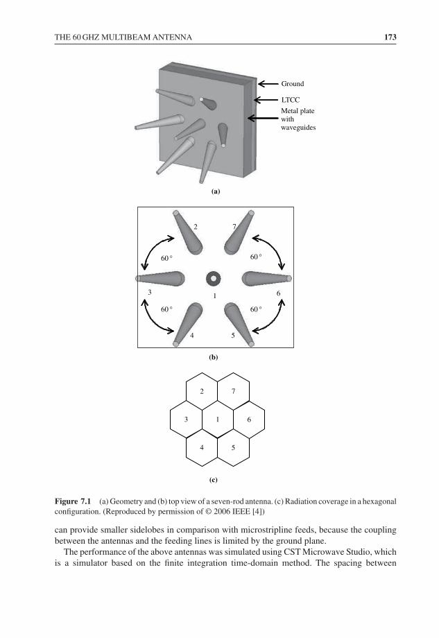
THE 60 GHZ MULTIBEAM ANTENNA 173
(a)
(b)
(c)
Ground
LTCC
Metal platewithwaveguides
1
2
3
4 5
6
7
60 °
60 °60 °
60 °
1
2
3
4 5
6
7
Figure 7.1 (a) Geometry and (b) top view of a seven-rod antenna. (c) Radiation coverage in a hexagonalconfiguration. (Reproduced by permission of © 2006 IEEE [4])
can provide smaller sidelobes in comparison with microstripline feeds, because the couplingbetween the antennas and the feeding lines is limited by the ground plane.
The performance of the above antennas was simulated using CST Microwave Studio, whichis a simulator based on the finite integration time-domain method. The spacing between
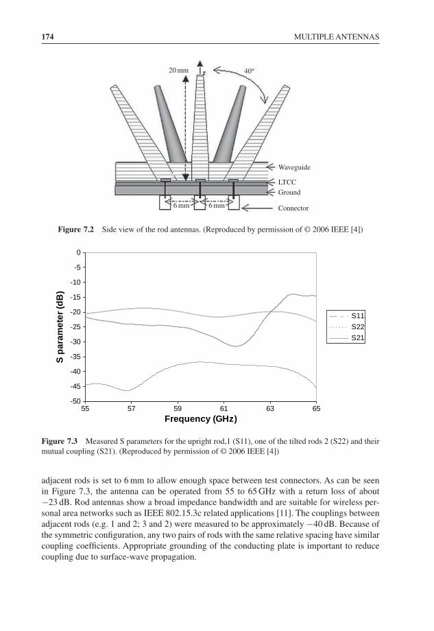
174 MULTIPLE ANTENNAS
6 mm 6 mm
20 mm 40°
Waveguide
LTCCGround
Connector
Figure 7.2 Side view of the rod antennas. (Reproduced by permission of © 2006 IEEE [4])
-50
-45
-40
-35
-30
-25
-20
-15
-10
-5
0
55 57 59 61 63 65
Frequency (GHz)
S p
aram
eter
(dB
)
S11
S22
S21
Figure 7.3 Measured S parameters for the upright rod,1 (S11), one of the tilted rods 2 (S22) and theirmutual coupling (S21). (Reproduced by permission of © 2006 IEEE [4])
adjacent rods is set to 6 mm to allow enough space between test connectors. As can be seenin Figure 7.3, the antenna can be operated from 55 to 65 GHz with a return loss of about−23 dB. Rod antennas show a broad impedance bandwidth and are suitable for wireless per-sonal area networks such as IEEE 802.15.3c related applications [11]. The couplings betweenadjacent rods (e.g. 1 and 2; 3 and 2) were measured to be approximately −40 dB. Because ofthe symmetric configuration, any two pairs of rods with the same relative spacing have similarcoupling coefficients. Appropriate grounding of the conducting plate is important to reducecoupling due to surface-wave propagation.
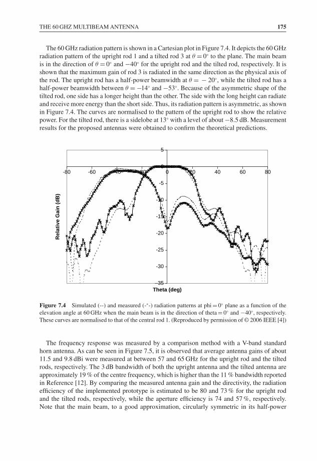
THE 60 GHZ MULTIBEAM ANTENNA 175
The 60 GHz radiation pattern is shown in a Cartesian plot in Figure 7.4. It depicts the 60 GHzradiation pattern of the upright rod 1 and a tilted rod 3 at θ = 0◦ to the plane. The main beamis in the direction of θ = 0◦ and −40◦ for the upright rod and the tilted rod, respectively. It isshown that the maximum gain of rod 3 is radiated in the same direction as the physical axis ofthe rod. The upright rod has a half-power beamwidth at θ = − 20◦, while the tilted rod has ahalf-power beamwidth between θ = −14◦ and −53◦. Because of the asymmetric shape of thetilted rod, one side has a longer height than the other. The side with the long height can radiateand receive more energy than the short side. Thus, its radiation pattern is asymmetric, as shownin Figure 7.4. The curves are normalised to the pattern of the upright rod to show the relativepower. For the tilted rod, there is a sidelobe at 13◦ with a level of about −8.5 dB. Measurementresults for the proposed antennas were obtained to confirm the theoretical predictions.
–35
-30
-25
-20
-15
-10
-5
0
5
-80 -60 -40 -20 0 20 40 60 80
Theta (deg)
Rel
ativ
e G
ain
(d
B)
Figure 7.4 Simulated (--) and measured (-∗-) radiation patterns at phi = 0◦ plane as a function of theelevation angle at 60 GHz when the main beam is in the direction of theta = 0◦ and −40◦, respectively.These curves are normalised to that of the central rod 1. (Reproduced by permission of © 2006 IEEE [4])
The frequency response was measured by a comparison method with a V-band standardhorn antenna. As can be seen in Figure 7.5, it is observed that average antenna gains of about11.5 and 9.8 dBi were measured at between 57 and 65 GHz for the upright rod and the tiltedrods, respectively. The 3 dB bandwidth of both the upright antenna and the tilted antenna areapproximately 19 % of the centre frequency, which is higher than the 11 % bandwidth reportedin Reference [12]. By comparing the measured antenna gain and the directivity, the radiationefficiency of the implemented prototype is estimated to be 80 and 73 % for the upright rodand the tilted rods, respectively, while the aperture efficiency is 74 and 57 %, respectively.Note that the main beam, to a good approximation, circularly symmetric in its half-power
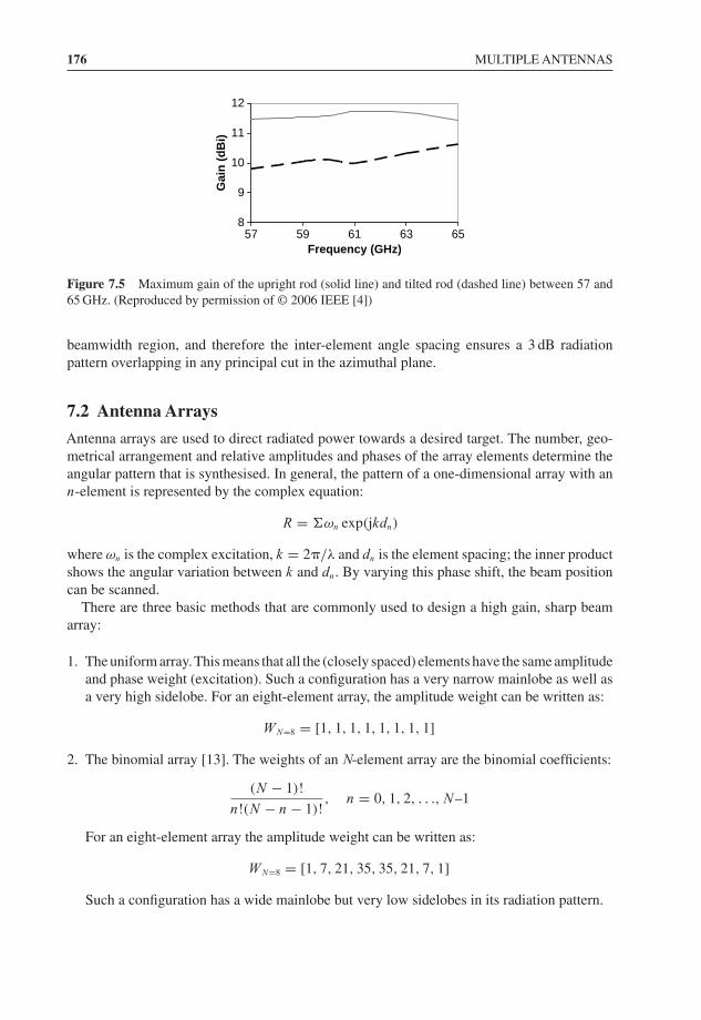
176 MULTIPLE ANTENNAS
8
9
10
11
12
57 59 61 63 65Frequency (GHz)
Gai
n (
dB
i)
Figure 7.5 Maximum gain of the upright rod (solid line) and tilted rod (dashed line) between 57 and65 GHz. (Reproduced by permission of © 2006 IEEE [4])
beamwidth region, and therefore the inter-element angle spacing ensures a 3 dB radiationpattern overlapping in any principal cut in the azimuthal plane.
7.2 Antenna Arrays
Antenna arrays are used to direct radiated power towards a desired target. The number, geo-metrical arrangement and relative amplitudes and phases of the array elements determine theangular pattern that is synthesised. In general, the pattern of a one-dimensional array with ann-element is represented by the complex equation:
R = �ωn exp(jkdn)
where ωn is the complex excitation, k = 2�/λ and dn is the element spacing; the inner productshows the angular variation between k and dn. By varying this phase shift, the beam positioncan be scanned.
There are three basic methods that are commonly used to design a high gain, sharp beamarray:
1. The uniform array.This means that all the (closely spaced) elements have the same amplitudeand phase weight (excitation). Such a configuration has a very narrow mainlobe as well asa very high sidelobe. For an eight-element array, the amplitude weight can be written as:
WN=8 = [1, 1, 1, 1, 1, 1, 1, 1]2. The binomial array [13]. The weights of an N-element array are the binomial coefficients:
(N − 1)!
n!(N − n − 1)!, n = 0, 1, 2, . . ., N–1
For an eight-element array the amplitude weight can be written as:
WN=8 = [1, 7, 21, 35, 35, 21, 7, 1]Such a configuration has a wide mainlobe but very low sidelobes in its radiation pattern.
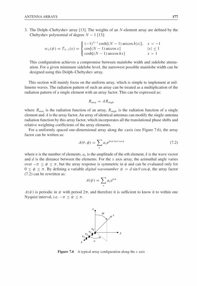
ANTENNA ARRAYS 177
3. The Dolph–Chebyshev array [13]. The weights of an N -element array are defined by theChebyshev polynomial of degree N − 1 [13]:
wN(ψ) = TN−1(x) =⎧⎨⎩
(−1)N−1 cosh[(N − 1) arccos h|x|], x < −1cos[(N − 1) arccos x] |x| ≤ 1cosh[(N − 1) arccos hx] x > 1
This configuration achieves a compromise between mainlobe width and sidelobe attenu-ation. For a given minimum sidelobe level, the narrowest possible mainlobe width can bedesigned using this Dolph–Chebyshev array.
This section will mainly focus on the uniform array, which is simple to implement at mil-limetre waves. The radiation pattern of such an array can be treated as a multiplication of theradiation pattern of a single element with an array factor. This can be expressed as:
Rarray = ARsingle
where Rarray is the radiation function of an array, Rsingle is the radiation function of a singleelement and A is the array factor. An array of identical antennas can modify the single-antennaradiation function by this array factor, which incorporates all the translational phase shifts andrelative weighting coefficients of the array elements.
For a uniformly spaced one-dimensional array along the xaxis (see Figure 7.6), the arrayfactor can be written as:
A(θ, φ) =∑
n
anejknd sin θ cos φ (7.2)
where n is the number of elements, an is the amplitude of the nth element, k is the wave vectorand d is the distance between the elements. For the x axis array, the azimuthal angle variesover −π ≤ φ ≤ π , but the array response is symmetric in φ and can be evaluated only for0 ≤ φ ≤ π . By defining a variable digital wavenumber ψ = d sin θ cos φ, the array factor(7.2) can be rewritten as:
A(ψ) =∑
n
anejnψ
A(ψ) is periodic in ψ with period 2�, and therefore it is sufficient to know it to within oneNyquist interval, i.e. −π ≤ ψ ≤ π .
x
y
φ
θz
r
x1x2x3
x0
Figure 7.6 A typical array configuration along the x axis
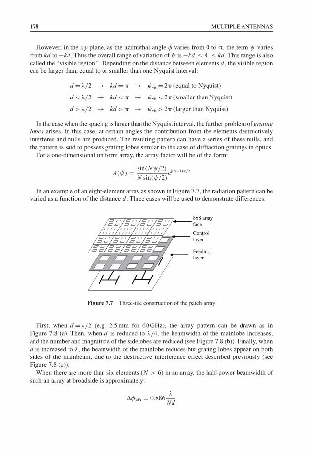
178 MULTIPLE ANTENNAS
However, in the xy plane, as the azimuthal angle φ varies from 0 to �, the term ψ variesfrom kd to −kd. Thus the overall range of variation of ψ is −kd ≤ ≤ kd. This range is alsocalled the “visible region’’. Depending on the distance between elements d, the visible regioncan be larger than, equal to or smaller than one Nyquist interval:
d = λ/2 → kd = � → ψvis = 2� (equal to Nyquist)
d < λ/2 → kd < � → ψvis < 2� (smaller than Nyquist)
d > λ/2 → kd > � → ψvis > 2� (larger than Nyquist)
In the case when the spacing is larger than the Nyquist interval, the further problem of gratinglobes arises. In this case, at certain angles the contribution from the elements destructivelyinterferes and nulls are produced. The resulting pattern can have a series of these nulls, andthe pattern is said to possess grating lobes similar to the case of diffraction gratings in optics.
For a one-dimensional uniform array, the array factor will be of the form:
A(ψ) = sin(Nψ/2)
N sin(ψ/2)ej(N−1)ψ/2
In an example of an eight-element array as shown in Figure 7.7, the radiation pattern can bevaried as a function of the distance d . Three cases will be used to demonstrate differences.
8x8 array face
Controllayer
Feedinglayer
Figure 7.7 Three-tile construction of the patch array
First, when d = λ/2 (e.g. 2.5 mm for 60 GHz), the array pattern can be drawn as inFigure 7.8 (a). Then, when d is reduced to λ/4, the beamwidth of the mainlobe increases,and the number and magnitude of the sidelobes are reduced (see Figure 7.8 (b)). Finally, whend is increased to λ, the beamwidth of the mainlobe reduces but grating lobes appear on bothsides of the mainbeam, due to the destructive interference effect described previously (seeFigure 7.8 (c)).
When there are more than six elements (N > 6) in an array, the half-power beamwidth ofsuch an array at broadside is approximately:
�φ3dB = 0.886λ
Nd
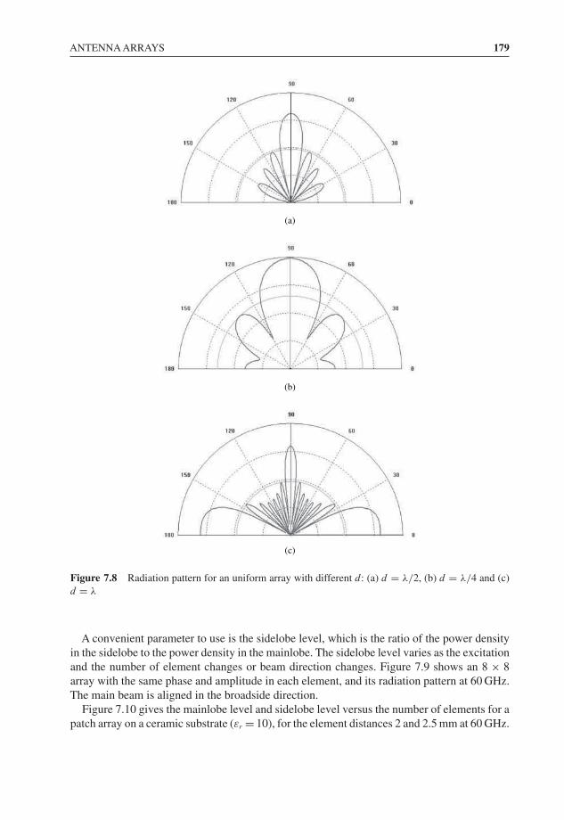
ANTENNA ARRAYS 179
(b)
(c)
(a)
Figure 7.8 Radiation pattern for an uniform array with different d: (a) d = λ/2, (b) d = λ/4 and (c)d = λ
A convenient parameter to use is the sidelobe level, which is the ratio of the power densityin the sidelobe to the power density in the mainlobe. The sidelobe level varies as the excitationand the number of element changes or beam direction changes. Figure 7.9 shows an 8 × 8array with the same phase and amplitude in each element, and its radiation pattern at 60 GHz.The main beam is aligned in the broadside direction.
Figure 7.10 gives the mainlobe level and sidelobe level versus the number of elements for apatch array on a ceramic substrate (εr = 10), for the element distances 2 and 2.5 mm at 60 GHz.
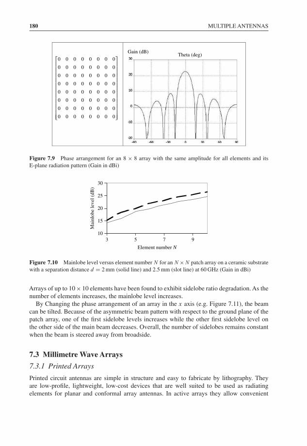
180 MULTIPLE ANTENNAS
⎥⎥⎥⎥⎥⎥⎥⎥⎥⎥⎥
⎦
⎤
⎢⎢⎢⎢⎢⎢⎢⎢⎢⎢⎢
⎣
⎡
00000000
00000000
00000000
00000000
00000000
00000000
00000000
00000000Theta (deg)
Gain (dB)
Figure 7.9 Phase arrangement for an 8 × 8 array with the same amplitude for all elements and itsE-plane radiation pattern (Gain in dBi)
10
15
20
25
30
3 5 7 9
Element number N
Mai
nlob
e le
vel (
dB)
Figure 7.10 Mainlobe level versus element number N for an N ×N patch array on a ceramic substratewith a separation distance d = 2 mm (solid line) and 2.5 mm (slot line) at 60 GHz (Gain in dBi)
Arrays of up to 10 × 10 elements have been found to exhibit sidelobe ratio degradation. As thenumber of elements increases, the mainlobe level increases.
By Changing the phase arrangement of an array in the x axis (e.g. Figure 7.11), the beamcan be tilted. Because of the asymmetric beam pattern with respect to the ground plane of thepatch array, one of the first sidelobe levels increases while the other first sidelobe level onthe other side of the main beam decreases. Overall, the number of sidelobes remains constantwhen the beam is steered away from broadside.
7.3 Millimetre Wave Arrays
7.3.1 Printed Arrays
Printed circuit antennas are simple in structure and easy to fabricate by lithography. Theyare low-profile, lightweight, low-cost devices that are well suited to be used as radiatingelements for planar and conformal array antennas. In active arrays they allow convenient
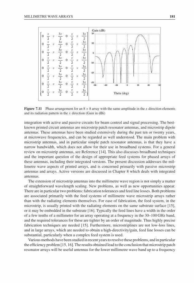
MILLIMETRE WAVE ARRAYS 181
⎥⎥⎥⎥⎥⎥⎥⎥⎥⎥⎥⎥⎥⎥⎥⎥⎥⎥
⎦
⎤
⎢⎢⎢⎢⎢⎢⎢⎢⎢⎢⎢⎢⎢⎢⎢⎢⎢⎢
⎣
⎡
220
220
220
220
220
220
220
220
220
220
220
220
220
220
220
2
3π
3π
3π
3π
3π
3π
3π
3π
3π
3π
3π
3π
3π
3π
3π
3π2
0
ππ
ππ
ππ
ππ
ππ
ππ
ππ
ππ
ππ
ππ
ππ
ππ
ππ
ππ
ππ
ππ
Theta (deg)
Gain (dB)
Figure 7.11 Phase arrangement for an 8 × 8 array with the same amplitude in the x direction elementsand its radiation pattern in the x direction (Gain in dBi)
integration with active and passive circuits for beam control and signal processing. The best-known printed circuit antennas are microstrip patch resonator antennas, and microstrip dipoleantennas. These antennas have been studied extensively during the past ten or twenty years,at microwave frequencies, and can be regarded as well understood. The main problem withmicrostrip antennas, and in particular simple patch resonator antennas, is that they have anarrow bandwidth, which does not allow for their use in broadband systems. For a generalreview on microstrip antennas, see Reference [14]. This also discusses broadband techniquesand the important question of the design of appropriate feed systems for phased arrays ofthese antennas, including their integrated versions. The present discussion addresses the mil-limetre wave aspects of printed arrays, and is concerned primarily with passive microstripantennas and arrays. Active versions are discussed in Chapter 8 which deals with integratedantennas.
The extension of microstrip antennas into the millimetre wave region is not simply a matterof straightforward wavelength scaling. New problems, as well as new opportunities appear.There are in particular two problems: fabrication tolerances and feed line losses. Both problemsare associated primarily with the feed systems of millimetre wave microstrip arrays ratherthan with the radiating elements themselves. For ease of fabrication, the feed system, in themicrostrip, is usually printed with the radiating elements on the same substrate surface [15],or it may be embedded in the substrate [16]. Typically the feed lines have a width in the orderof a few tenths of a millimetre for an array operating at a frequency in the 30–100 GHz band,and the required tolerances for these are tighter by an order of magnitude. Thus highly precisefabrication techniques are needed [15]. Furthermore, microstriplines are not low-loss lines,and in large arrays, which are needed to obtain a high-directivity/gain, feed line losses can besubstantial, particularly when a complex feed system is used.
Various methods have been studied in recent years to resolve these problems, and in particularthe efficiency problem [15, 16]. The results obtained lead to the conclusion that microstrip patchresonator arrays will be useful antennas for the lower millimetre wave band up to a frequency
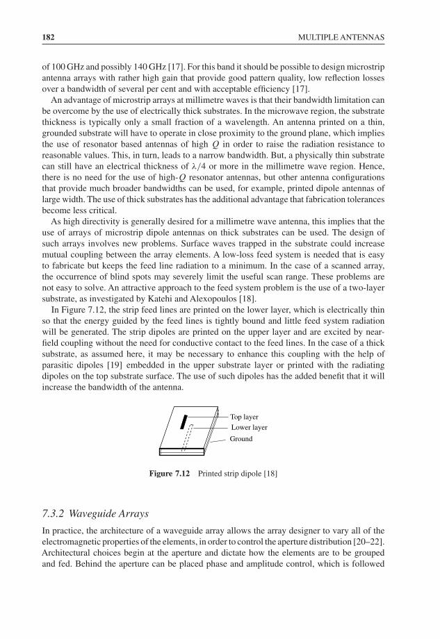
182 MULTIPLE ANTENNAS
of 100 GHz and possibly 140 GHz [17]. For this band it should be possible to design microstripantenna arrays with rather high gain that provide good pattern quality, low reflection lossesover a bandwidth of several per cent and with acceptable efficiency [17].
An advantage of microstrip arrays at millimetre waves is that their bandwidth limitation canbe overcome by the use of electrically thick substrates. In the microwave region, the substratethickness is typically only a small fraction of a wavelength. An antenna printed on a thin,grounded substrate will have to operate in close proximity to the ground plane, which impliesthe use of resonator based antennas of high Q in order to raise the radiation resistance toreasonable values. This, in turn, leads to a narrow bandwidth. But, a physically thin substratecan still have an electrical thickness of λ/4 or more in the millimetre wave region. Hence,there is no need for the use of high-Q resonator antennas, but other antenna configurationsthat provide much broader bandwidths can be used, for example, printed dipole antennas oflarge width. The use of thick substrates has the additional advantage that fabrication tolerancesbecome less critical.
As high directivity is generally desired for a millimetre wave antenna, this implies that theuse of arrays of microstrip dipole antennas on thick substrates can be used. The design ofsuch arrays involves new problems. Surface waves trapped in the substrate could increasemutual coupling between the array elements. A low-loss feed system is needed that is easyto fabricate but keeps the feed line radiation to a minimum. In the case of a scanned array,the occurrence of blind spots may severely limit the useful scan range. These problems arenot easy to solve. An attractive approach to the feed system problem is the use of a two-layersubstrate, as investigated by Katehi and Alexopoulos [18].
In Figure 7.12, the strip feed lines are printed on the lower layer, which is electrically thinso that the energy guided by the feed lines is tightly bound and little feed system radiationwill be generated. The strip dipoles are printed on the upper layer and are excited by near-field coupling without the need for conductive contact to the feed lines. In the case of a thicksubstrate, as assumed here, it may be necessary to enhance this coupling with the help ofparasitic dipoles [19] embedded in the upper substrate layer or printed with the radiatingdipoles on the top substrate surface. The use of such dipoles has the added benefit that it willincrease the bandwidth of the antenna.
Top layer
Lower layer
Ground
Figure 7.12 Printed strip dipole [18]
7.3.2 Waveguide Arrays
In practice, the architecture of a waveguide array allows the array designer to vary all of theelectromagnetic properties of the elements, in order to control the aperture distribution [20–22].Architectural choices begin at the aperture and dictate how the elements are to be groupedand fed. Behind the aperture can be placed phase and amplitude control, which is followed
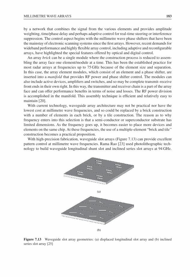
MILLIMETRE WAVE ARRAYS 183
by a network that combines the signal from the various elements and provides amplitudeweighting, time/phase delay and perhaps adaptive control for real-time steering or interferencesuppression. The control aspect begins with the millimetre wave phase shifters that have beenthe mainstay of electronic scanning systems since the first arrays. However, recent demands forwideband performance and highly flexible array control, including adaptive and reconfigurablearrays, have highlighted the special features offered by optical and digital control.
An array brick can be a single module where the construction process is reduced to assem-bling the array face one element/module at a time. This has been the established practice formost radar arrays at frequencies up to 75 GHz because of the element size and separation.In this case, the array element modules, which consist of an element and a phase shifter, areinserted into a manifold that provides RF power and phase shifter control. The modules canalso include active devices, amplifiers and switches, and so may be complete transmit–receivefront ends in their own right. In this way, the transmitter and receiver chain is a part of the arrayface and can offer performance benefits in terms of noise and losses. The RF power divisionis accomplished in the manifold. This assembly technique is efficient and relatively easy tomaintain [20].
With current technology, waveguide array architecture may not be practical nor have thelowest cost at millimetre wave frequencies, and so could be replaced by a brick constructionwith a number of elements in each brick, or by a tile construction. The reason as to whyfrequency enters into this selection is that a semi-conductor or superconductor substrate haslimited dimensions. As the frequency goes up, it becomes easier to place more devices andelements on the same chip. At these frequencies, the use of a multiple-element “brick and tile’’construction becomes a practical proposition.
With high-precision fabrication, waveguide slot arrays (Figure 7.13) can provide excellentpattern control at millimetre wave frequencies. Rama Rao [23] used photolithographic tech-nology to build waveguide longitudinal shunt slot and inclined series slot arrays at 94 GHz.
(a)
(b)
Figure 7.13 Waveguide slot array geometries: (a) displaced longitudinal slot array and (b) inclinedseries slot array [25]
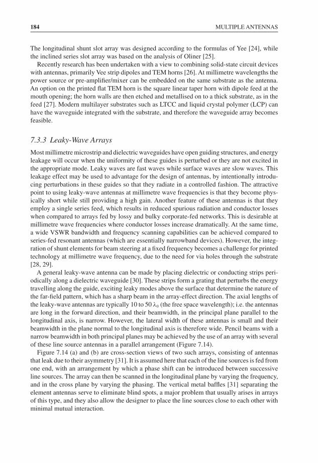
184 MULTIPLE ANTENNAS
The longitudinal shunt slot array was designed according to the formulas of Yee [24], whilethe inclined series slot array was based on the analysis of Oliner [25].
Recently research has been undertaken with a view to combining solid-state circuit deviceswith antennas, primarily Vee strip dipoles and TEM horns [26]. At millimetre wavelengths thepower source or pre-amplifier/mixer can be embedded on the same substrate as the antenna.An option on the printed flat TEM horn is the square linear taper horn with dipole feed at themouth opening; the horn walls are then etched and metallised on to a thick substrate, as in thefeed [27]. Modern multilayer substrates such as LTCC and liquid crystal polymer (LCP) canhave the waveguide integrated with the substrate, and therefore the waveguide array becomesfeasible.
7.3.3 Leaky-Wave Arrays
Most millimetre microstrip and dielectric waveguides have open guiding structures, and energyleakage will occur when the uniformity of these guides is perturbed or they are not excited inthe appropriate mode. Leaky waves are fast waves while surface waves are slow waves. Thisleakage effect may be used to advantage for the design of antennas, by intentionally introdu-cing perturbations in these guides so that they radiate in a controlled fashion. The attractivepoint to using leaky-wave antennas at millimetre wave frequencies is that they become phys-ically short while still providing a high gain. Another feature of these antennas is that theyemploy a single series feed, which results in reduced spurious radiation and conductor losseswhen compared to arrays fed by lossy and bulky corporate-fed networks. This is desirable atmillimetre wave frequencies where conductor losses increase dramatically. At the same time,a wide VSWR bandwidth and frequency scanning capabilities can be achieved compared toseries-fed resonant antennas (which are essentially narrowband devices). However, the integ-ration of shunt elements for beam steering at a fixed frequency becomes a challenge for printedtechnology at millimetre wave frequency, due to the need for via holes through the substrate[28, 29].
A general leaky-wave antenna can be made by placing dielectric or conducting strips peri-odically along a dielectric waveguide [30]. These strips form a grating that perturbs the energytravelling along the guide, exciting leaky modes above the surface that determine the nature ofthe far-field pattern, which has a sharp beam in the array-effect direction. The axial lengths ofthe leaky-wave antennas are typically 10 to 50 λ0 (the free space wavelength); i.e. the antennasare long in the forward direction, and their beamwidth, in the principal plane parallel to thelongitudinal axis, is narrow. However, the lateral width of these antennas is small and theirbeamwidth in the plane normal to the longitudinal axis is therefore wide. Pencil beams with anarrow beamwidth in both principal planes may be achieved by the use of an array with severalof these line source antennas in a parallel arrangement (Figure 7.14).
Figure 7.14 (a) and (b) are cross-section views of two such arrays, consisting of antennasthat leak due to their asymmetry [31]. It is assumed here that each of the line sources is fed fromone end, with an arrangement by which a phase shift can be introduced between successiveline sources. The array can then be scanned in the longitudinal plane by varying the frequency,and in the cross plane by varying the phasing. The vertical metal baffles [31] separating theelement antennas serve to eliminate blind spots, a major problem that usually arises in arraysof this type, and they also allow the designer to place the line sources close to each other withminimal mutual interaction.
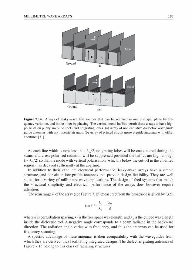
MILLIMETRE WAVE ARRAYS 185
(b)
E
E
εr
Metal
E
E
Metal
Ground
Ground(a)
εr
Figure 7.14 Arrays of leaky-wave line sources that can be scanned in one principal plane by fre-quency variation, and in the other by phasing. The vertical metal baffles permit these arrays to have highpolarisation purity, no blind spots and no grating lobes. (a) Array of non-radiative dielectric waveguideguide antennas with asymmetric air gaps. (b) Array of printed circuit groove-guide antennas with offsetapertures [31]
As each line width is now less than λ0/2, no grating lobes will be encountered during thescans, and cross polarised radiation will be suppressed provided the baffles are high enough(> λ0/2) so that the mode with vertical polarisation (which is below the cut-off in the air-filledregion) has decayed sufficiently at the aperture.
In addition to their excellent electrical performance, leaky-wave arrays have a simplestructure, and constitute low-profile antennas that provide design flexibility. They are wellsuited for a variety of millimetre wave applications. The design of feed systems that matchthe structural simplicity and electrical performance of the arrays does however requireattention.
The scan range θ of the array (see Figure 7.15) measured from the broadside is given by [32]:
sin θ ≈ λ0
λg
− λ0
d
where d is perturbation spacing, λ0 is the free space wavelength, and λg is the guided wavelengthinside the dielectric rod. A negative angle corresponds to a beam radiated in the backwarddirection. The radiation angle varies with frequency, and thus the antennas can be used forfrequency scanning.
A specific advantage of these antennas is their compatibility with the waveguides fromwhich they are derived, thus facilitating integrated designs. The dielectric grating antennas ofFigure 7.15 belong to this class of radiating structures.
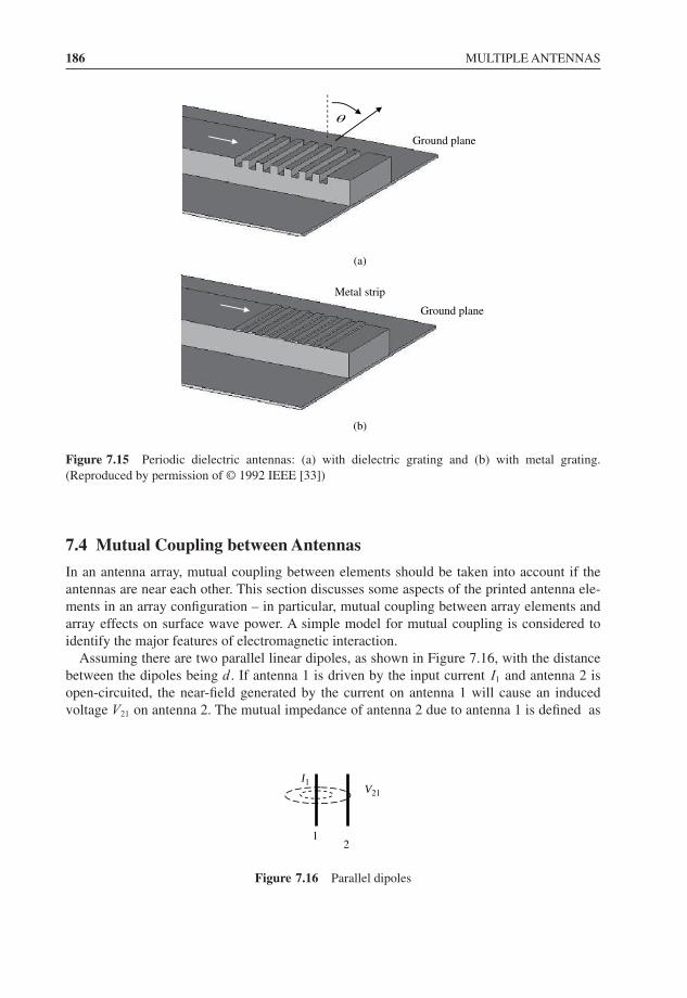
186 MULTIPLE ANTENNAS
(a)
θ
(b)
Metal strip
Ground plane
Ground plane
Figure 7.15 Periodic dielectric antennas: (a) with dielectric grating and (b) with metal grating.(Reproduced by permission of © 1992 IEEE [33])
7.4 Mutual Coupling between Antennas
In an antenna array, mutual coupling between elements should be taken into account if theantennas are near each other. This section discusses some aspects of the printed antenna ele-ments in an array configuration – in particular, mutual coupling between array elements andarray effects on surface wave power. A simple model for mutual coupling is considered toidentify the major features of electromagnetic interaction.
Assuming there are two parallel linear dipoles, as shown in Figure 7.16, with the distancebetween the dipoles being d . If antenna 1 is driven by the input current I1 and antenna 2 isopen-circuited, the near-field generated by the current on antenna 1 will cause an inducedvoltage V21 on antenna 2. The mutual impedance of antenna 2 due to antenna 1 is defined as
I1V21
12
Figure 7.16 Parallel dipoles
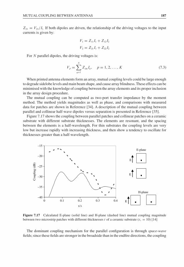
MUTUAL COUPLING BETWEEN ANTENNAS 187
Z21 = V21/I1. If both dipoles are driven, the relationship of the driving voltages to the inputcurrents is given by:
V1 = Z11I1 + Z12I2
V2 = Z21I1 + Z22I2
For N parallel dipoles, the driving voltages is:
Vp =N∑
q=1
ZpqIq, p = 1, 2, . . . , K (7.3)
When printed antenna elements form an array, mutual coupling levels could be large enoughto degrade sidelobe levels and main beam shape, and cause array blindness. These effects can beminimised with the knowledge of coupling between the array elements and its proper inclusionin the array design procedure.
The mutual coupling can be computed as two-port transfer impedance by the momentmethod. The method yields magnitudes as well as phase, and comparisons with measureddata for patches are shown in Reference [34]. A description of the mutual coupling betweenparallel and collinear half-wave dipoles versus separation is presented in Reference [35].
Figure 7.17 shows the coupling between parallel patches and collinear patches on a ceramicsubstrate with different substrate thicknesses. The elements are resonant, and the spacingbetween the elements is a half-wavelength. For thin substrates the coupling levels are verylow but increase rapidly with increasing thickness, and then show a tendency to oscillate forthicknesses greater than a half-wavelength.
–40
–35
–30
–25
–20
–15
0 0.1 0.2 0.3 0.4
t /λ
Cou
plin
g (d
B)
E-plane
H-plane
E
E
E
Figure 7.17 Calculated E-plane (solid line) and H-plane (dashed line) mutual coupling magnitudebetween two microstrip patches with different thicknesses t of a ceramic substrate (εr = 10) [14]
The dominant coupling mechanism for the parallel configuration is through space-wavefields; since these fields are stronger in the broadside than in the endfire directions, the coupling
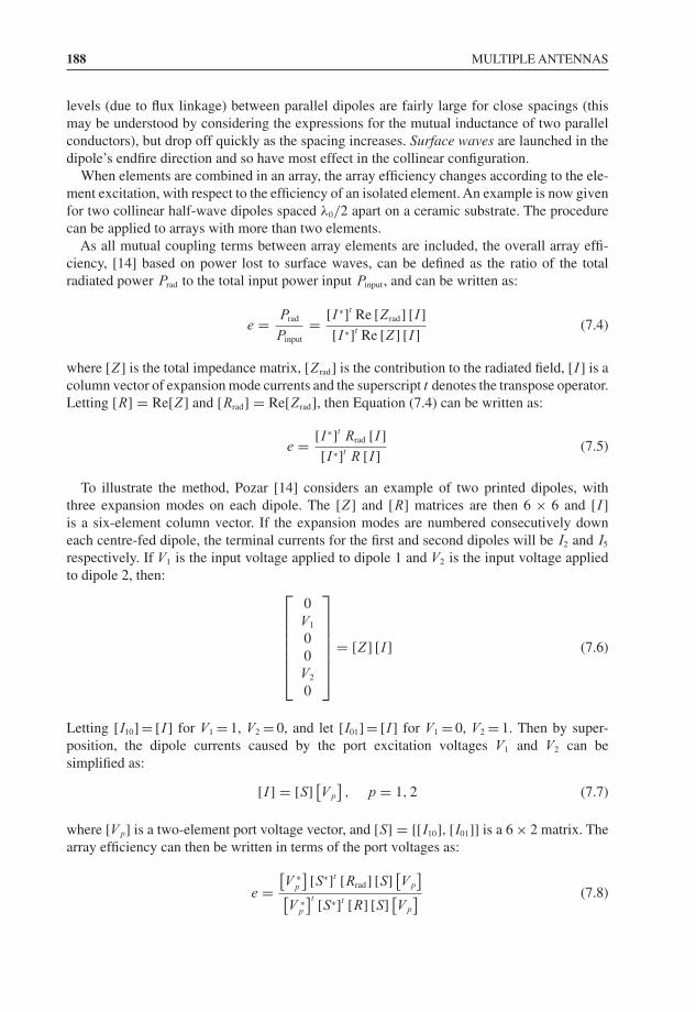
188 MULTIPLE ANTENNAS
levels (due to flux linkage) between parallel dipoles are fairly large for close spacings (thismay be understood by considering the expressions for the mutual inductance of two parallelconductors), but drop off quickly as the spacing increases. Surface waves are launched in thedipole’s endfire direction and so have most effect in the collinear configuration.
When elements are combined in an array, the array efficiency changes according to the ele-ment excitation, with respect to the efficiency of an isolated element. An example is now givenfor two collinear half-wave dipoles spaced λ0/2 apart on a ceramic substrate. The procedurecan be applied to arrays with more than two elements.
As all mutual coupling terms between array elements are included, the overall array effi-ciency, [14] based on power lost to surface waves, can be defined as the ratio of the totalradiated power Prad to the total input power input Pinput, and can be written as:
e = Prad
Pinput
= [I ∗]t Re [Zrad] [I ]
[I ∗]t Re [Z] [I ](7.4)
where [Z] is the total impedance matrix, [Zrad] is the contribution to the radiated field, [I ] is acolumn vector of expansion mode currents and the superscript t denotes the transpose operator.Letting [R] = Re[Z] and [Rrad] = Re[Zrad], then Equation (7.4) can be written as:
e = [I ∗]tRrad [I ]
[I ∗]tR [I ]
(7.5)
To illustrate the method, Pozar [14] considers an example of two printed dipoles, withthree expansion modes on each dipole. The [Z] and [R] matrices are then 6 × 6 and [I ]is a six-element column vector. If the expansion modes are numbered consecutively downeach centre-fed dipole, the terminal currents for the first and second dipoles will be I2 and I5
respectively. If V1 is the input voltage applied to dipole 1 and V2 is the input voltage appliedto dipole 2, then: ⎡
⎢⎢⎢⎢⎢⎢⎣
0V1
00V2
0
⎤⎥⎥⎥⎥⎥⎥⎦
= [Z] [I ] (7.6)
Letting [I10] = [I ] for V1 = 1, V2 = 0, and let [I01] = [I ] for V1 = 0, V2 = 1. Then by super-position, the dipole currents caused by the port excitation voltages V1 and V2 can besimplified as:
[I ] = [S][Vp
], p = 1, 2 (7.7)
where [Vp] is a two-element port voltage vector, and [S] = [[I10], [I01]] is a 6 × 2 matrix. Thearray efficiency can then be written in terms of the port voltages as:
e =[V ∗
p
][S∗]t [Rrad] [S]
[Vp
][V ∗
p
]t[S∗]t [R] [S]
[Vp
] (7.8)
MUTUAL COUPLING BETWEEN ANTENNAS 189
It is noted that Equation (7.8) describes the performance index e, the efficiency, as a ratio oftwo quadratic forms. Thus, Equation (7.8) can be optimised by solving the eigenvalue equation:
[M][Vp
] = e [N ][Vp
](7.9)
where [M] = [S∗]t [Rrad] [S], and [N ] = [S∗]t [R] [S] are Hermitian 2 × 2 matrices. A similarprocedure has been used for free space array optimisation [36]. If both dipoles are identicalthen, by symmetry, it can be shown that [M] and [N ] have the form:
[M] =[
m1 m2
m2 m1
]and [N ] =
[n1 n2
n2 n1
](7.10)
with m1, m2, n1 and n2 real. The eigenvectors, representing the feed voltages for optimum e,are either even or odd:
[Vp
]even
=[
11
]
[Vp
]odd
=[
1−1
](7.11)
The corresponding eigenvalues are then the efficiencies resulting from the above excitations:
eeven = m1 + m2
n1 + n2
eodd = m1 − m2
n1 − n2
(7.12)
In general, the even mode produces the maximum array efficiency whereas the odd modeproduces the minimum array efficiency. The optimised efficiency e for two collinear half-wavedipoles λ0/2 apart with different substrate thicknesses is shown in Figure 7.18, for even andodd mode excitations. As can be seen, the efficiency of the even mode can be improved byas much as 40 % compared to odd mode excitation. Pozar cites a similar calculation for twoparallel dipoles that shows a 10 % improvement for even mode excitation.
For the data shown in Figure 7.18, the maximum improvement occurs for uniform phaseexcitation of the array elements – which is a practical result for broadside arrays. Odd mode
0
0,2
0,4
0,6
0,8
1
0 0,1 0,2thickness t (mm)
effic
ienc
y
EvenOdd
E-planecoupling
Figure 7.18 Optimised efficiency e for two collinear half-wave dipoles with λ0/2 apart versus theceramic substrate thickness t . (Reproduced by permission of © 1983 IEEE [14])
190 MULTIPLE ANTENNAS
excitation generally produces a reduced efficiency, which means that more power is beingcoupled to surface waves – a result that may be of interest for surface wave antennas. InFigure 7.18, the eeven and eodd curves cross at the substrate thickness at about t = 0.22 mm.
The efficiency variation for planar antenna elements in an array can be partially explained interms of the phasing of the surface wave fields. Surface waves, launched endfire-wise from eachdipole, are significantly out-of-phase (because of the λ0/2 dipole spacing) and tend to canceleach other out. It is postulated that element spacing exists such that the maximum cancellationoccurs, and the efficiency e approaches 100 % (at least for substrate thicknesses where onlyone surface wave mode presents). Nevertheless, this situation is unlikely to happen when thereis more than one surface wave mode, as the different phase constants would preclude totalcancellation.
In addition to the signal coupling between antennas, noise could also couple betweenelements. Recent findings show that the signal-to-noise ratio is affected by mutual coupling,this points to a new issue about the thermal noise behaviour in a multiantenna system. Thissection only concentrates on the thermal noise effect. Other noise effects of concern to anantenna array in a communication system can be found in References [37] and [38].
Thermal noise is produced by the random, excited thermally, motion of electrons in a mater-ial. The performance of a communication system can be defined in terms of a suitable noisetemperature value, TN , chosen so that:
S
N= T
TN
In effect, TN is the temperature of a thermal source, which would provide a signal powerequal to the noise power level. For example, for single-sideband superheterodyne receivers,the noise temperature will be:
TN ≥ 0.048 × f
where TN is in kelvins and f is in GHz. For 60 GHz, the minimum possible noise temperatureis 2.88 K.
Thermal noise plays a key role in MIMO communication systems, which use antenna arraysto increase the communication capacity [34]. High capacity could be achieved in these systemsby ensuring independence of the channel matrix coefficients, a condition normally achievedwith wide antenna element spacing. However, persistent miniaturisation of subscriber unitsmakes such large separations impossible, and the resulting antenna mutual coupling [39] sig-nificantly impacts on the communication system performance. In Reference [40], the noisethat originated from the amplifier at the receiver end of the MIMO system was included in theconsideration, but the thermal noise on the coupled antennas was not considered. The possib-ility that the thermal noise from a radiating body could be induced in the antenna is discussedin Reference [41]. The topic of partially correlated noise sources that might be introduced intoreceivers of two closely spaced antennas is discussed in Reference [42].
The impact of antenna mutual coupling on the MIMO system has been evaluated by examin-ing how the coupled antennas change the signal correlation [40]. The modifications in channelmatrix coefficients are then used to assess mutual coupling effects on the system capacity [43].Also the radiated power at the transmitter and the power collection capability due to the effectof this mutual coupling in the multiantenna systems, are presented in Reference [44]. Theeffect of mutual coupling on the MIMO channel capacity in the context of the signal-to-noiseratio (SNR) is presented in Reference [45].
MUTUAL COUPLING BETWEEN ANTENNAS 191
Thermal noise that originates from the antenna material itself is self-noise or self-radiation.As well as this self-radiated noise, induced thermal noise appears in the antenna from radiatedbodies in the antenna’s vicinity [46].
Thermal noise correlation due to mutual coupling effects in closely spaced antennas wasmissing in the assessment of early MIMO system communication performance with smallantenna element separation, which was especially critical for customer units. However, thesignal-to-noise ratio (SNR) will now be discussed for the multiantenna system case, with a largenumber of antennas placed in an infinitesimally volume of space, which models the antennaspacing as almost zero (or small compared to the free space wavelength). Without consideringthe mutual coupling effect a calculation would give an infinite value for SNR. The resultobtained by using classical methods demonstrates the importance of the proper consideration ofcoupled antennas in multiantenna systems. The expression for the total signal-to-noise ratio is:
SNR = limnR→∞d→0
n2RP
nRN(7.13)
where d is the antenna spacing, and P and N are the signal and noise power, respectively.The multiantenna system can be represented as a general linear network using a general-
ised form of Thévenin’s theorem. The generalisation of the theorem holds true not only forcoherent sources but also for thermal noise sources [47]. It is valid even for a general lin-ear network that may contain a number of inaccessible (hidden) nodes together with internalvoltage and current sources, whose location may be unknown. However, as long as there areonly N independent accessible nodes, such a system is indistinguishable from a noise sourcefree network, with the same impedance or admittance matrix, together with a set of N nodalcurrent generators of infinite internal impedance. The current from the generator of the ithnode, in such an equivalent network, is equal to the current flowing into the rth node of theoriginal network when all nodes of the latter are short-circuited to earth. The internal sourcesmay be alternatively represented by a set of N nodal voltage generators of infinite internaladmittance, such that the voltage across the generators in the rth node is equal to the voltageacross the rth node of the original network; when all the nodes of the latter are open-circuit.The nodal noise sources are not in general independent.
The multiantenna system with N = nR antenna elements, can be represented as a linear nR
terminal-pair network containing internal signals or noise generators; it is specified completelywith respect to its terminal pairs by its admittance matrix Y and a set of nR nodal currentgenerators i1, i2, . . ., inR. In matrix form, Y denotes a squared matrix of order nR:
Y =
⎛⎜⎜⎝
y11 y12 · · · y1nR
y21 y22 · · · y2nR· · · · · · · · · · · ·ynR1 ynR2 · · · ynRnR
⎞⎟⎟⎠ (7.14)
The complex amplitudes of thermal current generators are represented conveniently by acolumn vector i:
i =
⎛⎜⎜⎝
i1
i2
.
inR
⎞⎟⎟⎠ (7.15)
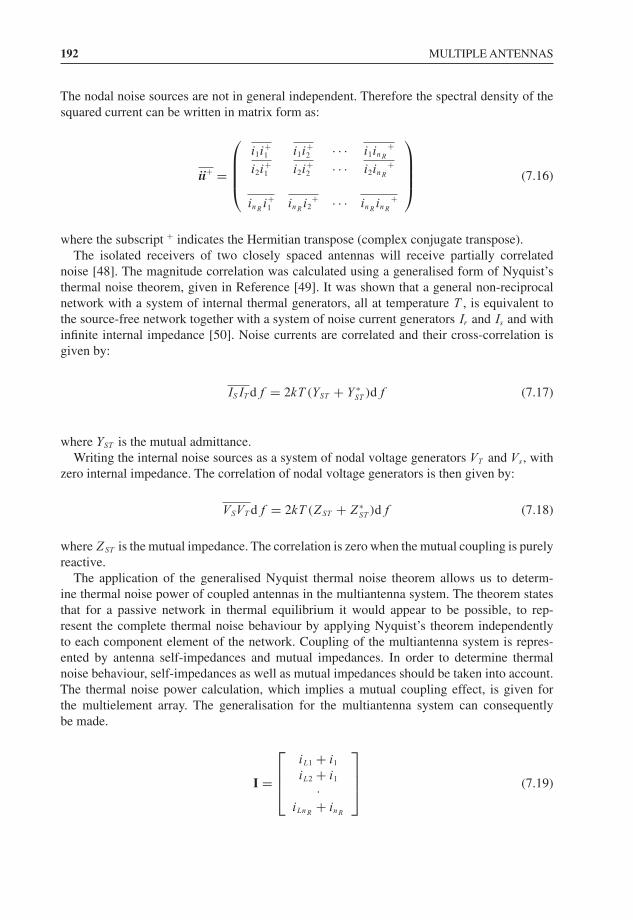
192 MULTIPLE ANTENNAS
The nodal noise sources are not in general independent. Therefore the spectral density of thesquared current can be written in matrix form as:
ii+ =
⎛⎜⎜⎜⎝
i1i+1 i1i
+2 · · · i1inR
+
i2i+1 i2i
+2 · · · i2inR
+
inRi+
1 inRi2
+ · · · inRinR
+
⎞⎟⎟⎟⎠ (7.16)
where the subscript + indicates the Hermitian transpose (complex conjugate transpose).The isolated receivers of two closely spaced antennas will receive partially correlated
noise [48]. The magnitude correlation was calculated using a generalised form of Nyquist’sthermal noise theorem, given in Reference [49]. It was shown that a general non-reciprocalnetwork with a system of internal thermal generators, all at temperature T , is equivalent tothe source-free network together with a system of noise current generators Ir and Is and withinfinite internal impedance [50]. Noise currents are correlated and their cross-correlation isgiven by:
ISIT df = 2kT (YST + Y ∗ST
)df (7.17)
where YST is the mutual admittance.Writing the internal noise sources as a system of nodal voltage generators VT and Vs , with
zero internal impedance. The correlation of nodal voltage generators is then given by:
VSVT df = 2kT (ZST + Z∗ST
)df (7.18)
where ZST is the mutual impedance. The correlation is zero when the mutual coupling is purelyreactive.
The application of the generalised Nyquist thermal noise theorem allows us to determ-ine thermal noise power of coupled antennas in the multiantenna system. The theorem statesthat for a passive network in thermal equilibrium it would appear to be possible, to rep-resent the complete thermal noise behaviour by applying Nyquist’s theorem independentlyto each component element of the network. Coupling of the multiantenna system is repres-ented by antenna self-impedances and mutual impedances. In order to determine thermalnoise behaviour, self-impedances as well as mutual impedances should be taken into account.The thermal noise power calculation, which implies a mutual coupling effect, is given forthe multielement array. The generalisation for the multiantenna system can consequentlybe made.
I =
⎡⎢⎢⎣
iL1 + i1
iL2 + i1
·iLnR
+ inR
⎤⎥⎥⎦ (7.19)
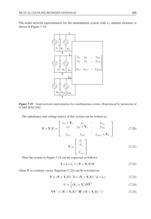
MUTUAL COUPLING BETWEEN ANTENNAS 193
The nodal network representation for the multiantenna system with nR antenna elements isshown in Figure 7.19:
YL1 iL1
I1
i1
YL2 iL2
I2
i2
YLnR iLnR
InR
inR
⎥⎥⎥⎥
⎦
⎤
⎢⎢⎢⎢
⎣
⎡
nRnRnRnR
nR
nR
yyy
yyy
yyy
,2,1,
,22221
,11211
...
...
...
Figure 7.19 Nodal network representation for a multiantenna system. (Reproduced by permission of© 2005 IEEE [49])
The admittance and voltage matrix of this system can be written as:
Y + YLU =
⎡⎢⎢⎣
y11 + YL y12 · y1nR
y21 y22 + YL · y2nR· · · ·ynR1 ynR2 · ynRnR
+ YL
⎤⎥⎥⎦ (7.20)
V =
⎡⎢⎢⎣
V1
V2
·VnR
⎤⎥⎥⎦ (7.21)
Thus the system in Figure 7.19 can be expressed as follows:
I = i + iL = (Y + YLU)V (7.22)
where U is a unitary vector. Equation (7.22) can be rewritten as:
V = (Y + YLU)−1I = (Y + YLU)−1(i + iL) (7.23)
N = 1
2(YL + Y∗
L)VV+ (7.24)
VV+ = (Y + YLU)−1II+((Y + YLU)−1)+ (7.25)
194 MULTIPLE ANTENNAS
where the symbol + indicates the Hermitian transpose and ∗ the complex conjugate. Then, thesquare of the current can be expressed as:
II+ = (i + iL) × (i + iL)+ (7.26)
Based on Equation (7.17) the following relations are valid and can be put into Equation (7.26):
1. ij i∗k= 2kT (yjk + y∗
jk)
2. iLj i∗k= 0 (7.27)
3. iLj i∗Lk
= 0, j = k
Finally, the square of the currents (7.26) is expressed as:
II+ = 2kT (Y + Y∗ + (YL + Y∗L)∗U) (7.28)
Substituting YL + Y∗L
= 2GL and Ya = Y + YLU, Equation (7.24) can be written as
N = 2kT GL
[Y−1
a× (Ya + Y∗
a) × (Y−1
a)+]
(7.29)
The thermal noise received in each antenna element includes two components, self- thermalnoise and induced thermal noise from the adjacent antenna elements. The total thermal noisepower received from the antenna array in the receiver load is given in Equation (7.29). Thetotal noise for two coupled antenna elements, in the frequency bandwidth B, can be simplifiedto be a sum of these noise powers:
Ntotal =∫
B
PL1df +∫
B
PL2df (7.30)
where PL1 is the thermal noise power absorbed in the receiver load of the first antenna, andPL2 is the thermal noise power absorbed in the receiver load of the second antenna.
To minimise mutual coupling between elements in a printed substrate, it is possible to createadditional isolation between antenna elements, such as designing slots as in Figure 7.19, oradding absorbing material. It is found that elements with better isolation can prevent thedistortion of the radiation pattern and thus increase the output gain [51].
References[1] Tolga M. Duman and Ali Ghrayeb, ‘Coding for MIMO Communication Systems’, John Wiley & Sons, Ltd,
Chichester, January 2008.[2] William Webb, ‘Wireless Communications: The Future’, John Wiley & Sons, Ltd, Chichester, March 2007.[3] Athos Kasapi, “http://www.bookfinder.com/dir/i/Smart_Antennas_and_Adaptive_Arrays-Multi-Antenna_
Techniques_for_Wireless/0750678097/ Smart Antennas and Adaptive Arrays: Multi-Antenna Techniques forWireless Communications’’ Butterworth-Heinemann Limited, ISBN 0750678097 (0-7506-7809-7), 2008.
[4] K. Huang and D. J. Edwards, ‘60 GHz Multi-beam Antenna Array for Gigabit Wireless CommunicationNetworks’, IEEE Transactions on Antennas and Propagation, 54(12), December 2006, 3912–3914.

REFERENCES 195
[5] M. Uno, Z. Wang, V. Wullich and K. Huang, ‘Communication System and Method’, Patents US2006116092,EP1659813 and JP2006148928, May 2006.
[6] S. Kobayashi, R. Mittra and R. Lampe, ‘Dielectric Tapered Rod Antenna for Millimetre Wave Applications’,IEEE Transactions on Antennas and Propagation, 30(1), January 1982, 54–58.
[7] J. Kraus and R. Marhefka, ‘Antennas for All Applications’, 3rd edition, McGraw-Hill, New York, 2002.[8] T. Ando, J. Yamauchi and H. Nakano, ‘Demonstration of the Discontinuity-Radiation Concept for a Dielectric
Rod Antenna’, Proceedings of IEEE Antennas and Propagation Society International Symposium, 16–21July2000, Vol. 2, pp. 856–859.
[9] K. Huang and Z. Wang, ‘V-Band Patch-Fed Rod Antennas for High Datarate Wireless Communications’, IEEETransactions on Antennas and Propagation, 54(1), January 2006, 297–300.
[10] K. Huang and Z. Wang, ‘Dielectric RodAntenna and Method for Operating theAntenna’, Patents WO2006097145and EP1703590, 21 September 2006.
[11] IEEE 802.15.3c Standard, http://www.ieee.org/[12] T. Ando, J. Yamauchi and H. Nakano, ‘Rectangular Dielectric-Rod by Metallic Waveguide’, IEE Proceedings
on Microwave, Antennas and Propagation, 149(2), April 2002, 92–97.[13] Kai Chang, ‘Phased Array Antennas’, John Wiley & Sons, Inc., New York, 2001.[14] David M. Pozar, ‘Considerations for Millimetre Wave Printed Antennas’, IEEE Transactions on Antennas and
Propagation, AP-31(5), September 1983, 740–747.[15] M. A. Weiss, ‘Microstrip Antennas for Millimetre Waves’, IEEE Transactions on Antennas and Propagation,
AP-29, January 1981, 171–174.[16] D. M. Pozar and D. H. Schaubert, ‘Comparison of Architectures for Monolithic Phased Array Antennas’,
Microwave Journal, 29, March 1986, 93–104.[17] J. R. James and C. M. Hall, ‘Investigation of New Concepts for Designing Millimetre-Wave Antennas’, Final
Technical Report on Contract DAJA37-80-C-0183, US Army European Research Office, September 1983.[18] P. B. Katehi and N. G.Alexopoulos, ‘On the Modeling of Electromagnetically Coupled MicrostripAntennas – The
Printed Strip Dipole’, IEEE Transactions on Antennas and Propagation, AP-32, November 1984, 1179–1186.[19] P. B. Katehi, N. G. Alexopoulos and I. Y. Hsia, ‘A Bandwidth Enhancement Method for Microstrip Antennas’,
IEEE Transactions on Antennas and Propagation, AP-35, January 1987, 5–12.[20] R. J. Mailloux, ‘Phased Array Antenna Handbook’, Artech House Inc, Norwood, Massachusetts, 2005.[21] R. J. Mailloux, ‘Phased Array Architecture’, IEEE Proceedings, 80(1), January 1992, 163–172.[22] A. K. Agrawal and E. L. Holzman, ‘Beamformer Architectures for Active Phased-Array Radar Antennas’, IEEE
Transactions on on Antennas and Propagation, AP-47(3), March 1999, 432–442.[23] B. Rama Rao, ‘94 GHz Slotted Waveguide Array Fabricated by Photolithographic Techniques’, Electronics
Letters, 20(4), 16 February 1984, 155–156.[24] H. Y. Yee, ‘Impedance of a Narrow Longitudinal Shunt Slot in a Slotted Waveguide Array’, IEEE Transactions
on Antennas and Propagation, AP-22, 1974, 589–592.[25] A. A. Oliner, ‘The Impedance Properties of Narrow Radiating Slots in the Broadface of Rectangular Waveguide’,
IEEE Transactions on Antennas and Propagation, AP-5, 1957, 12–20.[26] U. Kotthaus and B. Vowinkel, ‘Investigation of Planar for Submillimeter Receivers’, Transactions of the IEEE,
MTT-37, February 1989, 375–380.[27] G. M. Rebeiz and D. B. Rutledge, ‘Integrated Horn Antennas for Millimetre-Wave Applications’, Annals of
Telecommunications, 47, 1992, 38–48.[28] Y. Huang, ‘Integrated mm-Wave Planar Array Antenna with Low Loss Feeding Network’, World Patent WO
2006/097050 A1.[29] K. Noujeim and K. Balmain, ‘Fixed-Frequency Beam-Steerable Leaky-Wave Antennas’, PhD Dissertation,
Department of Electrical Computational Engineering, University of Toronto, Toronto, Ontario, Canada, 1998.[30] M. Guglielmi and A. A. Oliner, ‘A Practical Theory for Image Guide Leaky-Wave Antennas Loaded by Periodic
Metal Strips’, Proceedings of the 17th European Microwave Conference, Rome, Italy, 11–17 September 1987,pp. 549–554.
[31] A. A. Oliner, ‘Scannable Millimetre Wave Arrays’, Weber Research Institute, Polytechnic University, TechnicalReport Poly-WRI-1543-88, Vols I and 11, 30 September 1988.
[32] Limin Huang, Jung-Chih Chiao and Michael P. De Lisio, ‘An Electronically Switchable Leaky Wave Antenna’,IEEE Transactions on Antennas and Propagation, 48(11), November 2000, 1769–1772.
[33] Felix K. Schwering, ‘Millimetre Wave Antennas’, Proceedings of the IEEE, 80(1), January 1992, 92–102.

196 MULTIPLE ANTENNAS
[34] D. M. Pozar, ‘Input Impedance and Mutual Coupling of Rectangular Microstrip Antennas’, IEEE Transactionson Antennas and Propagation, AP-30, November 1982, 1191–1196.
[35] N. G.Alexopoulos and I. E. Rana, ‘Mutual Impedance Computation between Printed Dipoles’, IEEE Transactionson Antennas and Propagation, AP-29, January 1981, 110–111.
[36] R. F. Hamington, ‘Field Computation by Moment Methods’, Macmillan, New York, 1968.[37] Michael J. Gans, ‘Channel Capacity between Antenna Arrays – Part I: Sky Noise Dominates’, IEEE Transactions
on Communications, 54(9), September 2006, 1586–1592.[38] Michael J. Gans, ‘Channel Capacity between Antenna Arrays – Part II: Amplifier Noise Dominates’, IEEE
Transactions on Communications, 54(11), November 2006, 1983–1992.[39] I. J. Guptha and A. K. Ksienski, ‘Effect of the Mutual Coupling on the Performance of the Adaptive Arrays’,
IEEE Transactions on Antennas and Propagation, 31(5), 1983, 785–791.[40] W. Rotman, ‘EHF Dielectric Lens Antenna for Multibeam MIL-SATCOM Applications’ Digest of 1982
International IEEE-APSIURSI Symposium, Albuquerque, New Mexico, June 1982, pp. 132–135.[41] K. Iizuka, M. Mizusawa, S. Urasaki and J. Ushigome, ‘Volume-Type Holographic Antenna’, IEEE Transactions
on Antennas and Propagatation, AP-23, November 1975, 807–810.[42] P. Bhartia, K. V. S. Rao and R. S. Tomar, ‘Millimetre-Wave Microstrip and Printed Circuit Antennas’, Artech
House, London, 1991.[43] T. Sventenson and A. Ranheim, ‘Mutual Coupling Effects on the Capacity of the Multielement Antenna System’,
Proceedings of the International Conference on ‘Acoustic, Speech and Signal Processing’ (ICASSP’01), 2001.[44] J. W. Wallace and M. A. Jensen, ‘Mutual Coupling in MIMO Wireless Systems: A Rigorous Network Theory
Analysis’, IEEE Transactions on Wireless Communications, 3, 2004, 1317–1325.[45] S. Krusevac, P. Rapajic and R. Kennedy, ‘Method for MIMO Channel Capacity Estimation for Electro-
magnetically Coupled Transmit Antenna Elements’, AusCTW 2004 , February 2004, pp. 122–126.[46] S. M. Rytov, Yu. A. Krastov and V. I. Tatarskii, ‘Principles of Statistical Radiophysics 3 , Elements of the Random
Fields’, Springer, Berlin, Heidenberg, New York, 1987.[47] A. T. Starr, ‘Electric Circuit and Wave Filters’, 2nd edition, Pitman, London, 1946, p. 78.[48] S. Krusevac, P. B. Rapajic, R. A. Kennedy and P. Sadeghi, ‘Mutual Coupling Effect on Thermal Noise in
Multi-antenna Wireless Communication Systems’, Proceedings of the 6th Australian Communications TheoryWorkshop, February 2005, pp. 209–214.
[49] G. E. Vally and H. Wallman, ‘Vacuum Tube Amplifiers’, MIT Radio Laboratory Series 18, McGraw-Hill, Inc.,New York, 1949.
[50] R. Q. Twiss, ‘Nyquist’s and Thevenin’s Generalized for Nonreciprocal Linear Networks’, Journal of AppliedPhysics, 26, May 1955, 559–602.
[51] Y. Moon et al., ‘Flat-Plate MIMO Array Antenna with Isolation Element’, US Patent ApplicationUS2007/0069960.
8Smart Antennas
In an indoor environment, millimetre wave communications can have both line-of-sight andnon-line-of-sight wireless links [1], and it is difficult for an omnidirectional or fixed beamantenna to cope with both situations. A smart antenna system, which is an antenna arrayarranged in a special distributed configuration with a specialised signal processor, can bedeployed in a millimetre wave communication system to dynamically optimise the system’sperformance and capacity significantly by minimising undesired co-channel interference.Therefore, smart antennas are attractive as they can help to improve the millimetre wave com-munication quality. Various smart antenna technologies such as spatial diversity combining orbeamforming algorithms can be implemented to enhance the performance of a millimetre wavesystem. Most of the smart antenna systems published can form beams directed to a desiredsignal and form nulls towards an undesired interferer, such as a co-channel base station. Thisenhances the signal-to-interference (SIR) ratio because the received desired signal strength ismaximised and the undesired signal interference is minimised. The other benefits of a smartantenna are as follows:
• Increase in range or coverage arising from an increased signal strength due to array gain• Increase in capacity arising from interference rejection• Reject multipath interference arising from inherent spatial diversity of the array• Reducing expense arising from lower transmission powers to the intended end user
Smart antenna systems are commonly classified into several categories: mode tracking, beamswitching, beam steering/forming and multiple-input multiple-output. They can isolate aco-channel signal whereas multiple antennas cannot.
Abeam-switching antenna system consists of many highly directive, pre-defined fixed beamsformed with an antenna array. The system usually detects the maximum received signal strengthfrom the antenna beams, and chooses to transmit the output signal from one of the selectedbeams that gives the best performance. In many ways, a nine-beam switched antenna system isvery much like an extension of a sectoring directional antenna with multiple subsectors. Sincethe direction of the arrival information of the desired signal is not analysed, the desired signalmay not fall on to the maximum of the chosen beam because the direction of these beams is
Millimetre Wave Antennas for Gigabit Wireless Communications Kao-Cheng Huang and David J. Edwardsc© 2008 John Wiley & Sons, Ltd
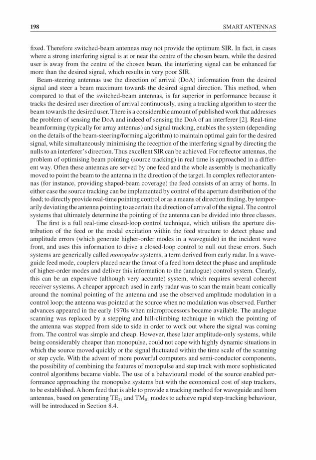
198 SMART ANTENNAS
fixed. Therefore switched-beam antennas may not provide the optimum SIR. In fact, in caseswhere a strong interfering signal is at or near the centre of the chosen beam, while the desireduser is away from the centre of the chosen beam, the interfering signal can be enhanced farmore than the desired signal, which results in very poor SIR.
Beam-steering antennas use the direction of arrival (DoA) information from the desiredsignal and steer a beam maximum towards the desired signal direction. This method, whencompared to that of the switched-beam antennas, is far superior in performance because ittracks the desired user direction of arrival continuously, using a tracking algorithm to steer thebeam towards the desired user. There is a considerable amount of published work that addressesthe problem of sensing the DoA and indeed of sensing the DoA of an interferer [2]. Real-timebeamforming (typically for array antennas) and signal tracking, enables the system (dependingon the details of the beam-steering/forming algorithm) to maintain optimal gain for the desiredsignal, while simultaneously minimising the reception of the interfering signal by directing thenulls to an interferer’s direction. Thus excellent SIR can be achieved. For reflector antennas, theproblem of optimising beam pointing (source tracking) in real time is approached in a differ-ent way. Often these antennas are served by one feed and the whole assembly is mechanicallymoved to point the beam to the antenna in the direction of the target. In complex reflector anten-nas (for instance, providing shaped-beam coverage) the feed consists of an array of horns. Ineither case the source tracking can be implemented by control of the aperture distribution of thefeed; to directly provide real-time pointing control or as a means of direction finding, by tempor-arily deviating the antenna pointing to ascertain the direction of arrival of the signal. The controlsystems that ultimately determine the pointing of the antenna can be divided into three classes.
The first is a full real-time closed-loop control technique, which utilises the aperture dis-tribution of the feed or the modal excitation within the feed structure to detect phase andamplitude errors (which generate higher-order modes in a waveguide) in the incident wavefront, and uses this information to drive a closed-loop control to null out these errors. Suchsystems are generically called monopulse systems, a term derived from early radar. In a wave-guide feed mode, couplers placed near the throat of a feed horn detect the phase and amplitudeof higher-order modes and deliver this information to the (analogue) control system. Clearly,this can be an expensive (although very accurate) system, which requires several coherentreceiver systems. A cheaper approach used in early radar was to scan the main beam conicallyaround the nominal pointing of the antenna and use the observed amplitude modulation in acontrol loop; the antenna was pointed at the source when no modulation was observed. Furtheradvances appeared in the early 1970s when microprocessors became available. The analoguescanning was replaced by a stepping and hill-climbing technique in which the pointing ofthe antenna was stepped from side to side in order to work out where the signal was comingfrom. The control was simple and cheap. However, these later amplitude-only systems, whilebeing considerably cheaper than monopulse, could not cope with highly dynamic situations inwhich the source moved quickly or the signal fluctuated within the time scale of the scanningor step cycle. With the advent of more powerful computers and semi-conductor components,the possibility of combining the features of monopulse and step track with more sophisticatedcontrol algorithms became viable. The use of a behavioural model of the source enabled per-formance approaching the monopulse systems but with the economical cost of step trackers,to be established. A horn feed that is able to provide a tracking method for waveguide and hornantennas, based on generating TE21 and TM01 modes to achieve rapid step-tracking behaviour,will be introduced in Section 8.4.
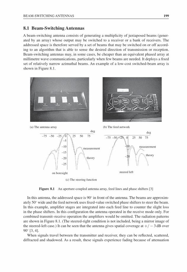
BEAM-SWITCHING ANTENNAS 199
8.1 Beam-Switching Antennas
A beam-switching antenna consists of generating a multiplicity of juxtaposed beams (gener-ated by an array) whose output may be switched to a receiver or a bank of receivers. Theaddressed space is therefore served by a set of beams that may be switched on or off accord-ing to an algorithm that is able to sense the desired direction of transmission or reception.Beam-switching antennas may, in some cases, be cheaper than an equivalent phased array atmillimetre wave communications, particularly when few beams are needed. It deploys a fixedset of relatively narrow azimuthal beams. An example of a low-cost switched-beam array isshown in Figure 8.1.
(a) The antenna array (b) The feed network
(c) The steering function
–75 –50 –25
–5
–10 –10
–20–15
–20
–25
0 25 50 75 –75 –50 –25 0 25 50 75
deg deg
measurement measurement
theorytheory
on boresight steered left
Figure 8.1 An aperture-coupled antenna array, feed lines and phase shifters [3]
In this antenna, the addressed space is 90◦ in front of the antenna. The beams are approxim-ately 50◦ wide and the feed network uses fixed-value switched phase shifters to steer the beam.In this example, amplifier stages are integrated into each feed line to counter the slight lossin the phase shifters. In this configuration the antenna operated in the receive mode only. Forcombined transmit–receive operation the amplifiers would be omitted. The radiation patternsare shown in Figure 8.1. (The steered-right condition is not included, being a mirror image ofthe steered-left case.) It can be seen that the antenna gives spatial coverage at +/ − 3 dB over90◦ [3, 4].
When signals travel between the transmitter and receiver, they can be reflected, scattered,diffracted and shadowed. As a result, these signals experience fading because of attenuation
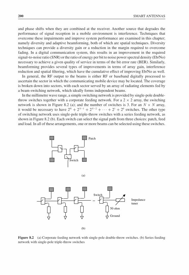
200 SMART ANTENNAS
and phase shifts when they are combined at the receiver. Another source that degrades theperformance of signal reception in a mobile environment is interference. Techniques thatovercome these impairments and improve system performance are examined in this chapter;namely diversity and adaptive beamforming, both of which are spatial techniques. Diversitytechniques can provide a diversity gain or a reduction in the margin required to overcomefading. In a digital communication system, this results in an improvement in the requiredsignal-to-noise ratio (SNR) or the ratio of energy per bit to noise power spectral density (Eb/No)necessary to achieve a given quality of service in terms of the bit error rate (BER). Similarly,beamforming provides several types of improvements in terms of array gain, interferencereduction and spatial filtering, which have the cumulative effect of improving Eb/No as well.
In general, the RF output to the beams is either RF or baseband digitally processed toascertain the sector in which the communicating mobile device may be located. The coverageis broken down into sectors, with each sector served by an array of radiating elements fed bya beam-switching network, which ideally forms independent beams.
In the millimetre wave range, a simple switching network is provided by single-pole double-throw switches together with a corporate feeding network. For a 2 × 2 array, the switchingnetwork is shown in Figure 8.2 (a); and the number of switches is 3. For an N × N array,it would be necessary to have 2N + 2N−1 + 2N−2 + · · · + 21 + 20 switches. The other typeof switching network uses single-pole triple-throw switches with a series feeding network, asshown in Figure 8.2 (b). Each switch can select the signal path from three choices: patch, feedand load. In all of these arrangements, one or more beams can be selected using these switches.
(a)
(b)
...
50 ohm
Ground
Impedance tuner
Switch
Switch
Patch
Figure 8.2 (a) Corporate feeding network with single-pole double-throw switches. (b) Series feedingnetwork with single-pole triple-throw switches
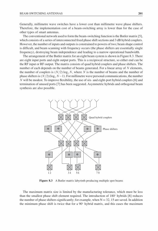
BEAM-SWITCHING ANTENNAS 201
Generally, millimetre wave switches have a lower cost than millimetre wave phase shifters.Therefore, the implementation cost of a beam-switching array is lower than for the case ofother types of smart antennas.
The conventional network used to form the beam-switching function is the Butler matrix [5],which consists of a series of interconnected fixed phase shift sections and 3 dB hybrid couplers.However, the number of inputs and outputs is constrained to powers of two; beam shape controlis difficult, and beam scanning with frequency occurs (the phase shifters are essentially singlefrequency), destroying beam independence and leading to a narrow operational bandwidth.
The arrangement of the Butler matrix for an eight beam system is shown in Figure 8.3. Thereare eight input ports and eight output ports. This is a reciprocal structure, so either end can bethe RF input or RF output. The matrix consists of quad hybrid couplers and phase shifters. Thenumber of each depends on the number of beams generated. For a linear array of N elements,the number of couplers is (N/2) log2 N , where N is the number of beams and the number ofphase shifters is (N/2)(log2 N−1). For millimetre wave personal communications, the numberN will be modest. To improve flexibility, the use of six- and eight-port hybrid couplers [6] andtermination of unused ports [7] has been suggested. Asymmetric hybrids and orthogonal beamsynthesis are also possible.
531 2 4 6 7 8
Phase shifters
Quad hybrid couplers
Φ
Φ
Φ Φ Φ
Φ Φ Φ
Figure 8.3 A Butler matrix labyrinth producing multiple spot beams
The maximum matrix size is limited by the manufacturing tolerance, which must be lessthan the smallest phase shift element required. The introduction of 180◦ hybrids [8] reducesthe number of phase shifters significantly; for example, when N = 32, 15 are saved. In additionthe minimum phase shift is twice that for a 90◦ hybrid matrix, and this eases the maximum
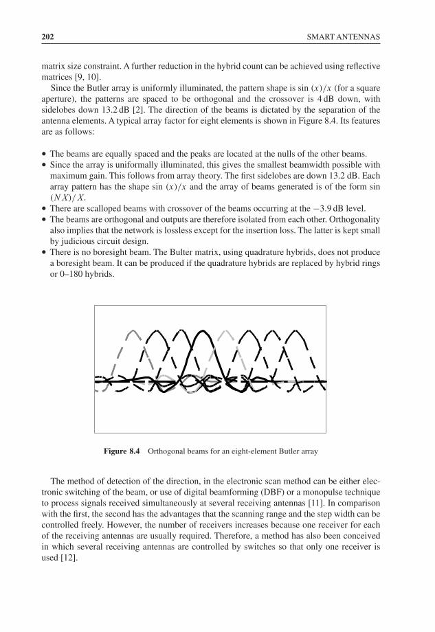
202 SMART ANTENNAS
matrix size constraint. A further reduction in the hybrid count can be achieved using reflectivematrices [9, 10].
Since the Butler array is uniformly illuminated, the pattern shape is sin (x)/x (for a squareaperture), the patterns are spaced to be orthogonal and the crossover is 4 dB down, withsidelobes down 13.2 dB [2]. The direction of the beams is dictated by the separation of theantenna elements. A typical array factor for eight elements is shown in Figure 8.4. Its featuresare as follows:
• The beams are equally spaced and the peaks are located at the nulls of the other beams.• Since the array is uniformally illuminated, this gives the smallest beamwidth possible with
maximum gain. This follows from array theory. The first sidelobes are down 13.2 dB. Eacharray pattern has the shape sin (x)/x and the array of beams generated is of the form sin(NX)/X.
• There are scalloped beams with crossover of the beams occurring at the −3.9 dB level.• The beams are orthogonal and outputs are therefore isolated from each other. Orthogonality
also implies that the network is lossless except for the insertion loss. The latter is kept smallby judicious circuit design.
• There is no boresight beam. The Bulter matrix, using quadrature hybrids, does not producea boresight beam. It can be produced if the quadrature hybrids are replaced by hybrid ringsor 0–180 hybrids.
Figure 8.4 Orthogonal beams for an eight-element Butler array
The method of detection of the direction, in the electronic scan method can be either elec-tronic switching of the beam, or use of digital beamforming (DBF) or a monopulse techniqueto process signals received simultaneously at several receiving antennas [11]. In comparisonwith the first, the second has the advantages that the scanning range and the step width can becontrolled freely. However, the number of receivers increases because one receiver for eachof the receiving antennas are usually required. Therefore, a method has also been conceivedin which several receiving antennas are controlled by switches so that only one receiver isused [12].
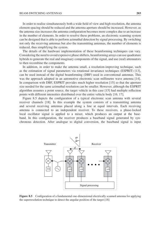
BEAM-SWITCHING ANTENNAS 203
In order to realise simultaneously both a wide field of view and high resolution, the antennaelement spacing should be reduced and the antenna aperture should be increased. However, asthe antenna size increases the antenna configuration becomes more complex due to an increasein the number of elements. In order to resolve these problems, an electronic scanning systemcan be designed that is able to perform azimuthal detection by signal processing. By switchingnot only the receiving antennas but also the transmitting antennas, the number of elements isreduced, thus simplifying the system.
The details of the hardware implementation of these beamforming techniques can vary.Considering the need to avoid expensive phase shifters, beamforming arrays can use quadraturehybrids to generate the real and imaginary components of the signal, and use (real) attenuatorsto then recombine the components.
In addition, in order to make the antenna small, a resolution-improving technique, suchas the estimation of signal parameters via rotational invariance techniques (ESPRIT) [13],can be used instead of the digital beamforming (DBF) used in conventional antennas. Thiswas the approach adopted in an automotive electronic scan millimetre wave antenna [14].In comparison with DBF, ESPRIT provides much higher resolution [15] so that the aperturesize needed for the same azimuthal resolution can be smaller. However, although the ESPRITalgorithm assumes a point source, the target vehicle in this case [15] had multiple reflectionpoints with different intensities distributed over the entire vehicle body [16, 17].
Figure 8.5 depicts the configuration of a typical electronic scan antenna with severalreceiver channels [18]. In this example the system consists of a transmitting antennaand several receiving antennas placed along a line at equal intervals. Each receivingantenna is connected to an independent receiver. To these receivers, a phase-lockedlocal oscillator signal is applied to a mixer, which produces an output at the base-band. In this configuration, the receiver produces a baseband signal generated by syn-chronous detection. After analogue to digital conversion, the baseband signal is input
A/D A/D A/D
Signal processing
ReceiverTransmitter
D/A
d
θ
Figure 8.5 Configuration of a fundamental one-dimensional electrically scanned antenna for applyingthe superresolution technique to detect the angular position of the target [18]
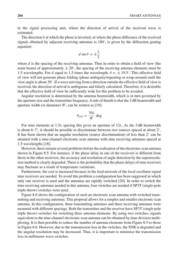
204 SMART ANTENNAS
to the signal processing unit, where the direction of arrival of the received wave isestimated.
The direction θ at which the phase is inverted, or where the phase difference of the receivedsignals obtained by adjacent receiving antennas is 180◦, is given by the diffraction gratingequation:
d sin θ = ±λ
2
where d is the spacing of the receiving antennas. Thus in order to obtain a field of view (themain beam) of approximately ± 20◦, the spacing of the receiving antenna elements must be1.5 wavelengths. For d equal to 1.5 times the wavelength, θ = ± 19.5◦. This effective fieldof view will not generate phase folding (phase ambiguity/repeating or wrap-around) until theview angle is about 39◦. If a wave arriving from a direction outside the effective field of view isreceived, the direction of arrival is ambiguous and falsely calculated. Therefore, it is desirablethat the effective field of view be sufficiently wide for this problem to be avoided.
Angular resolution is determined by the antenna beamwidth, which is in turn governed bythe aperture size and the transmitter frequency. A rule of thumb is that the 3 dB beamwidth andaperture width (or diameter) W , can be written as [19]:
θ3dB = 70λ
Wdeg
For nine elements at 1.5λ spacing this gives an aperture of 12λ. As the 3 dB beamwidthis about 6–7◦, it should be possible to discriminate between two sources spaced at about 2◦.It has been shown that an angular resolution (source discrimination) of less than 2◦ can beattained with a nine-channel electronic scan antenna with nine receiving antennas spaced at1.5 wavelengths [18].
However, there remain several problems before the realisation of the electronic scan antennashown in Figure 8.5. For instance, if the phase delay in one of the receivers is different fromthose in the other receivers, the accuracy and resolution of angle detection by the superresolu-tion method is clearly degraded. There is the probability that the phase delays of nine receiversmay fluctuate as a result of temperature variations.
Furthermore, the cost is increased because in the feed network of the local oscillator signalnine receivers are needed. To avoid this problem a configuration has been suggested in whichonly one receiver is used and the antennas are rapidly switched [20]. In order to switch thenine receiving antennas needed in this antenna, four switches are needed if SP3T (single-poletriple-throw) switches were used.
Figure 8.6 shows the configuration of such an electronic scan antenna with switched trans-mitting and receiving antennas. This proposal allows for a simpler and smaller electronic scanantenna. In this configuration, three transmitting antennas and three receiving antennas weremounted with different spacings. Both the transmitter and the receiver have SP3T (single poletriple throw) switches for switching three antenna elements. By using two switches, signalsequivalent to the nine-channel electronic scan antenna can be obtained by time division multi-plexing. It is then possible to reduce the number of antenna elements from Figure 8.5 to thosein Figure 8.6. However, due to the transmission loss in the switches, the SNR is degraded andthe angular resolution may be decreased. Thus, it is important to minimise the transmissionloss in millimetre wave switches.
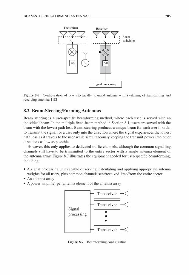
BEAM-STEERING/FORMING ANTENNAS 205
A/D
Signal processing
ReceiverTransmitter
Beamswitching
D/A
Figure 8.6 Configuration of new electrically scanned antenna with switching of transmitting andreceiving antennas [18]
8.2 Beam-Steering/Forming Antennas
Beam steering is a user-specific beamforming method, where each user is served with anindividual beam. In the multiple fixed-beam method in Section 8.1, users are served with thebeam with the lowest path loss. Beam steering produces a unique beam for each user in orderto transmit the signal for a user only into the direction where the signal experiences the lowestpath loss as it travels to the user while simultaneously keeping the transmit power into otherdirections as low as possible.
However, this only applies to dedicated traffic channels, although the common signallingchannels still have to be transmitted to the entire sector with a single antenna element ofthe antenna array. Figure 8.7 illustrates the equipment needed for user-specific beamforming,including:
• A signal processing unit capable of serving, calculating and applying appropriate antennaweights for all users, plus common channels sent/received, into/from the entire sector
• An antenna array• A power amplifier per antenna element of the antenna array
Transceiver
Transceiver
Transceiver
Signalprocessing
Figure 8.7 Beamforming configuration
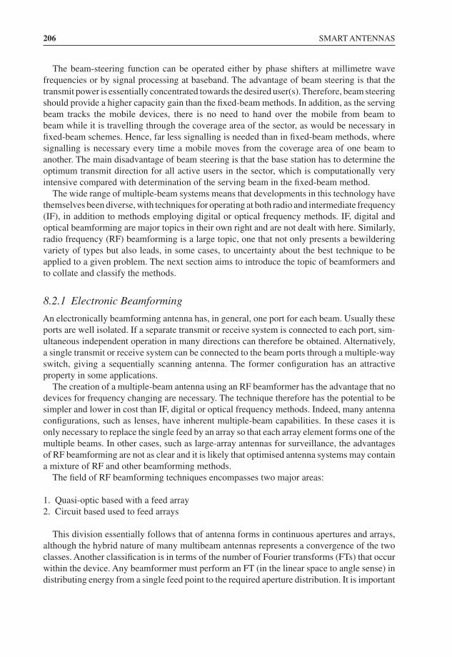
206 SMART ANTENNAS
The beam-steering function can be operated either by phase shifters at millimetre wavefrequencies or by signal processing at baseband. The advantage of beam steering is that thetransmit power is essentially concentrated towards the desired user(s). Therefore, beam steeringshould provide a higher capacity gain than the fixed-beam methods. In addition, as the servingbeam tracks the mobile devices, there is no need to hand over the mobile from beam tobeam while it is travelling through the coverage area of the sector, as would be necessary infixed-beam schemes. Hence, far less signalling is needed than in fixed-beam methods, wheresignalling is necessary every time a mobile moves from the coverage area of one beam toanother. The main disadvantage of beam steering is that the base station has to determine theoptimum transmit direction for all active users in the sector, which is computationally veryintensive compared with determination of the serving beam in the fixed-beam method.
The wide range of multiple-beam systems means that developments in this technology havethemselves been diverse, with techniques for operating at both radio and intermediate frequency(IF), in addition to methods employing digital or optical frequency methods. IF, digital andoptical beamforming are major topics in their own right and are not dealt with here. Similarly,radio frequency (RF) beamforming is a large topic, one that not only presents a bewilderingvariety of types but also leads, in some cases, to uncertainty about the best technique to beapplied to a given problem. The next section aims to introduce the topic of beamformers andto collate and classify the methods.
8.2.1 Electronic Beamforming
An electronically beamforming antenna has, in general, one port for each beam. Usually theseports are well isolated. If a separate transmit or receive system is connected to each port, sim-ultaneous independent operation in many directions can therefore be obtained. Alternatively,a single transmit or receive system can be connected to the beam ports through a multiple-wayswitch, giving a sequentially scanning antenna. The former configuration has an attractiveproperty in some applications.
The creation of a multiple-beam antenna using an RF beamformer has the advantage that nodevices for frequency changing are necessary. The technique therefore has the potential to besimpler and lower in cost than IF, digital or optical frequency methods. Indeed, many antennaconfigurations, such as lenses, have inherent multiple-beam capabilities. In these cases it isonly necessary to replace the single feed by an array so that each array element forms one of themultiple beams. In other cases, such as large-array antennas for surveillance, the advantagesof RF beamforming are not as clear and it is likely that optimised antenna systems may containa mixture of RF and other beamforming methods.
The field of RF beamforming techniques encompasses two major areas:
1. Quasi-optic based with a feed array2. Circuit based used to feed arrays
This division essentially follows that of antenna forms in continuous apertures and arrays,although the hybrid nature of many multibeam antennas represents a convergence of the twoclasses. Another classification is in terms of the number of Fourier transforms (FTs) that occurwithin the device. Any beamformer must perform an FT (in the linear space to angle sense) indistributing energy from a single feed point to the required aperture distribution. It is important
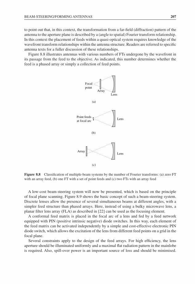
BEAM-STEERING/FORMING ANTENNAS 207
to point out that, in this context, the transformation from a far-field (diffraction) pattern of theantenna to the aperture plane is described by a (angle to spatial) Fourier transform relationship.In this context the placement of feeds within a quasi-optical system requires knowledge of thewavefront transform relationships within the antenna structure. Readers are referred to specificantenna texts for a fuller discussion of these relationships.
Figure 8.8 illustrates antennas with various numbers of FTs undergone by the wavefront inits passage from the feed to the objective. As indicated, this number determines whether thefeed is a phased array or simply a collection of feed points.
(a)
(b)
(c)
LensArray
Focalpoint
LensPoint feeds at focal arc
ArrayLens
Figure 8.8 Classification of multiple-beam systems by the number of Fourier transforms: (a) zero FTwith an array feed, (b) one FT with a set of point feeds and (c) two FTs with an array feed
A low-cost beam-steering system will now be presented, which is based on the principleof focal plane scanning. Figure 8.9 shows the basic concept of such a beam-steering system.Discrete lenses allow the presence of several simultaneous beams at different angles, with asimpler feed structure than phased arrays. Here, instead of using a bulky microwave lens, aplanar filter lens array (FLA) as described in [22] can be used as the focusing element.
A conformal feed matrix is placed in the focal arc of a lens and fed by a feed networkequipped with PIN (positive intrinsic negative) diode switches. In this way, each element ofthe feed matrix can be activated independently by a simple and cost-effective electronic PINdiode switch, which allows the excitation of the lens from different feed points on a grid in thefocal plane.
Several constraints apply to the design of the feed arrays. For high efficiency, the lensaperture should be illuminated uniformly and a maximal flat radiation pattern in the mainlobeis required. Also, spill-over power is an important source of loss and should be minimised.
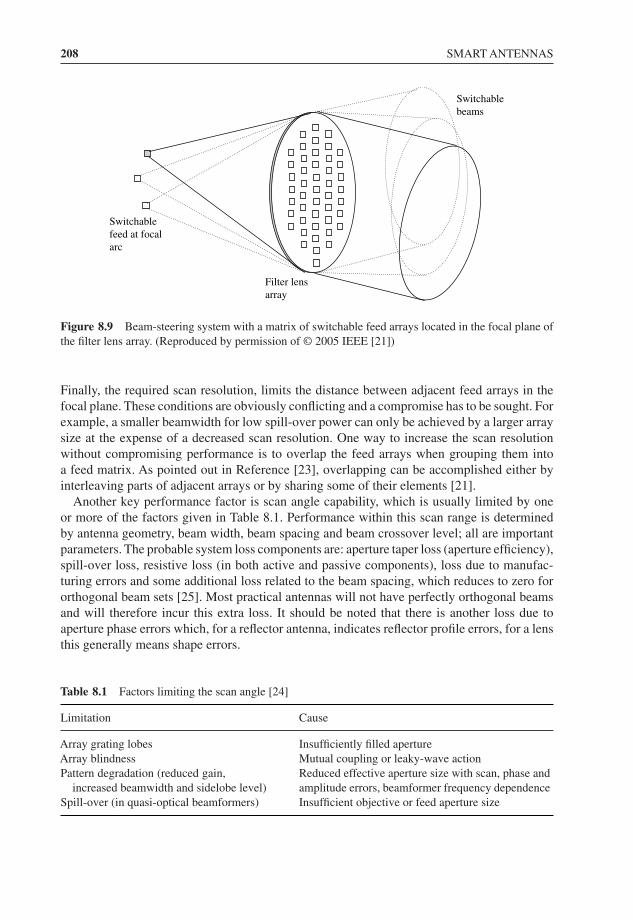
208 SMART ANTENNAS
Filter lensarray
Switchablefeed at focalarc
Switchablebeams
Figure 8.9 Beam-steering system with a matrix of switchable feed arrays located in the focal plane ofthe filter lens array. (Reproduced by permission of © 2005 IEEE [21])
Finally, the required scan resolution, limits the distance between adjacent feed arrays in thefocal plane. These conditions are obviously conflicting and a compromise has to be sought. Forexample, a smaller beamwidth for low spill-over power can only be achieved by a larger arraysize at the expense of a decreased scan resolution. One way to increase the scan resolutionwithout compromising performance is to overlap the feed arrays when grouping them intoa feed matrix. As pointed out in Reference [23], overlapping can be accomplished either byinterleaving parts of adjacent arrays or by sharing some of their elements [21].
Another key performance factor is scan angle capability, which is usually limited by oneor more of the factors given in Table 8.1. Performance within this scan range is determinedby antenna geometry, beam width, beam spacing and beam crossover level; all are importantparameters. The probable system loss components are: aperture taper loss (aperture efficiency),spill-over loss, resistive loss (in both active and passive components), loss due to manufac-turing errors and some additional loss related to the beam spacing, which reduces to zero fororthogonal beam sets [25]. Most practical antennas will not have perfectly orthogonal beamsand will therefore incur this extra loss. It should be noted that there is another loss due toaperture phase errors which, for a reflector antenna, indicates reflector profile errors, for a lensthis generally means shape errors.
Table 8.1 Factors limiting the scan angle [24]
Limitation Cause
Array grating lobes Insufficiently filled apertureArray blindness Mutual coupling or leaky-wave actionPattern degradation (reduced gain,
increased beamwidth and sidelobe level)Reduced effective aperture size with scan, phase andamplitude errors, beamformer frequency dependence
Spill-over (in quasi-optical beamformers) Insufficient objective or feed aperture size
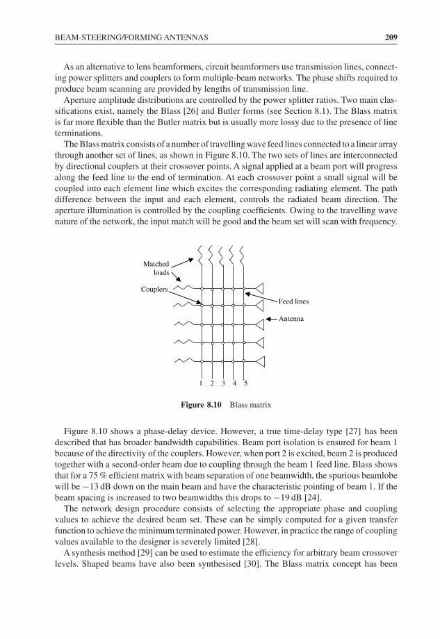
BEAM-STEERING/FORMING ANTENNAS 209
As an alternative to lens beamformers, circuit beamformers use transmission lines, connect-ing power splitters and couplers to form multiple-beam networks. The phase shifts required toproduce beam scanning are provided by lengths of transmission line.
Aperture amplitude distributions are controlled by the power splitter ratios. Two main clas-sifications exist, namely the Blass [26] and Butler forms (see Section 8.1). The Blass matrixis far more flexible than the Butler matrix but is usually more lossy due to the presence of lineterminations.
The Blass matrix consists of a number of travelling wave feed lines connected to a linear arraythrough another set of lines, as shown in Figure 8.10. The two sets of lines are interconnectedby directional couplers at their crossover points. A signal applied at a beam port will progressalong the feed line to the end of termination. At each crossover point a small signal will becoupled into each element line which excites the corresponding radiating element. The pathdifference between the input and each element, controls the radiated beam direction. Theaperture illumination is controlled by the coupling coefficients. Owing to the travelling wavenature of the network, the input match will be good and the beam set will scan with frequency.
1 2 3 4 5
Feed lines
Antenna
Matched loads
Couplers
Figure 8.10 Blass matrix
Figure 8.10 shows a phase-delay device. However, a true time-delay type [27] has beendescribed that has broader bandwidth capabilities. Beam port isolation is ensured for beam 1because of the directivity of the couplers. However, when port 2 is excited, beam 2 is producedtogether with a second-order beam due to coupling through the beam 1 feed line. Blass showsthat for a 75 % efficient matrix with beam separation of one beamwidth, the spurious beamlobewill be −13 dB down on the main beam and have the characteristic pointing of beam 1. If thebeam spacing is increased to two beamwidths this drops to −19 dB [24].
The network design procedure consists of selecting the appropriate phase and couplingvalues to achieve the desired beam set. These can be simply computed for a given transferfunction to achieve the minimum terminated power. However, in practice the range of couplingvalues available to the designer is severely limited [28].
A synthesis method [29] can be used to estimate the efficiency for arbitrary beam crossoverlevels. Shaped beams have also been synthesised [30]. The Blass matrix concept has been
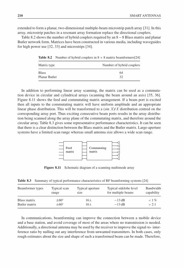
210 SMART ANTENNAS
extended to form a planar, two-dimensional multiple-beam microstrip patch array [31]. In thisarray, microstrip patches in a resonant array formation replace the directional couplers.
Table 8.2 shows the number of hybrid couplers required by an 8−8 Blass matrix and planarButler network form. Matrices have been constructed in various media, including waveguidesfor high power use [32, 33] and microstrips [34].
Table 8.2 Number of hybrid couplers in 8 × 8 matrix beamformers[24]
Matrix type Number of hybrid couplers
Blass 64Planar Butler 32
In addition to performing linear array scanning, the matrix can be used as a commuta-tion device in circular and cylindrical arrays (scanning the beam around an axis) [35, 36].Figure 8.11 shows the feed and commutating matrix arrangement. If a beam port is excitedthen all inputs to the commutating matrix will have uniform amplitude and an appropriatelinear phase distribution. This will be transformed to a (sin X)/X distribution centred on thecorresponding array port. Thus exciting consecutive beam ports results in the array distribu-tion being scanned along the array plane of the commutating matrix, and therefore around thecircular array. Table 8.3 gives some representative performance characteristics. It can be seenthat there is a clear distinction between the Blass matrix and the Butler matrix. Large-aperturesystems have a limited scan range whereas small antenna size allows a wide scan range.
Feedmatrix
Commutating matrix
Figure 8.11 Schematic diagram of a scanning multimode array
Table 8.3 Summary of typical performance characteristics of RF beamforming systems [24]
Beamformer types Typical scanrange
Typical aperturesize
Typical sidelobe levelfor multiple beams
Bandwidthcapability
Blass matrix ±60◦ 16 λ −13 dB < 1 %Butler matrix ±60◦ 16 λ −13 dB > 2:1
In communications, beamforming can improve the connection between a mobile deviceand a base station, and avoid coverage of most of the areas where no transmission is needed.Additionally, a directional antenna may be used by the receiver to improve the signal-to- inter-ference ratio by nulling out any interference from unwanted transmitters. In both cases, onlyrough estimates about the size and shape of such a transformed beam can be made. Therefore,
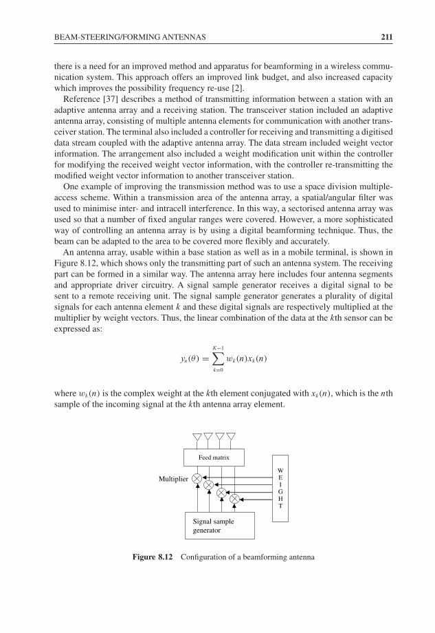
BEAM-STEERING/FORMING ANTENNAS 211
there is a need for an improved method and apparatus for beamforming in a wireless commu-nication system. This approach offers an improved link budget, and also increased capacitywhich improves the possibility frequency re-use [2].
Reference [37] describes a method of transmitting information between a station with anadaptive antenna array and a receiving station. The transceiver station included an adaptiveantenna array, consisting of multiple antenna elements for communication with another trans-ceiver station. The terminal also included a controller for receiving and transmitting a digitiseddata stream coupled with the adaptive antenna array. The data stream included weight vectorinformation. The arrangement also included a weight modification unit within the controllerfor modifying the received weight vector information, with the controller re-transmitting themodified weight vector information to another transceiver station.
One example of improving the transmission method was to use a space division multiple-access scheme. Within a transmission area of the antenna array, a spatial/angular filter wasused to minimise inter- and intracell interference. In this way, a sectorised antenna array wasused so that a number of fixed angular ranges were covered. However, a more sophisticatedway of controlling an antenna array is by using a digital beamforming technique. Thus, thebeam can be adapted to the area to be covered more flexibly and accurately.
An antenna array, usable within a base station as well as in a mobile terminal, is shown inFigure 8.12, which shows only the transmitting part of such an antenna system. The receivingpart can be formed in a similar way. The antenna array here includes four antenna segmentsand appropriate driver circuitry. A signal sample generator receives a digital signal to besent to a remote receiving unit. The signal sample generator generates a plurality of digitalsignals for each antenna element k and these digital signals are respectively multiplied at themultiplier by weight vectors. Thus, the linear combination of the data at the kth sensor can beexpressed as:
yn(θ) =K−1∑k=0
wk(n)xk(n)
where wk(n) is the complex weight at the kth element conjugated with xk(n), which is the nthsample of the incoming signal at the kth antenna array element.
Feed matrix
Signal samplegenerator
WEIGHT
Multiplier
Figure 8.12 Configuration of a beamforming antenna
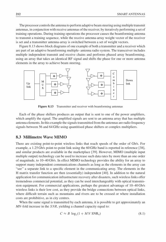
212 SMART ANTENNAS
The processor controls the antenna to perform adaptive beam steering using multiple transmitantennas, in conjunction with receive antennas of the receiver, by iteratively performing a set oftraining operations. During training operations the processor causes the beamforming antennato transmit a training sequence, while the receive antenna-array weight vector of the receiveris set and a transmitter antenna-array is switched between a set of weight vectors.
Figure 8.13 shows block diagrams of one example of both a transmitter and a receiver whichare part of an adaptive beamforming multiple- antenna radio system. The transceiver includesmultiple independent transmit and receive chains and performs phased array beamforming,using an array that takes an identical RF signal and shifts the phase for one or more antennaelements in the array to achieve beam steering.
Φ
Φ
Φ
MUX
ΦCombiner
Φ
Φ
DownlinkUp
link
Figure 8.13 Transmitter and receiver with beamforming antennas
Each of the phase shifters produces an output that is sent to one of the power amplifiers,which amplify the signal. The amplified signals are sent to an antenna array that has multipleantenna elements. In this example the signals transmitted from the antennas are radio frequencysignals between 56 and 64 GHz using quantitised phase shifters or complex multipliers.
8.3 Millimetre Wave MIMO
There are existing point-to-point wireless links that reach speeds of the order of Gb/s. Forexample, a 1.25 Gb/s point-to-point link using the 60 GHz band is reported in reference [38],and similar products are available in the marketplace [39]. However, MIMO (multiple inputmultiple output) technology can be used to increase such data rates by more than an one orderof magnitude, to 10–40 Gb/s. In effect MIMO technology provides the ability for an array tosupport many independent communications channels as long as the elements in the array can“see’’ a separate link to a specific element in the communicating array. The elements in theH matrix transfer function are then (essentially) independent [40]. In addition to the naturalapplication for communication infrastructure recovery after disasters, such wireless links offertremendous commercial potential, as they can be used interchangeably with optical transmis-sion equipment. For commercial applications, perhaps the greatest advantage of 10–40 Gb/swireless links is their low cost, as they provide the bridge connections between optical links,where difficult terrain such as mountains and rivers are to be crossed or where installationcosts are prohibitive, as in city centres.
When the same signal is transmitted by each antenna, it is possible to get approximately anMN-fold increase in the SNR, yielding a channel capacity equal to:
C ≈ B log2(1 + MN SNR0) (8.1)
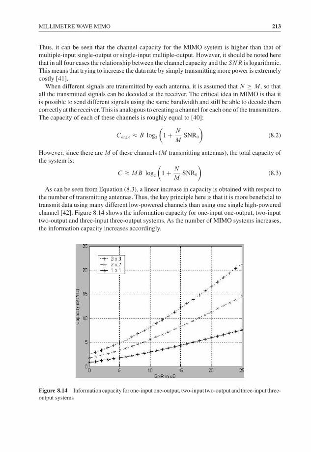
MILLIMETRE WAVE MIMO 213
Thus, it can be seen that the channel capacity for the MIMO system is higher than that ofmultiple-input single-output or single-input multiple-output. However, it should be noted herethat in all four cases the relationship between the channel capacity and the SNR is logarithmic.This means that trying to increase the data rate by simply transmitting more power is extremelycostly [41].
When different signals are transmitted by each antenna, it is assumed that N ≥ M , so thatall the transmitted signals can be decoded at the receiver. The critical idea in MIMO is that itis possible to send different signals using the same bandwidth and still be able to decode themcorrectly at the receiver. This is analogous to creating a channel for each one of the transmitters.The capacity of each of these channels is roughly equal to [40]:
Csingle ≈ B log2
(1 + N
MSNR0
)(8.2)
However, since there are M of these channels (M transmitting antennas), the total capacity ofthe system is:
C ≈ MB log2
(1 + N
MSNR0
)(8.3)
As can be seen from Equation (8.3), a linear increase in capacity is obtained with respect tothe number of transmitting antennas. Thus, the key principle here is that it is more beneficial totransmit data using many different low-powered channels than using one single high-poweredchannel [42]. Figure 8.14 shows the information capacity for one-input one-output, two-inputtwo-output and three-input three-output systems. As the number of MIMO systems increases,the information capacity increases accordingly.
Figure 8.14 Information capacity for one-input one-output, two-input two-output and three-input three-output systems
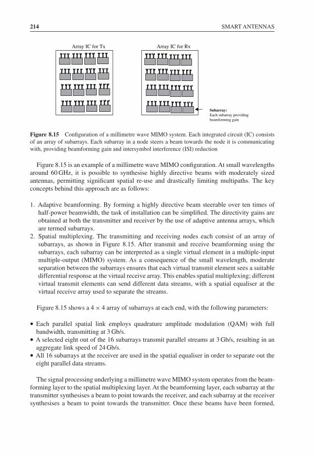
214 SMART ANTENNAS
Array IC for Tx
Subarray:Each subarray providingbeamforming gain
Array IC for Rx
Figure 8.15 Configuration of a millimetre wave MIMO system. Each integrated circuit (IC) consistsof an array of subarrays. Each subarray in a node steers a beam towards the node it is communicatingwith, providing beamforming gain and intersymbol interference (ISI) reduction
Figure 8.15 is an example of a millimetre wave MIMO configuration. At small wavelengthsaround 60 GHz, it is possible to synthesise highly directive beams with moderately sizedantennas, permitting significant spatial re-use and drastically limiting multipaths. The keyconcepts behind this approach are as follows:
1. Adaptive beamforming. By forming a highly directive beam steerable over ten times ofhalf-power beamwidth, the task of installation can be simplified. The directivity gains areobtained at both the transmitter and receiver by the use of adaptive antenna arrays, whichare termed subarrays.
2. Spatial multiplexing. The transmitting and receiving nodes each consist of an array ofsubarrays, as shown in Figure 8.15. After transmit and receive beamforming using thesubarrays, each subarray can be interpreted as a single virtual element in a multiple-inputmultiple-output (MIMO) system. As a consequence of the small wavelength, moderateseparation between the subarrays ensures that each virtual transmit element sees a suitabledifferential response at the virtual receive array. This enables spatial multiplexing; differentvirtual transmit elements can send different data streams, with a spatial equaliser at thevirtual receive array used to separate the streams.
Figure 8.15 shows a 4 × 4 array of subarrays at each end, with the following parameters:
• Each parallel spatial link employs quadrature amplitude modulation (QAM) with fullbandwidth, transmitting at 3 Gb/s.
• A selected eight out of the 16 subarrays transmit parallel streams at 3 Gb/s, resulting in anaggregate link speed of 24 Gb/s.
• All 16 subarrays at the receiver are used in the spatial equaliser in order to separate out theeight parallel data streams.
The signal processing underlying a millimetre wave MIMO system operates from the beam-forming layer to the spatial multiplexing layer. At the beamforming layer, each subarray at thetransmitter synthesises a beam to point towards the receiver, and each subarray at the receiversynthesises a beam to point towards the transmitter. Once these beams have been formed,
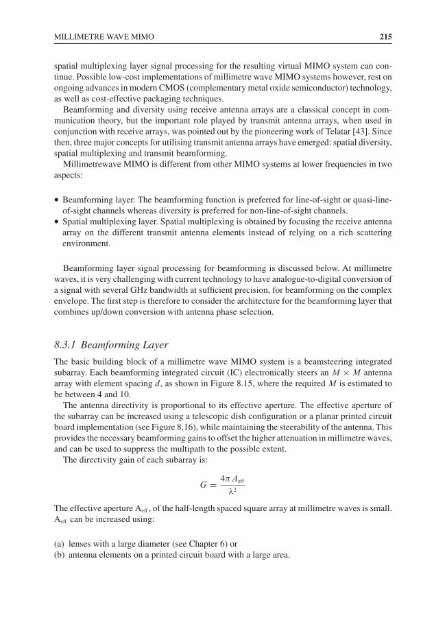
MILLIMETRE WAVE MIMO 215
spatial multiplexing layer signal processing for the resulting virtual MIMO system can con-tinue. Possible low-cost implementations of millimetre wave MIMO systems however, rest onongoing advances in modern CMOS (complementary metal oxide semiconductor) technology,as well as cost-effective packaging techniques.
Beamforming and diversity using receive antenna arrays are a classical concept in com-munication theory, but the important role played by transmit antenna arrays, when used inconjunction with receive arrays, was pointed out by the pioneering work of Telatar [43]. Sincethen, three major concepts for utilising transmit antenna arrays have emerged: spatial diversity,spatial multiplexing and transmit beamforming.
Millimetrewave MIMO is different from other MIMO systems at lower frequencies in twoaspects:
• Beamforming layer. The beamforming function is preferred for line-of-sight or quasi-line-of-sight channels whereas diversity is preferred for non-line-of-sight channels.
• Spatial multiplexing layer. Spatial multiplexing is obtained by focusing the receive antennaarray on the different transmit antenna elements instead of relying on a rich scatteringenvironment.
Beamforming layer signal processing for beamforming is discussed below. At millimetrewaves, it is very challenging with current technology to have analogue-to-digital conversion ofa signal with several GHz bandwidth at sufficient precision, for beamforming on the complexenvelope. The first step is therefore to consider the architecture for the beamforming layer thatcombines up/down conversion with antenna phase selection.
8.3.1 Beamforming Layer
The basic building block of a millimetre wave MIMO system is a beamsteering integratedsubarray. Each beamforming integrated circuit (IC) electronically steers an M × M antennaarray with element spacing d , as shown in Figure 8.15, where the required M is estimated tobe between 4 and 10.
The antenna directivity is proportional to its effective aperture. The effective aperture ofthe subarray can be increased using a telescopic dish configuration or a planar printed circuitboard implementation (see Figure 8.16), while maintaining the steerability of the antenna. Thisprovides the necessary beamforming gains to offset the higher attenuation in millimetre waves,and can be used to suppress the multipath to the possible extent.
The directivity gain of each subarray is:
G = 4πAeff
λ2
The effective aperture Aeff , of the half-length spaced square array at millimetre waves is small.Aeff can be increased using:
(a) lenses with a large diameter (see Chapter 6) or(b) antenna elements on a printed circuit board with a large area.
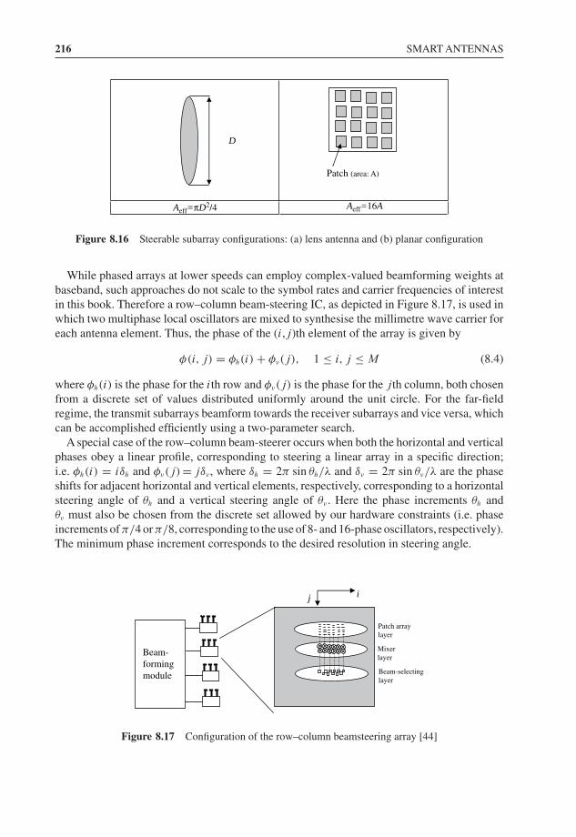
216 SMART ANTENNAS
Aeff=16AAeff=πD2/4
D
Patch (area: A)
Figure 8.16 Steerable subarray configurations: (a) lens antenna and (b) planar configuration
While phased arrays at lower speeds can employ complex-valued beamforming weights atbaseband, such approaches do not scale to the symbol rates and carrier frequencies of interestin this book. Therefore a row–column beam-steering IC, as depicted in Figure 8.17, is used inwhich two multiphase local oscillators are mixed to synthesise the millimetre wave carrier foreach antenna element. Thus, the phase of the (i,j )th element of the array is given by
φ(i, j) = φh(i) + φν(j), 1 ≤ i, j ≤ M (8.4)
where φh(i) is the phase for the ith row and φν(j) is the phase for the j th column, both chosenfrom a discrete set of values distributed uniformly around the unit circle. For the far-fieldregime, the transmit subarrays beamform towards the receiver subarrays and vice versa, whichcan be accomplished efficiently using a two-parameter search.
A special case of the row–column beam-steerer occurs when both the horizontal and verticalphases obey a linear profile, corresponding to steering a linear array in a specific direction;i.e. φh(i) = iδh and φν(j) = jδν , where δh = 2π sin θh/λ and δν = 2π sin θν/λ are the phaseshifts for adjacent horizontal and vertical elements, respectively, corresponding to a horizontalsteering angle of θh and a vertical steering angle of θν . Here the phase increments θh andθν must also be chosen from the discrete set allowed by our hardware constraints (i.e. phaseincrements of π/4 or π/8, corresponding to the use of 8- and 16-phase oscillators, respectively).The minimum phase increment corresponds to the desired resolution in steering angle.
Beam-formingmodule
Patch arraylayer
Mixerlayer
Beam-selectinglayer
ij
Figure 8.17 Configuration of the row–column beamsteering array [44]
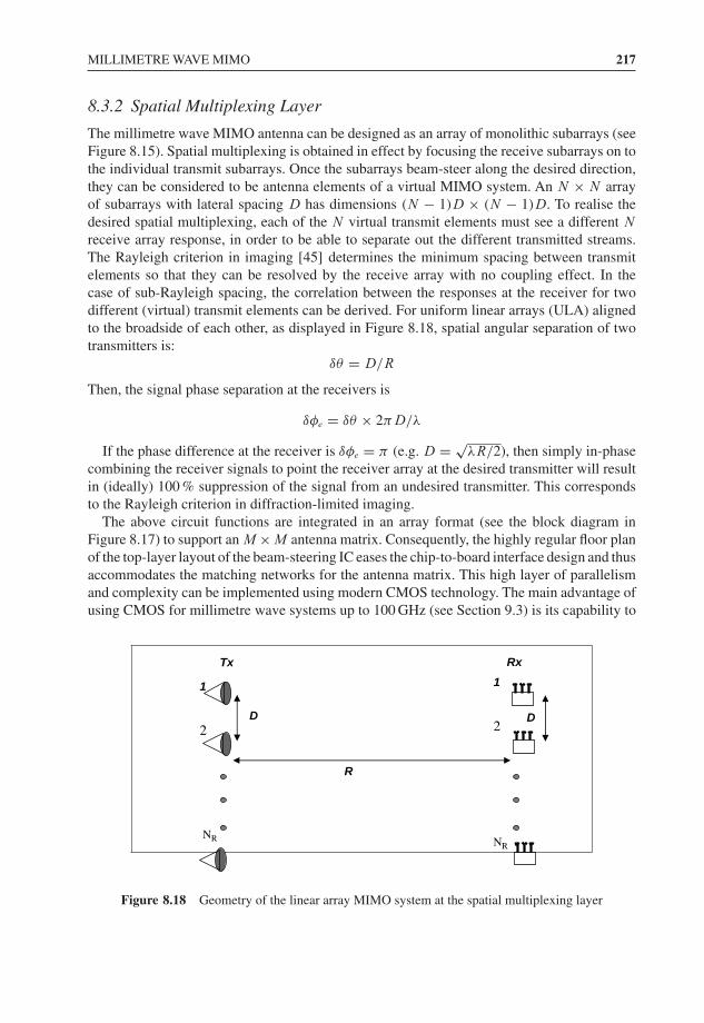
MILLIMETRE WAVE MIMO 217
8.3.2 Spatial Multiplexing Layer
The millimetre wave MIMO antenna can be designed as an array of monolithic subarrays (seeFigure 8.15). Spatial multiplexing is obtained in effect by focusing the receive subarrays on tothe individual transmit subarrays. Once the subarrays beam-steer along the desired direction,they can be considered to be antenna elements of a virtual MIMO system. An N × N arrayof subarrays with lateral spacing D has dimensions (N − 1)D × (N − 1)D. To realise thedesired spatial multiplexing, each of the N virtual transmit elements must see a different N
receive array response, in order to be able to separate out the different transmitted streams.The Rayleigh criterion in imaging [45] determines the minimum spacing between transmitelements so that they can be resolved by the receive array with no coupling effect. In thecase of sub-Rayleigh spacing, the correlation between the responses at the receiver for twodifferent (virtual) transmit elements can be derived. For uniform linear arrays (ULA) alignedto the broadside of each other, as displayed in Figure 8.18, spatial angular separation of twotransmitters is:
δθ = D/R
Then, the signal phase separation at the receivers is
δφe = δθ × 2πD/λ
If the phase difference at the receiver is δφe = π (e.g. D = √λR/2), then simply in-phase
combining the receiver signals to point the receiver array at the desired transmitter will resultin (ideally) 100 % suppression of the signal from an undesired transmitter. This correspondsto the Rayleigh criterion in diffraction-limited imaging.
The above circuit functions are integrated in an array format (see the block diagram inFigure 8.17) to support an M × M antenna matrix. Consequently, the highly regular floor planof the top-layer layout of the beam-steering IC eases the chip-to-board interface design and thusaccommodates the matching networks for the antenna matrix. This high layer of parallelismand complexity can be implemented using modern CMOS technology. The main advantage ofusing CMOS for millimetre wave systems up to 100 GHz (see Section 9.3) is its capability to
Rx
1
2
NR
R
D
Tx
1
2
NR
D
Figure 8.18 Geometry of the linear array MIMO system at the spatial multiplexing layer
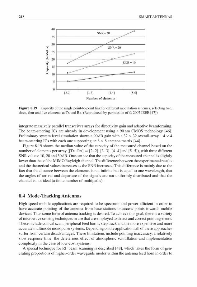
218 SMART ANTENNAS
[2.2]0
5
10
15
20
25
30
35
40
[3.3] [4.4] [5.5]
Number of elements
Cap
acit
y (b
its/
s/H
z)
SNR = 10
SNR = 20
SNR = 30
Figure 8.19 Capacity of the single point-to-point link for different modulation schemes, selecting two,three, four and five elements at Tx and Rx. (Reproduced by permission of © 2007 IEEE [47])
integrate massively parallel transceiver arrays for directivity gain and adaptive beamforming.The beam-steering ICs are already in development using a 90 nm CMOS technology [46].Preliminary system level simulation shows a 90 dB gain with a 32 × 32 overall array −4 × 4beam-steering ICs with each one supporting an 8 × 8 antenna matrix [44].
Figure 8.19 shows the median value of the capacity of the measured channel based on thenumber of elements per array ([Tx ·Rx] = [2 ·2], [3 ·3], [4 ·4] and [5 ·5]), with three differentSNR values: 10, 20 and 30 dB. One can see that the capacity of the measured channel is slightlylower than that of the MIMO Rayleigh channel. The difference between the experimental resultsand the theoretical values increases as the SNR increases. This difference is mainly due to thefact that the distance between the elements is not infinite but is equal to one wavelength, thatthe angles of arrival and departure of the signals are not uniformly distributed and that thechannel is not ideal (a finite number of multipaths).
8.4 Mode-Tracking Antennas
High-speed mobile applications are required to be spectrum and power efficient in order tohave accurate pointing of the antenna from base stations or access points towards mobiledevices. Thus some form of antenna tracking is desired. To achieve this goal, there is a varietyof microwave sensing techniques in use that are employed to detect and correct pointing errors.These include conical scan, peripheral feed horns, step track and the more expensive and moreaccurate multimode monopulse systems. Depending on the application, all of these approachessuffer from certain disadvantages. These limitations include pointing inaccuracy, a relativelyslow response time, the deleterious effect of atmospheric scintillation and implementationcomplexity in the case of low-cost systems.
A special technique for RF beam scanning is described [48], which takes the form of gen-erating proportions of higher-order waveguide modes within the antenna feed horn in order to
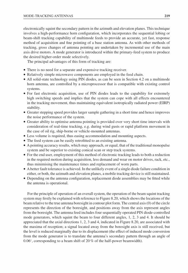
MODE-TRACKING ANTENNAS 219
electronically squint the secondary pattern in the azimuth and elevation planes. This techniqueinvolves a high-performance horn configuration, which incorporates the sequential lobing orbeam-shift tracking capability of multimode feeds to provide an accurate, yet fast, responsemethod of acquisition and fine pointing of a base station antenna. As with other methods oftracking, gross changes of antenna pointing are undertaken by incremental use of the mainaxis drive motors. A mode generator is introduced within the primary-feed system to producethe desired higher-order mode selectively.
The principal advantages of this form of tracking are:
• There is no need for a separate and expensive tracking receiver.• Relatively simple microwave components are employed in the feed chain.• All solid-state technology using PIN diodes, as can be seen in Section 4.2 on a multimode
horn antenna, are controlled by a microprocessor that is compatible with existing controlsystems.
• For fast electronic acquisition, use of PIN diodes leads to the capability for extremelyhigh switching speeds and implies that the system can cope with all effects encounteredin the tracking movement, thus maintaining equivalent isotropically radiated power (EIRP)stability.
• Greater stepping speed provides larger sample gathering in a short time and hence improvesthe noise performance of the system.
• Greater ability to optimise antenna pointing is provided over very short time intervals withconsideration of real-time tracking, e.g. during wind gusts or rapid platform movement inthe case of oil rig, ship-borne or vehicle-mounted antennas.
• Less volume is required, thus easing accommodation and mounting aspects.• The feed system can be easily retrofitted to an existing antenna.• A pointing accuracy results, which may approach, or equal, that of the traditional monopulse
system and be superior to existing conical scan or step track systems.• For the end user, employment of this method of electronic tracking leads to both a reduction
in the required motion during acquisition, less demand and wear on motor drives, rack, etc.,thus minimising the maintenance times and replacement of worn parts.
• Abetter fault tolerance is achieved. In the unlikely event of a single diode failure condition ineither, or both, the azimuth and elevation planes, a mobile tracking device is still maintained.
• Depending on the antenna configuration, replacement diode assemblies may be fitted whilethe antenna is operational.
For the principle of operation of an overall system, the operation of the beam squint trackingsystem may firstly be explained with reference to Figure 8.20, which shows the locations of thebeam relative to the true antenna boresight in contour plot form. The central axis (0) of the circlerepresents the direction of the boresight, and positions away from the axis represent anglesfrom the boresight. The antenna feed includes four sequentially operated PIN diode-controlledmode generators, which squint the beam to four different angles, 1, 2, 3 and 4. It should beappreciated that the axial directions 1, 2, 3 and 4, indicated in Figure 8.20, are associated withthe maxima of reception; a signal located away from the boresight axis is still received, butthe level is reduced marginally due to its displacement (the effect of induced mode conversionfrom the mode generator is to translate the antenna’s secondary pattern through an angle of0.06◦, corresponding to a beam shift of 20 % of the half-power beamwidth).
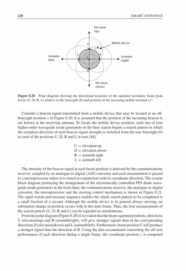
220 SMART ANTENNAS
Azimuth(right)
Azimuth(left)
Elevation(up)
Elevation(down)
U
D
L R
x
Mobile device
0
Figure 8.20 Polar diagram showing the directional locations of the squinted secondary beam peaklevels (U, D, R, L) relative to the boresight (0) and position of the incoming mobile terminal (x)
Consider a beacon signal transmitted from a mobile device that may be located at an off-boresight position x in Figure 8.20. It is assumed that the position of the incoming beacon isnot known at the receiving antenna. To locate the mobile device position, each one of fourhigher-order waveguide mode generators in the base station begins a search pattern in whichthe reception direction of each beacon signal strength is switched from the true boresight (0)to each of the positions U, D, R and L in turn [48]:
U = elevation upD = elevation downR = azimuth rightL = azimuth left
The intensity of the beacon signal at each beam position is detected by the communicationsreceiver, sampled by an analogue-to-digital (A/D) converter and each measurement is passedto a microprocessor where it is stored in conjunction with its coordinate direction. The systemblock diagram portraying the arrangement of the electronically controlled PIN diode wave-guide mode generators in the feed chain, the communications receiver, the analogue-to-digitalconverter, the microprocessor and the steering control mechanism is shown in Figure 8.21.The rapid switch-and-measure sequence enables the whole search pattern to be completed ina small fraction of a second. Although the mobile device is in general always moving, nosubstantial change in position occurs with in this time frame. Thus, the four measurements ofthe search pattern (U, D, R and L) can be regarded as simultaneous.
From the polar diagram (Figure 8.20) it is evident that the beam squinted positions, directionsU (elevation/up) and R (azimuth/right), will give stronger signals than in the correspondingdirections D (elevation/down) and L (azimuth/left). Furthermore, beam position U will producea stronger signal than the direction of R. Using the data accumulated concerning the off-axisperformance of each direction during a single frame, the coordinate position x is computed
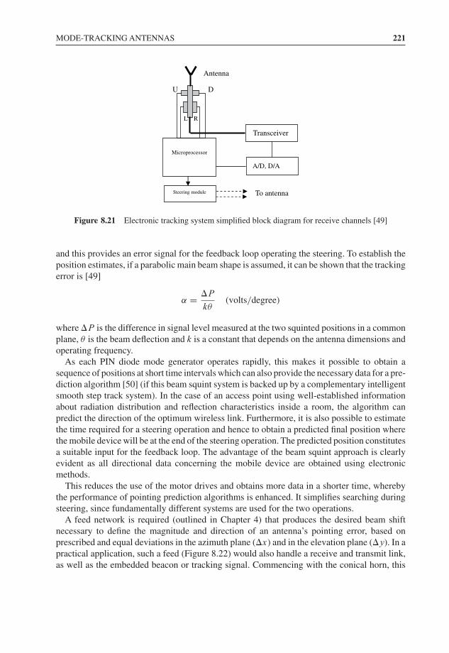
MODE-TRACKING ANTENNAS 221
Microprocessor
Antenna
U D
L R
Transceiver
A/D, D/A
Steering module To antenna
Figure 8.21 Electronic tracking system simplified block diagram for receive channels [49]
and this provides an error signal for the feedback loop operating the steering. To establish theposition estimates, if a parabolic main beam shape is assumed, it can be shown that the trackingerror is [49]
α = �P
kθ(volts/degree)
where �P is the difference in signal level measured at the two squinted positions in a commonplane, θ is the beam deflection and k is a constant that depends on the antenna dimensions andoperating frequency.
As each PIN diode mode generator operates rapidly, this makes it possible to obtain asequence of positions at short time intervals which can also provide the necessary data for a pre-diction algorithm [50] (if this beam squint system is backed up by a complementary intelligentsmooth step track system). In the case of an access point using well-established informationabout radiation distribution and reflection characteristics inside a room, the algorithm canpredict the direction of the optimum wireless link. Furthermore, it is also possible to estimatethe time required for a steering operation and hence to obtain a predicted final position wherethe mobile device will be at the end of the steering operation. The predicted position constitutesa suitable input for the feedback loop. The advantage of the beam squint approach is clearlyevident as all directional data concerning the mobile device are obtained using electronicmethods.
This reduces the use of the motor drives and obtains more data in a shorter time, wherebythe performance of pointing prediction algorithms is enhanced. It simplifies searching duringsteering, since fundamentally different systems are used for the two operations.
A feed network is required (outlined in Chapter 4) that produces the desired beam shiftnecessary to define the magnitude and direction of an antenna’s pointing error, based onprescribed and equal deviations in the azimuth plane (�x) and in the elevation plane (�y). In apractical application, such a feed (Figure 8.22) would also handle a receive and transmit link,as well as the embedded beacon or tracking signal. Commencing with the conical horn, this
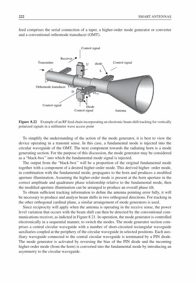
222 SMART ANTENNAS
feed comprises the serial connection of a taper, a higher-order mode generator or converterand a conventional orthomode transducer (OMT).
TE21
TM01
R
L
D
UTransmitterReceiver
Control signal
Control signal
Control signal
Control signal
Orthomode transducer
AntennaDiode
diode
Figure 8.22 Example of an RF feed chain incorporating an electronic beam shift tracking for verticallypolarized signals in a millimetre wave access point
To simplify the understanding of the action of the mode generator, it is best to view thedevice operating in a transmit sense. In this case, a fundamental mode is injected into thecircular waveguide of the OMT. The next component towards the radiating horn is a modegenerating section. For the purpose of this discussion, the mode generator may be consideredas a “black-box’’ into which the fundamental mode signal is injected.
The output from the “black-box’’ will be a proportion of the original fundamental modetogether with a component of a desired higher-order mode. This derived higher- order mode,in combination with the fundamental mode, propagates to the horn and produces a modifiedaperture illumination. Assuming the higher-order mode is present at the horn aperture in thecorrect amplitude and quadrature phase relationship relative to the fundamental mode, thenthe modified aperture illumination can be arranged to produce an overall phase tilt.
To obtain sufficient tracking information to define the antenna pointing error fully, it willbe necessary to produce and analyse beam shifts in two orthogonal directions. For tracking inthe other orthogonal cardinal plane, a similar arrangement of mode generators is used.
Since reciprocity will apply when the antenna is operating in the receive sense, the powerlevel variation that occurs with the beam shift can then be detected by the conventional com-munications receiver, as indicted in Figure 8.21. In operation, the mode generator is controlledelectronically in a sequential manner, to switch the modes. The mode generator section com-prises a central circular waveguide with a number of short-circuited rectangular waveguideauxiliaries coupled at the periphery of the circular waveguide in selected positions. Each aux-iliary waveguide connected to the central circular waveguide is terminated by a PIN diode.The mode generator is activated by reversing the bias of the PIN diode and the incominghigher-order mode (from the horn) is converted into the fundamental mode by introducing anasymmetry to the circular waveguide.
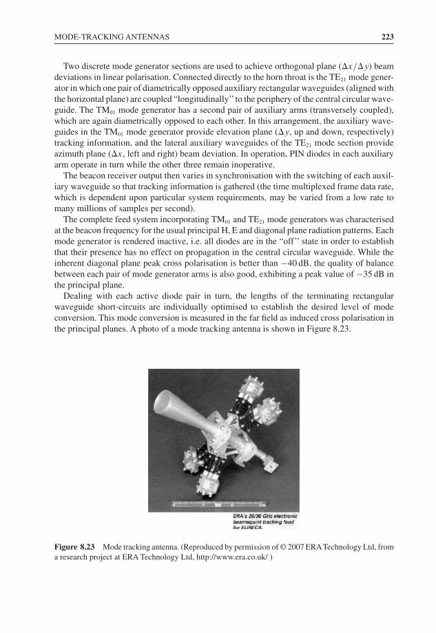
MODE-TRACKING ANTENNAS 223
Two discrete mode generator sections are used to achieve orthogonal plane (�x/�y) beamdeviations in linear polarisation. Connected directly to the horn throat is the TE21 mode gener-ator in which one pair of diametrically opposed auxiliary rectangular waveguides (aligned withthe horizontal plane) are coupled “longitudinally’’ to the periphery of the central circular wave-guide. The TM01 mode generator has a second pair of auxiliary arms (transversely coupled),which are again diametrically opposed to each other. In this arrangement, the auxiliary wave-guides in the TM01 mode generator provide elevation plane (�y, up and down, respectively)tracking information, and the lateral auxiliary waveguides of the TE21 mode section provideazimuth plane (�x, left and right) beam deviation. In operation, PIN diodes in each auxiliaryarm operate in turn while the other three remain inoperative.
The beacon receiver output then varies in synchronisation with the switching of each auxil-iary waveguide so that tracking information is gathered (the time multiplexed frame data rate,which is dependent upon particular system requirements, may be varied from a low rate tomany millions of samples per second).
The complete feed system incorporating TM01 and TE21 mode generators was characterisedat the beacon frequency for the usual principal H, E and diagonal plane radiation patterns. Eachmode generator is rendered inactive, i.e. all diodes are in the “off’’ state in order to establishthat their presence has no effect on propagation in the central circular waveguide. While theinherent diagonal plane peak cross polarisation is better than −40 dB, the quality of balancebetween each pair of mode generator arms is also good, exhibiting a peak value of −35 dB inthe principal plane.
Dealing with each active diode pair in turn, the lengths of the terminating rectangularwaveguide short-circuits are individually optimised to establish the desired level of modeconversion. This mode conversion is measured in the far field as induced cross polarisation inthe principal planes. A photo of a mode tracking antenna is shown in Figure 8.23.
Figure 8.23 Mode tracking antenna. (Reproduced by permission of © 2007 ERATechnology Ltd, froma research project at ERA Technology Ltd, http://www.era.co.uk/ )
224 SMART ANTENNAS
Table 8.4 Summary of various classes of smart antennas
Spatialtechnique
Aspects Pros Cons
Beamswitching
Switching among set ofpredefined fixedmultiple beams
Easy to implement. Nophase shifter is needed.Stable performance when allusers have low/ similar datarates
Underperforms in systemswith multirate serviceswhere both low data ratespeech service and highdata rate applications aresimultaneously supportedsince beams cannot trackusers
Beamsteering
Main beam is directedtowards the desired user
Weight is the same as thesteering vector
Provides array gainand steering gain forspatially white interferenceenvironments
Requires direction ofarrival estimation of thedesired user
Suboptimal performance interms of SNR or SIR
MIMO The most adaptivescheme
SNR and SINR areoptimised based onsome given criterion
Increase diversity andcapacity
Optimal weight vector andoptimal performance
Computationally intensive.Multiple transceivers areneeded
SINR: signal to interference plus noise ratio.
In summary, this chapter concludes by comparing the various classes, both in the light ofcurrently obtained results and with respect to the underlying trends (Table 8.4).
References[1] B. Neekzad, K. Sazrafian-Pour and J. D. Baras, ‘Clustering Characteristics of Millimeter Wave Indoor Channels’,
IEEE Wireless Communications and Networking Conference, 2008.[2] M. A. Beach, A. J. Copping, D. J. Edwards and K. W. Yates, ‘An Adaptive Antenna for Multiple Signal
Sources’, 5th International Conference on ‘Antennas and Propagation’, York, England, 30 March–2 April 1987,pp. 347–350.
[3] A. M. Street, A. P. Jenkins, J. Thornton and D. J. Edwards, ‘Low Cost Adaptive Antenna Systems for IndoorMobile Wireless Communications’, AP2000 Millennium Conference on ‘Antennas and Propagation’, Davos,Switzerland, 9–14 April 2000, ESA.
[4] http://dept106.eng.ox.ac.uk/wb/pages/research/microwave/radar-and-antennas/adaptive-antennas.php[5] J. Butler and R. Howe, ‘Beamforming Matrix Simplifies Design of Electronically ScannedAntennas’, Electronics
Design, 9, 1961, 170–173.[6] J. P. Shelton and K. S. Kelleher, ‘Multiple Beams for Linear Arrays’, IRE Transactions on Antennas and
Propagation, March 1961, 154–161.[7] P. J. Muenzer, ‘Properties of Linear Phased Arrays Using Butler Matrices’, Standard Elektrik, A. G. Lorenz,
Stuttgart, NTZ, 9, 1972, 419–422.[8] T. MacNamara, ‘Simplified Design Procedure for Butler Matrices Incorporating 90’’ or 180’’ hybrids’, IEE
Proceedings H, Microwaves, Antennas and Propagation, 134(I), 1987, 50–54.

REFERENCES 225
[9] J. Shelton and J. Hsiao, ‘Reflective Butler Matrix’, IEEE Transactions on Antennas and Propagation, AP-27(5),1979, 651–659.
[10] J. R. F. Guy, ‘Proposal to Use Reflected Signals through a Single Butler Matrix to Produce Multiple Beams froma Circular Array Antenna’, Electronics Letters, 28(5), 1985, 209–211.
[11] S. Ohshima, Y. Asano, T. Harada, N. Yamada, M. Usui, H. Hayashi, T. Watanabe and H. Iizuka, ‘Phase-Comparison Monopulse Radar with Switched Transmit Beams for Automotive Application’, IEEE MTT-SInternational Microwave Symposium Digest, 4, 1999, 1493–1496.
[12] G. N. Hulderman, ‘Stepped BeamActiveArrayAntenna and Radar System Employing Same, US Patent 5583511,1996.
[13] R. Roy and T. Kailath, ‘ESPRIT – Estimation of Signal Parameters via Rotational Invariance Techniques’, IEEETransactions on Acoustics and Speech Signal Process, 37, 1989, 984–995.
[14] Y. Asano, S. Ohshima, T. Harada, M. Ogawa and K. Nishikawa, ‘Proposal of Millimeter-Wave HolographicRadar with Antenna Switching’, IEEE MTT-S International Microwave Symposium Digest, 2, 2001, 1111–1114.
[15] N. Kikuma, ‘Adaptive Signal Processing with Array Antenna’, Science and Technology Publishing Company,1998.
[16] S. Ohshima, Y. Asano and K. Nishikawa, ‘A Method for Accomplishing Accurate RCS Image’, IEICETransactions on Communications, E79-B, 1996, 1799–1805.
[17] N. Yamada, Y. Asano, S. Ohshima and K. Nishikawa, ‘3-Dimensional High-Resolution Measurement of RadarCross Section for Car in 76 GHz Band’, Proceedings of the 2003 IEICE General Conference, B-1-11, 2003.
[18] Masaru Ogawa, Yoshikazu Asano, Shigeki Ohshima, Tomohisa Harada and Naoyuki Yamada, ‘ElectricallyScanned Millimeter-Wave Radar with Antenna Switching’, Electronics and Communications in Japan, Part 3,89(1), 2006, Translated from Denshi Joho Tsushin, ‘Gakkai Ronbunshi’, Vol. J88-A, No. 2, February 2005,pp. 237–246.
[19] Graham Brooker, Mark Bishop and Steve Seheding, ‘Millimetre Waves for Robotics’, Proceedings of 2001Australian Conference on ‘Tobotics and Automation’, November 2001, pp. 91–97.
[20] K. Yamane, A. Sanada and K. Ohkubo, ‘A Holographic Imaging Method for Automotive Radar’, Transactionsof IEICE, J81-B-II, 1998, 805–813.
[21] C. Barth, K. Caekenberghe and K. Sarabandi, ‘A Novel Low-Cost Millimeter-Wave Beam-Steering System’,IEEE.APS International Symposium, Vol. 4B, 2005, pp. 31–34.
[22] A. Abbaspour-Tamijani, K. Sarabandi and G. M. Rebeiz, ‘A Planar Filter–Lens Array for Milimeter-WaveApplications’, IEEE Transactions on Antennas and Propagation, 1, 2004, 675–678.
[23] A. Abbaspour-Tamijani and K. Sarabandi, ‘An Affordable Millimeter-Wave Beam-Steerable Antenna UsingInterleaved Planar Subarrays’, IEEE Transactions on Antennas and Propagation, 51(9), September 2003,2193–2202.
[24] P.S. Hall and S.J. Vetterlein, ‘Review of Radio Frequency Beamforming Techniques for Scanned and MultipleBeam Antennas’, IEE Proceedings, Part H, 137(5), October 1990, 293–303.
[25] W. D. White, ‘Pattern Limitation in Multiple Beam Antennas’, IRE Transactions on Antennas and Propagation,July 1962, 430–436.
[26] J. Blass, ‘Multi-directionalAntenna – NewApproach Top Stacked Beams’, IRE International Convention Record,Part 1, 1960, 48–50
[27] R. C. Hansen, ‘Microwave Scanning Antennas’, Vol.111, Academic Press, New York, 1966, p. 246.[28] M. Fassett, L. J. Kaplan and J. H. Pozgay, ‘Optimal Synthesis of Ladder Network Array Antenna Feed Systems’,
APS Symposium, Amherst, Massachusetts, 11–15 October 1976, pp. 58–61.[29] N. Inagaki, ‘Synthesis on Beam Forming Networks for Multiple Beam Array Antennas with Maximum Feed
Efficiency’, IEE International Conference on ‘Antennas and Propagation’, ICAP 87, March 1987, pp. 375–378[30] P. J. Wood, ‘An Efficient Matrix Feed for anArray Generating Overlapped Beams’, IEE International Conference
on ‘Antennas and Propagation’, ICAP 87, March 1987, pp. 371–374.[31] S. J. Vetterlein and P. S. Hall, ‘Novel Multiple Beam Microstrip Patch Array with Integrated Beamformer’,
Electronics Letters, 25(17), 1989.[32] P. E. K. Chow and D. E. N. Davis, ‘Wide Bandwidth Butler Matrix Network’, Electronics Letters, 3, 1967,
252–253.[33] R. Levy, ‘A High Power X Band Butler Matrix’, Microwave Journal, April 1984, 135.[34] J. R. Wallington, ‘Analysis, Design and Performance of a Microstrip Butler Matrix’, European Microwave
Conference, Brussels, 4–7 September 1973, Vol. 1, pp. A1431–A.1434.

226 SMART ANTENNAS
[35] G. Skahill and W. D. White, ‘A New Technique for Feeding a Circular Array’, IEEE Transactions on Antennasand Propagation, AP-23, March 1975, 253–256.
[36] B. Sheleg, ‘A Matrix Fed Circular Array for Continuous Scanning’. IEEE APS Symposium, Boston,Massachusetts, 9–11 September 1986, pp. 7–16.
[37] Antoine J. Rouphael, ‘Adaptive Beamforming in a Wireless Communication system’, US Patent 20040204103.[38] K. Ohata, K. Maruhashi, M. Ito, S. Kishimoto K. Ikuina, T. Hashiguchi, K. Ikeda and N. Takahashi, ‘1.25 Gb/s
Wireless Gigabit Ethernet Link at 60 GHz-Band’, IEEE MTT-S International Microwave Symposium Digest, 1,June 2003, 373–376.
[39] Proxim-WirelessTM, ‘Gigalink Series – Alternative to Fiber up to Gigabit Speeds’, DS 0806 GIGALINKUSHR.pdf, 2006.
[40] John G. Proakis, ‘Digital Communications’, McGraw-Hill, New York, 4th edition, 2000.[41] Angel Lozano, Farrokh R. Farrokhi and Reinaldo A. Valenzuela, ‘Lifting the Limits on High-Speed Wireless
Data Access Using Antenna Arrays’, IEEE Communications Magazine, September 2001, 156–162.[42] Gregory D. Durgin, ‘Space–Time Wireless Channels’, Prentice-Hall, New Jersey, 2003.[43] E. Telatar, ‘Capacity of Multi-antenna Gaussian Channels’, Technical Report, AT&T Bell Labs, 1995.[44] Eric Torkildson, Bharath Ananthasubramaniam, Upamanyu Madhow and Mark Rodwell, ‘Millimeter-Wave
MIMO: Wireless Links at Optical Speeds’ (Invited Paper), Proceedings of the 44th Annual Allerton Conferenceon ‘Communication, Control and Computing’, Monticello, Illinois, September 2006.
[45] J. D. Kraus, ‘Radio Astronomy’, 2nd edition, Cygnus-Quasar, 1986, pp. 6–19.[46] C. Carta, M. Seo and M. Rodwell, ‘A Mixed Signal Row/Column Architecture for Very Large Monolithic
mm-Wave Phased Arrays’, IEEE Lester Eastman Conference on ‘High Performance Devices’, August 2006.[47] Sylvain Ranvier, Jarmo Kivinen and Pertti Vainikainen, ‘Millimeter-Wave MIMO Radio Channel Sounder’,
IEEE Transactions on Instrumentation and Measurement, 56(3), June 2007, 1018–1024.[48] D. J. Edwards and B. K. Watson, ‘Electronic Tracking Systems for Microwave Antennas’, British Patent
Application 8414963, 12 June 1984.[49] R. Dang, B. Watson, I. Davis and D. J. Edwards, ‘Electronic Tracking System for Satellite Ground Stations’,
European Microwave Conference, 1985, pp. 681–687.[50] P. M. Terrell and D. J. Edwards, ‘The Smoothed Step-Track Antenna Controller’, International Journal of
Satellite Communications, 1(2), 1983, 133–139.
9Advanced Antenna Materials
At millimetre wave frequencies, materials and integration techniques in RF systems are subjectto more demanding performance constraints. One example in printed technologies is substratewater absorption, which above 10 GHz can cause unacceptable losses in elements such asantennas, filters and transmission lines, particularly over extended periods of time and underconditions of varying humidity. Many materials, which are used for 2.4 and 5.8 GHz wirelesslocal area networks, may also have high dielectric loss for millimetre wave applications. Inaddition, the market demands improved performance at low cost. Thus, new material tech-nologies must be identified that can simultaneously fulfil these requirements of performance,frequency and environmental invariance, and low cost.
Millimetre wave systems tend to be designed around two major philosophies: system-on-chip (SoC) and system-on-package (SoP). System-on-chip is a fully integrated design approachwith RF passive components and digital and/or optical functions on-wafer [1]. System-on-package incorporates analogue components into a multilayer dielectric material and integrateschips within or on the same dielectric packaging material [2]. For the system-on-chip approach,especially for millimetre waves, gallium arsenide (GaAs) is normally used owing to the highcut-off frequency performance it offers digital transistors, and for the lower substrate loss itprovides for analogue components. However, GaAs is much more expensive than silicon, andusing large areas of the substrate for analogue components is not deemed to be cost effective.Silicon germanium (SiGe) on either CMOS/BiCMOS-grade silicon (Si) or high-resistivity Siis a lower cost option than GaAs for some applications, but it is still a relatively lossy substratefor passive RF components. System-on-package (SoP) modules solve the major shortfalls ofsystem-on-chip (SoC), by providing a low-loss substrate material for the RF passives and aunique space-saving capability for chip integration in or on the substrate.
The industry standard for circuit boards, i.e. FR4, becomes unacceptable due to prohibitivelylarge losses and is not suitable for SoP in the high gigahertz range. Low temperature co-firedceramic (LTCC) has attractive electrical characteristics, can support dense multilayer circuitintegration and has very good package hermeticity, but the cost is also relatively high [3].Notwithstanding the cost issues, it is a major candidate in millimetre wave system integration,but owing to its limitation in terms of design rules (i.e. minimum line width and spacing)
Millimetre Wave Antennas for Gigabit Wireless Communications Kao-Cheng Huang and David J. Edwardsc© 2008 John Wiley & Sons, Ltd
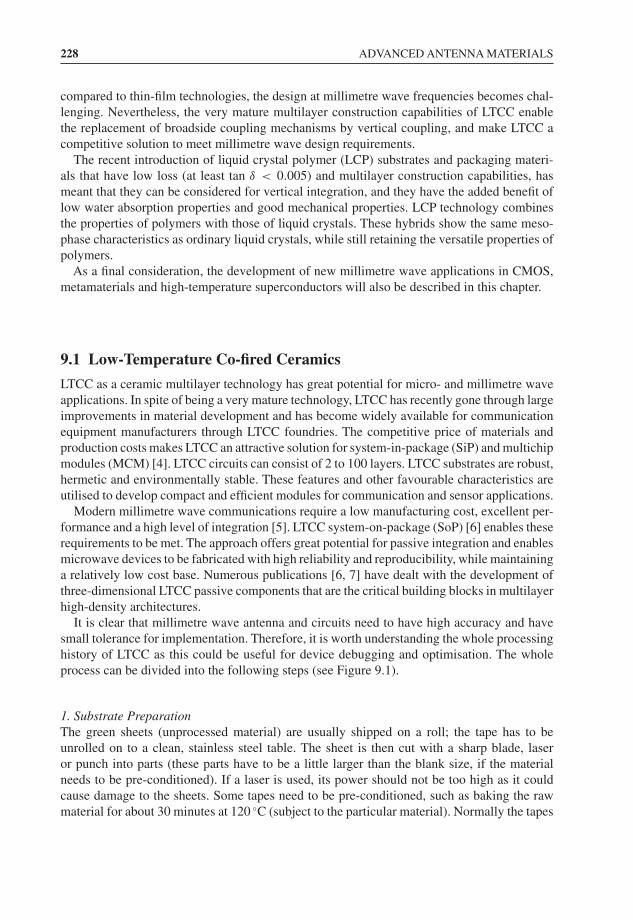
228 ADVANCED ANTENNA MATERIALS
compared to thin-film technologies, the design at millimetre wave frequencies becomes chal-lenging. Nevertheless, the very mature multilayer construction capabilities of LTCC enablethe replacement of broadside coupling mechanisms by vertical coupling, and make LTCC acompetitive solution to meet millimetre wave design requirements.
The recent introduction of liquid crystal polymer (LCP) substrates and packaging materi-als that have low loss (at least tan δ < 0.005) and multilayer construction capabilities, hasmeant that they can be considered for vertical integration, and they have the added benefit oflow water absorption properties and good mechanical properties. LCP technology combinesthe properties of polymers with those of liquid crystals. These hybrids show the same meso-phase characteristics as ordinary liquid crystals, while still retaining the versatile properties ofpolymers.
As a final consideration, the development of new millimetre wave applications in CMOS,metamaterials and high-temperature superconductors will also be described in this chapter.
9.1 Low-Temperature Co-fired Ceramics
LTCC as a ceramic multilayer technology has great potential for micro- and millimetre waveapplications. In spite of being a very mature technology, LTCC has recently gone through largeimprovements in material development and has become widely available for communicationequipment manufacturers through LTCC foundries. The competitive price of materials andproduction costs makes LTCC an attractive solution for system-in-package (SiP) and multichipmodules (MCM) [4]. LTCC circuits can consist of 2 to 100 layers. LTCC substrates are robust,hermetic and environmentally stable. These features and other favourable characteristics areutilised to develop compact and efficient modules for communication and sensor applications.
Modern millimetre wave communications require a low manufacturing cost, excellent per-formance and a high level of integration [5]. LTCC system-on-package (SoP) [6] enables theserequirements to be met. The approach offers great potential for passive integration and enablesmicrowave devices to be fabricated with high reliability and reproducibility, while maintaininga relatively low cost base. Numerous publications [6, 7] have dealt with the development ofthree-dimensional LTCC passive components that are the critical building blocks in multilayerhigh-density architectures.
It is clear that millimetre wave antenna and circuits need to have high accuracy and havesmall tolerance for implementation. Therefore, it is worth understanding the whole processinghistory of LTCC as this could be useful for device debugging and optimisation. The wholeprocess can be divided into the following steps (see Figure 9.1).
1. Substrate PreparationThe green sheets (unprocessed material) are usually shipped on a roll; the tape has to beunrolled on to a clean, stainless steel table. The sheet is then cut with a sharp blade, laseror punch into parts (these parts have to be a little larger than the blank size, if the materialneeds to be pre-conditioned). If a laser is used, its power should not be too high as it couldcause damage to the sheets. Some tapes need to be pre-conditioned, such as baking the rawmaterial for about 30 minutes at 120 ◦C (subject to the particular material). Normally the tapes
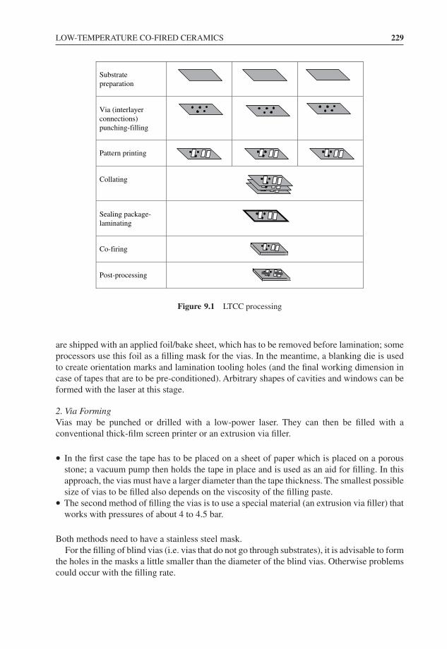
LOW-TEMPERATURE CO-FIRED CERAMICS 229
Substratepreparation
Via (interlayerconnections)punching-filling
Pattern printing
Collating
Sealing package-laminating
Co-firing
Post-processing
Figure 9.1 LTCC processing
are shipped with an applied foil/bake sheet, which has to be removed before lamination; someprocessors use this foil as a filling mask for the vias. In the meantime, a blanking die is usedto create orientation marks and lamination tooling holes (and the final working dimension incase of tapes that are to be pre-conditioned). Arbitrary shapes of cavities and windows can beformed with the laser at this stage.
2. Via FormingVias may be punched or drilled with a low-power laser. They can then be filled with aconventional thick-film screen printer or an extrusion via filler.
• In the first case the tape has to be placed on a sheet of paper which is placed on a porousstone; a vacuum pump then holds the tape in place and is used as an aid for filling. In thisapproach, the vias must have a larger diameter than the tape thickness. The smallest possiblesize of vias to be filled also depends on the viscosity of the filling paste.
• The second method of filling the vias is to use a special material (an extrusion via filler) thatworks with pressures of about 4 to 4.5 bar.
Both methods need to have a stainless steel mask.For the filling of blind vias (i.e. vias that do not go through substrates), it is advisable to form
the holes in the masks a little smaller than the diameter of the blind vias. Otherwise problemscould occur with the filling rate.

230 ADVANCED ANTENNA MATERIALS
3. PrintingCo-fireable conductors, etc., are printed on the green sheet using a conventional thick filmscreen printer. As with the via printing process, a porous stone is used to hold the tape inplace. Printing of the conductor can have high resolution because of the flatness and solventabsorption properties of the tape. After printing, the vias and conductors have to be dried inan oven at 80 to 120 ◦C for 5 to 30 minutes (depending on the material); some pastes needto level (flow) at room temperature for a few minutes before drying. In this process, resistorsmay vary their value when terminated with different conductors.
4. CollatingEach layer constructed in this way is placed in turn over tooling pins. Some foundries use heatto fix the sheets one on top of the other.
5. LaminationThere are two possibilities in laminating the tapes [8].
The first approach is named uniaxial lamination; the tapes are pressed between heatedplatens at 70 ◦C, 200 bar for 10 minutes (typical values). This method causes higher shrinkingtolerances than the second method, of isostatic lamination (see below). The main challenge inthis process is the flowing of the tape, which results in high shrinkage (especially at the edge ofthe wafer) during the firing, and varying thicknesses of each layer (which causes hard problemson the high-frequency sector). Thus uniaxial lamination can possibly cause dimension changeswith cavities/windows.
The second approach is to use an isostatic press. In this approach the stacked tapes arevacuum packaged in a foil and pressed in hot water (similar temperatures and times are usedas in the uniaxial press). The pressure is about 350 bar.
It should be noted that deep cavities and windows need to have an inlay during the laminationprocess.
6. Co-firingLaminates are fired in one step on a smooth, flat setter tile. The firing should follow a specificfiring profile (which means that the temperature must be controlled as a function of time andvaried according to the details of the process). This means that a programmable box kiln mustbe used.
A typical profile shows a (slow) rising temperature (about 2–5 ◦C per minute) up to about450 ◦C with a dwell time of about one to two hours, during which the organic burnout (binder)takes place; then the temperature has to be raised to 850–875 ◦C with a dwell time of about 10to 15 minutes. The whole firing cycle lasts between three and eight hours (depending on thematerial; large/thick parts require a modification of the firing profile).
Note that resistor pastes need to have especially well defined firing conditions (temperatures),otherwise the final resistance value varies enormously.
7. Post-processingSome materials need to be post-fired; this means the paste is to be applied after firing the tapeand then a second firing is undergone. Post-firing thick-film resistors are normally used in 90 ◦
hybrid couplers and smart antennas. Resistor pastes need to have defined firing conditions(temperatures) to achieve the correct resistance. Solder conductors are also processed at thepost-firing phase.
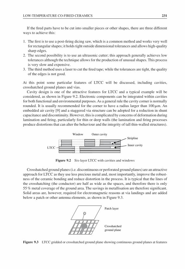
LOW-TEMPERATURE CO-FIRED CERAMICS 231
If the fired parts have to be cut into smaller pieces or other shapes, there are three differentways to achieve this:
1. The first is to use a post-firing dicing saw, which is a common method and works very wellfor rectangular shapes; it holds tight outside dimensional tolerances and allows high-qualitysharp edges.
2. The second possibility is to use an ultrasonic cutter; this approach generally achieves lowtolerances although the technique allows for the production of unusual shapes. This processis very slow and expensive.
3. The third method uses a laser to cut the fired tape; while the tolerances are tight, the qualityof the edges is not good.
At this point some particular features of LTCC will be discussed, including cavities,crosshatched ground planes and vias.
Cavity design is one of the attractive features for LTCC and a typical example will beconsidered, as shown in Figure 9.2. Electronic components can be integrated within cavitiesfor both functional and environmental purposes. As a general rule the cavity corner is normallyrounded. It is usually recommended for the corner to have a radius larger than 100 �m. Anembedded air cavity [9] and a staggered via structure can be adopted for a reduction in shuntcapacitance and discontinuity. However, this is complicated by concerns of deformation duringlamination and firing, particularly for thin or deep walls (the lamination and firing processesproduce distortions that can alter the behaviour and the integrity of tall thin-walled structures).
Stripline
Inner cavity
Window
LTCC
Outer cavity
Figure 9.2 Six-layer LTCC with cavities and windows
Crosshatched ground planes (i.e. discontinuous or perforated ground planes) are an attractiveapproach for LTCC as they use less precious metal and, most importantly, improve the robust-ness of the ceramic bonding and reduce distortion in the process. It is typical that the lines ofthe crosshatching (the conductor) are half as wide as the spaces, and therefore there is only55 % metal coverage of the ground area. The savings in metallisation are therefore significant.Solid areas are, however, required for electromagnetic reasons at via landings and are addedbelow a patch or other antenna elements, as shown in Figure 9.3.
Patch layer
Crosshatchedground plane
Figure 9.3 LTCC gridded or crosshatched ground plane showing continuous ground planes at features
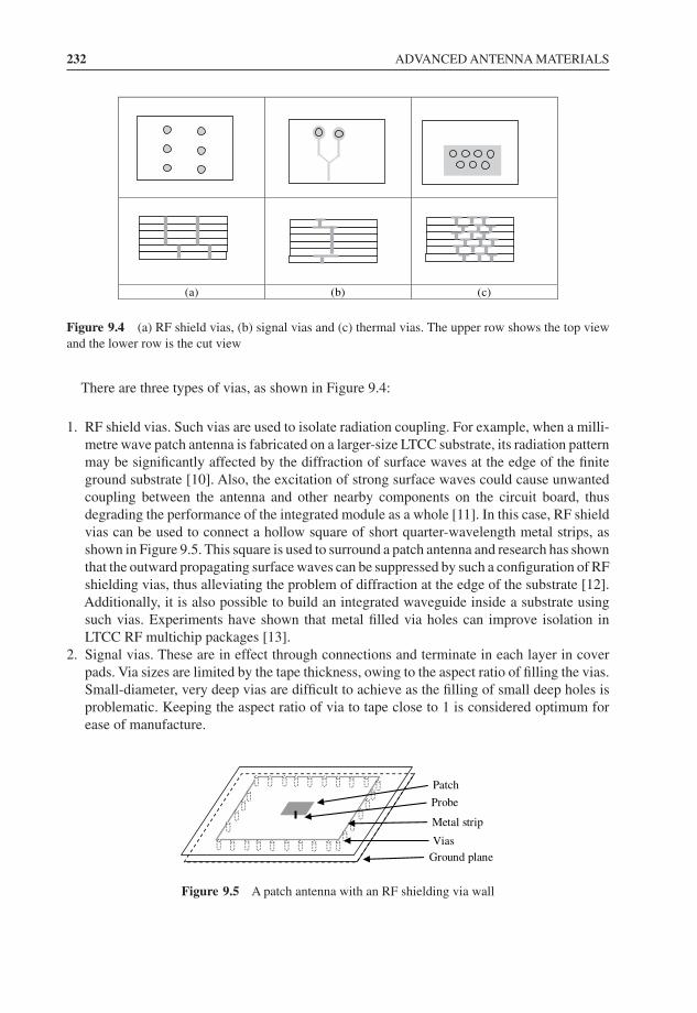
232 ADVANCED ANTENNA MATERIALS
(a) (b) (c)
Figure 9.4 (a) RF shield vias, (b) signal vias and (c) thermal vias. The upper row shows the top viewand the lower row is the cut view
There are three types of vias, as shown in Figure 9.4:
1. RF shield vias. Such vias are used to isolate radiation coupling. For example, when a milli-metre wave patch antenna is fabricated on a larger-size LTCC substrate, its radiation patternmay be significantly affected by the diffraction of surface waves at the edge of the finiteground substrate [10]. Also, the excitation of strong surface waves could cause unwantedcoupling between the antenna and other nearby components on the circuit board, thusdegrading the performance of the integrated module as a whole [11]. In this case, RF shieldvias can be used to connect a hollow square of short quarter-wavelength metal strips, asshown in Figure 9.5. This square is used to surround a patch antenna and research has shownthat the outward propagating surface waves can be suppressed by such a configuration of RFshielding vias, thus alleviating the problem of diffraction at the edge of the substrate [12].Additionally, it is also possible to build an integrated waveguide inside a substrate usingsuch vias. Experiments have shown that metal filled via holes can improve isolation inLTCC RF multichip packages [13].
2. Signal vias. These are in effect through connections and terminate in each layer in coverpads. Via sizes are limited by the tape thickness, owing to the aspect ratio of filling the vias.Small-diameter, very deep vias are difficult to achieve as the filling of small deep holes isproblematic. Keeping the aspect ratio of via to tape close to 1 is considered optimum forease of manufacture.
Patch
Probe
Metal strip
ViasGround plane
Figure 9.5 A patch antenna with an RF shielding via wall
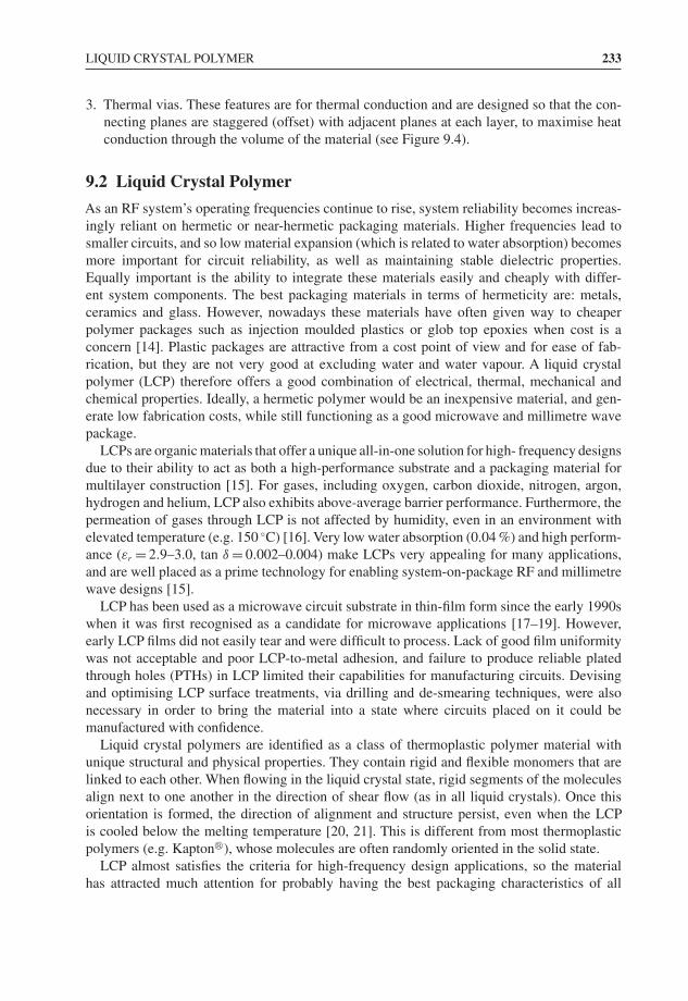
LIQUID CRYSTAL POLYMER 233
3. Thermal vias. These features are for thermal conduction and are designed so that the con-necting planes are staggered (offset) with adjacent planes at each layer, to maximise heatconduction through the volume of the material (see Figure 9.4).
9.2 Liquid Crystal Polymer
As an RF system’s operating frequencies continue to rise, system reliability becomes increas-ingly reliant on hermetic or near-hermetic packaging materials. Higher frequencies lead tosmaller circuits, and so low material expansion (which is related to water absorption) becomesmore important for circuit reliability, as well as maintaining stable dielectric properties.Equally important is the ability to integrate these materials easily and cheaply with differ-ent system components. The best packaging materials in terms of hermeticity are: metals,ceramics and glass. However, nowadays these materials have often given way to cheaperpolymer packages such as injection moulded plastics or glob top epoxies when cost is aconcern [14]. Plastic packages are attractive from a cost point of view and for ease of fab-rication, but they are not very good at excluding water and water vapour. A liquid crystalpolymer (LCP) therefore offers a good combination of electrical, thermal, mechanical andchemical properties. Ideally, a hermetic polymer would be an inexpensive material, and gen-erate low fabrication costs, while still functioning as a good microwave and millimetre wavepackage.
LCPs are organic materials that offer a unique all-in-one solution for high- frequency designsdue to their ability to act as both a high-performance substrate and a packaging material formultilayer construction [15]. For gases, including oxygen, carbon dioxide, nitrogen, argon,hydrogen and helium, LCP also exhibits above-average barrier performance. Furthermore, thepermeation of gases through LCP is not affected by humidity, even in an environment withelevated temperature (e.g. 150 ◦C) [16]. Very low water absorption (0.04 %) and high perform-ance (εr = 2.9–3.0, tan δ = 0.002–0.004) make LCPs very appealing for many applications,and are well placed as a prime technology for enabling system-on-package RF and millimetrewave designs [15].
LCP has been used as a microwave circuit substrate in thin-film form since the early 1990swhen it was first recognised as a candidate for microwave applications [17–19]. However,early LCP films did not easily tear and were difficult to process. Lack of good film uniformitywas not acceptable and poor LCP-to-metal adhesion, and failure to produce reliable platedthrough holes (PTHs) in LCP limited their capabilities for manufacturing circuits. Devisingand optimising LCP surface treatments, via drilling and de-smearing techniques, were alsonecessary in order to bring the material into a state where circuits placed on it could bemanufactured with confidence.
Liquid crystal polymers are identified as a class of thermoplastic polymer material withunique structural and physical properties. They contain rigid and flexible monomers that arelinked to each other. When flowing in the liquid crystal state, rigid segments of the moleculesalign next to one another in the direction of shear flow (as in all liquid crystals). Once thisorientation is formed, the direction of alignment and structure persist, even when the LCPis cooled below the melting temperature [20, 21]. This is different from most thermoplasticpolymers (e.g. Kapton�), whose molecules are often randomly oriented in the solid state.
LCP almost satisfies the criteria for high-frequency design applications, so the materialhas attracted much attention for probably having the best packaging characteristics of all
234 ADVANCED ANTENNA MATERIALS
polymers. LCP has been called “near-hermetic’’ and has also been compared to glass in termsof water transmission. Previous literature has described the numerous benefits of LCP, includingReferences [20] to [24]. These advantages are:
• Near-hermetic nature (water absorption 0.04 %) [25]• Low cost• Low-loss tangent (0.002 to 0.004 for 35 GHz)• Low coefficient of thermal expansion (CTE), which may be engineered to match metals or
semi-conductors• Natural non-flammability (no need to add halogens, etc.)• Recyclability• Flexibility for conformal and/or flex circuit applications• Excellent high-frequency electrical properties
Research work has also shown that solid-state devices such as pin diodes can be packagedin LCP [26], which offers a number of possibilities. In addition, several companies haverecently developed injection- moulded LCP packaging caps [27, 28], which can be used to sealindividual components with epoxy or laser sealing. However, these packages can be bulky,which may limit the packaging integration density. In addition, these rigid packaging “caps’’(LCP becomes rigid when it has sufficient thickness) can take away one of the LCP substratesvery unique characteristics – that of flexibility.
It is now necessary to look at the particular process of packaging devices in quantity witha standard thin-film LCP layer. For example, a 102 �m non-metallised LCP superstrate layerwith depth-controlled laser micromachined cavities can be used. This technique has beendemonstrated by creating packages for air-bridge RF MEMS switches. The switch membranesare only about 3 �m above the base substrate, which allows a cavity with sufficient clearanceto be laser drilled in the LCP superstrate layer. A cavity depth of 51 �m (half of the superstratethickness) was achieved for the MEMS package cavities.
This technique can be extended to include additional layers as necessary. To accommodatedevices that require more vertical clearance, multiple LCP layers can have holes or cavitiesdrilled in them and the layers stacked together (causing corresponding alignment issues). Thepackages can be sealed by thermocompression, ultrasonic or laser bonding.
At this point the RF characteristics of the discontinuity introduced by the LCP packagecavities need to be discussed. A relatively new way of packing RF MEMS switches or MMICshas been reported in which multiple devices are located across an LCP substrate and thepackage fitted over both the transmission lines and the devices. Some of the advantages of thistechnique are: the flexibility of the substrate is maintained for applications such as conformalantennas, the package is lightweight, and the LCP packaging layer is a standard inexpensivemicrowave substrate which can be incorporated into a system-level package configuration. Twoprimary applications in this respect are large-scale antenna arrays with packaged ICs and/orswitches within a multilayer antenna substrate, or perhaps vertically integrated LCP-basedRF modules where switches and/or active devices may be bonded inside a multilayer LCPconstruction.
Since LCP has a low dielectric constant (near 3.16) [29], RF impedance mismatches areminimal when an LCPsuperstrate layer is added over a standard transmission line.Additionally,if cavities are machined in the superstrate layer, they do not create large impedance mismatches
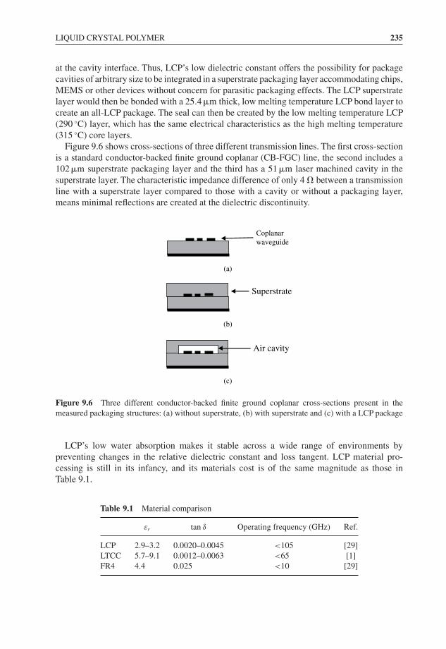
LIQUID CRYSTAL POLYMER 235
at the cavity interface. Thus, LCP’s low dielectric constant offers the possibility for packagecavities of arbitrary size to be integrated in a superstrate packaging layer accommodating chips,MEMS or other devices without concern for parasitic packaging effects. The LCP superstratelayer would then be bonded with a 25.4 �m thick, low melting temperature LCP bond layer tocreate an all-LCP package. The seal can then be created by the low melting temperature LCP(290 ◦C) layer, which has the same electrical characteristics as the high melting temperature(315 ◦C) core layers.
Figure 9.6 shows cross-sections of three different transmission lines. The first cross-sectionis a standard conductor-backed finite ground coplanar (CB-FGC) line, the second includes a102 �m superstrate packaging layer and the third has a 51 �m laser machined cavity in thesuperstrate layer. The characteristic impedance difference of only 4 � between a transmissionline with a superstrate layer compared to those with a cavity or without a packaging layer,means minimal reflections are created at the dielectric discontinuity.
(a)
(b)
(c)
Superstrate
Air cavity
Coplanarwaveguide
Figure 9.6 Three different conductor-backed finite ground coplanar cross-sections present in themeasured packaging structures: (a) without superstrate, (b) with superstrate and (c) with a LCP package
LCP’s low water absorption makes it stable across a wide range of environments bypreventing changes in the relative dielectric constant and loss tangent. LCP material pro-cessing is still in its infancy, and its materials cost is of the same magnitude as those inTable 9.1.
Table 9.1 Material comparison
εr tan δ Operating frequency (GHz) Ref.
LCP 2.9–3.2 0.0020–0.0045 <105 [29]LTCC 5.7–9.1 0.0012–0.0063 <65 [1]FR4 4.4 0.025 <10 [29]
236 ADVANCED ANTENNA MATERIALS
However, due to the capability of LCP to be handled by reel-to-reel processing, it is expectedthat production costs will continue to fall. At the same time, the material’s flexibility andrelatively low processing temperatures make it suitable for applications such as conformalantenna arrays, and for the integration of microelectromechanical system (MEMS) devices,such as low-loss RF switches.
As will be realised from the above, multilayer LCP circuits are feasible due to the materialfeatures of different melting temperatures. High melting temperature LCP (315 ◦C) can beused for core layers, while low melting temperature LCP (290 ◦C) is used as a bond ply. Thus,vertically integrated designs may be realised that are similar to those in LTCC. An additionalbenefit in multilayer LCPfabrication is the functionality provided by the low dielectric constant.This is useful for vertically integrated designs where the antenna is printed on the top layer ofan all-LCP module.
The fabrication difficulties of LCP have been solved gradually over the years [30–37].A biaxial die extrusion process was developed [19, 25] that solved the tearing problems bygiving the material uniform strength and it also created additional processing benefits. It wasdiscovered that by controlling the angle and rate of LCP extrusion through the biaxial die, thexy coefficient of thermal expansion (CTE) could be controlled to between approximately 0 and40 ppm/◦C. Thus, by this process a thermal expansion match in the xy plane can be achievedwith many commonly used materials.
LCP’s z axis CTE is considerably higher, ∼ 105 ppm/◦C , but due to the thin layers ofLCP used, the absolute z dimension difference between LCP and a 51 �m high copper platedthrough holes, is less than one of a half-micrometre within a ±100◦C temperature range [38].This makes z axis expansion a minimal concern until very thick multilayer modules come intoconsideration.
Since 2002, many of the LCP process limitations had been overcome [39], and it becamecommercially available in thin films with single and double copper cladding. Interest has grownquickly in utilising LCP for higher-frequency applications [40, 41]. Many publications [42, 43]have reported microwave characterization of LCP using microstrip ring resonators of up to34.5 GHz. Additionally, a 50 � conductor-backed coplanar waveguide (CB-CPW) transmis-sion line on LCP [44], has shown LCP to have low loss from 2 to 110 GHz, and a coplanarwaveguide (CPW) on LCP [45] has been measured to 50 GHz.
However, achieving broadband dielectric material characterisation at higher frequencies isnot a trivial task. The ring resonator (see Figure 9.7) provides dielectric information at discretefrequency points at periodic resonant peaks, but substrate thickness, ring diameter and thedielectric constant of the material under test all affect the accuracy of the measurement. Inaddition, at high frequencies where the skin depth approaches the characteristic dimension ofthe surface roughness of the resonator’s metal lines, it becomes difficult to separate the effectsof the conductor from dielectric losses.
Figure 9.7 Ring resonator
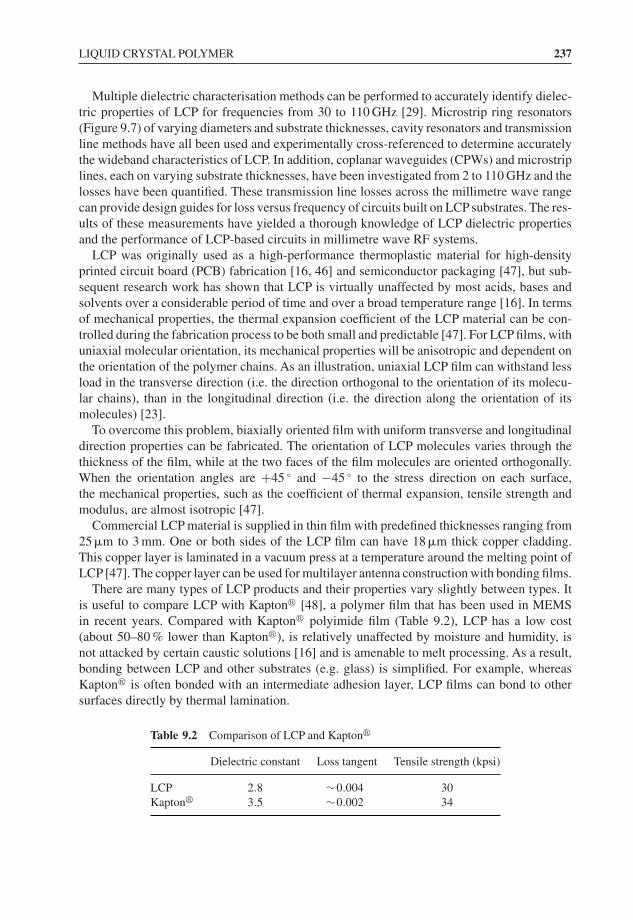
LIQUID CRYSTAL POLYMER 237
Multiple dielectric characterisation methods can be performed to accurately identify dielec-tric properties of LCP for frequencies from 30 to 110 GHz [29]. Microstrip ring resonators(Figure 9.7) of varying diameters and substrate thicknesses, cavity resonators and transmissionline methods have all been used and experimentally cross-referenced to determine accuratelythe wideband characteristics of LCP. In addition, coplanar waveguides (CPWs) and microstriplines, each on varying substrate thicknesses, have been investigated from 2 to 110 GHz and thelosses have been quantified. These transmission line losses across the millimetre wave rangecan provide design guides for loss versus frequency of circuits built on LCP substrates. The res-ults of these measurements have yielded a thorough knowledge of LCP dielectric propertiesand the performance of LCP-based circuits in millimetre wave RF systems.
LCP was originally used as a high-performance thermoplastic material for high-densityprinted circuit board (PCB) fabrication [16, 46] and semiconductor packaging [47], but sub-sequent research work has shown that LCP is virtually unaffected by most acids, bases andsolvents over a considerable period of time and over a broad temperature range [16]. In termsof mechanical properties, the thermal expansion coefficient of the LCP material can be con-trolled during the fabrication process to be both small and predictable [47]. For LCP films, withuniaxial molecular orientation, its mechanical properties will be anisotropic and dependent onthe orientation of the polymer chains. As an illustration, uniaxial LCP film can withstand lessload in the transverse direction (i.e. the direction orthogonal to the orientation of its molecu-lar chains), than in the longitudinal direction (i.e. the direction along the orientation of itsmolecules) [23].
To overcome this problem, biaxially oriented film with uniform transverse and longitudinaldirection properties can be fabricated. The orientation of LCP molecules varies through thethickness of the film, while at the two faces of the film molecules are oriented orthogonally.When the orientation angles are +45 ◦ and −45 ◦ to the stress direction on each surface,the mechanical properties, such as the coefficient of thermal expansion, tensile strength andmodulus, are almost isotropic [47].
Commercial LCP material is supplied in thin film with predefined thicknesses ranging from25 �m to 3 mm. One or both sides of the LCP film can have 18 �m thick copper cladding.This copper layer is laminated in a vacuum press at a temperature around the melting point ofLCP [47]. The copper layer can be used for multilayer antenna construction with bonding films.
There are many types of LCP products and their properties vary slightly between types. Itis useful to compare LCP with Kapton� [48], a polymer film that has been used in MEMSin recent years. Compared with Kapton� polyimide film (Table 9.2), LCP has a low cost(about 50–80 % lower than Kapton�), is relatively unaffected by moisture and humidity, isnot attacked by certain caustic solutions [16] and is amenable to melt processing. As a result,bonding between LCP and other substrates (e.g. glass) is simplified. For example, whereasKapton� is often bonded with an intermediate adhesion layer, LCP films can bond to othersurfaces directly by thermal lamination.
Table 9.2 Comparison of LCP and Kapton�
Dielectric constant Loss tangent Tensile strength (kpsi)
LCP 2.8 ∼0.004 30Kapton� 3.5 ∼0.002 34
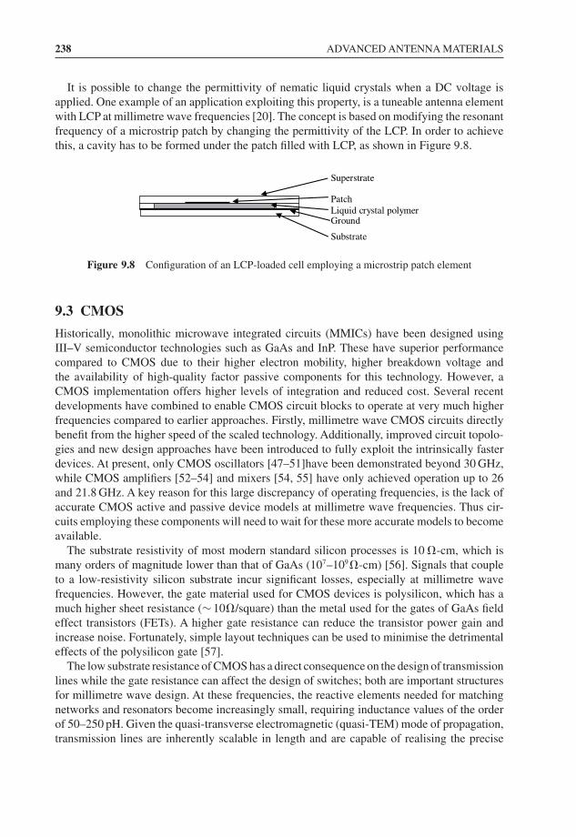
238 ADVANCED ANTENNA MATERIALS
It is possible to change the permittivity of nematic liquid crystals when a DC voltage isapplied. One example of an application exploiting this property, is a tuneable antenna elementwith LCP at millimetre wave frequencies [20]. The concept is based on modifying the resonantfrequency of a microstrip patch by changing the permittivity of the LCP. In order to achievethis, a cavity has to be formed under the patch filled with LCP, as shown in Figure 9.8.
Superstrate
Patch Liquid crystal polymerGround
Substrate
Figure 9.8 Configuration of an LCP-loaded cell employing a microstrip patch element
9.3 CMOS
Historically, monolithic microwave integrated circuits (MMICs) have been designed usingIII–V semiconductor technologies such as GaAs and InP. These have superior performancecompared to CMOS due to their higher electron mobility, higher breakdown voltage andthe availability of high-quality factor passive components for this technology. However, aCMOS implementation offers higher levels of integration and reduced cost. Several recentdevelopments have combined to enable CMOS circuit blocks to operate at very much higherfrequencies compared to earlier approaches. Firstly, millimetre wave CMOS circuits directlybenefit from the higher speed of the scaled technology. Additionally, improved circuit topolo-gies and new design approaches have been introduced to fully exploit the intrinsically fasterdevices. At present, only CMOS oscillators [47–51]have been demonstrated beyond 30 GHz,while CMOS amplifiers [52–54] and mixers [54, 55] have only achieved operation up to 26and 21.8 GHz. A key reason for this large discrepancy of operating frequencies, is the lack ofaccurate CMOS active and passive device models at millimetre wave frequencies. Thus cir-cuits employing these components will need to wait for these more accurate models to becomeavailable.
The substrate resistivity of most modern standard silicon processes is 10 �-cm, which ismany orders of magnitude lower than that of GaAs (107–109�-cm) [56]. Signals that coupleto a low-resistivity silicon substrate incur significant losses, especially at millimetre wavefrequencies. However, the gate material used for CMOS devices is polysilicon, which has amuch higher sheet resistance (∼ 10�/square) than the metal used for the gates of GaAs fieldeffect transistors (FETs). A higher gate resistance can reduce the transistor power gain andincrease noise. Fortunately, simple layout techniques can be used to minimise the detrimentaleffects of the polysilicon gate [57].
The low substrate resistance of CMOS has a direct consequence on the design of transmissionlines while the gate resistance can affect the design of switches; both are important structuresfor millimetre wave design. At these frequencies, the reactive elements needed for matchingnetworks and resonators become increasingly small, requiring inductance values of the orderof 50–250 pH. Given the quasi-transverse electromagnetic (quasi-TEM) mode of propagation,transmission lines are inherently scalable in length and are capable of realising the precise
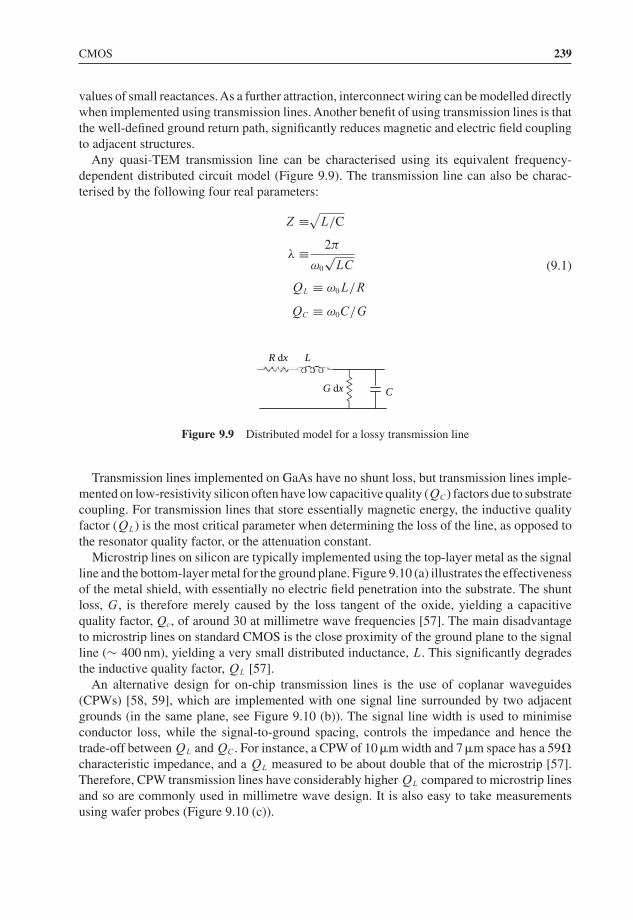
CMOS 239
values of small reactances.As a further attraction, interconnect wiring can be modelled directlywhen implemented using transmission lines. Another benefit of using transmission lines is thatthe well-defined ground return path, significantly reduces magnetic and electric field couplingto adjacent structures.
Any quasi-TEM transmission line can be characterised using its equivalent frequency-dependent distributed circuit model (Figure 9.9). The transmission line can also be charac-terised by the following four real parameters:
Z ≡√L/C
λ ≡ 2π
ω0
√LC
QL ≡ ω0L/R
QC ≡ ω0C/G
(9.1)
R dx L
G dx C
Figure 9.9 Distributed model for a lossy transmission line
Transmission lines implemented on GaAs have no shunt loss, but transmission lines imple-mented on low-resistivity silicon often have low capacitive quality (QC) factors due to substratecoupling. For transmission lines that store essentially magnetic energy, the inductive qualityfactor (QL) is the most critical parameter when determining the loss of the line, as opposed tothe resonator quality factor, or the attenuation constant.
Microstrip lines on silicon are typically implemented using the top-layer metal as the signalline and the bottom-layer metal for the ground plane. Figure 9.10 (a) illustrates the effectivenessof the metal shield, with essentially no electric field penetration into the substrate. The shuntloss, G, is therefore merely caused by the loss tangent of the oxide, yielding a capacitivequality factor, Qc, of around 30 at millimetre wave frequencies [57]. The main disadvantageto microstrip lines on standard CMOS is the close proximity of the ground plane to the signalline (∼ 400 nm), yielding a very small distributed inductance, L. This significantly degradesthe inductive quality factor, QL [57].
An alternative design for on-chip transmission lines is the use of coplanar waveguides(CPWs) [58, 59], which are implemented with one signal line surrounded by two adjacentgrounds (in the same plane, see Figure 9.10 (b)). The signal line width is used to minimiseconductor loss, while the signal-to-ground spacing, controls the impedance and hence thetrade-off between QL and QC . For instance, a CPW of 10 �m width and 7 �m space has a 59�characteristic impedance, and a QL measured to be about double that of the microstrip [57].Therefore, CPW transmission lines have considerably higher QL compared to microstrip linesand so are commonly used in millimetre wave design. It is also easy to take measurementsusing wafer probes (Figure 9.10 (c)).
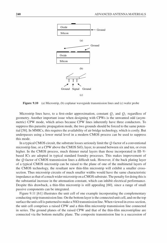
240 ADVANCED ANTENNA MATERIALS
(a)
Silicon
OxideGround
(b)
Silicon
Oxide
Ground
(c)
Ground Signal Ground
Figure 9.10 (a) Microstrip, (b) coplanar waveguide transmission lines and (c) wafer probe
Microstrip lines have, to a first-order approximation, constant QL and QC regardless ofgeometry. Another important issue when designing with CPWs is the unwanted odd (asym-metric) CPW mode, which arises because CPW lines inherently have three conductors. Tosuppress this parasitic propagation mode, the two grounds should be forced to the same poten-tial [58]. In MMICs, this requires the availability of air bridge technology, which is costly. Butunderpasses using a lower metal level in a modern CMOS process can be used to suppressthis mode.
In a typical CMOS circuit, the substrate losses seriously limit the Q-factor of a conventionalmicrostrip line, or a CPW above the CMOS SiO2 layer, to around between six and ten, or evenhigher. In the CMOS process, much thinner metal layers than those incorporated in III–V-based ICs are adopted in typical standard foundry processes. This makes improvement ofthe Q-factor of CMOS transmission lines a difficult task. However, if the back plating layerof a typical CMOS microstrip can be raised to the plane of one of the multimetal layers ofthe CMOS technology, the resultant new thin-film microstrip will exhibit a smaller cross-section. Thus microstrip circuits of much smaller widths would have the same characteristicimpedance as that of a much wider microstrip on a CMOS substrate. The penalty for doing this isthe substantial increase in the attenuation constant, which can inhibit electrical performance.Despite this drawback, a thin-film microstrip is still appealing [60], since a range of smallpassive components can be integrated.
Figure 9.11 [61] illustrates the unit cell of one example incorporating the complementaryconducting strip transmission line. On the bottom layer is the connected unit cell, and on the topsurface the unit cell is patterned to make a 50� transmission line. When viewed in cross-section,the unit cell comprises a raised CPW and a thin-film microstrip transmission line connectedin series. The ground planes of the raised CPW and that of the thin-film microstripline areconnected via the bottom metallic plane. The composite transmission line is a succession of
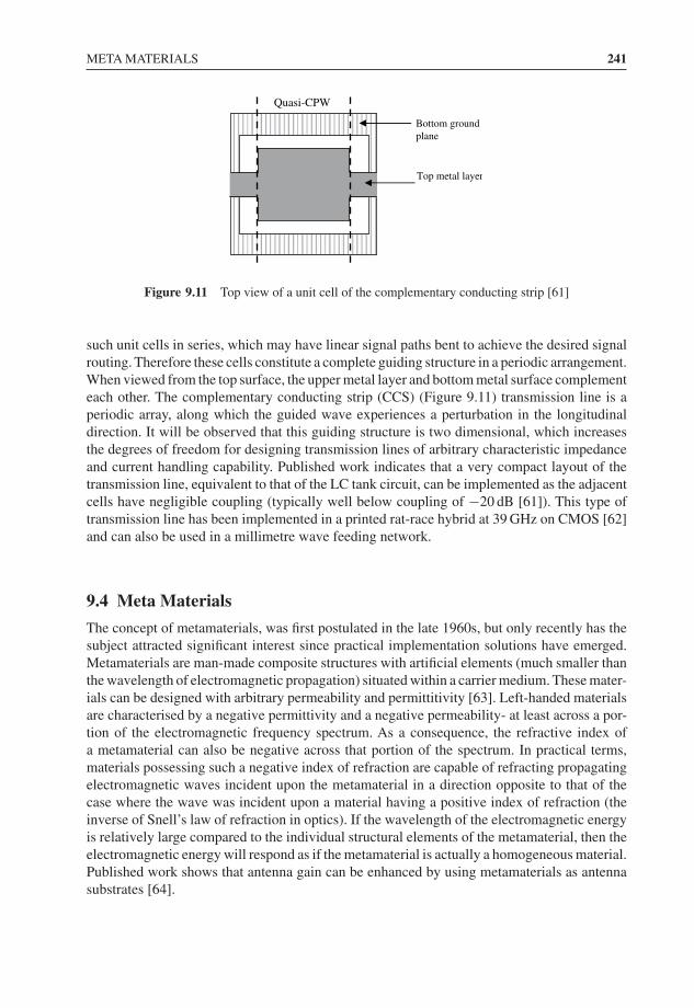
META MATERIALS 241
Bottom groundplane
Top metal layer
Quasi-CPW
Figure 9.11 Top view of a unit cell of the complementary conducting strip [61]
such unit cells in series, which may have linear signal paths bent to achieve the desired signalrouting. Therefore these cells constitute a complete guiding structure in a periodic arrangement.When viewed from the top surface, the upper metal layer and bottom metal surface complementeach other. The complementary conducting strip (CCS) (Figure 9.11) transmission line is aperiodic array, along which the guided wave experiences a perturbation in the longitudinaldirection. It will be observed that this guiding structure is two dimensional, which increasesthe degrees of freedom for designing transmission lines of arbitrary characteristic impedanceand current handling capability. Published work indicates that a very compact layout of thetransmission line, equivalent to that of the LC tank circuit, can be implemented as the adjacentcells have negligible coupling (typically well below coupling of −20 dB [61]). This type oftransmission line has been implemented in a printed rat-race hybrid at 39 GHz on CMOS [62]and can also be used in a millimetre wave feeding network.
9.4 Meta Materials
The concept of metamaterials, was first postulated in the late 1960s, but only recently has thesubject attracted significant interest since practical implementation solutions have emerged.Metamaterials are man-made composite structures with artificial elements (much smaller thanthe wavelength of electromagnetic propagation) situated within a carrier medium. These mater-ials can be designed with arbitrary permeability and permittitivity [63]. Left-handed materialsare characterised by a negative permittivity and a negative permeability- at least across a por-tion of the electromagnetic frequency spectrum. As a consequence, the refractive index ofa metamaterial can also be negative across that portion of the spectrum. In practical terms,materials possessing such a negative index of refraction are capable of refracting propagatingelectromagnetic waves incident upon the metamaterial in a direction opposite to that of thecase where the wave was incident upon a material having a positive index of refraction (theinverse of Snell’s law of refraction in optics). If the wavelength of the electromagnetic energyis relatively large compared to the individual structural elements of the metamaterial, then theelectromagnetic energy will respond as if the metamaterial is actually a homogeneous material.Published work shows that antenna gain can be enhanced by using metamaterials as antennasubstrates [64].
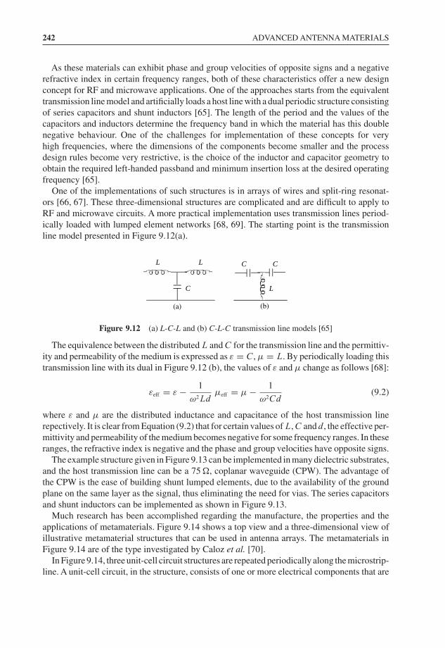
242 ADVANCED ANTENNA MATERIALS
As these materials can exhibit phase and group velocities of opposite signs and a negativerefractive index in certain frequency ranges, both of these characteristics offer a new designconcept for RF and microwave applications. One of the approaches starts from the equivalenttransmission line model and artificially loads a host line with a dual periodic structure consistingof series capacitors and shunt inductors [65]. The length of the period and the values of thecapacitors and inductors determine the frequency band in which the material has this doublenegative behaviour. One of the challenges for implementation of these concepts for veryhigh frequencies, where the dimensions of the components become smaller and the processdesign rules become very restrictive, is the choice of the inductor and capacitor geometry toobtain the required left-handed passband and minimum insertion loss at the desired operatingfrequency [65].
One of the implementations of such structures is in arrays of wires and split-ring resonat-ors [66, 67]. These three-dimensional structures are complicated and are difficult to apply toRF and microwave circuits. A more practical implementation uses transmission lines period-ically loaded with lumped element networks [68, 69]. The starting point is the transmissionline model presented in Figure 9.12(a).
(a) (b)
LC
C CL L
Figure 9.12 (a) L-C-L and (b) C-L-C transmission line models [65]
The equivalence between the distributed L and C for the transmission line and the permittiv-ity and permeability of the medium is expressed as ε = C, μ = L. By periodically loading thistransmission line with its dual in Figure 9.12 (b), the values of ε and μ change as follows [68]:
εeff = ε − 1
ω2Ldμeff = μ − 1
ω2Cd(9.2)
where ε and μ are the distributed inductance and capacitance of the host transmission linerepectively. It is clear from Equation (9.2) that for certain values of L, C and d, the effective per-mittivity and permeability of the medium becomes negative for some frequency ranges. In theseranges, the refractive index is negative and the phase and group velocities have opposite signs.
The example structure given in Figure 9.13 can be implemented in many dielectric substrates,and the host transmission line can be a 75 �, coplanar waveguide (CPW). The advantage ofthe CPW is the ease of building shunt lumped elements, due to the availability of the groundplane on the same layer as the signal, thus eliminating the need for vias. The series capacitorsand shunt inductors can be implemented as shown in Figure 9.13.
Much research has been accomplished regarding the manufacture, the properties and theapplications of metamaterials. Figure 9.14 shows a top view and a three-dimensional view ofillustrative metamaterial structures that can be used in antenna arrays. The metamaterials inFigure 9.14 are of the type investigated by Caloz et al. [70].
In Figure 9.14, three unit-cell circuit structures are repeated periodically along the microstrip-line. A unit-cell circuit, in the structure, consists of one or more electrical components that are
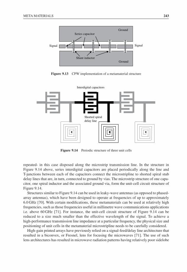
META MATERIALS 243
Series capacitor
Shunt inductorGround
Ground
Signal Signal
Figure 9.13 CPW implementation of a metamaterial structure
Interdigital capacitors
Shorted spiraldelay line
Figure 9.14 Periodic structure of three unit cells
repeated- in this case disposed along the microstrip transmission line. In the structure inFigure 9.14 above, series interdigital capacitors are placed periodically along the line andT-junctions between each of the capacitors connect the microstripline to shorted spiral stubdelay lines that are, in turn, connected to ground by vias. The microstrip structure of one capa-citor, one spiral inductor and the associated ground via, form the unit-cell circuit structure ofFigure 9.14.
Structures similar to Figure 9.14 can be used in leaky-wave antennas (as opposed to phased-array antennas), which have been designed to operate at frequencies of up to approximately6.0 GHz [70]. With certain modifications, these metamaterials can be used at relatively highfrequencies, such as those frequencies useful in millimetre wave communications applicationsi.e. above 60 GHz [71]. For instance, the unit-cell circuit structure of Figure 9.14 can bereduced to a size much smaller than the effective wavelength of the signal. To achieve ahigh-performance transmission line impedance at a particular frequency, the physical size andpositioning of unit cells in the metamaterial microstripline needs to be carefully considered.
High-gain printed arrays have previously relied on a signal-feed/delay line architecture thatresulted in a biconvex, or Fresnel, lens for focusing the microwaves [71]. The use of suchlens architectures has resulted in microwave radiation patterns having relatively poor sidelobe
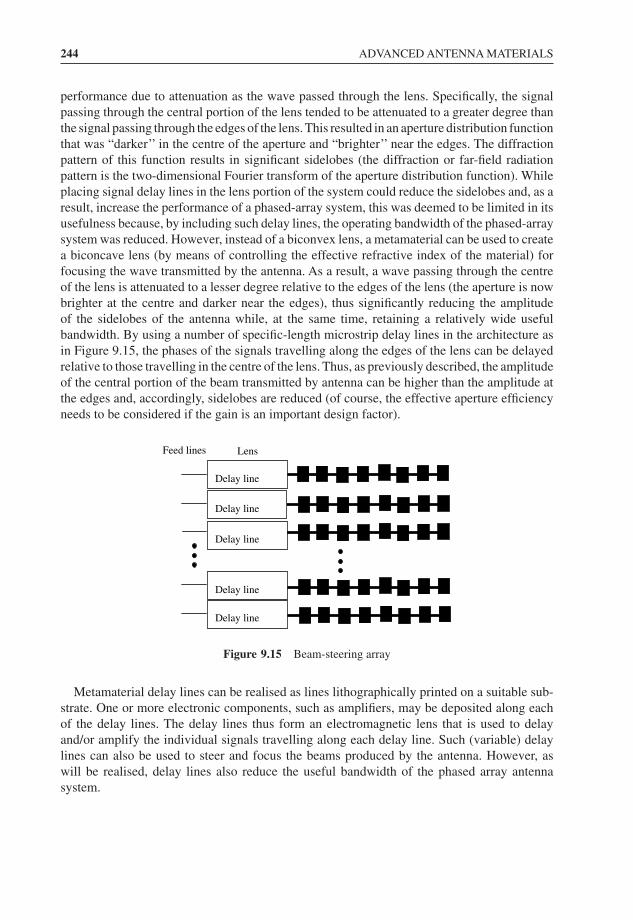
244 ADVANCED ANTENNA MATERIALS
performance due to attenuation as the wave passed through the lens. Specifically, the signalpassing through the central portion of the lens tended to be attenuated to a greater degree thanthe signal passing through the edges of the lens. This resulted in an aperture distribution functionthat was “darker’’ in the centre of the aperture and “brighter’’ near the edges. The diffractionpattern of this function results in significant sidelobes (the diffraction or far-field radiationpattern is the two-dimensional Fourier transform of the aperture distribution function). Whileplacing signal delay lines in the lens portion of the system could reduce the sidelobes and, as aresult, increase the performance of a phased-array system, this was deemed to be limited in itsusefulness because, by including such delay lines, the operating bandwidth of the phased-arraysystem was reduced. However, instead of a biconvex lens, a metamaterial can be used to createa biconcave lens (by means of controlling the effective refractive index of the material) forfocusing the wave transmitted by the antenna. As a result, a wave passing through the centreof the lens is attenuated to a lesser degree relative to the edges of the lens (the aperture is nowbrighter at the centre and darker near the edges), thus significantly reducing the amplitudeof the sidelobes of the antenna while, at the same time, retaining a relatively wide usefulbandwidth. By using a number of specific-length microstrip delay lines in the architecture asin Figure 9.15, the phases of the signals travelling along the edges of the lens can be delayedrelative to those travelling in the centre of the lens. Thus, as previously described, the amplitudeof the central portion of the beam transmitted by antenna can be higher than the amplitude atthe edges and, accordingly, sidelobes are reduced (of course, the effective aperture efficiencyneeds to be considered if the gain is an important design factor).
Feed lines
Delay line
Delay line
Delay line
Delay line
Delay line
Lens
Figure 9.15 Beam-steering array
Metamaterial delay lines can be realised as lines lithographically printed on a suitable sub-strate. One or more electronic components, such as amplifiers, may be deposited along eachof the delay lines. The delay lines thus form an electromagnetic lens that is used to delayand/or amplify the individual signals travelling along each delay line. Such (variable) delaylines can also be used to steer and focus the beams produced by the antenna. However, aswill be realised, delay lines also reduce the useful bandwidth of the phased array antennasystem.
HIGH-TEMPERATURE SUPERCONDUCTING ANTENNA 245
9.5 High-Temperature Superconducting Antenna
High-temperature superconducting antennas can exhibit an increase in overall gain comparedto their copper equivalent [72]. Many designs have been published and structures realised, asmicrostrip arrays directly corresponds to the conventional copper designs. At millimetre wavefrequencies, transmission line loss is important in determining the feasibility of an antennaarray. When a resonant array employs a corporate feed network, an additional effective pathlength is introduced so the actual loss will unavoidably increase. Travelling wave arrays haveshorter effective path lengths than resonant arrays and can appear to offer less loss. In a realimplementation for waveguide arrays, however, the actual loss will be greater, due to surfaceroughness, metal imperfections, etc. Use of superconducting waveguides can allow the effi-ciency of the feed component of the antenna to approach 0 dB, and thus may allow a significantextension of array techniques. For a printed array, it has been reported that a microstrip of con-ventional dimensions experiences a loss reduction of the order of 20 dB at 100 GHz, while athin-film microstrip realisation could show another 10 dB of loss reduction [73]. Thus withthe reduction in resistive loss associated with superconductors, high-gain microstrip arraysbecome a practical proposition at millimetre wave frequencies.
The use of high-temperature superconductor (HTS) thin-film structures in microwave integ-rated circuits employed in aerospace applications and terrestrial mobile communication basestations, offers the possibility of significantly reducing the weight and volume of the microwaveequipment, even though the system must include cryogenic equipment to provide an opera-tional temperature in the range of 60 to 77 K. Thus it can be said that the HTS applications inmicrowave engineering have become part of common industrial practice [74]. This emphas-izes the importance of investigation into the physical properties of HTS thin films and of thedevelopment of microwave characteristics of such films. Thin HTS films are prepared by epi-taxial growth on single-crystal dielectric substrates. In many cases, the film quality is governedto a considerable extent by the processes occurring at the interface between the film and thesubstrate. As a consequence, the state of the interface in heteroepitaxial systems consistingof HTS films and dielectric substrates becomes extremely important from the standpoint ofpractical applications of HTS in modern microwave electronics [74].
Superconductivity was initially discovered in 1911 and the highest superconducting trans-ition temperature observed was in the Nb3Ge compound (23.2 K), and this was the highesttransition temperature known of until 1986, when high-temperature superconductivity in theLa–Ba–Cu–O ceramic was announced. Before high-temperature superconductivity had beenestablished to exist, oxide-type superconductors were considered a curiosity and not worthyof serious consideration.
At the beginning of 1987, the situation changed abruptly, and the HTS became a subjectof worldwide interest. Figure 9.16 depicts the history of high-temperature superconductorsin terms of the compounds and their superconducting transition temperature. As the ini-tial interest gradually abated, the area of HTS applications has become the major focus ofresearch. Although the detailed physics of high-temperature superconductors differs fromthat of the earlier (low-temperature) superconductors, they nevertheless possess many of theproperties that are of interest to many applications in engineering. The YBa2Cu3O7−x andTl2Ba2Ca2Cu3O10 compounds deposited as thin films were found suitable for practical applic-ations as a basis for microwave devices [75, 76], with transition temperatures relatively easilyattained, both in the laboratory and in the field, for commercial applications.
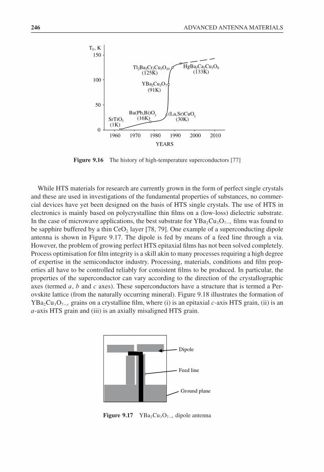
246 ADVANCED ANTENNA MATERIALS
YEARS
1960 1970 1980 1990 2000 2010
Tc, K
0
50
100
150
SrTiO3(1K)
Ba(Pb,Bi)O3
(16K)(La,Sr)CuO
3(30K)
YBa2Cu3O7(91K)
Tl2Ba2Cr2Cu3O10(125K)
HgBa2Ca2Cu3O8(133K)
Figure 9.16 The history of high-temperature superconductors [77]
While HTS materials for research are currently grown in the form of perfect single crystalsand these are used in investigations of the fundamental properties of substances, no commer-cial devices have yet been designed on the basis of HTS single crystals. The use of HTS inelectronics is mainly based on polycrystalline thin films on a (low-loss) dielectric substrate.In the case of microwave applications, the best substrate for YBa2Cu3O7−x films was found tobe sapphire buffered by a thin CeO2 layer [78, 79]. One example of a superconducting dipoleantenna is shown in Figure 9.17. The dipole is fed by means of a feed line through a via.However, the problem of growing perfect HTS epitaxial films has not been solved completely.Process optimisation for film integrity is a skill akin to many processes requiring a high degreeof expertise in the semiconductor industry. Processing, materials, conditions and film prop-erties all have to be controlled reliably for consistent films to be produced. In particular, theproperties of the superconductor can vary according to the direction of the crystallographicaxes (termed a, b and c axes). These superconductors have a structure that is termed a Per-ovskite lattice (from the naturally occurring mineral). Figure 9.18 illustrates the formation ofYBa2Cu3O7−x grains on a crystalline film, where (i) is an epitaxial c-axis HTS grain, (ii) is ana-axis HTS grain and (iii) is an axially misaligned HTS grain.
Dipole
Feed line
Ground plane
Figure 9.17 YBa2Cu3O7−x dipole antenna
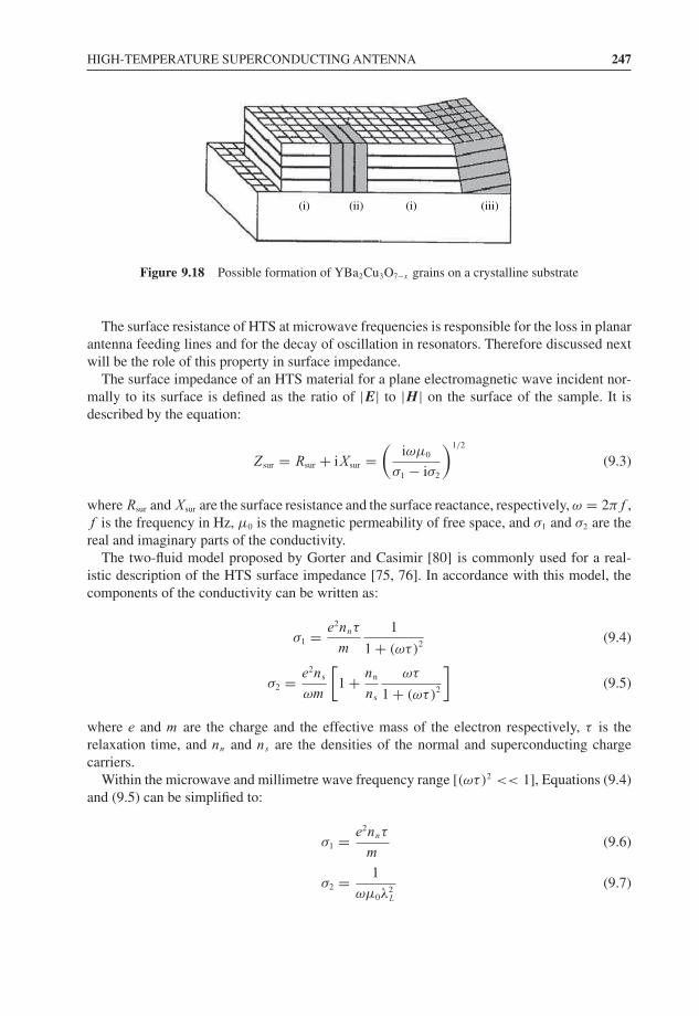
HIGH-TEMPERATURE SUPERCONDUCTING ANTENNA 247
(i) (ii) (i) (iii)
Figure 9.18 Possible formation of YBa2Cu3O7−x grains on a crystalline substrate
The surface resistance of HTS at microwave frequencies is responsible for the loss in planarantenna feeding lines and for the decay of oscillation in resonators. Therefore discussed nextwill be the role of this property in surface impedance.
The surface impedance of an HTS material for a plane electromagnetic wave incident nor-mally to its surface is defined as the ratio of |E| to |H | on the surface of the sample. It isdescribed by the equation:
Zsur = Rsur + iXsur =(
iωμ0
σ1 − iσ2
)1/2
(9.3)
where Rsur and Xsur are the surface resistance and the surface reactance, respectively, ω = 2πf ,f is the frequency in Hz, μ0 is the magnetic permeability of free space, and σ1 and σ2 are thereal and imaginary parts of the conductivity.
The two-fluid model proposed by Gorter and Casimir [80] is commonly used for a real-istic description of the HTS surface impedance [75, 76]. In accordance with this model, thecomponents of the conductivity can be written as:
σ1 = e2nnτ
m
1
1 + (ωτ)2 (9.4)
σ2 = e2ns
ωm
[1 + nn
ns
ωτ
1 + (ωτ)2
](9.5)
where e and m are the charge and the effective mass of the electron respectively, τ is therelaxation time, and nn and ns are the densities of the normal and superconducting chargecarriers.
Within the microwave and millimetre wave frequency range [(ωτ)2 << 1], Equations (9.4)and (9.5) can be simplified to:
σ1 = e2nnτ
m(9.6)
σ2 = 1
ωμ0λ2L
(9.7)
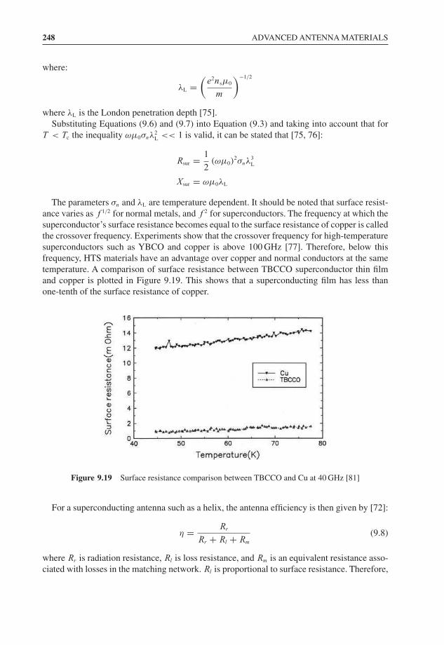
248 ADVANCED ANTENNA MATERIALS
where:
λL =(
e2nsμ0
m
)−1/2
where λL is the London penetration depth [75].Substituting Equations (9.6) and (9.7) into Equation (9.3) and taking into account that for
T < Tc the inequality ωμ0σnλ2L << 1 is valid, it can be stated that [75, 76]:
Rsur = 1
2(ωμ0)
2σnλ3L
Xsur = ωμ0λL
The parameters σn and λL are temperature dependent. It should be noted that surface resist-ance varies as f 1/2 for normal metals, and f 2 for superconductors. The frequency at which thesuperconductor’s surface resistance becomes equal to the surface resistance of copper is calledthe crossover frequency. Experiments show that the crossover frequency for high-temperaturesuperconductors such as YBCO and copper is above 100 GHz [77]. Therefore, below thisfrequency, HTS materials have an advantage over copper and normal conductors at the sametemperature. A comparison of surface resistance between TBCCO superconductor thin filmand copper is plotted in Figure 9.19. This shows that a superconducting film has less thanone-tenth of the surface resistance of copper.
Figure 9.19 Surface resistance comparison between TBCCO and Cu at 40 GHz [81]
For a superconducting antenna such as a helix, the antenna efficiency is then given by [72]:
η = Rr
Rr + Rl + Rm
(9.8)
where Rr is radiation resistance, Rl is loss resistance, and Rm is an equivalent resistance asso-ciated with losses in the matching network. Rl is proportional to surface resistance. Therefore,
REFERENCES 249
antenna efficiency can be improved as the surface resistance is reduced, and superconductingantennas could have better efficiency than copper antennas at the same temperature.
In addition to millimetre wave antenna elements, high-temperature superconductors canalso be applied to superior-performance millimetre wave feeding networks, millimetre waveresonators and interconnects. The use of high dielectric constant substrates also means thatcomponents at these high frequencies can be considerably smaller than in conventional circuits.Metamaterial components can also be realised, and bulk components have begun to appearas research subjects. The advantages of high-temperature superconductors in millimetre waveapplications of up to 100 GHz are many, and although early commercial products at microwavefrequencies exist (e.g. in cellular base stations), the investigation into the use of these materialsat these higher frequencies remains a laboratory activity.
9.6 Nano Antennas
Nanotubes have different characteristics from conventional metallic transmission lines. Forinstance, the wave velocity on a carbon nanotube transmission line in free space is of theorder of the Fermi velocity vF, rather than the speed of light c. For a carbon nanotube, vF isabout 9.71 × 10⁵ m/s. It is found that the propagation velocity on a carbon nanotube dipole isvp ≈ 6.2vF ≈ 0.02c. Thus, wavelengths are much shorter in a carbon nanotube, compared tothose in a conventional microscopic metallic tube.
Basic properties of dipole transmitting antennas formed by carbon nanotubes have beenstudied [82]. Some properties of carbon nanotube antennas are found to be quite differentfrom the case of an infinitely thin copper antenna of the same size and shape. It is found thatcarbon nanotube antennas have plasmon resonances above a critical frequency, have high inputimpedances (which can be used for connecting to nanoelectronic circuits), and have very lowefficiencies.
A model for parallel wire carbon nanotube transmission lines has been created [83]. Surfacewaves on carbon nanotubes and carbon nanotube antennas are discussed there. Using carbonnanotubes, slow-wave structures with a wave velocity reduction of two orders of magnitudecan be realised. This opens up the potential for ultra-compact resonant antennas and extremelysmall distributed circuits, e.g. surface wave filters for frequencies of GHz, and up into the THzrange [84].
References[1] A. Matsuzawa, RF-SoC – Expectations and Required Conditions’, IEEE Transactions on Microwave Theory
and Techniques, 50, January 2002, 245–253.[2] K. Lim, S. Pinel, M. F. Davis, A. Sutono, C.-H. Lee, D. Heo, A. Obatoynbo, J. Laskar, M. Tentzeris and
R. Tummala, ‘RF-SOP for Wireless Communications’, IEEE Microwave Magazine, 3, March 2002, 88–99.[3] T. Kutilainen, ‘Ceramic Interconnect Initiative. NextGen, LTCC’, ELMO, November 2005, http://www.
imaps.org/cii/[4] Young Chul Lee, Won-il Chang and Chul Soon Park, ‘Monolithic LTCC SiP Transmitter for 60GHz Wireless
Communication Terminals’, IEEE Transactions on Microwave Theory and Techniques, MTT-S, June 2005,1015–1018.
[5] K. Lim, S. Pinel, M. F. Davis, A. Sutono, C.-H. Lee, D. Heo, A. Obatoynbo, J. Laskar, E. M .Tentzeris andR. Tummala, ‘RFSystem-on-Package (SOP) for Wireless Communications’, IEEE Microwave Magazine, 3(1),March 2002, 88–99.

250 ADVANCED ANTENNA MATERIALS
[6] J. Lee, K. Lim, S. Pinel, G. DeJean, R. L. Li, C.-H. Lee, M. F. Davis, M. Tentzeris and J. Laskar, ‘AdvancedSystem-on-Package (SOP) Multilayer Architectures for RF/Wireless Systems up to Millimetre-Wave FrequencyBands’, Proceedings of the Asian Pacific Microwave Conference, Seoul, Korea, November 2003, pp. FA5_01.
[7] R. Lucero, W. Qutteneh,A. Pavio, D. Meyers and J. Estes, ‘Design of an LTCC Switch Diplexer Front-End Modulefor GSM/DCS/PCS Application’, IEEE Radio Frequency Integrated Circuit Symosium, Phoenix, Arizona, May2001, pp. 213–216.
[8] Keko, ‘LTCC Production’, Keko Equipment Newsletter, November 2003, No. 2, pp. 6–7.[9] Young Chul Lee and Chul Soon Park, ‘A Novel High-Q LTCC Stripline Resonator for Millimetre-Wave
Applications’, IEEE Microwave and Wireless Components Letters, 13(12), 2003, 499–504.[10] S. Maci, L. Borelli and L. Rossi, ‘Diffraction at the Edge of a Truncated Grounded Dielectric Slab’, IEEE
Transactions on Antennas and Propagation, 44, June 1996, 863–872.[11] D. Moongilan, ‘Grounding Optimization Techniques for Controlling Radiation and Crosstalk in Mixed Signal
PCBs’, Proceedings of the IEEE Electromagnetic Compatibility Symposium, 1, August 1998, 495–500.[12] G. DeJean, R. L. Li, M. M. Tentzeris, J. Papapolymerou and J. Laskar, ‘Radiation-Pattern Improvement of
Patch Antennas Using a Compact Soft/Hard Surface (SHS) Structure on LTCC Multilayer Technology’, IEEETransactions on Antennas and Propagation, AP-S, 2004, 317–320.
[13] George E. Ponchak, Donghoon Chun, Jong-Gwan Yook and Linda P. B. Katehi, ‘The Use of Metal Filled ViaHoles for Improving Isolation in LTCC RF and Wireless Multichip Packages’, IEEE Transactions on AdvancedPackaging, 23(1), February 2000, 88–99.
[14] Dane Thompson, Nickolas Kingsley, Guoan Wang, John Papapolymerou and Manos M. Tentzeris, ‘RF Char-acteristics of Thin Film Liquid Crystal Polymer (LCP) Packages for RF MEMS and MMIC Integration’, IEEETransactions on Microwave Theory and Techniques, MTT-S, June 2005.
[15] S. Pinel, M. Davis, V. Sundaram, K. Lim, J. Laskar, G. White and R. Tummala, ‘High Q Passives on Liquid CrystalPolymer Substrates and μBGA Technology for 3D Integrated RF Front-End Module’, IEICE Transactions onElectronics, E86-C(8), August 2003, 1584–1592.
[16] E. C. Culbertson, ‘A New Laminate Material for High Performance PCBs: Liquid Crystal Polymer Copper CladFilms’, Proceedings of the 45th Electronic Components and Technology Conference, 1995, pp 520–523.
[17] K. Jayaraj, T. E. Noll and D. R. Singh, ‘RF Characterization of a Low Cost Multichip Packaging Technologyfor Monolithic Microwave and Millimetre Wave Integrated Circuits’, URSI International Signals, Systems, andElectronics Symposium, October 1995, pp. 443–446.
[18] E. C. Culbertson, ‘A New Laminate Material for High Performance PCBs: Liquid Crystal Polymer Copper CladFilms’, IEEE Electronic Components and Technology Conference, May 1995, pp. 520–523.
[19] K. Jayaraj, T. E. Noll and D. R. Singh, ‘A Low Cost Multichip Packaging Technology for Monolithic MicrowaveIntegrated Circuits’, IEEE Transactions on Antennas and Propagation, 43, September 1995, 992–997.
[20] R. Marin, A. Mössinger, J. Freese, A. Manabe and R. Jakoby, ‘Realization of 35 GHz Steerable Reflectar-rays Using Highly Anisotropic Liquid Crystal’, IEEE Transactions on Antennas and Propagation, AP-S, 2006,4307–4310.
[21] L. Chorosinski, ‘Low Cost, Lightweight, Inflatable Antenna Array Development Using Flip Chip on FlexibleMembranes for Space-Based Radar Applications’, Northrop Grumman Company Report, 2000
[22] H. Inoue, S. Fukutake and H. Ohata, ‘Liquid Crystal Polymer Film Heat Resistance and High DimensionalStability, Proceedings of the Pan Pacific Microelectronics Symposium, February 2001, pp. 273–278.
[23] X. Wang, J. Engel and C. Liu, ‘Liquid Crystal Polymer (LCP) for MEMS: Processes and Applications’, Journalof Micromechanical Microengineering, 13, September 2003, 628–633.
[24] L. M. Higgins III, ‘Hermetic and Optoelectronic Packaging Concepts Using Multiplayer and Active PolymerSystems’, Advancing Microelectronics, 30(4), July/August 2003, 6–13.
[25] B. Farrell and M. St Lawrence, ‘The Processing of Liquid Crystalline Polymer Printed Circuits’, IEEE ElectronicComponents and Technology Conference, May 2002, pp. 667–671.
[26] G. Zou, H. Gronqvist, J. P. Starski and J. Liu, ‘Characterization of Liquid Crystal Polymer for High FrequencySystem-in-a-PackageApplications’, IEEE Transactions on Advanced Packaging, 25, , November 2002, 503–508.
[27] K. Gilleo, J. Belmonte and G. Pham-Van-Diep, ‘Low Ball BGA: A New Concept in Thermoplastic Packaging’,IEEE 29th International Electrical Manufacturing Technology Symposium, July 2004, pp. 345–354.
[28] R. J. Ross, ‘LCP Injection Molded Packages – Keys to JEDEC 1 Performance’, IEEE 54th ElectricalComputational Technology Conference, June 2004, pp. 1807–1811.

REFERENCES 251
[29] D. C. Thompson, O. Tantot, H. Jallageas, G. E. Ponchak, M. M. Tentzeris and J. Papapolymerou, ‘Characterizationof Liquid Crystal Polymer (LCP) Material and Transmission Lines on LCP Substrates from 30 to 110 GHz’, IEEETransactions on Microwave Theory and Techniques, 52, April 2004, 1343–1352.
[30] C. Khoo, B. Brox, R. Norrhede and F. Maurer, ‘Effect of Copper Lamination on the Rheological and CopperAdhe-sion Properties of a Thermotropic Liquid Crystalline Polymer Used in PCB Applications’, IEEE Transactionson Component Packaging and Manufacturing Technology, 20, July 1997, 219–226.
[31] T. Suga, A. Takahashi, K. Saijo and S. Oosawa, ‘New Fabrication Technology of Polymer/Metal Lamination andIts Application in Electronic Packaging’, IEEE 1st International Polymers and Adhesives in Microelectronicsand Photonics Conference, October 2001, pp. 29–34.
[32] X. Wang, L. Lu and C. Liu, ‘Micromachining Techniques for Liquid Crystal Polymer’, 14th IEEE InternationalMEMS Conference, January 2001, pp. 21–25.
[33] K. Brownlee, S. Bhattacharya, K. Shinotani, C. P. Wong and R. Tummala, ‘Liquid Crystal Polymers (LCP)for High Performance SOP Applications’, 8th International Advanced Packaging Materials Symposium, March2002, pp. 249–253.
[34] J. Kivilahti, J. Liu, J. E. Morris, T. Suga and C. P. Wong, ‘Panel-Size Component Integration (PCI) with MoldedLiquid Crystal Polymer (LCP) Substrates’, IEEE Electronic Components and Technology Conference, May2002, pp. 955–961.
[35] T. Suga,A. Takahashi, M. Howlander, K. Saijo and S. Oosawa, ‘ALamination Technique of LCP/Cu for ElectronicPackaging’, 2nd International IEEE Polymers andAdhesives in Microelectronics and Photonics Conference, June2002, pp. 177–182.
[36] T. Zhang, W. Johnson, B. Farrell and M. St Lawrence, ‘The Processing and Assembly of Liquid CrystallinePolymer Printed Circuits’, Proceedings of the International Society for Optical Engineering, 2002, 1–9.
[37] L. Chen, M. Crnic, L. Zonghe and J. Liu, ‘Process Development and Adhesion Behavior of Electroless Copperon Liquid Crystal Polymer (LCP) for Electronic Packaging Application’, IEEE Transactions on ElectronicsPackaging Manufacture, 25, October 2002, 273–278.
[38] Modern Machine Shop Online, http://www.mmsonline.com/articles/ 030107.html[39] PMTEC LCP Materials Symposium, Huntsville, Alabama, 29 October 2002.[40] H. Kanno, H. Ogura and K. Takahashi, ‘Surface Mountable Liquid Crystal Polymer Package with Vertical Via
Transition Compensating Wire Inductance up to V–Band’, IEEE MTT-S International Microwave SymposiumDigest, 2, June 2003, 1159–1162.
[41] M. F. Davis, S.-W. Yoon, S. Pinel, K. Lim and J. Laskar, ‘Liquid Crystal Polymer-Based Integrated PassiveDevelopment for RF Applications’, IEEE MTT-S International Microwave Symposium Digest, 2, June 2003,pp. 1155–1158.
[42] G. Zou, H. Gronqvist, P. Starski and J. Liu, ‘High Frequency Characteristics of Liquid Crystal Polymer forSystem in a Package Application’, IEEE 8th International Advanced Packaging Materials Symposium, March2002, pp. 337–341.
[43] G. Zou, H. Gronqvist, J. P. Starski and J. Liu, ‘Characterization of Liquid Crystal Polymer for High FrequencySystem-in-a-Package Applications’, IEEE Transactions on Advanced Packaging, 25, November 2002, 503–508.
[44] D. Thompson, P. Kirby, J. Papapolymerou and M. M. Tentzeris, ‘W-Band Characterization of Finite GroundCoplanar Transmission Lines on Liquid Crystal Polymer (LCP) Substrates’, IEEE Electronic ComponentsTechnology Conference, May 2003, pp. 1652–1655.
[45] Z.Wei and A. Pham, ‘Liquid Crystal Polymer (LCP) for Microwave/Millimetre Wave Multi-layer Packaging’,IEEE MTT-S International Microwave Symposium Digest, 3, June 2003, 2273–2276.
[46] C. G. L. Khoo, B. Brox, R. Norrhede and F. H. J. Maurer, ‘Effect of Copper Lamination on the Rheological andCopper Adhesion Properties of a Thermotropic Liquid Crystalline Polymer Used in PCB Applications’, IEEETransactions on Component Packaging and Manufacturing Technology, 20, 1997, 219–226.
[47] K. Jayaraj and B. Farrell, ‘Liquid Crystal Polymers and Their Role in Electronic Packaging’, AdvancingMicroelectronics, 1998, 15–18.
[48] Kapton� polymide film, http://www.dupont.com/[49] L. M. Franca-Neto, R. E. Bishop and B. A. Bloechel, ‘64 GHz and 100 GHz VCOs in 90 nm CMOS Using
Optimum Pumping Method’, IEEE International Solid-State Circuits Conference Digest Technical Papers,February 2004, pp. 444–445.
[50] R.-C. Liu, H.-Y. Chang, C.-H. Wang and H. Wang, ‘A 63 GHz VCO Using a Standard 0.25 um CMOS Process’,IEEE International Solid-State Circuits Conference Digest Technical Papers, February 2004, pp. 446–447.

252 ADVANCED ANTENNA MATERIALS
[51] M. Tiebout, H.-D. Wohlmuth and W. Simbürger, ‘A 1 V 51 GHz fully integrated VCO in 0.12 �m CMOS’, IEEEInternational Solid-State Circuits Conference Digest, February 2002, 238–239.
[52] K.-W. Yu, Y.-L. Lu, D.-C. Chang, V. Liang and M. F. Chang, ‘K-Band Low-Noise Amplifiers Using 0.18 �mCMOS Technology’, IEEE Microwave Wireless Component Letters, 14(3), March 2004, 106–108.
[53] L. M. Franca-Neto, B.A. Bloechel and K. Soumyanath, ‘17 GHz and 24 GHz LNADesigns Based on Extended-S-Parameter with Microstrip-on-Die in 0.18 �m Logic CMOS Technology’, Proceedings of European Solid-StateCircuits Conference, September 2003, 149–152.
[54] X. Guan and A. Hajimiri, ‘A 24 GHz CMOS Front-End’, Proceedings of European Solid-State CircuitsConference, September 2002, 155–158.
[55] M. Madihian, H. Fujii, H.Yoshida, H. Suzuki and T.Yamazaki, ‘A 1–10 GHz, 0.18 �m-CMOS Chipset for Multi-mode Wireless Applications’, IEEE MTT-S International Microwave Symposium Digest, June 2001, 1865–1868.
[56] I. Bahl and P. Bhartia, ‘Microwave Solid State Circuit Design’, 2nd edition, John Wiley & Sons, Inc., Hoboken,New Jersey, 2003.
[57] Chinh H. Doan, Sohrab Emami, Ali M. Niknejad and Robert W. Brodersen, ‘Millimetre-Wave CMOS Design’,IEEE Journal of Solid-State Circuits, 40(1), January 2005, 144–156.
[58] T. C. Edwards and M. B. Steer, ‘Foundations of Interconnect and Microstrip Design’, 3rd edition, John Wiley &Sons, Inc., New York, 2000.
[59] B. Kleveland, C. H. Diaz, D. Vook, L. Madden, T. H. Lee and S. S. Wong, ‘Exploiting CMOS Reverse InterconnectScaling in MultigigahertzAmplifier and Oscillator Design’, IEEE Journal of Solid-State Circuits, 36(10), October2001, 1480–1488.
[60] K. Nishikawa et al., ‘Miniaturized Millimetre-Wave Masterslice 3-D MMIC Amplifier and Mixer’, IEEE MTTTTransactions, 47(1), September 1999, 1856–1862.
[61] Ching-Kuang C. Tzuang, Chih-Chiang Chen and Wen-Yi Chien, ‘LC-Free CMOS Oscillator Employing Two-Dimensional Transmission Line’, Jointly with the 17th European Frequency and Time Forum Proceedings ofthe 2003 IEEE International Frequency Control Symposium and PDA Exhibition, 2003, pp. 487–489.
[62] Sen Wang, and Ching-Kuang C. Tzuang, ‘Compacted Ka-Band CMOS Rat-Race Hybrid Using SynthesizedTransmission Lines’, International Microwave Symposium Digest, 2007, 1023–1026.
[63] D. R. Smith, W. J. Padilla, D. C. Vier, S. C. Nemat-Nasser and S. Schultz, ‘Composite Medium with Simultan-eously Negative Permeability and Permittivity’, Physical Review Letters, 84(18), May 2000, 4184–4187.
[64] B.-I. Wu, W. Wang, J. Pacheco, X. Chen, T. Grzegorczyk and J. A. Kong, ‘A Study of Using Metamaterials asAntenna Substrate to Enhance Gain’, Progress in Electromagnetics Research, 51, 2005, 295–328.
[65] Daniela Staiculescu, Nathan Bushyager and Manos Tentzeris, ‘Microwave/ Millimetre Wave MetamaterialDevelopment Using the Design of Experiments Technique’, IEEE Applied Computational ElectromagneticsConference, April 2005, pp. 417–420.
[66] E. Ozbay, K. Aydin, E. Cubukcu and M. Bayindir, ‘Transmission and Reflection Properties of Composite DoubleNegative Metamaterials in Free Space’, IEEE Transactions on Antennas and Propagation, 51(10), October 2003,2592–2595.
[67] R. A. Shelby, D. R. Smith and S. Schultz, ‘Experimental Verification of a Negative Index of Refraction’, Science,292, April 2001, 77–79.
[68] G. V. Eleftheriades, A. K. Iyer and P. C. Kremer, ‘Planar Negative Refractive Index Media Using PeriodicallyL-C Loaded Transmission Lines’, IEEE Transactions on Microwave Theory and Techniques, 50(12), December2002, 2702–2712.
[69] A. Grbic and G. V. Eleftheriades, ‘Experimental Verification of Backward-Wave Radiation from a NegativeRefractive Index Material’, Journal of Applied Physics, 92(10), November 2002, 5930–5935.
[70] C. Caloz, T. Itoh, ‘Novel Microwave Devices and Structures Based on the Transmission Line Approach of Meta-Materials’, IEEE MTT-S International Microwave Symposium Digest, 1, June 2003, 195–198, ISSN: 0149–645X.
[71] Carsten Metz, ‘Phased Array Metamaterial Antenna System’, US Patent Issued on 25 October 2005.[72] M. Lancastert, Z. Wut,Y. Huangt, T. S. M. Macleant, X. Zhout, C. Gought and U. McN.Alfords, ‘Superconducting
Antennas’, Superconductor Science Technology, 5, 1992, 277–279.[73] R. C. Hansen, ‘Superconducting Antennas’, IEEE Transactions on Aerospace and Electronic Systems, 26(2),
March 1990, 345–355.[74] O. G. Vendik, I. B. Vendik and D. V. Kholodniak, Applications of High-Temperature Superconductors in
Microwave Integrated Circuits’, Materials Physica and Mechanics Journal, 2(1), 2000, 15–24.[75] Zhi-Yuan Shen, ‘High-Temperature Superconducting Microwave Circuits’, Artech House, Boston and London,
1994.

REFERENCES 253
[76] M. J. Lancaster, ‘Passive Microwave Device Applications of High-Temperature Superconductors’ CambridgeUniversity Press, 1997.
[77] O. G. Vendik, I. B. Vendik and D. V. Kholodniak, ‘Applications of High-Temperature Superconductors inMicrowave Integrated Circuits’, Advanced Study Centre Company Ltd, 2000.
[78] I. B. Vendik, O. G. Vendik, S. S. Gevorgian, M. F. Sitnikova and E. Olsson, ‘A CAD model for microstrips onR-cut sapphire substrates,’ Microwave Millimeter-Wave Computer-Aided Eng., 4, October 1994, 374–383.
[79] E. K. Hollmann, O. G. Vendik, A. G. Zaitsev and B. T. Melekh, Superconductor Science Technology, 7, 1994,609.
[80] C. S. Gorter and H. Casimir, Physica Zeitschrift, 35, 1934, 963.[81] K. Huang, ‘High Temperature Superconducting Microwave Devices’, PhDThesis, University of Oxford, 2000.[82] G. W. Hanson, ‘Fundamental Transmitting Properties of Carbon Nanotube Antennas’, IEEE Transactions on
Antennas and Propagation, 53(11), November 2005, 3426–3435.[83] Nikolaus Fichtner and Peter Russer, ‘On the Possibility of NanowireAntennas’, Proceedings of the 36th European
Microwave Conference, 2006, 870–873.[84] Yue Wang, Qun Wu, Wei Shi, Xunjun He et al., ‘Radiation Properties of Carbon Nanotubes Antenna at Tera-
hertz/Infrared Range’, International Journal of Infrared Milliwaves, 29(1) 35–72, January 2008, SpringerNew York, ISSN: 0195–9271.

10High-Speed Wireless Applications
Antennas are one of the key building blocks for wireless communications networks. There areinnumerable possible applications for millimetre wave antennas, but this chapter will give someexamples of V-band and E-band antenna applications in Sections 10.1 and 10.2. Distributedantenna systems and wireless mesh networks are discussed at the end of the chapter.
10.1 V-Band Antenna Applications
The 60 GHz band offers an ample, license-free bandwidth. In the United States, the rangefrom 57 to 64 GHz is available, while in Japan, 59 to 66 GHz is available (see Chapter 1).With 7 GHz of bandwidth, there are many high data rate applications that can be envisage.The 60 GHz radio is suitable for high data rate and short distance applications, as there isless interference with other wireless standards than the UWB [1]. Therefore it can be used forindoor applications such as audio/video transmission, desktop connection and for the supportof portable devices. These applications can be divided into the following categories:
• Personal area network• High-definition video streaming• Point-to-multipoint links• Video broadcasting• Intervehicle communication• Multigigabit file transmission
In each category, there are various situations that can arise based on:
• whether they are used in a residential area or office• distance between the transmitters and receivers• line-of-sight (LOS) or non-line-of-sight (NLOS) connections• position of the transceivers• mobility of the devices
Millimetre Wave Antennas for Gigabit Wireless Communications Kao-Cheng Huang and David J. Edwardsc© 2008 John Wiley & Sons, Ltd
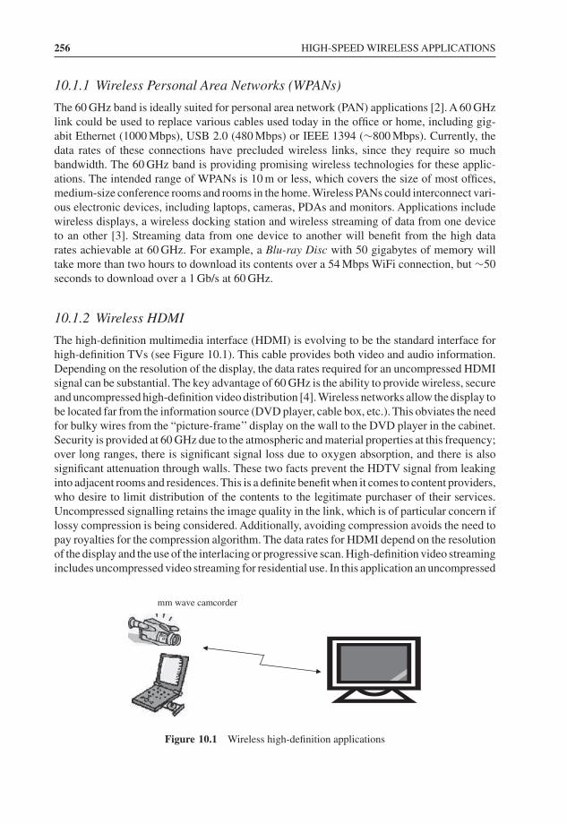
256 HIGH-SPEED WIRELESS APPLICATIONS
10.1.1 Wireless Personal Area Networks (WPANs)
The 60 GHz band is ideally suited for personal area network (PAN) applications [2]. A 60 GHzlink could be used to replace various cables used today in the office or home, including gig-abit Ethernet (1000 Mbps), USB 2.0 (480 Mbps) or IEEE 1394 (∼800 Mbps). Currently, thedata rates of these connections have precluded wireless links, since they require so muchbandwidth. The 60 GHz band is providing promising wireless technologies for these applic-ations. The intended range of WPANs is 10 m or less, which covers the size of most offices,medium-size conference rooms and rooms in the home. Wireless PANs could interconnect vari-ous electronic devices, including laptops, cameras, PDAs and monitors. Applications includewireless displays, a wireless docking station and wireless streaming of data from one deviceto an other [3]. Streaming data from one device to another will benefit from the high datarates achievable at 60 GHz. For example, a Blu-ray Disc with 50 gigabytes of memory willtake more than two hours to download its contents over a 54 Mbps WiFi connection, but ∼50seconds to download over a 1 Gb/s at 60 GHz.
10.1.2 Wireless HDMI
The high-definition multimedia interface (HDMI) is evolving to be the standard interface forhigh-definition TVs (see Figure 10.1). This cable provides both video and audio information.Depending on the resolution of the display, the data rates required for an uncompressed HDMIsignal can be substantial. The key advantage of 60 GHz is the ability to provide wireless, secureand uncompressed high-definition video distribution [4]. Wireless networks allow the display tobe located far from the information source (DVD player, cable box, etc.). This obviates the needfor bulky wires from the “picture-frame’’ display on the wall to the DVD player in the cabinet.Security is provided at 60 GHz due to the atmospheric and material properties at this frequency;over long ranges, there is significant signal loss due to oxygen absorption, and there is alsosignificant attenuation through walls. These two facts prevent the HDTV signal from leakinginto adjacent rooms and residences. This is a definite benefit when it comes to content providers,who desire to limit distribution of the contents to the legitimate purchaser of their services.Uncompressed signalling retains the image quality in the link, which is of particular concern iflossy compression is being considered. Additionally, avoiding compression avoids the need topay royalties for the compression algorithm. The data rates for HDMI depend on the resolutionof the display and the use of the interlacing or progressive scan. High-definition video streamingincludes uncompressed video streaming for residential use. In this application an uncompressed
mm wave camcorder
Figure 10.1 Wireless high-definition applications
V-BAND ANTENNA APPLICATIONS 257
video/audio stream is sent from a DVD player to an HDTV. A typical distance between themwould be 5 to 10 m with either a LOS or NLOS connection [5]. The high-definition streamscan also come from portable devices such as a laptop computer, personal data assistant (PDA)or portable media player (PMP), placed somewhere in the same room with an HDTV. In thissetting, the coverage range might be 3 to 5 m with either a LOS or NLOS connection. NLOSmay produce the best results because the direct propagation path may be temporarily blockedby human bodies or objects. Uncompressed video streaming can also be used for a laptop-to-projector connection in a conference room where people can share the same projector andeasily connect to the projector without switching cables, as has to happen in the case of cableconnection.
The WirelessHD 1.0 specification was launched in January 2008. It is architected andoptimised for wireless display connectivity, achieving in its first generation implementationhigh-speed rates from 2 to 5 Gb/s for the CE, PC and portable device segments. Its coretechnology projects theoretical data rates as high as 20 Gb/s, permitting it to scale to higherresolutions, colour depth and range. Coexisting with other wireless services, the WirelessHDplatform is designed to operate cooperatively with existing, wireline display technologies.
The recent availability of several new technologies makes it possible to achieve the multi-gigabit data rates required for uncompressed video streaming [6]. Such breakthroughs enablelow cost, better image quality and higher performance wireless A/V systems. The majorcharacteristics and key technologies include:
• High interoperability supported by major CE device manufacturers• Uncompressed HD video, audio and data transmission, scalable to future high-definition
A/V formats• High-speed wireless, multigigabit technology in the unlicensed 60 GHz band• Smart antenna technology to overcome line-of-sight constraints of 60 GHz• Secure communications• Device control for simple operation of consumer electronic products• Error protection, framing and timing control techniques for a quality consumer experience
10.1.3 Point-to-Point 60 GHz Links
Point-to-point links are used today for telecommunications backhauls [7]. They employ high-gain antennas to increase the range of the link. The 60 GHz band is being used in the marketplacetoday for such links, and the corresponding chips are implemented in III–V technologies.Silicon offers the best promise to reduce the cost of these systems, though the bulk of thesystem cost is still installation fees, requiring someone to install the equipment on top of apole. In Figure 10.2, ad hoc information distribution with a point-to-point network extensionmakes advertisement distribution or contents downloading services easy, and allows immediateconstruction, for example in an exhibition site.
10.1.4 Broadcasting a Video Signal Transmission System in aSports Stadium
Using the 60 GHz technology on an HDTV camera system, images and audio signals can betransferred from a video camera to a monitoring or recording facility. Such a system is used
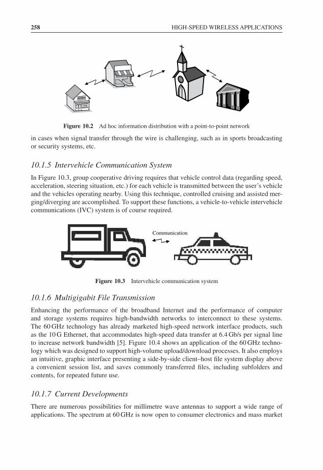
258 HIGH-SPEED WIRELESS APPLICATIONS
Figure 10.2 Ad hoc information distribution with a point-to-point network
in cases when signal transfer through the wire is challenging, such as in sports broadcastingor security systems, etc.
10.1.5 Intervehicle Communication System
In Figure 10.3, group cooperative driving requires that vehicle control data (regarding speed,acceleration, steering situation, etc.) for each vehicle is transmitted between the user’s vehicleand the vehicles operating nearby. Using this technique, controlled cruising and assisted mer-ging/diverging are accomplished. To support these functions, a vehicle-to-vehicle intervehiclecommunications (IVC) system is of course required.
Communication
Figure 10.3 Intervehicle communication system
10.1.6 Multigigabit File Transmission
Enhancing the performance of the broadband Internet and the performance of computerand storage systems requires high-bandwidth networks to interconnect to these systems.The 60 GHz technology has already marketed high-speed network interface products, suchas the 10 G Ethernet, that accommodates high-speed data transfer at 6.4 Gb/s per signal lineto increase network bandwidth [5]. Figure 10.4 shows an application of the 60 GHz techno-logy which was designed to support high-volume upload/download processes. It also employsan intuitive, graphic interface presenting a side-by-side client–host file system display abovea convenient session list, and saves commonly transferred files, including subfolders andcontents, for repeated future use.
10.1.7 Current Developments
There are numerous possibilities for millimetre wave antennas to support a wide range ofapplications. The spectrum at 60 GHz is now open to consumer electronics and mass market
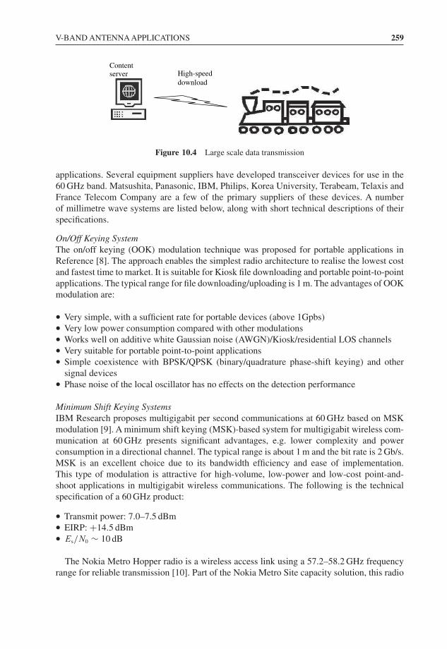
V-BAND ANTENNA APPLICATIONS 259
High-speeddownload
Contentserver
Figure 10.4 Large scale data transmission
applications. Several equipment suppliers have developed transceiver devices for use in the60 GHz band. Matsushita, Panasonic, IBM, Philips, Korea University, Terabeam, Telaxis andFrance Telecom Company are a few of the primary suppliers of these devices. A numberof millimetre wave systems are listed below, along with short technical descriptions of theirspecifications.
On/Off Keying SystemThe on/off keying (OOK) modulation technique was proposed for portable applications inReference [8]. The approach enables the simplest radio architecture to realise the lowest costand fastest time to market. It is suitable for Kiosk file downloading and portable point-to-pointapplications. The typical range for file downloading/uploading is 1 m. The advantages of OOKmodulation are:
• Very simple, with a sufficient rate for portable devices (above 1Gpbs)• Very low power consumption compared with other modulations• Works well on additive white Gaussian noise (AWGN)/Kiosk/residential LOS channels• Very suitable for portable point-to-point applications• Simple coexistence with BPSK/QPSK (binary/quadrature phase-shift keying) and other
signal devices• Phase noise of the local oscillator has no effects on the detection performance
Minimum Shift Keying SystemsIBM Research proposes multigigabit per second communications at 60 GHz based on MSKmodulation [9]. A minimum shift keying (MSK)-based system for multigigabit wireless com-munication at 60 GHz presents significant advantages, e.g. lower complexity and powerconsumption in a directional channel. The typical range is about 1 m and the bit rate is 2 Gb/s.MSK is an excellent choice due to its bandwidth efficiency and ease of implementation.This type of modulation is attractive for high-volume, low-power and low-cost point-and-shoot applications in multigigabit wireless communications. The following is the technicalspecification of a 60 GHz product:
• Transmit power: 7.0–7.5 dBm• EIRP: +14.5 dBm• Es/N0 ∼ 10 dB
The Nokia Metro Hopper radio is a wireless access link using a 57.2–58.2 GHz frequencyrange for reliable transmission [10]. Part of the Nokia Metro Site capacity solution, this radio
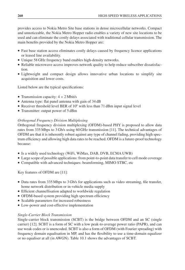
260 HIGH-SPEED WIRELESS APPLICATIONS
provides access to Nokia Metro Site base stations in dense microcellular networks. Compactand unnoticeable, the Nokia Metro Hopper radio enables a variety of new site locations to beused and can eliminate the costly delays associated with traditional cellular transmission. Themain benefits provided by the Nokia Metro Hopper are:
• Fast base station access eliminates costly delays caused by frequency licence applicationsor leased line availability.
• Unique 58 GHz frequency band enables high-density networks.• Reliable microwave access improves network quality to help reduce subscriber dissatisfac-
tion.• Lightweight and compact design allows innovative urban locations to simplify site
acquisition and lower costs.
Listed below are the typical specifications:
• Transmission capacity: 4 × 2 Mbit/s• Antenna type: flat panel antenna with gain of 34 dB• Receiver threshold level BER of 106 with less than 71 dBm input signal level• Transmitter: output power of 5 dBm
Orthogonal Frequency Division MultiplexingOrthogonal frequency division multiplexing (OFDM)-based PHY is proposed to allow datarates from 335 Mbps to 3 Gb/s using 60 GHz transmission [11]. The technical advantages ofOFDM are that it is inherently robust against any type of channel fading, providing high spec-trum efficiency and allowing high data rates to be reached. OFDM is a future-proof technologybecause:
• Is a widely used technology (WiFi, WiMax, DAB, DVB, ECMA UWB)• Large scope of possible applications: from point-to-point data transfer to cell mode coverage• Compatible with advanced techniques: beamforming, MIMO STBC, etc
Key features of OFDM are [11]:
• Data rates from 335 Mbps to 3 Gb/s for applications such as video streaming, file transfer,home network distribution or in-vehicle media supply
• Efficient channellisation adapted to worldwide regulation• OFDM-based system providing high spectrum efficiency• Scalable parameters for increased robustness• Low-power and cost-effective implementation
Single-Carrier Block TransmissionSingle-carrier block transmission (SCBT) is the bridge between OFDM and an SC (singlecarrier) [12]. SCBT is a form of SC with a low peak-to-average power ratio (PAPR), and canuse weak codes or is unencoded. SCBT is also a form of OFDM (with Fourier spreading) withfrequency domain equalisation in MP, and has the flexibility to use a time-domain equalizeror no equaliser at all (in AWGN). Table 10.1 shows the advantages of SCBT.
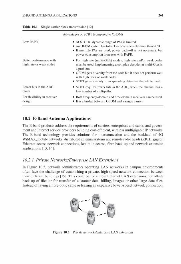
E-BAND ANTENNA APPLICATIONS 261
Table 10.1 Single-carrier block transmission [12]
Advantages of SCBT (compared to OFDM)
Low PAPR • At 60 GHz, dynamic range of PAs is limited.• An OFDM system has to back-off considerably more than SCBT.• If multiple PAs are used, power back-off is not necessary, but
power consumption increases with PAPR.
Better performance withhigh rate or weak codes
• For high rate (multi-Gb/s) modes, high rate and/or weak codesmust be used. Implementing a complex decoder at multi-Gb/s isa problem.
• OFDM gets diversity from the code but it does not perform wellwith high rates or weak codes.
• SCBT gets diversity from spreading data over the whole band.
Fewer bits in the ADCblock
• SCBT requires fewer bits in the ADC, when the channel has alow number of multipaths.
For flexibility in receiverdesign
• Both frequency-domain and time-domain receivers can be used.• It is a bridge between OFDM and a single carrier.
10.2 E-Band Antenna Applications
The E-band products address the requirements of carriers, enterprises and cable, and govern-ment and Internet service providers building cost-efficient, wireless multigigabit IP networks.The E-band technology provides solutions for interconnection and the backhaul of 4G,WiMAX, mobile networks, distributed antenna systems and remote radio heads (RRH), gigabitEthernet access network connections, last mile access, fibre back-up and network extensionapplications [13, 14].
10.2.1 Private Networks/Enterprise LAN Extensions
In Figure 10.5, network administrators operating LAN networks in campus environmentsoften face the challenge of establishing a private, high-speed network connection betweentheir different buildings [15]. This could be for simple Ethernet LAN extensions, for offsiteback-up of files or for transfer of customer data, billing, images or other large data files.Instead of laying a fibre-optic cable or leasing an expensive lower-speed network connection,
Figure 10.5 Private networks/enterprise LAN extensions
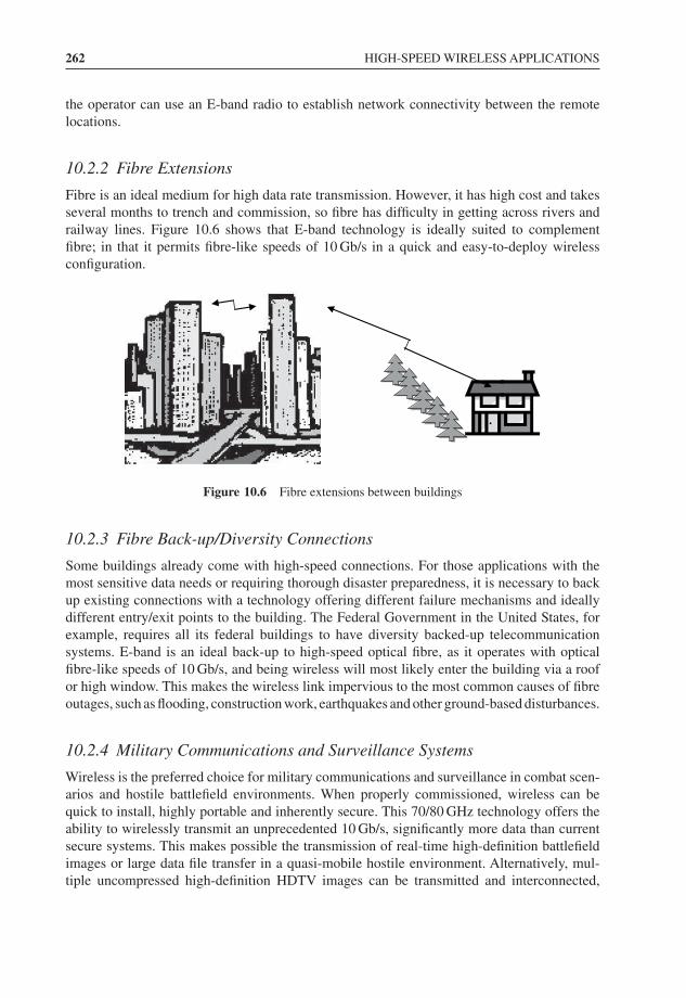
262 HIGH-SPEED WIRELESS APPLICATIONS
the operator can use an E-band radio to establish network connectivity between the remotelocations.
10.2.2 Fibre Extensions
Fibre is an ideal medium for high data rate transmission. However, it has high cost and takesseveral months to trench and commission, so fibre has difficulty in getting across rivers andrailway lines. Figure 10.6 shows that E-band technology is ideally suited to complementfibre; in that it permits fibre-like speeds of 10 Gb/s in a quick and easy-to-deploy wirelessconfiguration.
Figure 10.6 Fibre extensions between buildings
10.2.3 Fibre Back-up/Diversity Connections
Some buildings already come with high-speed connections. For those applications with themost sensitive data needs or requiring thorough disaster preparedness, it is necessary to backup existing connections with a technology offering different failure mechanisms and ideallydifferent entry/exit points to the building. The Federal Government in the United States, forexample, requires all its federal buildings to have diversity backed-up telecommunicationsystems. E-band is an ideal back-up to high-speed optical fibre, as it operates with opticalfibre-like speeds of 10 Gb/s, and being wireless will most likely enter the building via a roofor high window. This makes the wireless link impervious to the most common causes of fibreoutages, such as flooding, construction work, earthquakes and other ground-based disturbances.
10.2.4 Military Communications and Surveillance Systems
Wireless is the preferred choice for military communications and surveillance in combat scen-arios and hostile battlefield environments. When properly commissioned, wireless can bequick to install, highly portable and inherently secure. This 70/80 GHz technology offers theability to wirelessly transmit an unprecedented 10 Gb/s, significantly more data than currentsecure systems. This makes possible the transmission of real-time high-definition battlefieldimages or large data file transfer in a quasi-mobile hostile environment. Alternatively, mul-tiple uncompressed high-definition HDTV images can be transmitted and interconnected,
E-BAND ANTENNA APPLICATIONS 263
allowing real-time monitoring of multiple security images or viewing of secure locationsat the same time.
10.2.5 Secure Applications
E-band systems offer huge military and government potential. Very high data rates, portab-ility and ease of deployment make E-band communications ideal for homeland defence andother security purposes. Rapidly deployable, high-definition video links can be used for highdata rate for event security such as facial mapping for recognition [16]. Another is high datarate battlefield data distribution from satellites. E-band systems excel in military applicationssince the millimetre wave properties allow the radio to be classified as low-probability-of-detect/low-probability-of-intercept (LPD/LPI). For any point-to-point technology, antennasgenerally have to be placed on high towers or masts, so a clear line-of-sight can be achieved.By necessity, this means that few buildings or possible interception points can be close tothe radio path. However, the ether between any two antennas is never secure, and a determ-ined hacker with a basic understanding of the particular radio system architecture will beable to intercept part of the broad transmission radio signal. E-band systems, however, have afrequency much higher than conventional wireless systems, resulting in antennas that have amuch greater focusing ability.A typical application with a 0.6 m dish antenna has a very narrow0.3◦ beamwidth, meaning that transmitted signals propagate as highly focused and directionalpencil beams from the antenna. Transmitted signals do not form broad diverging beams thatilluminate large areas as at lower frequencies. For the 0.6 m E-band scenario, the beam willspread in a cone shape over 30◦. Thus, an E-band product’s narrow pencil beams are inherentlymuch harder to locate and are far more difficult to intercept.
Table 10.2 shows the comparison between all the high data rate transmission technologies.The 70/80 GHz technology gives the best performance compared with other technologies.
Table 10.2 Comparison of the performance of all the available high data rate transmission technolo-gies [17]
70/80 GHz 60 GHz radio Free space optics Buried fibre
Data rates 1 Gb/s 1 Gb/s 1 Gb/s Virtuallyunlimited
Typical link distances (99.999 %availability)
1.6 km 366 m 183 m Virtuallyunlimited
Relative product complexity Low Low High Low
Relative cost of installation andownership
Low Low Low High
Installation time Hours Hours Hours Months
Regulatory protection Yes No No Yes
In conclusion, E-band wireless communications is a new technology that allows gigabit persecond (Gb/s) data rates to be transmitted with very high weather tolerances over distances ofa mile or more. Characterised as LPD/LPI, it is a perfect technology to satisfy hostile territory
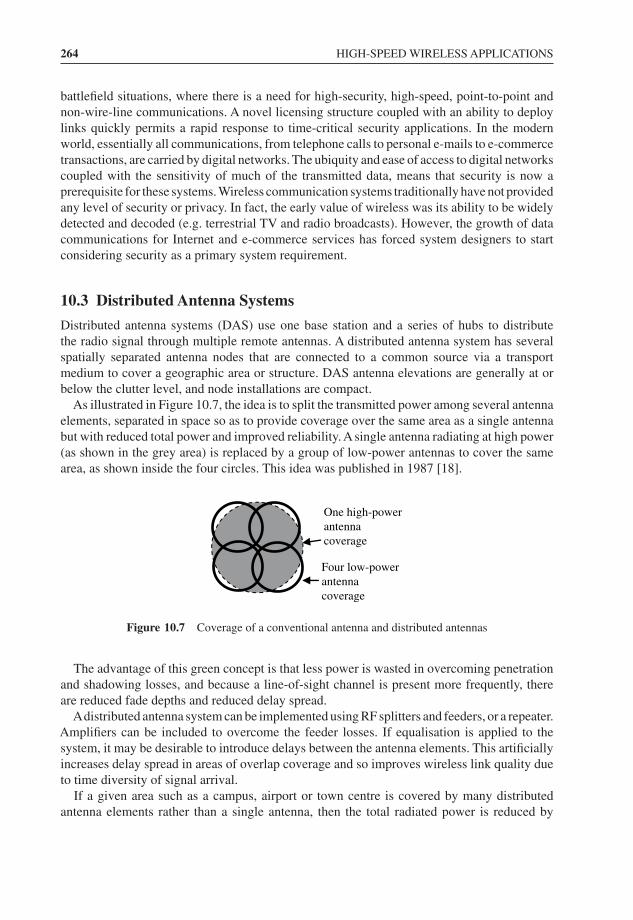
264 HIGH-SPEED WIRELESS APPLICATIONS
battlefield situations, where there is a need for high-security, high-speed, point-to-point andnon-wire-line communications. A novel licensing structure coupled with an ability to deploylinks quickly permits a rapid response to time-critical security applications. In the modernworld, essentially all communications, from telephone calls to personal e-mails to e-commercetransactions, are carried by digital networks. The ubiquity and ease of access to digital networkscoupled with the sensitivity of much of the transmitted data, means that security is now aprerequisite for these systems.Wireless communication systems traditionally have not providedany level of security or privacy. In fact, the early value of wireless was its ability to be widelydetected and decoded (e.g. terrestrial TV and radio broadcasts). However, the growth of datacommunications for Internet and e-commerce services has forced system designers to startconsidering security as a primary system requirement.
10.3 Distributed Antenna Systems
Distributed antenna systems (DAS) use one base station and a series of hubs to distributethe radio signal through multiple remote antennas. A distributed antenna system has severalspatially separated antenna nodes that are connected to a common source via a transportmedium to cover a geographic area or structure. DAS antenna elevations are generally at orbelow the clutter level, and node installations are compact.
As illustrated in Figure 10.7, the idea is to split the transmitted power among several antennaelements, separated in space so as to provide coverage over the same area as a single antennabut with reduced total power and improved reliability. A single antenna radiating at high power(as shown in the grey area) is replaced by a group of low-power antennas to cover the samearea, as shown inside the four circles. This idea was published in 1987 [18].
One high-powerantennacoverage
Four low-powerantennacoverage
Figure 10.7 Coverage of a conventional antenna and distributed antennas
The advantage of this green concept is that less power is wasted in overcoming penetrationand shadowing losses, and because a line-of-sight channel is present more frequently, thereare reduced fade depths and reduced delay spread.
Adistributed antenna system can be implemented using RF splitters and feeders, or a repeater.Amplifiers can be included to overcome the feeder losses. If equalisation is applied to thesystem, it may be desirable to introduce delays between the antenna elements. This artificiallyincreases delay spread in areas of overlap coverage and so improves wireless link quality dueto time diversity of signal arrival.
If a given area such as a campus, airport or town centre is covered by many distributedantenna elements rather than a single antenna, then the total radiated power is reduced by
DISTRIBUTED ANTENNA SYSTEMS 265
approximately a factor of N 1−n/2 and the power per antenna is reduced by a factor of Nn/2,where a simple power law path loss model with a path loss exponent n is assumed. As analternative, the total area covered could be extended for a given limit of effective radiatedpower, which may be important to ensure compliance with safety limits on radiation exposureof the human body.
Some distributed antenna systems use large coaxial cables to distribute the signal through avenue: typically, coaxial cable is used in the building risers, with coaxial cable diverging fromthis backbone, running horizontally and feeding antennas at the run’s endpoint. These systemsare considered to be passive because they do not use managed electronics in the distributionnetwork.
A passive distributed antenna system is expensive to install (large coaxial cable requiresspecial installation labour and installation time can be lengthy). In addition, the signal ina passive system attenuates over longer cable runs, leading to inconsistent signal strength.This makes system design/engineering difficult as each antenna’s coverage area will vary,depending on the length of coax to which it is attached. This leads to another issue: with apassive distributed antenna system, the whole system may require re-engineering if additionalcapacity is added or if additional coverage areas are required. Finally, passive systems aredifficult or impossible to manage: if an antenna malfunctions, only user complaints will alertthe operator. Typically, passive distributed antenna systems are deployed in smaller facilitieswhere the length of a coaxial cable run is less of an issue.
Passive distributed antenna systems, like most technologies, have their problems. The threeprimary disadvantages to distributed antenna system solutions are cost, carrier costs and a lackof standards:
1. Costs for in building coverage can exceed a dollar or more per square foot; this adds upquickly in a large building. Costs to supplement outdoor coverage must be determinedindividually, since there are many variables. One way to economise in a distributed antennasystem (DAS) installation is to equip the building during the building process, which meansa network design needs to be developed in advance and the necessary trunking put inplace for the routing of DAS cables both horizontally and vertically, as is implementedfor plumbing, electricity and Ethernet. This early design in conjunction with the architectshould also include determining where the head end should be placed and selecting cableroutes to the roof for antennas.
2. Cooperative wireless carriers. In order to extend or enhance wireless service in a domain,the owner needs active support from its service providers. Carriers are responsible forcompliance with national regulations such as avoiding interference between systems, so iftheir signals are to be re-broadcast by a third party, the carriers must ensure such compli-ance. Frequently however, carriers are not interested in getting involved in implementationunless they anticipate a significant increase in the traffic and revenue. They also may bereluctant if they believe competition will be too great in a multiple-provider situation.If good coverage is required from multiple providers, consideration needs to be givento a “neutral host’’ type of system. Typically, those that implement these systems haveinfluence to bring multiple service providers together. The role may also include nego-tiating revenue-sharing agreements with these carriers to minimise overall maintenancecosts.

266 HIGH-SPEED WIRELESS APPLICATIONS
3. Standards. Here, neither the IEEE nor the ITU has developed a standard for distributedantenna systems. This unfortunate situation is similar to that of networking, before Ethernetbecame the accepted standard: with many competing proprietary technologies. It is thereforeessential that those who select the operating system understand the pros and cons of thevarious manufacturers’products and the associated methodologies of the designs. Unbiasedthird parties (such as independent consultants) can assist by helping assess the wireless needsof the client, and then to develop budgetary estimates to give an idea of the range of costslikely to be incurred.
Active distributed antenna systems utilise active hubs, fibre optics, active radio access units(RAUs) and antennas to distribute the signal. These systems sustain high signal strength atevery antenna location, independent of the distance from the central transceiver. Some activedistributed antenna systems extend over several miles, and many systems support optimumsignal strength throughout the interiors of buildings and other facilities measuring millions ofsquare metres. In addition, active distributed antenna systems offer end-to-end monitoring andmanagement down to the individual antenna, ensuring that outages will quickly be reportedand repaired.
Active DAS systems address all of the problems that are met when deploying pico cellsystems:
1. Costs. Active distributed antenna systems are much smaller, cost less and are less intrusivethan pico cells aesthetically. In addition, active distributed antenna systems use standardcabling to connect hubs to RAUs and remote antennas, so this expedites installation andreduces costs when compared to passive distributed antenna systems.
2. Terminal density. With an active DAS, there is no limit to the number of antennas. Eachantenna is an extension of the central radio source (all antennas in the system broadcast allchannels from the radio source), so there is no need to design the system at each individualantenna level to meet the needs in hot spot areas.
3. Interference. Because the system operates off of a single radio source, there is no problemwith interference among antennas.
4. Longer term savings. Distributed antenna systems use low cost RAUs and antennas tosupport high-capacity areas, users need to invest less capital in expensive access points thatmay be infrequently used.
5. Multi Carrier Capability. Unlike pico cells, both active and passive distributed antennasystems can support multiple carriers in a single-antenna system, making it a relativelyeasy matter to upgrade centralised or hub electronics so they can support new carriers orservices.
6. Capacity. In an active distributed antenna system, capacity issues are addressed at the centralbase station. If additional capacity is required, the number of radios at the central source issimply increased. This is in contrast to pico cells, where it may be necessary to add moreradio resources at every pico-cell to support extra users, which is costly.
7. Interfaces. Major communications carriers throughout the world have installed large num-bers of distributed antenna systems, and therefore the interfaces to base stations and thenetwork are well known. Active distributed antenna systems are the in-building systemschosen to provide coverage inside most major cellular company headquarters.
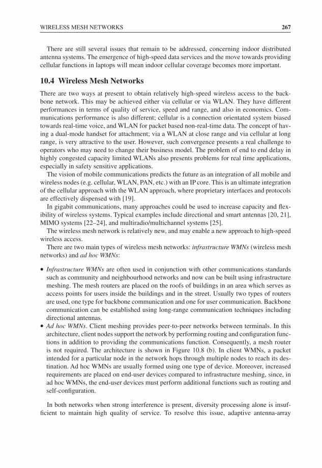
WIRELESS MESH NETWORKS 267
There are still several issues that remain to be addressed, concerning indoor distributedantenna systems. The emergence of high-speed data services and the move towards providingcellular functions in laptops will mean indoor cellular coverage becomes more important.
10.4 Wireless Mesh Networks
There are two ways at present to obtain relatively high-speed wireless access to the back-bone network. This may be achieved either via cellular or via WLAN. They have differentperformances in terms of quality of service, speed and range, and also in economics. Com-munications performance is also different; cellular is a connection orientated system biasedtowards real-time voice, and WLAN for packet based non-real-time data. The concept of hav-ing a dual-mode handset for attachment; via a WLAN at close range and via cellular at longrange, is very attractive to the user. However, such convergence presents a real challenge tooperators who may need to change their business model. The problem of end to end delay inhighly congested capacity limited WLANs also presents problems for real time applications,especially in safety sensitive applications.
The vision of mobile communications predicts the future as an integration of all mobile andwireless nodes (e.g. cellular, WLAN, PAN, etc.) with an IP core. This is an ultimate integrationof the cellular approach with the WLAN approach, where proprietary interfaces and protocolsare effectively dispensed with [19].
In gigabit communications, many approaches could be used to increase capacity and flex-ibility of wireless systems. Typical examples include directional and smart antennas [20, 21],MIMO systems [22–24], and multiradio/multichannel systems [25].
The wireless mesh network is relatively new, and may enable a new approach to high-speedwireless access.
There are two main types of wireless mesh networks: infrastructure WMNs (wireless meshnetworks) and ad hoc WMNs:
• Infrastructure WMNs are often used in conjunction with other communications standardssuch as community and neighbourhood networks and now can be built using infrastructuremeshing. The mesh routers are placed on the roofs of buildings in an area which serves asaccess points for users inside the buildings and in the street. Usually two types of routersare used, one type for backbone communication and one for user communication. Backbonecommunication can be established using long-range communication techniques includingdirectional antennas.
• Ad hoc WMNs. Client meshing provides peer-to-peer networks between terminals. In thisarchitecture, client nodes support the network by performing routing and configuration func-tions in addition to providing the communications function. Consequently, a mesh routeris not required. The architecture is shown in Figure 10.8 (b). In client WMNs, a packetintended for a particular node in the network hops through multiple nodes to reach its des-tination. Ad hoc WMNs are usually formed using one type of device. Moreover, increasedrequirements are placed on end-user devices compared to infrastructure meshing, since, inad hoc WMNs, the end-user devices must perform additional functions such as routing andself-configuration.
In both networks when strong interference is present, diversity processing alone is insuf-ficient to maintain high quality of service. To resolve this issue, adaptive antenna-array
268 HIGH-SPEED WIRELESS APPLICATIONS
Figure 10.8 (a) Point-to-multipoint network and (b) fixed mesh network
processing is used to shape the antenna beam in order to enhance the desired signals whilenulling the interfering signals. Antenna diversity and smart antenna techniques are alsoapplicable to WMNs and other ad hoc networks.
Examples of analysing smart antenna systems for mobile ad hoc networks are reported inReferences [20] and [26]. Due to complexity and cost, a fully adaptive smart antenna systemis only used in base stations of cellular networks. Ongoing research and further developmentis still needed to implement fully adaptive smart antenna systems in a mobile terminal. ForWMNs, achieving low cost is a challenge. To this end directional antennas have been activelyresearched in the area of ad hoc networks.
A mechanically or electronically steerable or switched directional antenna system can beconfigured to track a terminal signal. By using directional transmission, interference betweennetwork nodes can be mitigated and, thus, network capacity can be improved [21, 27]. Direc-tional antennas can also improve power efficiency [28]. However, directional antennas bringproblems for the MAC protocol design [29, 30].
Directional-antenna-based MAC schemes can eliminate exposed nodes if the antenna beamis assumed to be perfect. However, due to the directional transmission, more hidden nodes aregenerated. Therefore, new solutions must be developed to reduce the number of hidden nodes.Ultimately, MAC protocols based on directional antennas face other challenges such as cost,system complexity and the practicality of fast steerable directional antennas.
Most systems support variable bit rate access for a diverse range of mobile devices. Thisdemands a provision of service that is well supported by TCP/IP. The core network is thenused to connect the users to the Internet via Internet service providers (ISPs).
Content providers are closely associated with ISPs in some business models. The networkclasses linked into the core are:
• Personal area network (PAN). This may, for example, use Bluetooth which may support amesh like architecture. Speed is currently under 1Mb/s (although 100 Mb/s is predicted) andthe range is short, e.g. 10 m. No infrastructure is needed, except for an access point to abackbone.
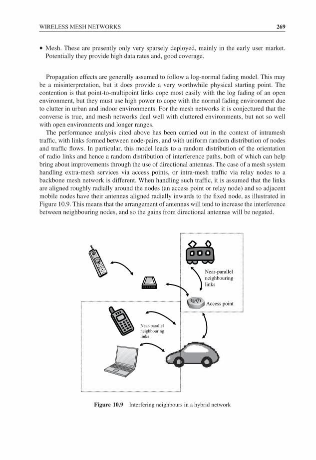
WIRELESS MESH NETWORKS 269
• Mesh. These are presently only very sparsely deployed, mainly in the early user market.Potentially they provide high data rates and, good coverage.
Propagation effects are generally assumed to follow a log-normal fading model. This maybe a misinterpretation, but it does provide a very worthwhile physical starting point. Thecontention is that point-to-multipoint links cope most easily with the log fading of an openenvironment, but they must use high power to cope with the normal fading environment dueto clutter in urban and indoor environments. For the mesh networks it is conjectured that theconverse is true, and mesh networks deal well with cluttered environments, but not so wellwith open environments and longer ranges.
The performance analysis cited above has been carried out in the context of intrameshtraffic, with links formed between node-pairs, and with uniform random distribution of nodesand traffic flows. In particular, this model leads to a random distribution of the orientationof radio links and hence a random distribution of interference paths, both of which can helpbring about improvements through the use of directional antennas. The case of a mesh systemhandling extra-mesh services via access points, or intra-mesh traffic via relay nodes to abackbone mesh network is different. When handling such traffic, it is assumed that the linksare aligned roughly radially around the nodes (an access point or relay node) and so adjacentmobile nodes have their antennas aligned radially inwards to the fixed node, as illustrated inFigure 10.9. This means that the arrangement of antennas will tend to increase the interferencebetween neighbouring nodes, and so the gains from directional antennas will be negated.
Near-parallelneighbouringlinks
Near-parallelneighbouringlinks
Access point
Figure 10.9 Interfering neighbours in a hybrid network
270 HIGH-SPEED WIRELESS APPLICATIONS
In order to improve the performance of a wireless radio and its control by higher- layerprotocols many techniques have been employed. These include more advanced radio tech-nologies, such as reconfigurable radios, frequency agile/cognitive radios [31–33] and evensoftware radios [34]. Many of these radio technologies are still in their early stages of develop-ment, they are expected to be the platform for future wireless networks owing to their abilityto dynamically control the radio links.
There are two problems associated with the physical layer. Firstly, it is necessary to furtherimprove the transmission rate and the performance of physical layer techniques. New widebandtransmission schemes in addition to OFDM or UWB are needed in order to achieve a highertransmission rate in larger area networks. Multiple-antenna systems have been studied for sometime. However, their complexity and cost are still too high to be widely accepted for WMNs.A low-cost directional antenna implementation is reported in Reference [35]. Frequency-agiletechniques are also at an early stage. Many issues need to be resolved before they can beaccepted for commercial use [33].
Secondly, to fully utilise the advanced features provided by the physical layer, higher levelprotocols, especially MAC protocols, need to be carefully designed. Otherwise, the advantagesbrought by these physical layer schemes could be compromised. For directional and smartantennas, many MAC protocols have been proposed for ad hoc networks [29, 30]. A MACprotocol for MIMO systems is studied in Reference [23].
Therefore advanced wireless radio technologies all require a revolutionary design in antenna-related technology. For example, when directional antennas are applied to IEEE 802.15.3cnetworks, a routing protocol needs to take into account the selection of directional antennasectors. Directional antennas can reduce exposed nodes, but they also generate more hiddennodes. Thus, MAC protocols ought to be redesigned to resolve this issue. The same principleapplies to MIMO systems [23]. Therefore, much research work is needed to develop millimetrewave antennas for these future applications.
References[1] Bridge Wave Communications, ‘Gigabit Wireless Applications Using 60 GHz Radios’, 2007.[2] Abbie Mathew, ‘Local Area Networking Using Millimetre Waves’, NewLANs, Inc., USA, 2005.[3] Chinh H. Doan, Sohrab Emami, Ali M. Niknejad and Robert W. Brodersen, ‘Design of CMOS for 60 GHz
Applications’, University of California, Berkeley Wireless Research Center, Berkeley, 2005.[4] S. Li, ‘Designing for High Definition Video with Multi-Gigabit Wireless Technologies’, Sibeam White Paper,
November 2005.[5] Eino Kivisaari, ‘60 GHZ MMW Applications’, Helsinki University of Technology, Telecommunications
Software and Multimedia Laboratory, Finland, 2003.[6] Nan Guo, Robert C. Qiu, Shaomin S.Mo and Kazuaki Takahashi, ‘60-GHz Millimeter-Wave Radio: Principle,
Technology, and New Results’, EURASIP Journal on Wireless Communications and Networking, 2007, ArticleID 68253, DOI:10.1155/2007/68253.
[7] Dong-Young Kim, ‘60 GHz SoP Design Using LTCC’, Microwave Devices Team, ETRI, 2006.[8] ‘Panasonic PHY and MAC Proposal to IEEE802.15 TG3c CFP’, IEEE 802.15 Working Group for Wireless
Personal Area Network (WPAN), May 2007.[9] ‘Summary of Link Experiments and MSK-Based Preliminary Proposal for Multi-GB/s Communications at
60 GHz’, IEEE 802.15 Working Group for Wireless Personal Area Network (WPAN), March 2007.[10] Nokia_MetrohopperTM Radio, Nokia leaflet.[11] France Telecom, ‘Proposition of a High Data Rate Wireless System in the 60 GHz Range, Providing Data Rates
Ranging from 335 Mbps to 3 Gb/s’, IEEE 802.15 Working Group for Wireless Personal Area Network (WPAN),7 May 2007.

REFERENCES 271
[12] ‘SCBT Based 60 GHz PHYProposa’, IEEE 802.15 Working Group for Wireless PersonalArea Network (WPAN),May 2007.
[13] Jonathan Wells, ‘Multi-Gigabit Wireless Technology at 70 GHz, 80 GHz and 90 GHz’, Gigabeam Corporation,2006.
[14] John Cox, ‘E-Band Radio for High-Capacity Links’, NetworkWorld.com, 17 February 2006.[15] ‘Millimetre Wave Communication System’, Lumera Data Sheet, http://www. lumera.com/home.php[16] Jonathan Wells, ‘New Multi-Gigabit Wireless Systems Satisfy High-Security Rapid Response Applications’,
Military Embedded Systems, Spring 2006.[17] Jonathan Wells, White Paper on ‘WiMAX Backhaul at 70/80 GHz’, Gigabeam Corporation, USA, 2006.[18] A. A. M. Saleh and R. A. Valenzuela, ‘A Statistical Model for Indoor Multipath Propagation, IEEE Journal of
Selected Areas in Communications, SAC-5, February 1987, 128.[19] Ahmad Atefi, ‘Final Report – Study of Efficient Mobile Mesh’, OFCOM Document AYR005, January 2006.[20] R. Ramanathan, ‘On the Performance of Ad Hoc Networks with Beamforming Antennas’, ACM International
Symposium on ‘Mobile Ad Hoc Networking and Computing (MOBIHOC)’, October 2001, pp. 95–105.[21] A. Spyropoulos and C. S. Raghavendra, Asymptotic Capacity Bounds for Ad Hoc Networks Revisited: The
Directional and Smart Antenna Cases’, IEEE Global Telecommunications Conference (GLOBECOM), 2003,pp. 1216–1220.
[22] W. Xiang, T. Pratt and X. Wang, ‘A Software Radio Testbed for Two-Transmitter Two-Receiver Space TimeCoding Wireless LAN’, IEEE Communications Magazine, 42(6), 2004, S20–S28.
[23] K. Sundaresan, R. Sivakumar, M. A. Ingram and T.-Y. Chang, ‘A Fair Medium Access Control Protocol forAd Hoc Networks with MIMO Links’, IEEE Annual Conference on Computer Communications (INFOCOM),2004, pp. 2559–2570.
[24] IEEE 802.11 Standard Group Website, <http://www.ieee802.org/11/>[25] J. So and N. Vaidya, ‘Multi-channel MAC for Ad Hoc Networks: Handling Multi-channel Hidden Terminals
Using a Single Transceiver’, ACM International Symposium on ‘Mobile Ad Hoc Networking and Computing(MOBIHOC)’, May 2004, pp. 222–233.
[26] S. Bellofiore, J. Foutz, R. Govindaradjula, I. Bahceci, C.A. Balanis,A. S. Spanias, J. M. Capone and T. M. Duman,‘Smart Antenna System Analysis, Integration and Performance for Mobile Ad Hoc Networks (MANETs)’, IEEETransactions on Antennas and Propagation, 50(5), 2002, 571–581.
[27] R. Ramanathan, J. Redi, C. Santivanez, D. Wiggins and S. Polit, ‘Ad Hoc Networking with Directional Antennas:A Complete System Solution’, IEEE Wireless Communications and Networking Conference (WCNC), 2004,pp. 375–380.
[28] A. Spyropoulos and C. S. Raghavendra, ‘Energy Efficient Communications in Ad Hoc Networks UsingDirectionalAntenna’, IEEEAnnual Conference on Computer Communications (INFOCOM), 2002, pp. 220–228.
[29] T.-S. Yum and K.-W. Hung, ‘Design Algorithms for Multihop Packet Radio Networks with Multiple DirectionalAntenna Stations’, IEEE Transactions on Communications, 41(11), 1992, 1716–1724.
[30] A. Nasipuri, S. Ye and R.E. Hiromoto, ‘A MAC Protocol for Mobile Ad Hoc Networks Using DirectionalAntennas’, IEEE Wireless Communications and Networking Conference (WCNC), 2000, pp. 1214–1219.
[31] Engim Inc., ‘Multiple Channel 802.11 Chipset’, Available from <http://www. engim.com/products_en3000.html>
[32] M. McHenry, ‘Frequency Agile Spectrum Access Technologies’, FCC Workshop on Cognitive Radios, May2003.
[33] B. Lane, ‘Cognitive Radio Technologies in the Commercial Arena’, FCC Workshop on Cognitive Radios, May2003.
[34] J. Mitola III, ‘Software Radio Architecture: Object-Oriented Approaches to Wireless System Engineering’, WileyInter-Science, New York, 2000.
[35] J. Kajiya, ‘Commodity Software Steerable Antennas for Mesh Networks’, Microsoft Mesh Networking Summit,June 2004.


Index
A/V network 2Ad hoc WMNs 267Adaptive beamforming 200, 212, 214Amplitude weight 176Analogue-to-digital conversion 215Angle-diversity 162, 172Antenna
dielectric 115–44horn 91–112lens 145–70material 227–54multiple antenna 171–94parameters 37–60planar 61–90smart 197–224
Aperture stacked patch 70Aperture-coupling 121Array
brick 183factor 159, 177, 178
Asymmetrical effect 135Atmospheric absorption 14, 15AWGN 16, 17, 30Axial ratio 43, 51–5, 57
Babinet’s principle 151Beam
steering 211–12, 216–18switching 29, 110–11
Bessel functions 92Binomial array 176Bit error rate 30, 200Blass matrix 209Blu-ray Disc 256Boresight 104Bow-tie antenna 76Butler matrix 163, 201, 209, 210
CB-CPW line 236CB-FGC line 235Channel capacity 190, 196, 212–13Chebyshev polynomial 177Circular waveguide modes 93Circular polarisation 28, 37CMOS 217–18, 228, 238–41Co-channel interference 172Coefficient of thermal expansion 234, 236–7Collating 229Complementary conducting strip 241Complementary dipole 72Converging lens 145Convex lens 145Cooperative wireless carriers 265Co-phased array 136Coplanar waveguide 68–70, 77, 236Corporate feeding network 200Coupling effect 109, 127, 128, 191Cross polarisation 43, 51, 52, 75–6, 135Crosshatched ground planes 231Cut-off frequency 65, 91–3
Degree of freedom 80, 163–4Dielectric
constant 65loss 66, 117membrane 100–1resonator antenna 115–21sectoral horn 111–12
Diffraction 44, 80, 109Digital
beamforming 36, 202, 203, 211wavenumber 177
Digital-to-analogue conversion 26Dipole 40, 41, 43, 48Direct conversion 24–5
Millimetre Wave Antennas for Gigabit Wireless Communications Kao-Cheng Huang and David J. Edwardsc© 2008 John Wiley & Sons, Ltd

274 INDEX
Direction of arrival 198, 204, 224Discontinuity radiation 122Discrete lens array 161, 163Dispersion 5, 92, 151Distortion 92Distributed antenna systems 264Dolph–Chebyshev array 177Doppler shift 15Dual rod 127
ECMA 10, 260Effective wavelength 149Efficiency 39, 65, 66EIRP 8, 15, 31, 219Electromagnetic bandgaps 40Ellipsoidal lens 154, 157, 159Embedded resistors 86Error protection 257European Radio-communications Committee 7Extended hemispherical lens 151
Fabry–Perot cavity 40–2Fast waves 184FCC 6, 8, 9, 15FDA 6Feeding methods 68, 69Fermat’s principle 146Fibre extensions 262Field effect transistors 238Filter lens array 207Fine-line printing 85Finite difference time-domain 122, 142First-order rays 155Five-port radio 25Flip chip 85Focal arc 162–3, 207Focal point 146Folded reflect antenna 78Folded reflector 78–80, 83, 84Fourier transforms 206–7FR4, 85, 235Frequency bandwidth 64Frequency-domain receivers 261Friis path loss 13, 15, 35, 46Front-to-back ratio 155Fused silica 148
Gain-to-Q 46–50Gaussian beam 101–2, 158Gaussicity 158, 159Geometric optics 145Gigabit wireless 2, 3, 6Grating lobes 178GSM 14, 83, 84
Half-power beamwidth 26, 29, 42, 123HDTV 257Hemispherical lens 146, 149Hermitian transpose 192High capacity 28, 190, 266, 271Human shadowing 15, 16Hybrid electromagnetic 116
IEEE 802.15.3c 3, 4, 9–10, 30, 174, 270Image feed 147Index of refraction 145Infrastructure WMNs 267Inner cavity 231In-phase/quadrature (IQ) 23Integrated horn 98–102Interdigital capacitors 243Interference
rejection 197suppression 183
Intermediate frequency 206Intersymbol interference 214Intervehicle communication System 258
Lamination 230Laser beam 21Leaky-wave array 171, 184Left-handed materials 241Line-of-sight (LOS) 11, 12Link budget 30, 32, 34, 46Liquid crystal polymer 233Local oscillator 259Loss tangent 64–6, 117, 141Low loss 28, 29, 64, 83, 85, 112Low power 26, 35, 61, 229Low-noise amplifier 23, 24, 32Low-probability-of detect 263Low-probability-of-intercept 263LTCC 184, 228–32, 235Luneberg lens 146
Manifold 183Maximum gain 126Maximum transmit power 8Maximum waist 155Maxwell’s equations 166MEMS 83Metal plate lens 164–6Metamaterials 40, 42, 59, 228, 241Metro Hopper radio 259Micromachined horn 100Microstrip line 237, 239, 240Millimetrewave MIMO 212–18MIMO 212–18, 224, 260Minimum bandwidth 8Minimum shift keying system 259

INDEX 275
Mixer 203–4, 216MMIC 28, 75, 149Monopulse systems 198Multibeam antenna 172Multifrequency systems 83Multilayer substrate 86Multimodal scattering matrices 129Multimode horn 94Multipath propagation 19–20Mutual admittance 192Mutual impedance 192
Nano-antenna 249Nanotubes 249Noise currents 192Noise figure 19, 24, 30, 32Noise temperature 101, 190Non-line-of-sight (NLOS) 11, 12Nonoverlapping cell 172Notch 20Nyquist interval 177, 178
OFDM 260, 261, 270Offsite back-up 261On/off keying system 259Optical axis 162, 163Optical wireless 6, 35Orthomode transducer 222
Parallel-type resonance 62Patch-fed rod 134, 135Path loss 38, 39Pattern degradation 208Pattern printing 229Peak-to-average power radio 260Phase
noise 30, 259shift delay 137shifter 28–29, 104, 107–8, 183
Phased array 162–4, 168, 181, 195Photodefinable conductors 86Physical layer 9–10PIN diode 96Plastic packages 233Point-to-multipoint links 255Polarisation filter 79Polarisation mismatch loss 53, 54, 56, 57Polarization diversity 56–8, 60Polyethylene 155Portable media player 257Post-firing 230Primary-feed 210PTFE 122, 131
Quadrature Phase Shift Keying 24Quality factor 47
Quasi-optics 206Quasi-planar horn 121Quasi-TEM transmission line 239Quasi-Yagi 44, 76
Radiation function 177Radome 79, 81, 83Ray optics 80, 139Rayleigh criterion 217Reflection loss 31–4Reflector antenna 78Remote radio heads 261Resistive loss 208, 245Resonant frequency 63Resonant resistance 67Rexolite 64, 148, 156, 157RF shield vias 232Ring resonator 236RLC circuit 71Road transport information 7Robustness/multiple channels 171
S slot 73Scattering effects 14Self-admittance 127Self-noise 191
Thick film 86, 229Tilt horn 110–11Time-domain duplex 8Time-domain receivers 261TPX 68Tracking antennas 218–24Travelling wave 209, 245
Uniform array 176–80Unit-cell circuit 242–3Up/down conversion 215UWB 2, 3, 5, 6
V slot 73Vertical coupling 228Video broadcasting 255Voltage-controlled oscillator 24, 251, 252VSWR 19, 73, 94
Wafer probe 240Wave impedance 145Wave vector 177WiMax 260, 261, 271WiMedia 3, 10, 34Wireless HD 10, 256Wireless HDMI 256Wireless mesh networks 267WLAN 2, 4, 9, 27, 28, 251WPAN 27, 35, 256, 270


