© 2018 NXP B.V.
MIMXRT1050 EVK Board Hardware User’s
Guide
1. Introduction
This document is a Hardware User’s Guide for the
MIMXRT1050 Evaluation Kit (EVK) based on the NXP
Semiconductor i.MX RT1050 Processor. This board is fully
supported by NXP Semiconductor. This manual includes
system setup and debugging, and provides detailed
information on the overall design and usage of the EVK board
from a hardware systems perspective.
1.1. Board overview
This EVK board is a platform designed to showcase the most
commonly used features of the i.MX RT1050 Processor in a
small, low cost package. The MIMXRT1050 EVK board is an
entry level development board, which gives the developer the
option of becoming familiar with the processor before
investing a large amount or resources in more specific
designs.
NXP Semiconductors Document Number: MIMXRT1050EVKHUG
User's Guide Rev. 2 , 03/2018
Contents
1. Introduction ........................................................................ 1 Board overview ....................................................... 1 MIMXRT1050 EVK Contents ................................ 3 MIMXRT1050 EVK Board revision history ........... 3
2. Specifications ..................................................................... 4 i.MX RT1050 Processor ......................................... 6 Boot Mode Configurations ...................................... 7 Power Tree .............................................................. 7 SDRAM memory .................................................. 10 SD Card Slot ......................................................... 10 Hyper Flash ........................................................... 11 QSPI Flash ............................................................ 11 Ethernet Connector ............................................... 11 USB PHY Connector ............................................ 11 Audio input / output Connector ............................. 12 OpenSDA circuit (DAP-Link) .............................. 12 JTAG Connector ................................................... 12 Arduino Expansion Port ........................................ 13 Camera Module Connector ................................... 14 User Interface Switch ............................................ 14 Sensor ................................................................... 15 User Interface LED Indicator ................................ 15 LCD Interface ....................................................... 15
3. PCB Information .............................................................. 16 4. EVK Design Files ............................................................ 16 5. Contents of the Evaluation Kit ......................................... 16 6. Revision history ............................................................... 17
Introduction
MIMXRT1050 EVK Board Hardware User’s Guide, User's Guide, Rev. 2, 03/2018
2 NXP Semiconductors
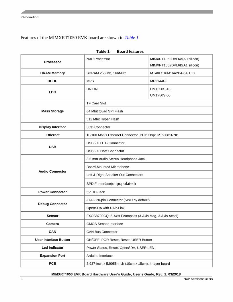
Features of the MIMXRT1050 EVK board are shown in Table 1
Table 1. Board features
Processor NXP Processor MIMXRT1052DVL6A(A0 silicon)
MIMXRT1052DVL6B(A1 silicon)
DRAM Memory SDRAM 256 Mb, 166MHz MT48LC16M16A2B4-6AIT: G
DCDC MPS MP2144GJ
LDO UNION UM1550S-18
UM1750S-00
Mass Storage
TF Card Slot
64 Mbit Quad SPI Flash
512 Mbit Hyper Flash
Display Interface LCD Connector
Ethernet 10/100 Mbit/s Ethernet Connector. PHY Chip: KSZ8081RNB
USB USB 2.0 OTG Connector
USB 2.0 Host Connector
Audio Connector
3.5 mm Audio Stereo Headphone Jack
Board-Mounted Microphone
Left & Right Speaker Out Connectors
SPDIF Interface(unpopulated)
Power Connector 5V DC-Jack
Debug Connector JTAG 20-pin Connector (SWD by default)
OpenSDA with DAP-Link
Sensor FXOS8700CQ: 6-Axis Ecompass (3-Axis Mag, 3-Axis Accel)
Camera CMOS Sensor Interface
CAN CAN Bus Connector
User Interface Button ON/OFF, POR Reset, Reset, USER Button
Led Indicator Power Status, Reset, OpenSDA, USER LED
Expansion Port Arduino Interface
PCB 3.937-inch x 5.9055-inch (10cm x 15cm), 4-layer board
Introduction
MIMXRT1050 EVK Board Hardware User’s Guide, User's Guide, Rev. 2, 03/2018
NXP Semiconductors 3
1.2. MIMXRT1050 EVK Contents
The MIMXRT1050 EVK contains the following items:
• MIMXRT1050 EVK Board
• USB Cable (Micro B)
1.3. MIMXRT1050 EVK Board revision history
• EVK Rev A: Prototype.
• EVK Rev A1/2: Pilot Board.
• EVK Rev A3/4/5:Mass Product.
NOTE
EVK Rev A, Rev A1/2/3/4/5 Boards are based on A0 silicon.
• EVKB: Mass Product.
NOTE
EVKB Boards are based on A1 silicon.
Specifications
MIMXRT1050 EVK Board Hardware User’s Guide, User's Guide, Rev. 2, 03/2018
4 NXP Semiconductors
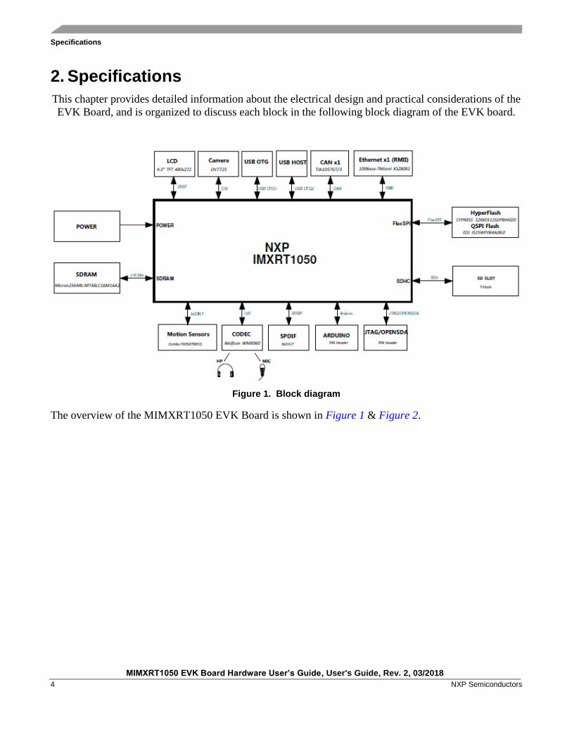
2. Specifications
This chapter provides detailed information about the electrical design and practical considerations of the
EVK Board, and is organized to discuss each block in the following block diagram of the EVK board.
Figure 1. Block diagram
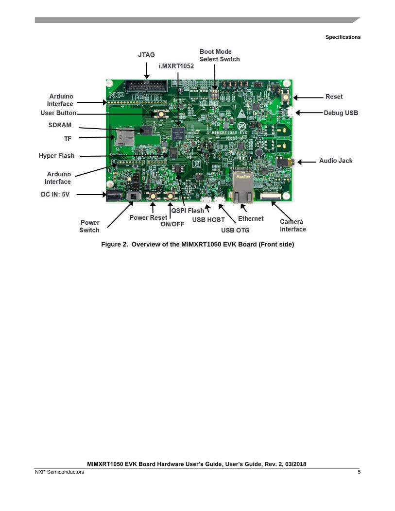
The overview of the MIMXRT1050 EVK Board is shown in Figure 1 & Figure 2.
Specifications
MIMXRT1050 EVK Board Hardware User’s Guide, User's Guide, Rev. 2, 03/2018
NXP Semiconductors 5
Figure 2. Overview of the MIMXRT1050 EVK Board (Front side)
Specifications
MIMXRT1050 EVK Board Hardware User’s Guide, User's Guide, Rev. 2, 03/2018
6 NXP Semiconductors
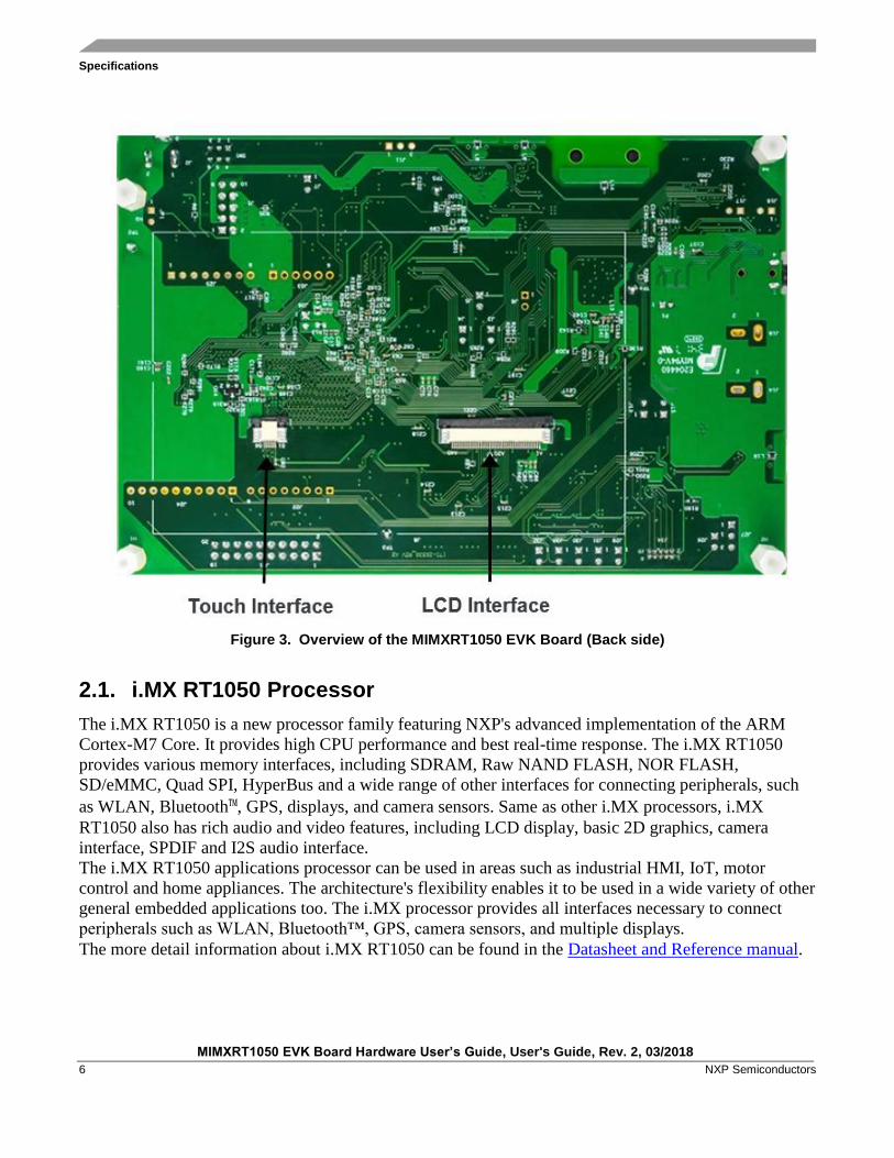
Figure 3. Overview of the MIMXRT1050 EVK Board (Back side)
2.1. i.MX RT1050 Processor
The i.MX RT1050 is a new processor family featuring NXP's advanced implementation of the ARM
Cortex-M7 Core. It provides high CPU performance and best real-time response. The i.MX RT1050
provides various memory interfaces, including SDRAM, Raw NAND FLASH, NOR FLASH,
SD/eMMC, Quad SPI, HyperBus and a wide range of other interfaces for connecting peripherals, such
as WLAN, Bluetooth™, GPS, displays, and camera sensors. Same as other i.MX processors, i.MX
RT1050 also has rich audio and video features, including LCD display, basic 2D graphics, camera
interface, SPDIF and I2S audio interface.
The i.MX RT1050 applications processor can be used in areas such as industrial HMI, IoT, motor
control and home appliances. The architecture's flexibility enables it to be used in a wide variety of other
general embedded applications too. The i.MX processor provides all interfaces necessary to connect
peripherals such as WLAN, Bluetooth™, GPS, camera sensors, and multiple displays.
The more detail information about i.MX RT1050 can be found in the Datasheet and Reference manual.
Specifications
MIMXRT1050 EVK Board Hardware User’s Guide, User's Guide, Rev. 2, 03/2018
NXP Semiconductors 7
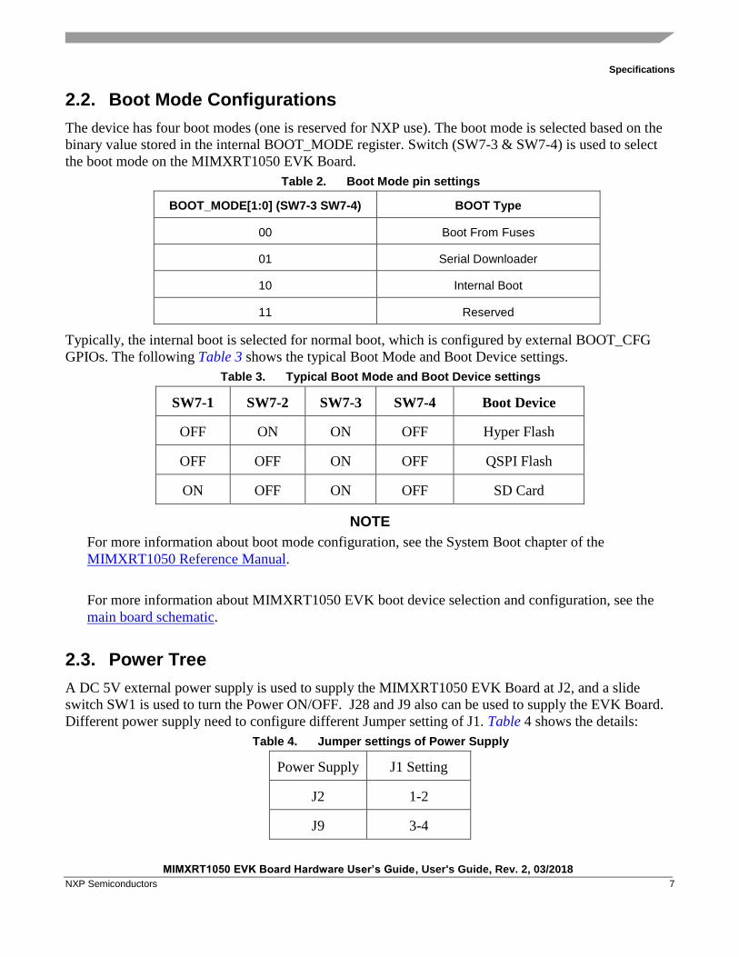
2.2. Boot Mode Configurations
The device has four boot modes (one is reserved for NXP use). The boot mode is selected based on the
binary value stored in the internal BOOT_MODE register. Switch (SW7-3 & SW7-4) is used to select
the boot mode on the MIMXRT1050 EVK Board.
Table 2. Boot Mode pin settings
BOOT_MODE[1:0] (SW7-3 SW7-4) BOOT Type
00 Boot From Fuses
01 Serial Downloader
10 Internal Boot
11 Reserved
Typically, the internal boot is selected for normal boot, which is configured by external BOOT_CFG
GPIOs. The following Table 3 shows the typical Boot Mode and Boot Device settings.
Table 3. Typical Boot Mode and Boot Device settings
SW7-1 SW7-2 SW7-3 SW7-4 Boot Device
OFF ON ON OFF Hyper Flash
OFF OFF ON OFF QSPI Flash
ON OFF ON OFF SD Card
NOTE
For more information about boot mode configuration, see the System Boot chapter of the
MIMXRT1050 Reference Manual.
For more information about MIMXRT1050 EVK boot device selection and configuration, see the
main board schematic.
2.3. Power Tree
A DC 5V external power supply is used to supply the MIMXRT1050 EVK Board at J2, and a slide
switch SW1 is used to turn the Power ON/OFF. J28 and J9 also can be used to supply the EVK Board.
Different power supply need to configure different Jumper setting of J1. Table 4 shows the details:
Table 4. Jumper settings of Power Supply
Power Supply J1 Setting
J2 1-2
J9 3-4
Specifications
MIMXRT1050 EVK Board Hardware User’s Guide, User's Guide, Rev. 2, 03/2018
8 NXP Semiconductors
J28 5-6
NOTE
For some computers’ USB, it cannot support 500ma before establishing
communication. In this case, it is recommended to replace the computer or
use the power adapter(J2) to power the EVK Board.
The power tree is shown in the following figure.
Figure 4. Power Tree
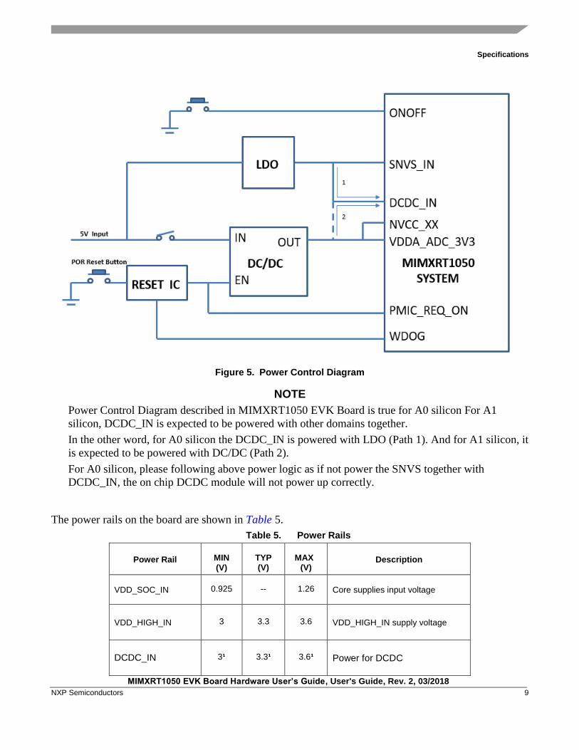
The power control logic of the MIMXRT1050 EVK board is shown in the following figure:
For A0 silicon:
• It will power up SNVS and DCDC_IN together firstly, then PMIC_REQ_ON will be switched
on to enable external DC/DC to power up other power domains.
• ON/OFF button is used to switch ON/OFF PMIC_REQ_ON to control power modes.
• RESET button and WDOG output are used to reset the system power.
For A1 silicon:
• It will power up SNVS firstly, then PMIC_REQ_ON will be switched on to enable external
DC/DC to power up other power domains.
• ON/OFF button is used to switch ON/OFF PMIC_REQ_ON to control power modes.
• RESET button and WDOG output are used to reset the system power.
Specifications
MIMXRT1050 EVK Board Hardware User’s Guide, User's Guide, Rev. 2, 03/2018
NXP Semiconductors 9
Figure 5. Power Control Diagram
NOTE
Power Control Diagram described in MIMXRT1050 EVK Board is true for A0 silicon For A1
silicon, DCDC_IN is expected to be powered with other domains together.
In the other word, for A0 silicon the DCDC_IN is powered with LDO (Path 1). And for A1 silicon, it
is expected to be powered with DC/DC (Path 2).
For A0 silicon, please following above power logic as if not power the SNVS together with
DCDC_IN, the on chip DCDC module will not power up correctly.
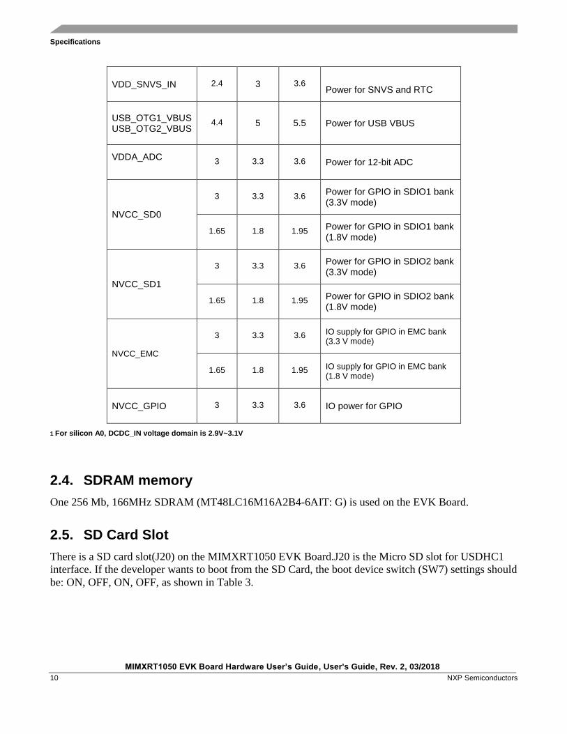
The power rails on the board are shown in Table 5.
Table 5. Power Rails
Power Rail
MIN (V)
TYP (V)
MAX
(V)
Description
VDD_SOC_IN
0.925 -- 1.26 Core supplies input voltage
VDD_HIGH_IN
3
3.3 3.6 VDD_HIGH_IN supply voltage
DCDC_IN
3¹
3.3¹ 3.6¹ Power for DCDC
Specifications
MIMXRT1050 EVK Board Hardware User’s Guide, User's Guide, Rev. 2, 03/2018
10 NXP Semiconductors
VDD_SNVS_IN
2.4
3
3.6 Power for SNVS and RTC
USB_OTG1_VBUS USB_OTG2_VBUS
4.4
5
5.5
Power for USB VBUS
VDDA_ADC
3
3.3 3.6 Power for 12-bit ADC
NVCC_SD0
3
3.3 3.6 Power for GPIO in SDIO1 bank (3.3V mode)
1.65
1.8 1.95 Power for GPIO in SDIO1 bank (1.8V mode)
NVCC_SD1
3
3.3 3.6 Power for GPIO in SDIO2 bank (3.3V mode)
1.65
1.8 1.95 Power for GPIO in SDIO2 bank (1.8V mode)
NVCC_EMC
3
3.3 3.6 IO supply for GPIO in EMC bank (3.3 V mode)
1.65
1.8 1.95 IO supply for GPIO in EMC bank (1.8 V mode)
NVCC_GPIO
3
3.3 3.6 IO power for GPIO
1 For silicon A0, DCDC_IN voltage domain is 2.9V~3.1V
2.4. SDRAM memory
One 256 Mb, 166MHz SDRAM (MT48LC16M16A2B4-6AIT: G) is used on the EVK Board.
2.5. SD Card Slot
There is a SD card slot(J20) on the MIMXRT1050 EVK Board.J20 is the Micro SD slot for USDHC1
interface. If the developer wants to boot from the SD Card, the boot device switch (SW7) settings should
be: ON, OFF, ON, OFF, as shown in Table 3.
Specifications
MIMXRT1050 EVK Board Hardware User’s Guide, User's Guide, Rev. 2, 03/2018
NXP Semiconductors 11
2.6. Hyper Flash
On the MIMXRT1050 EVK Board, there is one 512Mbit Hyper Flash device. If the developer wants to
boot from the Hyper Flash, the boot device switch (SW7) settings should be: OFF. ON, ON, OFF, as
shown in Table3.
2.7. QSPI Flash
A 64Mbit QSPI Flash is used on the MIMXRT1050 EVK Board. If the developer wants to boot from the
QSPI Flash, the boot device switch(SW7) settings should be: OFF, OFF, ON, OFF, as shown in Table3.
By default, this QSPI Flash is disabled on the EVK. To enable the onboard QSPI Flash, the settings need
to be changed.
2.7.1. EVKA Settings
Step1:
The onboard HyperFlash should be removed, otherwise it will impact the QSPI Flash read and write
timing.
Step2:
Weld 0 Ω resistor to the pad from R153 to R158.
2.7.2. EVKB Settings
For EVKB board, the onboard HyperFlash doesn’t need to remove.
Step1:
Removed resistors: R356, R361 - R366.
Step2:
Weld 0Ωresistors: R153 - R158.
2.8. Ethernet Connector
There is one Ethernet Mac controller in the MIMXRT1050 processor. The Ethernet subsystem of the
MIMXRT1050 EVK Board is provided by the KSZ8081RNB 10/100M Ethernet Transceiver (U16) and
a RJ45 (J19) with integrated Magnetic.
2.9. USB PHY Connector
The MIMXRT1050 contains 2 integrated USB 2.0 PHYs capable of connecting to USB host/device
systems at the USB low-speed (LS) rate of 1.5 Mbits/s, full-speed (FS) rate of 12 Mbits/s or at the USB
2.0 high-speed (HS) rate of 480 Mbits/s.
Specifications
MIMXRT1050 EVK Board Hardware User’s Guide, User's Guide, Rev. 2, 03/2018
12 NXP Semiconductors
2.10. Audio input / output Connector
The Audio CODEC used on the MIMXRT1050 EVK Board is Wolfson’s Low Power, high quality
Stereo Codec, WM8960.The MIMXRT1050 EVK Board include one headphone interface (J12), one
onboard MIC (P1), two speaker interfaces (J16, J17), and the SPDIF interface (J14 & J18, DNP). J12 is
a 3.5mm audio stereo headphone jack, which supports jack detect.
2.11. OpenSDA circuit (DAP-Link)
The OpenSDA circuit (CMSIS–DAP) is an open-standard serial and debug adapter. It bridges serial and
debug communications between a USB host and an embedded target processor.
CMSIS-DAP features a mass storage device (MSD) bootloader, which provides a quick and easy
mechanism for loading different CMSIS-DAP Applications such as flash programmers, run-control
debug interfaces, serial-to-USB converters, and more. Two or more CMSIS-DAP applications can run
simultaneously. For example, run-control debug application and serial-to-USB converter runs in parallel
to provide a virtual COM communication interface while allowing code debugging via CMSIS-DAP
with just single USB connection.
For the MIMXRT1050 EVK Board, J28 is the connector between the USB host and the target processor.
Jumper to serial downloader mode to use stable DAP-Link debugger function. If developer wants to
make OpenSDA going to the bootloader mode, J27 should jumper to 1-2, and press SW4 when power
on. Meanwhile, the OpenSDA supports drag/drop feature for U-Disk. First, use the seral downloader
mode and drag/drop the image file to U-Disk. Then select Hyper Flash as boot device and reset the
Board, the image will run.
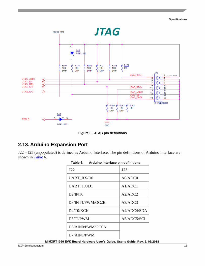
2.12. JTAG Connector
J21 is a standard 20-pin/2.54mm Box Header Connector for JTAG. The pin definitions are shown in the
following figure. Support SWD by default.
Specifications
MIMXRT1050 EVK Board Hardware User’s Guide, User's Guide, Rev. 2, 03/2018
NXP Semiconductors 13
Figure 6. JTAG pin definitions
2.13. Arduino Expansion Port
J22 – J25 (unpopulated) is defined as Arduino Interface. The pin definitions of Arduino Interface are
shown in Table 6.
Table 6. Arduino Interface pin definitions
J22 J23
UART_RX/D0 A0/ADC0
UART_TX/D1 A1/ADC1
D2/INT0 A2/ADC2
D3/INT1/PWM/OC2B A3/ADC3
D4/T0/XCK A4/ADC4/SDA
D5/TI/PWM A5/ADC5/SCL
D6/AIN0/PWM/OC0A
D7/AIN1/PWM
Specifications
MIMXRT1050 EVK Board Hardware User’s Guide, User's Guide, Rev. 2, 03/2018
14 NXP Semiconductors
J24 J25
D8/CLKO/ICP1 NC
D9/OC1A/PWM IOREF
D10/SPI_CS RESET
D11/OC2A/PWM/SPI_MOSI 3.3V
D12/SPI_MISO 5V
D13/SPI_CLK GND
GND GND
AREF VIN
D14/I2C_SDA
D15/I2C_SCL
2.14. Camera Module Connector
One parallel CSI (Camera Sensor Interface) is supported by the i.MX RT1050. There is a Camera
Module Connector (J35) on the MIMXRT1050 EVK Board. The CA031C based on OV7725 can be
used directly.
2.15. User Interface Switch
There are four user interface switches on the MIMXRT1050 EVK Board. Their functionality is as
below.
2.15.1. Power Switch
SW1 is a slide switch to control the power of the MIMXRT1050 EVK Board when the power supply is
from J2. The function of this switch is listed below:
• Sliding the switch to the ON position connects the 5V power supply to the Evaluation board
main power system.
• Sliding the switch to OFF position immediately removes all power from the board.
2.15.2. ON/OFF Button
SW2 is the ON/OFF button for MIMXRT1050 EVK Board. A short pressing in OFF mode causes the
internal power management state machine to change state to ON. In ON mode, a short pressing
Specifications
MIMXRT1050 EVK Board Hardware User’s Guide, User's Guide, Rev. 2, 03/2018
NXP Semiconductors 15
generates an interrupt (intended to be a software-controllable(power-down). An approximate 5 seconds
or more pressing causes a forced OFF. Both boot mode inputs can be disconnected.
2.15.3. Reset Button
There are two Reset Button on the EVK Board. SW3 is the Power Reset Button. Pressing the SW3 in the
Power On state will force to reset the system power except SNVS domain. The Processor will be
immediately turn off and reinitiate a boot cycle from the Processor Power Off state. SW4 is Reset
Button.
2.15.4. USER Button
SW8 is the USER Button(GPIO5-00) for developers using. Pressing can produce changes in high and
low levels.
2.16. Sensor
U32 on the EVK Board is a 6-Axis Ecompass (3-Axis Mag, 3-Axis Accel) sensor FXOS8700CQ. The
Ecompass is connected to i.MX RT1050 I2C1 port.
2.17. User Interface LED Indicator
There are four LED status indicators located on the EVK Board. The functions of these LEDs include:
• Main Power Supply(D3)
Green: DC 5V main supply is normal.
Red: J2 input voltage is over 5.6V.
Off: the board is not powered.
• Reset RED LED(D15)
• OpenSDA LED(D16)
• USER LED(D18)
2.18. LCD Interface
The enhanced Liquid Crystal Display Interface (eLCDIF) is a general purpose display controller.
The eLCDIF block supports the following:
• Displays that support moving pictures and require the RGB interface mode (DOTCLK interface).
The eLCDIF provides fully programmable functionality to supported interfaces:
• Bus master interface to source frame buffer data for display refresh.
• 8/16/18/24/32 bit LCD data bus support available depending on I/O mux options.
• Programmable timing and parameters for DOTCLK LCD interfaces.
Contents of the Evaluation Kit
MIMXRT1050 EVK Board Hardware User’s Guide, User's Guide, Rev. 2, 03/2018
16 NXP Semiconductors
If developers want to use LCD, NXP provides an optional LCD module RK043FN02H-CT which has a
4.3 inches touch-screen and supports a resolution of up to 480*3(RGB)*272. This module contains two
FPC cables. The LCD interface can be connected to J8(A1-A40) and the CPT interface can be connected
to J8(B1-B6). LCD modules can be purchased from the NXP website.
3. PCB Information
The MIMXRT1050 EVK Board is made using standard 4-layer technology. The material used was FR-
4. The PCB stack-up information is shown in Table 7.
Table 7. Board stack-up information
Layer Description Copper(Oz) Dielectric Thickness(mil)
1 Signal 1 —
Dielectric — 3
2 GND 1 —
Dielectric — 52
3 Power 1 —
Dielectric — 3
4 Signal 1 —
4. EVK Design Files
The schematics, layout files, and gerber files (including Silkscreen) can be downloaded from
nxp.com/MIMXRT1050-EVK
5. Contents of the Evaluation Kit Table 8. EVK contents
Item Description
EVK Board EVK Board with processor, memory, interfaces, etc
USB Cable USB cable (Micro-B to Standard-A)
NOTE
Power adaptor, Micro SD Card, LCD Module and Camera Module are not standard parts of the
Evaluation Kit.
Revision history
MIMXRT1050 EVK Board Hardware User’s Guide, User's Guide, Rev. 2, 03/2018
NXP Semiconductors 17
6. Revision history
Table 9 summarizes the changes made to this document since the initial release.
Table 9. Revision history
Revision number Date Substantive changes
0 08/2017 Initial release
1 11/2017 References/links have been
completed
2 03/2018 Add(Update) information for RT1050
silicon A1
Document Number: MIMXRT1050EVKHUG Rev. 2
03/2018
How to Reach Us:
Home Page:
nxp.com
Web Support:
nxp.com/support
Information in this document is provided solely to enable system and software
implementers to use NXP products. There are no express or implied copyright licenses
granted hereunder to design or fabricate any integrated circuits based on the
information in this document. NXP reserves the right to make changes without further
notice to any products herein.
NXP makes no warranty, representation, or guarantee regarding the suitability of its
products for any particular purpose, nor does NXP assume any liability arising out of
the application or use of any product or circuit, and specifically disclaims any and all
liability, including without limitation consequential or incidental damages. “Typical”
parameters that may be provided in NXP data sheets and/or specifications can and do
vary in different applications, and actual performance may vary over time. All operating
parameters, including “typicals,” must be validated for each customer application by
customer’s technical experts. NXP does not convey any license under its patent rights
nor the rights of others. NXP sells products pursuant to standard terms and conditions
of sale, which can be found at the following address: nxp.com/SalesTermsandConditions.
NXP, the NXP logo, NXP SECURE CONNECTIONS FOR A SMARTER WORLD,
Freescale, the Freescale logo are the trademarks of NXP B.V. All other product or
service names are the property of their respective owners.
Arm, the Arm logo, and Cortex are registered trademarks of Arm Limited (or its
subsidiaries) in the EU and/or elsewhere.. All rights reserved.
© 2018 NXP B.V.