Accepted for publication (shorter version), IEEE Trans. On VLSI, 2006 Minimal Energy Asynchronous Dynamic Adders Ilya Obridko and Ran Ginosar VLSI Systems Research Center, Technion—Israel Institute of Technology, Haifa 32000, Israel [[email protected], [email protected]] Abstract In battery-operated portable or implantable digital devices, where battery life needs to be maximized, it is necessary to minimize not only power consumption but also energy dissipation. Typical energy optimization measures include voltage reduction and operating at the slowest possible speed. We employ additional methods, including hybrid asynchronous dynamic design to enable operating over a wide range of battery voltage, aggregating large combinational logic blocks, and transistor sizing and reordering. We demonstrate the methods on simple adders, and discuss extension to other circuits. Three novel adders are proposed and analyzed: A two-bit PTL adder and two dynamic two-bit adders. Circuit simulations on a 0.18μm process at low voltage show that leakage energy is below 1% and that short-circuit energy depends on circuit topology and can be as high as 50% of total energy when operating at low voltage and low fanout. The proposed adders achieve up to 40% energy savings relative to previously published results, while also operating faster. 1 Introduction Certain digital battery-operated portable or implanted systems require maximum battery life. To achieve that goal, the designer needs to minimize energy dissipation (rather than optimizing for low power). One useful means is to allow operating at the slowest possible computational speed, and this is possible in devices such as hearing aids in which the computational requirements are limited. Another obvious method is operating at the lowest possible supply voltage. In addition, many batteries provide a varying level of voltage over their lifetime, and the circuit be better designed to accommodate a wide range of supply voltages. Such voltage variation results in wide delay variation. Common approaches to low power and low energy design include the following. Asynchronous, delay- insensitive circuits [1]—[13] enable operation over a wide voltage range. Some of them employ dual rail logic [1]—[4], others use single-rail design [5]—[9][26], while still others combine single- and dual-rail for further energy minimization [10]—[13]. General purpose programmable instruction-execution based processors are avoided when possible, to eliminate the energy required for instruction fetch and decode [1][2][14][15]. A variety of low power / low energy circuit techniques are proposed in [14][16]—[20]. Adders are representative of signal processing architectures, and the results can be extended to other data path circuits. Fast static, bundled-data asynchronous adders are described in [26][27]. Both papers describe various speed-up techniques that may trade-off power efficiency for speed. These techniques are best avoided when the lowest energy per computation is sought. Thus, we focus on ripple-carry adders. References [26][27] also indicate power and energy advantages of asynchronous adders, but are inconclusive regarding whether static or dynamic circuits would dissipate lower energy. In this paper we focus on dynamic adders. We consider some previously published low energy dynamic adders [11][21]—[23] and apply a number of transformations to them, resulting in three novel architectures. The transformations include various topology changes, the aggregation of full-adders into larger combinational circuits, the combination of dual- and single-rail asynchronous logic, proper transistor sizing, and transistor reordering to minimize the charge drawn from the supply. We operate the circuits at the lowest possible voltage, and consider their operation over a wide range of voltages. We discuss four previously published low power adders in Section 2, and introduce three novel adders in Section 3. Circuit simulation analysis on a 0.18μm process is presented in Section 4, where we show that leakage energy is negligible, short-circuit energy can be significant depending on circuit topology, and in
Transcript
Accepted for publication (shorter version), IEEE Trans. On VLSI, 2006
Minimal Energy Asynchronous Dynamic Adders Ilya Obridko and Ran Ginosar
VLSI Systems Research Center, Technion—Israel Institute of Technology, Haifa 32000, Israel
Abstract In battery-operated portable or implantable digital devices, where battery life needs to be maximized, it is necessary to minimize not only power consumption but also energy dissipation. Typical energy optimization measures include voltage reduction and operating at the slowest possible speed. We employ additional methods, including hybrid asynchronous dynamic design to enable operating over a wide range of battery voltage, aggregating large combinational logic blocks, and transistor sizing and reordering. We demonstrate the methods on simple adders, and discuss extension to other circuits. Three novel adders are proposed and analyzed: A two-bit PTL adder and two dynamic two-bit adders. Circuit simulations on a 0.18μm process at low voltage show that leakage energy is below 1% and that short-circuit energy depends on circuit topology and can be as high as 50% of total energy when operating at low voltage and low fanout. The proposed adders achieve up to 40% energy savings relative to previously published results, while also operating faster.
1 Introduction Certain digital battery-operated portable or implanted systems require maximum battery life. To achieve that goal, the designer needs to minimize energy dissipation (rather than optimizing for low power). One useful means is to allow operating at the slowest possible computational speed, and this is possible in devices such as hearing aids in which the computational requirements are limited. Another obvious method is operating at the lowest possible supply voltage. In addition, many batteries provide a varying level of voltage over their lifetime, and the circuit be better designed to accommodate a wide range of supply voltages. Such voltage variation results in wide delay variation.
Common approaches to low power and low energy design include the following. Asynchronous, delay-insensitive circuits [1]— [13] enable operation over a wide voltage range. Some of them employ dual rail logic [1]— [4], others use single-rail design [5]— [9] [26], while still others combine single- and dual-rail for further energy minimization [10]— [13]. General purpose programmable instruction-execution based processors are avoided when possible, to eliminate the energy required for instruction fetch and decode [1] [2] [14] [15]. A variety of low power / low energy circuit techniques are proposed in [14] [16]— [20].
Adders are representative of signal processing architectures, and the results can be extended to other data path circuits. Fast static, bundled-data asynchronous adders are described in [26] [27]. Both papers describe various speed-up techniques that may trade-off power efficiency for speed. These techniques are best avoided when the lowest energy per computation is sought. Thus, we focus on ripple-carry adders. References [26] [27] also indicate power and energy advantages of asynchronous adders, but are inconclusive regarding whether static or dynamic circuits would dissipate lower energy. In this paper we focus on dynamic adders.
We consider some previously published low energy dynamic adders [11] [21]— [23] and apply a number of transformations to them, resulting in three novel architectures. The transformations include various topology changes, the aggregation of full-adders into larger combinational circuits, the combination of dual- and single-rail asynchronous logic, proper transistor sizing, and transistor reordering to minimize the charge drawn from the supply. We operate the circuits at the lowest possible voltage, and consider their operation over a wide range of voltages.
We discuss four previously published low power adders in Section 2, and introduce three novel adders in Section 3. Circuit simulation analysis on a 0.18μm process is presented in Section 4, where we show that leakage energy is negligible, short-circuit energy can be significant depending on circuit topology, and in
2
general our Minimum Energy Dual-Bit Dynamic adder achieves up to 40% energy savings while operating up to 60% faster than the other adders.
2 Existing Asynchronous Low Energy Dynamic Adders Common fast adder architectures, such as carry-select, carry-look-ahead and parallel-prefix adders consume excessive energy for the sake of speed, due to circuits that speed up the logic and introduce additional transitions. The slower ripple-carry adder (comprising only full adder cells) typically consumes the least amount of energy per addition thanks to the absence of “redundant” logic that is used in other adder architectures to speed up and parallelize calculations. The energy dissipation can be further minimized by using larger blocks of logic. For instance, each basic cell can add two or more pairs of bits at once. Larger blocks reduce wire and transistor counts, thus minimizing the number of transitions.
Asynchronous adders can be implemented employing either bundled-data static circuits, or dynamic ones. Bundled data asynchronous adders were described in [26], showing potential for logic size minimization and low power. Comparison of the two types was described in [27], showing similar energy consumption: The dynamic adder had fewer transistors and less capacitance to charge, because only one PMOS transistor is used for each logic gate. Another example is Martin’s adder [21], which is more energy hungry due to the larger number of PMOS transistors. When the delay line is added to a static adder (to make it bundled data), its energy advantage is further diminished. If the static logic is not hazard-free, glitches may dissipate additional energy. On the other hand, dynamic dual rail logic dissipates energy on pre-charging and on completion detection. Thus, there is no clear winner that always dissipates less energy than the other, and a detailed comparison is recommended when the two approaches are evaluated. In this paper we focus on dynamic asynchronous adders.
In this section we analyze four previously proposed asynchronous dynamic low energy full-adder cells: A dynamic dual-rail adder, a dynamic hybrid adder combining dual and single rail encodings, a dual-bit dynamic adder, and a PTL adder.
2.1 A Dynamic Dual-rail Adder Martin’s adder [21] minimizes the number of signals that must be considered for completion detection [21] based on the evaluation of guaranteed dependencies. Note that none of the full adder (FA) cells can complete the calculation before the arrival of the Carry-in signal from the previous stage. Thus, if the S and Cout signals are valid, it means that Carry-in is valid, and current S and Cout provide indication also for Carry-in. In an n-bit adder, it is sufficient to observe the n sum outputs and the final carry-out in order to detect completion. The drawback of this method is that the Completion Detection (CD) logic is organized as a tree having n inputs (n being the number of bits) and hence it grows at a rate of O(n).
Figure 1. Martin’s adder circuits
Martin’s adder ( Figure 1) employs dynamic pre-charged dual-rail logic. Note that each complex gate requires multiple PMOS transistors in its pre-charge path. To minimize the size of the completion detection
3
and pre-charge logic, it uses weak indication. Due to using dual-rail logic, this adder consumes more energy than the remaining circuits below.
Another possible asynchronous dual rail adder can be implemented using DIMS (Delay Insensitive Minterm Synthesis) logic [13]. But since DIMS is based on strong indication, it dissipates more energy and hence it is not considered in this paper.
2.2 A Dynamic Single-Bit Adder Nielsen’s [11] [12] ripple carry adder produces only a single-rail output s.t for the sum, since completion is indicated by cout signals. This is a hybrid approach, where sum is single-rail, and the inputs, carry in and carry out are all dual-rail.
Figure 2. Nielsen’s dynamic adder schematics
It can be observed in Figure 2 that the adder is reset by Req, which is common to all stages. This allows quick execution of the return-to-zero part of the handshake. Likewise, when Req rises, all the stages in the chain start their calculation simultaneously. sum1,2,3 and cout1,2,3 are complex gates consisting merely of NMOS pull down logic. Using Req signal allows reducing the Reset logic size, using a single PMOS transistor per complex gate, and consequently dissipating less energy than Martin’s Adder.
A detailed CMOS implementation of the cell circuit is described in Figure 3. A low output is retained by the keeper transistor. The circuit is based on Nielsen’s Adder but we have eliminated some logically redundant transistors that were originally included for timing symmetry but consumed more energy.
2.3 A Dynamic Dual-Bit Adder Chong [22] describes a low transition count, low energy adder based on dual-bit adder cells. Similar to Nielsen’s adder, completion detection is based only on the last dual-rail CarryOut signal. All Sum signals are single-rail ( Figure 4). The dual-bit adder circuit is shown in Figure 5.
2.4 A PTL Single-Bit Adder PTL (Pass Transistor Logic) is claimed to provide a low energy solution for arithmetic functions [19] [23], because arithmetic functions include many XOR gates, and PTL implements XOR gates in an efficient manner. PTL circuits supposedly dissipate low energy thanks to using a small number of pass transistors, which are usually NMOS.
4
Figure 3. Nielsen’s dynamic one-bit adder
Figure 4. Chong’s adder schematics
Figure 5. Chong’s dynamic dual-bit adder
Another reason that PTL circuits dissipate low energy is the absence of VDD-to-GND paths, thus eliminating short-circuit energy dissipation during slow transitions. The voltage degradation (VDD-VTn) associated with NMOS PTL further reduces energy thanks to reducing the charge being transferred. This is compromised somewhat by the need for inverters and buffers for swing restoration. In addition, the fact that the same charge is transferred through long NMOS chains also contributes to energy savings.
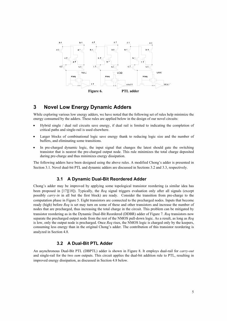
We examine an asynchronous PTL full adder circuit following [19], implementing dual rail Cout and single rail Sum ( Figure 6). The output is pre-charged by Req; when Req=0 all outputs show empty tokens, and Req=1 produces valid outputs. The output is separated from the evaluation PTL circuit with a path transistor, also driven by Req, to prevent contention (and short-circuit current) on the pre-charged node. Completion is detected by Cout.
5
Figure 6. PTL adder
3 Novel Low Energy Dynamic Adders While exploring various low energy adders, we have noted that the following set of rules help minimize the energy consumed by the adders. These rules are applied below in the design of our novel circuits:
• Hybrid single / dual rail circuits save energy, if dual rail is limited to indicating the completion of critical paths and single-rail is used elsewhere.
• Larger blocks of combinational logic save energy thank to reducing logic size and the number of buffers, and eliminating some transitions.
• In pre-charged dynamic logic, the input signal that changes the latest should gate the switching transistor that is nearest the pre-charged output node. This rule minimizes the total charge deposited during pre-charge and thus minimizes energy dissipation.
The following adders have been designed using the above rules. A modified Chong’s adder is presented in Section 3.1. Novel dual-bit PTL and dynamic adders are discussed in Sections 3.2 and 3.3, respectively.
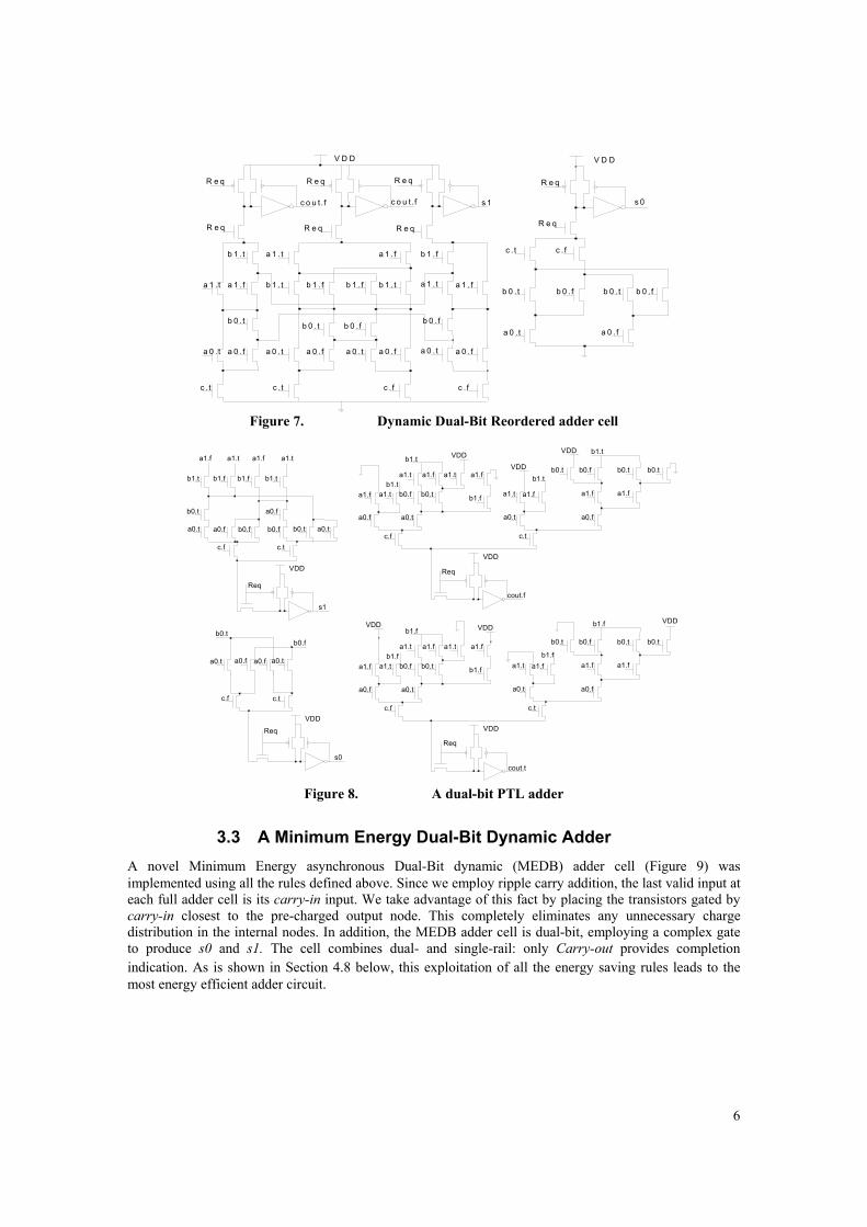
3.1 A Dynamic Dual-Bit Reordered Adder Chong’s adder may be improved by applying some topological transistor reordering (a similar idea has been proposed in [17] [18]). Typically, the Req signal triggers evaluation only after all signals (except possibly carry-in in all but the first block) are ready. Consider the transition from pre-charge to the computation phase in Figure 5. Eight transistors are connected to the precharged nodes. Inputs that become ready (high) before Req is set may turn on some of these and other transistors and increase the number of nodes that are precharged, thus increasing the total charge in the circuit. This problem can be mitigated by transistor reordering as in the Dynamic Dual-Bit Reordered (DDBR) adder of Figure 7. Req transistors now separate the precharged output node from the rest of the NMOS pull-down logic. As a result, as long as Req is low, only the output node is precharged. Once Req rises, the NMOS logic is charged only by the keepers, consuming less energy than in the original Chong’s adder. The contribution of this transistor reordering is analyzed in Section 4.8.
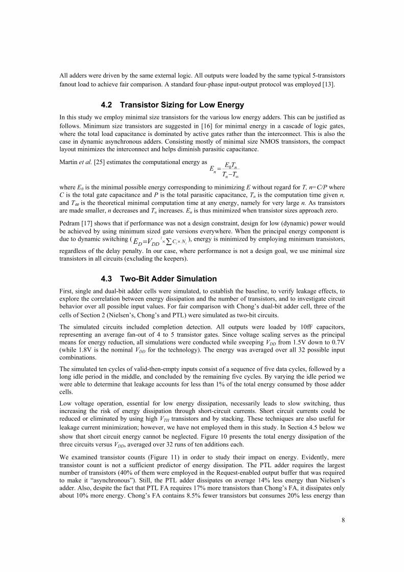
3.2 A Dual-Bit PTL Adder An asynchronous Dual-Bit PTL (DBPTL) adder is shown in Figure 8. It employs dual-rail for carry-out and single-rail for the two sum outputs. This circuit applies the dual-bit addition rule to PTL, resulting in improved energy dissipation, as discussed in Section 4.8 below.
6
c . fc . fc . tc . t
a 0 .t a 0 .f a 0 . t a 0 .f
c o u t . f c o u t. f s 1
V D D
a 0 .t a 0 . f a 0 .t a 0 . f
b 0 .t b 0 .f b 0 .fb 0 .t
a 1 .t a 1 .f b 1 . t b 1 .f b 1 .f b 1 . t a 1 .t a 1 . f
a 1 . tb 1 .t a 1 . f b 1 .f
R e q R e q R e q
s 0
V D D
a 0 .t a 0 .f
b 0 . t b 0 .f b 0 .t b 0 . f
c . t c . f
R e q
R e q R e q R e q R e q
Figure 7. Dynamic Dual-Bit Reordered adder cell
c.tc.f
s0
VDD
Req
c.tc.f
a0.t a0.f
cout.f
VDD
Req
c.tc.f
cout.t
s1
VDD
Req
a0.ta0.f
a1.f b0.f
b1.t
b0.ta1.t
a1.fa1.f
b1.f
b1.tb1.f b1.f
a1.f
b1.tb1.t
a1.t
b0.t
b0.t a0.ta0.t b0.fa0.f
a0.f
b0.f
a0.f a0.t
b0.tb0.f
a1.f a1.t
a0.fa0.t
a1.t
b1.t
a1.f
b0.t
a1.f a1.f
a1.t a1.t
VDDVDD
VDD
b0.f b0.t b0.t
c.tc.f
VDD
Req
a0.ta0.f
a1.f b0.f
b1.f
b0.ta1.t
a1.fa1.f
b1.f
b1.f
a0.fa0.t
a1.tb1.f
a1.f
b0.t
a1.f a1.f
a1.t a1.t
VDD VDD
b0.f b0.t b0.t
b1.t
b1.fVDD
Figure 8. A dual-bit PTL adder
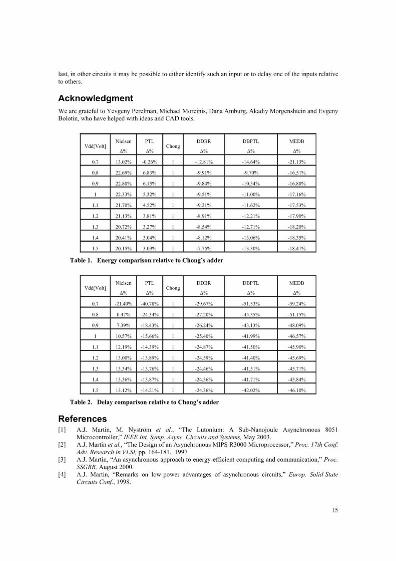
3.3 A Minimum Energy Dual-Bit Dynamic Adder A novel Minimum Energy asynchronous Dual-Bit dynamic (MEDB) adder cell ( Figure 9) was implemented using all the rules defined above. Since we employ ripple carry addition, the last valid input at each full adder cell is its carry-in input. We take advantage of this fact by placing the transistors gated by carry-in closest to the pre-charged output node. This completely eliminates any unnecessary charge distribution in the internal nodes. In addition, the MEDB adder cell is dual-bit, employing a complex gate to produce s0 and s1. The cell combines dual- and single-rail: only Carry-out provides completion indication. As is shown in Section 4.8 below, this exploitation of all the energy saving rules leads to the most energy efficient adder circuit.
7
c.t
a0.f
c.f
a0.t
s0
VDD
Req
c.tc.f
b0.t b0.f
cout.f
c.tc.f
cout.t
s1
a1.t b1.t
b1.t
a1.t
b0.t
a0.t
a1.t
b0.t
b1.t
c.f c.t
a0.t a0.fa0.f
a1.f b0.f
b1.f
b1.f b0.f
a1.f
a1.f
a1.f
b1.fb0.f
a0.f
b1.f
b1.f b1.f
a1.f a1.f
b1.tb1.t
a1.ta1.t
b0.t
b0.t a0.ta0.t b0.fa0.f
a0.f
b0.f
b0.f b0.t
Req
VDD
Req
Req
VDD
Req
Req
VDD
Req
Req
Figure 9. Minimum energy dual-bit dynamic adder
4 Simulation Results
4.1 Simulation Methodology All adders were designed using the same 0.18μm TSMC CMOS process and simulated using Cadence Spectre. We chose that process because the leakage and variations in delay and process parameters in 0.18μm and older technologies can be ignored, as opposed to newer technologies such as 90 and 65 nm. Moreover, due to high leakage, using newer processes may be less advantageous in “slow” applications where the idle time is very long.
The adders were simulated under various combinations of supply voltage, capacitive load and input values. The conditions and the assumptions were the same for all simulated circuits. Supply voltage was varied from 1.5V to 0.7V (while the nominal supply voltage is 1.8V). Capacitive loads represented fan-out of 1-10 gates. A set of one hundred random input values was applied in all simulations.
Delay and energy per computation cycle for each input vector were recorded, and averaged over the 100 random input vectors. While general purpose computing applications can favor small numbers (as shown in [28]), this may not be the case in DSP applications where special purpose low-energy circuits are desirable, such as in hearing aids and medical implantable devices. In addition, when dual-rail circuits are used, all inputs and outputs are reset each evaluation cycle, eliminating correlation between vectors. Consequently, we have opted for random inputs.
All adders were simulated using the same environment: The same interface circuit drives all the inputs, the supply voltages are the same, and the output loads are the same. The same completion detection was used for all circuits.
The adders are compared based on transistor level simulations. No layout was performed, and no wire parasitics are included. The transistor models, however, include all transistor parasitic parameters. In ripple carry adder circuits the wires are short, because most of the transistors are NMOS and layout area utilization is high. Most of the adders studied in this paper have a similar structure, leading to similar total wire length. Thus, topology and fanout constitute the principal differences when comparing the adders.
8
All adders were driven by the same external logic. All outputs were loaded by the same typical 5-transistors fanout load to achieve fair comparison. A standard four-phase input-output protocol was employed [13].
4.2 Transistor Sizing for Low Energy In this study we employ minimal size transistors for the various low energy adders. This can be justified as follows. Minimum size transistors are suggested in [16] for minimal energy in a cascade of logic gates, where the total load capacitance is dominated by active gates rather than the interconnect. This is also the case in dynamic asynchronous adders. Consisting mostly of minimal size NMOS transistors, the compact layout minimizes the interconnect and helps diminish parasitic capacitance.
Martin et al. [25] estimates the computational energy as 0 n
nn
E TET T∞
=−
where E0 is the minimal possible energy corresponding to minimizing E without regard for T, n=C/P where C is the total gate capacitance and P is the total parasitic capacitance, Tn is the computation time given n, and T∞ is the theoretical minimal computation time at any energy, namely for very large n. As transistors are made smaller, n decreases and Tn increases. En is thus minimized when transistor sizes approach zero.
Pedram [17] shows that if performance was not a design constraint, design for low (dynamic) power would be achieved by using minimum sized gate versions everywhere. When the principal energy component is due to dynamic switching ( 2
i iC ND DDE V × ×= ∑ ), energy is minimized by employing minimum transistors,
regardless of the delay penalty. In our case, where performance is not a design goal, we use minimal size transistors in all circuits (excluding the keepers).
4.3 Two-Bit Adder Simulation First, single and dual-bit adder cells were simulated, to establish the baseline, to verify leakage effects, to explore the correlation between energy dissipation and the number of transistors, and to investigate circuit behavior over all possible input values. For fair comparison with Chong’s dual-bit adder cell, three of the cells of Section 2 (Nielsen’s, Chong’s and PTL) were simulated as two-bit circuits.
The simulated circuits included completion detection. All outputs were loaded by 10fF capacitors, representing an average fan-out of 4 to 5 transistor gates. Since voltage scaling serves as the principal means for energy reduction, all simulations were conducted while sweeping VDD from 1.5V down to 0.7V (while 1.8V is the nominal VDD for the technology). The energy was averaged over all 32 possible input combinations.
The simulated ten cycles of valid-then-empty inputs consist of a sequence of five data cycles, followed by a long idle period in the middle, and concluded by the remaining five cycles. By varying the idle period we were able to determine that leakage accounts for less than 1% of the total energy consumed by those adder cells.
Low voltage operation, essential for low energy dissipation, necessarily leads to slow switching, thus increasing the risk of energy dissipation through short-circuit currents. Short circuit currents could be reduced or eliminated by using high VTH transistors and by stacking. These techniques are also useful for leakage current minimization; however, we have not employed them in this study. In Section 4.5 below we show that short circuit energy cannot be neglected. Figure 10 presents the total energy dissipation of the three circuits versus VDD, averaged over 32 runs of ten additions each.
We examined transistor counts ( Figure 11) in order to study their impact on energy. Evidently, mere transistor count is not a sufficient predictor of energy dissipation. The PTL adder requires the largest number of transistors (40% of them were employed in the Request-enabled output buffer that was required to make it “asynchronous”). Still, the PTL adder dissipates on average 14% less energy than Nielsen’s adder. Also, despite the fact that PTL FA requires 17% more transistors than Chong’s FA, it dissipates only about 10% more energy. Chong’s FA contains 8.5% fewer transistors but consumes 20% less energy than
9
the (single-bit) dynamic FA, thanks to producing only one carry-out signal. The dynamic FA calculates a carry-out signal per every bit, thus dissipating more energy.
We can learn from the simulations ( Figure 10) that Chong’s adder dissipates the least amount of energy. PTL dissipates a bit more, but less than Nielsen’s FA. All circuits demonstrate robustness to a wide variation of voltage levels. Chong’s FA produces the best result thanks to its dual-bit structure, reducing the logic size, eliminating redundant wiring and consequentially reducing the number of transitions. These observations provide a strong incentive to design larger blocks of logic in order to gain maximal energy reduction.
Average Energy vs. VDD
0.300.500.700.901.101.301.501.701.902.10
0.6 0.8 1 1.2 1.4
VDD [V]
Ever
gy [p
Joul
e]
NIELSEN CHONG PTL Figure 10. Two-bit adders’ simulation result
Tr a nsi st or Count f or D ua l - bi t A dde r
45
50
55
60
65
NIELSEN CHONG PTL
Figure 11. Two-bit adders’ transistor count
4.4 32 Bit Adder Simulation In order to get more precise results of energy and time measurements, more complex structures have to be simulated. The circuit we chose is 32 bit ripple-carry adder (RCA). Different two-bit adders were used as a base of 32 bit RCA along with regular full-adder cells. Three existing adders (Chong, Dynamic and PTL) and three novel adders (a dual-bit reordered, a dual-bit PTL and minimum energy dynamic adders) were described in Sections 2 and 3, respectively.
The simulation environment was the same as for two-bit adders (Section 4.1), except for the timing diagram–only one cycle was used to assess delay (T) and energy (E) per calculation. We also consider ET and ET2, as discussed in Section 4.6.
4.4.1 Energy Comparison Figure 12 and Table 1 show the energy consumption of the six adders. One can observe that the simple transistor reordering in Chong’s adder leads to energy reduction of about 10%. Using dual-bit PTL cells rather than single-bit ones results in 15% less energy. The advantage of larger blocks in dynamic adders is even higher: Chong’s adder consumes 20% less energy than Nielsen’s.
The novel DBPTL adder requires less energy than Chong’s, and the novel MEDB adder consumes even less energy. The latter was designed following all the rules proposed in Section 3. The MEDB adder dissipates 20% less energy than Chong’s, although it is based on the same set of formulas [22]. This advantage is achieved thanks to reducing the pre-charged capacitance and, consequently, the amount of charge deposited during the pre-charge stage. The reason for the difference in energy between the DBPTL and MEDB adders is as follows: While PTL is typically optimized for XOR gates, two-bit adders require either OR/NOR or AND/NAND gates rather than XOR, rendering DBPTL somewhat less energy efficient than the MEDB adder.
4.4.2 Delay Comparison Figure 13 and Table 2 depict the delay of all simulated adders, showing that the novel MEDB adder is the fastest one. This is thanks to the reduced amount of charge that is deposited during pre-charge and removed during evaluation. Note that this is the same argument that led to the same circuit being the most energy
10
efficient! MEDB is 50% faster than Chong’s adder thanks to transistor reordering, and 65% faster than Nielsen’s thanks to the dual-bit architecture.
DDBR adder operates 25% faster than the original Chong adder. The dual-bit PTL saves 25% time compared to the single-bit PTL adder.
32 bit adders' energy measurements
0.00E+00
5.00E-13
1.00E-12
1.50E-12
2.00E-12
2.50E-12
0.7 0.9 1.1 1.3 1.5
Vdd[V]
ener
gy[J
oule
]
NIELSENPTLCHONGDDBRDBPTLMEDB
Figure 12. 32-bit adders’ energy simulation result
32 bit adders' delay measurements
1.00E-09
1.00E-08
1.00E-07
1.00E-060.7 0.9 1.1 1.3 1.5
Vdd[V]
dela
y[s]
NIELSEN
PTL
CHONG
DDBR
DBPTL
MEDB
Figure 13. 32-bit adders’ delay simulation result
4.5 Short Circuit Energy Short-circuit (SC) energy has typically been ignored or estimated as a fixed percentage of the dynamic energy [14] [17] when transition times at the input and output ports of a gate are about equal. In addition, while dynamic energy is perceived as quadratically dependent on voltage, SC energy is considered to be a linear function of the supply voltage. However, it appears that in circuits with low fan-out, those general guidelines should be revisited.
We measured the simulated SC energy on a chain of inverters in order to estimate the portion of SC in the total energy dissipation of low-energy adders. The inverter chain generates a “typical” slope at the input of the measured gate, and its output is loaded by varying levels of fan-out, from one to ten gates. Switching energy depends linearly on fan-out, while short-circuit energy is almost independent of the output load. It is evident that at low fan-out, SC energy is close in magnitude to the switching energy. In circuits where most fan-out levels are low, it is hence unrealistic to consider SC energy to be less than 10% of the total dissipated energy [14], irrespective of the supply voltage. At high fan-out, the switching energy depends approximately quadratically on voltage, and the SC energy appears to be negligible. At low fan-out, the two energy components are about equal in this voltage range, rather than exhibiting respective quadratic and linear dependence on voltage. As summarized in Figure 14, short circuit energy (at least in the case of inverters) constitutes a certain portion of total energy, depending on fan-out but independent of voltage. At
11
fan-out levels of 1-4 (typical in the adder circuits discussed above), short circuit energy is 20%-40% of total energy dissipation.
Short circuit energy evaluation in adders is more complicated, but in general the adder can be designed to minimize SC energy. First, the higher transistor stacks result in lower short circuit currents. Second, it is feasible to reduce the probability of a short circuit path; for instance, in the MEDB adder, the carry in signal (which drives only an NMOS gate) is designed to arrive last (after the rising transition of Request).
Short Circuit Energy
0%10%20%30%40%50%
1 2 3 4 5 6 7 8 9 10Fan-Out
Perc
ent
Figure 14. Short circuit energy portion vs. fan-out
4.6 ET and ET2 Comparison Martin et al. [25] suggest optimizing ET2 instead of minimizing either component separately, because in CMOS ET2 is roughly independent of the supply voltage over a wide range. This is based on the observation that E=CV2 and the gate delay T ∝ C/V. Thus, ET2 ∝ C3, independent of V. Once optimized, energy and delay can be freely traded off against each other through supply-voltage adjustment.
Observing the graphs of ET2 ( Figure 15), note that the graphs are not as flat in this voltage range as expected. This is due to the fact that we operate at voltage levels significantly lower than nominal values, causing the following deviations. First, we operate the transistors deep into their triode region near cutoff, rather than in their normal saturation or cutoff modes. Second, the ET2 model assumes that VTH
scales with the supply voltage, but we consider normal VTH transistors regardless of the reduced voltage. Third, while energy is indeed proportional to CV2, as supported by simulation, the simulated delay is not linear in 1/V. Last, the ET2 model ignores short-circuit and leakage energy, but we show in Section 4.5 above that in low fan-out cases short-circuit energy is significant. Thus, voltage independence of ET2 does not hold for low supply voltage.
Figure 16 charts ET for all simulated adders. The ET graphs are flatter than the ET2 ones over a wide range of supply voltage, from about 1.5 down to 0.9V, allowing a simple linear tradeoff between energy and delay over that range. Below 0.9V, however, any further savings in energy incurs a higher delay penalty.
Both ET and ET2 models show that the three proposed novel adders are superior to previous adders.
4.7 Charge Sharing The proposed adders in Section 3 might suffer of charge sharing. The charge deposited on the gate and diffusion capacitors of the transistors connected to the precharged node may be distributed among the internal nodes (diffusions) through NMOS transistors. As a result, the voltage of the precharged node decreases. If the precharged voltage drops by more than ½VDD, it may erroneously switch the output.
Consider the Cout.f circuit of Figure 9. The worst case happens when the Req transistor opens last. Some input values may have been previously set to high, and when Req rises the charge is distributed over the internal nodes, decreasing the voltage of the precharged node. The keeper may have difficulty handling the simultaneous sharp increase in node capacitance.
12
A simulation of the voltage drop and its influence on the outputs demonstrates that the effect is relatively minor in our circuits. The total precharged capacitance is Cpre=22.4fF. In the worst case, c.t and a0.t are set to ‘0’, while the rest of the inputs are set to ‘1’. Cout.f output should remain ‘0’ during the evaluation. Tracking the path of open transistors in cout.f NMOS tree we counted 10 diffusions that share charge with the precharged node. The total capacitance of the internal diffusions is 19fF (~1.9fF per diffusion).
Since charge is shared through an NMOS transistor (gated with Req), the voltage of its source node is degraded to (VDD-VTn). In order to simplify calculations, we assume that the voltage does not change, but capacitance is adjusted accordingly. Then, since Q CV= , we find that the equivalent capacitance of the
NMOS tree diffusions is ( )DD teq
DD
C V VC V−= , assuming ( )eq DD DD tC V C V V= − , where Vt=0.45V.
Thus, for supply voltage of 1.5V, the equivalent capacitance equals to:
When comparing estimated values with simulation results as presented in Figure 17 and Figure 18, we can conclude that these estimations are too pessimistic. The simulated voltage drops for two extreme supply voltages of 1.5V and 0.7V are 370mV and 25mV, respectively. These observed values of voltage drop do not affect the outputs and thus the voltage drop due to charge sharing does not cause any malfunction. The output node voltage in both simulations is hardly changed: 13.4mV for 1.5V supply and 5mV for 0.7V (less than 1%), not only because of the relatively small change in the precharged node voltage, but also thanks to the high keeper gate capacitance (Lkeeper=4×Lmin), which serves as a decoupling capacitor.
ET2
1.00E-29
1.00E-28
1.00E-27
1.00E-260.7 0.9 1.1 1.3 1.5
VDD [V]
ET^
2[Jo
ule*
S^
2]
NIELSENPTLCHONGDDBRDBPTLMEDB
Figure 15. 32-bit adders’ ET2 simulation result
ET
1.00E-21
1.00E-20
1.00E-190.7 0.9 1.1 1.3 1.5
VDD[V]
E*T
[Jou
le*S
]
NIELSEN
PTL
CHONG
DDBR
DBPTL
MEDB
Figure 16. 32-bit adders’ ET simulation result
13
We showed that the voltage drop due to charge sharing among internal nodes is indeed present, but it is small enough not to affect the output value. Extra energy is spent by the keeper and the output NOT buffer to “restore” the voltages at the buffer’s input and the output. Nevertheless we still benefit from total energy savings thanks to exploiting the last transitioning signal.
In higher bit count adders, e.g. when each module performs an addition of three, four or more bits, the voltage drop can be more significant due to the deeper NMOS tree, which is expected in 3-bits adder to reach a depth of seven (for comparison in MEDBD and Chong adders it is five transistors deep). This can lead to malfunction of the circuits, and should be carefully checked during the design.
Figure 17. MEDBD adder voltage drop @1.5V
Figure 18. MEDBD adder voltage drop @0.7V
4.8 Summary In this work we describe some existing techniques for energy minimization and their application to asynchronous dynamic adders. These techniques include simpler ripple-carry adders without redundant logic (which consumes extra energy), using minimal size transistors for capacitance reduction, and selecting circuit topologies that minimize switching activity. Some existing adders are introduced in Section 2 and low energy characteristics of each one are emphasized. Based on these techniques and some
14
additional methods described in Section 3, we have defined and proposed the following rules for energy minimization:
• Combine asynchronous dual- and single-rail circuits
• Employ large blocks of combinational logic
• Connect the last transitioning input signal as close as possible to the precharged output
The advantages and energy minimization contribution can be summarized as follows.
Energy dissipation simulation results ( Table 1) show that larger blocks of logic save 16-20% of energy thanks to reducing the number of wires and transistors, as well as the number of blocks. Buffers are eliminated and consequently the number of transitions is reduced (cf. the Chong and DBPTL columns relative to Nielsen and PTL, respectively, and consider also Figure 12). This observation provides a strong incentive to design larger blocks of logic in order to gain maximal energy reduction.
Correct transistor ordering provides additional energy savings, thanks to decreasing the number of charged/discharged nodes. Thus, the DDBR adder consumes 10% less energy than the Chong adder and the MEDB adder saves up to 20% energy, despite the fact that it was implemented using the same set of logic expressions [22].
Decreasing supply voltage contributes about 20% energy savings per each 0.1V (see Figure 12).
We conclude that the proposed set of rules can lead of up to 40% energy reduction, as can be observed by comparing the Nielsen and MEDB adder columns in the table.
Regarding delay simulations ( Table 2), for most levels of supply voltage (above 0.8V), the dual-bit basic adder cells in Chong and DBPTL reduce delay by 13% and 27% relative to their single-bit dynamic and PTL counterparts, respectively, thanks to using fewer blocks and buffers. Optimal transistor ordering improves performance almost twofold, thanks to the fact that the amount of charge in the output nodes is smaller than in the original Chong’s adder and charging and discharging are faster.
The energy and delay results are combined in Figure 16 and Figure 15: The MEDB adder exhibits more than 60% savings in ET and more than 80% in ET2, relative to the Nielsen and Chong adders.
Having considered adders, we take advantage of the fact that the carry signal arrives last. Other circuits do not necessarily have this characteristic. However, it might be worthwhile to delay one of the input signals relative to the others and use it to gate an NMOS transistor placed as close as possible to the output node, to save precharge and evaluation energy.
5 Conclusions Novel asynchronous low energy dynamic adder circuits have been introduced and analyzed: A dynamic dual-bit reodered (DDBR) adder, an asynchronous dual-bit PTL (DBPTL) adder, and a minimum energy asynchronous dual-bit dynamic (MEDB) adder. We first reviewed some existing circuits, which exploited large combinational blocks, dynamic logic, hybrid single- and dual-rail, and path-transistor logic. We employed similar techniques, and also added transistor reordering to assure that the last transitioning signal is connected as close as possible to the precharged output. We eliminated redundant logic, employed only minimum size transistors, and sought to minimize transitions whenever possible. As a result, we show that larger blocks of logic saved up to 20% energy, transistor reordering saved about 20% energy, and operating at the lowest supply voltage enabled even further energy savings. The circuits are shown superior not only in terms of energy but also in terms of ET and ET2. The adder that consumes the least amount of energy (MEDB) is also shown to be faster than the other ones.
Other types of asynchronous adder circuits, such as bundled data adders, may also be considered and compared with the dual rail adders presented in this paper.
While the paper demonstrates the application of low-energy design rules to adders, they are largely applicable to other circuits as well. For instance, while in the adder we exploited the fact that carry arrives
15
last, in other circuits it may be possible to either identify such an input or to delay one of the inputs relative to others.
Acknowledgment We are grateful to Yevgeny Perelman, Michael Moreinis, Dana Amburg, Akadiy Morgenshtein and Evgeny Bolotin, who have helped with ideas and CAD tools.
Vdd[Volt] Nielsen
Δ%
PTL
Δ% Chong
DDBR
Δ%
DBPTL
Δ%
MEDB
Δ%
0.7 13.02% -0.26% 1 -12.81% -14.64% -21.13%
0.8 22.69% 6.83% 1 -9.91% -9.70% -16.51%
0.9 22.80% 6.15% 1 -9.84% -10.34% -16.80%
1 22.33% 5.32% 1 -9.51% -11.00% -17.16%
1.1 21.70% 4.52% 1 -9.21% -11.62% -17.53%
1.2 21.13% 3.81% 1 -8.91% -12.21% -17.90%
1.3 20.72% 3.27% 1 -8.54% -12.71% -18.20%
1.4 20.41% 3.04% 1 -8.12% -13.06% -18.35%
1.5 20.15% 3.09% 1 -7.75% -13.30% -18.41%
Table 1. Energy comparison relative to Chong’s adder
Vdd[Volt] Nielsen
Δ%
PTL
Δ% Chong
DDBR
Δ%
DBPTL
Δ%
MEDB
Δ%
0.7 -21.40% -40.78% 1 -29.67% -51.53% -59.24%
0.8 0.47% -24.34% 1 -27.20% -45.35% -51.15%
0.9 7.39% -18.43% 1 -26.24% -43.13% -48.09%
1 10.57% -15.66% 1 -25.40% -41.99% -46.57%
1.1 12.19% -14.39% 1 -24.87% -41.50% -45.90%
1.2 13.00% -13.89% 1 -24.59% -41.40% -45.69%
1.3 13.34% -13.76% 1 -24.46% -41.51% -45.71%
1.4 13.36% -13.87% 1 -24.36% -41.71% -45.84%
1.5 13.12% -14.21% 1 -24.36% -42.02% -46.10%
Table 2. Delay comparison relative to Chong’s adder
References [1] A.J. Martin, M. Nyström et al., “The Lutonium: A Sub-Nanojoule Asynchronous 8051
Microcontroller,” IEEE Int. Symp. Async. Circuits and Systems, May 2003. [2] A.J. Martin et al., “The Design of an Asynchronous MIPS R3000 Microprocessor,” Proc. 17th Conf.
Adv. Research in VLSI, pp. 164-181, 1997 [3] A.J. Martin, “An asynchronous approach to energy-efficient computing and communication,” Proc.
SSGRR, August 2000. [4] A.J. Martin, “Remarks on low-power advantages of asynchronous circuits,” Europ. Solid-State
Circuits Conf., 1998.
16
[5] K. Berkel, R. Burgess et al.,”A fully-asynchronous low-power error corrector for the DCC player,” IEEE J. Solid State Circuits, 29(12):1429-1439, Dec 1994.
[6] S.B. Furber, J.D. Garside, and S. Temple, “Power-saving features in Amulet2e,” Power Driven Microarchitecture Workshop, June 1998.
[7] H. Gageldonk, D. Baumann et al., “An asynchronous low-power 80c51 microcontroller”, Proc. Int. Symp. Adv. Research in Async. Circuits and Systems, pp. 96-107, 1998.
[8] B. Javadi, M. Naderi, H. Pedram et al., “An asynchronous Viterbi decoder for low-power applications,” Proc. Power and Timing Modeling, Optimization and Simulation, Lecture Notes in Computer Science 2799, pp. 141-150, 2003.
[9] L.E.M. Brackenbury P.A. Riocreux, M. J. G. Lewis “Power reduction in self-timed circuits using early-open latch controllers,” Electronics Letters, 36(2):115-116, 2000.
[10] L. S. Nielsen, C. Niessen, J. Sparso, "Low-power operation using self-timed and adaptive scaling of the supply voltage," IEEE Transactions on VLSI Systems, 2:391-397, 1994.
[11] L.S. Nielsen and J. Sparsø, “A Low-power Asynchronous Data-path for a FIR Filter Bank,” IEEE Int. Symp. Adv. Res. Async. Circuits and Systems, pp. 18-21, 1996.
[12] L.S. Nielsen, “Low-power Asynchronous VLSI Design,” Ph.D. Thesis, Department of Information Technology, Technical University of Denmark, 1997.
[13] J. Sparsø and S. Furber, “Principles of Asynchronous Circuit Design: A Systems perspective,” Kluwer Academic Publishers, 2000.
[14] A.P. Chandrakasan and R.W. Brodersen, "Minimizing Power Consumption in Digital CMOS Circuits," Proc. IEEE, 83(4):498-523, April 1995.
[15] T.D. Burd and R.W. Brodersen, “Processor Design for Portable Systems,” J. VLSI Signal Processing, 13(2/3):203-222, August 1996.
[16] A. Chandrakasan, S. Sheng, R.W. Brodersen, “Low power CMOS digital design,” IEEE J. Solid states circuits, 27(4):473-484, Apr. 1992.
[17] M. Pedram, “Power Minimization in IC Design: Principles and Applications,” in ACM Tran. Design Automation of Electronic Systems, 1(1):1-54, January 1996.
[18] W. Shen, J. Lin, F. Wang, “Transistor reordering rules for power reduction in CMOS gates,” Proc. ASP-DAC, July 1995.
[19] D. Soudris, C. Piguet et al., “Designing CMOS Circuits for Low-Power,” Kluwer Academic Publishers, 2002.
[20] L. Bisdounis, G. Panagiotaras, “CMOS Multi-input Gate Implementations for Low-Power Digital Design”, Int. J. Electronics, 79(5):641-653, November 1995.
[21] A.J. Martin, “Asynchronous datapaths and the design of an asynchronous adder,” Formal methods in System Design, 1(1):119-137, July 1992.
[22] K.S. Chong, B.H. Gwee and J.S. Chang, “Low-voltage Asynchronous Adders for Low Power and High Speed Applications,” Int. Symp. Circuits and Systems, 2002.
[23] M. Munteanu, I. Bogdan. “Single-Ended Pass Transistor Logic for Low-Power Design,” IEEE Asilomar Conf. Signals Systems and Computing, pp. 364-368, 1999
[24] E.D. Di Claudio, F. Piazza, and G. Orlandi, “Fast Combinatorial RNS Processors for DSP Applications,” IEEE Transactions on Computers, 44(5):624--633, May 1995.
[25] A.J. Martin, M. Nystroem, P. Penzes, “ET2: A metric for time and energy efficiency of computation,” in R. Melhem and R. Graybill (eds.), Power-Aware Computing, Kluwer Academic Publishers, 2002.
[26] S.M. Nowick, K.Y. Yun, P.A. Beerel, A.E. Dooply. ``Speculative Completion for the Design of High-Performance Asynchronous Dynamic Adders,'' IEEE Async-97 Symposium, 1997.
[27] D. Johnson, V. Akella, “Design and analysis of Asynchronous adders”, IEE Proc. on Com. & Dig. Tech., v145, pp 1-8, 1998.
[28] D.A. Patterson, J.L. Hennessy, “Computer Architecture: A Quantitative Approach”, Morgan Kaufman Publishers, Inc, 1996.