Appendix A Minimum voltage required for feedback amplifiers To use nullors in a sensible way they must have some kind of feedback. As voltage and current can be the signal domain at the input and output of the nullor, four types of single-loop configurations can be distinguished, see figure A.1. From the figure it may become clear that when a port has a grounded terminal the single CE stage can be used having the lowest minimum required voltage, When a port is floating, the two inputs/outputs of a stage are needed. For a floating input port both the single and balanced CE stage can be used as the input stage. This is due to the fact that the input signal of a nullor implementation tends to zero. Of course, for DC this only holds for the balanced CE stage. For a floating output stage a balanced output stage is required. Were a single CE stage to be used, then due to the anti-phase relation between the two nullor outputs, the maximum available voltage swing would be considerably reduced. When one output increases the other decreases; for a single CE stage this means that when the emitter voltage increases, the collector voltage decreases which may result in saturation (NPN). If a balanced output is used, no signal is present at the common emitter node and the voltage swing is again only determined by the collector voltage swing. When floating ports are required, they will have a somewhat larger mini- mum required voltage due to the fact that the port is connected between two current sources instead of one current source and ground. Using a stage with balancing in the current domain (when balancing is required 1 ) is only possible when the nullor has one terminal grounded such that the common emitter node can be grounded and the port at which it is used remains floating. The first 1 Balancing in the current domain may also be used instead of a single CE stage in order to make profitable use of the features of balancing (canceling of even-order distortion et cetera). 223
Transcript
Appendix A
Minimum voltage requiredfor feedback amplifiers
To use nullors in a sensible way they must have some kind of feedback. Asvoltage and current can be the signal domain at the input and output of thenullor, four types of single-loop configurations can be distinguished, see figureA.1. From the figure it may become clear that when a port has a groundedterminal the single CE stage can be used having the lowest minimum requiredvoltage, When a port is floating, the two inputs/outputsof a stage are needed. For a floating input port both the single and balancedCE stage can be used as the input stage. This is due to the fact that the inputsignal of a nullor implementation tends to zero. Of course, for DC this onlyholds for the balanced CE stage. For a floating output stage a balanced outputstage is required. Were a single CE stage to be used, then due to the anti-phaserelation between the two nullor outputs, the maximum available voltage swingwould be considerably reduced. When one output increases the other decreases;for a single CE stage this means that when the emitter voltage increases, thecollector voltage decreases which may result in saturation (NPN). If a balancedoutput is used, no signal is present at the common emitter node and the voltageswing is again only determined by the collector voltage swing.
When floating ports are required, they will have a somewhat larger mini-mum required voltage due to the fact that the port is connected between twocurrent sources instead of one current source and ground. Using a stage withbalancing in the current domain (when balancing is required 1) is only possiblewhen the nullor has one terminal grounded such that the common emitter nodecan be grounded and the port at which it is used remains floating. The first
1Balancing in the current domain may also be used instead of a single CE stage in order tomake profitable use of the features of balancing (canceling of even-order distortion et cetera).
223
224 APPENDIX A. MINIMUM VOLTAGE FOR FEEDBACK AMPLIFIERS
225
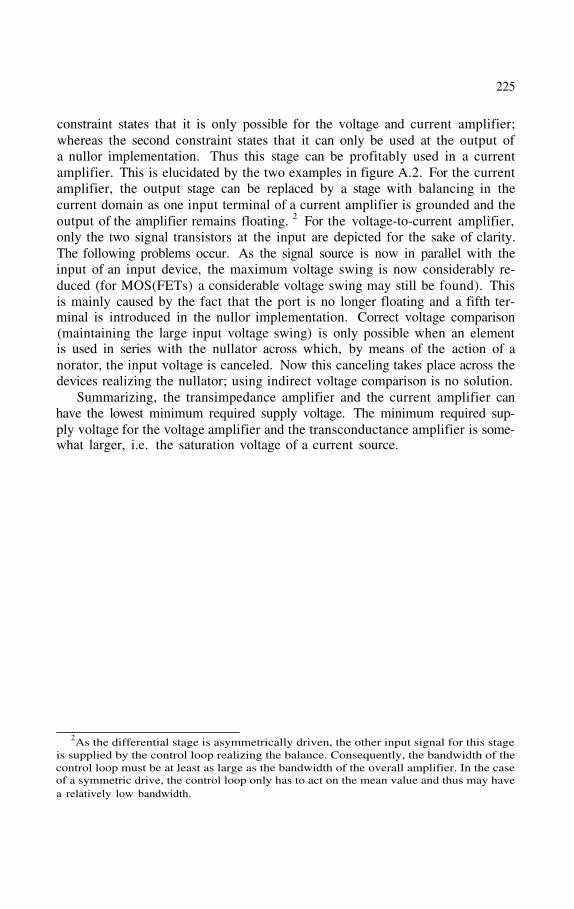
constraint states that it is only possible for the voltage and current amplifier;whereas the second constraint states that it can only be used at the output ofa nullor implementation. Thus this stage can be profitably used in a currentamplifier. This is elucidated by the two examples in figure A.2. For the currentamplifier, the output stage can be replaced by a stage with balancing in thecurrent domain as one input terminal of a current amplifier is grounded and theoutput of the amplifier remains floating. 2 For the voltage-to-current amplifier,only the two signal transistors at the input are depicted for the sake of clarity.The following problems occur. As the signal source is now in parallel with theinput of an input device, the maximum voltage swing is now considerably re-duced (for MOS(FETs) a considerable voltage swing may still be found). Thisis mainly caused by the fact that the port is no longer floating and a fifth ter-minal is introduced in the nullor implementation. Correct voltage comparison(maintaining the large input voltage swing) is only possible when an elementis used in series with the nullator across which, by means of the action of anorator, the input voltage is canceled. Now this canceling takes place across thedevices realizing the nullator; using indirect voltage comparison is no solution.
Summarizing, the transimpedance amplifier and the current amplifier canhave the lowest minimum required supply voltage. The minimum required sup-ply voltage for the voltage amplifier and the transconductance amplifier is some-what larger, i.e. the saturation voltage of a current source.
2As the differential stage is asymmetrically driven, the other input signal for this stageis supplied by the control loop realizing the balance. Consequently, the bandwidth of thecontrol loop must be at least as large as the bandwidth of the overall amplifier. In the caseof a symmetric drive, the control loop only has to act on the mean value and thus may havea relatively low bandwidth.
226 APPENDIX A. MINIMUM VOLTAGE FOR FEEDBACK AMPLIFIERS
Appendix B
Design example: class-ABamplifier
B.1 Introduction
A current trend in electronic design, is the design of low-voltage (1 V) low-powercircuits. These circuits have the advantage that they can be powered by
a single, relatively small battery; single as the supply voltage is only 1 V andrelatively small as the power consumption is low. The output amplifier presented[1] is a part of a completely-integrated single-chip 1 V LW receiver.
The effect of the low-voltage constraint (1 V) is mainly found in the circuitstopology. For high supply voltages, components and function blocks can bestacked between the supply rails; for a 1 V supply they need to be placed inparallel to meet the low-voltage specification [2].
The low-power constraint demands that the efficiency of a circuit must beas close to 100% as possible, and all the power from the power supply mustbe directed to the load. For a given supply voltage (without the use of chargepumping techniques, etc.) the low-power constraint becomes a low-current con-straint. All the current from the power supply must go through the load and allthe other currents must ideally be zero. This constraint has the largest influenceon those parts of the circuit where the signal currents are the largest. For in-stance, a small improvement in the efficiency of the output amplifier can resultin a reduction in current consumption equal to the total current consumptionof the input amplifier of the LW receiver.
Here the design of a highly efficient output amplifier for a 1 V supply isdescribed. Section B.2 describes the specifications and the choice of the basicconfiguration of the amplifier. In this section nullors [3] are used as the idealmodels for the active parts of the amplifier. The following sections discuss the
227
228 APPENDIX B. DESIGN EXAMPLE: CLASS-AB AMPLIFIER
implementation of the nullors. Section B.3 starts with some general commentson the implementation of the nullors. Section B.4 discusses the design of theoutput capability of the amplifier. In this section the focus is on the implemen-tation of the class-AB operation for power efficiency. The class-AB operation isrealized in the voltage domain and uses a version of the harmonic-mean relation.Subsequently, Section B.5 describes the behavior of the overall negative-feedbackloop, i.e. loop gain, poles and stability. This is followed by the implementationof the biasing circuitry and some final implementation details in Section B.6.Section B.7 describes the physical realization and the measurement results ofthe amplifier. Finally, the conclusions are given in Section B.8.
B.2 The basic structure of the output section
In the LW receiver the output section has two functions:
volume control
driving the earphone.
The input current for the complete output amplifier is leveled by an AGC to apeak value of approximately A signal current of about 1 mA results inan acceptable sound level [4]. To have some margin, the maximal peak outputcurrent is chosen to be 2.5 mA, resulting in a required maximum amplification of100. To be able to control the volume over a convenient range, the amplificationis chosen to be controllable between 10 and 100.
The block diagram of the amplifier is shown in figure B.1. The first amplifierblock has a variable gain between 1 and 10, whereas the second amplifier hasa fixed gain of 10. As the signal levels in the first amplifier are still relativelylow, the focus can be on the implementation of the variable gain instead of onthe power consumption. For the second amplifier, the power consumption is thekey item for optimization and this is not disturbed by the implementation of avariable gain. In this way the two functions, driving the load and controllingthe gain, are realized in separate amplifiers and can, consequently be optimizedindependently.
B.2. THE BASIC STRUCTURE OF THE OUTPUT SECTION 229
Here is dealt with the fixed-gain amplifier. The specifications for the ampli-fier are:
maximum input current
source impedance in parallel with 0.25 pF,
Load =
Gain = 10,
Bandwidth > 7 kHz,
Distortion < 1 %,
Supply voltage 1 to 1.5 V,
Supply current as low as possible,
Completely integrable in a bipolar process,
Temperature range -10°C to +40 °C.
A straightforward interpretation of these specifications leads to the choice ofa current amplifier. However, for a negative-feedback current amplifier, currentsensing has to be done at the output. The output stage of the amplifier must bebalanced, this can be done in the voltage or current domain [5], or the amplifiermust have indirect feedback [6]. For the sake of power efficiency, it is favorableto realize the amplifier in a class-AB fashion.
Realizing a balanced or indirect class-AB output stage is a tedious job.Therefore, a different type of amplifier has to be used. The load impedanceof the earphone is approximately and more or less constant over the fre-quency range of interest. Thus, the output of the amplifier may also be a voltage.In that case the feedback must sense the output voltage that is readily available.The final output current is determined by the impedance of the earphone. Theresulting amplifier is a transimpedance amplifier.
For a maximum current of 2.5 mA the voltage across the earphone is only75 mV. Grounding the earphone at one side results in saturation of one side ofthe AB output stage. Further, offset voltages at the output result in a relativelylarge offset current through the load as its impedance is only Therefore,the amplifier has to be realized completely balanced, see figure B.2. As bothamplifier halves are class AB, the signal current is comparable to that of thesingle-sided amplifier; only the quiescent current is doubled. Compared to thecurrent amplifier, the voltage amplifier is more power efficient as it does notrequire an additional current path for the current feedback.
In figure B.2 the gain blocks are nullors [3]. A nullor is an ideal elementwhich makes its input current and voltage zero by controlling its output current
230 APPENDIX B. DESIGN EXAMPLE: CLASS-AB AMPLIFIER
and voltage. In terms of gain parameters, the nullor has gain parameters whichare infinite. Therefore, the gain from input current to output voltage of thebalanced transimpedance amplifier is determined by the two feedback resistorsonly. To realize the required gain, the feedback resistors each have to be
B.3 Implementation of the nullors
Now the basic structure of the amplifier has been chosen, the implementationof the nullors is that remains. The implementation of nullors can be done inseveral more or less independent steps [7]. As the signals at the input of theamplifier are already relatively large, optimization with respect to noise is notnecessary. The remaining steps (condensed form) in chronological order are thedesign of:
Output capability,
Bandwidth and
Biasing.
These items are discussed in the following sections.
B.4 Output capability
The output capability of the amplifier is determined by the maximum outputsignal that can be supplied. As the load impedance is only the outputcapability is set by the maximum current which can be supplied. For thisamplifier this must be about 2.5 mA. For power-efficiency purposes the outputstage is chosen to be class AB. The current-gain factor of the transistors in the
B.4. OUTPUT CAPABILITY 231
DIMES01 process [8] are 80 for the PNP and 100 for the NPN. Consequently,the maximum input current of this stage amounts to When biasing thepreceding stage in class-A mode, the bias current needs to be in the order of 50
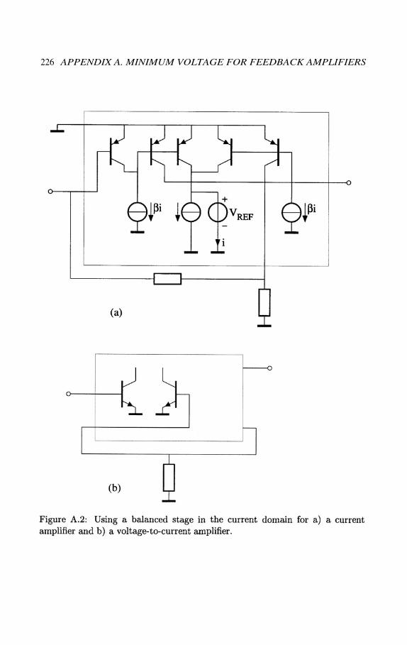
Therefore, this stage is also chosen to be class-AB. This is depicted in figureB.3. The voltage takes care of the class-AB operation [9]. The signs of thevoltage source correspond to the situation in which the supply voltage is 1 V, asthe sum of two base-emitters voltages is larger than 1 V. The implementationof this voltage source determines the final functioning of the AB control. Whenthis voltage source is just a fixed voltage the classical AB control is obtainedfor which the following holds:
Where and are the currents flowing through the two output transis-tors. When large output swings are required, the minimum current can be verylow, as the product of the two current is constant. Consequently, the of thecorresponding transistor may become too low, and an increase in distortion isfound. When the amplifier is used in a feedback structure, even oscillations mayoccur due to the switch-on delay of this transistor. Therefore, very often theharmonic-mean relation is used [10]:
When either or becomes very large, the other current is limited topreventing the corresponding transistor from becoming too slow.
232 APPENDIX B. DESIGN EXAMPLE: CLASS-AB AMPLIFIER
B.4.1 The voltage source for the class-AB control
The implementation of the voltage source, which takes care of the AB control,determines the final functioning of the AB operation. The conventional class-AB stage uses two series-connected diodes [11] 1. A reference current flowingthrough these two diodes determines the product of and Later on,other concepts were published that were able to work at supply voltages downto 1 V [9]. Here, however, the straightforward concept of [11] is extended tofunction for supply voltages down to 1 V. For these low supply voltages it is notpossible to use series-connected junctions. The generation of the control voltagehas to be done indirectly. The principle is depicted in figure B.4. The referencevoltage obtained for the class-AB control is given by:
with the supply voltage. Both and are determined byThis is accomplished by transistor and the nullor. The nullor
forces to flow completely through the collector of Transistoris in parallel with transistor and thus its collector current also
equals The nullor supplies the current through the resistor, at both sidesof the resistor, and thus the collector current of also has to be equal to
It must be noted that due to the low supply voltage, the voltage acrossthe resistor is of opposite polarity with respect to conventional AB stages.
By copying the current through the resistor to the current throughresistor the following relation is found:
1NB: traditionally two CC stages are used instead of two CE stages
233B.4. OUTPUT CAPABILITY
or by substitution of the expression for
This is just the expression for AB control. The influence of the supply voltage,as it is in the AB control voltage, cancels.
In this design is chosen to be As a result the quiescent currentof the first AB stage amounts to are four times as large as
The quiescent current of the second AB stage is approximatelyonly 1% of the maximum output current. The resistor is chosen to be
In that case the current through the resistor is in the order of the othercurrents in the reference source.
The implementation of the current copying from the reference source to theAB stage is discussed in paragraph B.4.3. The implementation of the nullor,which forces through the collector of is depicted in figure B.5.In principle, the nullor can be implemented by one CE stage [6]. However, asboth outputs of the nullor are required, an inverting and a non-inverting outputterminal must be realized. The two outputs of the CE stage, the collector andemitter, are not usable due to the low supply voltage. Using a differential pairfor implementing the nullor seems to be the next candidate [6]. However, inthat case two base-emitter junctions are in series for a NPN stage, which is notpossible for a 1 V supply, or the transistors are close to saturation in the case of
234 APPENDIX B. DESIGN EXAMPLE: CLASS-AB AMPLIFIER
a PNP stage. The combination of two parallel CE stages and a current mirrorfor the inversion leads to a convenient solution.
The output stages of the nullor implementation have to be biased as theymust be able to source and sink currents. For a 1.5 V supply the voltage across
is approximately +0.2 V (recalling the polarity convention of ). Whenthe battery is almost empty, the supply voltage is reduced to 1 V and the voltageacross is approximately -0.3 V. Therefore, the bias current is chosen tobe about to be able to cope with the complete range.
Frequency compensation of the loop comprising the nullor implementationand transistor is realized by pole splitting using pole-zero cancellation[7]. The closed loop exhibits a second-order Butterworth behavior with a band-width of approximately 1.4 MHz. The frequency compensation already took theinfluence of the current-copier implementations (to be discussed later on) intoaccount.
B.4.2 The ”harmonic-mean” control
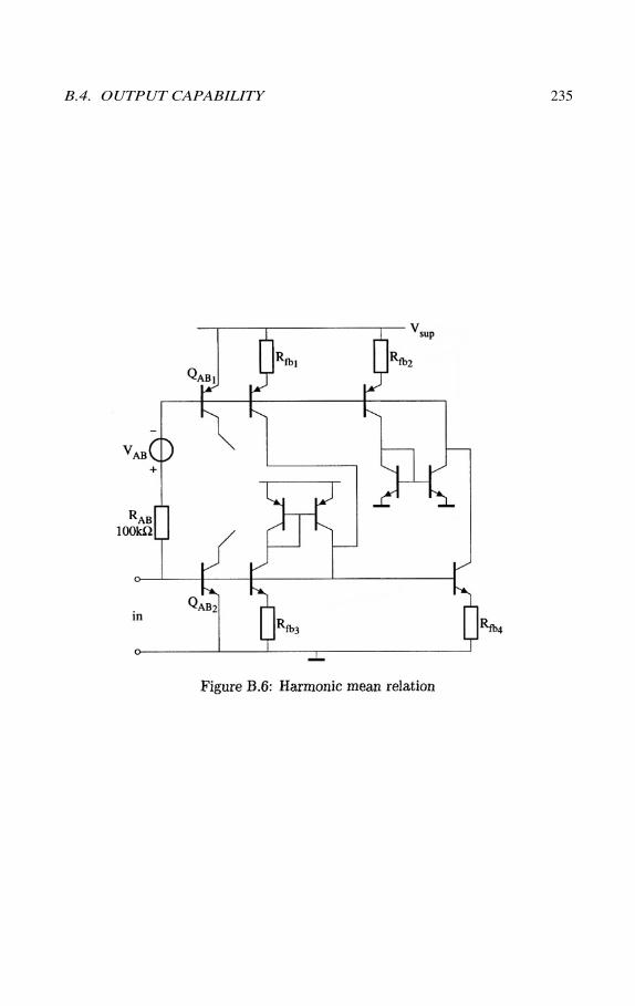
As already mentioned, using strict AB control has the disadvantage of havingtransistors with very low biasing currents and thus becoming slow. For ABstages that are not fed back, this results in an increase in distortion. For thisamplifier, which is fed back, the additional phase due to the switch-on delaycaused oscillations. Therefore, some control analogous to the harmonic-meanrelation has to be used. The product of the two transistor currents must notbe constant but has to increase for increasing output current (which is approxi-mately equal to the largest of both AB currents). The principal idea is depictedin figure B.6. In the figure only the first AB stage is depicted, andThe AB control voltage is modeled with a single voltage source and a resistor.
Two transconductance stages are placed in parallel to each AB transistor.Their transconductance is approximately equal to:
where is the feedback resistor of the transconductance stage and isthe transconductance of the transistor. Assume the current through be-comes relatively large; in that case the output current of its parallel-connectedtransconductance stages will also increase. The output current of the transcon-ductance is fed through the output of the AB-control-voltage source, resultingin a change of its voltage such that the base-emitter voltage of does notdecrease as much as it did originally. This results in a reduced decrease of itscollector current.
The current must be sunk at one side of the resistor and sourced at theother side of the resistor. If it was to be sourced or sunk at one side only, the
B.4. OUTPUT CAPABILITY 235
236 APPENDIX B. DESIGN EXAMPLE: CLASS-AB AMPLIFIER
input offset current of the complete AB stage, formerly only the base current,would change sign. Consequently, the overall loop gain of the amplifier wouldbecome positive when it was supposed to be negative. This sign reversal issignal dependent.
The harmonic-mean relation introduces a loop with a positive feedback. Thiscan be seen as follows. When one of the two AB currents becomes large, theproduct of the two currents is increased by the harmonic-mean relation. Thisincrease of the product can either cause an increase in the smallest AB current(this is the required option) or it can increase the current that is already large.Of course, a mix of both situations is also possible. When the large currentbecomes larger (the second option), the harmonic-mean relation increases theproduct even further and the current becomes even larger, and so on. Thispositive feedback loop must be counteracted by a stronger negative-feedbackloop. This loop must keep the output current of the complete stage undercontrol. Then the smallest AB current increases due to the harmonic-meanrelation.
To be certain, the loop gain of the positive loop can be kept below one. Theloop gain, T, of the positive loop shown in figure B.6 is approximately given by:
Now, with some straightforward reasoning, approximating expressions canbe found for the behavior of this AB control. The quiescent current of thefirst AB stage remains when it is assumed for the moment thatthe transconductance stages do not influence the AB control when it is in itsquiescent state. This assumption will be validated in a following paragraph.In the case of a relatively large signal excursion, the smallest current decreasesthe same factor as the largest current increases (for strict AB control) as theabsolute variations in base-emitter voltages of the two AB transistors are equal.However, for this version of harmonic-mean control, the absolute variation ofthe smallest base-emitter voltage can be approximated by:
The decrease in the smallest base-emitter voltage is reduced by Theresulting collector current can then be written as:
For T = 1, the variation of the smallest base-emitter voltage is zero (equationB.8) as the variation due to the largest base-emitter voltage is completely com-pensated. Thus, remains In figure B.7 a sketch is shown ofthe collector current of as a function of the input current, with the loopgain T as a parameter.
B.4. OUTPUT CAPABILITY 237
B.4.3 The current copiers
Now that the AB control has been implemented, attention can be paid to theimplementation of the current copiers. In figure B.8 the AB-control voltagesource is depicted again but now the current copiers are also drawn. The col-lector currents of transistor and minus the current from their biassources equals the current flowing through These copied currents flowthrough a resistor equal to and thus the voltage across is copiedand this copied voltage is allowed to float. In principle, the current flowing in orout at the other side of the resistor has to be copied from However, whenimplementing the rest of the output amplifier, this current source is in parallelwith the current source for the biasing of the first amplifying stage (see figureB.9, transistor and ), and does not need to be implemented explicitly.
Transistors and are required for the following reason. When theAB amplifier is in its quiescent state, some current already flows through thefour transconductance stages (see figure B.6). These currents result in an ad-
The expression for the loop gain of (B.7) holds when base currents and soon are ignored. However, due to the asymmetric drive of the amplifier, the basecurrent of flows through the output of the AB-control voltage source. Thiscurrent is in the opposite phase with respect to the current for the harmonic-mean control from the transconductance stages reducing their influence. Inorder to counteract this, the resistors in the transconductance stages at thePNP side are chosen to be at the NPN side these resistors are chosen tobe These resistors are somewhat smaller than as the of thetransistor reduces the complete transconductance, see (B.6).
238 APPENDIX B. DESIGN EXAMPLE: CLASS-AB AMPLIFIER
ditional voltage drop across of the AB-control voltage source, resulting ina quiescent current larger than This additional voltage drop canbe taken into account when calculating the quiescent current. However, thenthe relation between the quiescent current and is not very convenient. Itis better to compensate for this additional voltage drop. The collector currentof and are approximately equal to the sum of the quiescent currentsflowing through the NPN and the PNP transconductance stages, a scaling ofthree and a resistor of resulted in the desired behavior. This currentis used to cancel the quiescent current of the transconductance stages through
Now the quiescent current of the first AB stage is equal to again,except for the scaling factor of 0.25, of course.
B.5 The overall-loop behavior
The overall-loop behavior is determined by its dc loop gain, poles and zeros.When implementing the amplifier with only the two AB stages, the dc loopgain is very low. It is approximately:
where is the input resistance of either the NPN or PNP input stage, whichdepends on the polarity of the input signal. When
and the loop gain is approximately 0.01. This is, ofcourse, not practical and an additional amplifying stage has to be added. This
B.5. THE OVERALL-LOOP BEHAVIOR 239
stage adds gain to the loop as it is amplifying. Further, by choosing its biascurrent to be larger than as it is for the (quiescent) first AB stage, itsinput impedance reduces. Consequently, the fraction in expression (B.10) alsoincreases.
A convenient choice is a current mirror with a scaling factor of ten and abias current of the input transistor equal to One half of the amplifier isdepicted in figure B.9. For the sake of clarity, the harmonic-mean control isomitted in the figure. The loop gain increases due to the gain of the currentmirror by a factor of ten. Due to the lowered input impedance of the inputstage, the loop gain increases by an additional factor of about four hundred.Due to the output impedance of the current source at the output of the firststage the loop gain is reduced by a factor of 4. The resulting loop gain is about10. Frequency compensation is obtained by the pole-zero cancellation networksat the inputs of and Due to the varying bias current of the ABstages, the bandwidth of the amplifier varies as a function of the signal. At zerosignal the bandwidth is approximately 100 kHz, i.e. the poles are at 80 kHz ±60j kHz. For a large output signal (1.5 mA peak), the bandwidth is 2.2 MHzand poles are found at 1 MHz ± 2j MHz.
240 APPENDIX B. DESIGN EXAMPLE: CLASS-AB AMPLIFIER
B.6 The complete circuit
The complete circuit consists of two amplifier halves, one of which is depictedin figure B.9. To be able to drive a maximum current of about 2.5 mA to theload, the PNP output transistor is chosen to be twenty times as large asthe smallest PNP transistor in the DIMES01 technology (in order to prevent itfrom high-level injection at maximum output current). The maximum outputcurrent is limited by the saturation of the NPN output transistor Thecollector voltage of this transistor is more or less set by the base-emitter voltageof the input transistor, via the low-ohmic feedback resistor. This voltage isabout 0.58 V. When sinking an output current of several mA, the base-emittervoltage of becomes relatively large and the base-collector junction startsconducting. does not have this problem as its saturation currentis about 200 times as large as the saturation current of Thussaturates before saturates.
The quiescent current of the first AB stage is approximately which isslightly lower than the intended due to the influence of base-currents.The currents are bounded at the lower side to about For ideal transcon-ductance stages, the lower bound would have been as the loop gain wasdesigned to be 1. However, due to the signal dependency of the transconduc-tance, see equation B.6, the loop gain is for the relatively small signals smallerthan 1. For this application this poses no problems.
The biasing sources, depicted in the previous figures, are all derived fromone reference current by means of current copiers. For the measurements thiscurrent was supplied by an external source. Later on, when the complete receiverwill be integrated, a master reference source will be made.
B.7 Measurement results
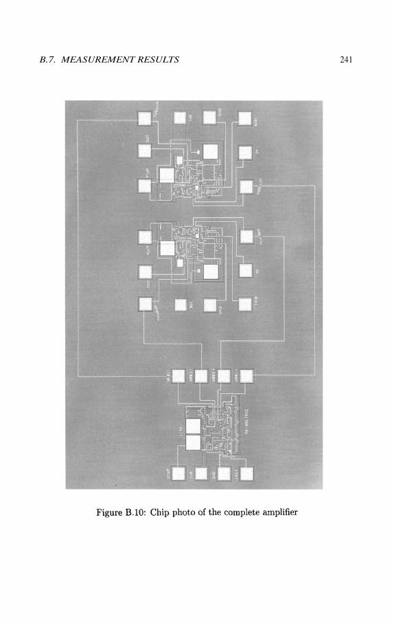
In figure B.10 a chip photo is depicted of the amplifier. The two large partsare the two amplifying halves and the smaller part is the circuit generating theAB-control voltage. When measurements were performed, the amplifier exhib-ited common-mode instability. The reason for this is that when the circuit isperforming normally, the load for each amplifier half is about However,when one half does not function properly, due to startup, for instance, its outputimpedance is not low and as a consequence, the load for the other amplifier halfbecomes very large. The loop gain of the amplifier half increases by a factorof 1000 due to this increase in the load impedance. When the complete am-plifier functions properly, the low load impedance reduces the loop gain by afactor of 1000. For normal operation, the amplifier was frequency-compensatedto a second-order behavior. However, due to the increase of loop gain, for thecommon-mode case, a third pole becomes important, driving the other two poles
B.7. MEASUREMENT RESULTS 241
242 APPENDIX B. DESIGN EXAMPLE: CLASS-AB AMPLIFIER
into the right half plane. For the measurements this problem was counteractedby connecting the middle of the load, via a large capacitor, to ground. Theload impedance for an amplifiers half is then determined independently of theother amplifier half. This large capacitor, however, cannot be used in the finalintegrated LW receiver. For that, a redesign has to be done using the principleas depicted in figure B.11. The two input stages, each comprising and(see figure B.9), are combined into one differential stage. The dotted drawn am-plifiers represent the AB stages. For common-mode signals the input impedanceof this stage is determined by the impedance of the tail-current source whichcan be rather high. For an Early voltage of 50 V, the impedance of both inputterminals to ground is about as only 1/22 part of the leakage currentthrough the impedance of the current source is seen At theoutput of the amplifier a relatively small capacitor will introduce a relativelylow-frequency pole, reducing the common-mode bandwidth. However, the in-put impedance to ground has a pole at a frequency equal to the frequency ofthe pole in the impedance of the current source. Thus, beyond this frequencythe common-mode loop gain increases (a zero). To be able to counteract theincrease of loop gain found by a factor of thousand, the pole at the output ofthe amplifier has to be a factor of a thousand lower than the pole in the current-source impedance. This can be done with relatively small capacitances (a fewpF). Of course, this low-frequency pole is not seen in the differential mode loop.The additional capacitor at the output only loads the much lower differentialmode impedance, shifting the corresponding pole a bit downwards, making areexamination of the frequency compensation necessary, of course.
In figure B.12 the spectrum of the output signal is depicted for an output
B.8. CONCLUSIONS AND DISCUSSION 243
signal at 1 kHz with an amplitude of 1 mA. The total harmonic distortion (usingthe harmonics up to 20 kHz), remains below to 0.9 %. This figure is more orless independent of the supply voltage. This figure was measured for a supplyvoltage of 1 V. Increasing the supply voltage to 1.5 V resulted in an improvementof some tenths of a dB.
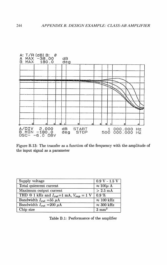
Figure B.13 depicts the transfer as a function of the frequency with theamplitude of the input signal as a parameter. The amplitude of the input signalwas logarithmically varied from to in steps of 4 dB. The bandwidthvaried from 100 kHz to 300 kHz. The bandwidth was lower than expected dueto the larger parasitics. The frequency compensation, however, proved to begood enough.
Finally, in table B.1 an overview of the measurement results is given.
B.8 Conclusions and discussion
In this appendix the design of a low-voltage low-power negative-feedback class-AB amplifier is described. The supply voltage can be as low as 0.9 V. The
244 APPENDIX B. DESIGN EXAMPLE: CLASS-AB AMPLIFIER
BIBLIOGRAPHY 245
quiescent current of the amplifier is only whereas the maximum outputcurrent is greater than 2.5 mA. The amplifier is capable of driving an earphonewith an impedance of The quiescent current of the output stage is only1% of the maximum output current.
This low quiescent current, relative to the maximum output current, is ob-tained by using class-AB biasing for the last two stages of the total of threestages. To prevent the transistors from becoming too slow, which is inherent instrict class-AB operation, a new type of implementation of the harmonic-meanrelation is described.
Due to the low-voltage constraint, the circuit for controlling the AB voltage,in order to obtain the harmonic-mean relation, is realized in an indirect way.This is necessary since it is not possible to stack conducting junctions betweenthe supply rails.
The chip showed a common-mode instability, which for this chip was solvedby grounding the middle of the load with a relatively large capacitor. Forthe final LW receiver, a balanced input stage is discussed which protects theamplifier from common-mode instability.
Bibliography[1] A. van Staveren, G.L.E. Monna, C.J.M. Verhoeven, and A.H.M. van Roer-
mund. A low-power class-ab negative feedback amplifier for a 1V LW re-ceiver. Analog Integrated Circuits and Signal Processing, 20:63–75, 1999.
[2] W.A. Serdijn. The Design of Low-Voltage Low-Power Analog IntegratedCircuits and Their Applications in Hearing Instruments. PhD thesis, DelftUniversity of Technology, February 1994.
[3] H.J. Carlin. Singular network elements. IEEE Transactions on CircuitTheory, 11:67–72, March 1964.
[4] M.P. Lubbers. An output amplifier for a 1 V portable AM receiver. Master’sthesis, Delft University of Technology, December 1994. In Dutch.
[5] A.C. van der Woerd and A.C. Pluygers. Biasing a differential pair in low-voltage analog circuits: A systematic approach. Analog Integrated Circuitsand Signal Processing, 3:119–125, 1993.
[6] E.H. Nordholt. The Design of High-Performance Negative-Feedback Am-plifiers. Elsevier, Amsterdam, 1983.
[7] C.J.M. Verhoeven, A. van Staveren, and G.L.E. Monna. Structured elec-tronic design, negative-feedback amplifiers. Lecture notes ET4 041, DelftUniversity of Technology, 1999. To appear at John Wiley & Sons LTD,Chichester.
246 APPENDIX B. DESIGN EXAMPLE: CLASS-AB AMPLIFIER
[8] L.K. Nanver, E.J.G. Goudena, and H.W. van Zeijl. DIMES-01, a baselineBIFET process for smart sensor experimentation. Sensors and Actuators,Part A, Physical, 36(2):139–149, April 1993.
[9] W.C.M. Renirie, K.J. de Langen, and J.H. Huijsing. Parallel feedforwardclass-AB control circuits for low-voltage low-power rail-to-rail output stagesof operational amplifiers. Analog Integrated Circuits and Signal Processing,8:37–48, 1995.
[10] E.Seevinck, W.de Jager, and P.Buitendijk. A low-distortion output stagewith improved stability for monolithic power amplifiers. IEEE Journal ofSolid-State Circuits, 23:794–801, June 1988.
[11] J.E. Solomon. The monolithic op amp: a tutorial study. IEEE Journal ofSolid-State Circuits, 9:314–332, December 1974.
Appendix C
The Effective Q versus thephase shift
In this appendix the effective Q of a resonator is calculated as a function of itsdetuning phase. The starting point is the impedance of the intrinsic resonator:
where s is the Laplace variable, and are the inductor, capacitor andresistor of the series resonator, respectively. The phase shift, as a function ofthe frequency, is given by:
The quality factor as a function of the frequency is defined as:
Applying this to equation (C.2) yields:
From equation (C.2) it follows that:
247
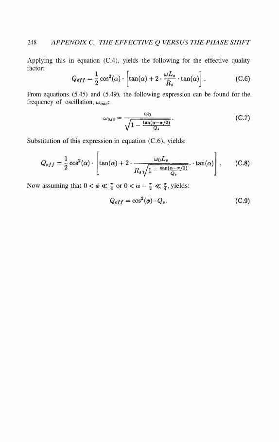
248 APPENDIX C. THE EFFECTIVE Q VERSUS THE PHASE SHIFT
Applying this in equation (C.4), yields the following for the effective qualityfactor:
From equations (5.45) and (5.49), the following expression can be found for thefrequency of oscillation,
Substitution of this expression in equation (C.6), yields:
Now assuming that or yields:
Appendix D
Design example:second-order compensatedBGR
D.1 Introduction
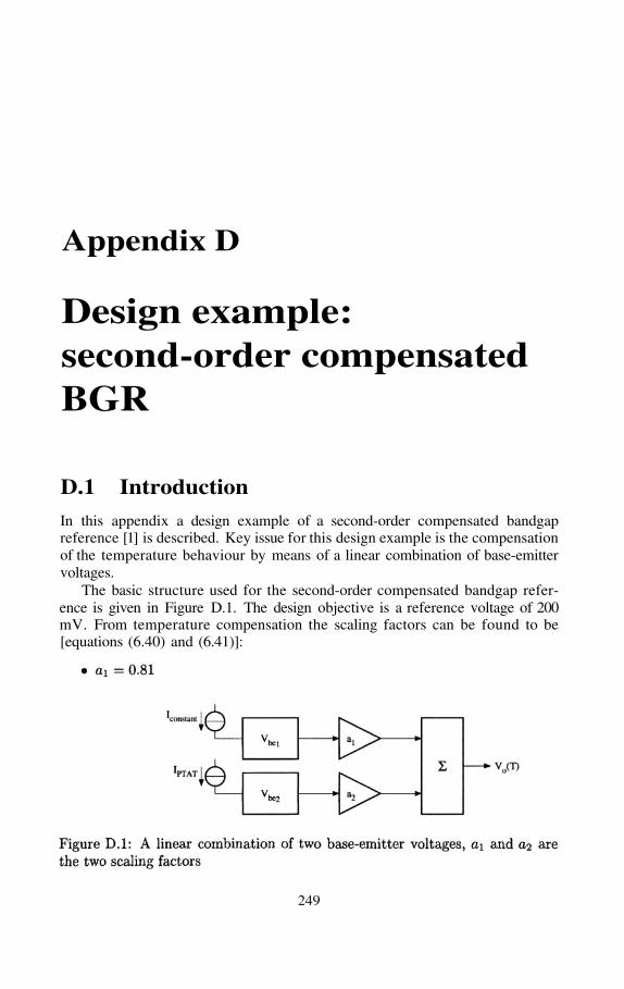
In this appendix a design example of a second-order compensated bandgapreference [1] is described. Key issue for this design example is the compensationof the temperature behaviour by means of a linear combination of base-emittervoltages.
The basic structure used for the second-order compensated bandgap refer-ence is given in Figure D.1. The design objective is a reference voltage of 200mV. From temperature compensation the scaling factors can be found to be[equations (6.40) and (6.41)]:
249
250 APPENDIX D. DESIGN EXAMPLE: 2nd ORDER BGR
For this design the following design parameters were used:
In the subsequent sections realistic implementations of the separate buildingblocks of figure D.1 are given. At the interface between two blocks, specialattention is paid to the possible interaction between the two blocks.
D.2 The design of the generatorIn chapter 6 is was shown that the relation between the base-emitter voltageand the collector current is important. Therefore, the collector current has tobe biased accurately. A bias circuit is needed that makes the collector currentequal to the desired value.
The base current of a transistor has a temperature dependency that is differ-ent than that of the collector current. Therefore, the base current is not allowedto have effect on the collector current. The bias circuit has to supply the basecurrent.
Further, the load current of the base-emitter voltage generator must notinfluence the collector bias current. The bias circuit has to supply the loadcurrent too.
Finally, to be able to ignore the forward Early effect, the bias circuit of thebase-emitter voltage generator has to make
The biasing of the transistor is depicted in Figure D.2. A nullor is usedfor the biasing circuit. A nullor is a two-port that regulates the input voltageand current to zero by regulating the output voltage and current (see also [2]).The input current of the nullor is zero so the bias current flows completelythrough the collector. The base and the load current are supplied by the nullor.Further, the input voltage of the nullor is zero, resulting in a zero base-collectorvoltage.
The next step in the design is to implement the nullor with a circuit. SeeFigure D.3.
For the input stage of the nullor implementation (a differential pair), MOStransistors are preferable because of the absence of input bias currents. However,the available process was a bipolar process so bipolar transistors had to be usedhere.
D.2. THE DESIGN OF THE GENERATOR 251
252 APPENDIX D. DESIGN EXAMPLE: 2nd ORDER BGR
with and the collector bias current of and it is indepen-dent of the noise contribution of the other transistors. Hence the bias currentof the input stage of the nullor implementation can be chosen to be very smallin order to obtain negligible input bias currents. Expression (D.1) assumes thatlow-noise current sources are available.
The value of the bias current of the output stage is based on the load andthe base current of
The available voltage for the tail current source of the differential pair isvery small. To obtain some extra voltage, the emitters of the transistors ofthe differential pair are enlarged. For each time the emitter area increases by afactor 10, 60mV is obtained. When MOS transistors with low threshold voltagesare available, the available voltage for the tail current source can be made largeenough without the need to enlarge transistors.
High-frequency stability is obtained by the pole-splitting networksand for the circuit generating . Because in the circuit gen-erating is biased at a different current than in the corresponding cir-cuit for (resulting in another pole-zero pattern), the pole-splitting network
has to be replaced by a pole-zero cancellation (the dotted network inFigure D.3).
D.3 The design of the combiner
The combiner scales and adds the two base-emitter voltages. The scaling of thebase-emitter voltages is realized passively. This passive scaling is implementedas a resistive divider and is shown in Figure D.4.
The scale factor equals:
The nullor is realized by a three-stage circuit for obtaining high loop gain.See Figure D.5. The high loop gain is necessary for reducing the non-linear
To minimize the influence of the input bias current and the load currenta second amplifying stage (a CE-stage) is used. To prevent the differential
pair from saturating at lower temperatures, an NPN is chosen for this secondstage.
To determine the optimum values of the bias currents, the equivalent noisevoltage at the output of the base-emitter voltage generator is examined. Theequivalent noise power density spectrum at the output of the
generator is approximately:
D.3. THE DESIGN OF THE COMBINER 253
offset voltage of the differential pair. This offset voltage is in series with the twoscaled base-emitter voltages and is caused by the current from the generatorfor flowing through the output stage of the combiner. To ease frequencycompensation for the third stage a current mirror with a scaling factor of 10 ischosen.
Because the divider is loaded now with an input bias current of the nullorimplementation (Figure D.5) a voltage equal to
is added to the output voltageFor the biasing currents the noise behavior is examined. All relevant noise
sources (Figure D.6) are transformed into an equivalent noise source atthe output with a power spectrum
with of the input transistors andTo minimize the noise power at the output, each part of the combiner circuit
should contribute less than the two base-emitter voltage generators contribute.This means that for the resistors of the dividers should hold:
254 APPENDIX D. DESIGN EXAMPLE: 2nd ORDER BGR
D.4. DESIGN OF THE BIAS CIRCUITS 255
and for the bias currents of the differential pair:
The output of the combiner is the output of the bandgap reference. There-fore the bandwidth of the output impedance of the combiner has to be as large aspossible. If this is the case, only a small capacitor in parallel with the output isneeded to obtain a low output impedance for the frequencies beyond that band-width. High-frequency stability is obtained by pole-zero cancellationand by resistive broadbanding . Although the resistive broadbanding re-duces the loop gain, this reduction of loop gain has no effect on the offset voltageof the differential pair because the resistive broadbanding is placed at the nodewhere the current from the generator is injected. The part of the currentcausing the offset voltage is decreased by the same factor as by which the loopgain is reduced.
D.4 Design of the bias circuits
One of the two base-emitter voltage generators has to be biased with a currentproportional to the absolute temperature, PTAT the other has to bebiased with a constant current (see for instance section 6.3.3.4). So,essentially, two types of bias currents have to be generated. All the other biascurrents can be derived from these two current sources.
D.4.1 The constant current source
The bias current with is easily derived from the output voltage via atransadmittance amplifier. However, this introduces a loop (Figure D.7).
To see if there is a unique DC solution for this loop the output voltage as afunction of the current I is calculated. The output voltage is given by:
with and Further the current I is given by
with the feedback resistor of the transadmittance amplifier. The graphicallydetermined solution of these two equations is shown in Figure D.8. It can beseen that there is only one DC solution.
256 APPENDIX D. DESIGN EXAMPLE: 2nd ORDER BGR
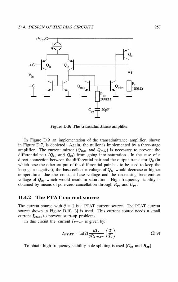
D.4. DESIGN OF THE BIAS CIRCUITS 257
In Figure D.9 an implementation of the transadmittance amplifier, shownin Figure D.7, is depicted. Again, the nullor is implemented by a three-stageamplifier. The current mirror is necessary to prevent thedifferential pair from going into saturation. In the case of adirect connection between the differential pair and the output transistor (inwhich case the other output of the differential pair has to be used to keep theloop gain negative), the base-collector voltage of would decrease at highertemperatures due the constant base voltage and the decreasing base-emittervoltage of which would result in saturation. High frequency stability isobtained by means of pole-zero cancellation through and
D.4.2 The PTAT current source
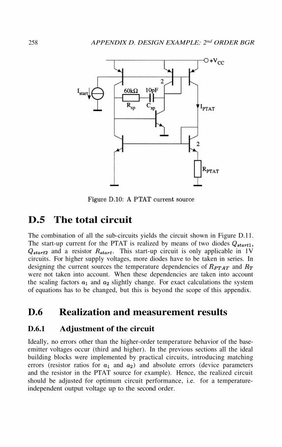
The current source with is a PTAT current source. The PTAT currentsource shown in Figure D.10 [3] is used. This current source needs a smallcurrent to prevent start-up problems.
In this circuit the current is given by:
To obtain high-frequency stability pole-splitting is used
258 APPENDIX D. DESIGN EXAMPLE: 2nd ORDER BGR
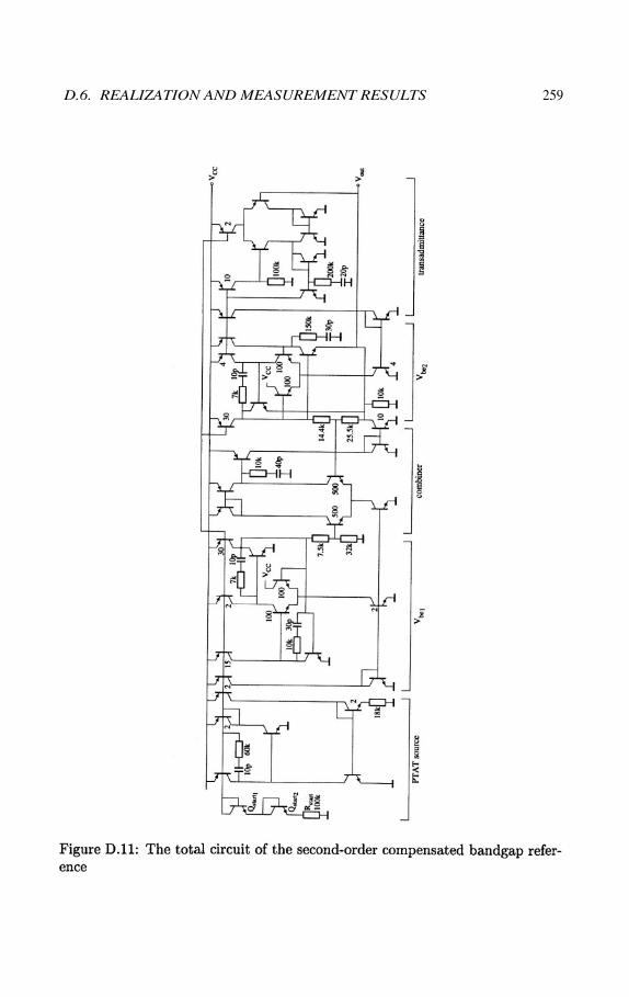
D.5 The total circuit
The combination of all the sub-circuits yields the circuit shown in Figure D.11.The start-up current for the PTAT is realized by means of two diodes
and a resistor This start-up circuit is only applicable in 1Vcircuits. For higher supply voltages, more diodes have to be taken in series. Indesigning the current sources the temperature dependencies of andwere not taken into account. When these dependencies are taken into accountthe scaling factors and slightly change. For exact calculations the systemof equations has to be changed, but this is beyond the scope of this appendix.
D.6 Realization and measurement results
D.6.1 Adjustment of the circuit
Ideally, no errors other than the higher-order temperature behavior of the base-emitter voltages occur (third and higher). In the previous sections all the idealbuilding blocks were implemented by practical circuits, introducing matchingerrors (resistor ratios for and ) and absolute errors (device parametersand the resistor in the PTAT source for example). Hence, the realized circuitshould be adjusted for optimum circuit performance, i.e. for a temperature-independent output voltage up to the second order.
D.6. REALIZATION AND MEASUREMENT RESULTS 259
260 APPENDIX D. DESIGN EXAMPLE: 2nd ORDER BGR
For the adjustment of the bandgap reference one resistor needs to be trimmed.This can be the resistor in the PTAT source or the resistor in thetransadmittance amplifier. These resistors determine the collector bias currentof the reference transistors and by that the constant and the first-order termof the base-emitter voltage. With this adjustment the first-order temperaturebehavior can be minimized. A constant error may remain after this adjustment.
In the case of too large matching errors between the resistors implement-ing the ratios and or too large absolute errors in or an additionaladjustment for minimizing the second-order behavior is necessary. This adjust-ment can be done by trimming one of the resistors of and and has to bedone before the first-order behavior is tuned because it affects the first-orderbehavior.
D.6.2 Realization
The circuit has been realized at the Delft Institute of Micro Electronics andSubmicron technology (DIMES) in the DIMES01 process withvertical NPNs and lateral PNPs. Typical parameters for the NPNs are:
and for the lateral PNPs: andThe capacitors are capacitors with a value of
For the frequency compensation of the generator the following valuesproved to be enough:For the pole-zero cancellation replacing a pole-splitting network in thegenerator, a resistor of and a capacitor of showed to be sufficient.For the combiner the pole-zero cancellation network is implemented by a resistorof and a capacitor of The resistive broadbanding is done by aresistor of Finally, the PTAT source and constant current source arestabilized by, respectively, with and with
The resistors for the scaling factors are for,respectively,
In Figure D.12 a photo of the chip is depicted. On this chip the resistorsare made controllable for testing purposes.
D.6.3 Measurement results
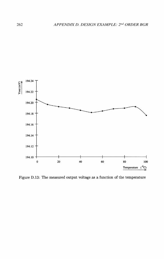
The measured output voltage as a function of temperature is depicted in FigureD.13. Other measurement results are summarized in table D.1.
From calculations on the idealized bandgap reference, a minimum tempera-ture dependency of 0.22 ppm/K can be found for the corresponding temperaturerange. This remaining dependency is a result of the non-compensated third andhigher-order temperature dependencies of the base-emitter voltage. However,to reach this, the influence of the remaining of the implementation must benegligibly small.
D.6. REALIZATION AND MEASUREMENT RESULTS 261
262 APPENDIX D. DESIGN EXAMPLE: 2nd ORDER BGR
D.6. REALIZATION AND MEASUREMENT RESULTS 263
The main causes for the deviation of the realized bandgap reference fromthis number are twofold. First, for the lower temperatures the voltage availablefor the tail-current source of the differential pair in the summator becomes toolow. Consequently, saturation of this source occurs, and as the differential pairis not used completely symmetrically, errors are found in the reference voltage.Note that the 1.5 ppm/K over the complete temperature range of this bandgapreference is equivalent to a total deviation of only 30 see figure D.13. Thisbehavior can be improved by enlarging the voltage drop across the current sourceor by choosing summation in the current domain; the differential pair and thecurrent source can then even be removed. The current sources supplying thecurrents for the two reference transistors do not introduce errors as their voltageis at least about 250 mV at 0 °C and thus the errors are negligible, see section6.7.2.3.
Second, at the higher end of the temperature range, the deviation is mainlycaused by the influence of leakage currents. At about 125 °C a sharp drop in thereference voltage was found (on the order of several mV over a range of 10 °C),which influence is already noticeable at 100 °C, see figure D.13. For improvingthe bandgap reference in this region, the leakage currents and their temperaturebehavior have to be taken into account. In [4] a thorough treatment of thecurrents in the bipolar transistor can be found, including saturation currents(i.e. the leakage currents of PN-junctions).
This bandgap reference was specially designed to verify the feasibility of atemperature compensation by means of a linear combination of base-emittervoltages. At the time of the design, the the noise production of second-ordercompensated bandgap references was not yet studied in detail. For the biascurrent of the two reference transistors a large ratio was chosen as this wasthought to be a correct choice. The total equivalent noise production of theidealized bandgap reference (sealer, adder and biasing still ideal) amounts toabout 20 One reference transistor was biased at whereas theother was biased at . However, later on from noise minimization wasfound, see section 6.5.1.2, that for optimum noise performance the current ratio
264 APPENDIX D. DESIGN EXAMPLE: 2nd ORDER BGR
of these two currents should be the same as the ratio of the two scaling factors(which equals about 0.8 and differs considerably from the used collector cur-rent ratio). When the optimum ratio for the collector currents is used, equation(6.65) applies and the minimum noise level for a current consumption ofis found to be about a factor 4 better. As the noise contributionof the biasing is a relative contribution, the expected noise of the complete opti-mized bandgap reference, for the same power consumption is about(from table F.1 a ratio of 4 is found between the noise of the idealized bandgapreference and the noise of the idealized bandgap reference). This is a factor 4lower compared with the noise production of the realized reference!
D.7 Conclusion
In this appendix the design of a 1-V second-order compensated bandgap refer-ence circuit has been presented. Only two base-emitter voltages are needed toobtain compensation up to the second order. One of the transistors is biasedwith a PTAT current and the other is biased with a constant current. Therealized circuit has an output voltage of approximately 194mV and the meantemperature dependency is 1.5 ppm/°C in the range of 0°C to 100°C. The cir-cuit has been realized in a bipolar process with The total amountof capacitance is approximately 150pF and the current consumption is about
Bibliography
A. van Staveren, J. van Velzen, C.J.M. Verhoeven, and A.H.M. van Roer-mund. An integratable second-order compensated bandgap reference for 1Vsupply. Analog Integrated Circuits and Signal Processing, 8:69–81, 1995.
H.C. Nauta and E.H. Nordholt. New class of high-performance ptat currentsources. Electronics Letters, 21(9):384–386, April 1985.
K. v.d. Lingen. Bipolar Transistors for usage in Monolithic Bandgap Refer-ences and Temperature Transducers. PhD thesis, Delft University of Tech-nology, Delft, 1996.
[1]
[2]
[3]
[4]
Appendix E
Optimum ratio ofsaturation currents
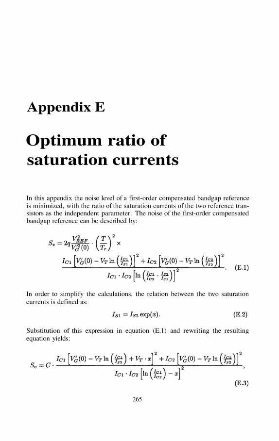
In this appendix the noise level of a first-order compensated bandgap referenceis minimized, with the ratio of the saturation currents of the two reference tran-sistors as the independent parameter. The noise of the first-order compensatedbandgap reference can be described by:
In order to simplify the calculations, the relation between the two saturationcurrents is defined as:
Substitution of this expression in equation (E.1) and rewriting the resultingequation yields:
265
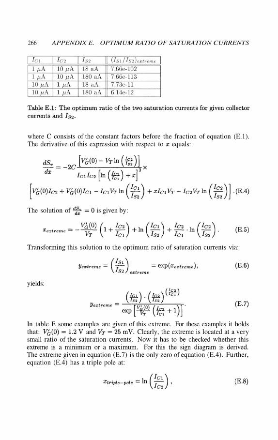
266 APPENDIX E. OPTIMUM RATIO OF SATURATION CURRENTS
where C consists of the constant factors before the fraction of equation (E.1).The derivative of this expression with respect to equals:
The solution of is given by:
Transforming this solution to the optimum ratio of saturation currents via:
yields:
In table E some examples are given of this extreme. For these examples it holdsthat: and Clearly, the extreme is located at a verysmall ratio of the saturation currents. Now it has to be checked whether thisextreme is a minimum or a maximum. For this the sign diagram is derived.The extreme given in equation (E.7) is the only zero of equation (E.4). Further,equation (E.4) has a triple pole at:
267
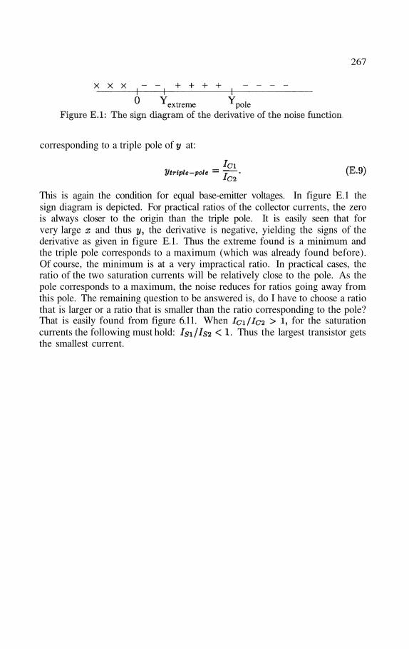
corresponding to a triple pole of at:
This is again the condition for equal base-emitter voltages. In figure E.1 thesign diagram is depicted. For practical ratios of the collector currents, the zerois always closer to the origin than the triple pole. It is easily seen that forvery large and thus the derivative is negative, yielding the signs of thederivative as given in figure E.1. Thus the extreme found is a minimum andthe triple pole corresponds to a maximum (which was already found before).Of course, the minimum is at a very impractical ratio. In practical cases, theratio of the two saturation currents will be relatively close to the pole. As thepole corresponds to a maximum, the noise reduces for ratios going away fromthis pole. The remaining question to be answered is, do I have to choose a ratiothat is larger or a ratio that is smaller than the ratio corresponding to the pole?That is easily found from figure 6.11. When for the saturationcurrents the following must hold: . Thus the largest transistor getsthe smallest current.
Appendix F
Design example: first-ordercompensated BGR
F.1 Introduction
In section 6.5.1.1 the noise behavior of an idealized bandgap reference wastreated. In this appendix a design example of a practical low-noise bandgapreference [1] is described to determine which parts of the implementation con-tribute in what extent in addition to the noise, so that the fundamental limit isnot reached.
First attention is paid to the basic structure of the bandgap reference andsubsequently the constituting blocks are implemented one by one. Via simula-tions the noise performance is verified.
F.2 The basic structure of the design example
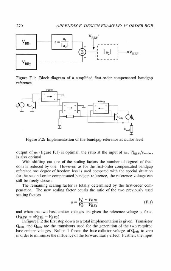
For this design example a simplified structure is used. This structure is obtainedby shifting one scaling factor out of the bandgap reference (cf. section 6.8). Infigure F.1 the block diagram of the example bandgap reference is given. Theblock diagram is found from figure 6.7 by shifting sealer through the summingnode and subsequently deleting this sealer at the output. As the sealer istemperature independent the newly created reference voltage is also temperatureindependent . Here it is assumed that sealer is negativeand is positive. Thus the summing node has to subtract from thescaled . For this block diagram the noise optimization of the previoussections still holds. Scaler does not contribute any noise in the optimization.So, when the ratio of the reference voltage and the noise voltage at the
269
270 APPENDIX F. DESIGN EXAMPLE: 1st ORDER BGR
output of (figure F.1) is optimal, the ratio at the input ofis also optimal.
With shifting out one of the scaling factors the number of degrees of free-dom is reduced by one. However, as for the first-order compensated bandgapreference one degree of freedom less is used compared with the special situationfor the second-order compensated bandgap reference, the reference voltage canstill be freely chosen.
The remaining scaling factor is totally determined by the first-order com-pensation. The new scaling factor equals the ratio of the two previously usedscaling factors
and when the two base-emitter voltages are given the reference voltage is fixed
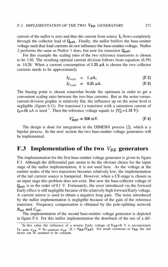
In figure F.2 the first step down to a total implementation is given. Transistorand are the transistors used for the generation of the two required
base-emitter voltages. Nullor 1 forces the base-collector voltage of to zeroin order to minimize the influence of the forward Early effect. Further, the input
F.3. IMPLEMENTATION OF THE TWO GENERATORS 271
current of the nullor is zero and thus the current from source flows completelythrough the collector lead of . Finally, the nullor buffers the base-emittervoltage such that load currents do not influence the base-emitter voltage. Nullor2 performs the same as Nullor 1 does, but now for transistor
For this example the scaling ratio of the two reference transistors is chosento be 1:10. The resulting optimal current division follows from equation (6.59)as 1:0.28. When a current consumption of is chosen the two collectorcurrents needs to be approximately
F.3 Implementation of the two generators
The implementation for the first base-emitter voltage generator is given in figureF.3. Although the differential pair seems to be the obvious choice for the inputstage of the nullor implementation, it is not used here. As the voltage at theemitter nodes of the two transistors becomes relatively low, the implementationof the tail current source is hampered. However, when a CE-stage is chosen asan input stage this problem does not exist. But now the base-collector voltage of
is in the order of 0.1 V. Fortunately, the error introduced via the forwardEarly effect is still negligible because of the relatively high forward Early voltage.A current mirror is used to obtain a negative loop gain. The noise introducedby the nullor implementation is negligible because of the gain of the referencetransistor. Frequency compensation is obtained by the pole-splitting network
The implementation of the second base-emitter voltage generator is depictedin figure F.4. For this nullor implementation the drawback of the use of a dif-
1In this value the influence of a reverse Early voltage of V is incorporated.For small variations in the last
factor can be assumed to be constant.
The design is done for integration in the DIMES01 process [2], which is abipolar process. In the next section the two base-emitter voltage generators willbe implemented.
The biasing point is chosen somewhat beside the optimum in order to get aconvenient scaling ratio between the two bias currents. But as the noise-versus-current-division graphic is relatively flat, the influence up on the noise level isnegligible (figure 6.11). For transistor 1 a transistor with a saturation current of
aA is used 1. Then the reference voltage equals to
.
272 APPENDIX F. DESIGN EXAMPLE: 1st ORDER BGR
F.4. THE IMPLEMENTATION OF THE SCALER 273
ferential pair as input stage is not apparent because the common-mode voltageof this nullor is 200mV higher than it is for nullor 1. As the differential pair hasa non-inverting output, no additional stage is needed to obtain a negative loopgain. Without additional frequency compensation components the circuit al-ready showed an acceptable frequency behavior. As for the generator, thenoise is predominantly determined by the collector shot noise of the referencetransistor.
At this point of the design the total noise power density of the (idealized)bandgap reference equals:
with . In the next section an implementation shall be made for thescaler.
F.4 The implementation of the scaler
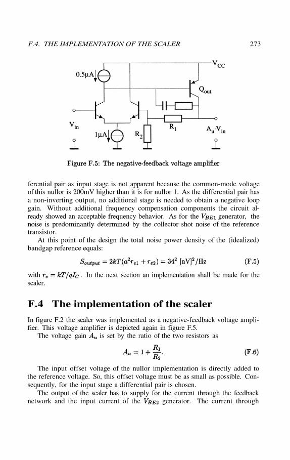
In figure F.2 the scaler was implemented as a negative-feedback voltage ampli-fier. This voltage amplifier is depicted again in figure F.5.
The voltage gain is set by the ratio of the two resistors as
The input offset voltage of the nullor implementation is directly added tothe reference voltage. So, this offset voltage must be as small as possible. Con-sequently, for the input stage a differential pair is chosen.
The output of the scaler has to supply for the current through the feedbacknetwork and the input current of the generator. The current through
274 APPENDIX F. DESIGN EXAMPLE: 1st ORDER BGR
the feedback network is related to and thus temperature dependent. Theinput current of the generator equals its load current, as the generatoracts as a floating voltage source, plus an input offset current. This input offsetcurrent is also temperature dependent. Thus the total load current of the scaleris temperature dependent. Transistor is used to supply this load currentand to reduce the influence of this current on the input offset voltage.
The equivalent input noise power density of the scaler equals
The first term is due to the thermal noise of the feedback network and the equiv-alent voltage noise of the input stage. The second term is due to the equivalentnoise current of the input stage. A minimum exists for the noise contributionof the input stage. For increasing collector current the equivalent voltage noiseof the input stage decreases, but the influence of the equivalent current noiseincreases, and vice versa for a decreasing collector current. Thus a minimumis obtained when for a small change in collector current the change in equiva-lent noise voltage of the input stage is compensated for by the complementarychange of the equivalent input noise current. As the influence of the input noisecurrent is dependent on the feedback resistors, this minimum is too.
For the noise due to the feedback resistors it holds that the lower the resistorvalues are, the less the noise contribution is. But as the voltages across thoseresistors are determined by the base-emitter voltages, the current consumptionis directly related to their noise performance. For a lower noise contribution ahigher current consumption is required.
For the current consumption of the resistors as a function of the base-emittervoltages it holds that
in which is the current through the feedback network. The influence of theequivalent input noise voltage of the scaler on the noise at the output of thereference is found by multiplying by the scaling factor a. As the scaling factoris given by
and the practical base-emitter voltages are limited to a relatively small range,the factor is more or less independent of the base-emitter voltages.
Concluding, the noise contribution due to the feedback resistors can onlybe reduced, reasonably, by increasing the current consumption. A compromisehas to made between the current consumption and noise contribution. For thefeedback resistors the following values are chosen
F.5. THE COMPLETE CIRCUIT 275
Resistors of this value are readily available in current technologies. Becausethe resistors set an amplification factor, only the matching is important. Forthese resistors the current consumption is approximately equal to the currentconsumption of the two reference transistors. The noise contribution is of thesame order.
Now that the feedback resistors are known, a noise minimization for theinput stage can be performed. Doing so, an optimal collector current of 3.5
for each transistor of the input stage is found. In that case the equivalentnoise resistor of the input stage amounts to which is negligible. Butthe current consumption is relatively high and thus a lower collector currentis chosen: for each input transistor. Now the equivalent noise resistorequals and the noise contribution is of the order of the noise due to the
generator.The high-frequency behavior of the sealer is compensated by a pole-splitting
network.
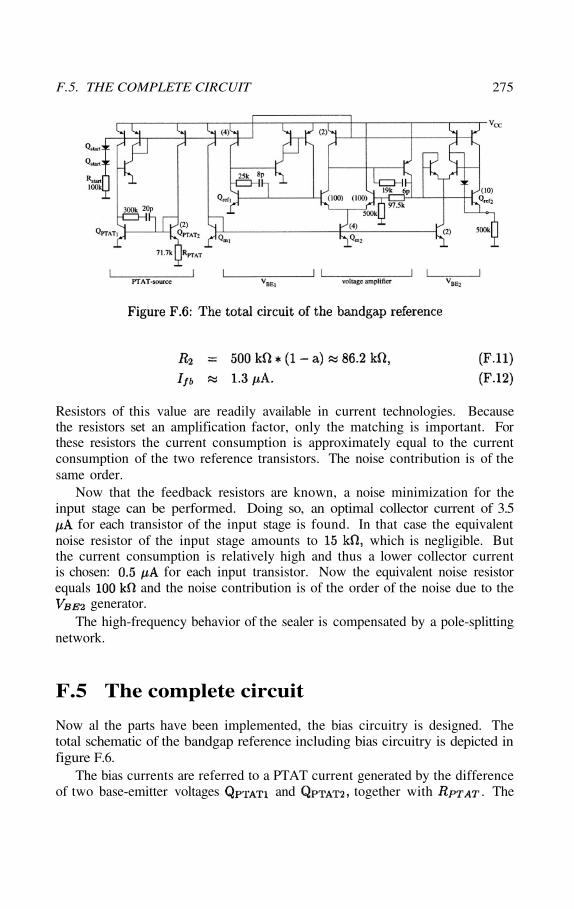
F.5 The complete circuit
Now al the parts have been implemented, the bias circuitry is designed. Thetotal schematic of the bandgap reference including bias circuitry is depicted infigure F.6.
The bias currents are referred to a PTAT current generated by the differenceof two base-emitter voltages and together with . The
276 APPENDIX F. DESIGN EXAMPLE: 1st ORDER BGR
noise contribution of this part to the noise of the bias currents is given by
To realize a negligible contribution to the noise, the currents in the PTATsource need to be relatively large and a large differencein the base-emitter voltage is needed in order to be able to use a high valuefor . In contrast, the noise due to the current mirrors on the top of thePTAT source and the transistors implementing the current bias sources can notbe made negligible because of the power supply voltage of only 1 V. For thisdesign example the 1 V power supply voltage is a constraint. Thus lowering theinfluence of the noise of the PTAT current source must be done by increasingits current consumption.
As a compromise between current consumption and noise contribution, thefollowing values are used for the PTAT source
Startup is secured by the two diodes and a resistorA simulation result of the temperature behavior of the total bandgap refer-
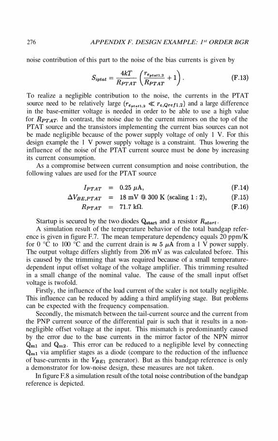
ence is given in figure F.7. The mean temperature dependency equals 20 ppm/Kfor 0 °C to 100 °C and the current drain is from a 1 V power supply.The output voltage differs slightly from 206 mV as was calculated before. Thisis caused by the trimming that was required because of a small temperature-dependent input offset voltage of the voltage amplifier. This trimming resultedin a small change of the nominal value. The cause of the small input offsetvoltage is twofold.
Firstly, the influence of the load current of the scaler is not totally negligible.This influence can be reduced by adding a third amplifying stage. But problemscan be expected with the frequency compensation.
Secondly, the mismatch between the tail-current source and the current fromthe PNP current source of the differential pair is such that it results in a non-negligible offset voltage at the input. This mismatch is predominantly causedby the error due to the base currents in the mirror factor of the NPN mirror
and . This error can be reduced to a negligible level by connectingvia amplifier stages as a diode (compare to the reduction of the influence
of base-currents in the generator). But as this bandgap reference is onlya demonstrator for low-noise design, these measures are not taken.
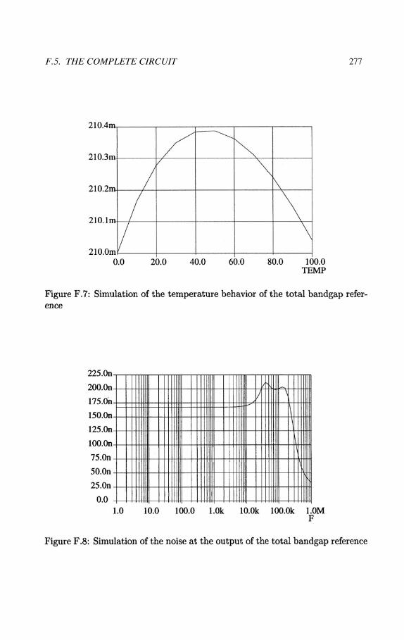
In figure F.8 a simulation result of the total noise contribution of the bandgapreference is depicted.
.
F.5. THE COMPLETE CIRCUIT 277
278 APPENDIX F. DESIGN EXAMPLE: 1st ORDER BGR
The total noise amounts to approximately . The contributionsof the different parts of the bandgap reference are given in table F.1
Note that the noise contribution of the biasing circuit is relatively large.This is inherent in low-voltage design (in this case 1 V). All the transistors usedfor the biasing contribute at least noise to the bias currents and the PTATcurrent source makes an additional contribution to the noise. Noise contributioncan be minimized when emitter resistors are used. With the emitter resistors,the noise contribution can be reduced to . However, to reach this, relativelylarge resistors and thus a relatively high voltage for a given current, is needed.It can be calculated fairly simple that in order to obtain a noise contribution of
, which is still negligible, the voltage across the emitter resistors needs tobe approximately 5 V. A closer look shows that a considerable reduction of thenoise contribution is already obtained for about 100 mV across the resistors.Then the noise power of the biasing can be reduced to about 5 % of the originallevel, see equation (6.78).
Thus one can say that the performance versus power consumption of bandgapreferences is not degraded that much by the 1 V power supply constraint. For1 V design, the influence of the bias sources on the noise behavior can be ac-counted for by just a factor. Of course this factor depends on how the biascircuit is designed.
The bias circuit not only contributes to the noise by its own shot noise.Noise from the power supply penetrates through the practical bias sources tothe output of the bandgap reference and contributes to the noise as well. Thesensitivity of the bandgap reference to power supply noise is determined by theimplementation for the bias sources (how much noise is injected) and the transferof the injected noise to the output (what is seen of the injected noise). Atrelatively high frequencies in particular it is hard to make a good implementationof the bias sources such that the injected noise is kept low. When the injectednoise is predominant at high frequencies, additional measures in the bandgapreference circuit have to be taken such that noise injected at different nodescancel at the output of the bandgap reference or are attenuated in the bandgapreference. These measures can be done independently of the noise optimization.
F.6. CONCLUSIONS 279
Besides the noise contribution due to the bias circuit, the noise of the scalerprevents the bandgap reference from reaching the fundamental limit. As waspointed out, more current through the feedback resistors and input stage reducesthe noise contribution of the scaler. But the noise of the idealized bandgapreference (the two base-emitter voltage generators) also decreases when largercurrents are used. Thus in the division of the total current between the twobase-emitter voltage generators and the scaler there is an optimum at which thetotal noise level is minimal. The noise optimization described by the strategyin this appendix will not be far from this global optimum. This is becausethe noise performance of the scaler is only slightly influenced by the valuesof the base-emitter voltages of the reference transistors [via the scaling factorequation (F.1)]. Thus when noise of the two base-emitter voltages and the scalerare minimized separately and their levels are comparable, the total noise levelwill be close to the global optimum.
F.6 ConclusionsIn this appendix a design example was shown of a special structure of a first-order compensated bandgap reference. For this design noise minimization wasthe key issue, i.e. how close can the noise level be to the noise level of theidealized bandgap reference.
For this example it was found that the noise contribution of the voltageamplifier, implementing the single scaling factor, is easily made on the sameorder of magnitude as the noise contribution of the idealized bandgap reference.On top of that it was shown that the noise contribution due to the biasingcircuitry is easily made small compared with the noise of the rest of the reference.
The designed bipolar bandgap reference has an output voltage of about200 mV and the mean temperature dependency is for 0 °C to100 °C (which is a direct consequence of the first-order temperature compen-sation). The output noise density equals The total currentconsumption is
Bibliography
A. van Staveren, C.J.M. Verhoeven, and A.H.M. van Roermund. The designof low-noise bandgap references. IEEE Transactions on Circuits and SystemsI, 43(4):290–300, April 1996.
L.K. Nanver, E.J.G. Goudena, and H.W. van Zeijl. DIMES-01, a baselineBIFET process for smart sensor experimentation. Sensors and ActuatorsPhysical, 36(2):139–147, 1993.
[1]
[2]
Index
A( ), 31A( ) ( ), 31
3131
11631
1/f noise, 181
accurate circuit design, 29active part transfer, 31amplifier, 2, 37, 39, 76
bandwidth, 84dedicated, 75design example, 227distortion, 78general purpose, 75noise, 77