97
USER GUIDE mITX-SKL-H Doc. Rev.0.3 Preliminary Doc. ID: 1060-7483

USER GUIDE
mITX-SKL-H Doc. Rev.0.3 Preliminary
Doc. ID: 1060-7483

mITX-SKL-H – Doc. Rev.0.3 Preliminary
www.kontron.com // 2
MITX-SKL-H - USER GUIDE
Disclaimer Kontron would like to point out that the information contained in this user guide may be subject to alteration, particularly as a result of the constant upgrading of Kontron products. This document does not entail any guarantee on the part of Kontron with respect to technical processes described in the user guide or any product characteristics set out in the user guide. Kontron assumes no responsibility or liability for the use of the described product(s), conveys no license or title under any patent, copyright or mask work rights to these products and makes no representations or warranties that these products are free from patent, copyright or mask work right infringement unless otherwise specified. Applications that are described in this user guide are for illustration purposes only. Kontron makes no representation or warranty that such application will be suitable for the specified use without further testing or modification. Kontron expressly informs the user that this user guide only contains a general description of processes and instructions which may not be applicable in every individual case. In cases of doubt, please contact Kontron.
This user guide is protected by copyright. All rights are reserved by Kontron. No part of this document may be reproduced, transmitted, transcribed, stored in a retrieval system, or translated into any language or computer language, in any form or by any means (electronic, mechanical, photocopying, recording, or otherwise), without the express written permission of Kontron. Kontron points out that the information contained in this user guide is constantly being updated in line with the technical alterations and improvements made by Kontron to the products and thus this user guide only reflects the technical status of the products by Kontron at the time of publishing.
Brand and product names are trademarks or registered trademarks of their respective owners.
© 2013, 2014 by Kontron America, ©2016 by Kontron AG
Kontron AG
Lise-Meitner-Str. 3-5 86156 Augsburg Germany www.kontron.com

mITX-SKL-H – Doc. Rev.0.3 Preliminary
www.kontron.com // 3
High Risk Applications Hazard Notice THIS DEVICE AND ASSOCIATED SOFTWARE ARE NOT DESIGNED, MANUFACTURED OR INTENDED FOR USE OR RESALE FOR THE OPERATION OF NUCLEAR FACILITIES, THE NAVIGATION, CONTROL OR COMMUNICATION SYSTEMS FOR AIRCRAFT OR OTHER TRANSPORTATION, AIR TRAFFIC CONTROL, LIFE SUPPORT OR LIFE SUSTAINING APPLICATIONS, WEAPONS SYSTEMS, OR ANY OTHER APPLICATION IN A HAZARDOUS ENVIRONMENT, OR REQUIRING FAIL-SAFE PERFORMANCE, OR IN WHICH THE FAILURE OF PRODUCTS COULD LEAD DIRECTLY TO DEATH, PERSONAL INJURY, OR SEVERE PHYSICAL OR ENVIRONMENTAL DAMAGE (COLLECTIVELY, "HIGH RISK APPLICATIONS").
You understand and agree that your use of Kontron devices as a component in High Risk Applications is entirely at your risk. To minimize the risks associated with your products and applications, you should provide adequate design and operating safeguards. You are solely responsible for compliance with all legal, regulatory, safety, and security related requirements concerning your products. You are responsible to ensure that your systems (and any Kontron hardware or software components incorporated in your systems) meet all applicable requirements. Unless otherwise stated in the product documentation, the Kontron device is not provided with error-tolerance capabilities and cannot therefore be deemed as being engineered, manufactured or setup to be compliant for implementation or for resale as device in High Risk Applications. All application and safety related information in this document (including application descriptions, suggested safety measures, suggested Kontron products, and other materials) is provided for reference only.

mITX-SKL-H – Doc. Rev.0.3 Preliminary
www.kontron.com // 4
Revision History Revision Brief description of changes Date of issue
0.1 Preliminary version 2016-Sept-20
0.2 Preliminary version- Added BIOS Setup Menu 2016-Oct-07
0.3 Updated the BIOS setup menus Added Power +12 V to +24 V DC information Changed board figures
2016-Dec-05
Terms and Conditions Kontron warrants products in accordance with defined regional warranty periods. For more information about warranty compliance and conformity, and the warranty period in your region, visit http://www.kontron.com/terms-and-conditions.
Kontron sells products worldwide and declares regional General Terms & Conditions of Sale, and Purchase Order Terms & Conditions. Visit http://www.kontron.com/terms-and-conditions.
For contact information, refer to the corporate offices contact information on the last page of this user guide or visit our website CONTACT US.
Customer Support Find Kontron contacts by visiting: http://www.kontron.com/support.
Customer Service As a trusted technology innovator and global solutions provider, Kontron extends its embedded market strengths into a services portfolio allowing companies to break the barriers of traditional product lifecycles. Proven product expertise coupled with collaborative and highly-experienced support enables Kontron to provide exceptional peace of mind to build and maintain successful products.
For more details on Kontron’s service offerings such as: enhanced repair services, extended warranty, Kontron training academy, and more visit http://www.kontron.com/support-and-services/services.
Customer Comments If you have any difficulties using this user guide, discover an error, or just want to provide some feedback, contact Kontron support. Detail any errors you find. We will correct the errors or problems as soon as possible and post the revised user guide on our website.

mITX-SKL-H – Doc. Rev.0.3 Preliminary
www.kontron.com // 5
Symbols
The following signs and symbols may be used in this User Guide:
DANGER indicates a hazardous situation which, if not avoided,
will result in death or serious injury.
WARNING indicates a hazardous situation which, if not avoided,
could result in death or serious injury.
CAUTION indicates a hazardous situation which, if not avoided,
may result in minor or moderate injury.
NOTICE indicates a property damage message.
Electric Shock!
This symbol and title warn of hazards due to electrical shocks (> 60 V) when touching products or parts of them. Failure to observe the precautions indicated and/or prescribed by the law may endanger your life/health and/or result in damage to your material.
Please refer also to the "High-Voltage Safety Instructions" portion below in this section.
ESD Sensitive Device!
This symbol and title inform that the electronic boards and their components are sensitive to static electricity. Care must be taken during all handling operations and inspections of this product in order to ensure product integrity at all times.
HOT Surface!
Do NOT touch! Allow to cool before servicing.
Laser!
This symbol inform of the risk of exposure to laser beam from an electrical device. Eye protection per manufacturer notice shall review before servicing.
This symbol indicates general information about the product and the user guide.
This symbol also indicates detail information about the specific product configuration.
This symbol precedes helpful hints and tips for daily use.

mITX-SKL-H – Doc. Rev.0.3 Preliminary
www.kontron.com // 6
For Your Safety Your new Kontron product was developed and tested carefully to provide all features necessary to ensure its compliance with electrical safety requirements. It was also designed for a long fault-free life. However, the life expectancy of your product can be drastically reduced by improper treatment during unpacking and installation. Therefore, in the interest of your own safety and of the correct operation of your new Kontron product, you are requested to conform with the following guidelines.
High Voltage Safety Instructions
As a precaution and in case of danger, the power connector must be easily accessible. The power connector is the product’s main disconnect device.
Warning
All operations on this product must be carried out by sufficiently skilled personnel only.
Electric Shock!
Before installing a non hot-swappable Kontron product into a system always ensure that your mains power is switched off. This also applies to the installation of piggybacks. Serious electrical shock hazards can exist during all installation, repair, and maintenance operations on this product. Therefore, always unplug the power cable and any other cables which provide external voltages before performing any work on this product.
Earth ground connection to vehicle’s chassis or a central grounding point shall remain connected. The earth ground cable shall be the last cable to be disconnected or the first cable to be connected when performing installation or removal procedures on this product.
Special Handling and Unpacking Instruction
ESD Sensitive Device!
Electronic boards and their components are sensitive to static electricity. Therefore, care must be taken during all handling operations and inspections of this product, in order to ensure product integrity at all times.
Do not handle this product out of its protective enclosure while it is not used for operational purposes unless it is otherwise protected.
Whenever possible, unpack or pack this product only at EOS/ESD safe work stations. Where a safe work station is not guaranteed, it is important for the user to be electrically discharged before touching the product with his/her hands or tools. This is most easily done by touching a metal part of your system housing.
It is particularly important to observe standard anti-static precautions when changing piggybacks, ROM devices, jumper settings etc. If the product contains batteries for RTC or memory backup, ensure that the product is not placed on conductive surfaces, including anti-static plastics or sponges. They can cause short circuits and damage the batteries or conductive circuits on the product.

mITX-SKL-H – Doc. Rev.0.3 Preliminary
www.kontron.com // 7
General Instructions on Usage In order to maintain Kontron’s product warranty, this product must not be altered or modified in any way. Changes or modifications to the product, that are not explicitly approved by Kontron and described in this User Guide or received from Kontron’s Technical Support as a special handling instruction, will void your warranty. This product should only be installed in or connected to systems that fulfill all necessary technical and specific environmental requirements. This also applies to the operational temperature range of the specific board version, that must not be exceeded. If batteries are present, their temperature restrictions must be taken into account. In performing all necessary installation and application operations, only follow the instructions supplied by the present User Guide. Keep all the original packaging material for future storage or warranty shipments. If it is necessary to store or ship the product then re-pack it in the same manner as it was delivered. Special care is necessary when handling or unpacking the product. See Special Handling and Unpacking Instruction.
Environmental Protection Statement This product has been manufactured to satisfy environmental protection requirements where possible. Many of the components used (structural parts, printed circuit boards, connectors, batteries, etc.) are capable of being recycled.
Final disposition of this product after its service life must be accomplished in accordance with applicable country, state, or local laws or regulations.
Environmental protection is a high priority with Kontron.
Kontron follows the WEEE directive
You are encouraged to return our products for proper disposal.
The Waste Electrical and Electronic Equipment (WEEE) Directive aims to:
Reduce waste arising from electrical and electronic equipment (EEE)
Make producers of EEE responsible for the environmental impact of their products, especially when the product become waste
Encourage separate collection and subsequent treatment, reuse, recovery, recycling and sound environmental disposal of EEE
Improve the environmental performance of all those involved during the lifecycle of EEE

mITX-SKL-H – Doc. Rev.0.3 Preliminary
www.kontron.com // 8
Table of Contents Symbols ................................................................................................................................................................................................................. 5 Table of Contents .............................................................................................................................................................................................. 8 List of Tables ........................................................................................................................................................................................................ 9 List of Figures .................................................................................................................................................................................................... 10 List of Acronyms ................................................................................................................................................................................................ 11 1/ Introduction ................................................................................................................................................................................................. 13 2/ Installation Procedure ............................................................................................................................................................................. 14 2.1. Installing the Board .................................................................................................................................................................................. 14 2.2. Requirements IEC60950-1 ..................................................................................................................................................................... 15 2.3. Lithium battery precautions ................................................................................................................................................................. 15 3/ System Specifications .............................................................................................................................................................................. 16 3.1. Component Data ........................................................................................................................................................................................ 16 3.2. Standards and Certifications ................................................................................................................................................................ 19 3.3. mITX-SKL-H Block Diagram ................................................................................................................................................................. 20 3.4. Processor Support Table ....................................................................................................................................................................... 21 3.4.1. Processor Cooling .................................................................................................................................................................................. 21 3.5. System Memory Support ....................................................................................................................................................................... 21 3.5.1. Memory Operating Frequencies ...................................................................................................................................................... 22 3.6. mITX-SKL-H On-Board Graphics Subsystem ................................................................................................................................. 23 3.6.1. External Graphics ................................................................................................................................................................................. 24 3.7. Power Consumption ............................................................................................................................................................................... 25 4/ Connector Locations ................................................................................................................................................................................ 28 4.1. Top Side ....................................................................................................................................................................................................... 28 4.2. Connector Panel Side ............................................................................................................................................................................. 30 4.3. Rear Side...................................................................................................................................................................................................... 31 5/ Connector Definitions ............................................................................................................................................................................. 32 6/ IO-Area Connectors ................................................................................................................................................................................. 33 6.1. DP Connectors DP1, DP2 (J14) ............................................................................................................................................................... 33 6.1.1. Mini DP Connector DP3 (J15) .............................................................................................................................................................. 34 6.2. Ethernet Connectors (J5, J8 and J21) ................................................................................................................................................. 35 6.3. USB Connectors (IO Area) ..................................................................................................................................................................... 36 6.3.1. USB Port 1 and USB Port 2 (J21) ........................................................................................................................................................ 36 6.3.2. USB Port 3 and USB Port 4 (J5) ........................................................................................................................................................ 37 6.4. Audio Jack Connector (J6) ..................................................................................................................................................................... 39 6.5. Power Connector DC Jack (J32) ........................................................................................................................................................... 40 7/ Internal Connectors .................................................................................................................................................................................. 41 7.1. Power Connector 4-pin ATX+12 V (J31) .............................................................................................................................................. 41 7.2. Fan Connectors (J33, J34) ..................................................................................................................................................................... 42 7.3. SATA (Serial ATA) Disk Interfaces (J10, J11, J12, J13) ...................................................................................................................... 43 7.4. USB 3.0 Internal Connectors (J3, J27) ................................................................................................................................................ 44 7.5. Headphone/Speaker Connector (J29) ............................................................................................................................................... 45 7.6. SPDIF-OUT Connector (J30) ................................................................................................................................................................. 45 7.7. Front Panel Connector (FRONTPNL) (J27) ....................................................................................................................................... 46 7.8. Serial COM1 Port (J22) ............................................................................................................................................................................ 47 7.9. Serial COM2 Port (J35) ............................................................................................................................................................................ 48 7.10. LVDS FLAT PANEL CONNECTOR (J7) ................................................................................................................................................. 49 7.11. Feature Connector (J26) ........................................................................................................................................................................ 51

mITX-SKL-H – Doc. Rev.0.3 Preliminary
www.kontron.com // 9
7.12. SPI Connector (J9) .................................................................................................................................................................................. 54 7.13. SPI Connector for External Fast GPIO Expander (J36) ............................................................................................................... 55 7.14. Switches and Jumpers ......................................................................................................................................................................... 56 7.14.1. “Always On” Jumper Setting (J39) .................................................................................................................................................. 56 7.14.2. “Clear CMOS” Jumper ( J37) .............................................................................................................................................................. 57 7.14.3. Load BIOS Default Jumper (J38) ..................................................................................................................................................... 57 7.15. Slot Connectors (PCIe, miniPCIe, SIM-Card and M.2) ................................................................................................................. 58 7.15.1. PCI-Express x16 Connector (J4) ...................................................................................................................................................... 58 7.15.2. miniPCIe, mSATA, USB2.0 (J17) and SIM-Card Support ( J20) ............................................................................................... 60 7.15.3. M.2 (J18) .................................................................................................................................................................................................. 61 8/ On-Board Connectors & Mating Connector Types ....................................................................................................................... 63 9/ BIOS ............................................................................................................................................................................................................... 64 9.1. Starting the UEFI BIOS ............................................................................................................................................................................ 64 9.2. Setup Menus ............................................................................................................................................................................................. 65 9.2.1. Main Setup Menu .................................................................................................................................................................................. 65 9.2.2. Advanced Setup Menu ........................................................................................................................................................................ 66 9.2.3. Chipset Setup Menu ............................................................................................................................................................................. 77 9.2.3.1. System Agent Configuration ........................................................................................................................................................... 77 9.2.3.2. PCH-IO Configuration ...................................................................................................................................................................... 83 9.2.4. Security Setup Menu ........................................................................................................................................................................... 90 9.2.4.1. Remember the password ............................................................................................................................................................... 90 9.2.5. Boot Setup Menu ................................................................................................................................................................................... 91 9.2.6. Save & Exit Setup Menu ...................................................................................................................................................................... 91 9.3. The UEFI Shell ........................................................................................................................................................................................... 92 9.3.1. Introduction, Basic Operation ........................................................................................................................................................... 92 9.3.1.1. Entering the UEFI Shell ..................................................................................................................................................................... 92 9.3.1.2. Exiting the UEFI Shell ....................................................................................................................................................................... 92 9.4. UEFI Shell Scripting ................................................................................................................................................................................. 93 9.4.1. Startup Scripting ................................................................................................................................................................................... 93 9.4.2. Create a Startup Script ....................................................................................................................................................................... 93 9.4.3. Examples of Startup Scripts ............................................................................................................................................................ 93 9.4.3.1. Execute Shell Script on Other Harddrive ................................................................................................................................... 93 9.4.3.2. Boots Windows 8.x from Shell Script ........................................................................................................................................ 93 9.5. Firmware Update ..................................................................................................................................................................................... 94 9.5.1. Updating Procedure ............................................................................................................................................................................. 94 List of Acronyms .............................................................................................................................................................................................. 95
List of Tables Table 1: Component Main Data .................................................................................................................................................................... 16 Table 2: Environmental Conditions ............................................................................................................................................................ 19 Table 3: Standards and Certifications ....................................................................................................................................................... 19 Table 4: Processor Support ........................................................................................................................................................................... 21 Table 5: Operating Memory Frequencies ................................................................................................................................................ 22 Table 6: On-Board Graphics Subsystems................................................................................................................................................ 23 Table 7: Display Resolutions ........................................................................................................................................................................ 23 Table 8: Supply Voltage Requirements .................................................................................................................................................... 25 Table 9: Connector definitions .................................................................................................................................................................... 32 Table 10: Pin Assignment DP Connector DP1, DP2 (J14) ...................................................................................................................... 33 Table 11: Pin Assignment Mini DP Connector DP3 (J15) ....................................................................................................................... 34

mITX-SKL-H – Doc. Rev.0.3 Preliminary
www.kontron.com // 10
Table 12: Pin Assignment (RJ45) LAN Connectors (J5, J8, J21) .......................................................................................................... 35 Table 13: Pin Assignment USB Port 1 and USB Port 2 (J21) ................................................................................................................. 36 Table 14: Pin Assignment USB Port 3 and USB Port 4 (J5) ................................................................................................................. 37 Table 15: Pin Assignment J6, Top (Line 1, Blue) ...................................................................................................................................... 39 Table 16: Pin Assignment J6, Center (Speaker, Green) ........................................................................................................................ 39 Table 17: Pin Assignment J6, Bottom (Mic1, Pink) ................................................................................................................................. 39 Table 18: Pin Assignment DC Jack (J32) .................................................................................................................................................... 40 Table 19: Pin Assignment 4-Pin ATX 12 V Power Connector (J31) .................................................................................................... 41 Table 20: Pin Assignment 4-Pin Fan Support Mode ............................................................................................................................ 42 Table 21: Pin Assignment 3-Pin Fan Support Mode ............................................................................................................................. 42 Table 22: Pin Assignment SATA1 (J10), SATA2 (J12), SATA3 (J11) and SATA4 (J13) Connectors: ............................................. 43 Table 23: Pin Assignment USB 3.0 Internal Connector (J3) ............................................................................................................... 44 Table 24: Pin Assignment Speaker Connector (J29) ............................................................................................................................ 45 Table 25: Pin Assignment SPDIF-OUT Connector (J30) ...................................................................................................................... 45 Table 26: Pin Assignment Front Panel Connector (J27) ...................................................................................................................... 46 Table 27: Pin Assignment Serial COM1 Port (J22) ................................................................................................................................. 47 Table 28: Pin Assignment Serial COM 2 Port (J35) ............................................................................................................................... 48 Table 29: Pin Assignment LVDS Flat Panel Connector (J7) ................................................................................................................ 49 Table 30: Pin Assignment Feature Connector (J26) .............................................................................................................................. 51 Table 31: Pin Assignment SPI Connector (J9) ......................................................................................................................................... 54 Table 32: Pin Assignment SPI connector for Fast GPIO Expander (J36) ........................................................................................ 55 Table 33: Jumper Description (J39)............................................................................................................................................................ 56 Table 34: “Clear CMOS” Jumper Description (J37) ................................................................................................................................. 57 Table 35: Load BIOS Default Jumper Description (J38) ........................................................................................................................ 57 Table 36: Pin Assignment PCIe (x16) Slot Connector (J4)................................................................................................................... 58 Table 37: Pin Assignment mPCIe with mSATA,/USB2.0 and SIM Card ........................................................................................... 60 Table 38: Pin Assignment M2 (J18) ............................................................................................................................................................. 61 Table 39: On-Board Connectors, Mating Connector Types ............................................................................................................... 63 Table 40: Navigation ...................................................................................................................................................................................... 64 Table 41: Main Setup Menu Sub-Screens and Functions ................................................................................................................... 65 Table 42: Advanced Setup menu Sub-screens and Functions ......................................................................................................... 66 Table 43: Chipset Setup Menu- System Agent Configuration Sub-screens and Functions .................................................... 77 Table 44: Chipset Setup Menu –PCH-IO Configuration Sub-screens and Functions ............................................................... 83 Table 45: Security Setup Menu Functions ............................................................................................................................................... 90 Table 46: Boot Setup Menu Functions ...................................................................................................................................................... 91 Table 47: Save and Exit Setup Menu Functions ...................................................................................................................................... 91
List of Figures Figure 1: Block Diagram ................................................................................................................................................................................. 20 Figure 2: CPU Cooler mITX-SKL-H ............................................................................................................................................................... 21 Figure 3: DDR4 SO-DIMM Module .............................................................................................................................................................. 22 Figure 4: DP Adapters .................................................................................................................................................................................... 24 Figure 5: Top Side ............................................................................................................................................................................................ 28 Figure 6: Connector Panel Side ................................................................................................................................................................... 30 Figure 7: Rear Side ............................................................................................................................................................................................ 31 Figure 8: DP Connectors DP1 and DP2 ...................................................................................................................................................... 33 Figure 9: Mini DP Connector DP3 ................................................................................................................................................................ 34 Figure 10: Ethernet Connector with LED Flashing Communication ................................................................................................ 35 Figure 11: USB 2.0 / 3.0 socket ..................................................................................................................................................................... 36 Figure 12: USB 2.0 High Speed Cable ......................................................................................................................................................... 38 Figure 13: USB 3.0 High Speed Cable ......................................................................................................................................................... 38 Figure 14: Audio Jack Connectors ............................................................................................................................................................... 39 Figure 15: 4-Pin ATX +12 V Power Connector .......................................................................................................................................... 41 Figure 16: Fan Connector ............................................................................................................................................................................... 42 Figure 17: SATA Connector ............................................................................................................................................................................ 43

mITX-SKL-H – Doc. Rev.0.3 Preliminary
www.kontron.com // 11
Figure 18: Speaker Connector ...................................................................................................................................................................... 45 Figure 19: SPDIF-OUT Connector ................................................................................................................................................................ 45 Figure 20: Front Panel Connector .............................................................................................................................................................. 46 Figure 21: Serial COM 1 ................................................................................................................................................................................... 47 Figure 22: LVDS Connector ........................................................................................................................................................................... 49 Figure 23: Feature Connector ....................................................................................................................................................................... 51 Figure 24: Jumper “Always On” ................................................................................................................................................................... 56
List of Acronyms
The following table does not contain the complete acronyms used in signal names, signal type definitions or similar. A description of the signal is included in the relevant connector section within this User Guide. See Chapters 6 and 7.
ACPI Advanced Configuration and Power Interface (standard that operating systems use to perform discovery and configuration of computer hardware components, to perform power management...)
ADC Analog Digital Converter
AHCI Advanced Host Controller Interface
AMT Active Management Technology (intel)
API Application programming interface, a set of routine definitions, protocols, and tools for building software and applications
AT Adcanced Technology // Anti-Theft Technology
ATA AT Attachment, interface standard for the connection of storage devices
ATX Advanced Technology Extended (motherboard configuration specification)
ADC Analog Digital Converter
BIOS Basic Input/Output System (type of firmware used to perform hardware initialization during the booting process)
BSP Board support package ( implementation of specific support code (software) for a given (device motherboard) board that conforms to a given operating system)
BTX Balanced Technology Extended (motherboard configuration specification)
CMOS Complementary Metal Oxide Semiconductor (technology for constructing integrated circuits)
COM Communication Equipment (Serial Bus)
CPU Central Processing Unit
DAC Digital Analog Converter
DDC Display Data Channel
DDR3 Double Data Rate (SDRAM interface)
DirectX Collection of application programming interfaces (APIs) for handling tasks
DP Display Port
DXVA DirectX Video Acceleration
ECC Error Checking and Correction
eDP Embedded Display Port, standardized display panel interface for internal connections
EFI Extensible Firmware Interface
EHCI Enhanced Host Controller Interface
EMI Electromagnetic Interference
ESD Electrostatic discharge
GBE Gigabyte Ethernet
GND Ground (Earthing)
GPIO General-purpose input/output
HBR2 High Bit Rate (Video format)
HD High Definition Audio (Intel)
HDD Harddisk Drive
HDMI High-Definition Multimedia Interface
LAN Local Area Network
LPC Low Pin Count (Serial Bus)
LVDS Low-voltage differential signaling
MDI Media Dependent Interface
mITX MiniITX (form factor for motherboards)
mPCI Mini PCI (small form factor expansion card utilizing serial PCI Express and USB interfaces)
mPCIe Mini PCI Express (a small form factor expansion card utilizing serial PCI Express and USB interfaces)
mSATA Mini SATA (interface to Harddisk oder Solid State Disks)
MTBF Mean Time Between Failures
NCQ Native Command Queuing

mITX-SKL-H – Doc. Rev.0.3 Preliminary
www.kontron.com // 12
OpenGL Application programming interface (API) for rendering vector graphics
PCB Printed Circuit Board
PCI Peripheral Component Interconnect (local computer bus for attaching hardware devices)
PEG PCI Express for Graphics
PS/2 Interface for connecting keyboards and mice
PSU Power Supply Unit
PWM Pulse-width modulation
PXE Preboot eXecution Environment, standardized client-server environment that boots a software assembly
RAID Redundant Array of Independent Disks
RBR Reduced Bit Rate (Video format)
RoHS Restriction of Hazardous Substances
RRT Rapid Recover Technology (Intel)
RST Rapid Storage Technology (Intel)
SATA Serial ATA (bus interface)
SIM SIM card, subscriber identification module
SMB System Management Bus, single-ended simple two-wire bus for the purpose of lightweight communication
SNR Signal-to-Noise Ratio
SPD Serial Presence Detect
SPDIF Sony/Philips Digital Interface Format, type of digital audio interconnect
SPI Serial Peripheral Interface
TDG Thermal Design Guideline
TPM Trusted Platform Module, standard for a secure cryptoprocessor
TRIM Command in the ATA command set
TXT Trusted Execution Technology (Intel)
UDIMM Unregistered Dual In-line Memory Module
UEFI Unified Extensible Firmware Interface
USB Universal Serial Bus
VC1 Video Coding format
VGA Video Graphics Array, video format
vPRO Set of features built into a PC's motherboard and other hardware (Intel)
VT-d Virtualisation Technology for Directed I/O (Intel)
WES7 Windows Embedded System 7
XHCI Extensible Host controller Interface

mITX-SKL-H – Doc. Rev.0.3 Preliminary
www.kontron.com // 13
1/ Introduction This User Guide describes the mITX-SKL-H motherboard made by Kontron AG. This board will also be denoted mITX-SKL-H within this User Guide.
The mITX-SKL-H motherboard is based on the Intel® Skylake -H Core processors. See Chapter 3.4 Processor Support Table for specific details.
Use of this Users Guide implies a basic knowledge of PC-AT hard- and software. This User Guide is focused on describing the mITX-SKL-H motherboard’s special features and is not intended to be a standard PC-AT textbook.
New users are recommended to study the short installation procedure stated in the following chapter before switching-on the power.
All configuration and setup of the CPU board is either carried out automatically or manually by the user via the BIOS setup menus.
Latest revision of this User Guide, datasheet, thermal simulations, BIOS, drivers, BSP’s (Board Support Packages), Mechanical drawings (2D and 3D) can be downloaded from Kontron’s Web Page.

mITX-SKL-H – Doc. Rev.0.3 Preliminary
www.kontron.com // 14
2/ Installation Procedure
2.1. Installing the Board
ESD Sensitive Device
Electrostatic discharge (ESD) can damage equipment and impair electrical circuitry.
• Wear ESD-protective clothing and shoes • Wear an ESD-preventive wrist strap attached to a good earth ground • Check the resistance value of the wrist strap periodically (OK: 1 MΩ to 10 MΩ) • Transport and store the board in its antistatic bag • Handle the board at an approved ESD workstation • Handle the board only by the edges
To get the board running follow these steps. If the board shipped from KONTRON already has components like RAM and CPU cooler mounted, then skip the relevant steps below.
1. Turn off the PSU (Power Supply Unit)
Turn off PSU (Power Supply Unit) completely (no mains power connected to the PSU)
or leave the Power Connectors unconnected while configuring the board. Otherwise, components (RAM, LAN cards etc.) might get damaged. Make sure to use a +12 V to +24 V DC single supply only. Alternatively use a standard ATX PSU with suitable cable kit and PS_ON# active.
2. Insert the DDR4 1866/2133 module(s) Be careful to push the memory module in the slot(s) before locking the tabs. For a list of approved DDR4 SO-DIMMs, see Chapter 3.5 System Memory Support or contact your Distributor or FAE.
3. Cooler Installation The mITX-SKL-H comes with a passive heatsink pre-installed and a separate fan that can be mounted onto the heatsink, should the system require additional airflow. Connect the cooler fan electrically to the FANCPU connector.
4. Connecting Interfaces Insert all external cables for hard disk, keyboard etc. A monitor must be connected in order to change BIOS settings.
5. Connect and turn on PSU Connect PSU to the board by the ATX+12 V- 4-pin connector or DC Jack.
6. Power Button If the board does not start by itself when switching on the ATX/DC PSU AC mains, then follow these instructions to start the board. Install the “Always On” Jumper in the “Always On” position or toggle the PWRBTN_IN# signal (available in the FRONTPNL connector), by momentary shorting pins 16 (PWRBTN_IN#) and pin 18 (GND). A “normally open” switch is recommended.
7. BIOS Setup Enter the BIOS setup by pressing the <DEL> key during boot up.
Enter “Exit Menu” and Load Setup Defaults.
See Chapter 9.3 Setup Menus section of this User Guide for details on BIOS setup.
To clear all BIOS settings, including Password protection, activate “Load Default BIOS Settings” Clear CMOS Jumper for > 10 sec (without power connected).

mITX-SKL-H – Doc. Rev.0.3 Preliminary
www.kontron.com // 15
8. Mounting the board in chassis
When mounting the board to chassis etc. please note that the board contains components
on both sides of the PCB that can easily be damaged if board is handled without reasonable care. A damaged component can result in malfunction or no function at all.
When fixing the Motherboard on a chassis it is recommended to use screws with integrated washer and a diameter of >7 mm. Do not use washers with teeth, as they can damage the PCB and cause short circuits.
2.2. Requirements IEC60950-1
Take care when designing chassis interface connectors in order to fulfil the IEC60950-1 standard.
Users of the mITX-SKL-H must evaluate the end product to ensure compliance the requirements of the IEC60950-1 safety standard are met:
The motherboard must be installed in a suitable mechanical, electrical and fire enclosure. The system in its enclosure must be evaluated for temperature and air flow considerations. The motherboard must be powered by a CSA or UL approved power supply that limits the maximum input
current to 10 A via external barrel-type +12 V to +24 V DC Jack or to 16 A via internal square ATX +12 V 4-pin connector.
For interfaces having a power pin such as external power or fan, ensure that the connectors and wires are suitably rated. All connections from/to the product shall be with SELV circuits only.
Wires have suitable rating to withstand the maximum available power. The enclosure of the peripheral device fulfils the fire protecting requirements of IEC60950-1.
2.3. Lithium battery precautions
Danger of explosion if the lithium battery is incorrectly replaced.
• Replace only with the same or equivalent type recommended by the manufacturer • Dispose of used batteries according to the manufacturer’s instructions
VORSICHT! Explosionsgefahr bei unsachgemäßem Austausch der Batterie. • Ersatz nur durch denselben oder einen vom Hersteller empfohlenen gleichwertigen Typ • Entsorgung gebrauchter Batterien nach Angaben des Herstellers
ATTENTION! Risque d'explosion avec l'échange inadéquat de la batterie. • Remplacement seulement par le même ou un type équivalent recommandé par le
producteur • L'évacuation des batteries usagées conformément à des indications du fabricant
PRECAUCION! Peligro de explosión si la batería se sustituye incorrectamente. • Sustituya solamente por el mismo o tipo equivalente recomendado por el fabricante • Disponga las baterías usadas según las instrucciones del fabricante
ADVARSEL! Lithiumbatteri – Eksplosionsfare ved fejlagtig håndtering. • Udskiftning må kun ske med batteri af samme fabrikat og type • Levér det brugte batteri tilbage til leverandøren
ADVARSEL! Eksplosjonsfare ved feilaktig skifte av batteri. • Benytt samme batteritype eller en tilsvarende type anbefalt av apparatfabrikanten • Brukte batterier kasseres i henhold til fabrikantens instruksjoner
VARNING! Explosionsfara vid felaktigt batteribyte. • Använd samma batterityp eller en ekvivalent typ som rekommenderas av
apparattillverkaren • Kassera använt batteri enligt fabrikantens instruktion
VAROITUS! Paristo voi räjähtää, jos se on virheellisesti asennettu. • Vaihda paristo ainoastaan lalteval- mistajan suosittelemaan tyyppiln • Hävitä käytetty paristo valmistajan ohjeiden mukaisesti

mITX-SKL-H – Doc. Rev.0.3 Preliminary
www.kontron.com // 16
3/ System Specifications
3.1. Component Data
The table below summarizes the features of the mITX-SKL-H embedded motherboard.
Table 1: Component Main Data
Form Factor mITX-SKL-H – 170mm x 170 mm x 1.6 mm (PCB) Height approx. 39 mm
Processor 6th Generation Intel ® Skylake-H processors, BGA 1440 (14nm), CPU variants (TDP 25W-45 W)
Memory System memory DDR4 non-ECC/ECC SO-DIMM 1866/2133 (2 sockets) Dual channel DDR4 memory interface Support system memory up to 32 GB (2 x 16 GB)
SPI BIOS memory /Firmware Onboard 16 MB for system BIOS Winbond W25Q128FVSIG, Micron Technology
N25Q128A13ESE40E or Macronix MX25L12835FM2I-10G Onboard 4 MB SPI Flash for embedded controller firmware and board information
SPI connector for external BIOS hard flash
Chipset Mobile Intel ® CM236 Chipset
Intel ® VT-d (Virtualisation Technology for Directed I/O) Intel ® TXT (Trusted Execution Technology) Intel ® vPRO Intel ® ME Firmware Version 11.0 Intel ® HD Audio Technology Intel ® Rapid Storage Technology Intel ® Rapid Storage Technology Enterprise SATA (Serial ATA) Gen 3 USB revision 2.0 USB revision 3.0 PCI Express revision 3.0 ACPI 6.0 compliant HD video playback
Security WIBU CodeMeter ASIC 1504-03 Safenet sentinel HL Chip ( Optional) Trusted Platform Module (TPM) 2.0 support
Management Intel ® Active Management Technology (Intel ® AMT) 9.0
Audio High Definition Audio Realtek ALC886 HDA codec
Line-in and Line-out Microphone: MIC1 and MIC2 SPDIF-Out (electrical interface only) On-board speaker (Electromagnetic Sound Generator like Hycom HY-05LF)

mITX-SKL-H – Doc. Rev.0.3 Preliminary
www.kontron.com // 17
Video Intel ® Generation 9 Graphics that include Intel ® HD Graphics 510, Intel ® HD Graphics 530 or Intel ® HD Graphics P530
Three DP (DisplayPorts), comply with DisplayPort 1.2 specification HDMI panel support via DP to HDMI Adapter Converter DVI panel support via DP to DVI Adapter Converter VGA panel support via DP to VGA Adapter Converter LVDS panel support up to 2 channel 24-bit color (VESA and JEIDA) Triple independent pipes for Mirror or Triple independent display support Triple independent pipes for triple independent or cloned displays are supported
from OS. Any three displays via DP1, DP2, miniDP and LVDS can be used.
I/O Control Via ITE IT8528E Embedded Controller via LPC Bus interface
Peripheral Interfaces
Four USB 3.0 (2 x Rear I/O and 2 x optional from Internal connector) Four USB 2.0 ( 2x Rear I/O and 2 x Front panel connector) Optional internal USB 2.0 from mPCIe connector One Serial Port (RS232C) One Serial Port (RS422/485) Four SATA 3.0 Ports (RAID 0 / 1 / 5 / 10 support)
LAN Support Up to four 10/100/1000 Mbit/s (RJ45) LAN (ETHERNET) with integrated magnetics and rear IO LEDs
Expansion Capabilities
Slot PCIex16 (Gen 2.0 & 3.0) Support PEG Bifurcation 1x x16 (default) or 2x8 or 1x8 + 2x4 One mPCIe/mSATA connector with USB 2.0 port with USB SIM interface One M.2 connector supporting up to 4x PCIe lanes or a SATA interface SMBus compatible with ACCESS BUS and I2C BUS, (via Feature connector) SPI bus routed to SPI connector (BIOS Recovery module interface) DDC/AUX Bus routed to DP connector (Auto detect to DDC when using passive DP
to HDMI or DVI adapters) 18x GPIOs (General Purpose I/Os), (via Feature connector) DAC, ADC, PWM and TIMER (Multiplexed), (via Feature connector) WAKE UP / Interrupt Inputs (Multiplexed), (via Feature connector) 3-Wire Bus for GPIO Expansion (up to 152 GPIOs), (via Feature connector) 4-Wire SPI connector for GPIO Expansion Timer output (8-bit), (via Feature connector)
Hardware Monitor Subsystem
Smart Fan control system, support Thermal® and Speed® cruise for two on-board Fan connectors: CPU Fan (on-board) and System Fan (on-board)
Thermal inputs: CPU Die temperature (precision +/- 3° C), System temperature (precision +/- 3° C)
Intrusion (Case Open) detect input, (via Feature connector) Sleep S5# Indication (via Feature connector) System Power good Signal (via Feature connector)
Power Supply Unit Operated by a single +12 V to +24 V DC Power Supply via either: Rear Barrel-type DC Jack DC ATX 4-pin connector
Operating at +12.6 V to +13.5 V range is not recommended.

mITX-SKL-H – Doc. Rev.0.3 Preliminary
www.kontron.com // 18
Battery Exchangeable 3.0 V Lithium battery for on-board Real Time Clock and CMOS RAM Manufacturer Panasonic / Part-number CR-2032L/BN, CR2032N/BN or CR-2032L/BE Approximate 6.2 years retention Current draw is less than 4.2μA when PSU is disconnected and 0 μA in S0 – S5. See Safety Instructions below this table!
BIOS Kontron AMI Aptio® V BIOS (EFI EDK2 core version) Support for ACPI 6.0 ( Advanced Configuration and Power Interface) and above, Plug
& Play - Suspend To Ram (S3 mode) - Suspend To Disk (S4 mode)
“Always On” BIOS power setting RAID Support (RAID modes 0, 1, 5 and 10)
Operating System Support
Windows 8.1 (64-bit *) Windows 10 (64-bit) WES7 (32b + 64b) Linux (64-bit) VxWorks
Danger of explosion if the lithium battery is incorrectly replaced.
• Replace only with the same or equivalent type recommended by the manufacturer • Dispose of used batteries according to the manufacturer’s instructions

mITX-SKL-H – Doc. Rev.0.3 Preliminary
www.kontron.com // 19
3.2. Standards and Certifications
The mITX-SKL-H has been tested to be compliant to the following environmental conditions, and standards and certification tests are currently in progress. It is the customer’s responsibility to provide sufficient airflow around each of the components to keep them within allowed temperature range. Refer to the Thermal Simulation report, on Kontron’s Web Page for more information about airflow.
Table 2: Environmental Conditions
Operating 0°C to +60°C operating temperature (forced cooling)
Extended -25°C to +60°C
Storage -40°C to +70°C; lower limit of storage temperature.
50% to 95% relative humidity (non-condensing at 25°C to 30°C)
Table 3: Standards and Certifications
Tests for the standards and certifications mentioned in the table below are current in progress.
Electrostatic Discharge (ESD) Radiated Emissions (EMI)
All Peripheral interfaces intended for connection to external equipment are ESD/EMI protected
EN55022:1998 class B - Electromagnetic compatible: Emission Standard for industrial environments
EN 61000-6-4:2007- EMC generic emissions standard part 6-4: Emission standard for industrial environments.
EN 61000-6-1:2005- EMC generic standard –Immunity for commercial environments
Includes the following tests:
IEC 61000 PT4-2 (EN 61000-4-2) Electrostatic discharge immunity ESD
IEC 61000 PT4-3 (EN 61000-4-3 and ENV 50204) Radiated field
IEC 61000 PT4-4 (EN 61000-4-4) Electrical fast transient/burst (EFT)burst
IEC 61000 PT4-5 (EN 61000-4-5) Surge immunity test
IEC 61000 PT4-6 (EN 61000-4-6) Immunity to conducted disturbances
IEC 61000 PT4-8 (EN 61000-4-8) Immunity to magnetic field (LOW)
IEC 61000 PT411 (EN 61000-4-11) Testing and measuring techniques-voltage dips, short interruptions, and voltage variations immunity tests.
Safety IEC 60950-1: 2006 +A11:2009+A1:2019+A12:2011
UL 60950-1
CSA C22.2 No. 60950-1
Product Category: Information Technology Equipment Including Electrical Business Equipment. Product Category CCN: NWGQ2, NWGQ8. File number: E194252
Shock IAW IEC 60068-2-27,
Half-Sine Wave, Acceleration: 2g,Pulse duration: 11ms, Number of shocks: 600 shocks ( 100 shocks for each face)
Bump IAW IEC 60068-2-29, Test Eb, Bump, 3000 bumps, 500 per axis, 6 directions.
Half Sine Waveform Acceleration 2 g; Pulse Duration 11 ms, Number of shocks: 600 shocks (100 shocks for each face)
Vibration IEC 60068-2-6
IAW IEC 60068-2-64, Test Fh, Random Vibration. 90 min per axis, 3 axes, at 1.9 grms, with PSD: 10-20 Hz: 0.05 g²/Hz and 20-500 Hz: -3 dB/octave.
Altitude Pressure 2000m maximum, optional 3000m
Theoretical MTBF 219.028 / 161.225 hours @ 40 °C / 60 °C for mITX-SKL-H
Restriction of Hazardous Substances (RoHS)
All boards in the mITX-SKL-H family are RoHS compliant

mITX-SKL-H – Doc. Rev.0.3 Preliminary
www.kontron.com // 20
3.3. mITX-SKL-H Block Diagram
Figure 1: Block Diagram

mITX-SKL-H – Doc. Rev.0.3 Preliminary
www.kontron.com // 21
3.4. Processor Support Table
The mITX-SKL-H is designed to support the following BGA1440 (14nm) Intel® processors:
Intel® Xeon E3 1505M 45W GT2, CM236 WS PCH, VPro™, non-ECC/ECC Intel® Core™ i7 6820EQ 45W GT2; CM236 WS PCH, non-ECC Intel® Core™ i5-6440 EQ 45W GT2, CM236 WS PCH, non –ECC Intel® Celeron™ G3900E, 35W GT1, CM236 WS PCH, non-ECC/ECC
The BGA CPU is factory mounted. Kontron has defined the board versions as listed in the following table, All board versions are based on embedded CPUs.
Table 4: Processor Support
Article Part Number Description
MITX-SKL-H CON XEON E3-1505M (Standard)
1060-2727 Connectivity Version Xeon ®E3-1505M 2.8 GHz 45W GT2, CM236 PCH, vPro, ECC; DP, w.cooler
MITX-SKL-H CON i7-6820EQ (Standard)
1060-2728 Connectivity Version Core™ i7-6820EQ 2.8 GHz 45W GT2, CM236 PCH, non-ECC; DP, w cooler
MITX-SKL-H CON i5-6440EQ (Standard)
1060-5140 Connectivity Version Core™ i5-6440EQ 2.7 GHz 45W GT2, CM236 PCH, non-ECC; DP, w cooler
MITX-SKL-H CON G3900E (Standard)
1060-5144 Connectivity Version Celeron® G3900E, 2.4 GHz 35W GT1, CM236 PCH, non-ECC/ECC; DP, w cooler
3.4.1. Processor Cooling Sufficient cooling must be applied to the processor in order to remove the effect of TDP (Thermal Design Power). The level of sufficient cooling is also depending on the worst-case maximum ambient operating temperature and the actual worst-case load of processor.
mITX-SKL-H is delivered with premounted cooler, the Kontron PN 1060-1672 “CPU Cooler mITX-SKL-H”:
Figure 2: CPU Cooler mITX-SKL-H
3.5. System Memory Support
The mITX-SKL-H supports a dual channel DDR4 memory interface with one SO-DIMM socket per channel. The sockets support the following memory features:
2x DDR4 260-pin SO-DIMM 260 (ECC and non-ECC) ECC supported for Xeon and Celeron SKU only 2x SO-DIMM sockets, one per channel Maximum support memory 32 GB Memory controller supports speeds of 1866/2133 MHz
If using 32bit OS then less than 4GB in displayed in System (Shared Video Memory/PCI resources is subtracted)
Fan Adda Ad5012UB-C7B Up to 7000 RPM
Alu fin
Backplate
Copper Plate
Height above PCB = 44.7 mm

mITX-SKL-H – Doc. Rev.0.3 Preliminary
www.kontron.com // 22
The installed DDR4 SO-DIMM should support the Serial Presence Detect (SPD) data structure. This allows the BIOS to read and configure the memory controller for optimal performance. If non-SPD memory is used, the BIOS will attempt to configure the memory settings, but performance and reliability may be impacted, or the board may not be able to boot totally.
Figure 3: DDR4 SO-DIMM Module
3.5.1. Memory Operating Frequencies In all modes, the frequency of system memory is the lowest frequency of all the memory modules placed in the system. Each memory module’s frequency can be determined through the SPD registers on the memory modules.
The table below lists the resulting operating memory frequencies based on the combination of DIMMs and processor.
Table 5: Operating Memory Frequencies
DIMM Type Module Name Memory Data Transfers (MT/s)
Processor System Bus Frequency (MHz)
Resulting Memory Clock Frequency (MHz)
Peak Transfer Rate (MB/s)
DDR4 1866 PC4-17000 1866.67 2133 233.33 14933.33
DDR4 2133 PC4-17000 2133.33 2133 266.76 17066.67
Kontron offers the following memory modules:
DDR4-2133 non-ECC SODIMM 4GB, PN 1060-2753 DDR4-2133 non-ECC SODIMM 8GB, PN 1060-2760 DDR4-2133 non-ECC SODIMM 16GB, PN 1060-2761 DDR4-2133 ECC SODIMM 4GB, PN 1060-2762 DDR4-2133 ECC SODIMM 8GB, PN 1060-2763 DDR4-2133 ECC SODIMM 16GB, PN 1060-2764
Memory modules have, in general, a much lower longevity than embedded motherboards, and therefore the EOL of modules can be expected several times during lifetime of the motherboard. Kontron guarantees that the part numbers above will be maintained so that EOL modules are replaced by other similar types of qualified modules.
As a minimum it is recommended to use Kontron memory modules for prototype system(s) in order to prove stability of the system and as a reference.
For volume production you might request to test and qualify other types of RAM. In order to qualify RAM it is recommend to configure 3 systems running a RAM Stress Test program in a heat chamber at 60 °C for a minimum of 24 hours.

mITX-SKL-H – Doc. Rev.0.3 Preliminary
www.kontron.com // 23
3.6. mITX-SKL-H On-Board Graphics Subsystem
The mITX-SKL-H is equipped with Intel ® Xeon®, Core™ i7, Core i5, or Celeron® processors and supports Intel ® HD Graphics. All mITX-SKL-H versions support three DisplayPorts (DPs). The DP interface supports the DisplayPort 1.2 specification.
Table 6: On-Board Graphics Subsystems
Processor Graphics Base Frequency
Graphic Output
Max. Resolution
DirectX Support
OpenGL Support
Xeon® E3-1505M Intel® HD Graphics P530
350 MHz eDP/ DP/ HDMI/ VDI 4096 x 2304 px @ 60 Hz (eDP/DP) @ 24 Hz (HDMI 1.4
12 4.4
i7-6820EQ Intel® HD Graphics 530
350 MHz eDP/ DP/ HDMI/ VDI 4096 x 2304 px @ 60 Hz (eDP/DP) @ 24 Hz (HDMI 1.4)
12 4.4
i5-6440EQ Intel® HD Graphics 530
350 MHz eDP/ DP/ HDMI/ VDI 4096 x 2304 px @ 60 Hz (eDP/DP) @ 24 Hz (HDMI 1.4)
12 4.4
Celeron® G3900E Intel® HD Graphics 510
350 MHz eDP/ DP/ HDMI/ VDI 4096 x 2304 px @ 60 Hz (eDP/DP) @ 24 Hz (HDMI 1.4)
12 4.4
Features of the Intel HD Graphics include:
Next Generation Intel®Clear Video Technology HD Support is a collection of video playback and enhancement features that improve the end user’s viewing experience
- Encode / transcode HD content - Playback of high definition content including Blu-ray Disc© - Superior image quality with sharper, more colorful images - Playback of Blu-ray© disc S3D content using HDMI (1.4a specification compliant with 3D)
DirectX© Video Acceleration (DXVA) support for accelerating video processing - Full AVC/VC1/MPEG2 HW Decode
Advanced Scheduler 2.0, 1.0, XPDM support Windows© 10, 8.1, OSX, Linux© operating system support DirectX© 12 support OpenGL© 4.4 support
Up to three displays (DP1, DP2, miniDP & LVDS) can be used simultaneously to implement independent or cloned display configurations. Displays can be connected directly to any of the two DisplayPort connectors, a mini DisplayPort connector or to an LVDS convertor (via an eDP toLVDS convertor)
Table 7: Display Resolutions
Display Configuration Maximum Display Resolution
DisplayPort / miniDisplayPort 4096 x 2304 px @ 60 Hz, 24bpp
HDMI 1.4 (native) 4096 x 2160 px @ 24 Hz, 24bpp
HDMI 2.0 (via LSPCon) 4096 x 2160 px @ 60 Hz, 24bpp
DVI 1920 x 1200 px @ 60 Hz, 24bpp
LVDS (via eDP) 1920 x 1200 px @ 60 Hz, 24bpp
bpp- bit per pixel

mITX-SKL-H – Doc. Rev.0.3 Preliminary
www.kontron.com // 24
The processor supports only 3 streaming independent and simultaneous display combinations of DisplayPort/eDP/HDMI/DVI monitors. In the case where 4 monitors are plugged in, the software policy will determine which 3 interfaces will be used.
Supporting 4K display required two DDR channels of same size. Performance degradations exists while running 4K content for system using single channel system memory (compared to using dual channel).
High-Bandwidth Digital Content Protection (HDCP)
HDCP is the technology used to protecting high-definition content against unauthorized copying or interception between the source (computer, digital set top boxes, and so on) and the sink (panels, monitor, and TVs). The mITX-SKL-H supports HDCP 1.4 for content protection over wired displays (HDMI, DVI, and DisplayPort). The HDCP 1.4 keys are integrated into the processor and customers are not required to physically configure or handle the keys.
DP Adapters
Use of DP Adapter Converters (3rd party accessories) can provide HDMI, DVI or VGA panel support.
Kontron DP to VGA is the only Active Adapter, so that both Kontron DP to HDMI and DP to DMI are Passive Adapters. The DP to HDMI supports the HDMI 1.4a specification including audio codec.
The DP adapters shown in this User Guide have not been test with the mITX-SKL-H..
Figure 4: DP Adapters
DP to VGA PN 1045-5779
DP to HDMI PN 1045-5781
DP to DVI PN 1045-5780
Cable DP Extender cable 200 mm PN 1051-7619
For all the above adapter’s the maximum resolution is: 1920 x 1200 px. Extension cables and alternative adapters with an integrated cable are available:
KAB-ADAPT-DP-VGA KAB-ADAPT-DP-HDMI KAB-ADAPT-DP-DVI
3.6.1. External Graphics External graphics is supported through one PCI express 16-pin graphics slot allowing for bifurcation (2x8, 1x16 or 1x8 + 2x4). For more information see section 7.15.1 PCI-Express x16 Connector (J4).

mITX-SKL-H – Doc. Rev.0.3 Preliminary
www.kontron.com // 25
3.7. Power Consumption
In order to ensure safe operation of the board, the input power supply must monitor the supply voltage and shut down if the supply is out of range – refer to the actual power supply specification. In order to keep the power consumption to a minimal level, boards do not implement a guaranteed minimum load. In some cases, this can lead to compatibility problems with ATX power supplies that require a minimum load to stay in regulation. The mITX-SKL-H is powered by either a single + 12 V to +24V DC Supply either to the rear barrel-type DC Jack or to the internal ATX +12 V 4-pin connector. The board can also be powered by using a standard ATX power supply to the internal ATX +12 V 4-pin connector with a suitable cable kit and PS_ON# active.
ATX12V supply: ATX+12V 4-pin connector must be used in according to the ATX12V PSU standard.
Hot Plugging the power supply is not supported. Hot plugging might damage the board.
The supply voltage requirements are as follows:
Table 8: Supply Voltage Requirements
Supply Min. Max. Note
+12 V to +24 V 11.4 V 25.2 V Supply voltage should be ±5% for compliance with the ATX specification. However, +12.6 V to +13.5 V range is not recommended.
GND 0 V 0 V Power Supply GND
More detailed Static Power Consumption
On the following pages the power consumption of the mITX-SKL-H Board is measured under:
1. Windows 10 64-bit Idle
2. Windows 10 64-bit 3DMark (Cloud Gate)
3. Windows 10 64-bit Intel® TAT, 100 % on all CPU cores and GFX
4. Windows 10 64-bit S3 (Sleep)
5. Windows 10 64-bit S5 (Shutdown)
The principal test system and test equipment used:
1. Teledyne LeCroy HDO4034 Oscilloscope
2. Teledyne LeCroy CP030 Current Probe
3. mITX-SKL-H Board (Core i7-6820EQ)
4. Keysight E3634A DC Power Supply (Low Power)
5. Keysight 6673A DC Power Supply (High Power)
Power consumption of PSU (power loss), Monitor and SSD are not included.
DC Supply
mITX-SKL-H
PSU GND
Current Probe Oscilloscope
mITX-SKL-H – Doc. Rev.0.3 Preliminary
www.kontron.com // 26
mITX-SKL-H Low Power Setup:
Standard system configuration equipped with Internal graphics, 1x SATA SSD disks, Intel® Core™ i7-6820EQ CPU, 1x SO-DIMM (4 GB Module), 1x DisplayPort Monitor, Keyboard & Mouse (USB), 1x 16 GB USB Flash Drive, +12 V CPU active cooler, 1x Ethernet connected, >90 W DC Power supply.
mITX-SKL-H Low Power Setup Results:
Low Power – Windows 10 64-bit – Idle Supply (Actual) Current draw / [mA] Power consumption / [W] +12 V (12.01V) 1316mA 15.80W +24 V (24.06V) 765mA 18.41W Low Power – Windows 10 64-bit – 3Dmark (Cloud Gate) Supply (Actual) Current draw / [mA] Power consumption / [W] +12 V (11.98V) 3428mA 41.07W +24 V (24.07) 1736mA 41.79W
Low Power – Windows 10 64-bit – Intel® TAT 100% all CPU cores and GFX Supply (Actual) Current draw / [mA] Power consumption / [W] +12 V (11.77V) 6528mA 76.84W +24 V (24.02V) 3034mA 72.88W
Low Power – Windows 10 64-bit – S3 (Sleep) Supply (Actual) Current draw / [mA] Power consumption / [W] +12 V (12.04V) 182mA 2.19W +24 V (24.06V) 147mA 3.54W
Low Power – Windows 10 64-bit – S5 (Shutdown) Supply (Actual) Current draw / [mA] Power consumption / [W] +12 V (12.06V) 155mA 1.87W +24 V (24.09V) 137mA 3.30W
mITX-SKL-H High Power Setup:
Standard system configuration equipped with 1x PCIe X16 external graphics (AMD FirePro W4100), 1x M.2 PCIe SSD, 2x SATA SSD disks, 1x mPCIe Wi-Fi module, Intel® Core™ i7-6820EQ CPU, 2x SO-DIMM (16GB Modules), 2x DisplayPort Monitor, Keyboard & Mouse (USB), 4x 16GB USB Flash Drive, +12 V CPU active cooler, 1x +12 V System Fan, 2x Ethernet connected, >120 W DC Power supply.
mITX-SKL-H High Power Setup Results:
High Power – Windows 10 64-bit – Idle Supply (Actual) Current draw / [mA] Power consumption / [W] +12 V (12.02V) 2966mA 35.65W +24 V (24.01V) 1714mA 41.15W
mITX-SKL-H – Doc. Rev.0.3 Preliminary
www.kontron.com // 27
High Power – Windows 10 64-bit – 3Dmark (Cloud Gate) Supply (Actual) Current draw / [mA] Power consumption / [W] +12 V (12.05V) 6963mA 83.90W +24 V (24.03V) 3744mA 89.97W
High Power – Windows 10 64-bit – Intel TAT 100% all CPU cores and GFX Supply (Actual) Current draw / [mA] Power consumption / [W] +12 V (12.00V) 10193mA 122.32W +24 V (24.00V) 5168mA 124.03W
High Power – Windows 10 64-bit – S3 (Sleep) Supply (Actual) Current draw / [mA] Power consumption / [W] +12 V (12.02V) 311mA 3.74W +24 V (24.07V) 209mA 5.03W
High Power – Windows 10 64-bit – S5 (Shutdown) Supply (Actual) Current draw / [mA] Power consumption / [W] +12 V (12.02V) 260mA 3.13W +24 V (24.07V) 182mA 4.38W

mITX-SKL-H – Doc. Rev.0.3 Preliminary
www.kontron.com // 28
4/ Connector Locations
4.1. Top Side
Figure 5: Top Side
Item Designation Description See Section
1 J22 COM Port 1 (RS232) 7.8
2 J20 MicroSIM-Card Connector 7.15.2
3 J26 Feature Connector 7.11
4 J2 DDR4 SO-DIMM Slot 2 3.5
5 J1 DDR4 SO-DIMM Slot1 3.5
2 3 4 6 7 8
28
25
12
1 5
24
26
27
29 30
13
10
11
14
9
23
22
21
20
19
18
15
16
17

mITX-SKL-H – Doc. Rev.0.3 Preliminary
www.kontron.com // 29
Item Designation Description See Section
6 J27 Front Panel Connector 7.7
7 J7 LVDS Connector 7.10
8 J33 CPU Fan Connector 7.2
9 J4 PCIe Graphics x 16 Connector 7.15.1
10 SPK1 Speaker -
11 J31 ATX+12V 4-pin Power Connector 7.1 12 J30 SPDIF Connector 7.6
13 J29 Headphone/Speaker Connector 7.5
14 J10 SATA 1 Connector 7.3
15 J12 SATA 2 Connector 7.3
16 J13 SATA 4 Connector 7.3
17 J11 SATA 3 Connector 7.3
18 J23 SATA Power Connector 1
19 J24 SATA Power Connector 2
20 J3 Internal USB 3.0 Connector 7.4
21 J9 SPI BIOS Hardflash Connector 7.12
22 J36 SPI External Fast GPIO Connector 7.13
23 J34 System Fan Connector 7.2
24 J39 Always On Jumper 7.14.1
25 J35 COM Port 2 (RS422/485) 7.9 26 J38 Load BIOS Default Jumper 7.14.3
27 J37 Clear CMOS Jumper 7.14.2
28 J28 RTC Battery Holder
29 J17 mPCIe/mSATA Connector 7.15.2
30 J18 M.2 PCIe /M.2 SATA Connector 7.15.3

mITX-SKL-H – Doc. Rev.0.3 Preliminary
www.kontron.com // 30
4.2. Connector Panel Side
Figure 6: Connector Panel Side
Item Designation Description See Section
1 J6-blue Line-In 1 6.4
2 J6-green Line-Out (Speaker) 6.4
3 J6-pink Microphone 1 6.4
4 J8-top Ethernet Port 3 (10/100/1000 Mb) 6.2
5 J8-bottom Ethernet Port 4 (10/100/1000 Mb) 6.2
6 J5-(LAN) Ethernet Port 2 (10/100/1000 Mb) 6.2
7 J5-top (USB) USB Port 3 (USB 2.0) 6.3.2
8 J5-bottom (USB) USB Port 4 (USB 2.0) 6.3.2
9 J21 (LAN) Ethernet Port 1 (10/100/1000 Mb) 6.2
10 J21-top (USB) USB Port 1 (USB 3.0/2.0) 6.3.1
11 J21-bottom (USB) USB Port 2 (USB 3.0/2.0) 6.3.1
12 J14-top Display Port (DP1) 6.1
13 J14-bottom Display Port (DP2) 6.1
14 J15 Mini Display Port (DP3) 6.1.1
15 J32 DC Jack 7.1
7
15 14 13 11 8 3
6
4 2
1
5
10
9
12
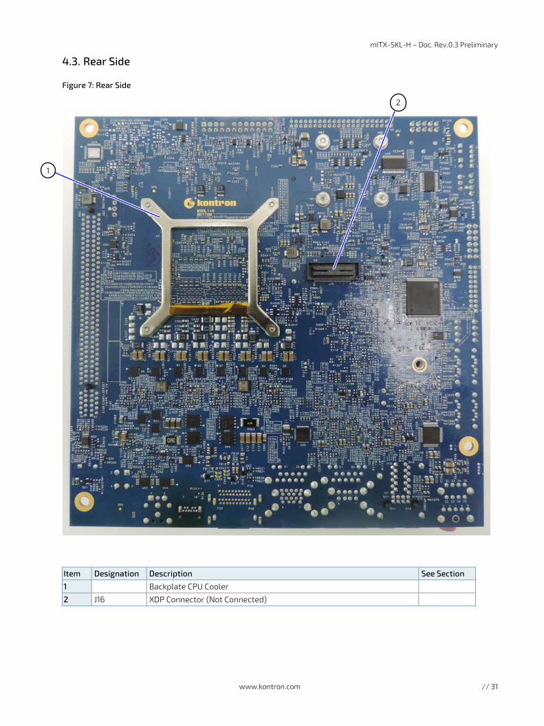
mITX-SKL-H – Doc. Rev.0.3 Preliminary
www.kontron.com // 31
4.3. Rear Side
Figure 7: Rear Side
Item Designation Description See Section
1 Backplate CPU Cooler
2 J16 XDP Connector (Not Connected)
1
2

mITX-SKL-H – Doc. Rev.0.3 Preliminary
www.kontron.com // 32
5/ Connector Definitions The following chapters provide pin definitions and detailed descriptions of all on-board connectors. The connector definitions follow the following notation:
Table 9: Connector definitions
Column Name Description
Pin Shows the pin numbers in the connector.
Signal The mnemonic name of the signal at the current pin. The notation “XX#” states that the signal “XX” is active low.
Type AI: Analogue Input AO: Analogue Output I: Input, TTL compatible if nothing else stated IO: Input / Output. TTL compatible if nothing else stated IOT: Bi-directional tristate IO pin IS: Schmitt-trigger input, TTL compatible IOC: Input / open-collector Output, TTL compatible IOD: Input / Output, CMOS level Schmitt-triggered (Open drain output) NC: Pin not connected O: Output, TTL compatible OC: Output, open-collector or open-drain, TTL compatible OT: Output with tri-state capability, TTL compatible LVDS: Low Voltage Differential Signal PWR: Power supply or ground reference pins
Ioh: Typical current in mA flowing out of an output pin through a grounded load, while the output voltage is > 2.4 V DC (if nothing else stated). Iol: Typical current in mA flowing into an output pin from a VCC connected load, while the output voltage is < 0.4 V DC (if nothing else stated).
Pull U/D On-board pull-up or pull-down resistors on input pins or open-collector output pins
Note Special remarks concerning the signal
Designation Type and number of item described
See section Number of section in this user guide containing a detailed description
The abbreviation TBD is used for specifications that are not available yet or which are not sufficiently specified by the component vendors.

mITX-SKL-H – Doc. Rev.0.3 Preliminary
www.kontron.com // 33
6/ IO-Area Connectors The following connectors are available on the connector panel of the mITX-SKL-H. For information regarding the position of the connectors on the panel, see Chapter 4.2 Connector Panel Side.
6.1. DP Connectors DP1, DP2 (J14)
The mITX-SKL-H Display Port (DP) connectors are based on standard DP type Foxconn 3VD11203-DPA1-4H or similar.
Figure 8: DP Connectors DP1 and DP2
TOP
BOTTOM
Table 10: Pin Assignment DP Connector DP1, DP2 (J14)
Pin Signal Description Type Note 1/21 Lane 0 (+) LVDS 2/22 GND PWR 3/23 Lane 0 (-) LVDS 4/24 Lane 1 (+) LVDS 5/25 GND PWR 6/26 Lane 1 (-) LVDS 7/26 Lane 2 (+) LVDS 8/28 GND PWR 9/29 Lane 2 (-) LVDS 10/30 Lane 3 (+) LVDS 11/31 GND PWR
12/32 Lane 3 (-) LVDS
13/33 Config 1 Aux or DDC selection I
Internally pull down (1 MΩ). Aux channel pin 15/17 or 35/37 selected as default if NC DDC channel pin 15/17 or 35/37, if HDMI adapter used (3.3 V).
14/34 Config 2 (Not used) O Internally connected to GND
15/35 Aux+ Aux Channel (+) or DDC Clk AUX (+) channel used by DP DDC Clk used by HDMI
16/36 GND PWR
17/37 Aux- Aux Channel (-) or DDC Data AUX (-) channel used by DP DDC Data used by HDMI
19 13 9 7 5 3 1
16 10 8 6 4 2
39 37 35 33 31 29 27 25 23 21
40 38 36 34 32 30 28 26 24 22
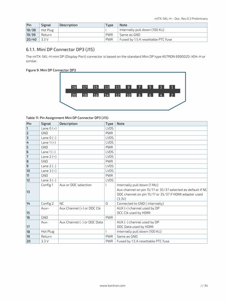
mITX-SKL-H – Doc. Rev.0.3 Preliminary
www.kontron.com // 34
Pin Signal Description Type Note 18/38 Hot Plug I Internally pull down (100 KΩ) 19/39 Return PWR Same as GND 20/40 3.3 V PWR Fused by 1.5 A resettable PTC fuse
6.1.1. Mini DP Connector DP3 (J15) The mITX-SKL-H mini DP (Display Port) connector is based on the standard Mini DP type ASTRON 6990020-X04-H or similar.
Figure 9: Mini DP Connector DP3
Table 11: Pin Assignment Mini DP Connector DP3 (J15)
Pin Signal Description Type Note 1 Lane 0 (+) LVDS 2 GND PWR 3 Lane 0 (-) LVDS 4 Lane 1 (+) LVDS 5 GND PWR 6 Lane 1 (-) LVDS 7 Lane 2 (+) LVDS 8 GND PWR 9 Lane 2 (-) LVDS 10 Lane 3 (+) LVDS 11 GND PWR 12 Lane 3 (-) LVDS
13
Config 1 Aux or DDC selection I Internally pull down (1 MΩ) Aux channel on pin 15/17 or 35/37 selected as default if NC DDC channel on pin 15/17 or 35/37 if HDMI adapter used (3.3V)
14 Config 2 NC O Connected to GND ( internally)
15 Aux+ Aux Channel (+) or DDC Clk AUX (+) channel used by DP
DCC Clk used by HDMI 16 GND PWR
17 Aux- Aux Channel (-) or DDC Data AUX (-) channel used by DP
DDC Data used by HDMI 18 Hot Plug I Internally pull down (100 KΩ) 19 Return PWR Same as GND 20 3.3 V PWR Fused by 1.5 A resettable PTC fuse
1
2
3
4
5
6
7
8
9
10
11
12
13
14
15
16
17
18 18
19
20

mITX-SKL-H – Doc. Rev.0.3 Preliminary
www.kontron.com // 35
6.2. Ethernet Connectors (J5, J8 and J21)
The mITX-SKL-H supports up to four channels of 10/100/1000 Mbit Ethernet:
ETH1 (J21) is based on Intel® Jacksonville i219LM Gigabit PHY with AMT 9.0 support ETH2 (J5), ETH3 (J8) and ETH4 (J8) are based on Intel® Pearsonville i211AT PCI Express controller
In order to achieve the specified performance of the Ethernet port, Category 5 twisted pair cables must be used with 10/100 MB and Category 5E, 6 or 6E with 1 Gbit LAN networks.
Ethernet connectors can be mounted as follows:
Ethernet ETH1/ LAN1 (connector J21) is mounted together with USB Ports 1 and 2 Ethernet ETH2/LAN2 (connector J5) is mounted together with USB Ports 4 and 3 Ethernet ETH3 and Ethernet ETH4 (connector J8) are mounted together
All connectors support activity and Link LEDs
Figure 10: Ethernet Connector with LED Flashing Communication
Table 12: Pin Assignment (RJ45) LAN Connectors (J5, J8, J21)
Pin Signal Type Ioh / Iol Note 1 MDI0+ 2 MDI0- 3 MDI1+ 4 MDI2+ 5 MDI2- 6 MDI1- 7 MDI3+ 8 MDI3-
MDI = Media Dependent Interface.
Signal Description
Signal Description MDI0+ / MDI0- In MDI mode, this is the first pair in 1000Base-T, i.e. the BI_DA+/- pair, and is the transmit pair in
10Base-T and 100Base-TX. In MDI crossover mode, this pair acts as the BI_DB+/- pair, and is the receive pair in 10Base-T and 100Base-TX.
MDI1+ / MDI1- In MDI mode, this is the second pair in 1000Base-T, i.e. the BI_DB+/- pair, and is the receive pair in 10Base-T and 100Base-TX. In MDI crossover mode, this pair acts as the BI_DA+/- pair, and is the transmit pair in 10Base-T and 100Base-TX.
MDI2+ / MDI2- In MDI mode, this is the third pair in 1000Base-T, i.e. the BI_DC+/- pair. In MDI crossover mode, this pair acts as the BI_DD+/- pair.
MDI3+ / MDI3- In MDI mode, this is the fourth pair in 1000Base-T, i.e. the BI_DD+/- pair. In MDI crossover mode, this pair acts as the BI_DC+/- pair.
8 7 6 5 4 3 2 1
LED status:
Orange - 1000 Mb link established
Green - 100 Mb link established
Off - 10 Mb Link established
LED Status
Off – Link is down
Flashing Green-Link is up and active
Steady Green – Link is up ,no activity

mITX-SKL-H – Doc. Rev.0.3 Preliminary
www.kontron.com // 36
6.3. USB Connectors (IO Area)
The mITX-SKL-H board contains an xHCI (Enhanced Host Controller Interface) controller that supports six USB 2.0 ports allowing data transfers up to 480 Mb/s.
The XHCI controller supports up to four USB 3.0 ports allowing data transfers up to 5 Gb/s. Two of the USB 3.0 ports are shared with two of the USB 2.0 ports (USB1 – USB2).
Not all USB 2.0 and USB 3.0 ports are physically connected to the board.
USB 3.0 ports are backward compatible with USB 2.0.
The following USB connectors are available in the IO area:
USB 2.0/3.0 Ports 1, 2, are supplied on the combined 2 x USB connectors (J21) USB 2.0 Ports 3, 4 are supplied on the combined 2xUSB and LAN connector (J5)
Figure 11: USB 2.0 / 3.0 socket
USB 2.0 USB3.0
6.3.1. USB Port 1 and USB Port 2 (J21) USB ports 1 and 2 supports USB 3.0/USB 2.0 and are located on the stacked USB/LAN rear IO connector J21.
Table 13: Pin Assignment USB Port 1 and USB Port 2 (J21)
Pin Signal Type Note Top 18 Tx3+ IO USB 3.0 Tx. Differential Pair (+) 17 TX3- IO USB 3.0 Tx. Differential Pair (-) 16 GND PWR 15 RX3+ IO USB 3.0 Rx. Differential Pair (+) 14 RX3- IO USB 3.0 Rx. Differential Pair (-) 13 GND- PWR 12 D3+ IO USB 2.0 Differential Pair (+) 11 D3- IO USB 2.0 Differential Pair (-) 10 VBus PWR +5 V Supply for USB device Bottom 9 Tx2+ IO USB 3.0 Tx. Differential Pair (+) 8 TX2- IO USB 3.0 Tx. Differential Pair (-) 7 GND PWR 6 RX2+ IO USB 3.0 Rx. Differential Pair (+) 5 RX2- IO USB 3.0 Rx. Differential Pair (-) 4 GND- PWR 3 D2+ IO USB 2.0 Differential Pair (+) 2 D2- IO USB 2.0 Differential Pair (-) 1 VBus PWR +5 V Supply for USB device
Signal Description
Signal Description TXn+, TXn-, RXn+, TXn-, Dn+, Dn-
Differential pair works as serial differential receive/transmit data lines. (n= 2,3)
VBus 5 V supply for external devices. VBUS is supplied during power-down to allow wakeup on USB device activity. Protected by a 1A current limiting IC covering each of the USB port.
mITX-SKL-H – Doc. Rev.0.3 Preliminary
www.kontron.com // 37
6.3.2. USB Port 3 and USB Port 4 (J5) USB port 3 and 4 supports USB2.0 and are located on the stacked USB/LAN rear IO connector J5.
Table 14: Pin Assignment USB Port 3 and USB Port 4 (J5)
Pin Signal Type Note Top 8 GND- PWR 7 D6+ IO USB 2.0 differential pair (+) 6 D6- IO USB 2.0 differential pair (-) 5 VBus PWR Bottom 4 GND- PWR 3 D7+ IO USB 2.0 differential pair (+) 2 D7- IO USB 2.0 differential pair (-) 1 VBus PWR
Signal Description
Signal Description Dn+, Dn- Differential pair works as serial differential receive/transmit data lines.
(n= 6,7) VBus 5 V supply for external devices.
VBUS is supplied during power-down to allow wakeup on USB device activity. Protected by a 1A current limiting IC covering each of the USB port.

mITX-SKL-H – Doc. Rev.0.3 Preliminary
www.kontron.com // 38
For USB2.0 cabling it is required to use only HiSpeed USB cable, specified in USB2.0 standard:
Figure 12: USB 2.0 High Speed Cable
For USB3.0 cabling it is required to use only HiSpeed USB cable, specified in USB3.0 standard:
Figure 13: USB 3.0 High Speed Cable
W
G
BR
Polyvinyl Chloride (PVC) Jacket
Outer Shield ≥ 65% Interwoven Tinned Copper Braid
Inner Shield Aluminum Metallized Polyester
28 AWG Tinned Copper Drain Wire
Twisted Signaling Pair: White: D- Green: D+
On-Twisted Power Pair: Red: VBUS Black: Power Ground
UTP Signal Pair
SDP Signal Pair
Jacket
Ground
Filler, optional
Braid
Power
SDP Signal Pair
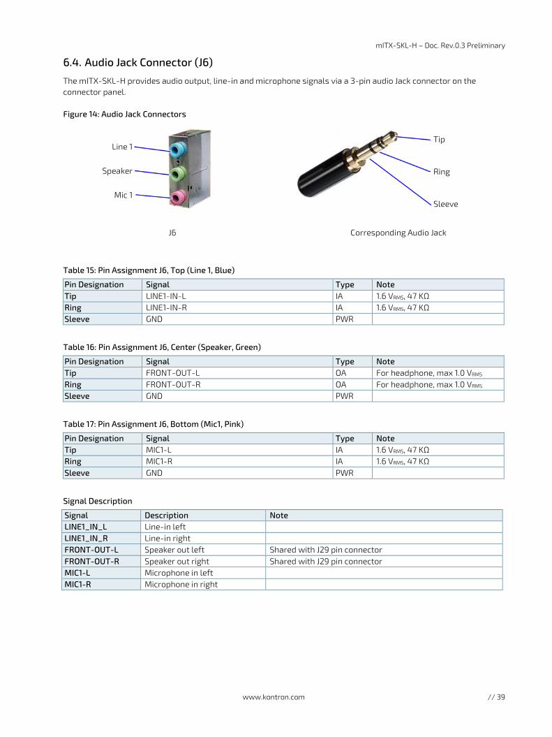
mITX-SKL-H – Doc. Rev.0.3 Preliminary
www.kontron.com // 39
6.4. Audio Jack Connector (J6)
The mITX-SKL-H provides audio output, line-in and microphone signals via a 3-pin audio Jack connector on the connector panel.
Figure 14: Audio Jack Connectors
J6 Corresponding Audio Jack
Table 15: Pin Assignment J6, Top (Line 1, Blue)
Pin Designation Signal Type Note Tip LINE1-IN-L IA 1.6 VRMS, 47 KΩ Ring LINE1-IN-R IA 1.6 VRMS, 47 KΩ Sleeve GND PWR
Table 16: Pin Assignment J6, Center (Speaker, Green)
Pin Designation Signal Type Note Tip FRONT-OUT-L OA For headphone, max 1.0 VRMS Ring FRONT-OUT-R OA For headphone, max 1.0 VRMS Sleeve GND PWR
Table 17: Pin Assignment J6, Bottom (Mic1, Pink)
Pin Designation Signal Type Note Tip MIC1-L IA 1.6 VRMS, 47 KΩ Ring MIC1-R IA 1.6 VRMS, 47 KΩ Sleeve GND PWR
Signal Description
Signal Description Note LINE1_IN_L Line-in left LINE1_IN_R Line-in right FRONT-OUT-L Speaker out left Shared with J29 pin connector FRONT-OUT-R Speaker out right Shared with J29 pin connector MIC1-L Microphone in left MIC1-R Microphone in right
Tip
Ring
Sleeve
Line 1
Speaker
Mic 1

mITX-SKL-H – Doc. Rev.0.3 Preliminary
www.kontron.com // 40
6.5. Power Connector DC Jack (J32)
The mITX-SKL-H board is designed to be supplied from either a DC jack or a standard 4-pin ATX+12 V power supply, see chapter 7.1. Power Connector 4-pin ATX+12 V (J31)
For more information see Chapter 3.7 Power Consumption regarding input tolerances on +12 V and +24 V or refer to the ATX Specification version 2.2.
Hot plugging of the power connectors is not allowed. Hot plugging might damage the board.
When connecting to the motherboard, turn off main supply to make sure all the power lines are turned off.
Table 18: Pin Assignment DC Jack (J32)
Pin Signal Type Note 1 +12 V to +24 V PWR 2 SIG O Unused 3 +12 V to +24 V PWR 4 GND PWR 5 GND PWR S1 Shield PWR SHIELD and GND are electrically connected S2 Shield PWR SHIELD and GND are electrically connected S3 Shield PWR SHIELD and GND are electrically connected
Signal Description
Signal Description Shield SHIELD and GND are electrically connected GND Power Supply ground signal

mITX-SKL-H – Doc. Rev.0.3 Preliminary
www.kontron.com // 41
7/ Internal Connectors
7.1. Power Connector 4-pin ATX+12 V (J31)
The mITX-SKL-H boards are designed to be supplied from a standard 4-pin ATX+12 V supply or an AC adapter.
For more information see Chapter 3.7 Power Consumption regarding input tolerances on +12 V and +24 V or refer to the ATX Specification version 2.2.
Hot plugging of the power connectors is not allowed. Hot plugging might damage the board.
When connecting to the motherboard, turn off main supply to make sure all the power lines are turned off.
Figure 15: 4-Pin ATX +12 V Power Connector
Table 19: Pin Assignment 4-Pin ATX 12 V Power Connector (J31)
Pin Signal Type Note 1 GND PWR 2 GND PWR 3 +12 V to +24 V PWR +24 V can be supplied to 4-pin ATX 12 V connector 4 +12 V to +24 V PWR +24 V can be supplied to 4-pin ATX 12 V connector
Signal Description
Signal Description GND Power Supply ground signal
1 2
3 4

mITX-SKL-H – Doc. Rev.0.3 Preliminary
www.kontron.com // 42
7.2. Fan Connectors (J33, J34)
The SYSTEM FAN (J34) can be used to power, control and monitor a fan for chassis ventilation etc. The CPU FAN (J33) is used for the connection of the FAN for the CPU. The 4-pin connector is recommended for driving a 4-wire type Fan, in order to implement FAN speed control. 3-wire Fan support is also possible, but no Fan speed control is integrated.
Figure 16: Fan Connector
Table 20: Pin Assignment 4-Pin Fan Support Mode
Pin Signal Description Type 1 GND Ground PWR 2 12 V Power +12 V PWR 3 TACHO Tacho signal I 4 PWM PWM Output O-3.3
Table 21: Pin Assignment 3-Pin Fan Support Mode
Pin Signal Description Type 1 GND Ground PWR 2 12 V Power +12 V PWR 3 TACHO Tacho signal I 4 NC Not used
Signal Description
Signal Description Type GND Power Supply GND signal PWR 12 V +12 V supply for fan. A maximum of 600 mA can be supplied from this pin. PWR TACHO Tacho input signal from the fan, for rotation speed supervision RPM (Rotations Per Minute).
The signal shall be generated by an open collector transistor or similar. A 4.7 Ω pull-up resistor to +12 V is on-board. The signal has to be pulsed and the on-board circuit is prepared for two pulses per rotation.
I
PWM PWM output signal for FAN speed control O

mITX-SKL-H – Doc. Rev.0.3 Preliminary
www.kontron.com // 43
7.3. SATA (Serial ATA) Disk Interfaces (J10, J11, J12, J13)
The mITX-SKL-H supports an integrated SATA host controller (PCH in the CM236 chipset) that supports independent DMA operation on six ports. One device can be installed on each port for a maximum of six SATA devices via four SATA connectors, one mSATA connector and one M.2 SATA connector. A point-to-point interface (SATA cable) is used for host to device connections. Data transfer rates of up to 6.0 Gb/s,3.0 GB/s, and1.5 Gb/s are supported on all SATA ports.
Before installing OS on a SATA drive make sure the drive is not a former member of a RAID system. If this is the case, some hidden data on the disk must be erased. To do this, connect two SATA drives and select RAID in BIOS. Save settings and select <Ctrl> <I> while booting to enter the RAID setup menu. Now the hidden RAID data will be erased from the selected SATA drive.-TBD
Supported SATA features:
AHCI (Advanced Host Controller Interface) 1.3 and 1.3.1 2 to 4-drive RAID 0 (data striping) 2-drive RAID 1 (data mirroring) 3 to 4-drive RAID 5 (block-level striping with parity) 4-drive RAID 10 (data striping and mirroring) 2 to 4-drive matrix RAID, different parts of a single drive can be assigned to different RAID devices NCQ (Native Command Queuing). NCQ is for faster data access Swap bay support ( not supported on mSATA) -TBD Intel® Rapid Recover Technology Intel® Smart Response Technology
Figure 17: SATA Connector
Table 22: Pin Assignment SATA1 (J10), SATA2 (J12), SATA3 (J11) and SATA4 (J13) Connectors:
Pin Signal Type Ioh / Iol Note 1 GND PWR 2 SATA# TX+ 3 SATA# TX- 4 GND PWR 5 SATA# RX- 6 SATA# RX+ 7 GND PWR
Signal Description
Signal Description SATA# RX+ / RX- Host receiver differential signal pair SATA# TX+ / TX- Host transmitter differential signal pair GND Power Supply GND signal “#” specifies 2,3,6 or 7 depending on SATA port.
Available Cable Kit
PN 821035 Cable SATA 500 mm
1234567

mITX-SKL-H – Doc. Rev.0.3 Preliminary
www.kontron.com // 44
7.4. USB 3.0 Internal Connectors (J3, J27)
The following mITX-SKL-H USB ports are available on internal connectors:
USB 3.0 Port 5 and 6 on the internal USB 3.0 connector (J3) USB 2.0 Port 7 and 8 on the internal FRONT PANEL connector (J27)
Table 23: Pin Assignment USB 3.0 Internal Connector (J3)
Pin Signal Type Ioh / Iol Note 1 V_VBUS PWR 2 RX5- USB 3.0 3 RX5+ USB 3.0 4 GND PWR 5 TX5- USB 3.0 6 TX5+ USB 3.0 7 GND PWR 8 D5- USB 2.0 9 D5+ USB 2.0 10 NC 11 D4+ USB 2.0 12 D4- USB 2.0 13 GND PWR 14 TX4+ USB 3.0 15 TX4- USB 3.0 16 GND PWR 17 RX4+ USB 3.0 18 RX4- USB 3.0 19 V_VBUS PWR 20 KEY( NC)
Signal Description
Signal Description V_VBUS +5V Supply for USB Device RX#+/- USB 3.0 receiver differential signal pair TX#+/- USB 3.0 transmitter differential signal pair D#+/- USB 2.0 differential signal pair GND Power Supply GND signal

mITX-SKL-H – Doc. Rev.0.3 Preliminary
www.kontron.com // 45
7.5. Headphone/Speaker Connector (J29)
The mITX-SKL-H headphone interface is available through the 4-pin connector J29. This output is shared with the Speaker Audio Jack connector (J6, green).
Figure 18: Speaker Connector
Table 24: Pin Assignment Speaker Connector (J29)
Pin Signal Type Note 1 GND PWR 2 HPOUT-L AO 3 GND PWR 4 HPOUT-R AO
Signal Description
Signal Description HPOUT-L Headphone output left HPOUT-R Headphone output right GND Power Supply GND signal
7.6. SPDIF-OUT Connector (J30)
The mITX-SKL-H digital audio interface (electrical SPDIF-Out) is available through the 2-pin connector J33 and can be used to implement eight (7.1) High Definition Audio channels. The audio interface is based on a high fidelity 8-channel HD audio codec that is compatible with the Intel HD Audio specification and provides:
Stereo 24-bit resolution Up to 192 kHz sample rate for DACs/ADCs Maximum Signal-to-Noise Ratio (SNR) of 90 dB 16/20/24-bit S/PDIF TX outputs supporting 48 K/96 K/44.1 K/88.2 KHz sample rates.
Figure 19: SPDIF-OUT Connector
Table 25: Pin Assignment SPDIF-OUT Connector (J30)
Pin Signal Type Note 1 SPDIF_OUT O-3.3 2 GND PWR
Signal Description
Signal Description SPDIF_OUT Sony/Philips Digital Interface (SPDIF) audio output signal GND Power Supply GND signal
1 2 3 4
1 2
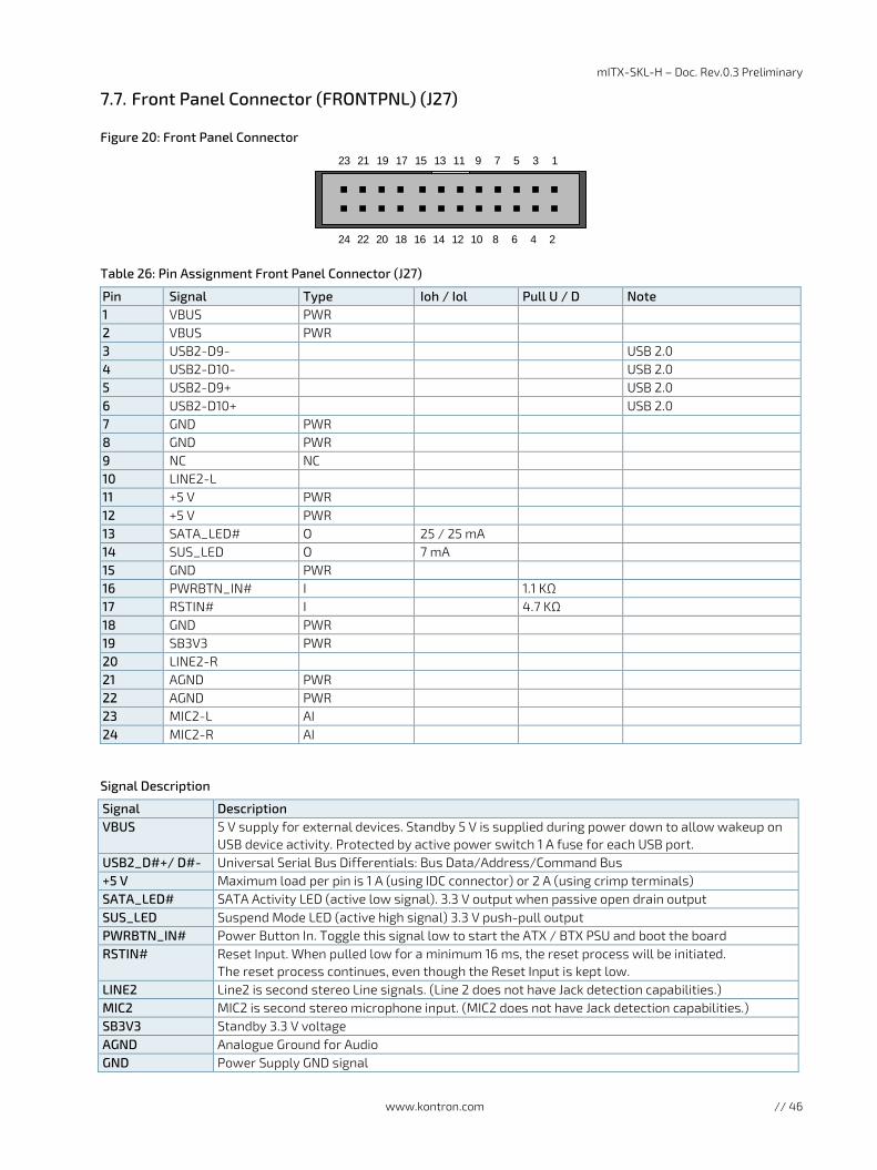
mITX-SKL-H – Doc. Rev.0.3 Preliminary
www.kontron.com // 46
7.7. Front Panel Connector (FRONTPNL) (J27)
Figure 20: Front Panel Connector
Table 26: Pin Assignment Front Panel Connector (J27)
Pin Signal Type Ioh / Iol Pull U / D Note 1 VBUS PWR 2 VBUS PWR 3 USB2-D9- USB 2.0 4 USB2-D10- USB 2.0 5 USB2-D9+ USB 2.0 6 USB2-D10+ USB 2.0 7 GND PWR 8 GND PWR 9 NC NC 10 LINE2-L 11 +5 V PWR 12 +5 V PWR 13 SATA_LED# O 25 / 25 mA 14 SUS_LED O 7 mA 15 GND PWR 16 PWRBTN_IN# I 1.1 KΩ 17 RSTIN# I 4.7 KΩ 18 GND PWR 19 SB3V3 PWR 20 LINE2-R 21 AGND PWR 22 AGND PWR 23 MIC2-L AI 24 MIC2-R AI
Signal Description
Signal Description VBUS 5 V supply for external devices. Standby 5 V is supplied during power down to allow wakeup on
USB device activity. Protected by active power switch 1 A fuse for each USB port. USB2_D#+/ D#- Universal Serial Bus Differentials: Bus Data/Address/Command Bus +5 V Maximum load per pin is 1 A (using IDC connector) or 2 A (using crimp terminals) SATA_LED# SATA Activity LED (active low signal). 3.3 V output when passive open drain output SUS_LED Suspend Mode LED (active high signal) 3.3 V push-pull output PWRBTN_IN# Power Button In. Toggle this signal low to start the ATX / BTX PSU and boot the board RSTIN# Reset Input. When pulled low for a minimum 16 ms, the reset process will be initiated.
The reset process continues, even though the Reset Input is kept low. LINE2 Line2 is second stereo Line signals. (Line 2 does not have Jack detection capabilities.) MIC2 MIC2 is second stereo microphone input. (MIC2 does not have Jack detection capabilities.) SB3V3 Standby 3.3 V voltage AGND Analogue Ground for Audio GND Power Supply GND signal
1357911131517192123
24681012141618202224

mITX-SKL-H – Doc. Rev.0.3 Preliminary
www.kontron.com // 47
Available Cable Kit
PN 821042 Cable Front Panel Open-End, 300 mm
7.8. Serial COM1 Port (J22)
The mITX-SKL-H supports one RS232 serial port.
Figure 21: Serial COM 1
Table 27: Pin Assignment Serial COM1 Port (J22)
Pin Signal Type Ioh / Iol Pull U / D Note 1 DCD I 2 DSR I 3 RxD I 4 RTS O 5 TxD O 6 CTS I 7 DTR O 8 RI I 9 GND PWR 10 5V PWR The COM1 5 V supply is fused with common
1.5 A resettable fuse.
Signal Description
Signal Description TxD Transmitted Data, sends data to the communications link. The signal is set to the marking state
(-12 V) on hardware reset when the transmitter is empty or when loop mode operation is initiated. RxD Received Data, receives data from the communications link. DTR Data Terminal Ready, indicates to the modem etc. that the on-board UART is ready to establish
communication link. DSR Data Set Ready, indicates that the modem etc. is ready to establish a communications link. RTS Request To Send, indicates to the modem etc. that the on-board UART is ready to exchange data. CTS Clear To Send, indicates that the modem or data set is ready to exchange data. DCD Data Carrier Detect, indicates that the modem or data set has detected the data carrier. RI Ring Indicator, indicates that the modem has received a ringing signal from the telephone line. GND Power Supply GND signal
13579
246810
mITX-SKL-H – Doc. Rev.0.3 Preliminary
www.kontron.com // 48
DB9 adapter cables are available to implement standard COM ports on chassis.
Available Cable Kit (DB9 adapter cables)
PN 821017 - 100 mm or PN 821016 - 200 mm
7.9. Serial COM2 Port (J35)
The mITX-SKL-H supports one RS422/485 serial port. Full-duplex and half-duplex can be configured from the BIOS menu.
Table 28: Pin Assignment Serial COM 2 Port (J35)
Pin Signal Type Ioh / Iol Pull U / D Note 1 RS485_TX1- O Data (-) in half-duplex mode 2 RS485_RX1+ I 3 RS485_TX1+ O Data (+) in half-duplex mode 4 RS485_RX1- I 5 GND PWR
Signal Description
Signal Description RS485_TX1+/- Transmitted Data differential pair, sends data to the communications link RS485_RX1+/- Received Data differential pair, receives data from the communications link. GND Power Supply GND signal

mITX-SKL-H – Doc. Rev.0.3 Preliminary
www.kontron.com // 49
7.10. LVDS FLAT PANEL CONNECTOR (J7)
The mITX-SKL-H LVDS connector is based on a 40-pin connector type Samtec SHF-120-10-F-D.
Figure 22: LVDS Connector
Table 29: Pin Assignment LVDS Flat Panel Connector (J7)
Pin Signal Type Note 1 +12 V PWR Max. 0.5 A 2 +12 V PWR Max. 0.5 A 3 +12 V PWR Max. 0.5 A 4 +12 V PWR Max. 0.5 A 5 +12 V PWR Max. 0.5 A 6 GND PWR 7 +5 V PWR Max. 0.5 A 8 GND PWR 9 LCDVCC PWR Max. 0.5 A 10 LCDVCC PWR Max. 0.5 A 11 DDC CLK OT 2.2 KΩ, 3.3 V 12 DDC DATA OT 2.2 KΩ, 3.3 V 13 BKLTCTL OT 3.3 V level 14 VDD ENABLE OT 3.3 V level 15 BKLTEN# OT 3.3 V level 16 GND PWR 17 LVDS A0- LVDS 18 LVDS A0+ LVDS 19 LVDS A1- LVDS 20 LVDS A1+ LVDS 21 LVDS A2- LVDS 22 LVDS A2+ LVDS 23 LVDS ACLK- LVDS 24 LVDS ACLK+ LVDS 25 LVDS A3- LVDS 26 LVDS A3+ LVDS 27 GND PWR 28 GND PWR 29 LVDS B0- LVDS 30 LVDS B0+ LVDS 31 LVDS B1- LVDS 32 LVDS B1+ LVDS 33 LVDS B2- LVDS 34 LVDS B2+ LVDS 35 LVDS BCLK- LVDS 36 LVDS BCLK+ LVDS 37 LVDS B3- LVDS 38 LVDS B3+ LVDS 39 GND PWR 40 GND PWR
13579111315171921232527293133353739
246810121416182022242628303234363840

mITX-SKL-H – Doc. Rev.0.3 Preliminary
www.kontron.com // 50
The on-board LVDS connector supports single and dual channel, 18/24 bit SPWG panels, up to a resolution of 1600x1200 px or 1920x1080 px and with limited frame rate up to 1920x1200 px.
Signal Description
Signal Description LVDS A0…A3 LVDS A Channel data LVDS ACLK LVDS A Channel clock LVDS B0…B3 LVDS B Channel data LVDS BCLK LVDS B Channel clock BKLTCTL Backlight control, PWM signal to implement voltage in the range 0 V-3.3 V BKLTEN# Backlight Enable signal (active low) VDD ENABLE Output display enable LCDVCC VCC supply to the display. 5 V or 3.3 V (1 A maximum) selected in BIOS setup menu.
Power sequencing depends on LVDS panel selection. DDC CLK DDC Channel Clock GND Power Supply GND signal
Windows API will be available to operate the BKLTCTL signal. Some Inverters have a limited voltage range 0- 2.5V for this signal: If voltage is > 2.5V the Inverter might latch up. Some inverters generate noise on the BKLTCTL signal, causing the LVDS transmission to fail (corrupted picture on the display). By adding a 1 KΩ resistor in series with this signal, mounted at the inverter end of the cable kit, the noise is limited and the picture is stable.
If the Backlight Enable is required to be active high then check the BIOS Setup menus.

mITX-SKL-H – Doc. Rev.0.3 Preliminary
www.kontron.com // 51
7.11. Feature Connector (J26)
Figure 23: Feature Connector
Table 30: Pin Assignment Feature Connector (J26)
Pin Signal Type Ioh / Iol Pull U / D Note 1 INTRUDER# I 2 MΩ / … Pull-up to on-board Battery 2 SMBC /4 mA 10 KΩ /… Pull-up to +3.3 V dual (+3.3 V or SB
3.3 V) 3 S4# O 25 /25 mA 4 SMBD /4 mA 10 KΩ /… Pull-up to +3.3 V dual (+3.3 V or SB
3.3 V) 5 PWR_OK O 25 /25 mA 6 EXT_BAT PWR 7 NC 8 NC 9 SB3V3 PWR 10 SB5V PWR 11 GPIO0 IOT 12 GPIO1 IOT 13 GPIO2 IOT 14 GPIO3 IOT 15 GPIO4 IOT 16 GPIO5 IOT 17 GPIO6 IOT 18 GPIO7 IOT 19 GND PWR 20 GND PWR 21 GPIO8 I 22 GPIO9 I 23 GPIO10 I 24 GPIO11 I 25 GPIO12 I 26 GPIO13 IOT 27 GPIO14 IOT 28 GPIO15 IOT 29 GPIO16 IOT 30 GPIO17 IOT 31 GND PWR 32 GND PWR 33 EGCLK O 8 /8 mA 34 EGCS# O 8 /8 mA 35 EGAD 8 /8 mA 36 TMA0 O 37 +12 V PWR 38 GND PWR 39 NC 40 NC 41 GND PWR
135791113151719212325272931333537394143
2468101214161820222426283032343638404244

mITX-SKL-H – Doc. Rev.0.3 Preliminary
www.kontron.com // 52
Pin Signal Type Ioh / Iol Pull U / D Note 42 GND PWR 43 GND PWR 44 S3# O 25 /25 mA
Signal Description
Signal Description INTRUDER# Also known as, CASE OPEN. Used to detect if the system case has been opened. This signal’s status
is readable, so it may be used like a GPI when the Intruder switch is not required. SMBC SMBus Clock signal SMBD SMBus Data signal S3# S3 sleep mode, active low output, optionally used to deactivate external system. S4# S4 sleep mode, active low output, optionally used to deactivate external system. PWR_OK Power OK, signal is high if no power failures are detected.
(This is not the same as the P_OK signal generated by ATX PSU). EXT_BAT (EXTernal BATtery) option for connecting + terminal of an external primary cell battery
(2.5 - 3.47 V) (– terminal connected to GND). The external battery is protected against charging and can be used with / without the on-board battery installed.
SB3V3 Maximum load is 0.75 A (1.5 A < 1 sec.) SB5 V StandBy +5 V supply. GPIO0..17 General Purpose Inputs /Output. These signals may be controlled or monitored through the use of
the KT-API-V2 (Application Programming Interface). EGCLK Extend GPIO Clock signal EGAD Extend GPIO Address Data signal EGCS# Extend GPIO Chip Select signal, active low TMA0 Timer Output +12 V Max. load is 0.75 A (1.5 A < 1 sec.) GND Power Supply GND signal
The GPIOs are controlled via the ITE IT8528E Embedded Controller. Each GPIO has 100 pF to ground, clamping diode to 3.3 V and has multiplexed functionality. Some pins can be DAC (Digital to Analogue Converter) output, PWM (Pulse Width Modulated) signal output, ADC (Analogue to Digital Converter) input, TMRI (Timer Counter Input), WUI (Wake Up Input), RI (Ring Indicator Input) or some special function.
Signal Description IT8528E Embedded Controller
Signal IT8528E Pin Name Type Description GPIO0 DAC0/GPJ0 AO/IOS GPIO1 DAC1/GPJ1 AO/IOS GPIO2 DAC2/GPJ2 AO/IOS GPIO3 DAC3/GPJ3 AO/IOS GPIO4 PWM2/GPA2 O8/IOS GPIO5 PWM3/GPA3 O8/IOS GPIO6 PWM4/GPA4 O8/IOS GPIO7 PWM5/GPA5 O8/IOS GPIO8 ADC0/GPI0 AI/IS GPIO9 ADC1/GPI1 AI/IS GPI10 ADC2/GPI2 AI/IS GPI11 ADC3/GPI3 AI/IS GPI12 ADC4/WUI28/GPI4 AI/IS/IS GPI13 RI1#/WUI0/GPD0 IS/IS/IOS GPI14 RI2#/WUI1/GPD1 IS/IS/IOS GPI15 TMRI0/WUI2/GPC4 IS/IS/IOS GPI16 TMRI1/WUI3/GPC6 IS/IS/IOS GPI17 L80HLAT/BAO/WUI24/GPE0 O4/O4/IS/IOS

mITX-SKL-H – Doc. Rev.0.3 Preliminary
www.kontron.com // 53
Available cable kit:
PN 1052-5885 Cable, Feature 44pol 1 to1, 300 mm

mITX-SKL-H – Doc. Rev.0.3 Preliminary
www.kontron.com // 54
7.12. SPI Connector (J9)
The SPI Connector is normally not used. If however a SPI BIOS is connected via the SPI Connector, then the board attempts to boot from it.
Figure 2: SPI Connector 12-Pin Connector
Table 31: Pin Assignment SPI Connector (J9)
Pin Signal Type Ioh / Iol Pull U / D Note 1 CLK 2 SB3V3 PWR 3 CS0# I 4 ADDIN IO - / 10 KΩ 5 V_SPI 10 KΩ /- 6 NC 7 MOSI IO 10 KΩ /- 8 ISOLATE# IO 100 KΩ 9 MISO IO 10 GND PWR 11 SPI_I02_#WP IO 1 KΩ/- 12 SPI_I03_#HOLD IO 1 KΩ
Signal Description
Signal Description CLK Serial Clock V_SPI 3.3 V Standby Voltage power line. Normal output power, but when the motherboard is turned off,
the on-board SPI Flash can be a 3.3 V power sourced via this pin. SB3V3 3.3 V Standby Voltage power line. Normal output power, but when the motherboard is turned off,
the on-board SPI Flash can be 3.3 V power sourced via this pin. CS0# CS0# Chip Select 0, active low ADDIN ADDIN input signal must be NC MOSI Master Output, Slave Input ISOLATE# The ISOLATE# input, active low, is normally NC, but must be connected to GND when
programming the SPI flash. Power Supply to the Motherboard must be turned off when loading SPI flash. The pull up resistor is connected via diode to 5 V Standby.
MISO Master Input, Slave Output SPI_IO2_#WP SPI Data I/O: A bidirectional signal used to support Dual IO Fast Read, Quad IO Fast Read and
Quad Output Fast Read modes. The signal is not used in Dual Output Fast Read mode. SPI_IO3_#HOLD SPI Data I/O: A bidirectional signal used to support Dual IO Fast Read, Quad IO Fast Read and
Quad Output Fast Read modes. The signal is not used in Dual Output Fast Read mode. GND Power Supply ground signal
1 3 5 7 9
2 4 6 8 10 12
11

mITX-SKL-H – Doc. Rev.0.3 Preliminary
www.kontron.com // 55
7.13. SPI Connector for External Fast GPIO Expander (J36)
The mITX-SKL-H supports a 6-pin external SPI for external fast General Purpose Input/Output (GPIO) support. The configurable input output pins are implemented to support the mITX –SKL-H with clock, chip select and two configurable signal options (Master Slave or Slave to Master).
Table 32: Pin Assignment SPI connector for Fast GPIO Expander (J36)
Pin Signal Type Ioh / Iol Pull U / D Note 1 SB3V3 PWR 2 SPI MOSI I/O 3 SPI MISO I/O 4 SPI CLK O 5 SPI CS# O 6 GND PWR
Signal Description
Signal Description SB3V3 3.3 V Standby Voltage power line. Normal output power, but when the motherboard is turned off,
the on-board SPI Flash connector can supply a 3.3 V power source via this pin SPI MOSI SPI signal (Master Out Slave In) SPI MISO SPI signal (Master In Slave Out) SPI CLK SPI signal (Clock) SPI CS# SPI signal (Chip Select) GND Power Supply ground signal

mITX-SKL-H – Doc. Rev.0.3 Preliminary
www.kontron.com // 56
7.14. Switches and Jumpers
7.14.1. “Always On” Jumper Setting (J39) When jumper J39 is installed in the Pin 1-2 “Always On” position, the board will automatically power up, when the external power supply is switched ON.
When the jumper is not mounted, then the “Always On” feature is disabled and it might be necessary to activate the power on button (PWRBTN_IN#) at the Front Panel connector (FRONTPNL) in order to switch on the board.
Figure 24: Jumper “Always On”
Table 33: Jumper Description (J39)
J39 position Description
Pin 1-2 Pin 2-3 X - Always On( Auto powers on when the power is switched on) - X Default position ( Always On feature is disabled) - - Same as default X = Jumper set
Don´t leave the jumper in position 1-2. If power is disconnected, the battery will fully deplete
within a few weeks.
Pin 3 (Bottom)
Pin 1 (Top)
Pin 2 (Middle)

mITX-SKL-H – Doc. Rev.0.3 Preliminary
www.kontron.com // 57
7.14.2. “Clear CMOS” Jumper ( J37) The “Clear CMOS” jumper (J37) can be used to reset the RTC clock and drain the RTC Well.
The jumper has one position: Pin 1-2 and not mounted (default position). More information on setting the “Clear CMOS” jumper can be found in the table below.
Table 34: “Clear CMOS” Jumper Description (J37)
J37 position Description
Pin 1-2 X Clear CMOS RTC content
(Board does not boot with the jumper in this position) - Default position X = Jumper is set
Do not leave the jumper in position 1-2, otherwise if the power is disconnected, the battery will fully deplete within a few weeks.
7.14.3. Load BIOS Default Jumper (J38) The “Load BIOS Default” jumper (J38) can be used to recover from incorrect BIOS settings. For example, an incorrect BIOS setting that causes the attached display not to turn on can be erased by this jumper.
Table 35: Load BIOS Default Jumper Description (J38)
J38 position Description
Pin 1-2 X Loads default BIOS settings and erases the password
(Board does not boot with the jumper in this position) - Default position X = Jumper is set
Do not leave the jumper in position 1-2, otherwise if the power is disconnected, the battery will fully deplete within a few weeks.
To load default BIOS settings and erase password:
1. Turn off power completely (no +12 V to +24 V supply). 2. Place the jumper to position 1-2. 3. Turn on power. 4. Motherboard beeps fast 20 times and turns off. 5. Turn off power. 6. Disconnect the jumper. 7. Turn on power, use the Power On Button (PWRBTN_IN#) if required to boot.
Motherboard might automatically reboot a few times. Wait until booting is completed.

mITX-SKL-H – Doc. Rev.0.3 Preliminary
www.kontron.com // 58
7.15. Slot Connectors (PCIe, miniPCIe, SIM-Card and M.2)
The mITX-SKL-H supports the following slot connectors:
1 xPCIe x16 (16-lane) PCI Express port (J4) 1 x miniPCIe or mSATA, USB 2.0 (J17) 1x SIM-card socket (J20) 1x optional M.2 (J18)
7.15.1. PCI-Express x16 Connector (J4) The mITX-SKL-H supports PCI express x 16 via slot J4 and supports PEG Bifurcation. The PCIexpress lanes can be divided into:
2x PCIex8 1x PCIe x8 + 2x PCIe x4
A Riser Card with bifurcation is required for PEG Bifurcation to function.
The 16-lane (x16) PCI Express (J4) (PCIe 2.0 and PCIe 3.0) port can be used for external PCI express cards inclusive graphics card. The maximum theoretical bandwidth using 16 lanes is 16 GB/s.
Table 36: Pin Assignment PCIe (x16) Slot Connector (J4)
Pin
Side B Connector Side A Connector Name Description Name Description
1 +12V +12 V power NC NC 2 +12V +12 V power +12V +12 V power 3 +12V +12 V power +12V +12 V power 4 GND Ground GND Ground 5 SMCLK SMBus clock NC NC 6 SMBDAT SMBus data NC NC 7 GND Ground NC NC 8 +3V3 +3.3 V power NC NC 9 NC NC +3V3 +3.3 V power 10 SB3V3 3.3v V power +3V3 +3.3 V power 11 WAKE# Link Reactivation RST# Reset Mechanical Key 12 NC NC GND Ground 13 GND Ground PCIEx16CLK Reference Clock
Differential pair 14 PEG_TXP[0] Transmitter Lane 0, Differential pair
PCIE_x16 CLK# 15 PEG_TXN[0] GND Ground 16 GND Ground PEG_RXP[0] Receiver Lane 0,
Differential pair 17 CLKREQ Clock request PEG_RXN[0] 18 GND Ground GND Ground 19 PEG_TXP[1] Transmitter Lane 1,
Differential pair NC NC
20 PEG_TXN[1] GND Ground 21 GND Ground PEG_RXP[1] Receiver Lane 1,
Differential pair 22 GND Ground PEG_RXN[1] 23 PEG_TXP[2] Transmitter Lane 2,
Differential pair GND Ground
24 PEG_TXN[2] GND Ground 25 GND Ground PEG_RXP[2] Receiver Lane 2,
Differential pair 26 GND Ground PEG_RXN[2] 27 PEG_TXP[3] Transmitter Lane 3,
Differential pair GND Ground
28 PEG_TXN[3] GND Ground 29 GND Ground PEG_RXP[3] Receiver Lane 3,
Differential pair 30 NC NC PEG_RXN[3] 31 CLKREQ Clock request GND Ground 32 GND Ground NC NC

mITX-SKL-H – Doc. Rev.0.3 Preliminary
www.kontron.com // 59
Pin
Side B Connector Side A Connector Name Description Name Description
33 PEG_TXP[4] Transmitter Lane 4, Differential pair
NC NC 34 PEG_TXN[4] GND Ground 35 GND Ground PEG_RXP[4] Receiver Lane 4,
Differential pair 36 GND Ground PEG_RXN[4] 37 PEG_TXP[5] Transmitter Lane 5,
Differential pair GND Ground
38 PEG_TXN[5] GND Ground 39 GND Ground PEG_RXP[5] Receiver Lane 5,
Differential pair 40 GND Ground PEG_RXN[5] 41 PEG_TXP[6] Transmitter Lane 6,
Differential pair GND Ground
42 PEG_TXN[6] GND Ground 43 GND Ground PEG_RXP[6] Receiver Lane 6,
Differential pair 44 GND Ground PEG_RXN[6] 45 PEG_TXP[7] Transmitter Lane 7,
Differential pair GND Ground
46 PEG_TXN[7] GND Ground 47 GND Ground PEG_RXP[7] Receiver Lane 7,
Differential pair 48 CLKREQ Clock request PEG_RXN[7] 49 GND Ground GND Ground 50 PEG_TXP[8] Transmitter Lane 8,
Differential pair NC NC
51 PEG_TXN[8] GND Ground 52 GND Ground PEG_RXP[8] Receiver Lane 8,
Differential pair 53 GND Ground PEG_RXN[8] 54 PEG_TXP[9] Transmitter Lane 9,
Differential pair GND Ground
55 PEG_TXN[9] GND Ground 56 GND Ground PEG_RXP[9] Receiver Lane 9,
Differential pair 57 GND Ground PEG_RXN[9] 58 PEG_TXP[10] Transmitter Lane 10,
Differential pair GND Ground
59 PEG_TXN[10] GND Ground 60 GND Ground PEG_RXP[10] Receiver Lane 10,
Differential pair 61 GND Ground PEG_RXN[10] 62 PEG_TXP[11] Transmitter Lane 11,
Differential pair GND Ground
63 PEG_TXN[11] GND Ground 64 GND Ground PEG_RXP[11] Receiver Lane 11,
Differential pair 65 GND Ground PEG_RXN[11] 66 PEG_TXP[12] Transmitter Lane 12,
Differential pair GND Ground
67 PEG_TXN[12] GND Ground 68 GND Ground PEG_RXP[12] Receiver Lane 12,
Differential pair 69 GND Ground PEG_RXN[12] 70 PEG_TXP[13] Transmitter Lane 13,
Differential pair GND Ground
71 PEG_TXN[13] GND Ground 72 GND Ground PEG_RXP[13] Receiver Lane 12,
Differential pair 73 GND Ground PEG_RXN[13] 74 PEG_TXP[14] Transmitter Lane 14,
Differential pair GND Ground
75 PEG_TXN[14] GND Ground 76 GND Ground PEG_RXP[14] Receiver Lane 14,
Differential pair 77 GND Ground PEG_RXN[14] 78 PEG_TXP[15] Ground GND Ground 79 PEG_TXN[15] GND Ground 80 GND Ground PEG_RXP[15] Receiver Lane 15,
Differential pair 81 CLKREQ Clock request PEG_RXN[15] 82 NC NC GND Ground

mITX-SKL-H – Doc. Rev.0.3 Preliminary
www.kontron.com // 60
CLKREQ is connected to GND on motherboard.
7.15.2. miniPCIe, mSATA, USB2.0 (J17) and SIM-Card Support ( J20) The mITX-SKL-H supports either mPCIe or mSATA cards, and USB 2.0 via slot (J17). MicroSIM-cards are supported via slot (J20). The SIM-card socket makes it possible to use a 2G/3G-wireless modem in this mPCIe slot.
Table 37: Pin Assignment mPCIe with mSATA,/USB2.0 and SIM Card
Pin Signal Type Ioh / Iol Pull U / D Note 1 WAKE# O 2 +3V3 PWR 3 NC NC 4 GND PWR 5 NC NC 6 +1.5V PWR 7 CLKREQ# O 10 KΩ pull-up to 3.3 V. 8 NC PWR 9 GND PWR 10 NC NC 11 PCIE_REFCLK5- I 12 NC NC 13 PCIE_REFCLK5+ I 14 NC NC 15 GND PWR 16 NC NC 17 NC NC 18 GND PWR 19 NC NC 20 W_Disable# I 10 KΩ pull-up to 3.3 V 21 GND PWR 22 RST# I 23 PCIE14/SATA_RX 1B- O 24 +3.3 V PWR 25 PCIE14/SATA_RX 1B+ O 26 GND PWR 27 GND PWR 28 +1.5 V PWR 29 GND PWR 30 SMB_CLK I 31 PCIE14/SATA_TX 1B- I 32 SMB_DATA IO 33 PCIE14/SATA_TX 1B+ I 34 GND PWR 35 GND PWR 36 USB_D8- IO 37 GND PWR 38 USB1_D8+ IO 39 +3V3 PWR 40 GND PWR 41 +3V3 PWR 42 NC NC 43 MSATA_DET O 10 KΩ pull-up to 3.3 V

mITX-SKL-H – Doc. Rev.0.3 Preliminary
www.kontron.com // 61
Pin Signal Type Ioh / Iol Pull U / D Note 44 NC NC 45 CL_CLK I 46 NC NC 47 CL_DATA IO 48 +1.5 V PWR 49 CL_RSTB I 50 GND PWR 51 W_Disable_N NC 52 +3V3 PWR
7.15.3. M.2 (J18) The mITX-SKL-H supports M.2 via a socket 3, M key, 2280 slot (J18). The M.2 specification enables four PCI express lanes and one logical SATA 3.0 port to be exposed through the same slot. The M.2 slot supports:
4-lane PCIe 3.0 1 x Serial ATA 3.0 6 Gbit/s
M.2 is an option and is only available for specific part numbers.
Table 38: Pin Assignment M2 (J18)
Pin Signal Type Note 1 M2_Config_3 O 2 V_3V3_M2 PWR 3 GND PWR 4 V_3V3_M2 PWR 5 PCIE12_RX- O 6 NC 7 PCIE12_RX+ O 8 NC 9 GND PWR 10 NC 11 PCIE12_TX- I 12 V_3V3_M2 PWR 13 PCIE12_TX+ I 14 V_3V3_M2 PWR 15 GND PWR 16 V_3V3_M2 PWR 17 PCIE11_RX- O 18 V_3V3_M2 PWR 19 PCIE11_RX+ O 20 NC 21 GND PWR 22 NC 23 PCIE11_TX- I 24 NC 25 PCIE11_TX+ I 26 NC 27 GND PWR 28 NC 29 PCIE10_RX- O 30 NC 31 PCIE0_RX+ O
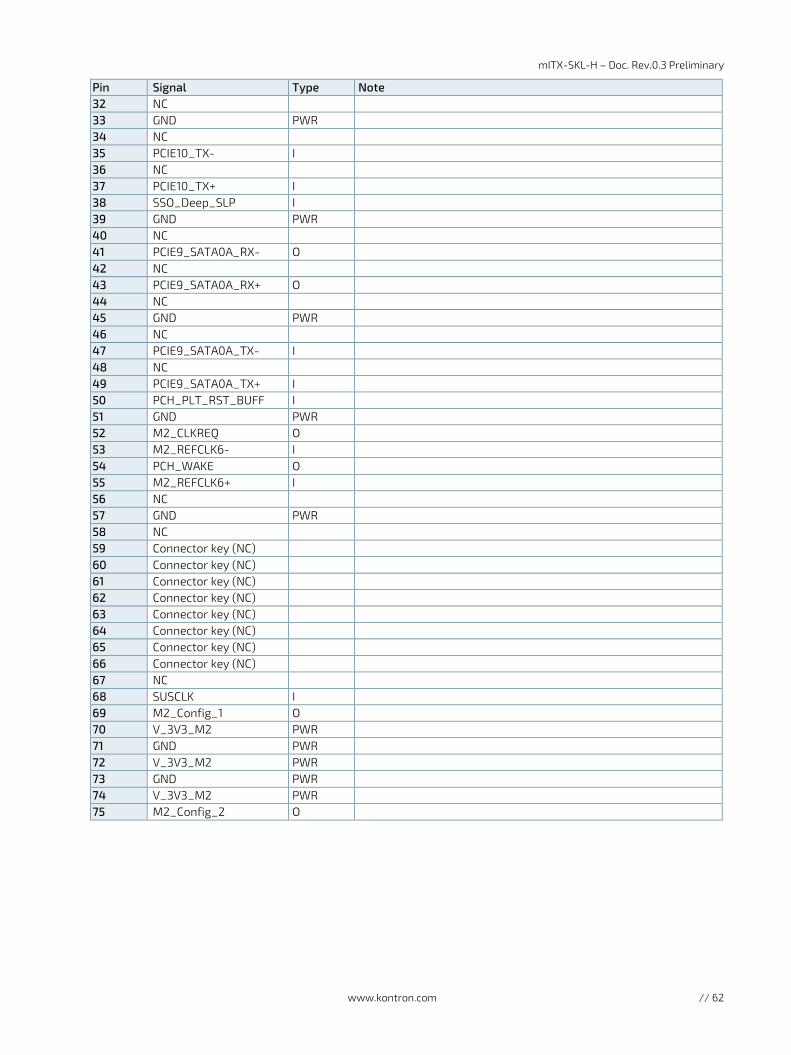
mITX-SKL-H – Doc. Rev.0.3 Preliminary
www.kontron.com // 62
Pin Signal Type Note 32 NC 33 GND PWR 34 NC 35 PCIE10_TX- I 36 NC 37 PCIE10_TX+ I 38 SSO_Deep_SLP I 39 GND PWR 40 NC 41 PCIE9_SATA0A_RX- O 42 NC 43 PCIE9_SATA0A_RX+ O 44 NC 45 GND PWR 46 NC 47 PCIE9_SATA0A_TX- I 48 NC 49 PCIE9_SATA0A_TX+ I 50 PCH_PLT_RST_BUFF I 51 GND PWR 52 M2_CLKREQ O 53 M2_REFCLK6- I 54 PCH_WAKE O 55 M2_REFCLK6+ I 56 NC 57 GND PWR 58 NC 59 Connector key (NC) 60 Connector key (NC) 61 Connector key (NC) 62 Connector key (NC) 63 Connector key (NC) 64 Connector key (NC) 65 Connector key (NC) 66 Connector key (NC) 67 NC 68 SUSCLK I 69 M2_Config_1 O 70 V_3V3_M2 PWR 71 GND PWR 72 V_3V3_M2 PWR 73 GND PWR 74 V_3V3_M2 PWR 75 M2_Config_2 O

mITX-SKL-H – Doc. Rev.0.3 Preliminary
www.kontron.com // 63
8/ On-Board Connectors & Mating Connector Types The Mating connectors / Cables are connectors or cable kits that are fitting the On-board connector. The Kontron cable kits marked with “*” are included in the “mITX-SKL-H Cable & Driver Kit” PN 826603.
The following information is under construction and is subject to change.
Table 39: On-Board Connectors, Mating Connector Types
Connector On-Board Connectors Mating Connectors / Cables Manufact. Type no. Manufact. Type no.
FANCPU, FANSYS (J33, J34)
Foxconn HF2704E-M1 AMP 1375820-4 (4-pole) Molex 47053-1000 AMP 1375820-3 (3-pole)
SATA 1, 2, 3, 4 (J10, J12, J11, J13)
Lotes ABA-SAT-010-K08 Molex 67489-8005 Kontron 821035 (kit)
SATA Power 1,2 (J23, J24)
Molex 22-23-2041 Molex 22-01-2045 TE Connectivity 640456-4 TE Connectivity 1375820-4
ATX +12V -4p (J31) Molex 39-28-1043 Molex 39-01-2045 Foxconn HM3502E Lotes ABA-POW-003-K04
DC Jack (J32) Singatron 2DC1003-010111 Headphone (J29) Molex 53047-0410 Molex 51021-0400 LVDS (J7) Samtec SHF-120-01-L-D-SM-K-
TR Kontron 910000005
Pinrex 53C-90-40GBE0 Kontron 821515 (kit) * Kontron 821155 (kit)
COM 1,(J22) Foxconn HL2205F Molex 90635-1103 Pinrex 510-90-10GB00 Kontron 821016 (kit) Cen Link ZP91-014B1-10Y1 Kontron 821017 (kit) *
COM 2 (J35) JST B5B-PH-K-S(LF)(SN)(P) JST PHR-5 USB 2.0 (J27, FRONTPNL) (See FRONTPNL) Kontron 821401 (kit) USB 3.0 (J3) Foxconn HLL2107-CBC2D-4H SPI Hardflash (J9) Pinrex 210-92-06GB01 SPI GPIO (J36) Molex 53047-0610 Molex 51021-0600 SPDIF –OUT (J30) Molex 53047-0210 Molex 51021-0200 FRONTPNL (J27) Pinrex 510-80-24GB05 Molex 90635-1243
Foxconn HL2112V-P9 Kontron 821042 (kit) * FEATURE (J26) Pinrex 52A-90-44GB00 Don Connex A05c-44-B-G-A-1-G
Molex 87831-4420 Kontron 1052-5885 (kit) *
More than one connector can be listed for each type of on-board connectors even though several types with same fit, form and function are approved and could be used as alternative.
Please also notice that standard connectors like DP, miniPCIe, Audio Jack, Ethernet and USB are not included in the list.

mITX-SKL-H – Doc. Rev.0.3 Preliminary
www.kontron.com // 64
9/ BIOS
9.1. Starting the UEFI BIOS
The mITX-SKL-H is provided with a Kontron-customized, pre-installed and configured version of AMI Aptio ® V UEFI BIOS. AMI BIOS firmware based on the Unified Extensible Firmware Interface (UEFI 2.x) specification and the Intel® Platform Innovation Framework for EFI. This UEFI BIOS provides a variety of new and enhanced functions specifically tailored to the hardware features of the mITX-SKL-H
The UEFI BIOS comes with a Setup program which provides quick and easy access to the individual function settings for control or modification of the UEFI BIOS configuration. The Setup program allows the accessing of various menus which provide functions or access to sub-menus with more specific functions of their own.
To start the UEFI BIOS Setup program, follow the steps below:
1. Power on the board.
2. Wait until the first characters appear on the screen (POST messages or splash screen).
3. Press the <DEL> key.
4. If the UEFI BIOS is password-protected, a request for password will appear. Enter either the User Password or the Supervisor Password (see Security menu), press <RETURN>, and proceed with step 5.
5. A Setup menu will appear.
The mITX-SKL-H UEFI BIOS Setup program uses a hot key-based navigation system. A hot key legend bar is located on the bottom of the Setup screens.
The following table provides information concerning the usage of these hot keys.
Table 40: Navigation
Hotkeys Description
<F1> The <F1> key is used to invoke the General Help window.
<-> The <Minus> key is used to select the next lower value within a field.
<+> The <Plus> key is used to select the next higher value within a field.
<F2> The <F2> key is used to load the previous values.
<F3> The <F3> key is used to load the standard default values.
<F4> The <F4> key is used to save the current settings and exit the UEFI BIOS Setup.
<→> or <←> The <Left/Right> arrows are used to select major Setup menus on the menu bar. For example: Main screen, Advanced screen, Security screen, etc.
<↑> or <↓> The <Up/Down> arrows are used to select fields in the current menu. For example: A Setup function or a sub-screen.
<ESC> The <ESC> key is used to exit a major Setup menu and enter the Exit Setup menu. Pressing the <ESC> key in a sub-menu causes the next higher menu level to be displayed.
<RETURN> The <RETURN> key is used to execute a command or select a submenu.

mITX-SKL-H – Doc. Rev.0.3 Preliminary
www.kontron.com // 65
9.2. Setup Menus
The Setup utility features four menus listed in the selection bar at the top of the screen:
Main Advanced Chipset Security Boot Save & Exit
The Setup menus are selected via the left and right arrow keys. The currently active menu and the currently active UEFI BIOS Setup item are highlighted in white. Each Setup menu provides two main frames. The left frame displays all available functions. Functions that can be configured are displayed in blue. Functions displayed in gray provide information about the status or the operational configuration. The right frame displays an Item Specific Help window providing an explanation of the respective function.
The setup menus are under construction. The following sections explain what type of information will be included in each setup menu.
9.2.1. Main Setup Menu Upon entering the UEFI BIOS Setup program, the Main Setup menu is displayed. This screen lists the Main Setup menu sub-screens and provides basic system information as well as functions for setting the system time and date.
Table 41: Main Setup Menu Sub-Screens and Functions
Sub-screen Description Board Information Read only field
Displays information about the Board Board ID, Fab ID and LAN PHY Revision
Processor Information Read only field Displays information about the CPU, BIOS and Memory Name, Type, Frequency, Processor ID, Stepping, Package, Number of Processors, Microcode Version, GT Info, VBIOS Version, GOP Version, Total memory and Memory Frequency
PCH Information Read only field Displays information about the PCH Name, PCH SKU, Stepping, Hsio Revision, Package, TXT Capability Platform/PCH, ProductionType, Dual Output Fast, Read Support, Read ID Status Clock Frequency, Write and Erase, Clock Frequency, Fast Read Status Clock Frequency, Fast Read Support, Read clock frequency, number of components, SPI Components, Density, Firmware revision, Firmware SKU
System Language Selects system language System Date Displays system date System Time Displays system time
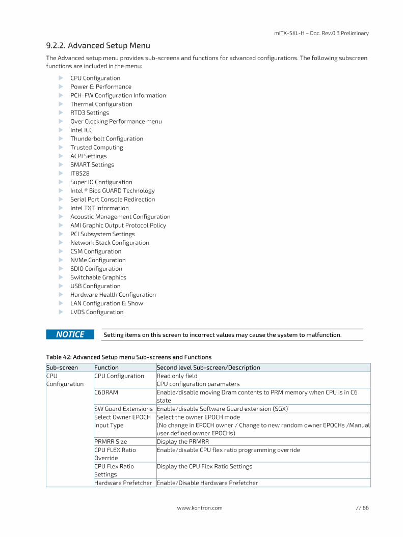
mITX-SKL-H – Doc. Rev.0.3 Preliminary
www.kontron.com // 66
9.2.2. Advanced Setup Menu The Advanced setup menu provides sub-screens and functions for advanced configurations. The following subscreen functions are included in the menu:
CPU Configuration Power & Performance PCH-FW Configuration Information Thermal Configuration RTD3 Settings Over Clocking Performance menu Intel ICC Thunderbolt Configuration Trusted Computing ACPI Settings SMART Settings IT8528 Super IO Configuration Intel ® Bios GUARD Technology Serial Port Console Redirection Intel TXT Information Acoustic Management Configuration AMI Graphic Output Protocol Policy PCI Subsystem Settings Network Stack Configuration CSM Configuration NVMe Configuration SDIO Configuration Switchable Graphics USB Configuration Hardware Health Configuration LAN Configuration & Show LVDS Configuration
Setting items on this screen to incorrect values may cause the system to malfunction.
Table 42: Advanced Setup menu Sub-screens and Functions
Sub-screen Function Second level Sub-screen/Description CPU Configuration
CPU Configuration Read only field CPU configuration paramaters
C6DRAM Enable/disable moving Dram contents to PRM memory when CPU is in C6 state
SW Guard Extensions Enable/disable Software Guard extension (SGX) Select Owner EPOCH Input Type
Select the owner EPOCH mode (No change in EPOCH owner / Change to new random owner EPOCHs /Manual user defined owner EPOCHs)
PRMRR Size Display the PRMRR CPU FLEX Ratio Override
Enable/disable CPU flex ratio programming override
CPU Flex Ratio Settings
Display the CPU Flex Ratio Settings
Hardware Prefetcher Enable/Disable Hardware Prefetcher

mITX-SKL-H – Doc. Rev.0.3 Preliminary
www.kontron.com // 67
Sub-screen Function Second level Sub-screen/Description Attach Cache Line Prefetcher
Turns on/off adjacent cache lines prefetching
Intel (VMX) Virtualization Technology
Enable/disable Intel (VMX) to use additional hardware capabilities provided by Vanderpool Technology
PECI Enable/disable PECI Active Processor Cores
Display number of cores to enable in each processor package
Hyper Threading Enable/disable OS optimized Hyper-Threading technology Enable – Windows XP and Linux / Disable - other OS
BIST Enable/disable built-in self-test (BIST) on request JTAG C10 Power Enable/disable power JTAG in C10 and deeper power states AP Threads IDLE Manner
AP threads idle manner for waiting signal to run
AP Threads Handoff Manner
AP treads handoff to OS manner from end of post
AES Enable/disable Advanced Encryption Standard (AES) Machine Check Enable/disable machine check MonitorMWait
Enable/disable MonitorMWait
Intel Trusted Execution Technology
Enable/disable utilization of additional hardware capabilities provided by Intel® Trusted Execution technology Note: Changes require a full power cycle to take effect.
Alias Check Request DPR Memory Size (MB)
Display Alias Check Request DPR Memory Size (MB)
Reset AUX Content Reset TPM Aux content Note TXT may not be functional after AUX content is reset.
Flash Wear-Out Protection
Enable/disable flash wear-out protection feature
Current Debug Interface Status
Display Current Debug Interface Status
Debug Interface Enable/disable debug interface support Debug Interface lock Enable/disable debug interface lock Processor Trace Memory Allocation
Select or disable processor trace memory region size (Range 4 KB- 128 MB)
CPU SMM Enhancement
SMM Code Access Check
Enable/Disable support for SMM Code Access feature
SMM Use Delay Indication
Enable/Disable usage of SMM_DELAYED MSR for MP sync in SMI
SMM Use Block Indication
Enable/Disable usage of SMM_BLOCKED MSR for MP sync in SMI
FCLK Frequency for Early Power-On
Select EFCLK frequency values (400 MHz, 800 MHz, 1 GHz)
Voltage Optimization Select voltage optimization option Enable/disable/auto Power & Performance
CPU – Power Management Control
Boot Performance Mode
Select performance state set by BIOS, starting from reset vector
Intel ® Speedstep™
Enable /disable support for more than two frequency ranges
Race to Halt (RTH)
Enable/disable race to halt feature Note: RTH feature dynamically increases CPU frequency to enter pkg C-state faster to reduce overall power. RTH is controlled through MSR.

mITX-SKL-H – Doc. Rev.0.3 Preliminary
www.kontron.com // 68
Sub-screen Function Second level Sub-screen/Description Intel® Speed Shift™ Technology
Enable/disable Intel®speed shift™ technology support for P-state hardware control by exposing CPPC v2 interface.
HDC Control Enable/disable HDC configuration Note: can be enable by OS if OS native support available
Turbo Mode Enable/disable processor turbo mode if EMTMM is also enabled. Auto-enabled unless max. turbo ratio is bigger than 16
View/Configure Turbo Options
Energy Efficient P-State
Enable/disable Energy Efficient P-State feature
Package Power Limit MSR Lock
Enable/disable locking of Package Power Limit
1-Core Ratio Limit Override
Display 1-Core Ratio Limit Override
2-Core Ratio Limit Override
Display 2-Core Ratio Limit Override
3-Core Ratio Limit Override
Display 3-Core Ratio Limit Override
4-Core Ratio Limit Override
Display 4-Core Ratio Limit Override
Energy Efficient Turbo
Enable/disable Energy Efficient Turbo Feature
Config TDP Configuration
Configurable TDP Boot Mode
Configurable TDP Mode as Nominal/Up/Down/Deactivate TDP selection
Configurable TDP Lock
Enable/disable Configurable TDP Lock
CTDP BIOS Control
Enable/disable CTDP Control via runtime ACPI BIOS methods
ConfigTDP Levels
ConfigTDP Turbo Activation Ratio, Power Limit 1, Power Limit 2
Custom Settings Nominal ConfigTDP Nominal
Setting for Power Limit 1, Power Limit 2, Power Limit 1 Time Window, ConfigTDP Turbo Activation Ratio
Custom Settings Down ConfigTDP Level 1 and 2
CPU VR Settings PSYS Slope Display PSYS slope in 1 /100 increments (Range: 0-200)
PSYS Offset Display PSYS slope in 1 /4 increments (Range: 0-200)
PSYS Pmax Power
Display PSYS Power defined in 1/8 Watt increments (Range: 0-8192)
Acoustic Noise Settings
Acoustic Noise Mitigation
Enable/disable Acoustic Noise Mitigation
IA VR Domain Display disable Fast PKG C State Ramp for IA Domain and Slow Slew Rate for IA Domain
GT VR Domain Display disable Fast PKG C State Ramp for GT Domain and Slow Slew Rate for GT Domain

mITX-SKL-H – Doc. Rev.0.3 Preliminary
www.kontron.com // 69
Sub-screen Function Second level Sub-screen/Description SA VR Domain Display disable Fast PKG
C State Ramp for SA Domain and Slow Slew Rate for SA Domain
Core/IA VR Settings GT-Unsliced VR Settings GT Sliced VR Settings
VR Config enable AC Loadline DC Load Line PS Current Threshold 1 / 2 / 3 PS3 Enable PS4 Enable IMON Slope IMON Offset IMON Prefix VR Current Limit VR Voltage Limit TDC Enable TDC Current Limit TDC Time Window TDC Lock
VR Mailbox Command Options
Display VR Mailbox Command options 1: MPS VR Command 2: PS4 Exit VR command 4: MPS VR decay command Note: Multiple commands can be selected by entering sum from values of each command.
Platform PL1 Enable
Enable/disable perform power limit 1 programming by activating PL1 value used by processor to limit given power
Platform PL2 Enable
Enable/disable perform power limit 2 programming. If disabled, BIOS programs the default values for Platform power limit 2.
Power Limit 4 Override
Enable/disable power limit 4 override. If disabled, BIOS leaves default values for power limit 4
C-State Enable/disable CPU power management CPU to enter C-state when not 100 % utilized
Enhanced C-State
Enable/disable C11E If all cores enter C-state, CPU switches to min. speed.
C-State Auto Demotion
Configure C-state auto demotion
C-State Undemotion
Configure C-state undemotion
Package C-State Demotion
Enable /disable Package C-state demotion
Package C-state Undemotion
Enable/disable Package C-state undemotion
C-State Prewake Enable/disable C-state prewake Disable by setting bit 30 of POWER_CTL MSR (0X1FC) to 1
IO MWait Redirection
If set, maps IO_read instructions sent to IO registers PMG_IO_BASE_ADDRBASE+off set to MWAIT(offset)
Package C-state Limit
Select the maximum package C-state limit setting

mITX-SKL-H – Doc. Rev.0.3 Preliminary
www.kontron.com // 70
Sub-screen Function Second level Sub-screen/Description C3 Latency Control (MSR 0x60A) C6/C7 Short Latency Control (MSR 0X60B) C6/C7 Long Latency Control (MSR 0X60C)
Setting of time unit (Unit of measurement for IRTL value) and Latency Setting of time unit (Unit of measurement for IRTL value) and Latency
Thermal Monitor Enable/disable thermal monitoring Interrupt Redirection Mode
Select interrupt redirect mode for interrupt redirection
Timed Mwait Enable /disable timed MWAIT support Custom P-State Table
Number of P-States
Display number of custom P-states Note: Minimum of 2 states must be present.
Energy Performance Gain
Enable/disable energy performance gain
Power Limit 3 Settings
Power Limit 3 Override
Enable/disable power limit 3 override If disabled, BIOS leaves the default values for power limit 3 and power limit 3 time window.
CPU Lock Configuration
CFG Lock Enable/ disable configuration of 0XE2[15] CFG lock bit
Over Clocking Lock
Enable/disable overclocking lock bit 20 in FLEX ratio (194) MSR
GT- Power Management Control
RC6 ( Render Standby) Check to enable render standby support
Maximum GT Frequency
Choose between 350MHz (RPN) and 1000MHz (RPO). Value beyond the range will be clipped to min/max supported by SKU
PCH-FW Configuration Information
ME Firmware Version Display ME Firmware Version ME Firmware Mode Display ME Firmware Mode ME Firmware SKU Display ME Firmware SKU ME File System Integrity Value
Display ME File System Integrity Value
ME Firmware Status 1 Display ME Firmware Status 1 ME Firmware Status 2 Display ME Firmware Status 2 NFC Support Display NFC Support ME State Enable/disable ME temporary disabled mode Manageability Features State
Display Manageability Enable/disable manageability features supported in firmware
Features State Display Features State AMT BIOS Features Enable/disable AMT BIOS feature support
If not supported the user is no longer able to access MEBx. Note: This option does not disable manageability.
AMT Configuration ASF support Enable/disable Alert Standard Format Support
USB Provisioning of AMT Enable/disable of AMT USB Provisioning
CIRA Configuration
Active Remote Assistance Process
Trigger CIRA boot
CIRA Timeout Display CIRA Timeout

mITX-SKL-H – Doc. Rev.0.3 Preliminary
www.kontron.com // 71
Sub-screen Function Second level Sub-screen/Description ASF Configuration PET Progress Enable/disable PET Events Progress to
receive PET Events Watchdog Enable/disable Watchdog Timer OS Timer Display OS Timer BIOS Timer Display BIOS Timer
Secure Erase Configuration
Secure Erase Mode Change Secure Erase module behavior Force Secure Erase Force Secure Erase on next boot
OEM Flags Settings
MEBx hotkey Pressed
Enable/disable MEBx hotkey Pressed
MEBx Selection Screen
Enable/disable MEBx Selection Screen
Hide Unconfigure ME Confirmation Prompt
Enable/disable Hide Unconfigure ME Confirmation Prompt
MEBx OEM Debug Menu Enable
Enable/disable MEBx OEM Debug Menu
Unconfigure ME Enable/disable Unconfigure ME MEBx Resolution Settings
Non-UI Mode Resolution
Resolution for non-UI text mode
UI Mode Resolution
Resolution for UI text mode
Graphic Mode Resolution
Resolution for graphics mode
ME Unconfig O RTC clear
Display ME Unconfig on RTC Clear
Comms Hub Support Enable/disable support for comms hub JHI Support Enable/disable Intel® DAL Host Interface service (JHI) Core BIOS Done Message
Enable/disable sending core BIOS done message to ME
Firmware Update Configuration
ME FW Image Re-Flash Enable/disable ME FW Image re-flash function
PTT Configuration PTT Capability/State Display PTT Capability/State TPM Device Selection Select TPM device: PTT or dTPM. PTP Aware OS Display PTP aware OS
ME Debug Configuration
HECI Timeouts Enable/disable HECI Send/Receive Timeouts Force ME DID Init Status Force the DID Initialization Status value CPU Replaced Polling Disable Setting this option disables CPU replacement
polling loop ME DID Message Enable/disable ME DID Message HECI Retry Disable Setting this option disables retry mechanism
for all HECI APIs HECI Message check Disable Setting this option disables message check for
Bios Boot Path when sending MBP HOB Skip Setting this option skips MBP HOB HECI2 Interface Communication
Adds and removes HECI2 Device from PCI space
KT Device Enable/disable KT Device IDER Device Enable/disable IDER Device End Of Post Message Enable/disable End Of Post Message sent to
ME DOI3 Setting for HECI Disable Setting this option disables setting DOI3 bit for
all HECI devices Note: This menu is for testing purposes. It is recommended to leave the options in their default states.

mITX-SKL-H – Doc. Rev.0.3 Preliminary
www.kontron.com // 72
Sub-screen Function Second level Sub-screen/Description Thermal Configuration
CPU Thermal Configuration
DTS SMM Enable/disable DTS SMM TCC Activation Offset
Offset from factory set Tcc activation temperature at which the Thermal Control Circuit must be activated. Note: TCC activated at: TCC activation temp / TCC activation offset.
TCC Offset Time Window
Enable/disable TCC offset time window for running average temperature limits (RATL) feature (Range:5 ms to 448 s)
TCC Offset Clamp Enable
Enable/disable running average temperature limit (RATL) feature to allow CPU to throttle below P1
TCC Offset Lock Enable
Enable/disable lock for running average temperature limit (RATL) feature to lock temperature target MSR
Bi-directional PROCHOT#
Enable/disable Bi-directional PROCHOT#
Disable PROCHOT# Output
Enable/disable PROCHOT# output
Disable VR Thermal Alert
Enable/disable VR thermal alert
PROCHOT Response
Enable/disable PPROCHOT response
PROCHOT Lock Enable/disable PPROCHOT lock ACPI T-State Enable/disable PACPI T-state
Platform Thermal Configuration
Automatic Thermal Reporting
Configure _CRT, _PSV and _ACO automatically based on values recommended in BWG’s thermal reporting for thermal management settings.
Critical Trip Point
Control temperature value at the ACPI critical trip point at which OS shuts off the system. Note :119 is the plan of record (POR)
Active Trip Point 0
Display temperature value at the ACPI Active trip point 0 at which OS turns on the processor fan.
Active Trip Point 0 Fan Speed
Active Trip Point 1 Fan Speed in percentage (Range: O %= fan off, 100 % = fan speed maximum)
Active Trip Point 1
This value controls the temperature of the ACPI Active Trip Point 1
Active Trip Point 1 Fan Speed
Active Trip Point 1 Fan Speed in percentage (Range: O %= fan off, 100 % = fan speed maximum)
Passive Trip Point
This value controls the temperature of the ACPI Passive Trip Point, point at which OS starts to throttle processor
Passive TC1 Value Sets TC1 or TC2 value for the ACPI passive cooling formula (Range: 1-16) Passive TC2 Value
Passive TSP Value Set TSP value for the ACPI passive cooling formula Active Trip Points Enable/disable active trip points Passive Trip Points Enable/disable passive trip points Critical Trip Pints Enable/disable critical trip points PCH Thermal Device
Enable/disable PCH thermal device (D20:F2)
PCH Temp Read Enable/disable PCH temperature read CPU Energy Read Enable/disable CPU energy read CPU Temp Read Enable/disable CPU temperature read Alert Enable lock Enable/disable alert enable lock CPU Temp Fail safe temperature that EC uses if OS hangs CPU Fan Speed Fan speed that EC uses if OS hangs
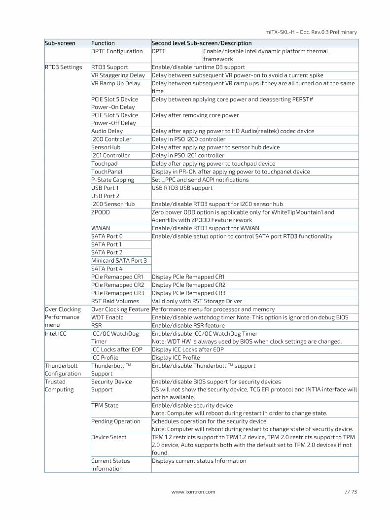
mITX-SKL-H – Doc. Rev.0.3 Preliminary
www.kontron.com // 73
Sub-screen Function Second level Sub-screen/Description DPTF Configuration DPTF Enable/disable Intel dynamic platform thermal
framework RTD3 Settings RTD3 Support Enable/disable runtime D3 support
VR Staggering Delay Delay between subsequent VR power-on to avoid a current spike VR Ramp Up Delay Delay between subsequent VR ramp ups if they are all turned on at the same
time PCIE Slot 5 Device Power-On Delay
Delay between applying core power and deasserting PERST#
PCIE Slot 5 Device Power-Off Delay
Delay after removing core power
Audio Delay Delay after applying power to HD Audio(realtek) codec device I2CO Controller Delay in PSO I2C0 controller SensorHub Delay after applying power to sensor hub device I2C1 Controller Delay in PSO I2C1 controller Touchpad Delay after applying power to touchpad device TouchPanel Display in PR-ON after applying power to touchpanel device P-State Capping Set _PPC and send ACPI notifications USB Port 1 USB RTD3 USB support USB Port 2 I2C0 Sensor Hub Enable/disable RTD3 support for I2C0 sensor hub ZPODD Zero power ODD option is applicable only for WhiteTipMountain1 and
AdenHills with ZPODD Feature rework WWAN Enable/disable RTD3 support for WWAN SATA Port 0 Enable/disable setup option to control SATA port RTD3 functionality SATA Port 1 SATA Port 2 Minicard SATA Port 3 SATA Port 4 PCIe Remapped CR1 Display PCIe Remapped CR1 PCIe Remapped CR2 Display PCIe Remapped CR2 PCIe Remapped CR3 Display PCIe Remapped CR3 RST Raid Volumes Valid only with RST Storage Driver
Over Clocking Performance menu
Over Clocking Feature Performance menu for processor and memory WDT Enable Enable/disable watchdog timer Note: This option is ignored on debug BIOS RSR Enable/disable RSR feature
Intel ICC ICC/OC WatchDog Timer
Enable/disable ICC/OC WatchDog Timer Note: WDT HW is always used by BIOS when clock settings are changed.
ICC Locks after EOP Display ICC Locks after EOP ICC Profile Display ICC Profile
Thunderbolt Configuration
Thunderbolt ™ Support
Enable/disable Thunderbolt ™ support
Trusted Computing
Security Device Support
Enable/disable BIOS support for security devices OS will not show the security device, TCG EFI protocol and INT1A interface will not be available.
TPM State Enable/disable security device Note: Computer will reboot during restart in order to change state.
Pending Operation Schedules operation for the security device Note: Computer will reboot during restart to change state of security device.
Device Select TPM 1.2 restricts support to TPM 1.2 device, TPM 2.0 restricts support to TPM 2.0 device, Auto supports both with the default set to TPM 2.0 devices if not found.
Current Status Information
Displays current status Information

mITX-SKL-H – Doc. Rev.0.3 Preliminary
www.kontron.com // 74
Sub-screen Function Second level Sub-screen/Description ACPI Settings Enable ACPI Auto
Configuration Enable/disable BIOS ACPI auto configuration
Enable Hibernation Enable/Disable systems ability to Hibernate (OS/S4 sleep state) Note: This option may not be effective with some OS(s).
ACPI Sleep State Selects highest ACPI sleep state system enters when SUSPEND is pressed Lock Legacy Resources
Enable/disable lock of legacy resources
S3 Video Repost Enable/disable S3 video repost SMART Settings Smart Self-Test Enable/disable running smart self-test on all HDDs during POST IT8528 Super IO Configuration
Super IO Chip IT8528 Serial Port 1 Configuration
Serial Port Enable/disable Serial Port (COM) Device Settings Display device settings Change Settings Select an optimal settings for Super IO
Device Serial Port 2 Configuration
Serial Port Enable/disable Serial Port (COM) Device Settings Display device settings Change Settings Select an optimal settings for Super IO
Device RS422 Duplex Mode Set full or half duplex mode RTS Control Select receiver controlled RTS Enable
or permanently enable RTS Intel ® Bios GUARD Technologcy
Intel ® Bios Guard Support
Enable/disable Intel BIOS guard support
Serial Port Console Redirection
Console Redirection Enable/disable console redirection Control Redirection Settings
Terminal Type Emulation: ANSI: Extended ASCII char set. VT100: ASCII char set. VT100+: Extends VT100 to support color, function keys, etc. VT-UTF8: Uses UTF8 encoding to map Unicode
Bits per second Select serial port transmission speed Data Bits Data Bits Parity A parity bit can be sent with the data bit to detect some
transmission errors Stop Bits Stops bits indicate the end of a serial data packet Flow Control Flow control can prevent data loss from buffer overflow VT-UTF8 Combo Key Support
Enable VT-UTF8 Combination Key Support for ANSI/VT100 terminals
Recorder Mode With this mode enabled only text will be sent. This is to capture terminal data
Resolution 100x31
Enable/disabled extended terminal resolution
Legacy OS Redirection Resolution
On Legacy OS, the number of rows and columns supported redirection.
Putty KeyPad Select function key and keypad on Putty.
Redirection After BIOS POST
The settings specify if bootLoader is selected then Legacy console redirection is disable before booting to Legacy OS
COM1(Pci Bus0, Dev0, Func0) Read only field Console Redirection Read Only field - Port is disable Legacy Control Redirection settings
Legacy Serial Redirection Port
Selects a COM port to display redirection of legacy OPROM messages

mITX-SKL-H – Doc. Rev.0.3 Preliminary
www.kontron.com // 75
Sub-screen Function Second level Sub-screen/Description Serial Port for Out-of-Band Management /Windows Emergency Management Services Console Redirection
Enable/disable Console Redirection
Intel TXT Information
Chipset Read Only field - Production Fused BiosAcm Read Only field - Production Fused Chipset Txt Read Only field - Supported Cpu Txt Read Only field - Supported Error Code Read Only field - None Class Code Read Only field - None Major Code Read Only field - None Minor Code Read Only field – None
Acoustic Management Configuration
Read only field HDD not found
AMI Graphic Output Protocol Policy
Output Select Output Interface Brightness Setting Read only field BIST enable Read only field
PCI Subsystem Settings
AMI PCI Driver Version Read only field - A5.01.11 Above 4G Decoding Enable/disable Above 4G Decoding Hot-Plug Support Hot-Plug Support Restore PCIE Registers
Enable/disable Restore PCIE Registers
Don’t Reset VC-TC Mapping
Enable/disable Don’t Reset VC-TC Mapping
Network Stack Configuration
Network Stack Enable/disable UEFI network stack
CSM Configuration
CSM support Enable/disable Compatibility Support Module support
NVMe Configuration
NVMe controller and Device information
No NVMe Device Found
SDIO Configuration
SDIO Access Mode Auto Option: Access SD device in DMA mode if controller supports it, otherwise in PIO mode
Switchable Graphics
SG Mode Select Read only field muxless
USB Configuration
Legacy USB Support Enables Legacy USB support XHCI Hand-off Workaround for OS(s) without XHCI hand-off support USB Mass Storage Driver Support
Enable/disable USB Mass Storage Driver Support
Port 60/64 Emulation Enable/disable Port 60/64 Emulation USB transfer time-out Time-out value for Control, Bulk, and Interrupt transfer Device reset time-out USB mass storage device start unit command time-out Device power-up delay
Maximum time the device takes before the device reports itself to the Host Controller properly.
Hardware Health Configuration
System Temperature Display the System Temperature
System Temperature Offset
Adjust the offset value in C (Two’s Complement)
CPU Temperature Display CPU Temperature System Fan Speed Display System Fan Speed System Fan Cruise Control
Disable = Full speed Thermal = does regulate fan speed according to specified temperature Speed = does regulate according to specified speed
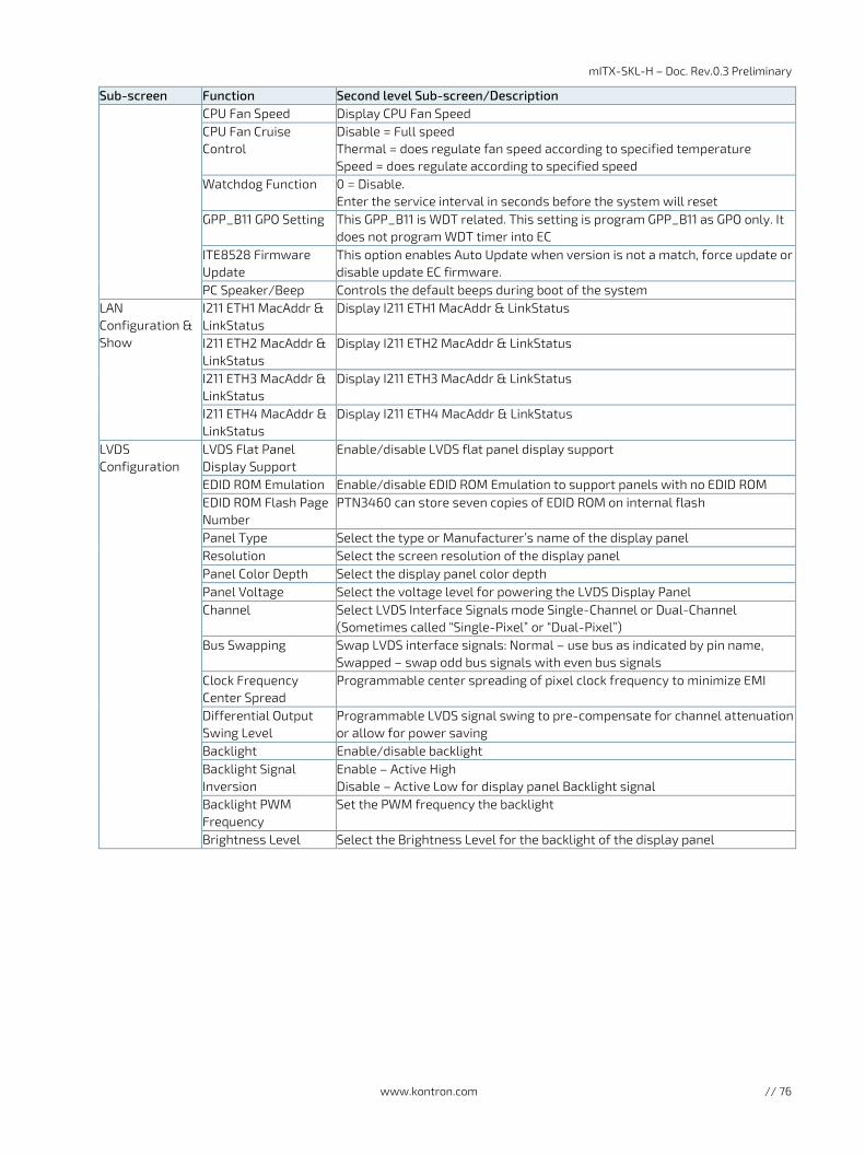
mITX-SKL-H – Doc. Rev.0.3 Preliminary
www.kontron.com // 76
Sub-screen Function Second level Sub-screen/Description CPU Fan Speed Display CPU Fan Speed CPU Fan Cruise Control
Disable = Full speed Thermal = does regulate fan speed according to specified temperature Speed = does regulate according to specified speed
Watchdog Function 0 = Disable. Enter the service interval in seconds before the system will reset
GPP_B11 GPO Setting This GPP_B11 is WDT related. This setting is program GPP_B11 as GPO only. It does not program WDT timer into EC
ITE8528 Firmware Update
This option enables Auto Update when version is not a match, force update or disable update EC firmware.
PC Speaker/Beep Controls the default beeps during boot of the system LAN Configuration & Show
I211 ETH1 MacAddr & LinkStatus
Display I211 ETH1 MacAddr & LinkStatus
I211 ETH2 MacAddr & LinkStatus
Display I211 ETH2 MacAddr & LinkStatus
I211 ETH3 MacAddr & LinkStatus
Display I211 ETH3 MacAddr & LinkStatus
I211 ETH4 MacAddr & LinkStatus
Display I211 ETH4 MacAddr & LinkStatus
LVDS Configuration
LVDS Flat Panel Display Support
Enable/disable LVDS flat panel display support
EDID ROM Emulation Enable/disable EDID ROM Emulation to support panels with no EDID ROM EDID ROM Flash Page Number
PTN3460 can store seven copies of EDID ROM on internal flash
Panel Type Select the type or Manufacturer’s name of the display panel Resolution Select the screen resolution of the display panel Panel Color Depth Select the display panel color depth Panel Voltage Select the voltage level for powering the LVDS Display Panel Channel Select LVDS Interface Signals mode Single-Channel or Dual-Channel
(Sometimes called “Single-Pixel” or “Dual-Pixel”) Bus Swapping Swap LVDS interface signals: Normal – use bus as indicated by pin name,
Swapped – swap odd bus signals with even bus signals Clock Frequency Center Spread
Programmable center spreading of pixel clock frequency to minimize EMI
Differential Output Swing Level
Programmable LVDS signal swing to pre-compensate for channel attenuation or allow for power saving
Backlight Enable/disable backlight Backlight Signal Inversion
Enable – Active High Disable – Active Low for display panel Backlight signal
Backlight PWM Frequency
Set the PWM frequency the backlight
Brightness Level Select the Brightness Level for the backlight of the display panel
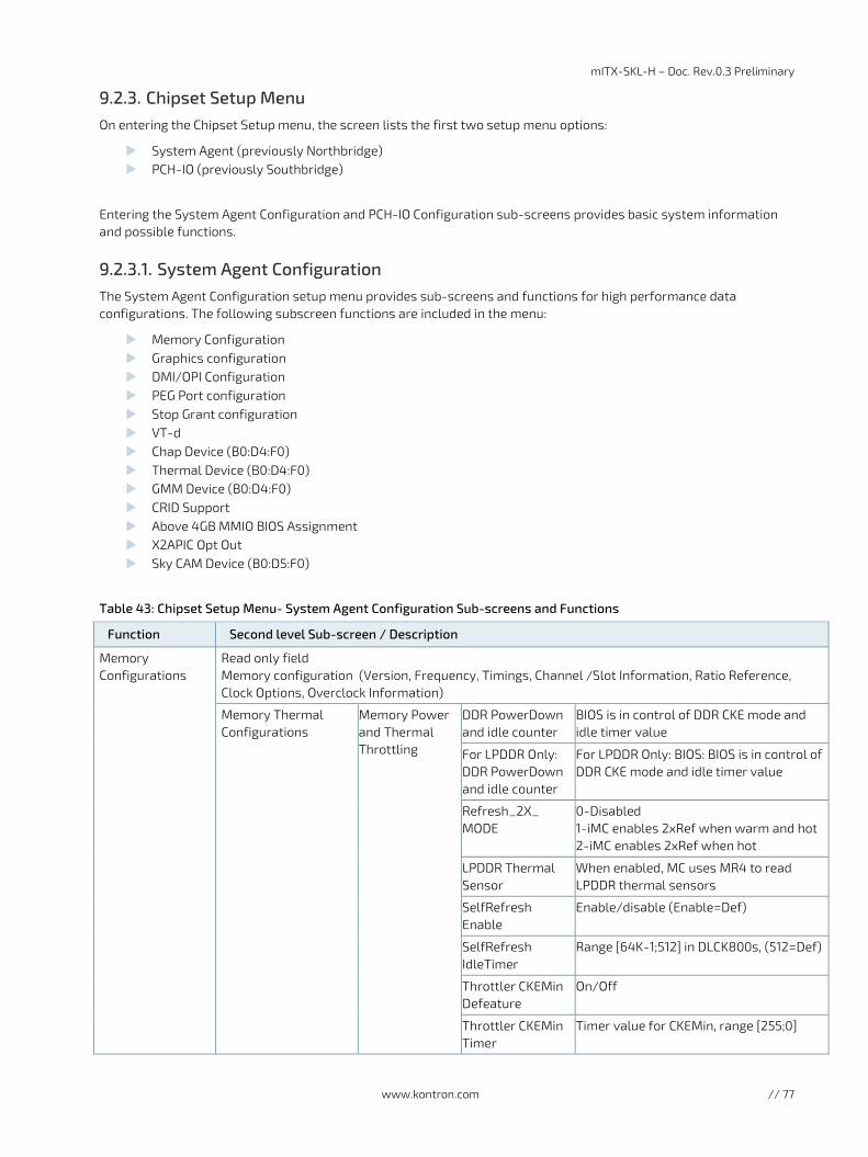
mITX-SKL-H – Doc. Rev.0.3 Preliminary
www.kontron.com // 77
9.2.3. Chipset Setup Menu On entering the Chipset Setup menu, the screen lists the first two setup menu options:
System Agent (previously Northbridge) PCH-IO (previously Southbridge)
Entering the System Agent Configuration and PCH-IO Configuration sub-screens provides basic system information and possible functions.
9.2.3.1. System Agent Configuration The System Agent Configuration setup menu provides sub-screens and functions for high performance data configurations. The following subscreen functions are included in the menu:
Memory Configuration Graphics configuration DMI/OPI Configuration PEG Port configuration Stop Grant configuration VT-d Chap Device (B0:D4:F0) Thermal Device (B0:D4:F0) GMM Device (B0:D4:F0) CRID Support Above 4GB MMIO BIOS Assignment X2APIC Opt Out Sky CAM Device (B0:D5:F0)
Table 43: Chipset Setup Menu- System Agent Configuration Sub-screens and Functions
Function Second level Sub-screen / Description
Memory Configurations
Read only field Memory configuration (Version, Frequency, Timings, Channel /Slot Information, Ratio Reference, Clock Options, Overclock Information)
Memory Thermal Configurations
Memory Power and Thermal Throttling
DDR PowerDown and idle counter
BIOS is in control of DDR CKE mode and idle timer value
For LPDDR Only: DDR PowerDown and idle counter
For LPDDR Only: BIOS: BIOS is in control of DDR CKE mode and idle timer value
Refresh_2X_ MODE
0-Disabled 1-iMC enables 2xRef when warm and hot 2-iMC enables 2xRef when hot
LPDDR Thermal Sensor
When enabled, MC uses MR4 to read LPDDR thermal sensors
SelfRefresh Enable
Enable/disable (Enable=Def)
SelfRefresh IdleTimer
Range [64K-1;512] in DLCK800s, (512=Def)
Throttler CKEMin Defeature
On/Off
Throttler CKEMin Timer
Timer value for CKEMin, range [255;0]
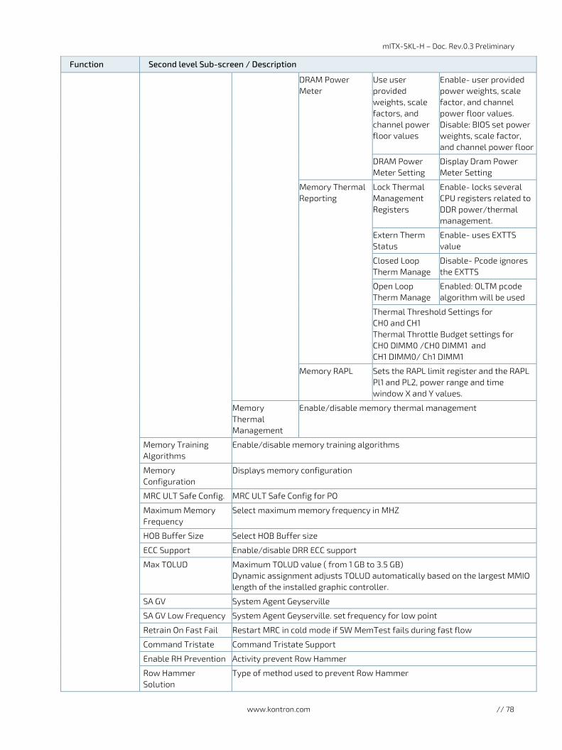
mITX-SKL-H – Doc. Rev.0.3 Preliminary
www.kontron.com // 78
Function Second level Sub-screen / Description
DRAM Power Meter
Use user provided weights, scale factors, and channel power floor values
Enable- user provided power weights, scale factor, and channel power floor values. Disable: BIOS set power weights, scale factor, and channel power floor
DRAM Power Meter Setting
Display Dram Power Meter Setting
Memory Thermal Reporting
Lock Thermal Management Registers
Enable- locks several CPU registers related to DDR power/thermal management.
Extern Therm Status
Enable- uses EXTTS value
Closed Loop Therm Manage
Disable- Pcode ignores the EXTTS
Open Loop Therm Manage
Enabled: OLTM pcode algorithm will be used
Thermal Threshold Settings for CH0 and CH1 Thermal Throttle Budget settings for CH0 DIMM0 /CH0 DIMM1 and CH1 DIMM0/ Ch1 DIMM1
Memory RAPL Sets the RAPL limit register and the RAPL Pl1 and PL2, power range and time window X and Y values.
Memory Thermal Management
Enable/disable memory thermal management
Memory Training Algorithms
Enable/disable memory training algorithms
Memory Configuration
Displays memory configuration
MRC ULT Safe Config. MRC ULT Safe Config for PO
Maximum Memory Frequency
Select maximum memory frequency in MHZ
HOB Buffer Size Select HOB Buffer size
ECC Support Enable/disable DRR ECC support
Max TOLUD Maximum TOLUD value ( from 1 GB to 3.5 GB) Dynamic assignment adjusts TOLUD automatically based on the largest MMIO length of the installed graphic controller.
SA GV System Agent Geyserville
SA GV Low Frequency System Agent Geyserville. set frequency for low point
Retrain On Fast Fail Restart MRC in cold mode if SW MemTest fails during fast flow
Command Tristate Command Tristate Support
Enable RH Prevention Activity prevent Row Hammer
Row Hammer Solution
Type of method used to prevent Row Hammer

mITX-SKL-H – Doc. Rev.0.3 Preliminary
www.kontron.com // 79
Function Second level Sub-screen / Description
RH Activation Probability
Used to adjust MC for Hardware RHP
Exit on Failure (MRC) Exit on Failure for MRC training steps
MC Lock Enable/Disable capacity to lock or not MC registers
Probeless Trace HD Port, GDXC IOT/MOT or Disable
Enable Disable IED (Intel® Enhanced Debug)
Enable/disable Intel® Enhanced debug required 4MB SMM memory
Ch Hash Support Enable/disable channel hash support Note: Only in memory interleave mode
Ch Hash Mask Set the bit(s) included in the XOR function Note: Bit mask corresponds to bits [19:6]
Ch Hash Interleaved Bit
Select the bit used for channel interleave mode Note: Bit 7 interleaves channels at a 2 cache line granularity, (Bit 8 at 4 and Bit 9 at 8).
VC1 Read Metering Enable/disable VC1 Read metering feature (RdMeter)
VC1 RdMeter Time Window
Displays VC1 read metering time window in μs over which VC1 read request counter is tracked
VC1 Rdmeter Threshold
Displays the threshold of the counter in the time window
Strong Weak Leaker Strong weak leaker value
Memory Scrambler Enable/disable memory scrambler
Force Cold Reset Enable/disable force cold reset or mrcColdBoot mode if coldboot is required during MRC execution Note: If ME is 5.0 MB, Force ColdReset is required.
Channel A DIMM Control
Enable/disable DIMMs on channel (either A or B)
Channel B DIMM Control
Force Single Rank If enabled, only Rank 0 will be used in each DIMM
Memory Remap Enable/disable memory remap above 4 GB
Time Measure Enable/disable printing time taken to execute MRC
DLL Weak Lock Support
Enable/disable DLL weak lock support
Pwr Down Idle Timer The minimum value should equal the worst case Roundtrip delay + Burst_Length. 0 means AUTO: 64 for ULX/ULT, 128 for DT/Halo.
MrcFast Boot Enable/disable fast path through the MRC
Lpddr Mem WL Set Sets LPDDR Memory Write Latency (A – default, B- used if memory devices supports the value)
EV Loader Enable/disable EV loader functionality
EV Loader Delay Enable/disable EV loader 2 second delay
Graphics Configuration
Graphics Turbo IMON Current
Displays supported graphics turbo IMON current values (14-31)
Skip Scanned for External GfX Card
Enable - no scan made for external Gfx cards on PEG or PCH PCIE ports.

mITX-SKL-H – Doc. Rev.0.3 Preliminary
www.kontron.com // 80
Function Second level Sub-screen / Description
External Gfx card Primary Display Configuration
Select primary display graphics configuration
Internal Graphics Keeps IGFX enabled, based on setup options
GTT Size Selects GTT size
Aperture Size Selects Aperture size Note: Above 4 GB MMIO, the BIOS assignment is automatically enabled if selecting 2048 MB aperture. To use this feature disable CSM support.
DVMT Pre-Allocated Selects DVMT 5.0 pre-allocated (fixed) graphics memory size used by internal graphics device
DVMT Total Gfx Mem Selects DVMT 5.0 total graphics memory size used by internal graphics device
Gfx Low Power Mode Used for SFF only
VDD Enable Enables/disable VDD forcing in BIOS
HDCP Support Enable/disable HDCP provisioning support
Algorithm Select HDCP re-encryption flow
PM Support Enable/disable PMM support
PAVP Enable Enable/disable PAVP
Cdynmax Clamping Enable
Enable/disable cdynmax clamping
Cd Clock Frequency Select highest Cd clock frequency supported by platform
IUER Button Enable Enable/disable IUER button functionality
DMI/OPI Configuration
DMI Max Link Speed Set DMI maximum Link Speed Gen1 / Gen2 / Gen3 / Auto
DMI Gen 3 EQ Phase 2 Perform Gen 3 Equalization Phase 2
DMI Gen 3 EQ Phase 3 Method
Select Method for Gen3 Equalization Phase 3
DMI Vc1 Control Enable/disable DMI Vcm1
DMI Vcm Control Enable/disable DMI Vcm
Program Static Phase1 Eq
Enable/disable programming of Phase 1 Presets/CTLEp
Gen3 Root Port Preset Value for Each Lane
Select the lane (lane 0 to 3)
Display value for selected lane.
Gen3 Endpoint Preset Value for Each Lane
Gen3 Endpoint Hint Value for Each Lane
Gen3 RxCTLE Control Bundle 0 Display Gen3 RxCTLE setting for selected bundle (0 or 1) Bundle 1
DMI Link ASPM Control
Enable/disable control of active state power management on SA side of the DMI link
DMI Extended Sync Control
Enable/disable extended sync control
DMI De-Emphasis Control
Select the DMI de-emphasis control (-6 dB, -3.5 dB)
DMI IOT
Enable/disable DMI IOT

mITX-SKL-H – Doc. Rev.0.3 Preliminary
www.kontron.com // 81
Function Second level Sub-screen / Description
PEG Port Configuration
PEG 0:1:0 PEG 0:1:1 PEG 0:1:2
Enable Root Port
Enable/disable the root port
Max Link Speed
Configure PEG #:#:# maximum speed
PEG(0/1/2) Slot Power Limit Value
Set power supply upper limit by slot. (Values: 0-255)
PEG(0/1/2) Slot Power Limit Scale
Select scale used for the slot power limit value
PEG(0/1/2) Physical Slot Number
Sets the port’s physical slot number. This number must be globally unique within the chassis. (Values: 0 to 8191)
Peg0 Hot Plug PCI Express Hot Plug Enable/Disable
PWG Port Feature Configuration
Detect non-compliance device
Enable/disable non-compliance PCI express device in PEG
Program PCIe ASPM After OpROM
Enable/disable PCIe ASPM programming before or after OpROM Enable –progrmmed after OpROM. Disable –programmed before OPROM
Program Static Phase1 Eq
Program phase1 presets/CTLEp
Gen3 Root Port Preset Value for Each Lane
Select the lane (lane 0 to 15)
Display value for selected lane.
Gen3 End Point Preset Value for Each Lane
Gen3 Endpoint Hint Value for Each Lane
Gen3 RXCTLE Control Select (Bundle0– 7 or RXCTLE Override)
Display Gen3 RxCTLE setting for bundle
Always Attempts SW EQ
Always attempts SW EQ even if it has been performed once
Number of Presets to Test
Select the number of presets to test Chose( 7, 3, 5, 8) or ( 0-9) or ( Auto for default value) Note: Do not change from the default unless debugging.
Allows PERST# GPIO Usage
Enable/disable GPIO based resets to PEG endpoint(s) during margin search
SW EQ Enable VOC Select Jitter & VOC test mode (default) or Jitter only test mode
Jitter Dwell Time Displays PEG Gen3 preset search dwell time [0-65535] in μs
Jitter Error Target Displays margin search error target value [1-65535]
VOC Dwell Time Displays VOC margin search dwell time [0..65535]
VOC Error Target Display VOC margin search error target value [1-65535]
Generate BDAT PEG Margin Data
Enable/disable BDAT PCIe margin tables
PCI Rx CEM Test Mode Enable/disable PEG Rx CEM loopback mode
PCIe Spread Spectrum Clocking
Enable/disable spreader clocking for compliance testing
Stop Grant Configuration
Set automatic or manual stop grant configuration

mITX-SKL-H – Doc. Rev.0.3 Preliminary
www.kontron.com // 82
Function Second level Sub-screen / Description
VT-d Enable/disable VT-d capabilities
Chap Device (B0:D4:F0)
Enable/disable SA CHAP device
Thermal Device (B0:D4:F0)
Enable/disable SA C thermal device
GMM Device (B0:D4:F0)
Enable/disable SA GMM device
CRID Support Enable/disable CRID control for Intel SIPP
Above 4GB MMIO BIOS Assignment
Enable/disable above 4 GB memory mapped IO BIOS assignment Disabled automically if aperture size is set to 2048 MB.
X2APIC Opt Out Enable/disable X2APIC_Opt_Out bit
Sky CAM Device (B0:D5:F0)
Enable/disable SA SKY CAM device

mITX-SKL-H – Doc. Rev.0.3 Preliminary
www.kontron.com // 83
9.2.3.2. PCH-IO Configuration The PCH-IO Configuration setup menu provides sub-screens for IO functions. The following subscreen functions are included in the menu:
PCI Express Configuration SATA and RST Configuration USB Configuration Security Configuration HD audio Configuration Serial IO Configuration ISH Configuration TraceHub Configuration Menu PCH Thermal Throttling Control SB Porting Configuration DCI Enable (HDCIEN) DCI Auto Detect Enable Debug Port Selection GNSS PCH LAN Controller DeepSx Power Policies Lan Wake From DeepSx Wake On LAN SLP_LAN# Low on DC Power K1 OFF Wake on WLAN and BT Enable Disable DSX ACPRESET PullDown CLKRUN# Logic Serial IRQ Mode Port 61h Bit-4 Emulation State After G3 Port 80h Redirection Enhanced Port 80 h LPC Decoding Compatibility Revision ID PCH Cross Throttling Disable Energy Reporting Enable TCO Timer PCIe PLL SSC Unlock PCH P2SB PMC Read Disable Flash Protection Range Registers (FPRR) SPD Write Disable ChipsetInit HECI Message Bypass ChipsetInit Sync Reset
Table 44: Chipset Setup Menu –PCH-IO Configuration Sub-screens and Functions
Function Second level Sub-screen / Description
PCI Express Configuration
PCI Express Clock Gating Enable/disable PCI Express clock gating for each root port
DMI Link ASPM Control Enable/disable control of Active State Power Management of DMI link
PCIE Port assigned to LAN
Read only field 5

mITX-SKL-H – Doc. Rev.0.3 Preliminary
www.kontron.com // 84
Function Second level Sub-screen / Description
Port8xh Decode Enable/disable PCI express port 8xh decode
Peer Memory Write Enable
Enable/disable peer memory write
Compliance Test Mode Enable when using compliance load board
PCIe-USB Glitch W/A Work around for bad USB device(s) connected behind PCIE/PEG port
PCIe Function Swap Disable prevents PCIO Root port function swap. If any function other than 0th is enabled, 0th becomes visible.
PCI Express Gen 3 Eq Lanes
PCIE# Cm (# = 1-20) PCIE# Cp (# = 1-20)
Display PCIE# Cm (# = 1-20) Display PCIE# Cp (# = 1-20)
Overrides SW EQ settings Enable/disable Overrides SW EQ settings
PCIe Root Port # Links to I211 Eth2 2 – Links to I211 Eth3 3 4 6 – links to I211 Eth1 7 8 9 13 14 15 16 17 21 22 23 24
PCI Express Root Port # Control the PCI Express Root Port
Topology Identify the SATA topology if it is default or ISATA or Flex or Direct Connect or M2
ASPM Set the ASPM level
L1 Substates PCI Express L1 Substates settings
Gen3 Eq Phase3 Method PCIe Gen3 Equalization Phase 3 Method
UPTP Upstream Port Transmitter Preset
DPTP Downstream Port Transmitter Preset
ACS Enable/disable Access Control Services Extended Capability
URR PCI Express Unsupported Request Reporting Enable/Disable
FER PCI Express Device Fatal Error Reporting Enable/Disable
NFER PCI Express Device Non-Fatal Error Reporting Enable/Disable
CER PCI Express Device Non-Correctable Error Reporting Enable/Disable
CTO PCI Express Completion Timer T0 Enable/Disable
SEFE Root PCI Express System Error on Fatal Error Enable/Disable
SECE Root PCI Express System Error on Correctable Error Enable/Disable
PME SCI PCI Express PME SCI Enable/Disable
Hot Plug PCI Express Hot Plug Enable/Disable
Advanced Error Reporting Enable/disable Advanced Error Reporting
PCIe Speed Configures PCIe Speed
Transmitter Half Swing Enable/disable Transmitter Half Swing
Detect Timeout The number of miliseconds reference code waits for link to exit Detect state for enable ports before assuming there is no device and potentially disabling.
Extra Bus Reserved Extra Bus Reserved (0-7) for bridges behind this root bridge
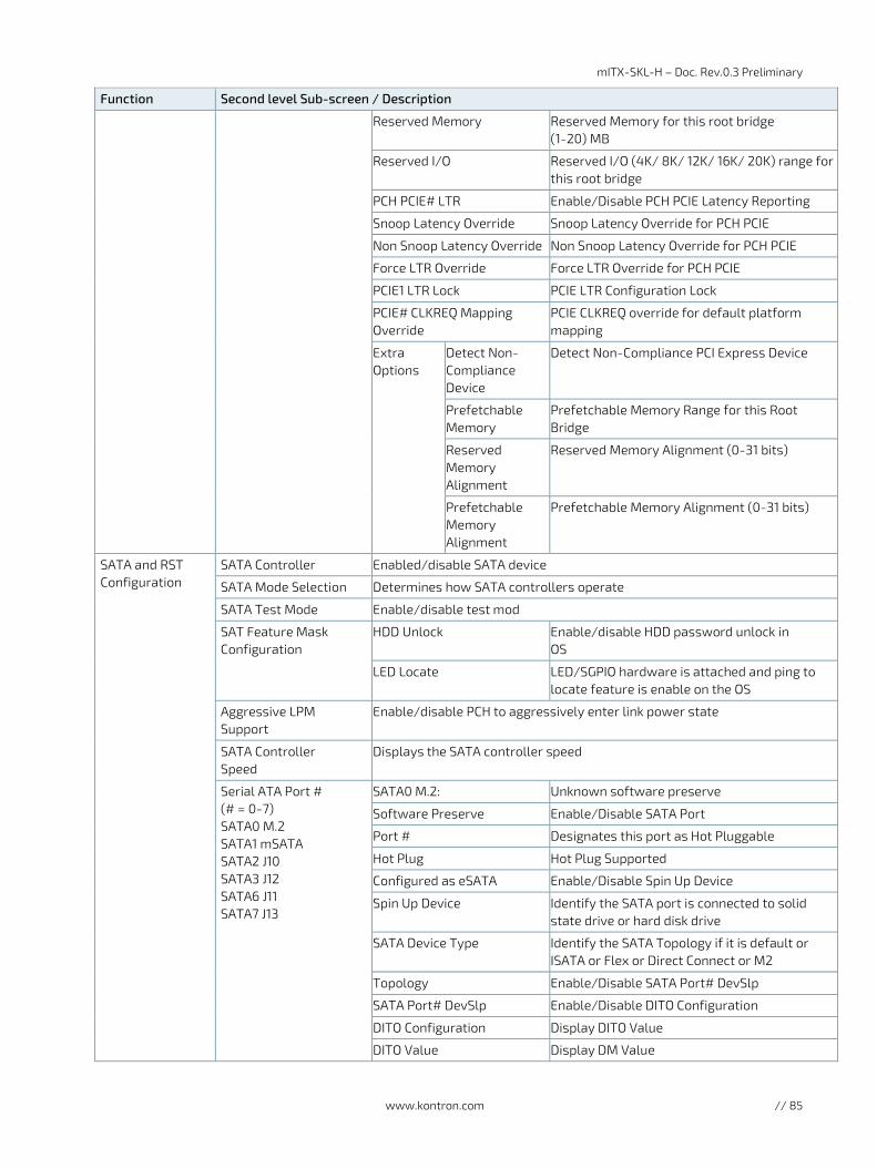
mITX-SKL-H – Doc. Rev.0.3 Preliminary
www.kontron.com // 85
Function Second level Sub-screen / Description
Reserved Memory Reserved Memory for this root bridge (1-20) MB
Reserved I/O Reserved I/O (4K/ 8K/ 12K/ 16K/ 20K) range for this root bridge
PCH PCIE# LTR Enable/Disable PCH PCIE Latency Reporting
Snoop Latency Override Snoop Latency Override for PCH PCIE
Non Snoop Latency Override Non Snoop Latency Override for PCH PCIE
Force LTR Override Force LTR Override for PCH PCIE
PCIE1 LTR Lock PCIE LTR Configuration Lock
PCIE# CLKREQ Mapping Override
PCIE CLKREQ override for default platform mapping
Extra Options
Detect Non-Compliance Device
Detect Non-Compliance PCI Express Device
Prefetchable Memory
Prefetchable Memory Range for this Root Bridge
Reserved Memory Alignment
Reserved Memory Alignment (0-31 bits)
Prefetchable Memory Alignment
Prefetchable Memory Alignment (0-31 bits)
SATA and RST Configuration
SATA Controller Enabled/disable SATA device
SATA Mode Selection Determines how SATA controllers operate
SATA Test Mode Enable/disable test mod
SAT Feature Mask Configuration
HDD Unlock Enable/disable HDD password unlock in OS
LED Locate LED/SGPIO hardware is attached and ping to locate feature is enable on the OS
Aggressive LPM Support
Enable/disable PCH to aggressively enter link power state
SATA Controller Speed
Displays the SATA controller speed
Serial ATA Port # (# = 0-7) SATA0 M.2 SATA1 mSATA SATA2 J10 SATA3 J12 SATA6 J11 SATA7 J13
SATA0 M.2: Unknown software preserve
Software Preserve Enable/Disable SATA Port
Port # Designates this port as Hot Pluggable
Hot Plug Hot Plug Supported
Configured as eSATA Enable/Disable Spin Up Device
Spin Up Device Identify the SATA port is connected to solid state drive or hard disk drive
SATA Device Type Identify the SATA Topology if it is default or ISATA or Flex or Direct Connect or M2
Topology Enable/Disable SATA Port# DevSlp
SATA Port# DevSlp Enable/Disable DITO Configuration
DITO Configuration Display DITO Value
DITO Value Display DM Value

mITX-SKL-H – Doc. Rev.0.3 Preliminary
www.kontron.com // 86
Function Second level Sub-screen / Description
USB Configuration
XHCI Disable Compliance Mode
Option to disable compliance mode True -disables compliance mode. (Default is false)
xDCI Support Enable/disable xDCI (USB OTG device)
USB Port Disable Override
Enable/disable corresponding USB port from reporting a device connection to the controller
Security Configuration
RTC Lock Enable/disable RTC lock Enable- locks bytes 38h-3Fh in lower/upper 128 byte RTC RAM bank
BIOS Lock Enable/disable PCH BIOS lock enable (BLE bit) feature
HD Audio Configuration
HD Audio Control detection of the HD-Audio device Disable- HDA unconditionally disabled Enable – HDA unconditionally enabled Auto – HD enabled if present
Audio DSP Enable/disable audio DSP
Audio DSP Compliance Mode
Specifies DSP enabled system compliance 1/ Non-UAA (IntelSST driver support only -CC_0400100) 2/.UAA (HD Audio Inbox or IntelSST driver support-CC_040380)
HDA-Link Codec Select Selects which of the following is used: Platform onboard codec (single verb table installed) or External codec kit (multiple verb table installed )
iDisplay Audio Disconnect
Disconnects SDI2 signal to hide/disable iDisplay audio codec
PME Enable Enable/disable power management wake of audio controller during POST
HD Audio Advanced Configuration
I/O Buffer Ownership Selects the ownership of the I/O buffer between Intel HD audio link and I2S port (for bilingual codecs)
I/O Buffer Voltage Select
Selects the voltage operation mode of the I/O buffer
HD Audio Link Frequency
Selects HD audio link frequency (Applicable only if HDA codec supports selected frequency)
iDisplay Link Frequency
Selects iDisplay Link frequency (Applicable only if iDisp codec supports selected frequency)
HD Audio DSP Features Configuration
Read Only field (DMIC, Bluetooth and I2S)
WoV (Wake on Voice) Enable/disable DSP feature Bitmap structure: Bit 0 – WOV Bit 1 - BT Sideband Bit 2 - Codec based VAD Bit 5 - BT Intel HFP Bit 6 - BT Intel A2DP
Bluetooth Sideband
BT Intel HFP ( read only field)
BT Intel A2DP (read only field)
Codec Based VAD
DSP Based Speech Pre-processing Disabled
Voice Activity Detection
Waves Enable/disable 3rd party processing module support (identified by GUID) Note: WOV must first be enabled as a feature to select relevant WoV IP.
DTS
IntelSST Speech
Dolby
Waves Pre-process
Audyssey
Maximum Smart AMP

mITX-SKL-H – Doc. Rev.0.3 Preliminary
www.kontron.com // 87
Function Second level Sub-screen / Description
Fortemedia SAMSoft Enable/disable 3rd party processing module support (identified by GUID) Note: WOV must be enabled first as a feature, to select relevant WoV IP.
Intel WoV
Sound Research IP
Conexant Pre-Process
Conexant Smart Amp
Realtek Post-Process
Realtek Smart Amp
Icepower IP MFX sub module
Icepower IP EFX sub module
Icepower IP SFX sub module
Custom Module ‘Alpha’
Custom Module ‘Beta’
Custom Module ‘Gamma’
Serial IO Configuration
I2C0 Controller1 Enables/disables Serial IO controller Following devices depend on each other: I2C0 and I2C1;2;3 UART0 and UART1, SPIO, SPI1 UART2 and I2C4, I2C5
I2C1 Controller2
I2C2 Controller3
SPI0 Controller
SPI1 Controller
SPI2 Controller
UART0 Controller
UART1 Controller
UART2 Controller
GPIO Controller Enable /disable the GPIO controller
Serial IO I2C0 Settings I2C IO Voltage Select Select 1.8 V or 3.3 V for the controller
Connected Device Indicate what type of device is connected to this serial IO controller
Serial IO I2C1 Settings I2C IO Voltage Select Select 1.8 V or 3.3 V for the controller
Connected Device Indicate what type of device is connected to this serial IO controller
Serial IO SPI0 Settings ChipSelect Polarity Sets initial polarity for ChipSelect signal
Serial IO UART0 Settings Bluetooth Device Enable/disable the vendor Sensor
Wireless Charging Mode Set the wireless charging mode
Hardware Flow Control When enabled configures additional 2 GPIO pads for use as RTS/CTS signals for UART
Serial IO GPIO Settings GPIO IRQ Route Route all GPIO to one of the IRQ
WITT/MITT Test Device Choose if WITT Device is used and with which controller
UART Test Device Choose if UART Test Device is used and with which controller
Additional Serial IO Device
When enabled, ACPI will report additional devices connected to Serial IO
Serial IO Timing Parameters
Serial IO timing parameters
Serial IO timing parameter ( test only)
UCSI/UCMC Device
When enabled, ACPI will report UCSI/UCMC device
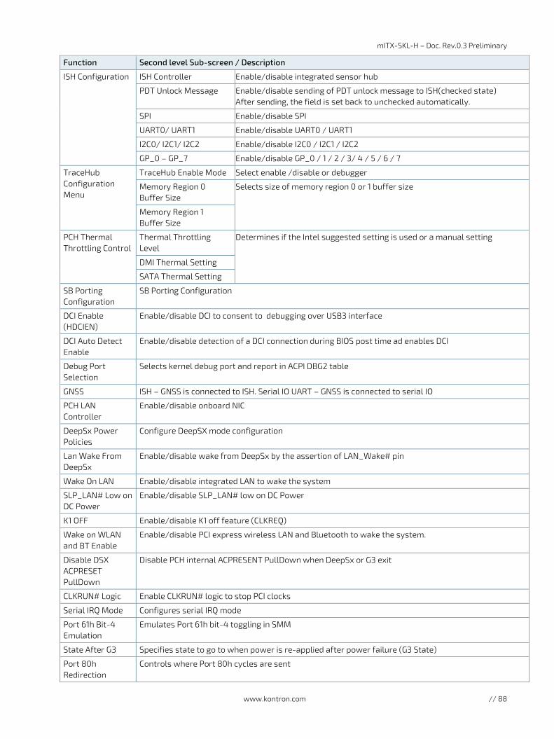
mITX-SKL-H – Doc. Rev.0.3 Preliminary
www.kontron.com // 88
Function Second level Sub-screen / Description
ISH Configuration ISH Controller Enable/disable integrated sensor hub
PDT Unlock Message Enable/disable sending of PDT unlock message to ISH(checked state) After sending, the field is set back to unchecked automatically.
SPI Enable/disable SPI
UART0/ UART1 Enable/disable UART0 / UART1
I2C0/ I2C1/ I2C2 Enable/disable I2C0 / I2C1 / I2C2
GP_0 – GP_7 Enable/disable GP_0 / 1 / 2 / 3/ 4 / 5 / 6 / 7
TraceHub Configuration Menu
TraceHub Enable Mode Select enable /disable or debugger
Memory Region 0 Buffer Size
Selects size of memory region 0 or 1 buffer size
Memory Region 1 Buffer Size
PCH Thermal Throttling Control
Thermal Throttling Level
Determines if the Intel suggested setting is used or a manual setting
DMI Thermal Setting
SATA Thermal Setting
SB Porting Configuration
SB Porting Configuration
DCI Enable (HDCIEN)
Enable/disable DCI to consent to debugging over USB3 interface
DCI Auto Detect Enable
Enable/disable detection of a DCI connection during BIOS post time ad enables DCI
Debug Port Selection
Selects kernel debug port and report in ACPI DBG2 table
GNSS ISH – GNSS is connected to ISH. Serial IO UART – GNSS is connected to serial IO
PCH LAN Controller
Enable/disable onboard NIC
DeepSx Power Policies
Configure DeepSX mode configuration
Lan Wake From DeepSx
Enable/disable wake from DeepSx by the assertion of LAN_Wake# pin
Wake On LAN Enable/disable integrated LAN to wake the system
SLP_LAN# Low on DC Power
Enable/disable SLP_LAN# low on DC Power
K1 OFF Enable/disable K1 off feature (CLKREQ)
Wake on WLAN and BT Enable
Enable/disable PCI express wireless LAN and Bluetooth to wake the system.
Disable DSX ACPRESET PullDown
Disable PCH internal ACPRESENT PullDown when DeepSx or G3 exit
CLKRUN# Logic Enable CLKRUN# logic to stop PCI clocks
Serial IRQ Mode Configures serial IRQ mode
Port 61h Bit-4 Emulation
Emulates Port 61h bit-4 toggling in SMM
State After G3 Specifies state to go to when power is re-applied after power failure (G3 State)
Port 80h Redirection
Controls where Port 80h cycles are sent

mITX-SKL-H – Doc. Rev.0.3 Preliminary
www.kontron.com // 89
Function Second level Sub-screen / Description
Enhanced Port 80 h LPC Decoding
Supports word/dword decoding of port 80h behind LPC
Compatibility Revision ID
Enable/disable PCH compatibility Revision ID feature
PCH Cross Throttling
Enable/disable PCH cross throttling feature Note: Only ULT supports this feature.
Disable Energy Reporting
Enables/disables PCH energy reporting feature Note: SET to disabled. This feature is only for test purposes.
Enable TCO Timer Enable/disable TCO timer If disabled, PCH ACPI timer is disabled and stops TCO timer.
PCIe PLL SSC Selects the PCIe PLL SSC percentage (Range: 0.0 % - 2.0 %) Auto keeps hardware default, no BIOS override.
Unlock PCH P2SB Unlock PCH P2SB SBI and configuration space by PSF
PMC Read Disable Enable/disable this test feature for PMC XRAM read
Flash Protection Range Registers (FPRR)
Enable/disable Flash protection range registers
SPD Write Disable Enable/disable the setting for SPD write disable. For security, recommendations SPD write disable bit must be set.
ChipsetInit HECI Message
Enable/disable ChipsetInit HECI message
Bypass ChipsetInit Sync Reset
Sets this option to skip ChipsetInit sync reset

mITX-SKL-H – Doc. Rev.0.3 Preliminary
www.kontron.com // 90
9.2.4. Security Setup Menu The Security Setup menu provides information about the passwords and functions for specifying the security settings. The passwords are case-sensitive. The mITX-SKL-H provides no factory-set passwords.
If there is already a password installed, the system asks for this first. To clear a password,
simply enter nothing and acknowledge by pressing <RETURN>. To set a password, enter it twice and acknowledge by pressing <RETURN>.
Table 45: Security Setup Menu Functions
Function Description
Administrator Password Sets administrator password
User Password Sets user password
Secure Boot Attempt Secure Boot Secure Boot activated when platform key (PK) is enrolled, System mode is user deployed, and CSM function is disabled.
Secure Boot Mode Selects between standard and custom. Customer mode – secure Boot variables can be configured without authentication.
Key Management Enables expert users to modify secure Boot Policy variables without full authentication.
If only the administrator’s password is set, then only access to setup is limited. The password is only entered when entering setup.
If only the user’s password is set, then the password is a power on password and must be entered to boot or enter setup. Within the setup menu the user has administrator rights.
Password length requirements are maximum 20 characters and minimum 3 characters.
9.2.4.1. Remember the password It is highly recommended to keep a record of all passwords in a safe place. Forgotten passwords results in being locked out of the system.
If the system cannot be booted because the User Password or the Supervisor Password are not known, see Chapter 9.6 Firmware Update for information about clearing the uEFI BIOS settings, or contact Kontron Support for further assistance.
HDD security passwords cannot be cleared using the above method.

mITX-SKL-H – Doc. Rev.0.3 Preliminary
www.kontron.com // 91
9.2.5. Boot Setup Menu The Boot Setup menu lists the for boot device priority order, that is generated dynamically.
Table 46: Boot Setup Menu Functions
Function Description
Setup Prompt Timeout Displays number of seconds that the firmware waits before initiating the original default boot selection. 65535(OxFFFF) means indefinite waiting.
Bootup NumLock State Selects keyboard NumLock state
Quiet Boot Enable/disable Quiet Boot option
Boot Option #1 Sets the system boot order
Fast Boot Enable/disable boot with initialization of a minimal set of devices required to launch active boot option. This has no effect for BBS boot options.
New Boot Option Policy Controls placement of newly detected UEFI boot options
9.2.6. Save & Exit Setup Menu The Exit Setup menu provides functions for handling changes made to the UEFI BIOS settings and the exiting of the Setup program.
Table 47: Save and Exit Setup Menu Functions
Function Description
Save Changes and Exit Exits system after saving changes
Discard Changes and Exit Exits system setup without saving changes
Save Changes and Reset Resets system after saving changes
Discard Changes and Reset Resets system setup without saving changes
Save Changes Saves changes made so far for any setup option
Discard Changes Discards changes made so far for any setup option
Restore Defaults Restores/loads default values for all setup options
Save as User Defaults Saves changes made so far as user defaults
Restore User Defaults Restores user defaults to all setup options
UEFI Built-in EFI shell Attempts to launch the built-in EFI Shell
Launch EFI Shell from File System Device Attempts to launch EFI Shell application (Shell.efi) from one of the available file system devices

mITX-SKL-H – Doc. Rev.0.3 Preliminary
www.kontron.com // 92
9.3. The UEFI Shell
The Kontron UEFI BIOS features a built-in and enhanced version of the UEFI Shell. For a detailed description of the available standard shell scripting, refer to the EFI Shell’s User Guide. For a detailed description of the available standard shell commands, refer to the EFI Shell Command Manual. Both documents can be downloaded from the EFI and Framework Open Source Community homepage (http:/ /sourceforge.net/projects/efi-shell/files/documents/).
Please note that not all shell commands described in the EFI Shell Command Manual are provided by the Kontron UEFI BIOS.
9.3.1. Introduction, Basic Operation The UEFI Shell forms an entry into the UEFI boot order and is the first boot option by default.
9.3.1.1. Entering the UEFI Shell To enter the UEFI Shell, follow the steps below:
1. Power on the board.
2. Press the ESC key within 5 seconds after a message such as the one below appears:
UEFI shell only support FAT partition (Exclude FAT64/exFAT)
If the disk drive is FAT partitioned, BIOS will display
fsn:
If the disk drive is not FAT partitioned, shell will display
blk#
(where # is 0, 1 or 2 depending on the number of disks connected.
The output produced by the device mapping table can vary depending on the board’s configuration.
If the ESC key is pressed before the 5-second timeout has elapsed, the shell prompt is shown:
Shell>
9.3.1.2. Exiting the UEFI Shell To exit the UEFI Shell, follow one of the steps below:
1. Invoke the exit UEFI Shell command to select the boot device in the boot menu for the OS to boot from.
2. Reset the board using the reset UEFI Shell command.

mITX-SKL-H – Doc. Rev.0.3 Preliminary
www.kontron.com // 93
9.4. UEFI Shell Scripting
9.4.1. Startup Scripting If the ESC key is not pressed and timeout has run out, the UEFI Shell tries to execute the startup scripts automatically. It searches for scripts and executes them in the following order:
1. Kontron flash-stored startup script
2. The UEFI specified startup script is startup.nsh. This script must be located on the root of any of the attached FAT formatted disk drives.
3. If the startup scripts is not present or the startup script terminates, the default boot order is continued.
The default start up script is startup.nsh.
Startup,nsh can call Kontron’s special Kontron flash-stored startup script if present.
9.4.2. Create a Startup Script Startup scripts can be created using the UEFI Shell built-in editor edit or under any OS with a plain text editor of your choice. To create a startup shell script, simply save the script on the root of any FAT-formatted drive attached to the system.
9.4.3. Examples of Startup Scripts
9.4.3.1. Execute Shell Script on Other Harddrive This example (startup.nsh) executes the shell script named bootme.nsh located in the root of the first detected disc drive (fs0).
The startup.nsh content:
fs0:
bootme.nsh
9.4.3.2. Boots Windows 8.x from Shell Script This example assumes the use of a Microsoft Win 8.x disc and fs0: point to its FAT32 partition. Windows 8.x boots from the shell script. Similar examples can apply to Linux OS.
Bootme.nsh content:
\EFI\Boot\bootx64.efi

mITX-SKL-H – Doc. Rev.0.3 Preliminary
www.kontron.com // 94
9.5. Firmware Update
Firmware updates are typically delivered as a ZIP archive containing the BIOS Flash ( fpt.efi or fpt64.efi ) Tool and the firmware images. The content of the archive with the directory structure must be copied on a data storage device with FAT partition. The user can run the “Upd.nsh” from the folder to update the firmware or to manually update the BIOS image from a particular folder. The tools is running under the UEFI shell.
9.5.1. Updating Procedure BIOS can be updated with the Intel fpt.efi by following the procedure below:
1. Before flashing, unlock “BIOS Lock” disable this feature in the BIOS menu. o BIOS Menu>Chipset> PCH-IO Configuration> Security Configuration> BIOS lock> Disable
2. Copy following files to a USB stick (fpt.efi, fparts.txt, bios_image.bin) 3. Boot to EFI shell and enter the following command:
o fpt.efi-f bios_imge.bin -savemac 4. Wait until flashing is successful and then power cycling the board.
Do not press “CTRL + Alt + Del” to reboot board.
CTRL + Alt + Del will not clear the lock bit (including security related lock bit ), because it is a warm reset.

mITX-SKL-H – Doc. Rev.0.3 Preliminary
www.kontron.com // 95
List of Acronyms
The following table does not contain the complete acronyms used in signal names, signal type definitions or similar. A description of the signal is included in the relevant connector section within this User Guide. See Chapters 6 and 7.
ACPI Advanced Configuration and Power Interface (standard that operating systems use to perform discovery and configuration of computer hardware components, to perform power management...)
ADC Analog Digital Converter
AHCI Advanced Host Controller Interface
AMT Active Management Technology (intel)
API Application programming interface, a set of routine definitions, protocols, and tools for building software and applications
AT Adcanced Technology // Anti-Theft Technology
ATA AT Attachment, interface standard for the connection of storage devices
ATX Advanced Technology Extended (motherboard configuration specification)
ADC Analog Digital Converter
BIOS Basic Input/Output System (type of firmware used to perform hardware initialization during the booting process)
BSP Board support package ( implementation of specific support code (software) for a given (device motherboard) board that conforms to a given operating system)
BTX Balanced Technology Extended (motherboard configuration specification)
CMOS Complementary Metal Oxide Semiconductor (technology for constructing integrated circuits)
COM Communication Equipment (Serial Bus)
CPU Central Processing Unit
DAC Digital Analog Converter
DDC Display Data Channel
DDR3 Double Data Rate (SDRAM interface)
DirectX Collection of application programming interfaces (APIs) for handling tasks
DP Display Port
DXVA DirectX Video Acceleration
ECC Error Checking and Correction
eDP Embedded Display Port, standardized display panel interface for internal connections
EFI Extensible Firmware Interface
EHCI Enhanced Host Controller Interface
EMI Electromagnetic Interference
ESD Electrostatic discharge
GBE Gigabyte Ethernet
GND Ground (Earthing)
GPIO General-purpose input/output
HBR2 High Bit Rate (Video format)
HD High Definition Audio (Intel)
HDD Harddisk Drive
HDMI High-Definition Multimedia Interface
LAN Local Area Network
LPC Low Pin Count (Serial Bus)
LVDS Low-voltage differential signaling
MDI Media Dependent Interface
mITX MiniITX (form factor for motherboards)
mPCI Mini PCI (small form factor expansion card utilizing serial PCI Express and USB interfaces)
mPCIe Mini PCI Express (a small form factor expansion card utilizing serial PCI Express and USB interfaces)
mSATA Mini SATA (interface to Harddisk oder Solid State Disks)
MTBF Mean Time Between Failures
NCQ Native Command Queuing
OpenGL Application programming interface (API) for rendering vector graphics
PCB Printed Circuit Board
PCI Peripheral Component Interconnect (local computer bus for attaching hardware devices)
PEG PCI Express for Graphics
PCH Platform Controller Hub
PS/2 Interface for connecting keyboards and mice
PSU Power Supply Unit

mITX-SKL-H – Doc. Rev.0.3 Preliminary
www.kontron.com // 96
PWM Pulse-width modulation
PXE Preboot eXecution Environment, standardized client-server environment that boots a software assembly
RAID Redundant Array of Independent Disks
RBR Reduced Bit Rate (Video format)
RoHS Restriction of Hazardous Substances
RRT Rapid Recover Technology (Intel)
RST Rapid Storage Technology (Intel)
SATA Serial ATA (bus interface)
SIM SIM card, subscriber identification module
SMB System Management Bus, single-ended simple two-wire bus for the purpose of lightweight communication
SNR Signal-to-Noise Ratio
SPD Serial Presence Detect
SPDIF Sony/Philips Digital Interface Format, type of digital audio interconnect
SPI Serial Peripheral Interface
TDG Thermal Design Guideline
TPM Trusted Platform Module, standard for a secure cryptoprocessor
TRIM Command in the ATA command set
TXT Trusted Execution Technology (Intel)
UDIMM Unregistered Dual In-line Memory Module
UEFI Unified Extensible Firmware Interface
USB Universal Serial Bus
VC1 Video Coding format
VGA Video Graphics Array, video format
vPRO Set of features built into a PC's motherboard and other hardware (Intel)
VT-d Virtualisation Technology for Directed I/O (Intel)
WES7 Windows Embedded System 7
XHCI Extensible Host controller Interface

mITX-SKL-H – Doc. Rev.0.3 Preliminary
www.kontron.com // 97
CORPORATE OFFICES
EUROPE, MIDDLE EAST & AFRICA
NORTH AMERICA ASIA PACIFIC
Lise-Meitner-Str. 3-5 86156 Augsburg Germany Tel.: + 49 821 4086-0 Fax: + 49 821 4086-111 [email protected]
14118 Stowe Drive Poway, CA 92064-7147 USA Tel.: + 1 888 294 4558 Fax: + 1 858 677 0898 [email protected]
1~2F, 10 Building, No. 8 Liangshuihe 2nd Street, Economical & Technological Development Zone, Beijing, 100176, P.R. China Tel.: + 86 10 63751188 Fax: + 86 10 83682438 [email protected]


