46
Mälardalen University

Mälardalen University

05-02-21
Addre ss Vis it in g addre ss Phone Fax Intern et Box 337 Polacksbacken +46 18 471 6847 +46 18 511925 [email protected] SE-751 05 Uppsala, Sweden http://www.artes.uu.se/
Preface This volume contains the papers presented at the 5th ARTES Graduate Student Conference, held at Mälardalen University, from February 22-23, 2005. As of today, 100 graduate students are active the ARTES network by registering as Real-Time Graduate Students. They thereby get access to the benefits provided by ARTES. This includes participation at the ARTES Summer School and ARTES funded PhD courses, mobility support provided by ARTES to new PhD students and public relation activities by ARTES industry ambassador to bring the research results to the public and industry. The present 100 real-time graduate students as well as the about 60 ARTES Real-Time doctors clearly indicate that a substantial amount of real-time research is conducted in Sweden. Due to ARTES and other efforts, it is fair to say that Sweden is one of the world-leaders in real-time systems research. We have an exiting meeting ahead of us. The main idea with the ARTES Graduate Student Conference is to provide a forum for technical presentations and discussions among the Swedish graduate students active in the real-time area. For newly recruited graduate students it will provide an opportunity to experience “a real conference situation” (maybe) for the first time. For everyone, the conference will be an excellent opportunity to, in a relatively short time, get an overview of the current state of the national research. This year we have included a visit to ABB Robotics in co-operation with SAVE-IT. ARTES programme director from the start until 2004-12-31 will present the research at Mälardalen Real-Time Center and as a bonus the conference has been planned to end in conjunction with the start of the guest lectures by Wolfgang Weck and Mikael Åkerholm in the ARTES course Advanced Component Based Software Engineering. The papers included in this volume indicate width and quality of Swedish Real-Time research. We are certain that the conference will be an event with intense technical and other discussion. Enjoy it! Paul Pettersson and Roland Grönroos for the ARTES Programme http://www.artes.uu.se/

PhD Student Kick-Off 2005in Västerås
February 22-23
ScheduleTuesday February 22
11.30 Lunch at Rosenhill, thereafter departure to ABB13.00 ABB Robotics in collaboration with SAVE-IT16.00 Session 1 in room R1-142. chair: Roland
Paul Pettersson, A few words about ARTESJohan Erikson, The Parallel PLEX ProjectJianlin Shi, Model Based Development andCompetence Integration within Mechatronics
17.00 BreakSession 2 in room R1-142. chair:
Erik Kuiper, Robust Real-time Communication inDynamic Wireless Ad Hoc NetworksViacheslav Izosimov, Design Optimization ofTime- and Cost-Constrained Fault-TolerantDistributed Embedded SystemsChrister Gerdtman, Alternative input devices
19.30 Dinner at STRIKE, Torggatan 1
Wednesday February 23Room: R1-142
9.00 Hans Hansson et. al. MRTC activities10.00 Break with coffe10.15 Session 3 chair:
Najeem Lawal, Global Block RAM Allocation andAccesses for FPGA Implementation of Real-TimeVideo Processing SystemsNiklas Lepistö, FPGA based Surveillance andControl Computer for Customer SpecificApplicationsFredrik Törner, Design of Electrical Architecturesfor Safety Cases
11.00 Session 4 chair:Johan Andersson, to be announcedPavel Krcal, REMODEL in TimesJohn Håkansson, UML SPT in Times
12.00-13.00 Lunch13.15 - 17.00 Possibility to attend the guest lectures in

the ADVANCED COMPONENT-BASED SOFTWAREENGINEERING course.
Wolfgang Weck - Eclipse Integration FrameworkMikael Åkerholm - SaveCCM Component model
Updated: 21-Feb-2005 11:15 E-mail: [email protected] Web: www.artes.uu.se Location: http://www.artes.uu.se/events/gsconf05/schedule.shtml

Skultunavägen
Järnbruksgatan
Sjöhag
sväg
en
Saltängsvägen
Lisjögatan
Surahammarsv.
Skälby-motet
Bäckby-motet
Narvavägen
Råbyleden
VallbyledenSkerikesvägen
Vallby-motet
Vallbyleden
Drottninggatan
Stora Gatan
Önstavägen
Gry
tavä
gen
Norrleden
Vasagatan
Rocklunda-motet
Skallbergs-motet
Berg
slags
väge
n
Emaus-motet
Korsängs-motet
Kopp
arbe
rgsv
.
N. Ringv.
Södra Ringvä
gen
Björnövägen Väderleksg.
Häs
slög
atan
Hälla-motet
Stockholmsv.
Tortu
navä
gen
Öst
erle
den
Talltorps-motet
Malmab
ergsg
. Tråddragargatan Bjurhovdag.
Tillbergaleden
Nyängsleden
ill Fagersta, Surahammar
Rönnbyvägen
Till Skultuna
Alve
stav.
Till
Sa
Till Irsta
Till Stockh
olm
Till Tortuna
Till Ir
Till
Tillb
erga
Till Dingtuna
Köpingsvägen
Folkparks-motet
Kungsä
ngsg
.
ll Oslo
, Köping
Johannisbergsv
Anemonvägen
Nordanby-motet
Lunda-motet
Lundaleden
Lugn
a G
atan
Badelundavägen
Nor
rlede
n
Tortuna-motet
Bjurhovda-motet
Finnslätts-motet
Malmabergsmotet
Erikslunds-motet
Hammarby-rampen
ÖSTERMÄLARSTRAND
VIKSÄNG
ÄNGS-GÄRDET
HEMDAL
KLOCKAR-TORP
S. SKILJEBO
SKILJEBO
N. SKILJEBO
TALLTORP
HAMREFRAMNÄS
HÄSSLÖ
HÄLLA
BERGHAMRA
BJURHOVDA
BRANDTHOVDA
MALMABERG
HAGA
N. HAGA
FINN-SLÄTTEN
NORDANBYGÄRDE
GIDEONS-BERG
NORDANBY
ROCKLUNDA SKALL-BERGET
TUNBY
VEGA
KRISTIANS-BORG
KARLS-DAL
AROS-LUND
STENBY
TUNBYTORP
N. TUNBYTORP
HÖKÅSEN
ÖNSTA N. GRYTA
S. GRYTA
ÅS-HAGEN
RÖNNBY
BILLSTA
BROTTBERGA
VALLBY
ERIKSLUND
PETTERS-BERG
VETTERS-LUND
JAKOBSBERG
STALL-HAGEN
STOHAGEN
VETTERS-TORP
HAMMARBY
RÅBY
SJÖHAGEN
SALTÄNGEN
HACKSTA
BÄCKBY
SKÄLBY
MUNKBOÄNGEN
ERIKSLUNDSIND. OMR CENTRUM
LUNDA
V. SKÄLBY
HAGABERG
Ö. SKILJEBO
KOPPAR-LUNDEN
HAMMARBYSTADSHAGE
BLÅSBO
MUNKÄNGEN
FÅGELVIK
Svartån
MÄLAREN
67
66
E18
E18
Så här hittar du till/The Quickest Route to
Roboticsi Västerås/in Västerås
Central-station
Västeråsflygplats

Finnslätten
347
358 357 391
351
326
346
342
340
330
331
332336
343
350
396
337
Term
inal
väge
n
Wijkmansgatan
NorrledenÖsterleden
Lugn
a ga
tan
344
Reception
Busshållplats/Bus Stop
Mot CentrumMotSalavägen
Bet
ongg
atan
Wijkmansgatan
Effe
ktga
tan
393
LundaledenMot Salavägen
Ele
ktro
nikg
atan
Qui
ntus
väge
nR
obot
väg.
Hydrovägen
Ban
mat
arvä
gen
Turb
oväg
en
Hä
rvst
ige
n
Tekn
ikvä
gen
Tvärleden Tvärleden Nätverksgatan
Robotvägen
Kab
elgr
änd
341
Lugn
a ga
tan
Kre
tsko
rtsv
ägen
ManufacturingIndustries
Robotics
Elmotorgatan
359
ABBUniversity
ABB Hälsan
Hyd
rovä
gen
Svartån
Stora Gatan
Vasagatan Kopparbergsvägen
Södra Ringvägen
Ham
n gatan
Västra Ringvägen
Östra Ringvägen
Pilgatan
Kungsängsg
atan
Björnövägen
Mal
mab
ergs
gata
n
Enge
lbre
ktsg
atan
Biskopsgatan
Karlsg.
Stora Gatan
Östermalmsgatan
Timmermansg.
Munkgatan
Hant- verkarg.
Snickarg.Smedje-
Domkyrkoespl.Nygat
an
Västra Utanbyg.
Knutsgatan
Her
rgär
dsg.
arlsgatan
Braheg.
Valling.
Skolgatan
Kyrkbacksg.
Blåsbog.
Gåsm
yreg.
sgatan
V. Kyrkog.
Ö Kyrkog.
N. Källgatan.
Slottsg.Bondeg.
Kungsg.
Köpmang.
Västgöteg.
Skepparb.
Hållgatan
Sigurdsg.
nagatan
Tess
ing.
Linn
ég.
StoraTorget
Fiskar-torget
Asea-torget
Floragatan
Mim
ergatan
Utanby-
Rudbecksg.
Allég.
Källgatan
sgat
an
sins
väge
n
Ängs-
gärdsg.
Pilgatan
Gasverksg.
Trefasgatan
Kass-
örsg.
Lidmansv.
msg.
Bonde
-ba
cken
Övre
Kungsg.
agsg
atan
Gustavsg.
gsg.
at
Claréusg.
Trappgr.
Lant-
mäterib.
Sko-
makarg.
Badhusg.
Storbron
Torgg.Apotekar-bron
Lykt-
tändargr.
Vattu
g.
Djä
kneg
.
Rektorsg. Lilla
Nyg.
Karlsgatan
tra K
ajen
Lillå
kaje
n
Sturegatan
Öde-
marks-
stigen
V. Skepparb.
Slotts-stige
Sigurdsgata
n
Sjö-tull
-ans-
backen
K
gatan
gatan
Skvaller-
gränd
ringsgatan
arlundsvägen
Glödgargr.
Glö
dgar
gr.
Lins
laga
rgr.
Sintervägen
Skivfilargr.Stansargr.
Alléstigen
Metallverksgatan
s verksg.
Domkyrka
Stadshus
Slott
Bibliotek
Central-stationPolis
Teater
ArosCongress
Center
Buss-terminal
Läns-museum
Högskola
Forum
P
P
P
P
P
PP
P
P
PP
P
FinnslättenABB Automation Technology Products ABRobotics har kontor /verkstad i byggnaderna331, 330, 332, 346, 326, 342Robotics has offices and workshops in buildings 331, 330, 332, 346, 326, 342
Robotics University building 357
ABB Automation Technology Products ABRoboticsHydrovägen 10721 68 Västeråstel 021-34 40 00
ReceptionReceptionBusshållplatsBus stopBuss till och från Arlanda: Bussterminalen vid järnvägsstationArlanda - Västerås bus route: Bus terminal at the railway station and Scandic Hotel
Buss från centrum till Finnslätten: Linje 11 från Stora GatanCity centre - FinnslättenBus route: Use bus no. 11 from Stora Gatan
Aros Congress Center (ACC)Konserhuset/Concert hall
Polisstation/Police station
ABB’s huvudkontor/ABB head office
Radisson SAS HotelStadshotelletComfort Hotel Etage Scandic HotelCentralstation/Railway station
Västerås Flygplats/Västerås Airport
Turistbyrån/Tourist information
Apoteket/Pharmacy
Postkontor/Post office
ForexStadsbiblioteket/Library15
14
13
12
11
10
9
8
7
6
5
4
3
2
1
15
14
13
12
8
7
6
54
3
21
9
11
10

Position Statement - The Parallel PLEX Project
Johan EriksonDepartment of Computer Science and Electronics
Malardalen [email protected]
http://www.idt.mdh.se/personal/jen02
1 Background
The Parallel PLEX Project is a co-operation between Ericsson AB and the Department of Com-puter Science and Electronics at Malardalen University. The project is facing the followinggeneral situation:
A complex legacy software system with independent jobs/tasks that executes in a non-preemptive, priority-based fashion. Since parallel processing was not an issue at the time thesystem was designed, programmers have assumed sequential execution and exclusive accessto data, both in the design phase and (possibly years) later when the implementation has beenupdated.
The problem arises when the current single-processor architecture is to be replaced by amulti-processor ditto - How is the system to be parallelized? By simply moving the softwarefrom the old architecture to the new, it is most likely that the programs will break sinceindependent, and concurrently executing, jobs may access and update the same data.
2 The AXE System
Our ”instance” of the general problem described in Section 1 is the AXE telephone exchangesystem, Fig 1, in general, and the language PLEX, which is used to program the functionalityin central parts of the AXE system, in particular. (PLEX is covered in Section 3.)
CPS
AXE
APZ APT
. . .. . . . . . . . .. . .
Figure 1: Structure of the AXE telephone exchange system. PLEX is used to program theCentral Processor Sub-system, CPS.
The AXE system, developed in its earliest version in the beginning of the 1970s, is struc-tured in a modular and hierarchical way. It consists of the two main parts:
APT: The telephony or switching part
1

APZ: The control part including central and regional processors
which both consist of hardware and software. The two main parts are divided into subsys-tems, where the part that is of interest for us is the Central Processor Subsystem (CPS), seeFig. 1.
In the current architecture, the control system (APZ) consists of a Central Processor (CP)(which in turn consists of a single CPU and additional software) and a number of RegionalProcessors (RP), see Fig. 2. Call requests are received by the RP’s, inserted into job buffers,and processed by the CP. Due to the ”pseudo-parallel” structure of PLEX (described in thefollowing section), parallel processing seems like a natural choice to increase performanceand through-put in the AXE system1, but as will be discussed in Section 4, we are facingexactly the same problem with the softare as was described in Section 1.
RP
RP
CPU
CP
Figure 2: Call requests received by Regional Processors (RP) and processed by the CentralProcessor (CP).
3 PLEX, Programming Language for EXchanges
The language PLEX, is a pseudo-parallel and event-driven real-time language developed byEricsson. The language has a signal paradigm as its top execution level, and it is event-drivenin the sense that only events, encoded as signals, can trigger code execution. A typical eventis an incoming call request (see Fig. 2).
A PLEX program file (called a block) is divided in several, independent sub-programs, seeFig. 4 (a), which can be executed in any order. One or several sub-programs constitutes aJob, which is a continuous sequence of statements executed in the processor. This means thatthe execution of a PLEX program consists of the execution of a number of independent and”parallel” jobs. However, the jobs are not executed truly in parallel: rather, when spawned,they are put in one of four queues, of different priority, and sequentially executed in a non-preemptive fashion, Fig 3, thus the term ”pseudo-parallel”. Jobs communicate and controlother jobs by the usage of signals.
The entry points of the sub-programs are the only entry points to a block. Variables aredeclared in a common data area, and they have their scope inside the block they are declaredin. It is not possible to access variables from another block, except through via one of thesub-programs (in that block).
1A thorough description of the AXE system, as well as of the PLEX language (which we only cover briefly in Section3), is given in [EL02]
2

Timeblock 1 block 3block 2
enter
send
exit enter
send
send
exit enter
enter
send
exit
signal 1
signal 2
signal put injob queue
signal 5
signal put injob queue
signal put injob queue
signal 3
signal 4exit
Figure 3: The execution model of PLEX.
Due to the information hiding and data encapsulation, PLEX blocks can be thought of asobjects, and therefore PLEX may be seen as an early object-based language, see Fig. 4 (a).
ENTRY POINTPLEX Code
EXIT POINT
Code
Code
Code
Code
COMMONDATA AREA
PLEX program file (Block)
Sub-program
Sub-pgm 1
Sub-pgm 2
Sub-pgm 3
Sub-pgm 4
... ... ... Sub-pgm n
Variable ADATA AREA
(a) (b)
Figure 4: PLEX blocks: could be seen as objects (a), but also with potential conflicts (b).
4 The Problem
In the current single-processor architecture, there can be no conflicts between the independentsub-programs that access the same data area since they are executed in sequence. But, movingto a multi-processor environment, where new jobs would be forked off as parallel threadsinstead of being buffered, introduces the following problem: several, independent, jobs mayexecute code (sub-programs) from the same block, where the sub-programs access the samedata, see Fig. 4 (b).
The problem could for instance be solved by (1) extending PLEX with mechanisms to pro-tect shared variables (e.g., with a lock), rewrite and recompile the code; or (2) replace PLEX
3

with a language originally designed for parallel execution, and then rewrite the system.However, these solutions have the following drawbacks:
• First of all - The AXE system consists of 20 Mlines of PLEX code! This fact makes anyattempt to rewrite the entire system impossible due to time and money.
• It will probably be hard to find a language with a similar execution model as PLEX -which would be an absolute necessity if PLEX is to be replaced.
There have been attempts to introduce other languages, like C++, and let the systemexecute PLEX code as well as C++ code. However, these attempts have failed, mostlikely due to the different execution models.
• Even if a suitable language (to replace PLEX with) would be found, one would have todecide on the following; (1) Either the language has to be backward compatible withPLEX to prevent rewriting the entire system; or (2) existing customers would have tore-invest in a new system since their existing equipment would not be compatible withthe new.
5 Our Approach
We believe that the only practical solution is to find methods that decides when parallel ex-ecution of the current software is safe, i.e., when parallel execution of jobs yields the samebehavior as sequential execution without resulting in data interference, Fig. 4 (b).
We don’t think that the need to add synchronization primitives to some blocks (and thenre-compile them) can be totally eliminated, but our goal is to substantially reduce the numberof blocks that has to be modified in this way.
Our approach is to use program analysis to distinguish between PLEX blocks that can /can not execute in parallel, and verify the analysis with formal semantics.
• The program analysis phase will reveal how variables are read from / written to, and alsoif two jobs interfere in, or communicate through a variable. The first part (read/write)is already implemented in the PLEX compiler [AE00], whereas the second has beendiscussed by Lindell [Lin03].
These steps will allow us to decide on whether two jobs can execute in parallel or not,which will be the basis for the run-time scheduling.
• The formal semantics, which is a conventional structural operational semantics in thestyle used in [NN92], will be developed in three steps.
1. The first step is to define the semantics for sequential execution of PLEX in the cur-rent single-processor architecture, i.e., a specification/formalization of the behaviorof PLEX in the system as it is today. This step has been presented as a TechnicalReport [Eri03], as well as at a workshop on Applied Semantics [EL04].
2. The second step will specify how PLEX should behave in a chosen multi-processorparadigm without changes in the language, i.e., without synchronization primi-tives.
3. The last step will specify the semantics for ”Parallel-PLEX”, i.e., PLEX with addi-tional synchronization primitives.
4

Compile-timeAnalysis
Analysis ofvariable usage
ClassifyingSub-programs
Run-time Scheduling(Parallel Execution)
SequentialSemantics
Schedule consistent with semantics?
Parallel Semanticswithout synchronization
Parallel Semanticswith synchronization
Figure 5: The approach to solve the problem.
The semantics will then be used to verify the correctness of the decisions taken in the programanalysis phase. The approach, with the single sub-steps, are shown in Fig. 5.
Besides ensuring the correctness of parallel execution, we also aim at being able to staterules for how to (in a first step) adapt PLEX programs manually for parallel execution, and(in a second step) automate this with the program analysis.
6 A Formal Semantics for PLEX
If we look at Fig. 5, our work up til today has mainly been focused on developing the formalsemantics for PLEX, why we end this report with a brief summary of the semantics.
As stated earlier (Section 5), we have chosen a conventional structural operational seman-tics to model the behavior of PLEX, where the execution of statements is modeled by statetransitions of the form
〈S, s〉 ⇒ s′
i.e., the execution of the statement S from an initial state s results in a new state s′. Thismeans that the key thing at this point is to define the state of the system which is to be modeled,and since PLEX allows different kinds of unstructured jumps, we first introduce a virtualstatement counter, VSC, which identifies the current statement to be executed. This counteris made explicit in the program state and is used in the following way:
〈GOTO label, s〉 ⇒ s[VSC �→ ADR[[label]]]
i.e., the execution of the GOTO statement, from the initial state s, results in a new state wherethe next statement to be executed is the statement found at label.
Apart from this counter, the state is defined by the contents in the memory, including dif-ferent data areas and job queues.
When we move to a multi-processor architecture (with k processors), the state transitionswill have the form
〈S, i, s〉 ⇒ s′
where we now has made explicit where the statement is executed (on processor P i).
5

At this stage, the processors are made explicit in the system state, and with | as our paral-lelizing operator, we use the notation Pi|Pj to denote that processors Pi and Pj may executein parallel.
The above leads to following, global, state transitions
〈S, i, s〉 ⇒ s′
〈. . . | Pi | . . . , si . . . , sG〉 ⇒ 〈. . . | P ′i | . . . , s′i . . . , sG〉
to capture that there is a global change in the state
〈. . . | Pi | . . . , si . . . , sG〉 ⇒ 〈. . . | P ′i | . . . , s′i . . . , sG〉
if there is a valid, local transition of the form 〈S, i, s〉 ⇒ s′
References
[AE00] J. Axelsson and J. Erikson. SAPP, Theories and Tools for Execution Time Estimationfor Soft Real Time (Communication) Systems. Master’s thesis, Malardalen University,2000.
[EL02] J. Erikson and B. Lindell. The Execution Model of the APZ/PLEX - An InformalDescription. Technical report, Malardalen University, 2002.
[EL04] J. Erikson and B. Lisper. A formal semantics for PLEX. In Proceedings of the 2ndAPPSEM II Workshop, APPSEM’04, Tallin, 14-16 April 2004.
[Eri03] J. Erikson. A Structural Operational Semantics for PLEX. MRTC Report, ISSN 1404-3041 ISRN MDH-MRTC-166/2004-1-SE, Malardalen University, 2003.
[Lin03] B. Lindell. Analysis of reentrancy and problems of data interference in the parallelexecution of a multi processor AXE-APZ system. Master’s thesis, Malardalen Univer-sity, 2003.
[NN92] H. R. Nielson and F. Nielson. Semantics with Applications: A Formal Introduction.John Wiley & Sons, 1992.
6
Artes++ PhD Kick off Conference
Model Based Development and Competence Integration within Mechatronics - An introduction of research topic
Jianlin Shi
KTH, Machine Design
Background In the modern industry where mechatronic systems are widely adopted more and more functionalities are highly dependent on software and electrical components apart from traditional pure mechanical components. This highly increased the complexity and requires a mature engineering method for modeling and analysing in an integrated way for the entire system and subsystems. The key problem includes both efficient technology integration and competence integration.
Purpose and aim This project is aimed to improve management of the complexity within the development of mechatronic system products by developing knowledge, support methods and prototype tools. The status of problems is attacked from two supplemental approaches:
a. How to manage technology integration within mechatronic development? b. How to solve the competence integration over disciplines boundaries within mechatronic
development? The project is cooperation between two groups in KTH, Mechatronic and Integrate Product Development. My responsibility mainly focus on part a. However, both parts are treated jointly in collaboration with a number of other researchers. Expected contributions include state of practice documentation and analysis, requirements specification, development of modelling framework and prototype tools.
Central hypothesis Model-based development (MBD), here defined as “systematic use of modelling throughout the life cycle to support product development and maintenance using adequate tools”, where models are compatible over domain boundaries and provides possibilities for integrated system analysis, is an essential approach for efficient development of mechatronic products. It is also the prerequisite for the necessary competence integration, and therefore makes better use of developments resources.
State of art and approaches: Due to the integration of multiple domains, the integrations of tools and information become the two main topics. Current researches of model and tool integration are code generation, co-simulation and model import/export. The Object Management Group has promoted a new MBD approach “Model-Driven Architecture” (MDA), which adopts number of technologies such as UML, MOF, specific models, SysML and UML profiles to provide high portability, interoperability and reusability through architectural separation of concerns. Since the UML 2.0 improves it precision and expressiveness to support component-based development, internal and cross integration structural and behaviour as well as integration of action semantics, it becomes more practicable for industry combined with other modelling tools. On another way, aiming to represent products without loss of complexity and integrity, STEP (the Standard for the Exchange of Product Model Data) provides an ISO standard that describes how to represent and exchange product information during the life cycle.
The project is planed to be performed in five steps as described in following: (1) Case study of current situation at VCC, (2) Literature review and development of modelling framework which contains the most important subsystems and characteristics, (3) methodology development, (4) new work methods implementation together with (5) test, evaluate and analyse generated results and eventually draw conclusions. Status: The project was started in late of 2004 and currently step 1 and step 2 are on going.

1
Robust Real-timeCommunication inDynamic Wireless Ad HocNetworks
Who am I
MSc in Industrial Engineering andManagement
Have been working at Saab for 4 years– 3.5 years of software development– 0.5 years of technology studies
Live in Linköping
The System
Independent mobile nodes Nodes can be added and removed from the
system at any time Communicate over a wireless ad hoc
network Real-time requirements on the
communication Limited bandwidth Varying amount of bandwidth available Non-exclusive media usage
The Question
How to allocate the limited andvarying bandwidth in real-time
How to communicate availablenetwork services
How to handle that nodes are addedto and removed from the network“stochastically”
Excluded Issues
Security
Research Method
Determine current state of the art Develop communication protocols Test communication protocols by
simulation Iterate and improve

AbstractIn this paper we present an approach to the designoptimization of fault-tolerant embedded systems for safety-critical applications. Processes are statically scheduledand communications are performed using the time-triggered protocol. We use process re-execution andreplication for tolerating transient faults. Our designoptimization approach decides the mapping of processes toprocessors and the assignment of fault-tolerant policies toprocesses such that transient faults are tolerated and thetiming constraints of the application are satisfied. Wepresent several heuristics which are able to find fault-tolerant implementations given a limited amount ofresources. The developed algorithms are evaluated usingextensive experiments, including a real-life example.
1. IntroductionAn increasing number of embedded applications requirehigh levels of dependability. For example, the automotiveindustry requires very low failure rates of 10-9 failures/hour[12]. In many application areas, including the automotiveindustry, application-specific fault tolerance methods arecurrently used, which rely on reasonableness checks basedon application knowledge, interwined with the applicationcode. On the other hand, systematic fault-tolerance tech-niques, are based on the replication of components and aretransparent to the application. Due to the significant de-crease in semiconductor costs, and the increase in com-plexity, systematic-fault tolerance approaches are more andmore preferred [12, 16]. However, such systematic ap-proaches increase the costs of an embedded system, whichmakes them, for the moment, inapplicable to a large rangeof cost-sensitive application areas. Cost-effective systemat-ic fault-tolerance is therefore needed for increasing the de-pendability levels of safety-critical applicationsimplemented on cost-constrained embedded systems.
Safety-critical applications have to function correctlyand meet their timing constraints even in the presence offaults. Such faults can be permanent (i.e., damaged micro-controllers or communication links), transient (e.g., causedby electromagnetic interference), or intermittent (appearand disappear repeatedly). The transient faults are the mostcommon, and their number is continuously increasing dueto the continuously raising level of integration in semicon-ductors.
Researchers have proposed several hardware architecturesolutions, such as MARS [13], TTA [14] and XBW [4], thatrely on hardware replication to tolerate a single permanentfault in any of the components of a fault-tolerant unit. Suchapproaches, can be used for tolerating transient faults as
well, but they incur very large hardware cost. An alterna-tive to such purely hardware-based solutions are approach-es such as re-execution, replication, checkpointing.
Pre-emptive on-line scheduling environments are flexi-ble enough to handle such fault-tolerance policies. Severalresearchers have shown how the schedulability of an appli-cation can be guaranteed at the same time with appropriatelevels of fault-tolerance [1, 2, 8, 17]. However, such ap-proaches lack the predictability required in many safety-critical applications, where static off-line scheduling is theonly option for ensuring both the predictability of worst-case behavior, and high resource utilization [12].
The disadvantage of static scheduling approaches, how-ever, is their lack of flexibility, which makes it difficult tointegrate tolerance towards unpredictable fault occurrenc-es. Thus, researchers have proposed approaches for inte-grating fault-tolerance into the framework of staticscheduling. A simple heuristic for combining together sev-eral static schedules in order to mask fault-patterns throughreplication is proposed in [5], without considering the tim-ing constraints of the application. This approach is used asthe basis for cost and fault-tolerance trade-offs within theMetropolis environment [15]. Graph transformations areused in [3] in order to introduce replication mechanismsinto an application. Such a graph transformation approach,however, does not work for re-execution, which has to beconsidered during the construction of the static schedules.
Fohler [6] proposes a method for joint handling of aperi-odic and periodic processes by inserting slack for aperiodicprocesses in the static schedule, such that the timing con-straints of the periodic processes are guaranteed. In [7] heequates the aperiodic processes with fault-tolerance tech-niques that have to be invoked on-line in the schedule tableslack to handle faults. Overheads due to several fault-toler-ance techniques, including replication, re-execution and re-covery blocks, are evaluated.
When re-execution is used in a distributed system, Kan-dasamy [10] proposes a list-scheduling technique for build-ing a static schedule that can mask the occurrence of faults,thus making the re-execution transparent. Slacks are insert-ed into the schedule in order to allow the re-execution ofprocesses in case of faults. The faulty process is re-execut-ed, and the processor switches to a contingency schedulethat delays the processes on the corresponding processor,making use of the slack introduced. The authors propose analgorithm for reducing the necessary slack for re-execu-tion. This algorithm has later been applied to the fault-tol-erant transmission of messages on a time-divisionmultiple-access bus (TDMA) [11].
Applying such fault-tolerance techniques introducesoverheads in the schedule and thus can lead to unschedula-ble systems. Very few researchers [10, 15] consider the op-timization of implementations to reduce the overheads dueto fault-tolerance and, even if optimization is considered, itis very limited and does not include the concurrent usage of
Design Optimization of Time- and Cost-ConstrainedFault-Tolerant Distributed Embedded Systems
Viacheslav Izosimov, Paul Pop, Petru Eles, Zebo PengComputer and Information Science Dept., Linköping University, Sweden
{viaiz, paupo, petel, zebpe}@ida.liu.se
several fault-tolerance techniques. Moreover, the applica-tion of fault-tolerance techniques is considered in isolation,and thus is not reflected at all levels of the design process,including mapping, scheduling and bus access optimiza-tion. In addition, the communication aspects are not con-sidered or very much simplified.
In this paper, we consider hard real-time safety-criticalapplications mapped on distributed embedded systems.Both the processes and the messages are scheduled usingstatic cyclic scheduling. The communication is performedusing a communication environment based on the time-triggered protocol [13]. We consider two distinct fault-tol-erance techniques: re-execution of processes, which pro-vides time-redundancy, and active replication, whichprovides space-redundancy. We show how re-executionand active replication can be combined in an optimized im-plementation that leads to a schedulable fault-tolerant ap-plication without increasing the amount of employedresources. We propose several optimization algorithms forthe mapping of processes to processors and the assignmentof fault-tolerance techniques to processes such that the ap-plication is schedulable and no additional hardware re-sources are necessary.
The next two sections present the system architecture andthe application model, respectively. Section 4 introducesthe design optimization problems tackled, and Section 5proposes a tabu-search based algorithm for solving theseproblems. The evaluation of the proposed approaches, in-cluding a real-life example consisting of a cruise controllerare presented in Section 6. The last section presents ourconclusions.
2. System Architecture
2.1 Hardware Architecture and FaultModel
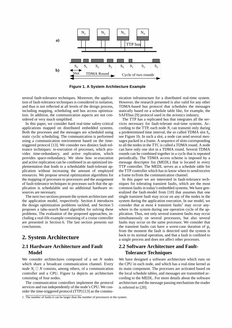
We consider architectures composed of a set N nodeswhich share a broadcast communication channel. Everynode Ni ∈ N consists, among others, of a communicationcontroller and a CPU. Figure 1a depicts an architectureconsisting of four nodes.
The communication controllers implement the protocolservices and run independently of the node’s CPU. We con-sider the time-triggered protocol (TTP) [13] as the commu-
nication infrastructure for a distributed real-time system.However, the research presented is also valid for any otherTDMA-based bus protocol that schedules the messagesstatically based on a schedule table like, for example, theSAFEbus [9] protocol used in the avionics industry.
The TTP has a replicated bus that integrates all the ser-vices necessary for fault-tolerant real-time systems. Ac-cording to the TTP, each node Ni can transmit only duringa predetermined time interval, the so called TDMA slot Si,see Figure 1b. In such a slot, a node can send several mes-sages packed in a frame. A sequence of slots correspondingto all the nodes in the TTC is called a TDMA round. A nodecan have only one slot in a TDMA round. Several TDMArounds can be combined together in a cycle that is repeatedperiodically. The TDMA access scheme is imposed by amessage descriptor list (MEDL) that is located in everyTTP controller. The MEDL serves as a schedule table forthe TTP controller which has to know when to send/receivea frame to/from the communication channel.
In this paper we are interested in fault-tolerance tech-niques for tolerating transient faults, which are the mostcommon faults in today’s embedded systems. We have gen-eralized the fault-model from [10] that assumes that onesingle transient fault may occur on any of the nodes in thesystem during the application execution. In our model, weconsider that at most k transient faults1 may occur any-where in the system during one operation cycle of the ap-plication. Thus, not only several transient faults may occursimultaneously on several processors, but also severalfaults may occur on the same processor. We consider thatthe transient faults can have a worst-case duration of µ,from the moment the fault is detected until the system isback to its normal operation, and that a fault is confined toa single process and does not affect other processes.
2.2 Software Architecture and Fault-Tolerance Techniques
We have designed a software architecture which runs onthe CPU in each node, and which has a real-time kernel asits main component. The processes are activated based onthe local schedule tables, and messages are transmitted ac-cording to the MEDL. For more details about the softwarearchitecture and the message passing mechanism the readeris referred to [20].
1. The number of faults k can be larger than the number of processors in the system.
Figure 1. A System Architecture Example
N1 N2 N3 N4
TTP bus
S0 S1 S2 S3 S0 S1 S2 S3
TDMA Round Cycle of two roundsSlot
a)
b)

The error detection and fault-tolerance mechanisms arepart of the software architecture. We assume a combinationof hardware-based (e.g., watchdogs, signature checking)and software-based error detection methods, systematical-ly applicable without any knowledge of the application(i.e., no reasonableness and range checks) [4]. We also as-sume that all faults can be found using such detection meth-ods, i.e., no byzantine faults which need voting on theoutput of replicas for detection. The software architecture,including the real-time kernel, error detection and fault-tol-erance mechanisms are themselves fault-tolerant.
We use two mechanisms for tolerating faults: re-execu-tion and active replication. Let us consider the example inFigure 2, where we have process P1 and a fault-scenarioconsisting of k = 2 faults with a duration µ = 10 ms that canhappen during one cycle of operation. In Figure 2a we havethe worst-case fault scenario for re-execution, when thefirst fault happens at the end of the process P1’s execution.The fault is detected and, after an interval µ, P1 can be re-executed. Its second execution is labeled with P1/2, which,in the worst-case could also experience a fault at the end.Finally, the third re-execution of P1, namely P1/3, will exe-cute without error. In the case of active replication, depict-ed in Figure 2b, each replica is executed on a differentprocessor. Three replicas are needed to tolerate the twopossible faults and, in the worst-case scenario depicted inFigure 2b, only the execution of P1/3 is successful. In addi-tion, we consider a third case, presented in Figure 2c,which combines re-execution and replication for toleratingfaults in a process. In this case, for tolerating the two faultswe use two replicas and one re-execution: the process P1/1,which has P1/2 as a replica, is re-executed.
With active replication, the input has to be distributed toall the replicas. Since we do not consider the type of faultsthat need replica agreement, our execution model assumesthat the descendants of replicas can start as soon as theyhave received the first valid message from a replica. Repli-ca determinism is achieved as a by-product of the underly-ing TTP architecture [16].
3. Application ModelWe model an application A as a set of directed, acyclic, po-lar graphs G(V, E) ∈ A. Each node Pi ∈ V represents oneprocess. An edge eij ∈ E from Pi to Pj indicates that the out-
put of Pi is the input of Pj. A process can be activated afterall its inputs1 have arrived and it issues its outputs when itterminates. The communication time between processesmapped on the same processor is considered to be part ofthe process worst-case execution time and is not modeledexplicitly. Communication between processes mapped todifferent processors is performed by message passing overthe bus. Such message passing is modeled as a communi-cation process inserted on the arc connecting the senderand the receiver process.
The combination of fault-tolerance policies to be appliedto each process is given by two functions. FR: V → VR de-termines which processes are replicated. When active rep-lication is used for a process Pi, we introduce severalreplicas into the process graph G, and connect them to thepredecessors and successors of Pi. The second functionFX: V ∪ VR → VX applies re-execution to the processes inthe application, including to the replicas in VR, if necessary,see Figure 2c. Let us denote the tuple <FR, FX> with F .
The mapping of a process graph G is given by a functionM: V ∪ VR → N, where N is the set of nodes in the archi-tecture. For a process Pi ∈ V ∪ VR, M(Pi) is the node towhich Pi is assigned for execution. Each process Pi can po-tentially be mapped on several nodes. Let NPi
⊆ N be theset of nodes to which Pi can potentially be mapped. Weconsider that for each Nk ∈ NPi
, we know the worst-case ex-ecution time CPi
Nk of process Pi, when executed on Nk. Wealso consider that the size of the messages is given.
All processes and messages belonging to a process graphGi have the same period Ti = TGi
which is the period of theprocess graph. A deadline DGi
≤ TGiis imposed on each pro-
cess graph Gi. In addition, processes can have associated in-dividual release times and deadlines. If communicatingprocesses are of different periods, they are combined into ahyper-graph capturing all process activations for the hyper-period (LCM of all periods).
4. Design Optimization ProblemsIn this paper, by policy assignment we denote the decisionwhether a certain process should be re-executed or replicat-ed. Mapping a process means placing it on a particularnode in the architecture.
P1/3
P1/1 P1/2 P1/3
P1/1
P1/2
P1/3
a) Re-execution b) Replication
k = 2
µ= 10 ms
C1 = 30 msP1
N1
N1
N2
N3
P1/1
P1/2
c) Re-executedreplicas
N1
N2
Figure 2. Worst-Case Fault Scenario and Fault-Tolerant Techniques
1. As already noted, the first valid message from the replicas is considered as the input.

There could be cases where the policy assignment deci-sion is taken based on the experience and preferences of thedesigner, considering aspects like the functionality imple-mented by the process, the required level of reliability,hardness of the constraints, legacy constraints, etc. We de-note with PR the subset of processes which the designer hasassigned replication, while PX contains processes which areto be re-executed.
Most processes, however, do not exhibit certain particu-lar features or requirements which obviously lead to re-ex-ecution or replication. Let P be the set of processes in theapplication A. The subset P+ = P \ (PX ∪ PR) of processescould use any of the two techniques for tolerating faults.Decisions concerning the policy assignment to this set ofprocesses can lead to various trade-offs concerning, for ex-ample, the schedulability properties of the system, theamount of communication exchanged, the size of theschedule tables, etc.
For part of the processes in the application, the designermight have already decided their mapping. For example,certain processes, due to constraints like having to be closeto sensors/actuators, have to be physically located in a par-ticular hardware unit. They represent the set PM of alreadymapped processes. Consequently, we denote withP* = P \ PM the processes for which the mapping has not yetbeen decided.
Our problem formulation is as follows:• As an input we have an application A given as a set of
process graphs (Section 3) and a system consisting of aset of nodes N connected using the TTP.
• The fault model is given by the parameters k and µ, whichdenote the total number of transient faults that can appearin the system during one cycle of execution and theirduration, respectively.
• As introduced previously, PX and PR are the sets ofprocesses for which the fault-tolerance policy hasalready been decided. Also, PM denotes the set of already
mapped processes.We are interested to find a system configuration ψ such
that the k transient faults are tolerated and the imposeddeadlines are guaranteed to be satisfied, within the con-straints of the given architecture N.
Determining a system configuration ψ = <F, M, S>means:1.finding a combination of fault-tolerance policies F for
each processes in P+ = P \ (PR ∪ PX);2.deciding on a mapping M for each processes in P* =
P \ PM;3.deriving the set S of schedule tables on each processor
and the MEDL for the TTP.
4.1 Fault-Tolerance Policy AssignmentLet us illustrate some of the issues related to policy assign-ment. In the example presented in Figure 3 we have the ap-plication A1 with three processes, P1 to P3, and anarchitecture with two nodes, N1 and N2. The worst-case ex-ecution times on each node are given in a table to the rightof the architecture. Note that N1 is faster than N2. The faultmodel assumes a single fault, thus k = 1, with a durationµ = 10 ms. The application A1 has a deadline of 140 ms de-picted with a thick vertical line. We have to decide whichfault-tolerance technique to use. In Figure 3 we depict theschedules1 for each node, and for the TTP bus. Node N1 isallowed to transmit in slot S1, while node N2 can use slot S2.A TDMA round is formed of slot S1 followed by slot S2,each of 10 ms length. Comparing the schedules inFigure 3a1 and 3b1, we can observe that using (a1) activereplication the deadline is missed. In order to guarantee thattime constraints are satisfied in the presence of faults, re-execution slacks have to finish before the deadline. Howev-er, using (b1) re-execution we are able to meet the deadline.However, if we consider application A2 with process P3
1. The schedules depicted are optimal.
Figure 3. Comparison of Replication and Re-Execution
N1 N2N1 N2P1
P3
P2
m1
P1
P3
P2
m1
P1
S1
N1
N2
TTP
P1
S2
P2
P2
P3
P3
N1
N2
TTP
P1 P2
m1
m1
S1S2
P3
a1)
b1)
k = 1
µ= 10 ms
k = 1
µ= 10 ms
Re-execution slackfor P1 and P2
P1P2P3
N1 N2
40 504060
5070
P1P2P3
N1 N2
40 504060
5070
Deadline
Missed
Met
P1N1
N2
TTP
P1
P2
P2
N1
N2
TTP
P1 P2 P3
P3
P3
S1S2 m1
m1
m2
m2
S1S2
a2)
b2)
Deadline
Missed
Met
Re-execution slackfor P1, P2 , P3
P1 P3P2
m1 m2P1 P3P2
m1 m2
A2
A1

data dependent on P2, the deadline is missed in Figure 3b2if re-execution is used, and it is met when replication isused as in Figure 3a2.
Note that in Figure 3b1 processes P1 and P2 can use thesame slack for re-execution. Similarly, in Figure 3b2, onesingle slack of size C3 + µ is enough to tolerate one fault inany of the processes. In general, re-execution slacks can beshared as long as they allow a re-execution of processes totolerate faults.
This example shows that the particular technique to use,has to be carefully adapted to the characteristics of the ap-plication. Moreover, the best result is most likely to be ob-tained when both techniques are used together, some
processes being re-executed, while others replicated. Let usconsider the example in Figure 4, where we have an appli-cation with four processes mapped on an architecture oftwo nodes. In Figure 4a all processes are re-executed, andthe depicted schedule is optimal for re-execution.
We use a particular type of re-execution, called transpar-ent re-execution [10], that hides fault occurrences on a pro-cessor from other processors. On a processor Ni where afault occurs, the scheduler has to switch to a contingencyschedule that delays descendants of the faulty process.However, a fault happening on another processor, is notvisible on Ni, even if the descendants of the faulty processare mapped on Ni. For example, in order to isolate node N1from the occurrence of a fault in P1 on node N2, message
Figure 4. Combining Re-execution and Replication
a)
b)
P1
P4
P2 P3
m1 m2
m3
P1
P4
P2 P3
m1 m2
m3
N1
N2 P1
P3
P4
P1
P2
N1
N2
P1
P3
S1S2
P4P2
P1
m2
m1TTP
k = 1
µ= 10 ms
k = 1
µ= 10 ms
P1P2P3
N1 N2
40 506060
8080
P4 40 50
P1P2P3
N1 N2
40 506060
8080
P4 40 50
Deadline
Missed
Met
TTP S1S2 m2S1
P2 P4Contingency
schedule
N1 N2N1 N2
Figure 5. Mapping and Fault-Tolerance
P1N1
N2
TTP
P2
P3
N1
N2
TTP
P1 P2 P3
S1S2 m1
S1S2
k = 1
µ = 10 ms
k = 1
µ = 10 ms
Deadline
Missed
Met
P1
P4
P2 P3
m1 m2
m3 m4
P1
P4
P2 P3
m1 m2
m3 m4
P1P2P3P4
N1 N2
40 X606040
70
X70
P1P2P3P4
N1 N2
40 X606040
70
X70P4
P4
m2
P1N1
N2
TTP
P2
P3
S1S2
P4
m2
m1
a)
b)
c)
k = 0
µ = 0 ms
k = 0
µ = 0 ms
Best mapping withoutconsidering fault-tolerance N1 N2N1 N2

m2 from P1 to P3 cannot be transmitted at the end of P1’sexecution. Message m2 has to arrive at the destination evenin the case of a fault occurring in P1, so that P3 can be acti-vated on node N2 at a fixed start time, regardless of whathappens on node N1, i.e., transparently. Consequently, m2can only be transmitted after a time C1 + µ passes, at theend of the potential re-execution of P1, depicted in grey.Message m2 is delivered in the slot S2 of the TDMA roundcorresponding to node N2. With this setting, using re-exe-cution will miss the deadline. Once a fault happens, thescheduler in N2 will have to switch to a contingency sched-ule, depicted with thick-border rectangles.
However, combining re-execution with replication, as inFigure 4b where process P1 is replicated, will meet thedeadline. In this case, message m2 does not have to be de-layed to mask the failure of process P1. Instead, P2 and P3will have to receive m1 and m2, respectively, from both rep-licas of P1, which will introduce a delay due to the inter-processor communication on the bus.
4.2 Mapping and Bus Access OptimizationFor a distributed system, the communication infrastructurehas an important impact on the mapping decisions [21].Not only is the mapping influenced by the protocol setup,but the fault-tolerance policy assignment cannot be doneseparately from the mapping design task. Consider the ex-ample in Figure 5. Let us suppose that we have applied amapping algorithm without considering the fault-toleranceaspects, and we have obtained the best possible mapping,depicted in Figure 5a. If we apply on top of this mapping afault-tolerance technique, for example, re-execution as inFigure 5b, we miss the deadline. The re-execution has to beconsidered during the mapping process, and then the bestmapping will be the one in Figure 5c which clusters all pro-cesses on the same processor in order to reduce the re-exe-cution slack and the delays due to the masking of faults.
In this paper, we will consider the assignment of fault-tolerance policies at the same time with the mapping ofprocesses to processors. However, to simplify the presenta-tion we will not discuss the optimization of the communi-cation channel. Such an optimization can be performedwith the techniques we have proposed in [19] for non fault-tolerant systems.
5. Design Optimization StrategyThe design problem formulated in the previous section isNP complete. Our strategy is outlined in Figure 6 and hasthree steps:1. In the first step (lines 1–3) we decide very quickly on an
initial bus access configuration B0, and an initial fault-tolerance policy assignment F0 and mapping M0. Theinitial bus access configuration (line 1) is determined byassigning nodes to the slots (Si = Ni) and fixing the slotlength to the minimal allowed value, which is equal to thelength of the largest message in the application. Theinitial mapping and fault-tolerance policy assignmentalgorithm (InitialMPA line 2 in Figure 6) assigns a re-execution policy to each process in P+ and produces amapping for the processes in P* that tries to balance the
utilization among nodes and buses. The application isthen scheduled using the ListScheduling algorithmoutlined in Section 5.1. If the application is schedulablethe optimization strategy stops.
2.The second step consists of a greedy heuristicGreedyMPA (line 4), discussed in Section 5.2, that aimsto improve the fault-tolerance policy assignment andmapping obtained in the first step.
3. If the application is still not schedulable, we use, in thethird step, a tabu search-based algorithmTabuSearchMPA presented in Section 5.2. Finally, thebus access optimization is performed.If after these three steps the application is unschedulable,
we conclude that no satisfactory implementation could befound with the available amount of resources.
5.1 List SchedulingOnce a fault-tolerance policy and a mapping are decided, aswell as a communication configuration is fixed, the pro-cesses and messages have to be scheduled. We use a listscheduling algorithm for building the schedule tables forthe processes and deriving the MEDL for messages.
Before applying list scheduling, we merge the applica-tion graphs into one single merged graph Γ, as detailed in[18], with a period equal to the LCM of all constituentgraphs. List scheduling heuristics are based on priority listsfrom which processes are extracted in order to be sched-uled at certain moments. A process Pi is placed in the readylist L if all its predecessors have been already scheduled.All ready processes from the list L are investigated, and thatprocess Pi is selected for placement in the schedule whichhas the highest priority. We use the modified partial criticalpath priority function presented in [20]. At the same timewith placing processes in the schedule, the messages arealso scheduled using the ScheduleMessage function from[20]. The ListScheduling loops until the ready list L is emp-ty.
During scheduling, re-execution slack is introduced inthe schedule for the re-executed processes. The introduc-tion of re-execution slack is discussed in [10] where the to-tal amount of slack is reduced through slack-sharing, asdepicted in Figure 3b2, where processes P1 to P3 can sharethe same slack for re-execution in the case of a fault.
However, the notion of “ready process” in [10] is differ-ent for us in the case of processes waiting inputs from rep-licas. In that case, a process can be placed in the scheduleas soon as we are certain that at least one valid message hasarrived from a replica. Let us consider the example inFigure 7, where P2 is replicated. In the worst-case fault-
Figure 6. The General Strategy
OptimizationStrategy(A, N) 1 Step 1:B0 = InitialBusAccess(A, N) 2 ψ0 = InitialMPA(A, N, B0) 3 if S0 is schedulable then stop end if 4 Step 2:ψ= GreedyMPA(A, N, ψ0) 5 if S is schedulable then stop end if 6 Step 3:ψ = TabuSearchMPA(A, N, ψ) 7 return ψend OptimizationStrategy

scenario, P2 on processor N1 can fail, and thus P3 has to re-ceive message m2 from the P2 replica on processor N2.Thus, P3 has to be placed in the schedule as in Figure 7a.However, our scheduling algorithm will place P3 as inFigure 7b instead, immediately following P2 on N1. In ad-dition, it will create a contingency schedule for P3 on pro-cessor N1, as depicted in Figure 7b using a rectangle with a
thicker margin. The scheduler on N1 will switch to thisschedule only in the case of an error occurring in P2 on pro-cessor N1. This contingency schedule has two properties.First, P3 starts such that the arrival of m2 from the P2’s rep-lica on N2 is guaranteed. Up to this point, it looks similar tothe case in Figure 7a, where P3 has been started at this timefrom the beginning. However, the contingency schedulehas another important property: although P3’s failure ishandled through re-execution, the contingency schedulewill not contain any re-execution slack for P3. That is be-cause, according to the fault model, no more errors canhappen. Thus, the deadline is met, even if any of the pro-cesses will experience a fault.
5.2 Mapping and Fault-Policy AssignmentFor deciding the mapping and fault-policy assignment weuse two steps, see Figure 6. One is based on a greedy heu-ristic, GreedyMPA. If this step fails, we use in the next stepa tabu search approach, TabuSearchMPA.
Both approaches investigate in each iteration all the pro-cesses on the critical path of the merged application graphΓ, and use design transformations (moves) to change a de-sign such that the critical path is reduced. Let us considerthe example in Figure 8, where we have an application offour processes that has to tolerate one fault, mapped on anarchitecture of two nodes. Let us assume that the currentsolution is the one depicted in Figure 8a. In order to gener-ate neighboring solutions, we perform design transforma-tions that change the mapping of a process, and/or its fault-tolerance policy. Thus, the neighbor solutions generatedstarting from Figure 8a, are the solutions presented inFigure 8b–8e. Out of these, the solution is Figure 8c is thebest in terms of schedule length.
The greedy approach selects in each iteration the bestmove found and applies it to modify the design. The disad-vantage of the greedy approach is that it can “get stuck”into a local optima. To avoid this, we have implemented atabu search algorithm, presented in Figure 9.
The tabu search takes as an input the merged applicationgraph Γ, the architecture N and the current implementation
Figure 7. Scheduling Replica Descendants
k = 1
µ = 10 ms
k = 1
µ = 10 ms
P1P2P3
N1 N2
40 408050
8050
P1P2P3
N1 N2
40 408050
8050
P1
P3
P2
m1
m2
P1
P3
P2
m1
m2N1
N2
TTP
P1 P3
S1S2 S2 m1
P2
P2
S1 m2
P3
b)
N1
N2
TTP
P1 P3P2
P2
S1S2 S2 m1 S1 m2
a)
N1
N2
TTP
P1 P3P2
P2
S1S2 S2 m1 S1 m2
a)
Deadline
Missed
Met
N1 N2N1 N2
N1
N2
TTP
P1
P3
S1S2 S2
P4
m2
P2
1101Wait
0021Tabu
P4P3P2P1
1101Wait
0021Tabu
P4P3P2P1
a)
N1
N2
TTP
P1 P3
S1S2 S2
P4P2
m2
N1
N2
P1
P3
S1S2
P4P2
P1
m2
m1TTP
N1
N2
TTP
P1 P3
S1S2 S2
P4
m2
P2
N1
N2
TTP
P1
P3
S1S2 S2
P4
m2
P2 P3
b)
c)
d)
e)
P1
P4
P2 P3
m1 m2
m3
P1
P4
P2 P3
m1 m2
m3
k = 1
µ = 10 ms
k = 1
µ = 10 ms
P1P2P3
N1 N2
40 506060
7575
P4 40 50
P1P2P3
N1 N2
40 506060
7575
P4 40 50
1200Wait
0012Tabu
P4P3P2P1
1200Wait
0012Tabu
P4P3P2P1
Current solution
1101Wait
0021Tabu
P4P3P2P1
1101Wait
0021Tabu
P4P3P2P1
1101Wait
0021Tabu
P4P3P2P1
1101Wait
0021Tabu
P4P3P2P1
1101Wait
0021Tabu
P4P3P2P1
1101Wait
0021Tabu
P4P3P2P1
Tabu move &worse than best-so-far
Tabu move &better than best-so-far
Non-tabu move &worse than best-so-far
Non-tabu move &worse than best-so-far
N1 N2N1 N2
Figure 8. Moves and Tabu History

ψ, and produces a schedulable and fault-tolerant implemen-tation xbest. The tabu search is based on a neighborhoodsearch technique, and thus in each iteration it generates theset of moves Nnow that can be reached from the current so-lution xnow (line 7 in Figure 9). In our implementation, weonly consider changing the mapping or fault-tolerance pol-icy of the processes on the critical path, denoted with CP inFigure 9. We define the critical path as the path through themerged graph Γ which corresponds to the longest delay inthe schedule table. For example, in Figure 8a, the criticalpath is formed from P1, m2 and P3.
The key feature of a tabu search is that the neighborhoodsolutions are modified based on a selective history of thestates encountered during the search. The selective historyis implemented in our case through the use of two tables,Tabu and Wait. Each process has an entry in this tables. IfTabu(Pi) is non-zero, it means that the process is “tabu”,i.e., should not be selected for generating moves, while ifWait(Pi) is greater than the number of processes in thegraph, |Γ|, the process has waited a long time and should beselected for diversification. Thus, lines 9 and 10 of the al-gorithm, a move will be removed from the neighborhoodsolutions if it is tabu. However, tabu moves are also accept-ed if they are better than the best-so-far solution (line 10).In line 12 the search is diversified with moves which havewaited a long time without being selected.
In lines 14–20 we select the best one out of these solu-tions. We prefer a solution that is better than the best-so-farxbest (line 17). If such a solution does not exist, then wechoose to diversify. If there are no diversification moves,we simply choose the best solution found in this iteration,even if it is not better than xbest. Finally, the algorithm up-
dates the best-so-far solution, and the selective history ta-bles Tabu and Wait. The algorithm ends when a schedulablesolutions has been found, or an imposed time-limit hasbeen reached.
Figure 8 illustrates how the algorithm works. Let us con-sider that the current solution xnow is the one presented inFigure 8a, with the corresponding selective history present-ed to its right, and the best-so-far solution xbest is the one inFigure 4a. The generated solutions are presented inFigure 8b–8e. The solution (b) is removed from the set ofconsidered solutions because it is tabu, and it is not betterthan xbest. Thus, solutions (c)–(e) are evaluated in the cur-rent iteration. Out of these, the solution in Figure 8c is se-lected, because although it is tabu, it is better than xbest. Thetable is updated as depicted to the right of Figure 8c inbold, and the iterations continue with solution (c) as thecurrent solution.
6. Experimental ResultsFor the evaluation of our algorithms we used applicationsof 20, 40, 60, 80, and 100 processes (all unmapped andwith no fault-tolerance policy assigned) implemented onarchitectures consisting of 2, 3, 4, 5, and 6 nodes, respec-tively. We have varied the number of faults depending onthe architecture size, considering 3, 4, 5, 6, and 7 faults foreach architecture dimension, respectively. The duration µof a fault has been set to 5 ms. Fifteen examples were ran-domly generated for each application dimension, thus a to-tal of 75 applications were used for experimental
TabuSearchMPA(Γ, N, ψ) 1 -- given a merged application graph Γ and an architecture N produces a policy 2 -- assignment F and a mapping M such that Γ is fault-tolerant & schedulable 3 xbest = xnow = ψ; BestCost = ListScheduling(Γ, N, xbest) -- Initialization 4 Tabu = ∅; Wait = ∅ -- The selective history is initially empty 5 while xbest not schedulable ∧ TimeLimit not reached do 6 -- Determine the neighboring solutions considering the selective history 7 CP = CriticalPath(Γ); Nnow = GenerateMoves(CP) 8 -- eliminate tabu moves if they are not better than the best-so-far 9 Ntabu = {move(Pi) | ∀ Pi ∈ CP ∧ Tabu(Pi)=0 ∧ Cost(move(Pi)) < BestCost} 10 Nnon-tabu = N \ Ntabu
11 -- add diversification moves 12 Nwaiting = {move(Pi) | ∀ Pi ∈ CP ∧ Wait(Pi) > |Γ|} 13 Nnow = Nnon-tabu ∪ Nwaiting
14 -- Select a solution based on aspiration criteria 15 xnow = SelectBest(Nnow); 16 xwaiting = SelectBest(Nwaiting); xnon-tabu = SelectBest(Nnon-tabu) 17 if Cost(xnow) < BestCost then x = xnow -- select xnow if better than best-so-far 18 else if ∃ xwaiting then x = xwaiting -- otherwise diversify 19 else x = xnon-tabu -- if no better and no diversification, select best non-tabu 20 end if 21 -- Perform selected move 22 PerformMove(x); Cost = ListScheduling(Γ, N, x) 23 -- Update the best-so-far solution and the selective history tables 24 If Cost < BestCost then xbest = x; BestCost = Cost end if 25 Update(Tabu); Update(Wait) 26 end while 27 return xbest
end TabuSearchMPA
Figure 9. The Tabu Search Algorithm

evaluation. We generated both graphs with random struc-ture and graphs based on more regular structures like treesand groups of chains. Execution times and message lengthswere assigned randomly using both uniform and exponen-tial distribution within the 10 to 100 ms, and 1 to 4 bytesranges, respectively. The experiments were done on SunFire V250 computers.
We were first interested to evaluate the proposed optimi-zation strategy in terms of overheads introduced due tofault-tolerance. Hence, we have implemented each applica-tion, on its corresponding architecture, using the Optimiza-tionStrategy (MXR) strategy from Figure 6. In order toevaluate MXR, we have derived a reference non-fault toler-ant implementation, NFT. The NFT approach is an opti-mized implementation similar to MXR, but we haveremoved the moves that decide the fault-tolerance policyassignment. To the NFT implementation thus obtained, wewould like to add fault-tolerance with as little as possibleoverhead, and without adding any extra hardware resourc-
es. For these experiments, we have derived the shortestschedule within an imposed time limit: 10 minutes for 20processes, 20 for 40, 1 hour for 60, 2 hours and 20 min. for80 and 5 hours and 30 min. for 100 processes.
The first results are presented in Table 1a, where we havetwo columns, the first column presents the average over-heads introduced by MXR compared to NFT, while the sec-ond column presents the minimum overhead. Let δMXR andδNFT be the schedule lengths obtained using MXR and NFT,respectively. The overhead is defined as 100 × (δMXR –δNFT) / δNFT. We can see that the overheads due to fault-tol-erance grow with the application size. MXR approach canoffer fault-tolerance within the constraints of the architec-ture at an average overhead of approximately 100%. How-ever, even for applications of 60 processes, there are caseswhere the overhead is as low as 52%.
We were also interested to evaluate our MXR approachin the case the number of faults and their length varies. Wehave considered applications with 60 processes mapped onfour processors, and we have varied the number k of faults
MR and SFX
Figure 10. Comparison of MXR with MX, MR and SFX
0
10
20
30
40
50
60
70
80
90
100
20 40 60 80 100
MRSFXMX
0
10
20
30
40
50
60
70
80
90
100
20 40 60 80 100
MRSFXMX
Number of processes
Avg
.% d
evia
tion
from
MX
R
Table 1. Overheads of MXR compared to NFT
(a) Application size (b) Number of faults60 procs., µ=5
(c) µ20 procs., k=3
procs. k % max % avg. % min k % max % avg. % min µ % max % avg. % min
20 3 98.36 70.67 48.87 2 52.44 32.72 19.52 1 78.69 57.26 34.29
40 4 116.77 84.78 47.30 4 110.22 76.81 46.67 5 95.90 70.67 48.87
60 5 142.63 99.59 51.90 6 162.09 118.58 81.69 10 122.95 89.24 67.58
80 6 177.95 120.55 90.70 8 250.55 174.07 117.84 15 132.79 107.26 75.82
100 7 215.83 149.47 100.37 10 292.11 219.79 154.93 20 149.01 125.18 95.60
from 2, 4, 6, 8, to 10, using a constant µ = 5 ms. Table 1bshows that the overheads increase substantially as the num-ber of faults that have to be tolerated increase. This is to beexpected, since we need more replicas and/or re-executionsif there are more faults. Similarly, we have kept the numberof faults constant to 3, and varied µ: 1, 5, 10 15 and 20 ms,for 20 processes and two processors. We can observe in Ta-ble 1c that the overhead also increases with the increase infault duration. However, the increase due to the fault dura-tion is significantly lower compared to the increase due tothe number of faults.
As a second set of experiments, we were interested toevaluate the quality of our MXR optimization approach.Thus, together with the MXR approach we have also eval-uated two extreme approaches: MX that considers only re-execution, and MR which relies only on replication for tol-erating faults. MX and MR use the same optimization ap-proach as MRX, but besides the mapping moves, theyconsider assigning only re-execution or replication, respec-tively. In Figure 10 we present the average percentage de-viations of the MX and MR from MXR in terms ofoverhead. We can see that by optimizing the combinationof re-execution and replication, MXR performs much bet-ter compared to MX and MR. On average, MXR is 77%and 17.6% better than MR and MX, respectively. There arealso situations, for graphs with 60 processes, for example,where MXR is able to reduce the overhead with up to 40%compared to MX, and up to 90% compared to MR. Thisshows that considering re-execution at the same time withreplication can lead to significant improvements.
In Figure 10 we have also presented a straightforwardstrategy SFX, which first derives a mapping without fault-tolerance considerations (using MXR without fault-toler-ance moves) and then applies re-execution. This is a solu-tion that can be obtained by a designer without the helpwith our fault-tolerance optimization tools. We can see thatthe overheads thus obtained are very large compared toMXR, up to 77% more on average. This shows that the op-timization of the fault-tolerance policy assignment has tobe addressed at the same time with the mapping of func-tionality. In Figure 10 we also see that replication (MR) isworst than even the straightforward re-execution (SFX).However, by carefully optimizing the usage of replicationalongside re-execution (MXR), we are able to obtain re-sults that are significantly better than re-execution only(MX).
Finally, we considered a real-life example implementinga vehicle cruise controller (CC). The process graph thatmodels the CC has 32 processes, and is described in [18].The CC was mapped on an architecture consisting of threenodes: Electronic Throttle Module (ETM), Anti-lockBreaking System (ABS) and Transmission Control Module(TCM). We have considered a deadline of 250 ms, k = 2 andµ = 2 ms.
In this setting, the MRR produced a schedulable fault-tolerant implementation with a worst-case system delay of229 ms, and with an overhead compared to NFT of 65%. Ifonly one policy is used for fault-tolerance, as in the case ofMX and MR, with 253 and 301 ms, respectively, the dead-line is missed.
7. ConclusionsIn this paper we have addressed the optimization of distrib-uted embedded systems for fault-tolerance hard real-timeapplications. The processes are scheduled with static cyclicscheduling, while for the message transmission we use theTTP. We have employed two fault-tolerance techniques fortolerating faults: re-execution, which provides time-redun-dancy, and active replication, which provides space-redun-dancy.
We have implemented a tabu search-based optimizationapproach that decides the mapping of processes to the ar-chitecture and the assignment of fault-tolerance policies toprocesses. Our main contribution is that we have consid-ered the interplay of fault-tolerance techniques for reduc-ing the overhead due to fault-tolerance. As our experimentshave shown, by carefully optimizing the system implemen-tation we are able to provide fault-tolerance under limitedresources.
References[1] A. Bertossi, L. Mancini, “Scheduling Algorithms for
Fault-Tolerance in Hard-Real Time Systems”, RealTime Systems Journal, 7(3), 229–256, 1994.
[2] A. Burns et al., “Feasibility Analysis for Fault-TolerantReal-Time Task Sets”, Proceedings of EighthEuromicro Workshop on Real-Time Systems, 29–33,1996.
[3] P. Chevochot, I. Puaut, “Scheduling Fault-TolerantDistributed Hard-Real Time Tasks Independently of theReplication Strategies”, Sixth International Conferenceon Real-Time Computing Systems and Applications,356–363, 1999.
[4] V. Claeson, S. Poldena, J. Söderberg, “The XBWModel for Dependable Real-Time Systems”,Proceedings of International Conference on Paralleland Distributed Systems, 1998.
[5] C. Dima et al, “Off-line Real-Time Fault-TolerantScheduling”, Proceedings of Ninth EuromicroWorkshop on Parallel and Distributed Processing, 410–417, 2001.
[6] G. Fohler, “Joint Scheduling of Distributed ComplexPeriodic and Hard Aperiodic Tasks in StaticallyScheduled Systems”, Proceedings of 16th IEEE Real-Time Systems Symposium, 152–161, 1995.
[7] G. Fohler, “Adaptive Fault-Tolerance with StaticallyScheduled Real-Time Systems”, Proceedings of NinthEuromicro Real-Time Systems Workshop, 161–167,1997.
[8] C. C. Han, K. G. Shin, J. Wu, “A Fault-TolerantScheduling Algorithm for Real-Time Periodic Taskswith Possible Software Faults”, IEEE Transactions onComputers, 52(3), 362–372, 2003.
[9] K. Hoyme, K. Driscoll, “SAFEbus”, IEEE Aerospaceand Electronic Systems Magazine, 8(3), 34–39, 1992.
[10]N. Kandasamy, J. P. Hayes, B. T. Murray, “TransparentRecovery from Intermittent Faults in Time-Triggered

Distributed Systems”, IEEE Transactions onComputers, 52(2), 113–125, 2003.
[11]N. Kandasamy, J. P. Hayes B.T. Murray “DependableCommunication Synthesis for Distributed EmbeddedSystems”, Procedeeng of 22nd InternationalConference on Computer Safety, Reliability, andSecurity, Lecture Notes in Computer Science 2788,Springer-Verlag, 275–288, 2003.
[12]H. Kopetz, “Real-Time Systems–Design Principles forDistributed Embedded Applications”, KluwerAcademic Publishers, 1997.
[13]H. Kopets et al., “Distributed Fault-Tolerant Real-TimeSystems: The Mars Approach”, IEEE Micro, 9(1), 25–40, 1989.
[14]H. Kopetz, Günter Bauer, “The Time-TriggeredArchitecture”, Proceedings of the IEEE, 91(1), 112–126, 2003.
[15]C. Pinello, L. P. Carloni, A. L. Sangiovanni-Vincentelli, “Fault-Tolerant Deployment of EmbeddedSoftware for Cost-Sensitive Real-Time Feedback-Control Applications”, Design, Automation and Test inEurope Conference and Exhibition, 1164–1169, 2004.
[16]S. Poldena, “Fault Tolerant Systems–The Problem of
Replica Determinism”, Kluwer Academic Publishers,1996.
[17]Y. Zhang, K. Chakrabarty, “Energy-Aware AdaptiveCheckpointing in Embedded Real-Time Systems”,Design, Automation and Test in Europe Conference andExhibition, 918–923, 2003.
[18]P. Pop, “Analysis and Synthesis of Communication-Intensive Heterogeneous Real-Time Systems”, Ph. D.Thesis No. 833, Dept. of Computer and InformationScience, Linköping University, 2003.
[19]P. Pop, P. Eles, Z. Peng, “Schedulability Analysis andOptimization for the Synthesis of Multi-ClusterDistributed Embedded Systems”, Design, Automationand Test in Europe Conference and Exhibition, pp. 184-189, 2003.
[20]P. Eles et al., “Scheduling with Bus AccessOptimization for Distributed Embedded Systems”,IEEE Transactions on VLSI Systems, 8(5), 472-491,2000.
[21]P. Pop et al., “Design Optimization of Multi-ClusterEmbedded Systems for Real-Time Applications”,Design, Automation and Test in Europe Conference andExhibition, pp. 1028-1033, 2004.

Global Block RAM Allocation and Accesses for FPGA Implementation of Real-Time Video Processing Systems
Najeem Lawal
Electronic Design Division, Department of Information Technology & Media, Mid Sweden University, SE-851 70, Sundsvall, Sweden
Abstract
FPGA offers the potential to become a reliable, and high-performance reconfigurable platform for the implementation of real-time video processing systems. To utilize the full processing power of FPGA for video processing applications, optimization of memory allocation architecture and memory accesses are important issues. This paper presents an algorithm for the allocation of on-chip FPGA Block RAMs for the implementation of Real-Time Video Processing Systems and two approaches, base pointer approach and distributed pointer approach, to implement accesses to on-chip FPGA Block RAMs. The effectiveness of the algorithm is shown through the implementation of realistic image processing systems. The algorithm, which is based on a heuristic, seeks the most cost effective way of allocating memory objects to the FPGA Block RAMs. The experimental results show that the algorithm generates results which are close to the theoretical optimum for most design cases. A comparison of the two memory accessing approaches on realistic image processing systems design cases also is presented. Results show that compared to the base pointer approach, the distributed pointer approach increases the potential processing power of FPGA, as a reconfigurable platform for video processing systems.
1 Introduction
In a Real-Time Video Processing System (RTVPS), the operations performed on each pixel are often neighbourhood oriented [1]. A neighbourhood of pixels is an operation window about a point in the image and is usually a square or rectangular sub-image about that point. These pixels act as input data on which operations are performed to yield a pixel that corresponds to the central neighbourhood pixel in the output image. The neighbourhood is formed for each pixel in the input image to produce an output image. One consequence of this is that a large amount of data is required to be buffered depending on the size of the video frame and the operation window. The data flow dependencies require data to be stored in buffers, where each buffer normally corresponds to a row in the video frame. The size of each element in this buffer depends on the dynamic range of the video signal. In addition, the dimensions of the process window affect the number of buffers required for the process operation. For a 5x5 window, four line buffers are required while two line buffers are required for a 3x3 window.
Due to its high processing capability, FPGA is an acceptable alternative for implementing high speed, real-time, computation-intensive operations, as in the case of RTVPS [2]. Also, the on-chip memories of an FPGA allow frequently accessed data to be stored close to the data path, thus eliminating the overheads associated with data fetches to external memory.
The available FPGAs on-chip memories are limited and organised as Block RAMs and distributed RAMs. Distributed RAMs are built from the logic resources and are ideal for register files closely integrated with logic. The Block RAMs are more suited to larger on-chip memory storage requirements, such as buffers and caches. For Xilinx FPGA, each Block RAM is a configurable, synchronous block of memory [3, 4]. Additionally, it is also possible to configure each Block RAM as a single- or dual-port memory. For the dual port configuration, the two data ports permit independent synchronous read/write access to the common Block RAM. In addition, the data path widths at each port are independent of each other. Examples of allowable data path widths at each data port for Spartan 3 are 1, 2, 4, 8 (9), 16 (18) and 32 (36) [4]. The values shown in brackets are available when parity bits are used for data storage.

2 Related Works
Attempts at optimising energy consumption, total area and availability of data from the memory subsystems of FPGA and DSP have attracted many research efforts [5 - 7]. This could be explained by the work of Balasa et al. who state that the area occupied and the power consumed by the memory subsystems are up to ten times larger than that of the data-path [8]. Memory accesses are a major contributor to the power consumption for RTVPS. In addition, latency in memory accesses affects the throughput of the RTVPS. Effective optimisation can be achieved through efficient memory architecture and addressing procedure.
There are several approaches available for the development of methods for the efficient handling of data storage and memory transfers. Data Transfer and Storage Exploration (DTSE) is a methodology that supports analysis and optimization of data dominated applications [9]. ATOMIUM is a tool that supports DTSE and can take a DSP algorithm all the way from high-level specification to customized hardware and processor level implementations. The main focus throughout all the design steps is towards memory usage and transactions. In DTSE, the search within a complete design space for an optimal implementation is performed in well-defined steps. The allocation of these steps in the search trajectory is based on heuristics.
Weinhardt and Luk present a technique that optimally allocates memory objects to a set of background memory banks using Integer Linear Programming (ILP) [10]. This technique achieves optimisation by parallelisation of data accesses through pipelining. The optimisation technique cannot distribute a single memory object over several memory banks. Thus, each single ported memory bank is required to be sufficiently large to hold each memory object. Consequently, all accesses to each memory object must be serialised.
The MeSA algorithm is based on the clustering of array variables to determine the memory configuration that will result in the minimum total memory area [11]. The number of memory modules, the size of each module, the number of ports for each module and the grouping of a set of input array variables are computed. The number of ports is balanced for serialized memory accesses within a control and data flow graph. This algorithm cannot however be considered for implementing RTVPS on FPGA. This is because large array variables cannot be distributed among a set of memory modules.
A general approach to FPGA memory allocation and assignment is presented by Gokhale et al. [12] This approach starts from C code, for which the presented method allocates both external and internal memories. Automatic partitioning of a single array among different memories is however not covered by this work.
Jaewon et al. propose a schedule based memory allocation, which allows non-uniform access speeds among memory ports [13]. This heuristic considers latency constraints at the scheduling stage and exploits DRAM page mode accesses at both the array clustering and assignment phases. Gebotys considers scheduling both the register and memory accesses among different control steps [14]. The optimization goal is low energy and is achieved using a network flow model.
None of the allocation algorithms mentioned in this section can fully utilize the FPGA architectures in combination with RTVPS [17]. Either it is not possible to use a fine-grained set of memories, or the algorithms are too complicated as they include the scheduling of serialized accesses. None of the mentioned allocation algorithms can utilize the configurable port data widths supported by the FPGA architectures. This is our motivation for presenting a new memory architecture- and application specific allocation algorithm that can fully utilize the combination of FPGAs and RTVPS.
The work presented by Doggett el al. for memory accessing is optimal where large numbers of memory banks are used as is typical in volume rendering in medical applications [5]. The address generation scheme by Grant, el al. is an efficient option for accessing data with addresses within the power range of two [6]. The scheme uses a register and optionally an offset, to the specify memory read/write addresses.
The memory exploration algorithm in [7] implements memory allocation and array-mapping to RAMs through tight links to the scheduling effect and non-uniform access speeds among the RAM ports to achieve near optimal memory area and efficient energy requirement. The algorithm is however complex and the execution time may slow down hardware design and performance. Moreover the exploration targets SRAM and DRAM as opposed to the on-chip FPGA Block RAMs, which are the focus of this paper. Many efficient, often heuristics based, memory optimisation algorithms have been developed similar to those in [9, 10], however, most of these are tailored to be efficient using DSP. Thus a memory access methodology

is required for the FPGA platform which takes advantage of the global memory allocation architecture proposed by O’Nils et al. for RTVPS implementation [17].
Based on the global memory allocation architecture, an allocation algorithm has been developed and implemented to maximize memory usage while minimising the read/write accesses. This algorithm is presented in this paper. This paper also presents an algorithm that generates addresses for the results of the allocation algorithm for the global memory objects proposed in [17] in order to create a hardware description for accessing the allocated memory. Two different approaches and a comparison of these are presented in this paper. This work is intended to be used in the IMEM library of design tools for which the design flow of the memory sub-component is shown in Figure 1 [18]. The result of the Memory Allocation, stage which is information about organisation and allocation of the RTVPS memory objects, serves as the input to the memory access and address generation stage. The contribution of this work is the generation of VHDL code for high performance hardware implementation of memory allocation to FPGA Block RAM and their accesses in RTVPS. This work is also applicable to memory access formulation in general where the target of the design tool is the FPGA platform.
RTVPS Memory Object
FPGA Block RAM
Memory Allocation
Address Generation
VHDL Model
FPGA
Control Signals
Described in Section 5. Described in Sections 3 and 4.
Figure 1. Proposed Design Flow.
3 Architectural Assumptions
For neighbourhood oriented operations in an RTVPS, line buffers (memory objects) are required to store the data of the neighbourhood pixels. Figure 2 shows a 3x3 pixel neighbourhood for which an image processing operator calculates an output value for the central pixel. In a streamed hardware implementation only one operator can use these memory objects and, all the memory objects are used simultaneously in the RTVPS. It is assumed that the memory objects can be grouped together to form a global memory object for the operator. This grouping can be achieved through:
plinesiR wnW �� (1)
where WRi is the width of the Global Memory Object (GMO) for the operator, nlines is the number of required line buffers for an operator and wp is the bit width representing a pixel. The length of the global memory object is equal to those of the memory objects that formed it, i.e. the image width [17].
Line buffer Line buffer
d d d d d d
p11 p12 p13
p21 p23
p31
p22
p32
p33
p33 p32 p31 p23 p22 p21 p13 p12 p11
a)
b) dpixel
Figure 2. Basic architecture for the implementation of line buffers in neighbourhood oriented image processing operations. Part a) shows an example of a 3×3 neighbourhood and b) its implementation.

This architecture is preferable to that proposed by Norell et al. in which each line buffer (memory module) is mapped directly to memory [19]. This preference is because GMOs require a minimal number of required memory entities in comparison to direct mapping architecture. Consequently, the number of memory accesses for an RTVPS operation is minimal for a global memory object.
4 Memory Allocation
A heuristics-based algorithm for efficient allocation of the GMOs, based on the architecture stated above has been developed and implemented. The algorithm creates the GMOs based on Eq. (1) by grouping memory objects required by an operator together in an RTVPS. It partitions the GMOs to ensure that their widths conform to those specified by the FPGA. The algorithm takes advantage of the dual port capabilities of the Block RAMs to achieve optimal allocations and the possibility of allocating a GMO to as many Block RAMs as required. this allocation algorithm is presented in this section.
For every Block RAM available on the FPGA, the algorithm attempts to allocate it a GMO. Final allocation decisions requiring as few Block RAMs as possible are made, based on the allocations offering the least amount of unused memory space on the allocated Block RAMs. Figure 3 depicts a model of the allocation.
M2
R2
Mk
Ri
MK
RI
M1
R1
…
…
…
…
K is number of available Block RAMs Mk
SMk is the size of Mk specified by FPGA
I is number of GMOs Ri to be allocated LRi, WRi and SRi are length, width and size of Ri.
SRi = LRi * WRi
Decision Di, k
of allocating
Ri to Mk
Figure 3. Allocation model.
4.1 Definitions
To find the optimal use of the Block RAM, the allocation algorithm must observe a few definitions and constraints. These are listed as follows: (i) M is the set of all available Block RAM Mk and K is the number of Block RAMs.
� �KkMM k ,...,2,1�� (2)
(ii) SMk is the size of the Block RAM Mk and is specified by the FPGA. For example, in Xilinx Spartan 2E FPGA SMk is 4096 bits [2]. The memory objects allocated to the Block RAM determine the length LMk and width WMk of Mk.
(iii) Wc is the set of all possible datapath widths Wn for Block RAMs on the FPGA. For example, 1, 2, 4, 8, and 16 are allowed on Xilinx Spartan 2E FPGA [2].
� �NnWW nc ,...,2,1�� (3)
(iv) R is the set of all memory objects Ri to be allocated and I is the number of memory objects.
� �IiRR i ,...,2,1�� (4)

(v) The size SRi of memory object Ri is defined as product of the length LRi and data width WRi of the memory object Ri.
RiRiRi WLS �� (5)
(vi) Each global memory object is characterised by a quadruple of op_idRi, LRi, WRi and xRi.
Ri(op_idRi, LRi, WRi, xRi ) (6)
where op_idRi is an identifier for the operator where the memory objects making up the global memory object Ri are defined and xRi is the segment in which a memory object is located on the global memory object after partitioning into units of allowable data widths in Wc.
(vii) If WRi is not a member of Wc, Ri is partitioned into rj partitions such that the width, wR, of each partition is a member of Wc.
� �JjWwxwLidoprR cRRiRiRiRiii i,...,2,1,),,,_( ��� (7)
(viii) Memory object Ri may be allocated to as many Block RAMs as required.
��
��K
kRiRiki SWL
1, (8)
where Li,k is the part of length LRi allocated at Mk.
(ix) Block RAM only supports a maximum of two data ports.
(x) Di,k is the decision to allocate some/ all of the memory objects Ri at Mk.
��
��L
ikiD
1, (9)
(xi) For all Ri in R and Mk in M that form part of the Di,k, the sum of the allocations may not be more than the size of the Block RAM.
��
��I
iiMkRiki SWL , (10)
4.2 Proposed algorithm
The proposed allocation algorithm is presented in Figure 4. In step 1, the algorithm creates global memory objects according to “Eq. (1)”. In step 2, the algorithm ensures that they conform to the allowable port width configuration according to definition vii. This step is captured in a procedure, confugre_global_memory_objects(R), presented below the algorithm in Figure 4. In steps 3 through to 10, the global memory objects are allocated to the Block RAMs according to definitions viii to xi. In steps 11 through to 20, the algorithm finds the optimal use of unallocated memory space in the Block RAM through the second port. This allocation is also in accordance with definitions viii to xi. Steps 5 and 14 handle the partitioning of the global memory objects with respect to length by allocating part of the length of the memory object to the Block RAM until the memory object has been completely allocated. In steps 7 to 9 and 15 to 17, the algorithm estimates the amount of the memory object possible for allocation to the available space on a Block RAM. This amount is used to update the memory object and the Block RAM if the allocation decision is made. In steps 18 to 20, the algorithm finds the memory object which, when allocated to the remaining space on the current Block RAM through port B, yields the optimal use of the Block RAM. The optimal allocation is that for which the unused memory space is minimum, preferably zero.

The Proposed Allocation Algorithm Algorithm: Memory Allocation(R, M) Parameters: R[R
1 … R
I] set of I memory objects;
M[M1 … M
K] set of K Block RAMs;
Return: M[M1 … M
K] set of K Allocated Block RAMs;
{ 1. create global memory object; 2. R := configure_global_memory_objects(R); 3. for M
k := M
1 upto M
K
4. { for Ri := R
1 upto R
I
5. { determine length of Ri to be allocated;
6. determine port on Mk for allocation;
7. Allocate Ri to M
k;
8. update Mk;
9. update Ri;
10. if Mk has been completely used
{ take next Mk;
} 11. else 12. { if no_of_ports on M
k = 1
13. { pair(Ri,M
k.unused) best_alloc;
14. flag := TRUE; 15. for R
j := R
1 upto R
I
16. { determine length of Rj to be allocated
17. temporarily Allocate Rj to M
k;
18. temporarily update Mk;
17. temporarily update Rj; 19. if Mk is completely used
{ Allocate Rjto Mk; flag = FALSE;
take next Mk; }
20. pair(Rj,Mk.unused) temp_alloc; 21. if temp_alloc.second < best_alloc.second { best_alloc := temp_alloc; } } 22. if flag = TRUE
{ Ri := best_alloc.first; Allocate Ri to Mk; update Mk;
update Ri; } } }
} } } Procedure: configure_global_memory_objects(R) Parameters: R[R
1 … R
I] set of I memory objects;
Return: R[R1 … R
I] set of I memory objects;
{ 1. create new set of memory objects New_R; 2. for R
i := R
1 upto R
I
3. { width := Ri.width;
4. if width Wc
5. { segment_id := 1; 6. foreach W
i in W
c
7. { if width � Wi
8. { count_max := width / Wi; // integer division
9. width := width – (Wi � count_max);
10. for count := 1 upto count_max 11. { Mem_Obj temp(W
i, R
i.length, R
i.operator_id);
12. temp.set_segment(segment_id); 13. add temp to new_R; 14. segment_id := segment_id + 1; } } } } 15. else 16. { add R
i to new_R;
} } 17. return new_R; }
Figure 4. The proposed allocation algorithm.

The procedure for configuring the width of the global memory objects, confugre_global_memory_objects(R), is based on definitions (iii) and (vii). In step 1 of the procedure, a container for the set of global memory objects is created. In this procedure, as the global memory objects are configured they are placed in this container. The container is returned in step 17 as the output of the procedure. As the procedure loops through the set of global memory objects in step 2, the width of each global memory object, WRi, is obtained in step 3 and compared in step 4 with Wc. If WRi is not supported by the FPGA, the segment identifier is created in step 5. In steps 6 to 14, Wc is looped through and its members, Wn, are compared with the WRi. This comparison starts from the largest Wn down to the smallest. An appropriate number of times by which WRi is greater than Wn is used in creating segments according to definition vii. WRi is updated and reused until it is reduced to zero. If the FPGA supports WRi, in steps 15 and 16, the object is left un-partitioned and placed in the returned container.
To illustrate the function of the algorithm, if an operator in an RTVPS requires a neighbourhood of 5x5 window with 12-bit gray scale and 640 by 480 frame size as the input video stream this would result in four memory objects each of length L (=640) and width 12 being created. The memory objects would be combined to create a GMO Ri of width 48. Figure 5 depicts this illustration and op_id represents the operator requiring the GMO.
L by 12
L by 12
L by 12
L by 12
L by 48
Ri
op_id = 1
Figure 5. Creating a GMO.
The partitioning and allocation of GMOs are potentially complicated tasks depending on the length and width of GMOs in RTVPS applications and the Block RAM size. Thus an efficient technique for tracking the position of the GMO to be accessed is required. If the GMO in Figure 5 were to be allocated on a Xilinx Spartan 3 FPGA, it would be partitioned into two segments, of widths 32 and 16, since it would be not possible to have a data path width of 48 on a Xilinx Spartan 3 FPGA. In addition, since each Block RAM is 16KBit (excluding the parity feature), the first segment, of width 32, would require 2 Block RAMs, thus creating two partitions. The second segment would require a single partition on a Block RAM. Figure 6 illustrates the organisation of these partitions and their allocations on two Block RAMs. Hence organising a GMO into many segments and partitions for allocation purposes would be usual encounters in RTVPS applications. Implementation of accesses to these GMOs irrespective of their organisation, and the Block RAM constraints is presented in the next section.
640 by 48
op = 1
Allocation
512 by 32
op = 1 seg = 1 par = 1
BR1 Port A
512 by 32
op = 1 seg = 1 par = 1
640 by 16 op = 1 seg = 2 par = 1
128 by 32
op = 1 seg = 1 par = 2
a)
b)
128 by 32
op = 1 seg = 1 par = 2
640 by 16 op = 1 seg = 2 par = 1
BR2 Port B Port A
offset = 320
Figure 6. Organisation and Allocation of a GMO.
5 Address Generation
This work incorporates the generation of addresses for each GMO element. The allocation software ensures that each Block RAM data object knows not only the width and length of the GMO segment allocated to it, and the port used in allocation, but also the hierarchy of its segment in the GMO. In

addition, each partition stores information about the Block RAM to which it is allocated, the port of allocation and its start address on the Block RAM, the GMO and segment to which it belongs.
The advantage of sequential accesses to memory for RTVPS applications can lead to improved memory performance by using pointers that increase incrementally when there are valid pixel values. Using the GMO architecture further reduces the number of such pointers to one per RTVPS operator. The pointers may be implemented by using a single register for each GMO, further referred to as base pointer, or by using a register for each partition in a GMO, further referred to as distributed pointers.
To this end, the results of the memory allocation stage in Figure 1 are imported into the address generation module. From these allocation results, which consist basically of information about the partitions, GMOs are reconstructed, and address spans for each partition in a Block RAM are generated. The start and end addresses of each partition are calculated. Offsets are considered where dual ports are used for the allocation on Block RAMs for different partitions in order to avoid memory overlap. The generated addresses are used to determine the location of each GMO element. The descriptions for accessing the GMO elements using two approaches, namely the base pointer approach and the distributed pointer approach are presented as follows:
5.1 Base Pointer Approach In this approach, a single pointer is used to track the location of the element to be accessed in the GMO.
The pointer starts at zero and increases to one less than the length of the GMO and then resets to zero. Since the memory accesses are clocked, the value of the pointer increases with clocked access to the Block RAM when there are valid data. Address spans for each partition of the GMO are used to determine the relevant Block RAM relating to the element accessed, depending on the value of the pointer. Hence, only the relevant Block RAMs are enabled while the other related Block RAMs are disabled. Figure 7a depicts this approach for a simplified case in which a GMO consists of a single segment with two partitions.
GMO 1 Length = L L = p1 + p2
Partition 1 Length = p1
Partition 2 Length = p2
Base Pointer base = 0 – L - 1
0 p1 - 1 0 p2 - 1
BR 1 BR 2
if base < p1 access BR1 else access BR2
offset
a)
b) For each GMO: � create Address Table from segments and partitions that make up the
GMO to determine when to change Block RAMs among related partitions
� create an incrementable pointer of length �� �L2log which increases when there are valid pixel values
� using Address Table and pointer value activate appropriate Block RAMs and set the values of address signals.
c)
512 by 32
op = 1 seg = 1 par = 1
BR1 Port A
128 by 32
op = 1 seg = 1 par = 2
640 by 16 op = 1 seg = 2 par = 1
BR2 Port B Port A
offset=320
0 � bp � 639 BR2_EN_A = 1 BR2_A_Adr = bp
512 � bp � 639 BR2_EN_B = 1 BR2_EN_B = 0 BR2_B_Adr = offset + bp - 512
0 � bp � 511 BR1_EN_A = 1 BR2_EN_B = 0 BR1_A_Adr = bp
Base Pointer bp = 0 - 639
Figure 7. Base Pointer Approach.

In the figure, partitions p1 and p2 are allocated to Block RAMs BR1 and BR2. In the figure, BR1_EN_A, BR2_EN_A and BR2_EN_B represent the enable signals on port A of BR1, port A of BR2, and port B of BR2 respectively. Likewise, BR1_A_Adr, BR2_A_Adr and BR2_B_Adr are the address signals on port A of BR1, port A of BR2, and port B of BR2 respectively. A Block RAM is enabled or disabled by assigning ‘1’ or ‘0’ to its enable signal.
From Figure 7a, when the value of base is within the span of p1, the appropriate port on BR1 is enabled and accessed while the relevant port on BR2 is disabled. The reverse is the case when base is no longer within the span of p1, i.e. within the span of p2. This simple example could be extended to cases in which more than one segment makes up a GMO and each segment has more than 2 partitions. A formal description of this approach is shown in Figure 7b. Figure 7c depicts the base pointer implementation of the GMO shown in Figure 6.
5.2 Distributed Pointer Approach In this approach, each partition is handled separately, starting with the first partition in a segment. Local
pointers equal in length to the length of each partition are created. As long as the enable signal of Block RAM for a partition is high, memory access is started at its first position using its pointer and continues incrementally when there are valid data until its full length is reached. During this period, the partition ensures its enable signal is re-asserted while the enable signals of the neighbouring partitions of the same segment are kept low. Controls are transferred to the next partition of similar segment when the upper limit of the partition is reached. If however, the partition is the last in the segment, controls are transferred to the first partition. Since the address buses of partitions on Block RAMs provide appropriate bit vectors to cover their entire lengths, they are used as the local pointer. In this approach, the enable signals of all the first partitions are set to high at start-up to ensure that memory accesses start with the first partitions. Figure 8a depicts this approach. A simplified case of a GMO consisting of a single segment with two partitions p1 and p2 allocated on Block RAMs BR1 and BR2 respectively is considered in Figure 8a. The signals in Figure 8 have similar meanings as in Figure 7. Figures 8b and 8c show formal description and implementation of the GMO depicted in Figure 6 using this approach. Since the 640 by 16 partition is the only one in its segment, it is always enabled and the address is reset to 0 when it reaches its the upper limit.

GMO 1 Length = L L = p1 + p2
Partition 1 Length = p1
Partition 2 Length = p2
0 p1 - 1 0 p2 - 1
BR 1 BR 2
offset
a)
For each segment in each GMO: � create Address Table for each partition in the segment � create an incrementable pointer of length �� �p2log which increases
when there are valid pixel data for partitions in the segment � start memory access with the first partition with start address of 0 � enable Block RAM of currently active partition and disable Block
RAMs of related partitions while pointer is less than partition’s length � if pointer of active equals partition’s length less one, reset it to 0,
disable it and enable next (or first partition if this is the last partition).
b)
c) 512 by 32
op = 1 seg = 1 par = 1
BR1 Port A
128 by 32
op = 1 seg = 1 par = 2
640 by 16 op = 1 seg = 2 par = 1
BR2 Port B Port A
offset=320
BR2_EN_A = 1 & BR2_A_Adr < 639 BR2_A_Adr = BR2_A_Adr + 1 BR2_EN_A = 1 & BR2_A_Adr = 639 BR2_A_Adr = 0 BR2_EN_A = 1
BR2_EN_B = 1 & BR2_B_Adr < 127 BR2_EN_B = 1 BR2_EN_B = 0 BR2_B_Adr = BR2_B_Adr + 1 BR2_EN_B = 1 & BR2_B_Adr = 127 BR2_EN_B = 0 BR2_EN_B = 1 BR2_B_Adr = 0
BR1_EN_A = 1 & BR1_A_Adr < 511 BR1_EN_A = 1 BR2_EN_B = 0 BR1_A_Adr = BR1_A_Adr + 1 BR1_EN_A = 1 & BR1_A_Adr = 511 BR1_EN_A = 0 BR2_EN_B = 1 BR1_A_Adr = 0
Figure 8. Distributed Approach.
6 Experimental Results
The work presented in this paper incorporates address generation using the two approaches described above. The allocation algorithm, address generation and VHDL code generation were implemented in C++ which takes FPGA technology files and memory requirements as input. The implementation was simulated using the memory requirements of real-time video processing design cases [17]. The first design case was a spatio-temporal median filter with a neighbourhood of seven frames and two line buffers. Two instances of this design case were considered. The first, (1-1), being a VGA frame with 24-bit RGB pixels and a 640 frame length, while the second, (1-2), was a PAL frame with an 8-bit gray scale pixel and a 708 frame length. The second design case was a machine vision system with a median filter, segmentation and three 1-bit morphological operations. Also, in this design case two instances were considered. The first, (2-1), being an 8-bit gray scale with VGA resolution as the input video stream while the second (2-2) had a 12-bit gray scale with 1.3 MPixel resolution as the input video stream. Table 1 shows the summary of the memory requirements for the design cases considered.
Table 1. Memory requirement for design cases.
Design Case
# Rows Width Length Size (kbit)
Case 1-1 7 2 24 640 210 Case 1-2 7 2 8 708 77.4 Case 2-1 1
1 3
4 1
16
8 19 1
640 256 640
20.0 4.75 30.0
Case 2-2 1 1 3
4 1
16
12 21 1
1300 4096 1300
60.94 84.0
60.94

Tables 2 shows the results obtained using the implementation of the algorithm for allocating the design cases considered on Xilinx Spartan 3 FPGA.
Table 2. Allocation result of the algorithm on Spartan 3.
In the table the theoretical minima Block RAM required for allocation were estimated from equation (11) [17].
���
���
��
BRAMSize
minimalsize
(11)
where Size is the number of bits required by the design case, given in column 6 in Table 1, and the size of BRAM is the numbers of bits in one Block RAM, 16kbit (without parity) for Xilinx Spartan 3 [3]. Table 2 shows that allocation requirements were equal to the minima values apart from two of the design cases. The minimum value is calculated for allocation on a Block RAM with an infinite number of ports. The minimum value however only indicates the effectiveness of the allocation but not its feasibility, since it is not possible to have Block RAMs with an infinite number of ports. The implementation did not consider parity. The parity feature on Xilinx Spartan 3 FPGA increases the available Block RAM size by providing an additional bit for every 8 bits [3]. When taken into consideration the parity bit makes it possible to have width configurations that are multiples of 9-bit on the Block RAM. In this manner, 18Kbits of Block RAM size can be achieved instead of 16Kbits. This parity feature was not considered since it is specific to only some of the Xilinx FPGA families and not all FPGAs have this feature. From Table 2, the non-minimum result of the algorithm in design cases 1-2 and 2-1 is because if a design case has many operators in relation to the total storage requirement and/or the size of each Block RAM, the number of ports on each Block RAM will limit the allocation.
Table 3 shows the resources required to access the allocated memory objects for the design cases in Table 1, the number of Block RAM required for the allocations and the hardware operation frequency for the two approaches. Xilinx Spartan 3 FPGA was the target platform for implementing both of the above approaches.
Table 3. Comparison of the two approaches
6.1 Complexity analysis
In estimating the complexity of the algorithm, the number of available Block RAMs, K, and the number of memory objects, I, after partitioning with respect to their width, play the major roles. Since the algorithm makes one iteration through the sets of Block RAMs and two iterations through the set of memory objects
Design Cases Minima Block RAM % minima Case 1-1 14 14 100 Case 1-2 5 6 120 Case 2-1 4 5 125 Case 2-2 13 13 100
Case 1-1 Case 1-2 Case 2-1 Case 2-2 BP Dist BP Dist BP Dist BP Dist
No. of 4 input LUTs: 653 994 334 356 155 191 560 804
No. of BRAMs: 14 14 6 6 5 5 13 13
Max. Frequency (MHz): 116 186 106 183 140 214 91 173
Frequency Comparison (%): 100 160 100 173 100 153 100 190

as shown in steps 3, 4 and 13 in Figure 4, the allocation algorithm AA is a function of K and I and its complexity could be expressed as
� � �2, IKIKAA ���� (12) The algorithm is thus, at worse, of the third order of the larger of K and I. Implementation costs depend on the representations of the properties of the Block RAMs, memory objects and allocation objects, and the arithmetic and logic operations defined for them.
7 Discussions
Depending on the number of partitions relating to a GMO, address look-up tables are required to set the enable signals and the values of the address signals to the appropriate Block RAMs on which the element of the GMO currently being pointed at is allocated, while also disabling related Block RAMs. In the Base Pointer Approach, these accesses to the Block RAMs are centrally controlled at the GMO level using a pointer. Hence only one set of address look-up tables is required for each GMO. By contrast, in the Distributed Approach, each partition has its separate address look-up table that is unrelated to those of related partitions. The use of a partition’s address look-up table depends on the value of its enable signal. Hence the total number of address look-up tables for one GMO depends on the number of partitions making up the GMO. This is evident by comparing Figures 7c and 8c. The first row of Table 3 confirms this. Thus the Base Pointer Approach yields more efficient use of hardware resources than the Distributed Approach. The differences in resource requirements are however marginal amounting to less than 3% of the available resources, for example, Xilinx Spartan 3 XC3S400 series [3].
Delays associated with the distribution of a single base pointer caused by long delays in the FPGA are eliminated in the Distributed Pointer Approach since each partition has one local pointer. The use of separate address look-up table for each partition in the Distributed Pointer Approach increases the speed of memory accesses and consequently, increases operating frequency. This is because all signals required for memory accesses are calculated simultaneously at the clock edge. As the third row in Table 3 shows, the Distributed Approach yields more rapid access to data than the Base Pointer Approach.
8 Conclusions
In this paper a heuristics based algorithm for allocation of memory objects to on-chip Block RAMs and two approaches for generating addresses to the access memory objects has been presented. The allocation algorithm assumes that memory objects required by an operator in an RTVPS can be grouped together to form global memory objects at the operator level. It also partitions the memory objects to ensure that their widths conform to those specified by the FPGA. The algorithm takes advantage of the dual port capabilities of the Block RAMs to achieve optimal allocations and the possibility of allocating a global memory object to as many Block RAMs as required. The results show of the allocation algorithm requires not more than 100% of the theoretical minimal value for most of the cases. However, minimum allocation cannot be guaranteed for all the cases since such allocation requires an infinite number of ports on a Block RAM.
The accessing approaches make the implementation of accesses to memory data trivial irrespective of their allocation. Two approaches, Base Pointer Approach and Distributed Pointer Approach have been presented and compared with respect to used hardware resources and performance. The results indicate that the Base Pointer Approach requires fewer resources than does the Distributed Pointer Approach. This resource reduction is however marginal when compared to the total capacity of the device. The Distributed Approach is at least 50% faster than the Base Pointer Approach for all the design cases considered.
Hence, employing this allocation algorithm in FPGA Block RAM allocation and the Distributed Approach maximises the use of FPGA Block RAMS and improves the processing power of FPGA as a reconfigurable platform for RTVPS implementation. Additionally, the heuristics nature of the algorithm means its implementation can be optimised for performance, and the automatic generation of addresses and VHDL code will simplify the implementation of real-time video processing systems.
Creating global memory objects greatly reduces the number Block RAMs therefore reducing the number of memory read/write operations required per operation in the real-time video processing system and hence minimising power consumptions in the FPGA.

Reference
[1] Gonzalez, R., and R. Woods, Digital Image Processing, 2nd edition, Addison-Wesley Pub., 2002.
[2] G. Liersch, and C. Dick, “Reconfigurable Gate Array Architectures for Real Time Digital Signal Processing”, Conf. Record of the Twenty-Eighth Asilomar Conf. on Signals, Systems and Computers, Nov 1994, pp 1383 - 1387.
[3] XILINX, Using Block SelectRAM+ Memory in Spartan-II FPGAs, XAPP173 (v1.1), http://www.xilinx.com, Dec 2000.
[4] XILINX, Using Block RAM in Spartan-3 FPGAs, XAPP463 (v1.1.2), http://www.xilinx.com, July 2003.
[5] M. Doggett, and M. Meissner, “A Memory Addressing And Access Design for Real Time Volue Rendering”, Proc of IEEE Int. Symp. on Circt. and Syst. June 1999, pp 344 - 347.
[6] D. Grant, P.B. Denyer, and I. Finlay, “Synthesis of Address Generators”, Digest of Tech. Papers of IEEE Int. Conf on Computer-Aided Design, Nov 1989, pp 116 - 119.
[7] J. Seo, T. Kim, and P.R. Panda, “Memory Allocation and Mapping in High-Level Synthesis - An Integrated Approach”, IEEE Trans. on VLSI Syst. Oct. 2003, pp 928 - 938.
[8] F. Balasa, F. Catthoor, and H.M. Man, “Background memory area estimation for multidimensional signal processing systems,” IEEE Trans. on VLSI Syst. Vol 3, pp. 157 - 172, June 1995.
[9] L. Nachtergaele, F. Catthoor, F. Balasa, F. Franssen, E. D. Greet, H. Samsom and H. D. Man, “Optimization of memory organization and hierarchy for decrease size and power in video and image process systems”, IEEE Int. Workshop on Mem Tech, Design and Testing, Aug 1995, pp. 82 - 87.
[10] M. Weinhardt, and W. Luk, “Memory access optimization for reconfigurable systems.” IEE Proc-Comput. Digi. Tech., vol. 148, no.3 May 2001, pp 105 - 112.
[11] L. Ramachandran, D. D. Gajski, and V. Chaiyakul, “An Algorithm for Array Variable Clustering”, In Proc ,Europ. Des. Test. Conf., Feb.1994, pp. 262 - 266.
[12] M. Gokhale and J. Stone “Automatic Allocation of Arrays to Memories in FPGA Processors With Multiple Memory Banks, in Proc. of the IEEE Symp. on Field-Programmable Custom Machines, 1999, pp. 63-69.
[13] S. Jaewon, K. Taewhan, and P. R. Panda, “Memory allocation and mapping in high-level synthesis – an integrated approach”, IEEE Trans. on Very Large Scale Integration (VLSI) Systems, vol.11, no.5, 2003
[14] C. H. Gebotys, “Low energy memory and register allocation using network flow”, in Proc. of Design Automation Conf., 1997, pp. 435-40
[15] R. Leupers, and P. Marwedel, “Algorithms for Address Assignment in DSP Code Generation”, Digest of Tech. Papers of IEEE/ACM Int. Conf. on Computer-Aided Design, Nov. 1996, pp 109 - 112.
[16] N. Sugino, H. Miyazaki, S. Iimuro, and A. Nishihara, "Improved Code Optimization Method Utilizing Memory Addressing Operation and its Application to DSP Compiler", IEEE International Symposium on Circuits and Systems, May 1996, pp 249 - 252.
[17] M. O’Nils, B. Thörnberg and H. Norell, “A Comparison between Local and Global Memory Allocation for FPGA Implementation of Real-Time Video Processing Systems”, in Proc of IEEE Int. Conf. on Signals and Electronics Systems, Sept 2004.
[18] B. Thörnberg, H. Norell and M. O’Nils, "IMEM: An Object-Oriented Memory- and Interface Modelling Approach for Real-Time Video Processing Systems", Proc. of the ECSI Forum on Design Languages, 2002.
[19] H. Norell, B. Thörnberg and M. O’Nils, "Automatic Hardware Synthesis of Spatial Memory Models for Real-Time Image Processing Systems", Proc. of the 21st Norchip Conf., Riga, Latvia, Nov 2003

FPGA based Surveillance and Control Computer forCustomer Specific Applications
Niklas Lepistö, Mattias O'NilsDepartment of Information Technology and Media
Mid Sweden UniversityHolmg. 10, 85170 Sundsvall, SWEDEN
[email protected], [email protected]
Abstract
The decreasing price/performance ratio of FPGA-tech-nology and the availability of devices with embedded pro-cessors, communication- and high-speed I/O-blocks makesreconfigurable System on Chip (rSoC) based designs moreattractive for each FPGA-generation that reaches the mar-ket. Surveillance and control computers for heavy vehiclesrequire highly adaptable connection capabilities to fit theconnectivity requirements for a certain vehicle, includingseveral video and communication channels. This requireseveral customer specific versions of similar products thatstill needs to fulfill tight cost constraints, which is similarto those found in ordinary automotive industry. This paperdescribes work-in-progress to investigate if a rSoC archi-tecture can offer the price/performance required for the se-lected applications area. This paper identifies the differentresearch aspects involved in the project together with pos-sible problems and opportunities.
1 Introduction
The costs involved in traditional ASIC based SoC de-signs often limits their use to applications for the mass mar-ket where the cost per device is reduced by the large quanti-ties produced [1]. State-of-art FPGA devices provide a wayto increase the integration level of designs without the hugeNRE-costs and slow design process associated with ASICSoC devices [2].
The increasing performance and reducing costs of FPGAdevices has also made FPGA based solutions attractive forapplications where ASICs normally would be used. Theseapplications are usually found in products that are manufac-tured in such quantities where the unit cost would be similarfor both ASIC and FPGA based designs. The choice be-tween the two technologies would have to be based on thethe differences in time to market and resulting product per-formance. The fast design turnaround time of FPGA based
designs reduce time to market significantly compared to anASIC [1]. An FPGA based design would however result ina higher power consumption and reduced speed making itunsuitable for some applications. FPGAs do not provideany possibility to integrate analog components making itnecessary to provide such functionality by additional exter-nal components thus complicating the design, this couldalso entirely rule out an FPGA based solution in some cas-es. The production of an ASIC does usually include a cer-tain risk due to the high cost of design iterations. Even if theunit cost for ASIC and FPGA solutions for a product are ex-pected to be equal, an unexpected design revision could in-crease the unit cost for an ASIC based product significantly.Some FPGA vendors provide a relatively safe path betweenan FPGA based design an a structured ASIC [1]. A struc-tured ASIC provides some advantages such as lower powerconsumption and higher speed compared to FPGAs,. Themost important disadvantage would be the lack of reconfig-urability.
FPGA based designs are an interesting alternative forproducts that may need to be customized for a specific ap-plication. The reconfigurable nature of an FPGA allowschanges to be made in hardware after the product has beenmanufactured. This flexibility could be used to provide asingle hardware platform that can be used for a large num-ber of product configurations which would reduce the pro-duction costs. An FPGA can be used in different ways to in-crease the flexibility of a system. In some cases the entiresystem can be implemented in an FPGA resulting in a rSoCdesign while others would use an FPGA as a reconfigurableco-processor [3] or communication controller [4]. The re-search field of rSoC is very active and a lot of work remainsto be done. This report describes work-in-progress to inves-tigate if a rSoC architecture can offer the price/performancerequired for implementation of a computer system intendedfor heavy vehicles.

2 Target application
During the last years the use of computer systems in ve-hicles has expanded rapidly. Usually these systems are usedfor navigation and to present statistics or data for the differ-ent components in the vehicle. Automotive computers in
Figure 1. Timberjack harvester
tended for heavy vehicles differ slightly from the devicesused in ordinary vehicles. Heavy vehicles such as forest har-vesters and excavators are usually equipped with complextool systems that are controlled by a computer. These toolsare usually exchangeable which provides flexibility for themachines but also increases the requirements on the com-puters intended to control them. A computer for this pur-pose would require a large number of different connectionpossibilities to cover the wide variety of interfaces and busstandards. This would include interfaces normally used inindustrial applications together with the usual interfaces as-sociated with personal computers as well as video inputsused for surveillance cameras. The harsh environmentswhere the computers usually would operate in requires asealed enclosure which complicates cooling of the compo-nents. This increases the importance of a low power con-sumption. Heavy vehicles like harvesters are usually pro-duced in small quantities compared to regular vehicles mak-ing it expensive to design a specific solution for each typeof vehicle. The cost constraints are similar to those found inordinary automotive industry where increased product costscan not be motivated by additional functionality. The in-creased configurability provided by a rSoC based systemcould make it an cost effective alternative for on-boardcomputers intended for use in heavy vehicles.
3 Research challenges
3.1 Product configurabilityBy using a rSoC based design some of the components
that differ between the different versions of a product canbe implemented in the FPGA making them entirely recon-figurable. This does however require a supply of IP-coresfor the components intended to be integrated. The manu-facturers of FPGA devices usually offer a wide variety of
comercial IP-cores. There also exists different open sourcealternatives of varying quality which usually are releasedunder GNU GPL or similar license. This work includes in-vestigation in which parts of a typical embedded systemwould be suitable for integration in a rSoC. The suitabilitywould be based on available IP-cores , FPGA performanceand total cost. The investigation of IP-cores would mainlyfocus on communication controllers that can be used for ex-ternal communication but could also include a comparisonof different soft-core processors.
The inceased flexibility provided by a SoF based designis often limited by hardware. Even though the componentsimplemented in the FPGA are reconfigurable the electricaland physical interface used for external communication maynot provide the same possibilities. Even though FPGAs usu-ally support many different I/O standards there is no supportfor communication standards that are normally used for ex-ternal communication[2]. A communication controller im-plemented in the FPGA would require an electrical interfacefor signal level conversion. The most practical solutionwould be to use an external device which provides a config-urable electrical interface that can be used for a number ofdifferent communication standards. This kind of devicesmay be simple to design for low data rates but with highspeed communication interfaces such as USB 2.0, FireWireor Fast Ethernet the differences in impedance and otherelectrical characteristics would be difficult to manage. Thephysical differences between connectors of different com-munication standards would also be a problem for a config-urable communication device. One method to solve boththese problems would be to use a modular hardware design.A module containing a connector and electrical interface fora specific standard could be attached to an expansion port,which is connected to the FPGA. This would increase thehardware design costs but would still be profitable com-pared to totally customized products. One of the tasks in-volved in this project is to analyze the appropriate level ofFPGA integration for different communication standards.
Figure 2. FPGA based system with configurable communication devices

An FPGA based system could be designed to be dynamical-ly reconfigurable allowing a reconfiguration of hardwareduring operation[5]. This could be practical for systems thatuse hardware implemented audio/video filters or compres-sion algorithms. The hardware requirements for dynamic re-configuration depends on the system design. To make a dy-namically reconfigurable rSoC where all components havebeen implemented in the FPGA, the FPGA would have tobe partially reconfigurable[6]. This would not be required ifthe system has a separate CPU connected to an FPGA.
3.2 Component interconnectionSome research results show that the connection methods
used between the components in ASIC SoC devices are farfrom optimal for implementation in FPGA based designs[7]. Studies has shown that wide data paths in FPGAs arevery power consuming. Up to 60% of the power consump-tion in an FPGA is usually caused by wiring [8]. Industrialapplications are often mounted in sealed enclosures forprotective purposes. This makes it difficult to provide suffi-cient cooling increasing the importance of a low power con-sumption. Some reports indicate that serial serial connectioninterfaces can be an alternative for low speed on-chip com-munication and would reduce the power consumption sig-nificantly[7]. Some studies have also addressed the largewire delays in FPGAs, providing different methods to re-duce and analyze these delays [9][10]. There still remains alot of research in finding interconnection methods that aresuitable for FPGA based designs.
4 Conclusions
Usually FPGA designs can be found in application whereordinary ASIC designs are not a economical option. FPGAtechnology can also be used to reduce production cost byimproving the flexibility of a product. This paper has pre-sented a planned investigation which is to determine if anrSoC based design would be suitable for an on-board com-puter intended for use in heavy vehicles. The investigationalso includes a number of research subjects in the field ofrSoC design that requires more work. Some of the intendedresearch subjects are:
• Investigation of available IP-cores for different commu-nication controllers and soft-core CPUs.
• Analysis of the appropriate level of FPGA integrationfor different communication standards.
• Research in suitable component interconnection meth-ods for FPGA designs.
• Design test applications for dynamic reconfiguration.
References[1] Zahiri, B., “Structured ASICs: opportunities and challenges”,
21st International Conference on Computer Design, 2003.Proceedings.
[2] Xilinx Inc., www.xilinx.com
[3] Luthra, M. Sumit Gupta Nikil Dutt Rajesh Gupta Nico-lau, A. “ Interface synthesis using memory mapping for anFPGA platform” , Proceedings. 21st International Conferenceon Computer Design, 2003.
[4] Donchev, B. Hristov, M. “Implementation of CAN con-troller with FPGA structures”, CAD Systems in Microelec-tronics, 2003. CADSM 2003. Proceedings of the 7th Interna-tional Conference.
[5] Zuim, R.L. Junior, C.J.N.C. Moreira, L.F.E.Fernandes, A.O.da Mata, J.M. da Silva, D.C., Jr. “Dynamic ReconfigurationBehavior Using Generic FPGAs and FPIDs”, Integrated Cir-cuits and Systems Design, SBCCI 2003
[6] Mesquita, D. Moraes, F. Palma, J. Moller, L. Calazans,N., “Remote and partial reconfiguration of FPGAs: tools andtrends”, Parallel and Distributed Processing Symposium,2003. Proceedings. International.
[7] Andy S. Lee, Neil W. Bergmann, “On-chip CommunicationArchitectures for Reconfigurable System-on-Chip” , Proceedings of Field-Programmable Technology (FPT),2003.IEEE
[8] F. Li, D. Chen, L. He, J. Cong “Architectures evaluation forpower-efficient FPGAs”, Proceedings of the ACM Interna-tional Symposium on FPGA, Feb. 2003.
[9] Brown, S. Khellah, M. Vranesic, N., “Minimizing FPGAinterconnect delays”, Design & Test of Computers, IEEE1996
[10] Kannan P., Bhatia D., “Interconnect estimation for FPGAsunder timing driven domains”, 21st International Conferenceon Computer Design, 2003. Proceedings.

1
Volvo Car Corporation
<<<PhD Project Presentation - Design of Electrical Architectures for Safety Cases >>><<<Volvo Car Corporation, Fredrik Törner, ftorner>>>Date: 2005-02-10, Retention Period: 4 years, Security Class:Public, page 1
Design of Electrical Architectures for Safety CasesIndustrial PhD project
Fredrik Törner
Volvo Car Corporation
<<<PhD Project Presentation - Design of Electrical Architectures for Safety Cases >>><<<Volvo Car Corporation, Fredrik Törner, ftorner>>>Date: 2005-02-10, Retention Period: 4 years, Security Class:Public, page 2
Table of contents
• Who I am• Background to the PhD project• PhD project description• Summary and questions
Volvo Car Corporation
<<<PhD Project Presentation - Design of Electrical Architectures for Safety Cases >>><<<Volvo Car Corporation, Fredrik Törner, ftorner>>>Date: 2005-02-10, Retention Period: 4 years, Security Class:Public, page 3
Who I am
• Fredrik Törner• Master of Science in Electrical Engineering, Chalmers
2004- Specialized in the Dependable Computer Systems International Master Program at Chalmers
• Master thesis involved Fault Tolerance in a TTCAN based demonstrator at Volvo Cars
• Worked with Model Based Functional Development at Volvo Cars during the past year.
• Industial PhD student since 7/2 2005 at Volvo Cars
Volvo Car Corporation
<<<PhD Project Presentation - Design of Electrical Architectures for Safety Cases >>><<<Volvo Car Corporation, Fredrik Törner, ftorner>>>Date: 2005-02-10, Retention Period: 4 years, Security Class:Public, page 4
PhD project
• A joint project between Chalmers and Volvo Cars• Supervisors will be:
• Peter Öhman, Chalmers• Per Johannessen, Volvo Cars
• Finance: Volvo Cars, Swedish Automotive Research Program
• Timeplan: 80% research, 20% Volvo Cars other projects during 2005-2009
Volvo Car Corporation
<<<PhD Project Presentation - Design of Electrical Architectures for Safety Cases >>><<<Volvo Car Corporation, Fredrik Törner, ftorner>>>Date: 2005-02-10, Retention Period: 4 years, Security Class:Public, page 5
Background to the PhD project
Volvo Car Corporation
<<<PhD Project Presentation - Design of Electrical Architectures for Safety Cases >>><<<Volvo Car Corporation, Fredrik Törner, ftorner>>>Date: 2005-02-10, Retention Period: 4 years, Security Class:Public, page 6
Challenges, development of automotive electronics
“For 28 percent of our Mercedes owners (and 17 percent of BMW drivers), trouble started on day one…”
“In most cases the culprits could be found somewhere in the electronic network.”
Autocar / Auto motor und sport

2
Volvo Car Corporation
<<<PhD Project Presentation - Design of Electrical Architectures for Safety Cases >>><<<Volvo Car Corporation, Fredrik Törner, ftorner>>>Date: 2005-02-10, Retention Period: 4 years, Security Class:Public, page 7
Future development of automotive systems
• Adaptive Cruise Control, Forward Collision Warning• Electric Parking Brake, Electric Steering Column Lock
• Lane Keeping Aid• Electric Power Assisted Steering, Electro-Hydraulic Brakes
• Collision Avoidance by Braking and by Steering• Brake-by-Wire, Steer-by-Wire
Volvo Car Corporation
<<<PhD Project Presentation - Design of Electrical Architectures for Safety Cases >>><<<Volvo Car Corporation, Fredrik Törner, ftorner>>>Date: 2005-02-10, Retention Period: 4 years, Security Class:Public, page 8
System solution
Vehicle level control
EngineBrakesTrans-
mission SteeringSus-
pensionDiffe-
rentials ISG …
Coordination
Intelligent actuators
Driver/vehicle control & feedback
Volvo Car Corporation
<<<PhD Project Presentation - Design of Electrical Architectures for Safety Cases >>><<<Volvo Car Corporation, Fredrik Törner, ftorner>>>Date: 2005-02-10, Retention Period: 4 years, Security Class:Public, page 9
System solution – implementation today
Vehicle level control
EngineBrakesTrans-
mission SteeringSus-
pensionDiffe-
rentials ISG …
Coordination by message passing
Intelligent actuators
Driver/vehicle control & feedback
Supplier A Supplier B Supplier N…
Volvo Car Corporation
<<<PhD Project Presentation - Design of Electrical Architectures for Safety Cases >>><<<Volvo Car Corporation, Fredrik Törner, ftorner>>>Date: 2005-02-10, Retention Period: 4 years, Security Class:Public, page 10
System solution – implementation future
Vehicle level control
EngineBrakesTrans-
mission SteeringSus-
pensionDiffe-
rentials ISG …
Coordination by distribution of functionality
Intelligent actuators
Driver/vehicle control & feedback
Supplier A Supplier B Supplier N…
Automotive OEM as systemintegrator
Volvo Car Corporation
<<<PhD Project Presentation - Design of Electrical Architectures for Safety Cases >>><<<Volvo Car Corporation, Fredrik Törner, ftorner>>>Date: 2005-02-10, Retention Period: 4 years, Security Class:Public, page 11
Summarized challenges
• Increased complexity in automotive functionality
• Distributed functionality
• Increased interaction between subsystem demands that the OEM will take the role as system integrator.
Volvo Car Corporation
<<<PhD Project Presentation - Design of Electrical Architectures for Safety Cases >>><<<Volvo Car Corporation, Fredrik Törner, ftorner>>>Date: 2005-02-10, Retention Period: 4 years, Security Class:Public, page 12
Legal requirements regarding ”Complex Electronic Vehicle Control Systems”
• A description of the measures designed into the system, for example within the electronic units, so as to address system integrity and thereby ensure safe operation even in the event of an electrical failure
• Safety Case
• Is valid for brake systems today (ECE R13H)• Will soon be valid for steering systems (ECE R79H)

3
Volvo Car Corporation
<<<PhD Project Presentation - Design of Electrical Architectures for Safety Cases >>><<<Volvo Car Corporation, Fredrik Törner, ftorner>>>Date: 2005-02-10, Retention Period: 4 years, Security Class:Public, page 13
Safety
• Safety is a system property and has to be design as such• Safety can be seperated in functional safety and system
safety• System safety implies that the system should not cause a
serious situation
• Safety Cases are related to system safety
Volvo Car Corporation
<<<PhD Project Presentation - Design of Electrical Architectures for Safety Cases >>><<<Volvo Car Corporation, Fredrik Törner, ftorner>>>Date: 2005-02-10, Retention Period: 4 years, Security Class:Public, page 14
Safety Case
• A Safety Case argues that a system is safe and can be used as a statment for product liablility
• Existing legal requirements for Complex Electronic Vehicle Control Systems demands Safety Cases
• A Safety Case can be based on:• Fault analysis such as FMEA, FTA• Reference architectures• Design principles• Development processes• …
Volvo Car Corporation
<<<PhD Project Presentation - Design of Electrical Architectures for Safety Cases >>><<<Volvo Car Corporation, Fredrik Törner, ftorner>>>Date: 2005-02-10, Retention Period: 4 years, Security Class:Public, page 15
Safety Case
Safety Justification for Sub-system
Safety Justification for Sub-system
Safety Justification for Sub-system…
Safety Case for System
System architecture
Systemintegration
Designmethods
Design principles
Volvo Car Corporation
<<<PhD Project Presentation - Design of Electrical Architectures for Safety Cases >>><<<Volvo Car Corporation, Fredrik Törner, ftorner>>>Date: 2005-02-10, Retention Period: 4 years, Security Class:Public, page 16
PhD project description
Volvo Car Corporation
<<<PhD Project Presentation - Design of Electrical Architectures for Safety Cases >>><<<Volvo Car Corporation, Fredrik Törner, ftorner>>>Date: 2005-02-10, Retention Period: 4 years, Security Class:Public, page 17
Research questions
How is a safety case best developed for distributed control systems in the automotive industry?
How can a safety case be developed to support the development of electrical architectures?
Volvo Car Corporation
<<<PhD Project Presentation - Design of Electrical Architectures for Safety Cases >>><<<Volvo Car Corporation, Fredrik Törner, ftorner>>>Date: 2005-02-10, Retention Period: 4 years, Security Class:Public, page 18
Relevance for Volvo
• Swedish automotive industry has high expectations from customers and owners.
• A Safety Case is required to be able to sell cars with electrical controled chassi systems.
• A Safety Case raises the opportunity to increase the system safety in itself through increased awareness.
• Future customer functions requires increased focus on safety.

4
Volvo Car Corporation
<<<PhD Project Presentation - Design of Electrical Architectures for Safety Cases >>><<<Volvo Car Corporation, Fredrik Törner, ftorner>>>Date: 2005-02-10, Retention Period: 4 years, Security Class:Public, page 19
Project deliverables
• Development process for Safety Cases• Integration of Safety Justifications to form a good Safety Case
• Adapted system architecture
• Method for system integration• Definition of fault containing areas• Fault handling at interfaces
Volvo Car Corporation
<<<PhD Project Presentation - Design of Electrical Architectures for Safety Cases >>><<<Volvo Car Corporation, Fredrik Törner, ftorner>>>Date: 2005-02-10, Retention Period: 4 years, Security Class:Public, page 20
Project deliverables cont’
• Designmethods• Risk analysis• Fault analysis methods
• Design principles• Reliable communication• Redundancy• Fault detection
• Case studies for verification and validation of results
Volvo Car Corporation
<<<PhD Project Presentation - Design of Electrical Architectures for Safety Cases >>><<<Volvo Car Corporation, Fredrik Törner, ftorner>>>Date: 2005-02-10, Retention Period: 4 years, Security Class:Public, page 21
Summary and questions
• Safety Cases will be increasingly important for the automotive industry due to legal requirements and more complex systems
• The project goal is to develop a validated process with development methods and design principles for Safety Cases within the automotive area.
• Questions?
Volvo Car Corporation
<<<PhD Project Presentation - Design of Electrical Architectures for Safety Cases >>><<<Volvo Car Corporation, Fredrik Törner, ftorner>>>Date: 2005-02-10, Retention Period: 4 years, Security Class:Public, page 22
Design of Electrical Architectures for Safety CasesIndustrial PhD project
Fredrik Tö[email protected]

ADVANCED COMPONENT-BASED SOFTWARE ENGINEERING COURSE
GUEST LECTURES 2005- 02-23, MDH, ZETA RoomLecture 1: 13:15-15:00 Wolfgang Weck: How is Eclipse Coming Along as a Component Framework?
LEcture 2: 15:15-17:00, Mikael Åkerholm: Real -Time Component-based Echnology: SaveCCM
Wolfgang Weck: How is Eclipse Coming Along as a Component Framework? Eclipse is widely used as an (extensible) IDE. Starting with version 3, it is also advertised as a RichClient Platform (RCP). To what extend is it also a component framework? A component frameworknot only needs to support extension with new components and interaction between them, it shouldalso safeguard developers from certain mistakes that are easily made and hardly detected, ifcomponents are constructed independently and composed later by third parties. We look at thetechnology Eclipse provides but also into the "feature interaction" of component principles and opensource. Dr. Wolfgang Weck is an independent software architect based in Zurich, Switzerland. Besides hisconsulting work he is lecturing at various Universities of Applied Sciences. He has been leadingnumerous consulting and implementation projects and was the product manager of the BlackBoxComponent Builder while working for Oberon microsystems. He has conducted research inprogramming language support for component software and component specification at Åbo Akademi,Turku, Finland, and ETH Zurich, Switzerland. He has presented accepted and invited talks at variousconferences, such as OOPLSA and FMCO and he is one of the co-organizers of the yearly WCOPworkshops.
Mikael Åkerholm: Real-Time Component-based Technology: SaveCCM
This presentation describes a prototype component technology, intended for embedded controlapplications in vehicular systems. The technology has limited flexibility to facilitate future applicationof analysis of imporatant quality attributes in the domain, however, the expressive power has been focused to the needs of vehicular systems. The presentation willconclude with suggestions for student projects related to the technology.
Mikael Åkerholm is a PhD student at MdH/IDE. He received a master’s degree in computer science and engineeringfrom Mälardalen University in 2003, and continued with PhD studies at the same department directly. Mikael hasobtained his licentiate degree "A Software Component Technology for Vehicle Control Systems - Trade-Off BetweenEnginnering Flexibility and Predictability" in 2005. Mikael's research interests are component based softwareengineering, real-t ime, safety-crit ical, and embedded systems. He is part icipating in the SAVE project, which is aresearch project that tries to enable component based software engineering for safety crit ical vehicular systems.
This page has been accessed 46 t imes, Updated: 2005-02-15


