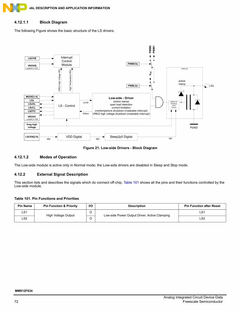
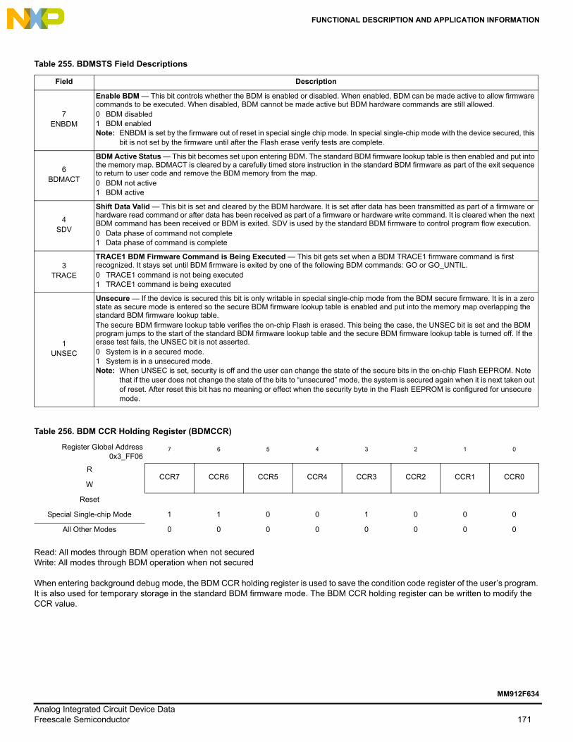
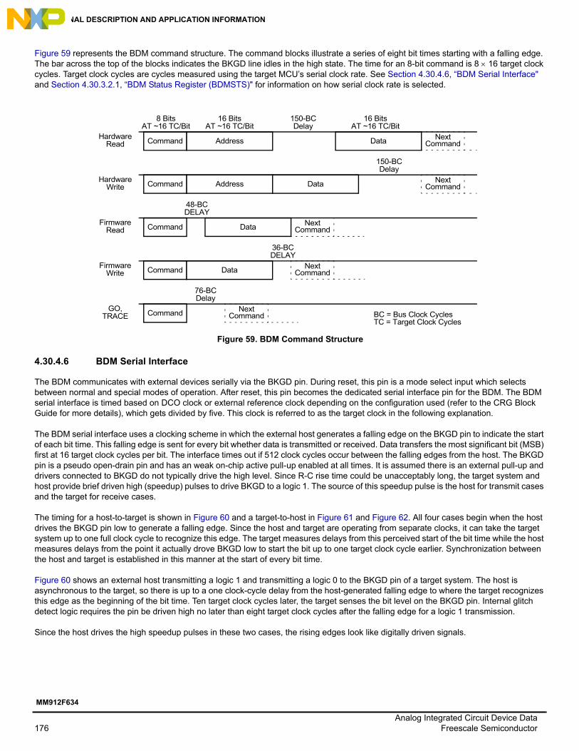
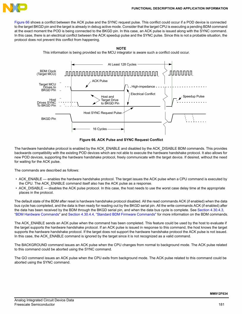
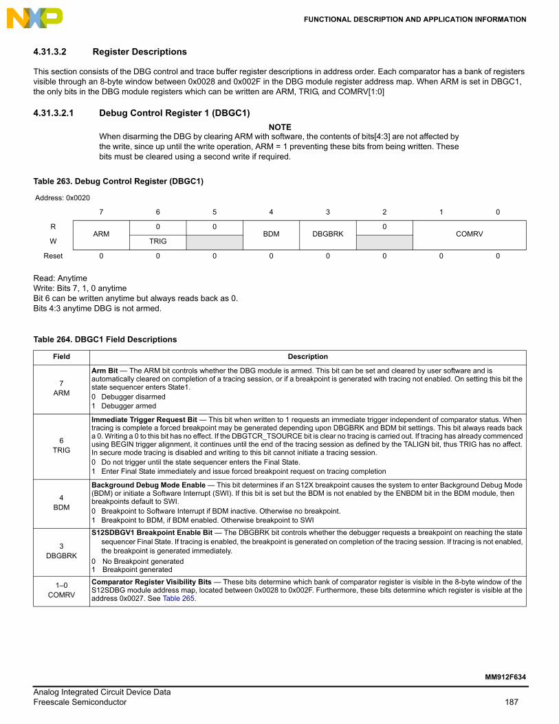
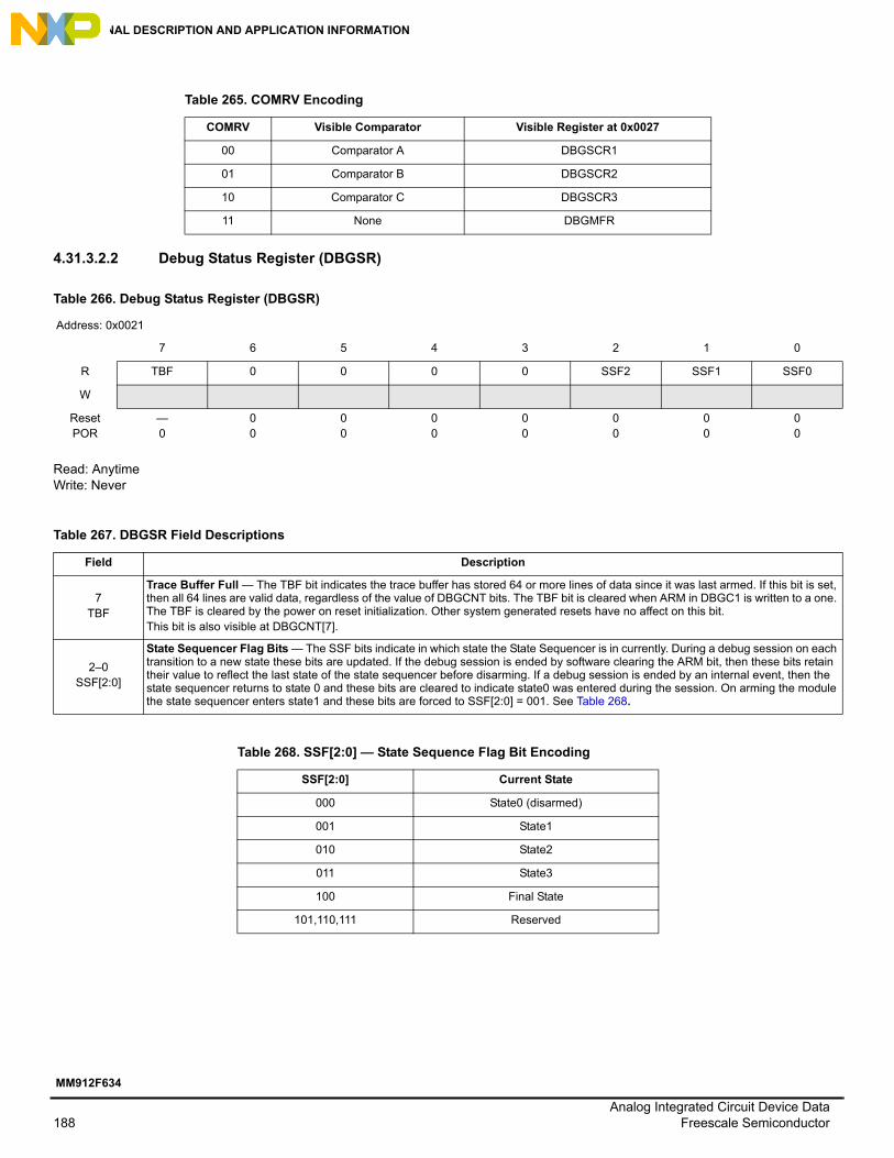
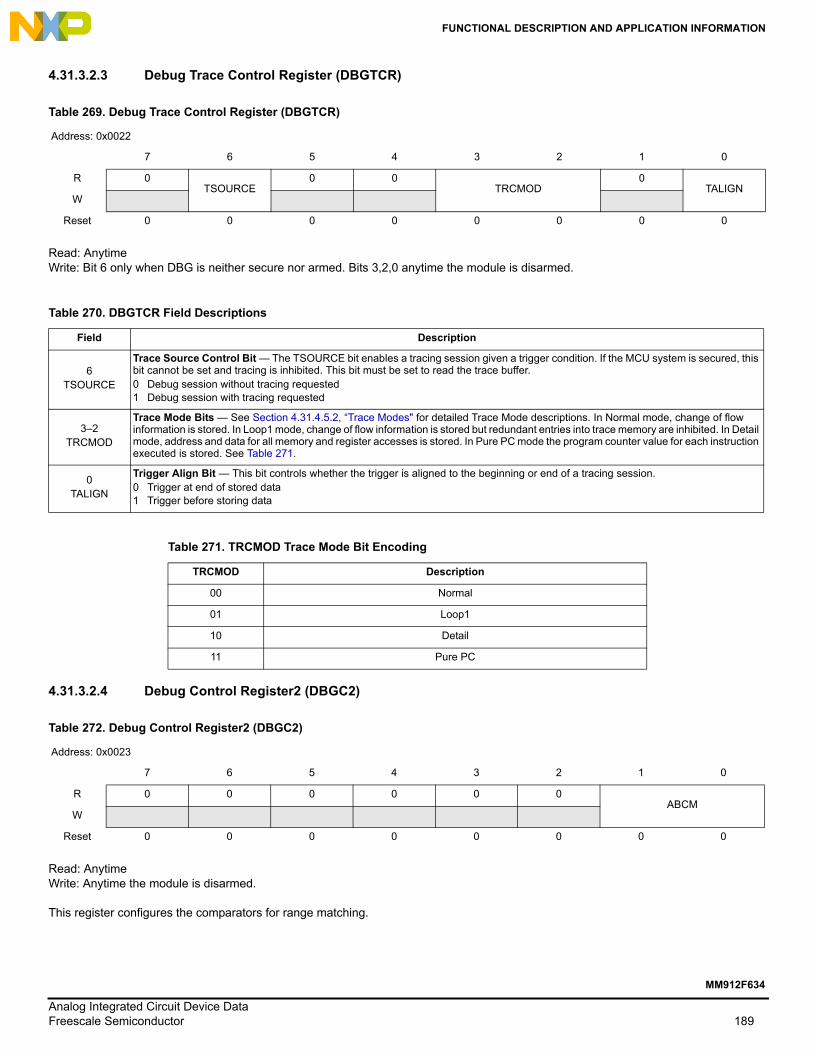
Integrated S12 Based Relay Driver with LINThe MM912F634 is an integrated single package solution integrating an HCS12 microcontroller with a SMARTMOS analog control IC. The Die to Die Interface (D2D) controlled analog die combines system base chip and application specific functions, including a LIN transceiver.
Features
• 16-Bit S12 CPU, 32 kByte FLASH, 2.0 kByte RAM• Background debug (BDM) & debug module (DBG)• Die to die bus interface for transparent memory mapping• On-chip oscillator & two independent watchdogs• LIN 2.1 physical layer interface with integrated SCI• Six digital MCU GPIOs shared with SPI (PA5…0)• 10-Bit, 15 channel - analog to digital converter (ADC) • 16-Bit, four channel - timer module (TIM16B4C)• 8-Bit, two channel - pulse width modulation module (PWM)• Six high-voltage / wake-up inputs (L5.0)• Three low-voltage GPIOs (PB2.0)
• Low-power modes with cyclic sense & forced wake-up• Current sense module with selectable gain• Reverse battery protected voltage sense module • Two protected low-side outputs to drive inductive loads• Two protected high-side outputs• Chip temperature sensor• Hall sensor supply• Integrated voltage regulator(s)
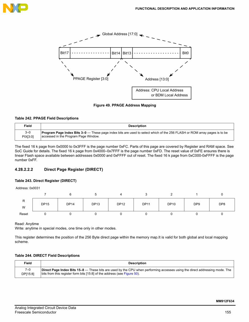
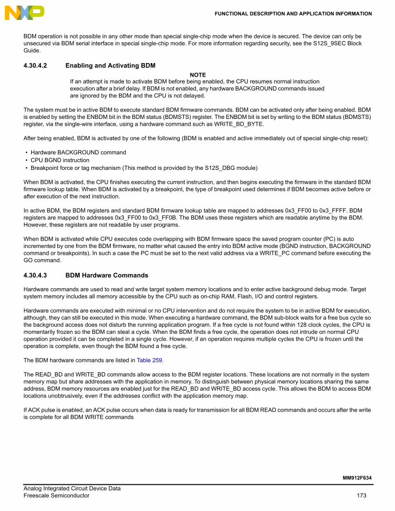
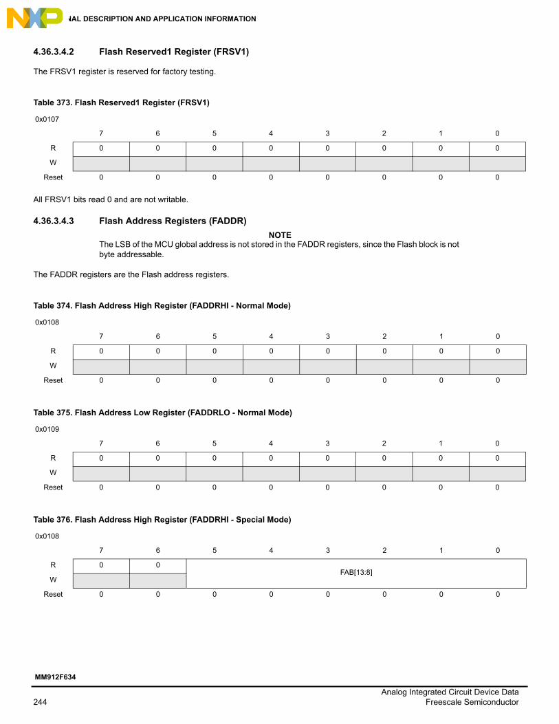
Figure 1. Simplified Application Diagram
MM912F634
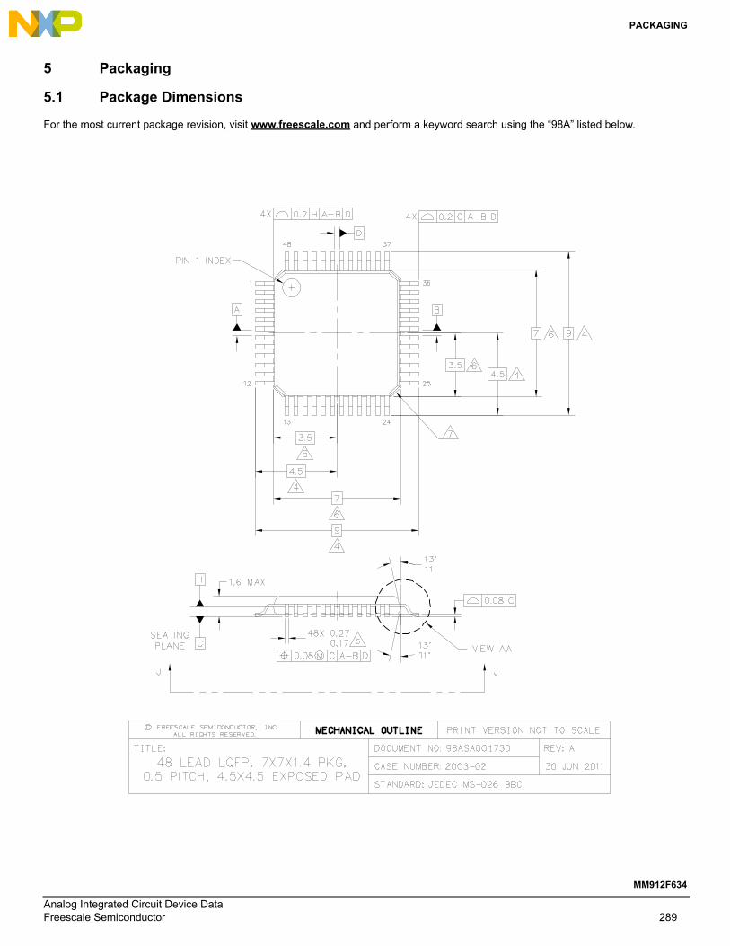
48-PIN LQFP-EP98ASA00173D
7.0 mm x 7.0 mmAE SUFFIX: Exposed Pad
48-PIN LQFP98ASH00962A
7.0 mm x 7.0 mmAP SUFFIX: Non-exposed Pad
M
PA0/MISO
RESET_A
RESET
VDD
EVDD
EVSS
LIN
LS1
LS2
ISENSEH1
VS1Power Supply
LIN interface
5V digital I/O
LGND
ISENSEL1
HSUP
Analog/Digital Inputs
(High Voltage- and Wake Up capable)
DGND
L31
L1
L21
PTB1/AD1/TX/TIM0CH1
PTB2/AD2/PWM/TIM0CH2
Hall Sensor supply
5V GPI/O with optional pull-up (shared with ADC, PWM, Timer, SCI)
The device part number follows the standard scheme below:
Figure 2. Part Number Scheme
Table 1. Ordering Information
Device (2) Temperature Range (TA)
PackageMax. Bus Frequency
(MHz) (fBUSMAX)Flash (kB) RAM (kB)
Analog Option (1)
MM912F634DV1AE
-40 to 105 °C98ASA00173D, 48-PIN LQFP-EP 20 32
2
1
MM912F634DV2AE2
MM912F634DV2AP 98ASH00962A, 48-PIN LQFP 16 32
Note:1. See Table 2.2. For Tape and Reel orders add R2 to the part suffix
Table 2. Analog Options(3)
Feature Option 1 Option 2
Current Sense Module YES NO
Wake-up Inputs (Lx) L0…L5 L0…L3
Note:3. This table only highlights the analog die differences between the derivatives. See Section 4.2.3, “Analog Die Options" for detailed information.
Analog Integrated Circuit Device DataFreescale Semiconductor 3
MM912F634
ORDERING INFORMATION
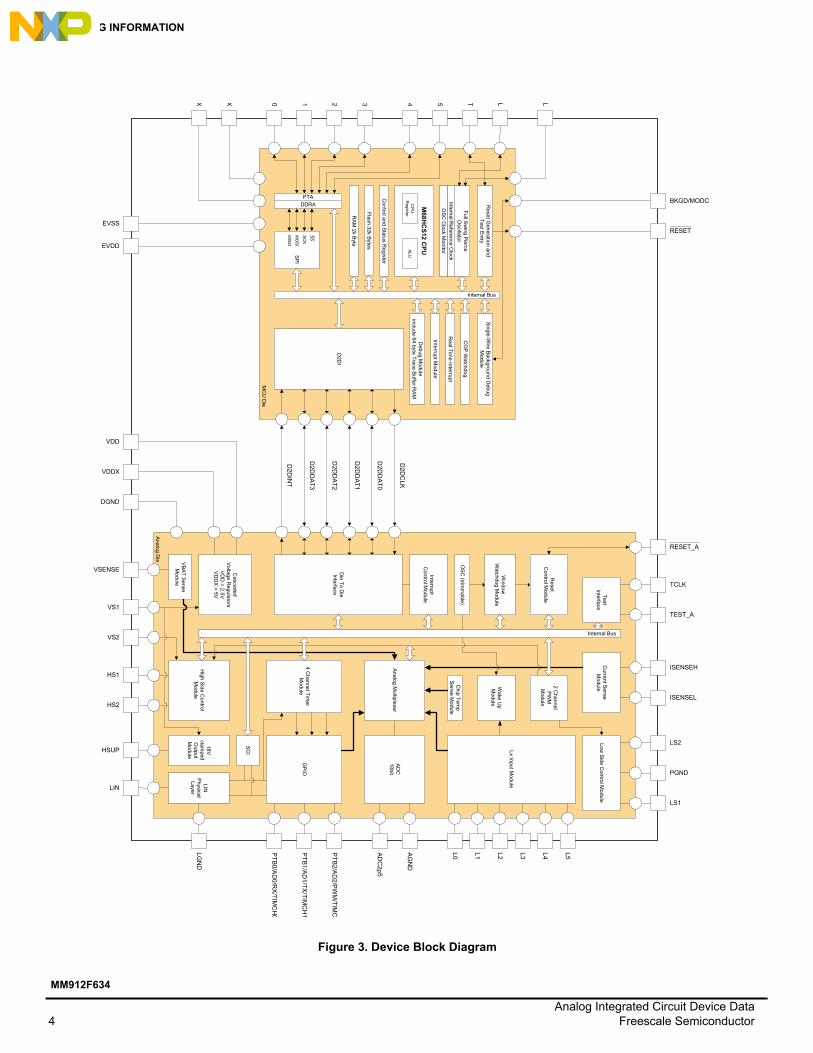
Figure 3. Device Block Diagram
Cascaded
Voltage R
egulatorsV
DD
= 2.5V
VD
DX
= 5V
Die T
o Die
Interface
Reset
Control M
odule
Window
Watchdog M
odule
RESET_A
VS2
AG
ND
18V
clamped
Output
Module
HS1
LS2HSUP
VSENSE
ISENSEL
Lx Input Module
LIN
VS1
D2D
DA
T1
D2D
DA
T0
D2
DC
LK
D2D
INT
Wake U
p M
odule
Current S
ense M
odule
InterruptC
ontrol Module
Low S
ide Control M
odule
VB
AT
Sense
Module
Analog M
ultiplexer
L3L2L1L0
HS2
LS1
ISENSEH
PGND
Chip T
emp
Sense M
odule
High S
ide Control
Module
VDDX
VDD
SC
I
D2D
DA
T3
D2D
DA
T2
OS
C (trim
mable)
AD
C10bit
PT
B1
/AD
1/T
X/T
IMC
H1
GP
IO
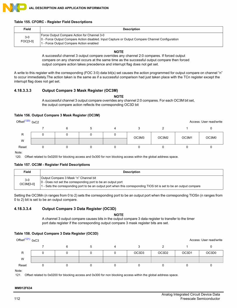
PT
B0
/AD
0/R
X/T
IMC
H0
PT
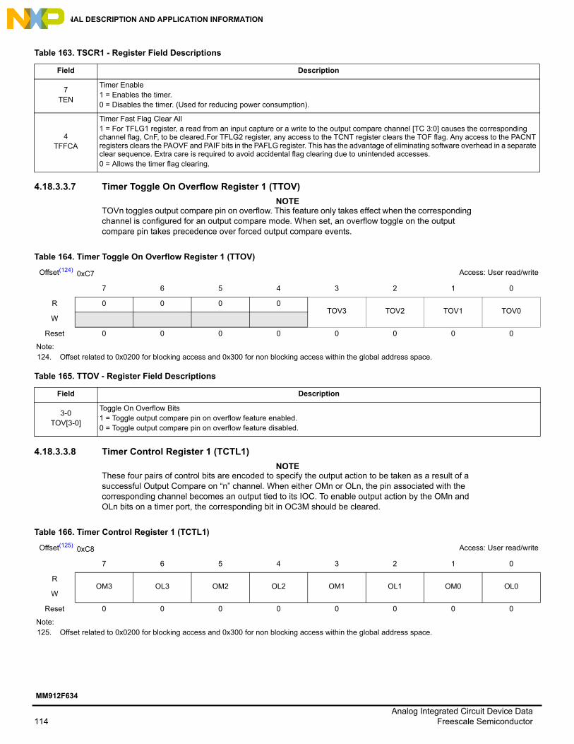
B2
/AD
2/P
WM
/TIM
C
LIN
Physical Layer
Internal Bus
Analog D
ie
Internal Bus
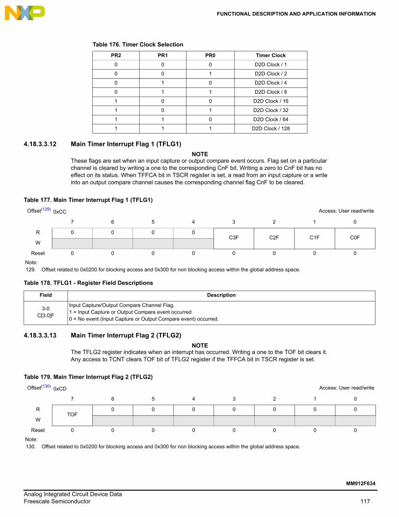
M68
HC
S12 C
PU
CP
UR
eg
ister
AL
U
D2D
I
Control and S
tatus Register
Flash 32k B
ytes
RA
M 2k B
yte
Debug M
odule include 64 byte T
race Buffer R
AM
Reset G
eneration andT
est Entry
Full S
wing P
ierceO
scillator
Internal Reference C
lock
OS
C C
lock Monitor
Single-W
ire Background D
ebug M
odule
CO
P W
atchdog
Real T
ime Interrupt
Interrupt Module
SP
I
DDRA
MO
SI
MIS
O
SC
K
PTA
MC
U D
ie
SS
0 1 2 3 4 5 T L L
BKGD/MODC
RESET
XX
EVSS
EVDD
DGND
L5L4
4 Channel T
imer
Module
AD
C2p
5
LGN
D
Test
Interface
TCLK
TEST_A
2 Channel
PW
MM
odule
Analog Integrated Circuit Device Data4 Freescale Semiconductor
MM912F634
PIN ASSIGNMENT
2 Pin Assignment
Figure 4. MM912F634 Pin Out
NOTEThe device exposed pad (package option AE only) is recommended to be connected to GND.
Not all pins are available for analog die option 2. See Section 4.2.3, “Analog Die Options" for details.
2.1 MM912F634 Pin Description
The following table gives a brief description of all available pins on the MM912F634 package. Refer to the highlighted chapter for detailed information.
Table 3. MM912F634 Pin Description
Pin # Pin Name Formal Name Description
1 NC Not connected Pin This pin is reserved for alternative function and should be left floating or connected to GND.
2 EXTAL MCU Oscillator PinEXTAL is one of the optional crystal/resonator driver and external clock pins. On reset, all the device clocks are derived from the Internal Reference Clock. See Section 4.33, “External Oscillator (S12SOSCFPV1)".
RE
SE
T_
A
1
2
3
4
5
6
7
8
9
10
11
12
NC
EVSSX
EVDDX
EXTAL
XTAL
TEST
PA5
PA4
PA3
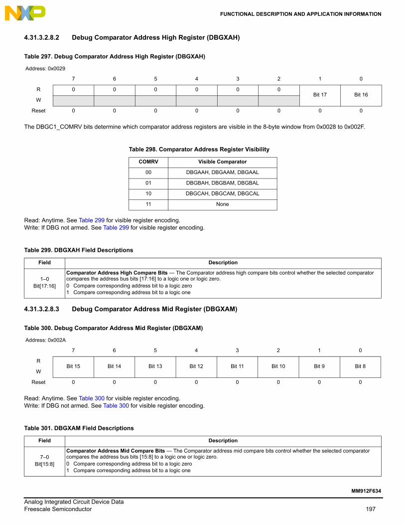
PA2
PA1
PA0
36
35
34
33
32
31
30
29
28
27
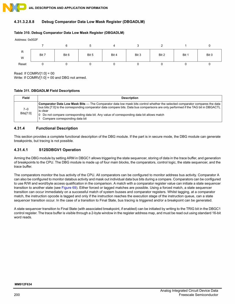
26
25
L5
PTB0
LGND
L4
L3
L2
L1
L0
AGND
ADC2p5
PTB2
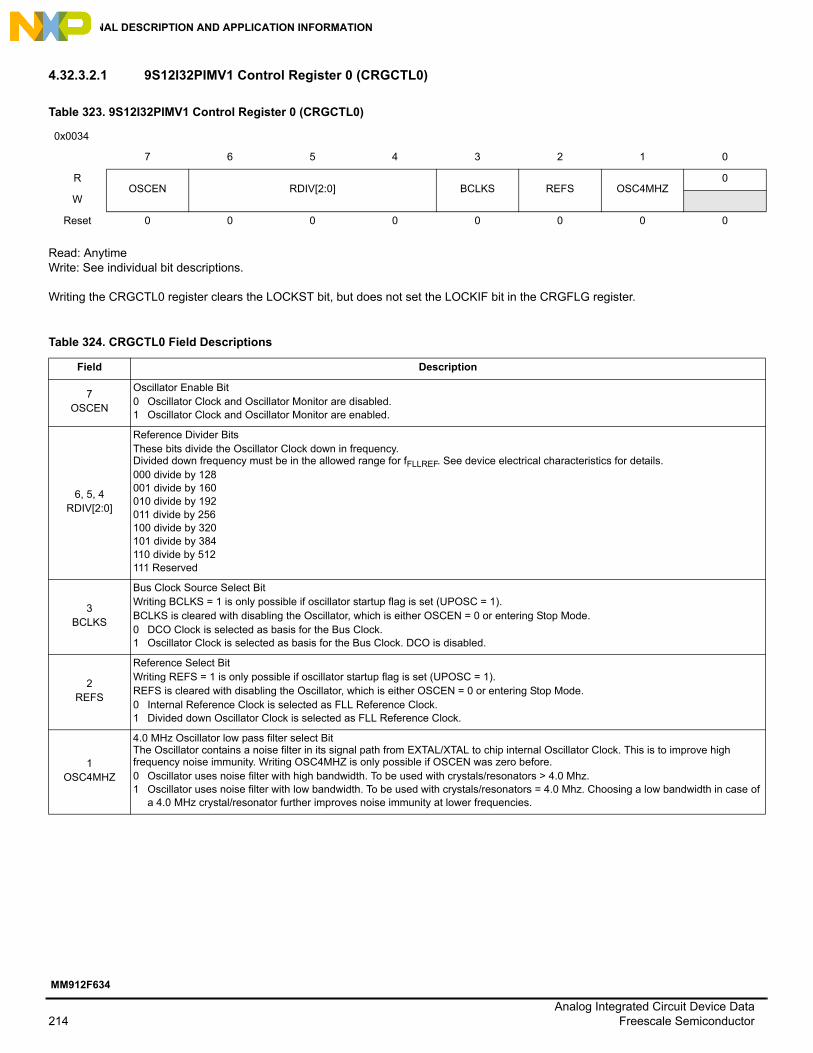
PTB1
373839404142434445464748
LS
1
BK
GD
NC
PG
ND
LS
2
ISE
NS
EL
ISE
NS
EH
NC
TE
ST
_A
TC
LK
RE
SE
T
242322212019181716151413
LIN
EV
DD
EV
SS
HS
UP
HS
2
HS
1
VS
2
VS
1
VS
EN
SE
DG
ND
VD
DX
VD
D
Analog Integrated Circuit Device DataFreescale Semiconductor 5
MM912F634
PIN ASSIGNMENT
3 XTAL MCU Oscillator PinXTAL is one of the optional crystal/resonator driver and external clock pins. On reset, all the device clocks are derived from the Internal Reference Clock. See Section 4.33, “External Oscillator (S12SOSCFPV1)".
4 TEST MCU Test PinThis input only pin is reserved for test. This pin has a pull-down device. The TEST pin must be tied to EVSS in user mode.
5 PA5 MCU PA5 PinGeneral purpose port A input or output pin 5. See Section 4.27, “Port Integration Module (9S12I32PIMV1)".
6 PA4 MCU PA4 PinGeneral purpose port A input or output pin 4. See Section 4.27, “Port Integration Module (9S12I32PIMV1)".
7 PA3 MCU PA3 / SS PinGeneral purpose port A input or output pin 3, shared with the SS signal of the integrated SPI Interface. See Section 4.27, “Port Integration Module (9S12I32PIMV1)".
8 PA2 MCU PA2 / SCK PinGeneral purpose port A input or output pin 2, shared with the SCLK signal of the integrated SPI Interface. See Section 4.27, “Port Integration Module (9S12I32PIMV1)".
9 PA1 MCU PA1 / MOSI PinGeneral purpose port A input or output pin 1, shared with the MOSI signal of the integrated SPI Interface. See Section 4.27, “Port Integration Module (9S12I32PIMV1)".
10 PA0 MCU PA0 / MISO PinGeneral-purpose port A input or output pin 0, shared with the MISO signal of the integrated SPI Interface. See Section 4.27, “Port Integration Module (9S12I32PIMV1)".
11 EVSSX MCU 5.0 V Ground Pin Ground for the MCU 5.0 V power supply.
12 EVDDX MCU 5.0 V Supply Pin MCU 5.0 V - I/O buffer supply. See Section 4.26, “MM912F634 - MCU Die Overview".
13 EVSS MCU 2.5 V Ground Pin Ground for the MCU 2.5 V power supply.
14 EVDD MCU 2.5 V Supply PinMCU 2.5 V - MCU Core- and Flash power supply. See Section 4.26, “MM912F634 - MCU Die Overview".
15 VDDVoltage Regulator Output 2.5 V
+2.5 V main voltage regulator output pin. External capacitor (CVDD) needed. See Section 4.4, “Power Supply".
16 VDDXVoltage Regulator Output 5.0 V
+5.0 V main voltage regulator output pin. External capacitor (CVDDX) needed. See Section 4.4, “Power Supply".
17 DGND Digital Ground PinThis pin is the device digital ground connection for the 5.0 V and 2.5 V logic. DGND, LGND, and AGND are internally connected to PGND via a back to back diode.
18 VSENSE Voltage Sense Pin
Battery voltage sense input. This pin can be connected directly to the battery line for voltage measurements. The voltage present at this input is scaled down by an internal voltage divider, and can be routed to the internal ADC via the analog multiplexer.The pin is self-protected against reverse battery connections. An external resistor (RVSENSE) is needed for protection(4). See Section 4.22, “Supply Voltage Sense - VSENSE".
19 VS1 Power Supply Pin 1
This pin is the device power supply pin 1. VS1 is primarily supplying the VDDX Voltage regulator and the Hall Sensor Supply Regulator (HSUP). VS1 can be sensed via a voltage divider through the AD converter. Reverse battery protection diode is required. See Section 4.4, “Power Supply"
20 VS2 Power Supply Pin 2This pin is the device power supply pin 2. VS2 supplies the High-side Drivers (HSx). Reverse battery protection diode required. See Section 4.4, “Power Supply"
21 HS1 High-side Output 1This pin is the first High-side output. It is supplied through the VS2 pin. It is designed to drive small resistive loads with optional PWM. In cyclic sense mode, this output activates periodically during low power mode. See Section 4.11, “High-side Drivers - HS".
22 HS2 High-side Output 2This pin is the second High-side output. It is supplied through the VS2 pin. It is designed to drive small resistive loads with optional PWM. In cyclic sense mode, this output activates periodically during low power mode. See Section 4.11, “High-side Drivers - HS".
23 HSUP Hall Sensor Supply OutputThis pin is designed as an 18 V Regulator to drive Hall Sensor Elements. It is supplied through the VS1 pin. An external capacitor (CHSUP) is needed. See Section 4.10, “Hall Sensor Supply Output - HSUP".
24 LIN LIN Bus I/OThis pin represents the single-wire bus transmitter and receiver. See Section 4.14, “LIN Physical Layer Interface - LIN".
25 LGND LIN Ground PinThis pin is the device LIN Ground connection. DGND, LGND, and AGND are internally connected to PGND via a back to back diode.
Table 3. MM912F634 Pin Description (continued)
Pin # Pin Name Formal Name Description
Analog Integrated Circuit Device Data6 Freescale Semiconductor
MM912F634
PIN ASSIGNMENT
26 PTB0 General Purpose I/O 0
This is the General Purpose I/O pin 0 based on VDDX with the following shared functions: • PTB0 - Bidirectional 5.0 V (VDDX) digital port I/O with selectable internal pull-up resistor. • AD0 - Analog Input Channel 0, 0…2.5 V (ADC2p5) analog input • TIM0CH0 - Timer Channel 0 Input/Output • Rx - Selectable connection to LIN / SCISee Section 4.17, “General Purpose I/O - PTB[0…2]".
27 PTB1 General Purpose I/O 1
This is the General Purpose I/O pin 1 based on VDDX with the following shared functions: • PTB1 - Bidirectional 5.0 V (VDDX) digital port I/O with selectable internal pull-up resistor. • AD1 - Analog Input Channel 1, 0…2.5 V (ADC2p5) analog input • TIM0CH1 - Timer Channel 1 Input/Output • Tx - Selectable connection to LIN / SCISee Section 4.17, “General Purpose I/O - PTB[0…2]".
28 PTB2 General Purpose I/O 2
This is the General Purpose I/O pin 2 based on VDDX with the following shared functions: • PTB2 - Bidirectional 5.0 V (VDDX) digital port I/O with selectable internal pull-up resistor. • AD2 - Analog Input Channel 2, 0…2.5 V (ADC2p5) analog input • TIM0CH2 - Timer Channel 2 Input/Output • PWM - Selectable connection to PWM Channel 0 or 1See Section 4.17, “General Purpose I/O - PTB[0…2]".
29 ADC2p5 ADC Reference VoltageThis pin represents the ADC reference voltage and has to be connected to a filter capacitor. See Section 4.19, “Analog Digital Converter - ADC"
30 AGND Analog Ground PinThis pin is the device Analog to Digital Converter ground connection. DGND, LGND and AGND are internally connected to PGND via a back to back diode.
31 L0 High Voltage Input 0
This pins is the High Voltage Input 0 with the following shared functions: • L0 - Digital High Voltage Input 0. When used as digital input, a series resistor (RLx) must
be used to protect against automotive transients.(5)
• AD3 - Analog Input 3 with selectable divider for 0…5.0 V and 0…18 V measurement range. • WU0 - Selectable Wake-up input 0 for wake up and cyclic sense during low power mode. See Section 4.16, “High Voltage Inputs - Lx"
32 L1 High Voltage Input 1
This pins is the High Voltage Input 1 with the following shared functions: • L1 - Digital High Voltage Input 1. When used as digital input, a series resistor (RLx) must
be used to protect against automotive transients.(5)
• AD4 - Analog Input 4 with selectable divider for 0…5.0 V and 0…18 V measurement range. • WU1 - Selectable Wake-up input 1 for wake-up and cyclic sense during low power mode.See Section 4.16, “High Voltage Inputs - Lx".
33 L2 High Voltage Input 2
This pins is the High Voltage Input 2 with the following shared functions: • L2 - Digital High Voltage Input 2. When used as digital input, a series resistor (RLx) must
be used to protect against automotive transients.(5)
• AD5 - Analog Input 5 with selectable divider for 0…5.0 V and 0…18 V measurement range. • WU2 - Selectable Wake-up input 2 for wake-up and cyclic sense during low power mode.See Section 4.16, “High Voltage Inputs - Lx".
34 L3 High Voltage Input 3
This pins is the High Voltage Input 3 with the following shared functions: • L3 - Digital High Voltage Input 3. When used as digital input, a series resistor (RLx) must
be used to protect against automotive transients.(5)
• AD6 - Analog Input 6 with selectable divider for 0…5.0 V and 0…18 V measurement range. • WU3 - Selectable Wake-up input 3 for wake-up and cyclic sense during low power mode.See Section 4.16, “High Voltage Inputs - Lx".
35 L4 High Voltage Input 4
This pins is the High Voltage Input 4 with the following shared functions: • L4 - Digital High Voltage Input 4. When used as digital input, a series resistor (RLx) must
be used to protect against automotive transients.(5)
• AD7 - Analog Input 7 with selectable divider for 0…5.0 V and 0…18 V measurement range. • WU4 - Selectable Wake-up input 4 for wake-up and cyclic sense during low power mode.See Section 4.16, “High Voltage Inputs - Lx". Note: This pin function is not available on all device configurations.
Table 3. MM912F634 Pin Description (continued)
Pin # Pin Name Formal Name Description
Analog Integrated Circuit Device DataFreescale Semiconductor 7
MM912F634
PIN ASSIGNMENT
2.2 MCU Die Signal Properties
This section describes the external MCU signals. It includes a table of signal properties.
36 L5 High Voltage Input 5
This pins is the High Voltage Input 5 with the following shared functions: • L5 - Digital High Voltage Input 5. When used as digital input, a series resistor (RLx) must
be used to protect against automotive transients.(5)
• AD8 - Analog Input 8 with selectable divider for 0…5.0 V and 0…18 V measurement range. • WU5 - Selectable Wake-up input 5 for wake-up and cyclic sense during low power mode.See Section 4.16, “High Voltage Inputs - Lx". Note: This pin function is not available on all device configurations.
37 LS1 Low-side Output 1Low-side output 1 used to drive small inductive loads like relays. The output is short-circuit protected, includes active clamp circuitry and can be also controlled by the PWM module.See Section 4.12, “Low-side Drivers - LSx".
38 PGND Power Ground PinThis pin is the device Low-side Ground connection. DGND, LGND and AGND are internally connected to PGND via a back to back diode.
39 LS2 Low-side Output 2Low-side output 2 used to drive small inductive loads like relays. The output is short-circuit protected, includes active clamp circuitry and can be also controlled by the PWM module.See Section 4.12, “Low-side Drivers - LSx".
40 ISENSEL Current Sense Pins LCurrent Sense differential input “Low”. This pin is used in combination with ISENSEH to measure the voltage drop across a shunt resistor. See Section 4.20, “Current Sense Module - ISENSE". Note: This pin function is not available on all device configurations.
41 ISENSEH Current Sense Pins HCurrent Sense differential input “High”. This pin is used in combination with ISENSEL to measure the voltage drop across a shunt resistor. Section 4.20, “Current Sense Module - ISENSE". Note: This pin function is not available on all device configurations.
42 NC Not connected Pin This pin is reserved for alternative function and should be left floating.
43 TEST_A Test Mode Pin Analog die Test Mode pin for Test Mode only. This pin must be grounded in user mode.
44 TCLK Test Clock InputTest Mode Clock Input pin for Test Mode only. The pin can be used to disable the internal watchdog for development purpose in user mode. See Section 4.9, “Window Watchdog". The pin is recommended to be grounded in user mode.
45 RESET_A Reset I/OBidirectional Reset I/O pin of the analog die. Active low signal. Internal pull-up. VDDX based. See Section 4.7, “Resets". To be externally connected to the RESET pin.
46 RESET MCU Reset PinThe RESET pin is an active low bidirectional control signal. It acts as an input to initialize the MCU to a known start-up state, and an output when an internal MCU function causes a reset. The RESET pin has an internal pull-up device to EVDDX.
47 BKGDMCU Background Debug and Mode Pin
The BKGD/MODC pin is used as a pseudo-open-drain pin for the background debug communication. It is used as MCU operating mode select pin during reset. The state of this pin is latched to the MODC bit at the rising edge of RESET. The BKGD pin has a pull-up device.
48 NC Not connected Pin This pin is reserved for alternative function and should be left floating or connected to GND.
Note:4. An optional filter capacitor CVSENSE is recommended to be placed between the board connector and RVSENSE to GND for increased ESD
performance.5. An optional filter capacitor CLx is recommended to be placed between the board connector and RLx to GND for increased ESD performance.
Table 4. Signal Properties Summary
Pin NameFunction 1
Pin NameFunction 2
PowerSupply
Internal Pull Resistor
DescriptionCTRL
Reset State
EXTAL — VDD NA NAOscillator pins
XTAL — VDD NA NA
RESET — VDDX Pull-up External reset
Table 3. MM912F634 Pin Description (continued)
Pin # Pin Name Formal Name Description
Analog Integrated Circuit Device Data8 Freescale Semiconductor
MM912F634
PIN ASSIGNMENT
TEST — N.A. RESET pin Down Test input
BKGD MODC VDDX Always on UP Background debug
PA5 — VDDX NA NA Port A I/O
PA4 — VDDX NA NA Port A I/O
PA3 SS VDDX NA NA Port A I/O, SPI
PA2 SCK VDDX NA NA Port A I/O, SPI
PA1 MOSI VDDX NA NA Port A I/O, SPI
PA0 MISO VDDX NA NA Port A I/O, SPI
Table 4. Signal Properties Summary (continued)
Pin NameFunction 1
Pin NameFunction 2
PowerSupply
Internal Pull Resistor
DescriptionCTRL
Reset State
Analog Integrated Circuit Device DataFreescale Semiconductor 9
MM912F634
ELECTRICAL CHARACTERISTICS
3 Electrical Characteristics
3.1 General
This supplement contains electrical information for the embedded MC9S12I32 microcontroller die, as well as the MM912F634 analog die.
3.2 Absolute Maximum Ratings
Absolute maximum ratings are stress ratings only. A functional operation under or outside those maxima is not guaranteed. Stress beyond those limits may affect the reliability or cause permanent damage of the device.
This device contains circuitry protecting against damage due to high static voltage or electrical fields. However, it is advised that normal precautions be taken to avoid application of any voltages higher than maximum-rated voltages to this high-impedance circuit. Reliability of operation is enhanced if unused inputs are tied to an appropriate voltage level. All voltages are with respect to ground unless otherwise noted.
Table 5. Absolute Maximum Electrical Ratings - Analog Die
Ratings Symbol Value Unit
Supply Voltage at VS1 and VS2Normal Operation (DC)Transient Conditions (load dump)Transient input voltage with external component (according to LIN Conformance Test Specification / ISO7637-2)
VSUP(SS)VSUP(PK)VSUP(TR)
-0.3 to 27-0.3 to 40
see Section 3.9, “Additional Test
Information ISO7637-2"
V
L0…L5 - Pin VoltageNormal Operation with a series RLX resistor (DC)Transient input voltage with external component (according to LIN Conformance Test Specification / ISO7637-2)
VLxDCVLxTR
-27 to 40see Section 3.9, “Additional Test
Information ISO7637-2"
V
LIN Pin VoltageNormal Operation (DC)Transient input voltage with external component (according to LIN Conformance Test Specification / ISO7637-2)
VBUSDCVBUSTR
-33 to 40see Section 3.9, “Additional Test
Information ISO7637-2"
V
Supply Voltage at VDDX VDDX -0.3 to 5.5 V
Supply Voltage at VDD (6) VDD -0.3 to 2.75 V
VDD output current IVDD Internally Limited A
VDDX output current IVDDX Internally Limited A
TCLK Pin Voltage VTCLK -0.3 to 10 V
RESET_A Pin Voltage VIN -0.3 to VDDx+0.3 V
Input / Output Pins PTB[0:2] Voltage VIN -0.3 to VDDx+0.3 V
HS1 and HS2 Pin Voltage (DC) VHS -0.3 to VS2+0.3 V
LS1 and LS2 Pin Voltage (DC) VLS -0.3 to 45 V
ISENSEH and ISENSEL Pin Voltage (DC) VISENSE -0.3 to 40 V
HSUP Pin Voltage (DC) VHSUP -0.3 to VS1+0.3 V
VSENSE Pin Voltage (DC) VVSENSE -27 to 40 V
Note:6. Caution: As this pin is adjacent to the VDDX pin, care should be taken to avoid a short between VDD and VDDX, for example, during the soldering
process. A short-circuit between these pins might lead to permanent damage.
Analog Integrated Circuit Device Data10 Freescale Semiconductor
MM912F634
ELECTRICAL CHARACTERISTICS
3.3 Operating Conditions
This section describes the operating conditions of the device. Unless otherwise noted those conditions apply to all the following data.
Table 6. Maximum Electrical Ratings - MCU Die
Ratings Symbol Value Unit
5.0 V Supply Voltage VEDDX -0.3 to 6.0 V
2.5 V Supply Voltage VEDD -0.3 to 2.75 V
Digital I/O input voltage (PA0...PA7, PE0, PE1) VIN -0.3 to 6.0 V
EXTAL, XTAL VILV -0.3 to 2.16 V
TEST input VTEST -0.3 to 10.0 V
Instantaneous maximum currentSingle pin limit for all digital I/O pins
ID
-25 to 25 mA
Instantaneous maximum currentSingle pin limit for EXTAL, XTAL
Two layer board (JEDEC 1s)Junction to Ambient Natural Convection (7), (8)
RJARJB
RJA
5931
96
C/W
Peak Package Reflow Temperature During Reflow (10),(11) TPPRT 300 °C
Notes7. Junction temperature is a function of die size, on-chip power dissipation, package thermal resistance, mounting site (board) temperature, ambient
temperature, air flow, power dissipation of other components on the board, and board thermal resistance.8. Per JEDEC JESD51-6 with the board (JESD51-7) horizontal.9. Thermal resistance between the die and the printed circuit board per JEDEC JESD51-8. Board temperature is measured on the top surface of the
board near the package.10. Pin soldering temperature limit is for 10 seconds maximum duration. Not designed for immersion soldering. Exceeding these limits may cause
malfunction or permanent damage to the device.11. Freescale’s Package Reflow capability meets Pb-free requirements for JEDEC standard J-STD-020C. For Peak Package Reflow Temperature and
Moisture Sensitivity Levels (MSL), Go to www.freescale.com, search by part number [e.g. remove prefixes/suffixes and enter the core ID to view all orderable parts. (i.e. MC34xxxD enter 34xxx), and review parametrics.
Table 8. Operating Conditions
Ratings Symbol Value Unit
Analog Die Nominal Operating Voltage VSUP 5.5 to 18 V
Analog Die Functional Operating Voltage - Device is fully functional. All features are operating.
VSUPOP 5.5 to 27 V
MCU I/O and supply voltage(12) VEDDX 4.5 to 5.5 V
Analog Integrated Circuit Device DataFreescale Semiconductor 11
This section describes the current consumption characteristics of the device as well as the conditions for the measurements.
3.4.1 Measurement Conditions
All measurements are without output loads. Unless otherwise noted, the currents are measured in MCU special single chip mode and the CPU code is executed from RAM.
MCU Digital logic supply voltage(12) VEDD 2.25 to 2.75 V
MCU External Oscillator fOSC 4.0 to 16 MHz
MCU Bus frequency fBUS fBUSMAX(13) MHz
Operating Ambient Temperature, MM912x634xVxxx TA -40 to 105 C
Operating Junction Temperature - Analog Die TJ_A -40 to 150 C
Operating Junction Temperature - MCU Die TJ_M -40 to 140 C
Note:12. During power up and power down sequence always VDD < VDDX13. fBUSMAX frequency ratings differ by device and is specified in Table 1
Table 9. Supply Currents
Ratings Symbol Min Typ(14) Max Unit
Normal Mode analog die only, excluding external loads, LIN Recessive State (5.5 V VSUP 18 V, 2.25 V EVDD 2.75 V, 4.5 V EVDDX 5.5 V, -40 °C TJ_A 150 °C).
IRUN_A - 5.0 8.0 mA
Normal Mode MCU die only (TJ_M = 140 °C; VDD = 2.75 V, VDDX = 5.5 V, fOSC = 4.0 MHz, fBUS = fBUSMAX
(18))(15)IRUN_M - 12.5 15 mA
Stop Mode internal analog die only, excluding external loads, LIN Recessive State, Lx enabled, measured at VS1+VS2 (5.5 V VSUP 18 V, 2.25 V EVDD 2.75 V, 4.5 V EVDDX 5.5 V)-40 °C TJ_A 125 °C125 °C TJ_A 140 °C
ISTOP_A
--
20-
4050
µA
Stop Mode MCU die only (VDD = 2.75 V, VDDX = 5.5 V, fOSC = 4.0 MHz, fBUS = fBUSMAX
(18); MCU in STOP; RTI and COP off)(16)
TJ_M = 140 °CTJ_M = 105 °CTJ_M = 25 °C
ISTOP_M
---
0.1350.0350.010
0.4000.2000.030
mA
Stop Mode MCU die only (VDD = 2.75 V, VDDX = 5.5 V, fOSC = 4.0 MHz, fBUS = fBUSMAX
(18); All modules except RTI disabled)(17)IWAIT_M - 7.0 12 mA
Sleep Mode (VDD = VDDX = OFF; 5.5 V VSUP 18 V; -40 °C TJ_A 150 °C; 3.0 V LX 1.0 V).
ISLEEP - 15 28 µA
Cyclic Sense Supply Current Adder (5.0 ms Cycle) ICS - 15 20 µA
Note:14. Typical values noted reflect the approximate parameter mean at TA = 25 °C15. IRUN_M denotes the sum of the currents flowing into VDD and VDDX.16. ISTOP_M denotes the sum of the currents flowing into VDD and VDDX.17. IWAIT_M denotes the sum of the currents flowing into VDD and VDDX.18. fBUSMAX frequency ratings differ by device and is specified in Table 1.
Table 8. Operating Conditions (continued)
Ratings Symbol Value Unit
Analog Integrated Circuit Device Data12 Freescale Semiconductor
MM912F634
ELECTRICAL CHARACTERISTICS
3.5 Static Electrical CharacteristicsStatic electrical characteristics noted under conditions 5.5V VSUP 18 V, -40 °C TA 105 °C, unless otherwise noted. Typical values noted reflect the approximate parameter mean at TA = 25 °C under nominal conditions unless otherwise noted.
3.5.1 Static Electrical Characteristics Analog Die
Table 10. Static Electrical Characteristics - Power Supply
Ratings Symbol Min Typ Max Unit
Power-On Reset (POR) Threshold (measured on VS1) VPOR 1.5 - 3.5 V
Low Voltage Warning (LVI) Threshold (measured on VS1, falling edge)Hysteresis (measured on VS1)
VLVIVLVI_H
5.55-
6.01.0
6.6-
V
High Voltage Warning (HVI) Threshold (measured on VS2, rising edge)Hysteresis (measured on VS2)
VHVIVHVI_H
18-
19.251.0
20.5-
V
Low Battery Warning (LBI) Threshold (measured on VSENSE, falling edge)Hysteresis (measured on VSENSE)
VLBIVLBI_H
5.55-
6.01.0
6.6-
V
J2602 Undervoltage threshold VJ2602UV 5.5 5.7 6.2 V
Low VDDX Voltage (LVRX) Threshold VLVRX 2.7 3.0 3.3 V
Low VDD Voltage Reset (LVR) Threshold Normal Mode VLVR 2.30 2.35 2.4 V
Low VDD Voltage Reset (LVR) Threshold Stop Mode (19) VLVRS 1.6 1.85 2.1 V
VDD Overvoltage Threshold (VROV) VVDDOV 2.575 2.7875 3.0 V
VDDX Overvoltage Threshold (VROVX) VVDDXOV 5.25 5.675 6.1 V
Note:19. See MM912F634ER, MM912F634, Silicon Analog Mask (M91W) / Digital Mask (M33G) Errata
Voltage Drop at the serial Diode DSER_INT 0.4 0.7 1.0 V
LIN Pull-up Resistor RSLAVE 20 30 60 k
Bus Wake-up Threshold from Stop or Sleep(22) VWUP 4.5 5.0 6.0 V
Bus Dominant Voltage VDOM - - 2.5 V
Note:22. Considering drop from VBAT to LIN, at very low VBAT level, the internal logic detects a dominant as the threshold does not decrease with VSUP.
Table 19. Static Electrical Characteristics - High Voltage Inputs - Lx
Ratings Symbol Min Typ Max Unit
Low Detection Threshold 7.0 V VSUP 27 V5.5 V VSUP 7 V
VTHL 2.21.5
2.52.5
3.44.0
V
High Detection Threshold7.0 V VSUP 27 V5.5 V VSUP 7 V
VTHH 2.62.0
3.03.0
3.74.5
V
Hysteresis5.5 V VSUP 27 V
VHYS 0.25 0.45 1.0 V
Input Current Lx (-0.2 V < VIN < VS1) IIN -10 - 10 µA
Analog Input Impedance Lx RLxIN - - 1.2 M
Lx Series Resistor RLx 9.5 10 10.5 k
Lx Capacitor (optional)(23) CLx - 100 - nF
Analog Input Divider Ratio (RATIOLx = VLx / VADOUT0)LXDS (Lx Divider Select) = 0LXDS (Lx Divider Select) = 1
RATIOLx --
2.07.2
--
Analog Input Divider Ratio Accuracy RATIOLX -5.5 - 5.5 %
Analog Inputs Channel Ratio - MismatchLXDS (Lx Divider Select) = 0LXDS (Lx Divider Select) = 1
LxMATCH --
--
5.05.0
%
Note:23. The ESD behavior specified in Section 3.8, “ESD Protection and Latch-up Immunity" are guaranteed without the optional capacitor.
Total Error with offset compensation TE -5.0 - 5.0 LSB
Bandgap measurement Channel (CH14) Valid Result Range (including 7.0% bg1p25 sleep accuracy + high-impedance measurement error of 5.0% at fADC)(25) ADCH14 1.1 1.25 1.4 V
Note:24. No external load allowed on the ADC2p5 pin.25. Reduced ADC frequency lowers measurement error.
Analog Integrated Circuit Device DataFreescale Semiconductor 17
MM912F634
ELECTRICAL CHARACTERISTICS
Table 22. Static Electrical Characteristics - Current Sense Module - ISENSE
Ratings Symbol Min Typ Max Unit
GainCSGS (Current Sense Gain Select) = 000CSGS (Current Sense Gain Select) = 001CSGS (Current Sense Gain Select) = 010CSGS (Current Sense Gain Select) = 011CSGS (Current Sense Gain Select) = 100CSGS (Current Sense Gain Select) = 101CSGS (Current Sense Gain Select) = 110CSGS (Current Sense Gain Select) = 111
G
--------
7.09.0101214182436
--------
Gain Accuracy -3.0 - 3.0 %
Offset -1.5 - 1.5 %
Resolution(26) RES - 51 - mA/LSB
ISENSEH, ISENSEL Input Common Mode Voltage Range VIN -0.2 - 3.0 V
Current Sense Module - Normal Mode Current Consumption Adder (CSE = 1) IISENSE - 600 - µA
Note:26. RES = 2.44 mV/(GAIN*RSHUNT)
Table 23. Static Electrical Characteristics - Temperature Sensor - TSENSE
Ratings Symbol Min Typ Max Unit
Internal Chip Temperature Sense Gain(27) TSG - 9.17 - mV/k
Internal Chip Temperature Sense Error at the end of conversion(27) TSERR –5.0 - 5.0 °C
Temperature represented by a ADCIN Voltage of 0.150 V(27) T0.15V -55 -50 -45 °C
Temperature represented by a ADCIN Voltage of 1.984 V(27) T1.984V 145 150 155 °C
Note:27. Guaranteed by design and characterization.
Table 24. Static Electrical Characteristics - Supply Voltage Sense - VSENSE and VS1SENSE
Ratings Symbol Min Typ Max Unit
VSENSE Input Divider Ratio (RATIOVSENSE = VVSENSE / ADCIN)5.5 V < VSUP < 27 V
RATIOVSENSE 10.8
VSENSE error - whole path (VSENSE pin to Digital value) ERVSENSE - - 5.0 %
VS1SENSE Input Divider Ratio (RATIOVS1SENSE = VVS1SENSE / ADCIN)5.5 V < VSUP < 27 V
RATIOVS1SENSE 10.8
VS1SENSE error - whole path (VS1 pin to Digital value) ERVS1SENSE - - 5.0 %
Note:28. The ESD behavior specified in Section 3.8, “ESD Protection and Latch-up Immunity" is guaranteed without the optional capacitor.
Analog Integrated Circuit Device Data18 Freescale Semiconductor
MM912F634
ELECTRICAL CHARACTERISTICS
3.5.2 Static Electrical Characteristics MCU Die
3.5.2.1 I/O Characteristics
This section describes the characteristics of all I/O pins except EXTAL, XTAL, TEST and supply pins.
3.6 Dynamic Electrical CharacteristicsDynamic electrical characteristics noted under conditions 5.5V VSUP 18 V, -40 °C TA 105 °C, unless otherwise noted. Typical values noted reflect the approximate parameter mean at TA = 25 °C under nominal conditions unless otherwise noted.
3.6.1 Dynamic Electrical Characteristics Analog Die
Table 25. 5.0 V I/O Characteristics for PTA, RESET and BKGD Pins
Ratings Symbol Min Typ Max Unit
Input high voltage VIH
0.65*VDD - - V
Input high voltage VIH - - VDD + 0.3 V
Input low voltage VIL - - 0.35*VDD V
Input low voltage VIL VSS - 0.3 - - V
Input hysteresis VHYS - 250 - mV
Input leakage current (pins in high-impedance input mode)Vin = VDDX or VSSX
IIN
-1.0 - 1.0 A
Output high voltage (pins in output mode) Partial Drive IOH = -2.0 mA VOH
VDD – 0.8 - - V
Output high voltage (pins in output mode) Full Drive IOH = -10 mA VOH
VDD – 0.8 - - V
Output low voltage (pins in output mode) Partial drive IOL = +2.0 mA VOL - - 0.8 V
Output low voltage (pins in output mode) Full Drive IOL = +10 mA VOL - - 0.8 V
Internal pull-up resistance (VIHmin > input voltage > VILmax) RPUL 25 - 50 k
Internal pull-down resistance (VIHmin > input voltage > VILmax) RPDH 25 - 50 k
Input capacitance Cin - 6.0 - pF
Injection current(29)
Single pin limitTotal device Limit, sum of all injected currents
IICSIICP
-2.5-25
--
2.525
mA
Note:29. Refer to Section 3.8, “ESD Protection and Latch-up Immunity" for more details.
Table 26. Dynamic Electrical Characteristics - Modes of Operation
Ratings Symbol Min Typ Max Unit
VDD Short Timeout tVTO 110 150 205 ms
Analog Base Clock fBASE - 100 - kHz
Reset Delay tRST 140 200 280 µs
Table 27. Dynamic Electrical Characteristics - Power Supply
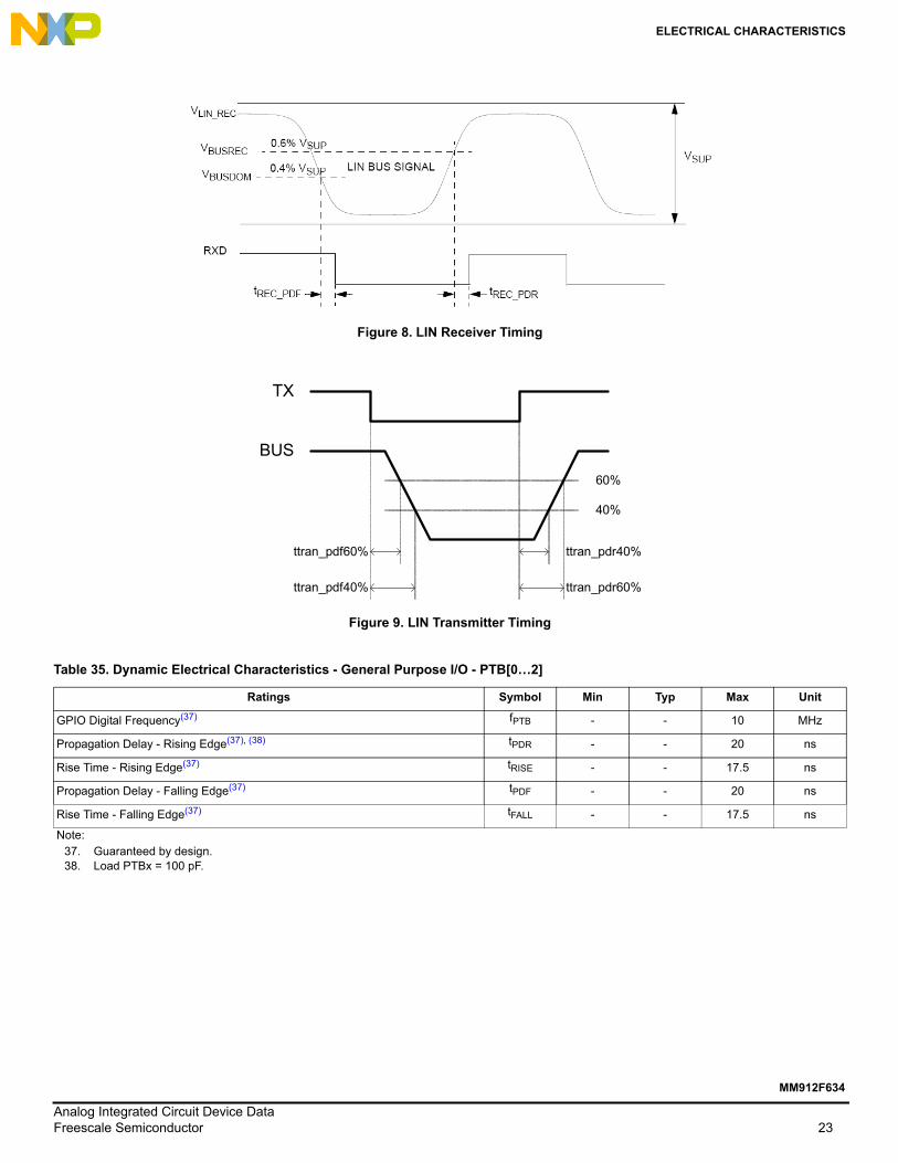
LIN Driver - 20.0 kBit/s; Bus load conditions (CBUS; RBUS): 1.0 nF; 1.0 k / 6,8 nF;660 / 10 nF;500 . Measurement thresholds: 50% of TXD signal to LIN signal threshold defined at each parameter. See Figure 5 and Figure 6.
Duty Cycle 1:THREC(MAX) = 0.744 x VSUP, THDOM(MAX) = 0.581 x VSUP, 7.0 V VSUP18 V; tBit = 50 µs;, D1 = tBUS_REC(MIN)/(2 x tBit)
D1 0.396 - -
Duty Cycle 2:THREC(MIN) = 0.422 x VSUP, THDOM(MIN) = 0.284 x VSUP, 7.6 V VSUP18 V; tBIT = 50 µs, D2 = tBUS_REC(MAX)/(2 x tBIT)
D2 - - 0.581
LIN Driver - 10.0 kBit/s; Bus load conditions (CBUS; RBUS): 1.0 nF; 1.0 k / 6,8 nF;660 / 10 nF;500 Measurement thresholds: 50% of TXD signal to LIN signal threshold defined at each parameter. See Figure 5 and Figure 7.
Duty Cycle 3:THREC(MAX) = 0.778 x VSUP, THDOM(MAX) = 0.616 x VSUP, 7.0 V VSUP18 V; tBIT = 96 µs, D3 = TBUS_REC(MIN)/(2 x tBIT)
D3 0.417 - -
Duty Cycle 4:THREC(MIN) = 0.389 x VSUP, THDOM(MIN) = 0.251 x VSUP, 7.6 V VSUP18 V; tBIT = 96 µs, D4 = tBUS_REC(MAX)/(2 x tBIT)
Note:37. Guaranteed by design.38. Load PTBx = 100 pF.
BUS
TX
60%
40%
ttran_pdr60%
ttran_pdr40%ttran_pdf60%
ttran_pdf40%
Analog Integrated Circuit Device DataFreescale Semiconductor 23
MM912F634
ELECTRICAL CHARACTERISTICS
3.6.2 Dynamic Electrical Characteristics MCU Die
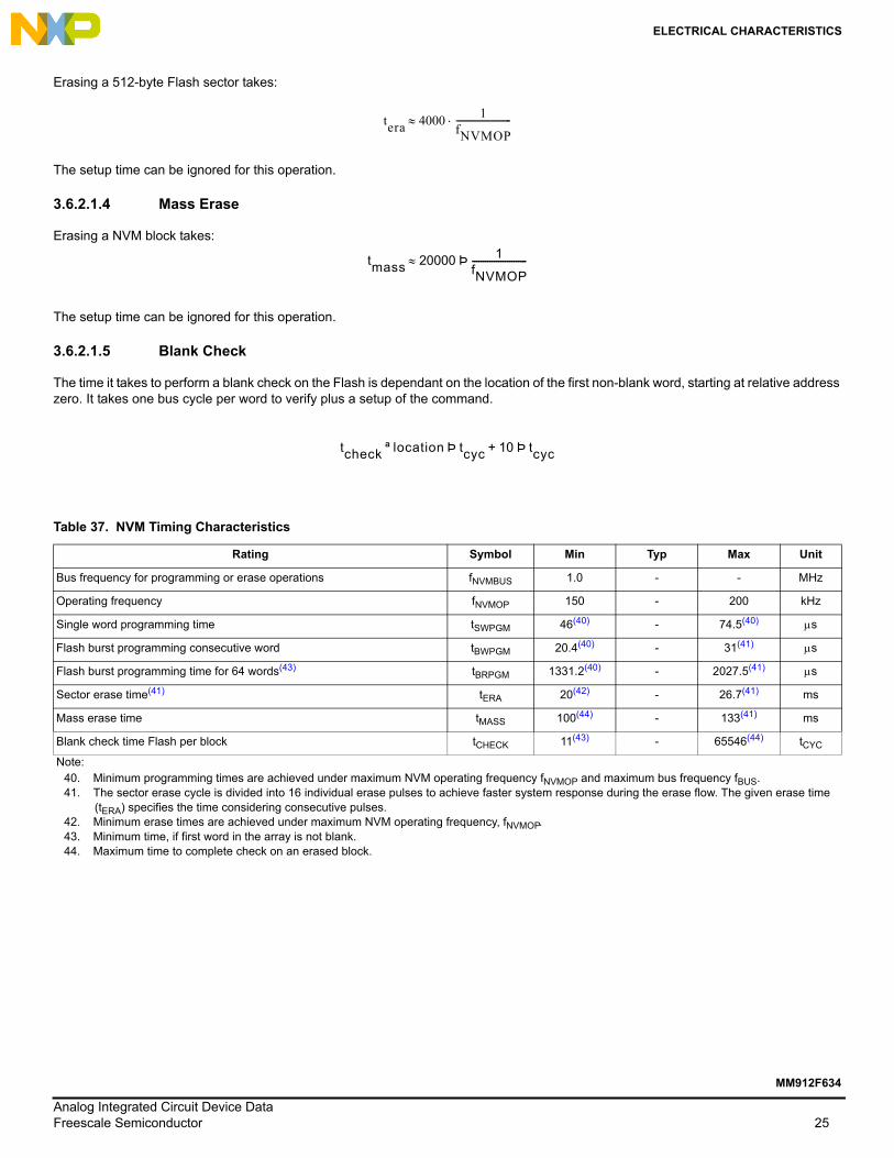
3.6.2.1 NVM Timing
The time base for all NVM program or erase operations is derived from the bus block. A minimum bus frequency fNVMBUS is required for performing program or erase operations. The NVM module do not has any means to monitor the frequency and does not prevent a program or erase operation at frequencies above or below the specified minimum. Attempting to program or erase the NVM modules at a lower frequency, a full program, or erase transition is not assured.
The Flash program and erase operations are timed using a clock derived from the bus clock using the FCLKDIV and register. The frequency of this clock must be set within the limits specified as fNVMOP.
The minimum program and erase times shown in Table 37 are calculated for maximum fNVMOP and maximum fBUS. The maximum times are calculated for minimum fNVMOP and a fBUS of 2.0 MHz.
3.6.2.1.1 Single Word Programming
The programming time for single word programming is dependant on the bus frequency as a well as on the frequency fNVMOP, and can be calculated according to the following formula.
3.6.2.1.2 Burst Programming
This applies only to the Flash, where up to 64 words in a row can be programmed consecutively, using burst programming by keeping the command pipeline filled. The time to program a consecutive word can be calculated as:
The time to program a whole row is:
Burst programming is more than 2 times faster than single word programming.
3.6.2.1.3 Sector Erase
NOTEThe sector erase cycle is divided into 16 individual erase pulses to achieve faster system response during the erase flow. The given erase time (tERA) specifies the time considering consecutive pulses.
Table 36. Dynamic Electrical Characteristics - Analog Digital Converter - ADC
Ratings Symbol Min Typ Max Unit
ADC Operating Frequency(39) fADC 1.6 2.0 2.4 MHz
Conversion Time (from ACCR write to CC Flag)(39) tCONV 26 clk
Sample Frequency Channel 14 (Bandgap)(39) fCH14 - - 2.5 kHz
Note:39. Guaranteed by design.
tswpgm 91
fNVMOP------------------------- 25
1fbus-----------+=
tbwpgm 41
fNVMOP------------------------- 9
1fbus-----------+=
tbrpgm tswpgm 63 tbwpgm+=
Analog Integrated Circuit Device Data24 Freescale Semiconductor
MM912F634
ELECTRICAL CHARACTERISTICS
Erasing a 512-byte Flash sector takes:
The setup time can be ignored for this operation.
3.6.2.1.4 Mass Erase
Erasing a NVM block takes:
The setup time can be ignored for this operation.
3.6.2.1.5 Blank Check
The time it takes to perform a blank check on the Flash is dependant on the location of the first non-blank word, starting at relative address zero. It takes one bus cycle per word to verify plus a setup of the command.
Table 37. NVM Timing Characteristics
Rating Symbol Min Typ Max Unit
Bus frequency for programming or erase operations fNVMBUS 1.0 - - MHz
Operating frequency fNVMOP 150 - 200 kHz
Single word programming time tSWPGM 46(40) - 74.5(40) s
Flash burst programming consecutive word tBWPGM 20.4(40) - 31(41) s
Flash burst programming time for 64 words(43) tBRPGM 1331.2(40) - 2027.5(41) s
Sector erase time(41) tERA 20(42) - 26.7(41) ms
Mass erase time tMASS 100(44) - 133(41) ms
Blank check time Flash per block tCHECK 11(43) - 65546(44) tCYC
Note:40. Minimum programming times are achieved under maximum NVM operating frequency fNVMOP and maximum bus frequency fBUS. 41. The sector erase cycle is divided into 16 individual erase pulses to achieve faster system response during the erase flow. The given erase time
(tERA) specifies the time considering consecutive pulses.42. Minimum erase times are achieved under maximum NVM operating frequency, fNVMOP.43. Minimum time, if first word in the array is not blank.44. Maximum time to complete check on an erased block.
tera 40001
fNVMOP-------------------------
tmass 20000 1fNVMOP-------------------------Þ
tcheck location tcyc 10 tcycÞ+Þª
Analog Integrated Circuit Device DataFreescale Semiconductor 25
MM912F634
ELECTRICAL CHARACTERISTICS
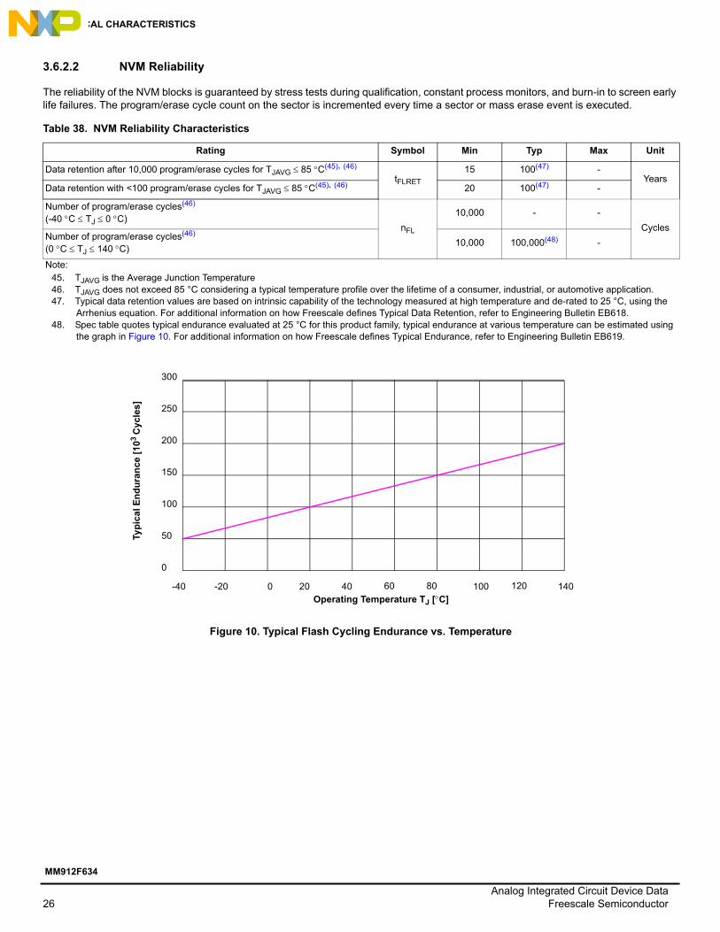
3.6.2.2 NVM Reliability
The reliability of the NVM blocks is guaranteed by stress tests during qualification, constant process monitors, and burn-in to screen early life failures. The program/erase cycle count on the sector is incremented every time a sector or mass erase event is executed.
Figure 10. Typical Flash Cycling Endurance vs. Temperature
Table 38. NVM Reliability Characteristics
Rating Symbol Min Typ Max Unit
Data retention after 10,000 program/erase cycles for TJAVG 85 C(45), (46)
tFLRET
15 100(47) -Years
Data retention with <100 program/erase cycles for TJAVG 85 C(45), (46) 20 100(47) -
Number of program/erase cycles(46)
(-40 C TJ 0 C)nFL
10,000 - -
CyclesNumber of program/erase cycles(46)
(0 C TJ 140 C)10,000 100,000(48) -
Note:45. TJAVG is the Average Junction Temperature46. TJAVG does not exceed 85 °C considering a typical temperature profile over the lifetime of a consumer, industrial, or automotive application.47. Typical data retention values are based on intrinsic capability of the technology measured at high temperature and de-rated to 25 °C, using the
Arrhenius equation. For additional information on how Freescale defines Typical Data Retention, refer to Engineering Bulletin EB618.48. Spec table quotes typical endurance evaluated at 25 °C for this product family, typical endurance at various temperature can be estimated using
the graph in Figure 10. For additional information on how Freescale defines Typical Endurance, refer to Engineering Bulletin EB619.
Typ
ical
En
du
ran
ce [
103
Cyc
les]
Operating Temperature TJ [C]
0
50
100
150
200
250
300
-40 -20 0 20 40 60 80 100 120 140
Analog Integrated Circuit Device Data26 Freescale Semiconductor
MM912F634
ELECTRICAL CHARACTERISTICS
3.6.2.3 Reset, Oscillator and Internal Clock Generation
3.6.2.3.1 Startup & FLL Characteristics
Table 39 summarizes several startup characteristics explained in this section. Detailed description of the startup behavior can be found in the Clock and Reset Generator (CRG) block description.
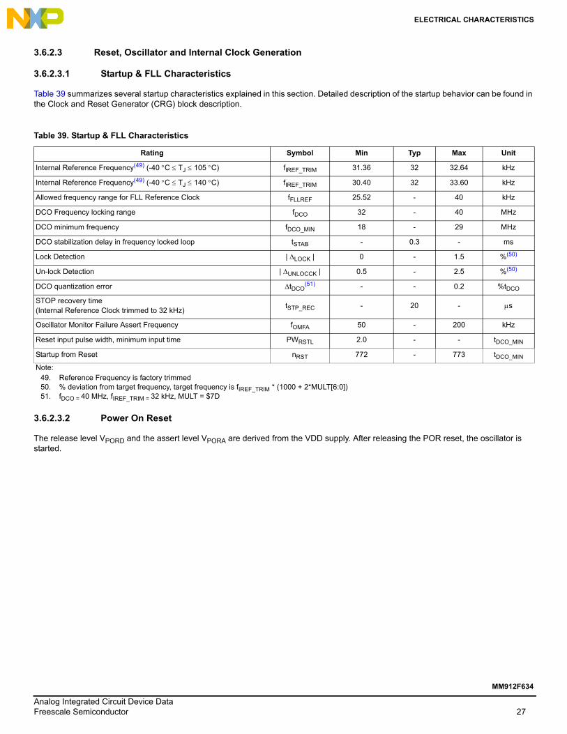
3.6.2.3.2 Power On Reset
The release level VPORD and the assert level VPORA are derived from the VDD supply. After releasing the POR reset, the oscillator is started.
Table 39. Startup & FLL Characteristics
Rating Symbol Min Typ Max Unit
Internal Reference Frequency(49) (-40 C TJ 105 C) fIREF_TRIM 31.36 32 32.64 kHz
Internal Reference Frequency(49) (-40 C TJ 140 C) fIREF_TRIM 30.40 32 33.60 kHz
Allowed frequency range for FLL Reference Clock fFLLREF 25.52 - 40 kHz
DCO Frequency locking range fDCO 32 - 40 MHz
DCO minimum frequency fDCO_MIN 18 - 29 MHz
DCO stabilization delay in frequency locked loop tSTAB - 0.3 - ms
Lock Detection | LOCK | 0 - 1.5 %(50)
Un-lock Detection | UNLOCCK | 0.5 - 2.5 %(50)
DCO quantization error tDCO(51) - - 0.2 %tDCO
STOP recovery time(Internal Reference Clock trimmed to 32 kHz)
tSTP_REC - 20 - s
Oscillator Monitor Failure Assert Frequency fOMFA 50 - 200 kHz
Note:49. Reference Frequency is factory trimmed50. % deviation from target frequency, target frequency is fIREF_TRIM * (1000 + 2*MULT[6:0])51. fDCO = 40 MHz, fIREF_TRIM = 32 kHz, MULT = $7D
Analog Integrated Circuit Device DataFreescale Semiconductor 27
MM912F634
ELECTRICAL CHARACTERISTICS
Figure 11. Power on Reset
3.6.2.3.3 Oscillator
The device features an internal full-swing Pierce oscillator configuration. The device features an oscillator monitor. An oscillator monitor failure is asserted if the frequency is below the assert frequency fCMFA.
3.6.2.4 SPI Timing
This section provides electrical parameters and ratings for the SPI. Table 42 lists the measurement conditions.
Table 40. Power On Reset Characteristics
Rating Symbol Min Typ Max Unit
Power On Reset assert level VPORA 0.84 1.51 - V
Power On Reset de-assert level VPORD - 1.51 2.01 V
Table 41. Oscillator Characteristics
Rating Symbol Min Typ Max Unit
Crystal oscillator range fOSC 4.0 - 16 MHz
Oscillator start-up time(52) tUPOSC - 2.0 5.0 ms
Clock Monitor Failure Assert Frequency fCMFA 50 100 200 KHz
Thresholds for delay measurement points (20% / 80%) VDDX V
Note:53. Timing specified for equal load on all SPI output pins. Avoid asymmetric load.
VPORD
POR
t
V VDD
VPORA
Analog Integrated Circuit Device Data28 Freescale Semiconductor
MM912F634
ELECTRICAL CHARACTERISTICS
3.6.2.4.1 Master Mode
Figure 12 depicts the timing diagram for master mode with transmission format CPHA = 0.
Figure 12. SPI Master Timing (CPHA = 0)
In Figure 13 depicts the timing diagram for master mode with transmission format CPHA=1.
Figure 13. SPI Master Timing (CPHA = 1)
Table 43 lists the timing characteristics for master mode.
SCK
(Output)
SCK
(Output)
MISO(Input)
MOSI(Output)
SS1(Output)
1
9
5 6
MSB IN2
Bit MSB-1…1
LSB IN
MSB OUT2 LSB OUT
Bit MSB-1… 1
11
4
4
2
10
(CPOL = 0)
(CPOL = 1)
313
13
1. If configured as an output.2. LSBF = 0. For LSBF = 1, bit order is LSB, bit 1, bit 2... MSB.
12
12
SCK
(Output)
SCK
(Output)
MISO(Input)
MOSI(Output)
1
5 6
MSB IN2
Bit MSB-1… 1
LSB IN
Master MSB OUT2 Master LSB OUT
Bit MSB-1… 1
44
9
12 13
11
Port Data
(CPOL = 0)
(CPOL = 1)
Port Data
SS1(Output)
2 12 13 3
1.If configured as output2. LSBF = 0. For LSBF = 1, bit order is LSB, bit 1,bit 2... MSB.
Analog Integrated Circuit Device DataFreescale Semiconductor 29
MM912F634
ELECTRICAL CHARACTERISTICS
3.6.2.4.2 Slave Mode
Figure 14 depicts the timing diagram for slave mode with transmission format CPHA = 0.
Figure 14. SPI Slave Timing (CPHA = 0)
Table 43. SPI Master Mode Timing Characteristics
Characteristic Symbol Min Typ Max Unit
SCK frequency fSCK 1/2048 - 12 fBUS
SCK period tSCK 2.0 - 2048 tBUS
Enable lead time tLEAD - 1/2 - tSCK
Enable lag time tLAG - 1/2 - tSCK
Clock (SCK) high or low time tWSCK - 1/2 - tSCK
Data setup time (inputs) tSU 8.0 - - ns
Data hold time (inputs) tHI 8.0 - - ns
Data valid after SCK edge tVSCK - - 29 ns
Data valid after SS fall (CPHA = 0) tVSS - - 15 ns
Data hold time (outputs) tHO 20 - - ns
Rise and fall time inputs tRFI - - 8.0 ns
Rise and fall time outputs tRFO - - 8.0 ns
SCK
(Input)
SCK
(Input)
MOSI(Input)
MISO(Output)
SS(Input)
1
9
5 6
MSB IN
Bit MSB-1…1
LSB IN
Slave MSB Slave LSB OUT
Bit MSB-1…1
11
442
7
(CPOL = 0)
(CPOL = 1)
3
13
NOTE: Not defined
12
12
11
See
13
Note
810
See Note
Analog Integrated Circuit Device Data30 Freescale Semiconductor
MM912F634
ELECTRICAL CHARACTERISTICS
Figure 15 depicts the timing diagram for slave mode with transmission format CPHA = 1.
Figure 15. SPI Slave Timing (CPHA = 1)
Table 44 lists the timing characteristics for slave mode.
Table 44. SPI Slave Mode Timing Characteristics
Characteristic Symbol Min Typ Max Unit
SCK frequency fSCK DC - 14 fBUS
SCK period tSCK 4.0 - tBUS
Enable lead time tLEAD 4.0 - - tBUS
Enable lag time tLAG 4.0 - - tBUS
Clock (SCK) high or low time tWSCK 4.0 - - tBUS
Data setup time (inputs) tSU 8.0 - - ns
Data hold time (inputs) tHI 8.0 - - ns
Slave access time (time to data active) tA - - 20 ns
Slave MISO disable time tDIS - - 22 ns
Data valid after SCK edge tVSCK - - 29 + 0.5 tBUS(53) ns
Data valid after SS fall tVSS - - 29 + 0.5 tBUS(53) ns
Data hold time (outputs) tHO 20 - - ns
Rise and fall time inputs tRFI - - 8.0 ns
Rise and fall time outputs tRFO - - 8.0 ns
Note:54. 0.5 tBUS added due to internal synchronization delay
SCK
(Input)
SCK
(Input)
MOSI(Input)
MISO(Output)
1
5 6
MSB IN
Bit MSB-1…1
LSB IN
MSB OUT Slave LSB OUT
Bit MSB-1…1
44
9
12 13
11
(CPOL = 0)
(CPOL = 1)
SS(Input)
2 12 13
3
NOTE: Not defined
Slave
7
8
See Note
Analog Integrated Circuit Device DataFreescale Semiconductor 31
MM912F634
ELECTRICAL CHARACTERISTICS
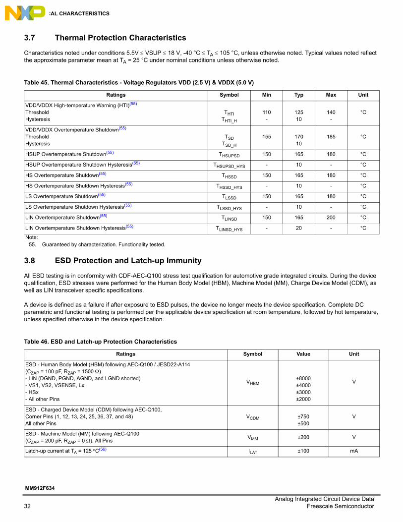
3.7 Thermal Protection Characteristics
Characteristics noted under conditions 5.5V VSUP 18 V, -40 °C TA 105 °C, unless otherwise noted. Typical values noted reflect the approximate parameter mean at TA = 25 °C under nominal conditions unless otherwise noted.
3.8 ESD Protection and Latch-up Immunity
All ESD testing is in conformity with CDF-AEC-Q100 stress test qualification for automotive grade integrated circuits. During the device qualification, ESD stresses were performed for the Human Body Model (HBM), Machine Model (MM), Charge Device Model (CDM), as well as LIN transceiver specific specifications.
A device is defined as a failure if after exposure to ESD pulses, the device no longer meets the device specification. Complete DC parametric and functional testing is performed per the applicable device specification at room temperature, followed by hot temperature, unless specified otherwise in the device specification.
HSUP Overtemperature Shutdown(55) THSUPSD 150 165 180 °C
HSUP Overtemperature Shutdown Hysteresis(55) THSUPSD_HYS - 10 - °C
HS Overtemperature Shutdown(55) THSSD 150 165 180 °C
HS Overtemperature Shutdown Hysteresis(55) THSSD_HYS - 10 - °C
LS Overtemperature Shutdown(55) TLSSD 150 165 180 °C
LS Overtemperature Shutdown Hysteresis(55) TLSSD_HYS - 10 - °C
LIN Overtemperature Shutdown(55) TLINSD 150 165 200 °C
LIN Overtemperature Shutdown Hysteresis(55) TLINSD_HYS - 20 - °C
Note:55. Guaranteed by characterization. Functionality tested.
Table 46. ESD and Latch-up Protection Characteristics
Ratings Symbol Value Unit
ESD - Human Body Model (HBM) following AEC-Q100 / JESD22-A114(CZAP = 100 pF, RZAP = 1500 )- LIN (DGND, PGND, AGND, and LGND shorted)- VS1, VS2, VSENSE, Lx- HSx- All other Pins
VHBM±8000±4000±3000±2000
V
ESD - Charged Device Model (CDM) following AEC-Q100, Corner Pins (1, 12, 13, 24, 25, 36, 37, and 48)All other Pins
VCDM ±750±500
V
ESD - Machine Model (MM) following AEC-Q100(CZAP = 200 pF, RZAP = 0 ), All Pins
VMM ±200 V
Latch-up current at TA = 125 C(56) ILAT ±100 mA
Analog Integrated Circuit Device Data32 Freescale Semiconductor
MM912F634
ELECTRICAL CHARACTERISTICS
3.9 Additional Test Information ISO7637-2
For immunity against transients for the LIN, Lx, and VBAT is specified according to the LIN Conformance Test Specification - Section LIN EMC Test Specification refer to the LIN Conformance Test Certification Report - available as a separate document from ISO.
ESD GUN - LIN Conformance Test Specification(58), unpowered, contact discharge, CZAP= 150 pF, RZAP = 330 .- LIN (with or without bus filter CBUS=220 pF)- VS1, VS2 with CVS- Lx with serial RLX
±15000±20000±6000
V
ESD GUN - IEC 61000-4-2 Test Specification(59), unpowered, contact discharge, CZAP= 150 pF, RZAP = 330 - LIN (with or without bus filter CBUS=220 pF)- VSENSE with serial RVSENSE
(57)
- VS1, VS2 with CVS- Lx with serial RLX
±8000±8000±8000±8000
V
ESD GUN - ISO10605 Test Specification(59), unpowered, contact discharge, CZAP= 150 pF, RZAP = 2.0 k- LIN (with or without bus filter CBUS=220pF)- VSENSE with serial RVSENSE
(57)
- VS1, VS2 with CVS- Lx with serial RLX
±6000±6000±6000±6000
V
ESD GUN - ISO10605 Test Specification(59), powered, contact discharge, CZAP= 330 pF, RZAP = 2.0 k- LIN (with or without bus filter CBUS=220 pF)- VSENSE with serial RVSENSE
(57)
- VS1, VS2 with CVS- Lx with serial RLX
±8000±8000±8000±8000
V
Note:56. Input Voltage Limit = -2.5 to 7.5 V.57. With CVBAT (10…100 nF) as part of the battery path.58. Certification available on request59. Tested internally only; certification pending
Table 46. ESD and Latch-up Protection Characteristics (continued)
Ratings Symbol Value Unit
Analog Integrated Circuit Device DataFreescale Semiconductor 33
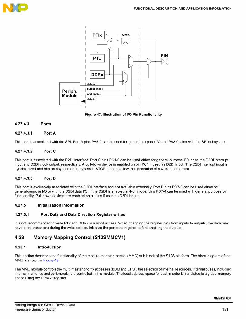
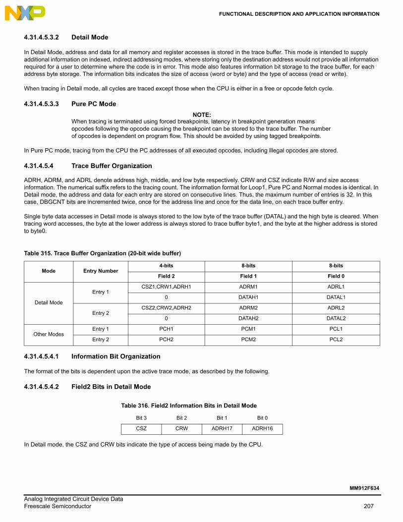
FUNCTIONAL DESCRIPTION AND APPLICATION INFORMATION
4 Functional Description and Application Information
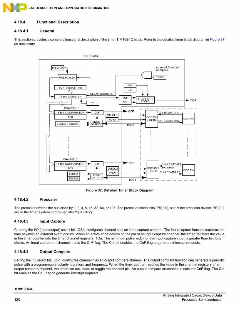
4.1 Introduction
This chapter describes the MM912F634 dual die device functions on a block by block base. To distinguish between the module location being the MCU die or the analog die, the following symbols are shown on all module cover pages:
The documented module is physically located on the Analog die. This applies to Section 4.2, “MM912F634 - Analog Die Overview" through Section 4.25, “MM912F634 - Analog Die Trimming".
The documented module is physically located on the Microcontroller die. This applies to Section 4.26, “MM912F634 - MCU Die Overview" through Section 4.38, “Serial Peripheral Interface (S12SPIV4)".
Sections concerning both dies or the complete device does not have a specific indication.
4.1.1 Device Register Maps
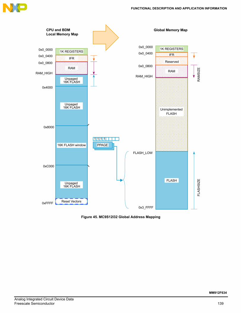
Table 47 shows the device register memory map overview for the 32 kByte MCU die (MC9S12I32).
NOTEReserved register space shown in Table 47 is not allocated to any module. This register space is reserved for future use, and shows as grayed areas in tables throughout this document. Writing to these locations has no effect. Read access to these locations returns zero.
Table 47. Device Register Memory Map Overview
Address Module Size (Bytes)
0x0000–0x0007 PIM (port integration module) 8
0x0008–0x0019 Reserved 18
0x001A–0x001B Part ID register 2
0x001C–0x001E Reserved 3
0x001F INT (interrupt module) 1
0x0020–0x002F DBG (debug module) 16
0x0030-0x0033 MMC (memory map control) 4
0x0034–0x003B CRG (clock and reset generator) 8
0x003C–0x003D RTI (real time interrupt) 2
0x003E–0x003F COP (computer operating properly) 2
0x0040–0x00D7 Reserved 152
0x00D8–0x00DF D2DI (die 2 die initiator) 8
0x00E0–0x00E7 Reserved 8
0x00E8-0x00EF SPI (serial peripheral interface) 8
0x00F0–0x00FF Reserved 16
0x0100–0x0113 FTSR control registers 20
0x0114–0x011F Reserved 12
0x0120–0x0123 PIM (port integration module) 4
0x0124–0x01FF Reserved 220
ANALOGMCU
ANALOGMCU
Analog Integrated Circuit Device Data34 Freescale Semiconductor
MM912F634
FUNCTIONAL DESCRIPTION AND APPLICATION INFORMATION
4.1.2 Detailed Module Register Maps
Table 48 to Table 65 show the detailed module maps of the MM912F634 MCU die.
0x0200-0x02FF D2DI (die 2 die initiator, blocking access window) 256
0x0300–0x03FF D2DI (die 2 die initiator, non-blocking access window) 256
Table 48. 0x0000–0x0017 Port Integration Module (PIM) 1of 2
Address Name Bit 7 Bit 6 Bit 5 Bit 4 Bit 3 Bit 2 Bit 1 Bit 0
0x0000 PTAR 0 0
PTA5 PTA4 PTA3 PTA2 PTA1 PTA 0W
0x0001 ReservedR 0 0 0 0 0 0 0 0
W
0x0002 DDRAR 0 0
DDRA5 DDRA4 DDRA3 DDRA2 DDRA1 DDRA0W
0x0003 ReservedR 0 0 0 0 0 0 0 0
W
0x0004 PTCR 0 0 0 0 0 0
PTC1 PTC0W
0x0005 PTDR
PTD7 PTD6 PTD5 PTD4 PTD3 PTD2 PTD1 PTD0W
0x0006 DDRCR 0 0 0 0 0 0
DDRC1 DDRC0W
0x0007 DDRDR
DDRD7 DDRD6 DDRD5 DDRD4 DDRD3 DDRD2 DDRD1 DDRD0W
0x0008-0x0017
ReservedR 0 0 0 0 0 0 0 0
W
Table 49. 0x0018–0x001E Miscellaneous Peripheral
Address Name Bit 7 Bit 6 Bit 5 Bit 4 Bit 3 Bit 2 Bit 1 Bit 0
Analog Integrated Circuit Device DataFreescale Semiconductor 35
MM912F634
FUNCTIONAL DESCRIPTION AND APPLICATION INFORMATION
Table 50. 0x001F Interrupt Module (S12SINT)
0x001F IVBRR
IVB_ADDR[7:0]W
Table 51. 0x0020–0x002F Debug Module (S12XDBG)
Address Name Bit 7 Bit 6 Bit 5 Bit 4 Bit 3 Bit 2 Bit 1 Bit 0
0x0020 DBGC1R
ARM0 0
BDM DBGBRK0
COMRVW TRIG
0x0021 DBGSRR TBF(60) 0 0 0 0 SSF2 SSF1 SSF0
W
0x0022 DBGTCRR 0
TSOURCE0 0
TRCMOD0
TALIGNW
0x0023 DBGC2R 0 0 0 0 0 0
ABCMW
0x0024 DBGTBHR Bit 15 Bit 14 Bit 13 Bit 12 Bit 11 Bit 10 Bit 9 Bit 8
W
0x0025 DBGTBLR Bit 7 Bit 6 Bit 5 Bit 4 Bit 3 Bit 2 Bit 1 Bit 0
W
0x0026 DBGCNTR TBF(60) 0 CNT
W
0x0027 DBGSCRXR 0 0 0 0 0
SC2 SC1 SC0W
0x0027 DBGMFRR 0 0 0 0 0 MC2 MC1 MC0
W
0x0028(61) DBGACTLR 0
NDB TAG BRK RW RWE0
COMPEW
0x0028(62) DBGBCTLR
SZE SZ TAG BRK RW RWE0
COMPEW
0x0028(63) DBGCCTLR 0 0
TAG BRK RW RWE0
COMPEW
0x0029 DBGXAHR 0 0 0 0 0 0
Bit 17 Bit 16W
0x002A DBGXAMR
Bit 15 14 13 12 11 10 9 Bit 8W
0x002B DBGXALR
Bit 7 6 5 4 3 2 1 Bit 0W
0x002C DBGADHR
Bit 15 14 13 12 11 10 9 Bit 8W
0x002D DBGADLR
Bit 7 6 5 4 3 2 1 Bit 0W
Analog Integrated Circuit Device Data36 Freescale Semiconductor
MM912F634
FUNCTIONAL DESCRIPTION AND APPLICATION INFORMATION
0x002E DBGADHMR
Bit 15 14 13 12 11 10 9 Bit 8W
0x002F DBGADLMR
Bit 7 6 5 4 3 2 1 Bit 0W
Note:60. This bit is visible at DBGCNT[7] and DBGSR[7]61. This represents the contents if the Comparator A control register is blended into this address.62. This represents the contents if the Comparator B control register is blended into this address.63. This represents the contents if the Comparator C control register is blended into this address.
Table 52. 0x0030–0x0033 Module Mapping Control (S12SMMC)
Address Name Bit 7 Bit 6 Bit 5 Bit 4 Bit 3 Bit 2 Bit 1 Bit 0
0x0030 PPAGER 0 0 0 0
PIX3 PIX2 PIX1 PIX0W
0x0031 DIRECTR
DP15 DP14 DP13 DP12 DP11 DP10 DP9 DP8W
0x0032 MODER
MODC0 0 0 0 0 0 0
W
0x0033 MMCCTL1R 0 0 0 0 0 0 0
IFRONW
Table 53. 0x0034–0x003B Clock and Reset Generator (CRG)
Address Name Bit 7 Bit 6 Bit 5 Bit 4 Bit 3 Bit 2 Bit 1 Bit 0
Note:64. Registers not shown are reserved and must not be accessed.
Table 65. Analog die Registers(64) - 0x0200–0x02FF D2D Blocking Access (D2DI) 2 of 3/0x0300–0x03FF D2D Non Blocking Access (D2DI) 3 of 3 (continued)
Offset Name 7 6 5 4 3 2 1 0
Analog Integrated Circuit Device Data46 Freescale Semiconductor
MM912F634
FUNCTIONAL DESCRIPTION AND APPLICATION INFORMATION
4.2 MM912F634 - Analog Die Overview
4.2.1 Introduction
The MM912F634 analog die implements all system base functionality to operate the integrated microcontroller, and delivers application specific actuator control as well as input capturing.
4.2.2 System Registers
4.2.2.1 Silicon Revision Register (SRR)
NOTERefer to the MM912F634ER - Mask set errata document for details on the analog die mask revisions.
4.2.3 Analog Die Options
NOTEThis document describes the features and functions of option 1 (all modules available and tested). Beyond this chapter, there is no additional note or differentiation between the different implementations.
The following section describes the differences between analog die options 1 and 2.
Table 66. Silicon Revision Register (SRR)
Offset(65)0xF4 Access: User read
7 6 5 4 3 2 1 0
R 0 0 0 0 FMREV MMREV
W
Note:65. Offset related to 0x0200 for blocking access and 0x300 for non blocking access within the global address space.
Table 67. SRR - Register Field Descriptions
Field Description
3-2FMREV MM912F634 analog die Silicon Revision Register - These bits represent the revision of Silicon of the analog die. They are incremented
for every full mask or metal mask issued of the device.One number is set for one revision of the silicon of the analog die.1-0
MMREV
Table 68. Analog Die Options
Feature Option 1 Option 2
Current Sense Module YES NO
Wake Up Inputs (Lx) L0…L5 L0.L3
ANALOGMCU
Analog Integrated Circuit Device DataFreescale Semiconductor 47
Analog Integrated Circuit Device Data48 Freescale Semiconductor
MM912F634
FUNCTIONAL DESCRIPTION AND APPLICATION INFORMATION
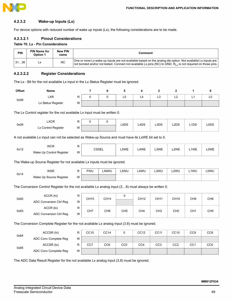
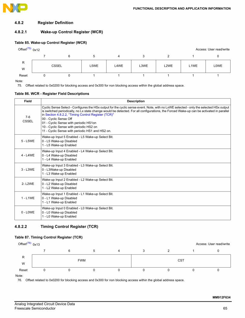
4.2.3.2 Wake-up Inputs (Lx)
For device options with reduced number of wake up inputs (Lx), the following considerations are to be made.
4.2.3.2.1 Pinout Considerations
4.2.3.2.2 Register Considerations
The Lx - Bit for the not available Lx input in the Lx Status Register must be ignored.
The Lx Control register for the not available Lx input must be written 0.
A not available Lx input can not be selected as Wake-up Source and must have its LxWE bit set to 0.
The Wake-up Source Register for not available Lx inputs must be ignored.
The Conversion Control Register for the not available Lx analog input (3…8) must always be written 0.
The Conversion Complete Register for the not available Lx analog input (3.8) must be ignored.
The ADC Data Result Register for the not available Lx analog input (3.8) must be ignored.
Table 70. Lx - Pin Considerations
PINPIN Name for
Option 1New PIN
nameComment
31…36 Lx NCOne or more Lx wake up inputs are not available based on the analog die option. Not available Lx inputs are not bonded and/or not tested. Connect not available Lx pins (NC) to GND. RLx is not required on those pins.
Offset Name 7 6 5 4 3 2 1 0
0x08LXR R 0 0 L5 L4 L3 L2 L1 L0
Lx Status Register W
0x09LXCR R 0 0
L5DS L4DS L3DS L2DS L1DS L0DSLx Control Register W
0x12WCR R
CSSEL L5WE L4WE L3WE L2WE L1WE L0WEWake Up Control Register W
Analog Integrated Circuit Device DataFreescale Semiconductor 49
MM912F634
FUNCTIONAL DESCRIPTION AND APPLICATION INFORMATION
4.2.3.2.3 Functional Considerations
For the not available Lx inputs, the following functions are limited:
• No Wake-up feature / Cyclic Sense• No Digital Input• No Analog Input and conversion via ADC
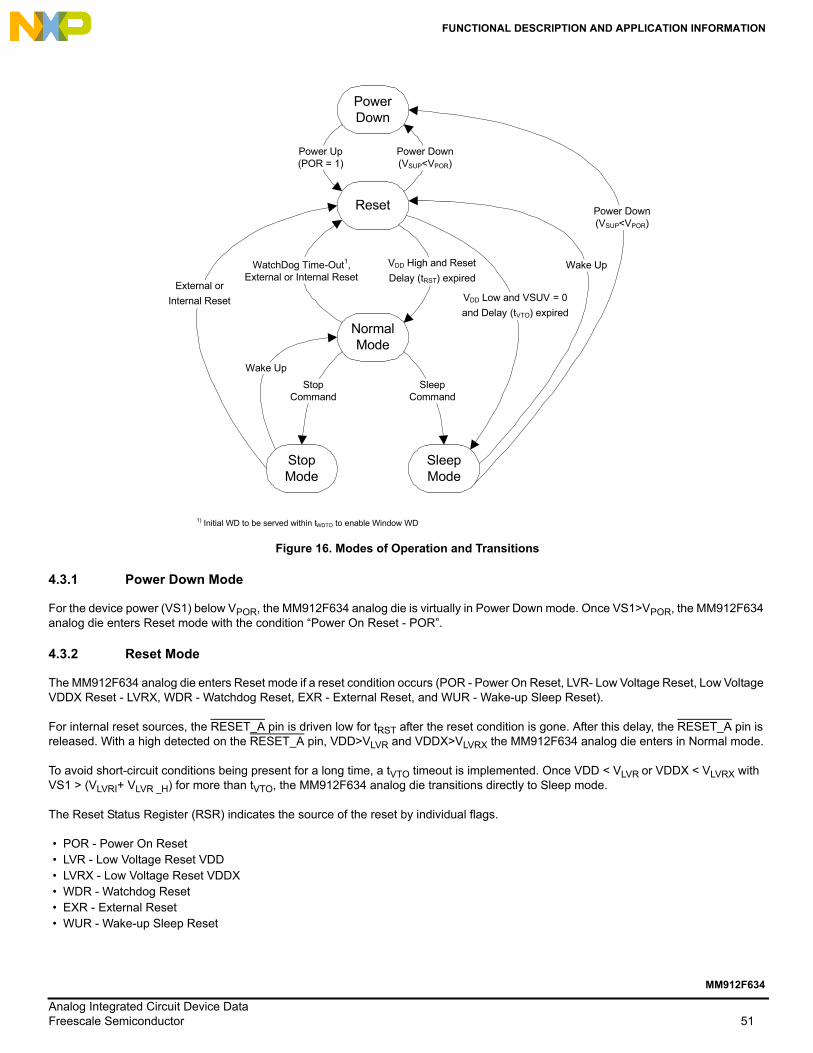
4.3 Modes of Operation
The MM912F634 analog die offers three main operating modes: Normal (Run), Stop, and Sleep. In Normal mode, the device is active and is operating under normal application conditions. In Stop mode, the voltage regulator operates with limited current capability, the external load is expected to be reduced while in Stop mode. In Sleep mode both voltage regulators are turned off (VDD = VDDX = 0 V).
Wake-up from Stop mode is indicated by an interrupt signal. Wake-up from Sleep mode changes the MM912F634 analog die into reset mode while the voltage regulator is turned back on.
The selection of the different modes is controlled by the Mode Control Register (MCR).
Figure 16 describes how transitions are done between the different operating modes.
Analog Integrated Circuit Device Data50 Freescale Semiconductor
MM912F634
FUNCTIONAL DESCRIPTION AND APPLICATION INFORMATION
Figure 16. Modes of Operation and Transitions
4.3.1 Power Down Mode
For the device power (VS1) below VPOR, the MM912F634 analog die is virtually in Power Down mode. Once VS1>VPOR, the MM912F634 analog die enters Reset mode with the condition “Power On Reset - POR”.
4.3.2 Reset Mode
The MM912F634 analog die enters Reset mode if a reset condition occurs (POR - Power On Reset, LVR- Low Voltage Reset, Low Voltage VDDX Reset - LVRX, WDR - Watchdog Reset, EXR - External Reset, and WUR - Wake-up Sleep Reset).
For internal reset sources, the RESET_A pin is driven low for tRST after the reset condition is gone. After this delay, the RESET_A pin is released. With a high detected on the RESET_A pin, VDD>VLVR and VDDX>VLVRX the MM912F634 analog die enters in Normal mode.
To avoid short-circuit conditions being present for a long time, a tVTO timeout is implemented. Once VDD < VLVR or VDDX < VLVRX with VS1 > (VLVRI+ VLVR _H) for more than tVTO, the MM912F634 analog die transitions directly to Sleep mode.
The Reset Status Register (RSR) indicates the source of the reset by individual flags.
• POR - Power On Reset• LVR - Low Voltage Reset VDD• LVRX - Low Voltage Reset VDDX• WDR - Watchdog Reset• EXR - External Reset• WUR - Wake-up Sleep Reset
Power Down
Reset
Normal Mode
Stop Mode
Sleep Mode
Power Up(POR = 1)
VDD High and Reset
Delay (tRST) expired
Wake Up
Wake Up
External or
Internal Reset
Power Down(VSUP<VPOR)
WatchDog Time-Out1, External or Internal Reset
StopCommand
SleepCommand
1) Initial WD to be served within tWDTO to enable Window WD
VDD Low and VSUV = 0
and Delay (tVTO) expired
Power Down(VSUP<VPOR)
Analog Integrated Circuit Device DataFreescale Semiconductor 51
MM912F634
FUNCTIONAL DESCRIPTION AND APPLICATION INFORMATION
See also Section 4.7, “Resets".
4.3.3 Normal Mode
In Normal mode, all MM912F634 analog die user functions are active and can be controlled by the D2D Interface. Both regulators (VDD and VDDX) are active and operate with full current capability.
Once entered in Normal mode, the Watchdog operates as a simple non-window watchdog with an initial timeout (tIWDTO) to be reset via the D2D Interface. After the initial reset, the watchdog operates in standard window mode. See Section 4.9, “Window Watchdog" for details.
4.3.4 Stop Mode
NOTETo avoid any pending analog die interrupts prevent the MCU from entering MCU stop resulting in unexpected system behavior, the analog die IRQ sources should be disabled and the corresponding flags be cleared before entering stop.
The Stop mode allows reduced current consumption with fast startup time. In this mode, both voltage regulators (VDD and VDDX) are active, with limited current drive capability. In this condition, the MCU is supposed to operate in Low Power mode (STOP or WAIT).
The device can enter in Stop mode by configuring the Mode Control Register (MCR) via the D2D Interface. The MCU has to enter a Low Power mode immediately afterwards executing the STOP or WAIT instruction. The Wake-up Source Register (WSR) has to be read after a wake-up condition in order to execute a new STOP mode command. Two base clock cycles (fBASE) delay are required between WSR read and MCR write.
While in Stop mode, the MM912F634 analog die wakes up on the following sources:
• Lx - Wake-up (maskable with selectable cyclic sense)• Forced Wake-up (configurable timeout)• LIN Wake-up• D2D Wake-up (special command)
After Wake-up from the sources listed above, the device transitions to Normal mode.
Reset wakes up the device directly to Reset mode.
See Section 4.8, “Wake-up / Cyclic Sense" for details.
4.3.5 Sleep Mode
The Sleep mode allows very low current consumption. In this mode, both voltage regulators (VDD and VDDX) are inactive.
The device can enter into Sleep mode by configuring the Mode Control Register (MCR) via the D2D- Interface. During Sleep mode, all unused internal blocks are deactivated to allow the lowest possible consumption. Power consumption decreases further if the Cyclic Sense or Forced Wake-up feature are disabled. While in Sleep mode, the MM912F634 analog die wakes up on the following sources:
• Lx - Wake-up (maskable with selectable cyclic sense)• Forced Wake-up (configurable timeout)• LIN Wake-up
After Wake-up from the sources listed above or a reset condition, the device transitions to Reset mode.
See Section 4.8, “Wake-up / Cyclic Sense" for details.
Analog Integrated Circuit Device Data52 Freescale Semiconductor
MM912F634
FUNCTIONAL DESCRIPTION AND APPLICATION INFORMATION
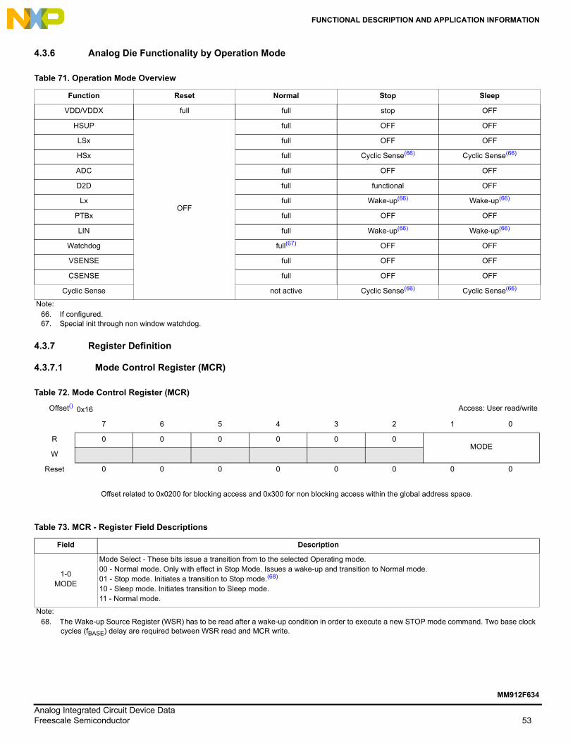
4.3.6 Analog Die Functionality by Operation Mode
4.3.7 Register Definition
4.3.7.1 Mode Control Register (MCR)
Table 71. Operation Mode Overview
Function Reset Normal Stop Sleep
VDD/VDDX full full stop OFF
HSUP
OFF
full OFF OFF
LSx full OFF OFF
HSx full Cyclic Sense(66) Cyclic Sense(66)
ADC full OFF OFF
D2D full functional OFF
Lx full Wake-up(66) Wake-up(66)
PTBx full OFF OFF
LIN full Wake-up(66) Wake-up(66)
Watchdog full(67) OFF OFF
VSENSE full OFF OFF
CSENSE full OFF OFF
Cyclic Sense not active Cyclic Sense(66) Cyclic Sense(66)
Note:66. If configured.67. Special init through non window watchdog.
Table 72. Mode Control Register (MCR)
Offset() 0x16 Access: User read/write
7 6 5 4 3 2 1 0
R 0 0 0 0 0 0MODE
W
Reset 0 0 0 0 0 0 0 0
Offset related to 0x0200 for blocking access and 0x300 for non blocking access within the global address space.
Table 73. MCR - Register Field Descriptions
Field Description
1-0MODE
Mode Select - These bits issue a transition from to the selected Operating mode.00 - Normal mode. Only with effect in Stop Mode. Issues a wake-up and transition to Normal mode.01 - Stop mode. Initiates a transition to Stop mode.(68)
10 - Sleep mode. Initiates transition to Sleep mode.11 - Normal mode.
Note:68. The Wake-up Source Register (WSR) has to be read after a wake-up condition in order to execute a new STOP mode command. Two base clock
cycles (fBASE) delay are required between WSR read and MCR write.
Analog Integrated Circuit Device DataFreescale Semiconductor 53
MM912F634
FUNCTIONAL DESCRIPTION AND APPLICATION INFORMATION
4.4 Power Supply
The MM912F634 analog die supplies VDD (2.5 V), VDDX (5.0 V), and HSUP, based on the supply voltage applied to the VS1 pin. VDD is cascaded of the VDDX regulator. To separate the High-side outputs from the main power supply, the VS2 pin does only power the High-side drivers. Both supply pins have to be externally protected against reverse battery conditions. To supply external Hall Effect Sensors, the HSUP pin supplies a switchable regulated supply. See Section 4.10, “Hall Sensor Supply Output - HSUP".
A reverse battery protected input (VSENSE) is implemented to measure the Battery Voltage directly. A serial resistor (RVSENSE) is required on this pin. See Section 4.22, “Supply Voltage Sense - VSENSE". In addition, the VS1 supply can be routed to the ADC (VS1SENSE) to measure the VS1 pin voltage directly. See Section 4.23, “Internal Supply Voltage Sense - VS1SENSE".
To have an independent ADC verification, the internal sleep mode bandgap voltage can be routed to the ADC (BANDGAP). As this node is independent from the ADC reference, any out of range result would indicate malfunctioning ADC or Bandgap reference. See Section 4.24, “Internal Bandgap Reference Voltage Sense - BANDGAP".
To stabilize the internal ADC reference voltage for higher precision measurements, the current limited ADC2p5 pin needs to be connected to an external filter capacitor (CADC2p5). It is not recommended to connect additional loads to this pin. See Section 4.19, “Analog Digital Converter - ADC".
The following safety features are implemented:
• LBI - Low Battery Interrupt, internally measured at VSENSE• LVI - Low Voltage Interrupt, internally measured at VS1• HVI - High Voltage Interrupt, internally measured at VS2• VROVI - Voltage Regulator Overvoltage Interrupt internally measured at VDD and VDDX• LVR - Low Voltage Reset, internally measured at VDD• LVRX - Low Voltage Reset, internally measured at VDDX• HTI - High Temperature Interrupt measured between the VDD and VDDX regulators• Overtemperature Shutdown measured between the VDD and VDDX regulators
Figure 17. MM912F634 Power Supply
VDDX (5V)Regulator
VDD (2.5V)Regulator
HSUP (18V)Regulator
HS1 & HS2
ADC
÷
VS
2
VS
1
VS
EN
SE
HSUP
HS1
HS2
VDDX
VDD
ADC 2.5VReference
VDDXINTERNAL
VDDINTERNAL
ADC2p5
CVDDX
CVDD
CADC
CHSUP
HVI
LVI
LBI
LVR
LVRXVROV
bg1p25sleep
Analog Integrated Circuit Device Data54 Freescale Semiconductor
MM912F634
FUNCTIONAL DESCRIPTION AND APPLICATION INFORMATION
4.4.1 Voltage Regulators VDD (2.5 V) & VDDX (5.0 V)
To supply the MCU die and minor additional loads two cascaded voltage regulators have been implemented, VDDX (5.0 V) and VDD (2.5 V). External capacitors (CVDD) and (CVDDX) are required for proper regulation.
4.4.2 Power Up Behavior / Power Down Behavior
To guarantee safe power up and down behavior, special dependencies are implemented to prevent unwanted MCU execution.
Figure 18 shows a standard power up and power down sequence.
Figure 18. Power-up / Down Sequence
To avoid any abnormal device behavior, it is essential to have the MCU Power on Reset (POR) block complete its start-up sequence before the analog die reset signal (RESET A) is asserted. Since the RESET A circuitry is supplied by VDDX, the voltage on the 2.5 V supply (VDD) needs to remain below the POR threshold whenever VDDX is too low to guarantee RESET A can be properly asserted (3;6). This is achieved with the following implementation.
Power-up:
• The VDD regulator is enabled after VDDX has reached the VLVRX threshold (1). • Once VDD reaches VLVR, the RESET_A is released (2).
Power-down:
• Once VDDX has reached the VLVRX threshold (4), the VDD regulator is disabled and the regulator output is actively pulled down to discharge any VDD capacitance (5). RESET_A is activated as well.
• The active discharge guarantees VDD to be below POR level before VDDX discharges below critical level for the reset circuity.
5V
VLBI / VLVI
Normal Operating Range (not to scale)
VLVRX
VLVR
VPOR_A
RESET_A
VDDX VDDVSUP
VPOR_MCU
VROVX
VROX
MCU_POR
1 4
5
6
2
MCU_POR
3
Analog Integrated Circuit Device DataFreescale Semiconductor 55
MM912F634
FUNCTIONAL DESCRIPTION AND APPLICATION INFORMATION
4.4.3 Register Definition
4.4.3.1 Voltage Control Register (VCR)
4.4.3.2 Voltage Status Register (VSR)
Table 74. Voltage Control Register (VCR)
Offset(69) 0x04 Access: User read/write
7 6 5 4 3 2 1 0
R 0 0 0VROVIE HTIE HVIE LVIE LBIE
W
Reset 0 0 0 0 0 0 0 0
Note:69. Offset related to 0x0200 for blocking access and 0x300 for non blocking access within the global address space.
Table 75. VCR - Register Field Descriptions
Field Description
4VROVIE
Voltage Regulator Overvoltage Interrupt Enable — Enables the interrupt for the Regulator Overvoltage Condition.0 - Voltage Regulator Overvoltage Interrupt is disabled1 - Voltage Regulator Overvoltage Interrupt is enabled
3HTIE
High Temperature Interrupt Enable — Enables the interrupt for the Voltage Regulator (VDD/VDDX) Temperature Warning.0 - High Temperature Interrupt is disabled1 - High Temperature Interrupt is enabled
2HVIE
High Voltage Interrupt Enable — Enables the interrupt for the VS2 - High Voltage Warning.0 - High Voltage Interrupt is disabled1 - High Voltage Interrupt is enabled
1LVIE
Low Voltage Interrupt Enable — Enables the interrupt for the VS1 - Low Voltage Warning.0 - Low Voltage Interrupt is disabled1 - Low Voltage Interrupt is enabled
0LBIE
Low Battery Interrupt Enable — Enables the interrupt for the VSENSE - Low Battery Voltage Warning.0 - Low Battery Interrupt is disabled1 - Low Battery Interrupt is enabled
Table 76. Voltage Status Register (VSR)
Offset(70)0x05 Access: User read
7 6 5 4 3 2 1 0
R 0 0 0 VROVC HTC HVC LVC LBC
W
Reset 0 0 0 0 0 0 0 0
Note:70. Offset related to 0x0200 for blocking access and 0x300 for non blocking access within the global address space.
Analog Integrated Circuit Device Data56 Freescale Semiconductor
MM912F634
FUNCTIONAL DESCRIPTION AND APPLICATION INFORMATION
4.5 Die to Die Interface - Target
The D2D Interface is the bus interface to the Microcontroller. Access to the MM912F634 analog die is controlled by the D2D Interface module. This section describes the functionality of the die-to-die target block (D2D).
4.5.1 Overview
The D2D is the target for a data transfer from the target to the initiator (MCU). The initiator provides a set of configuration registers and two memory mapped 256 Byte address windows. When writing to a window, a transaction is initiated sending a write command, followed by an 8-bit address, and the data byte or word is received from the initiator. When reading from a window, a transaction is received with the read command, followed by an 8-bit address. The target then responds with the data. The basic idea is that a peripheral located on the MM912F634 analog die, can be addressed like an on-chip peripheral.
Features:
• software transparent register access to peripherals on the MM912F634 analog die• 256 Byte address window• supports blocking read or write, as well as non-blocking write transactions• 4 bit physical bus width• automatic synchronization of the target when initiator starts driving the interface clock• generates transaction and error status as well as EOT acknowledge• providing single interrupt interface to D2D Initiator
Table 77. VSR - Register Field Descriptions
Field Description
4VROVC
Voltage Regulator Overvoltage Condition - This status bit indicates an overvoltage warning is present for at least one of the main voltage regulators (VDD or VDDX). Reading the register clears the VROVI flag if present. See Section 4.6, “Interrupts" for details. Note: This feature requires the trimming of Section 4.25.2.3, “Trimming Register 2 (CTR2)" to be done to be effective. Untrimmed devices may issue the VROVC condition including the LS turn off at normal operation.0 - No Voltage Regulator Overvoltage Condition present.1 - Voltage Regulator Overvoltage Condition present.
3HTC
High Temperature Condition - This status bit indicates a high temperature warning is present for the Voltage regulators (VDD/VDDX). Reading the register clears the HTI flag if present. See Section 4.6, “Interrupts" for details.0 - No High Temperature Condition present.1 - High Temperature Condition present.
2HVC
High Voltage Condition - This status bit indicates a high voltage warning for VS2 is present. Reading the register clears the HVI flag if present. See Section 4.6, “Interrupts" for details.0 - No High Voltage Condition present.1 - High Voltage Condition present.
1LVC
Low Voltage Condition - This status bit indicates a low voltage warning for VS1 is present. Reading the register clears the LVI flag if present. See Section 4.6, “Interrupts" for details.0 - No Low Voltage Condition present.1 - Low Voltage Condition present.
0LBC
Low Battery Condition - This status bit indicates a low voltage warning for VSENSE is present. Reading the register clears the LBI flag if present. See Section 4.6, “Interrupts" for details.0 - No Low Battery Condition present.1 - Low Battery Condition present.
Analog Integrated Circuit Device DataFreescale Semiconductor 57
MM912F634
FUNCTIONAL DESCRIPTION AND APPLICATION INFORMATION
4.5.2 Low Power Mode Operation
The D2D module is disabled in SLEEP mode. In Stop mode, the D2DINT signal is used to wake-up a powered down MCU. As the MCU could wake up without the MM912F634 analog die, a special command is recognized as a wake-up event during Stop mode. See Section 4.3, “Modes of Operation".
4.5.2.1 Normal Mode / Stop Mode
NOTEThe maximum allowed clock speed of the interface is limited to fD2D.
While in Normal or Stop mode, D2DCLK acts as input only with pull present. D2D[3:0] operates as an input/output with pull-down always present. D2DINT acts as output only.
4.5.2.2 Sleep Mode
While in Sleep mode, all Interface data pins are pulled down to DGND to reduce power consumption.
4.6 Interrupts
Interrupts are used to signal a microcontroller that a peripheral needs to be serviced. While in Stop mode, the interrupt signal is used to signal Wake-up events. The interrupts are signaled by an active high level of the D2DINT pin, which remains high until the interrupt is acknowledged via the D2D-Interface. Interrupts are only asserted while in Normal mode.
4.6.1 Interrupt Source Identification
Once an Interrupt is signalized, there are two options to identify the corresponding source(s).
4.6.1.1 Interrupt Source Mirror
NOTEThe VSI - Voltage Status Interrupt combines the five status flags for the Low Battery Interrupt, Low Voltage Interrupt, High Voltage Interrupt, Voltage Regulator Overvoltage Interrupt, and the Voltage Regulator High Temperature Interrupt. The specific source can be identified by reading the Voltage Status Register - VSR.
All Interrupt sources in MM912F634 analog die are mirrored to a special Interrupt Source Register (ISR). This register is read only and indicates all currently pending Interrupts. Reading this register does not acknowledge any interrupt. An additional D2D access is necessary to serve the specific module.
4.6.1.1.1 Interrupt Source Register (ISR)
Table 78. Interrupt Source Register (ISR)
Offset(71)0x00 (0x00 and 0x01 for 8Bit access) Access: User read
15 14 13 12 11 10 9 8 7 6 5 4 3 2 1 0
R 0 0 HOT LSOT HSOT LINOT SCI RX TX ERR TOV CH3 CH2 CH1 CH0 VSI
W
Note:71. Offset related to 0x0200 for blocking access and 0x300 for non blocking access within the global address space.
Analog Integrated Circuit Device Data58 Freescale Semiconductor
MM912F634
FUNCTIONAL DESCRIPTION AND APPLICATION INFORMATION
4.6.1.2 Interrupt Vector Emulation by Priority
To allow a vector based interrupt handling by the MCU, the number of the highest prioritized interrupt pending is returned in the Interrupt Vector Register. To allow an offset based vector table, the result is pre-shifted (multiple of 2). Reading this register does not acknowledge an interrupt. An additional D2D access is necessary to serve the specific module.
4.6.1.2.1 Interrupt Vector Register (IVR)
The following table is listing all MM912F634 analog die interrupt sources with the corresponding priority.
Table 79. ISR - Register Field Descriptions
Field Description
0 - VSI
VSI - Voltage Status Interrupt combining the following sources: • Low Battery Interrupt • Low Voltage Interrupt • High Voltage Interrupt • Voltage Regulator Overvoltage Interrupt • Voltage Regulator High Temperature Interrupt
1 - CH0 CH0 - TIM Channel 0 Interrupt
2 - CH1 CH1 - TIM Channel 1 Interrupt
3 - CH2 CH2 - TIM Channel 2 Interrupt
4 - CH3 CH3 - TIM Channel 3 Interrupt
5 - TOV TOV - Timer Overflow Interrupt
6 - ERR ERR - SCI Error Interrupt
7 - TX TX - SCI Transmit Interrupt
8 - RX RX - SCI Receive Interrupt
9 - SCI SCI - ADC Sequence Complete Interrupt
10 - LINOT LINOT - LIN Driver Overtemperature Interrupt
Note:72. Offset related to 0x0200 for blocking access and 0x300 for non blocking access within the global address space.
Table 81. IVR - Register Field Descriptions
Field Description
5:0IRQ
Represents the highest prioritized interrupt pending. See Table 82 In case no interrupt is pending, the result is 0.
Analog Integrated Circuit Device DataFreescale Semiconductor 59
MM912F634
FUNCTIONAL DESCRIPTION AND APPLICATION INFORMATION
4.6.2 Interrupt Sources
4.6.2.1 Voltage Status Interrupt (VSI)
The Voltage Status Interrupt - VSI combines the five interrupt sources of the Voltage Status Register. It is only available in the Interrupt Source Register (ISR). Acknowledge the interrupt by reading the Voltage Status Register - VSR. To issue a new interrupt, the condition has to vanish and occur again. See Section 4.4, “Power Supply" for details on the Voltage Status Register including masking information.
4.6.2.2 Low Voltage Interrupt (LVI)
Acknowledge the interrupt by reading the Voltage Status Register - VSR. To issue a new interrupt, the condition has to vanish and occur again. See Section 4.4, “Power Supply" for details on the Voltage Status Register including masking information.
4.6.2.3 Voltage Regulator High Temperature Interrupt (HTI)
Acknowledge the interrupt by reading the Voltage Status Register - VSR. To issue a new interrupt, the condition has to vanish and occur again. See Section 4.4, “Power Supply" for details on the Voltage Status Register including masking information.
4.6.2.4 Low Battery Interrupt (LBI)
Acknowledge the interrupt by reading the Voltage Status Register - VSR. To issue a new interrupt, the condition has to vanish and occur again. See Section 4.4, “Power Supply" for details on the Voltage Status Register including masking information.
4.6.2.5 TIM Channel 0 Interrupt (CH0)
See Section 4.18, “Basic Timer Module - TIM (TIM16B4C)".
Table 82. Interrupt Source Priority
Interrupt Source IRQ Priority
no interrupt pending or wake-up from Stop mode 0x00 1 (highest)
LVI - Low Voltage Interrupt 0x02 2
HTI - Voltage Regulator High Temperature Interrupt 0x04 3
LBI - Low Battery Interrupt 0x06 4
CH0 - TIM Channel 0 Interrupt 0x08 5
CH1 - TIM Channel 1 Interrupt 0x0A 6
CH2 - TIM Channel 2 Interrupt 0x0C 7
CH3 - TIM Channel 3 Interrupt 0x0E 8
TOV - Timer Overflow Interrupt 0x10 9
ERR - SCI Error Interrupt 0x12 10
TX - SCI Transmit Interrupt 0x14 11
RX - SCI Receive Interrupt 0x16 12
SCI - ADC Sequence Complete Interrupt 0x18 13
LINOT - LIN Driver Overtemperature Interrupt 0x1A 14
VROVI - Voltage Regulator Overvoltage Interrupt 0x24 19 (lowest)
Analog Integrated Circuit Device Data60 Freescale Semiconductor
MM912F634
FUNCTIONAL DESCRIPTION AND APPLICATION INFORMATION
4.6.2.6 TIM Channel 1 Interrupt (CH1)
See Section 4.18, “Basic Timer Module - TIM (TIM16B4C)".
4.6.2.7 TIM Channel 2 Interrupt (CH2)
See Section 4.18, “Basic Timer Module - TIM (TIM16B4C)".
4.6.2.8 TIM Channel 3 Interrupt (CH3)
See Section 4.18, “Basic Timer Module - TIM (TIM16B4C)".
4.6.2.9 TIM Timer Overflow Interrupt (TOV)
See Section 4.18, “Basic Timer Module - TIM (TIM16B4C)".
4.6.2.10 SCI Error Interrupt (ERR)
See Section 4.15, “Serial Communication Interface (S08SCIV4)".
4.6.2.11 SCI Transmit Interrupt (TX)
See Section 4.15, “Serial Communication Interface (S08SCIV4)".
4.6.2.12 SCI Receive Interrupt (RX)
See Section 4.15, “Serial Communication Interface (S08SCIV4)".
4.6.2.13 LIN Driver Overtemperature Interrupt (LINOT)
Acknowledge the interrupt by reading the LIN Register - LINR. To issue a new interrupt, the condition has to vanish and occur again. See Section 4.14, “LIN Physical Layer Interface - LIN" for details on the LIN Register including masking information.
Acknowledge the interrupt by reading the High-side Status Register - HSSR. To issue a new interrupt, the condition has to vanish and occur again. See Section 4.11, “High-side Drivers - HS" for details on the High-side Status Register including masking information.
Acknowledge the interrupt by reading the Low-side Status Register - LSSR. To issue a new interrupt, the condition has to vanish and occur again. See Section 4.12, “Low-side Drivers - LSx" for details on the Low-side Status Register including masking information.
4.6.2.16 HSUP Overtemperature Interrupt (HOT)
Acknowledge the interrupt by reading the Hall Supply Register - HSR. To issue a new interrupt, the condition has to vanish and occur again. See Section 4.10, “Hall Sensor Supply Output - HSUP" for details on the Hall Supply Register including masking information.
4.6.2.17 High Voltage Interrupt (HVI)
Acknowledge the interrupt by reading the Voltage Status Register - VSR. To issue a new interrupt, the condition has to vanish and occur again. See Section 4.4, “Power Supply" for details on the Voltage Status Register including masking information.
4.6.2.18 Voltage Regulator Overvoltage Interrupt (VROVI)
Acknowledge the interrupt by reading the Voltage Status Register - VSR. To issue a new interrupt, the condition has to vanish and occur again. See Section 4.4, “Power Supply" for details on the Voltage Status Register including masking information.
Analog Integrated Circuit Device DataFreescale Semiconductor 61
MM912F634
FUNCTIONAL DESCRIPTION AND APPLICATION INFORMATION
4.7 Resets
To protect the system during critical events, the MM912F634 analog die drives the RESET_A pin low during the presence of the reset condition. In addition, the RESET_A pin is monitored for external reset events. To match the MCU, the RESET_A pin is based on the VDDX voltage level.
After an internal reset condition has gone, the RESET_A stays low for an additional time tRST before being released. Entering reset mode causes all MM912F634 analog die registers to be initialized to their RESET default. The only registers with valid information are the Reset Status Register (RSR) and the Wake-up Source Register (WUS).
4.7.1 Reset Sources
In the MM912F634 six reset sources exist.
4.7.1.1 POR - Analog Die Power On Reset
To indicate the device power supply (VS1) was below VPOR or the MM912F634 analog die was powered up, the POR condition is set. See Section 4.3, “Modes of Operation".
4.7.1.2 LVR - Low Voltage Reset - VDD
With the VDD voltage regulator output voltage falling below VLVR, the Low Voltage Reset condition becomes present. As the VDD Regulator is shutdown once a LVRX condition is detected, The actual cause could be also a low voltage condition at the VDDX regulator. See Section 4.4, “Power Supply".
4.7.1.3 LVRX - Low Voltage Reset - VDDX
With the VDDX voltage regulator output voltage falling below VLVRX, the Low Voltage Reset condition becomes present. See Section 4.4, “Power Supply".
4.7.1.4 WUR - Wake-up Reset
While in Sleep mode, any active wake-up event causes a MM912F634 analog die transition from Sleep to Reset Mode. To determine the wake-up source, refer to Section 4.8, “Wake-up / Cyclic Sense".
4.7.1.5 EXR - External Reset
Any low level voltage at the RESET_A pin with a duration > tRSTDF issues an External Reset event. This reset source is also active in Stop mode.
4.7.1.6 WDR - Watchdog Reset
Any incorrect serving if the MM912F634 analog die Watchdog results in a Watchdog Reset. Refer to the Section 4.9, “Window Watchdog" for details.
4.7.2 Register Definition
4.7.2.1 Reset Status Register (RSR)
Table 83. Reset Status Register (RSR)
Offset(73)0x15 Access: User read
7 6 5 4 3 2 1 0
R 0 0 WDR EXR WUR LVRX LVR POR
W
Note:73. Offset related to 0x0200 for blocking access and 0x300 for non blocking access within the global address space.
Analog Integrated Circuit Device Data62 Freescale Semiconductor
MM912F634
FUNCTIONAL DESCRIPTION AND APPLICATION INFORMATION
Reading the Reset Status register clears the information inside. Writing has no effect. LVR and LVRX are masked when POR or WUR are set.
4.8 Wake-up / Cyclic Sense
To wake-up the MM912F634 analog die from Stop or Sleep mode, several wake-up sources are implemented. As described in Section 4.3, “Modes of Operation", a wake-up from Stop mode results in an interrupt (D2DINT) to the MCU combined with a transition to Normal mode. A wake-up from Sleep mode results in a transition to Reset mode. In any case, the source of the wake-up can be identified by reading the Wake-up Source Register (WSR). The Wake-up Source Register (WSR) has to be read after a wake-up condition in order to execute a new STOP mode command. Two base clock cycles (fBASE) delay are required between the WSR read and MCR write.
In general, there are the following seven main wake-up sources:
• Wake-up by a state change of one of the Lx inputs• Wake-up by a state change of one of the Lx inputs during a cyclic sense• Wake-up due to a forced wake-up• Wake-up by the LIN module• Wake-up by D2D interface (Stop mode only)• Wake-up due to internal / external Reset (Stop mode only)• Wake-up due to loss of supply voltage (Sleep mode only)
Figure 19. Wake-up Sources
Table 84. RSR - Register Field Descriptions
Field Description
5 - WDR Watchdog Reset - Reset caused by an incorrect serving of the watchdog.
4 - EXR External Reset - Reset caused by the RESET_A pin driven low externally for > tRSTDF
3 - WURWake-up Reset - Reset caused by a wake-up from Sleep mode. To determine the wake-up source, refer to Section 4.8, “Wake-up / Cyclic Sense".
2 - LVRX Low Voltage Reset VDDX - Reset caused by a low voltage condition monitored at the VDDX output.
1 - LVR Low Voltage Reset VDD - Reset caused by a low voltage condition monitored at the VDD output.(74)
0 - POR Power On Reset - Supply Voltage was below VPOR.
Note:74. As the VDD Regulator is shutdown once a LVRX condition is detected, The actual cause could be also a low voltage condition at the VDDX
regulator.
LIN Bus
HS1
HS2
L1
L2
L3
L4
L5
VSUP
LIN
D2DINT
D2DCLK
D2D3
D2D2
D2D1
D2D0
Wake Up Module
D2DWake Up
LIN Wake Up
Lx – Wake Up
Cyclic Sense / Forced Wake Up TimerForced
Wake Up
Cyclic Wake Up
L0
Analog Integrated Circuit Device DataFreescale Semiconductor 63
MM912F634
FUNCTIONAL DESCRIPTION AND APPLICATION INFORMATION
4.8.1 Wake-up Sources
4.8.1.1 Lx - Wake-up (Cyclic Sense Disabled)
Any state digital change on a Wake-up Enabled Lx input issues a wake-up. In order to select and activate a Wake-up Input (Lx), the Wake-up Control Register (WCR) must be configured with appropriate LxWE inputs enabled or disabled before entering low power mode. The Lx - Wake-up may be combined with the Forced Wake-up.
Note: Selecting a Lx Input for wake-up disables a selected analog input once entering low power mode.
4.8.1.2 Lx - Cyclic Sense Wake-up
NOTEOnce Cyclic Sense is configured (CSSEL!=0), the state change is only recognized from one cyclic sense event to the next.
The additional accuracy of the cyclic sense cycle by the WD clock trimming is only active during STOP mode. There is no trimmed clock available during SLEEP mode.
To reduce external power consumption during low power mode a cyclic wake-up has been implemented. Configuring the Timing Control Register (TCR) a specific cycle time can be selected to implement a periodic switching of the HS1 or HS2 output with the corresponding detection of an Lx state change. Any configuration of the HSx in the High-side Control Register (HSCR) is ignored when entering low power mode. The Lx - Cyclic Sense Wake-up may be combined with the Forced Wake-up. In case both (forced and Lx change) events are present at the same time, the Forced Wake-up is indicated as Wake-up source.
4.8.1.3 Forced Wake-up
Configuring the Forced Wake-up Multiplier (FWM) in the Timing Control Register (TCR) enables the forced wake-up based on the selected Cyclic Sense Timing (CST). Forced Wake-up can be combined with all other wake-up sources considering the timing dependencies.
4.8.1.4 LIN - Wake-up
While in Low-Power mode the MM912F634 analog die monitors the activity on the LIN bus. A dominant pulse longer than tPROPWL followed by a dominant to recessive transition causes a LIN Wake-up. This behavior protects the system from a short-to-ground bus condition.
4.8.1.5 D2D - Wake-up (Stop Mode Only)
Receiving a Normal mode request via the D2D interface (MODE=0, Mode Control Register (MCR)) results in a wake-up from stop mode. As this condition is controlled by the MCU, no wake-up status bit does indicate this wake-up source.
4.8.1.6 Wake-up Due to Internal / External Reset (STOP Mode Only)
While in Stop mode, a Reset due to a VDD low voltage condition or an external Reset applied on the RESET_A pin results in a Wake-up with immediate transition to Reset mode. In this case, the LVR or EXR bits in the Reset Status Register indicates the source of the event.
4.8.1.7 Wake-up Due to Loss of Supply Voltage (SLEEP Mode Only)
While in Sleep mode, a supply voltage VS1 < VPOR results in a transition to Power On mode.
Analog Integrated Circuit Device Data64 Freescale Semiconductor
MM912F634
FUNCTIONAL DESCRIPTION AND APPLICATION INFORMATION
4.8.2 Register Definition
4.8.2.1 Wake-up Control Register (WCR)
4.8.2.2 Timing Control Register (TCR)
Table 85. Wake-up Control Register (WCR)
Offset(75)0x12 Access: User read/write
7 6 5 4 3 2 1 0
RCSSEL L5WE L4WE L3WE L2WE L1WE L0WE
W
Reset 0 0 1 1 1 1 1 1
Note:75. Offset related to 0x0200 for blocking access and 0x300 for non blocking access within the global address space.
Table 86. WCR - Register Field Descriptions
Field Description
7-6CSSEL
Cyclic Sense Select - Configures the HSx output for the cyclic sense event. Note, with no LxWE selected - only the selected HSx output is switched periodically, no Lx state change would be detected. For all configurations, the Forced Wake-up can be activated in parallel in Section 4.8.2.2, “Timing Control Register (TCR)"00 - Cyclic Sense Off01 - Cyclic Sense with periodic HS1on10 - Cyclic Sense with periodic HS2 on11 - Cyclic Sense with periodic HS1 and HS2 on.
Note:76. Offset related to 0x0200 for blocking access and 0x300 for non blocking access within the global address space.
Analog Integrated Circuit Device DataFreescale Semiconductor 65
MM912F634
FUNCTIONAL DESCRIPTION AND APPLICATION INFORMATION
4.8.2.3 Wake-up Source Register (WSR)
Table 88. TCR - Register Field Descriptions
Field Description
7-4FWM
Forced Wake-up Multiplicator - Configures the multiplicator for the forced wake-up. The selected multiplicator (FWM!=0) forces a wake-up every FWM x CST ms. With this implementation, Forced and Cyclic wake-up can be performed in parallel with the cyclic sense period <= the forced wake-up period.0000 - Forced Wake-up = Off0001 - 1x0010 - 2x0011 - 4x0100 - 8x0101 - 16x0110 - 32x0111 - 64x1000 - 128x1001 - 256x1010 - 512x1011 - 1024x11xx - not implemented (Forced Wake Multiplicator = 1024x)
Note:77. Cyclic Sense Timing with Accuracy CSAC and CSACT.
Table 89. Wake-up Source Register (WSR)
Offset(78)0x14 Access: User read
7 6 5 4 3 2 1 0
R FWU LINWU L5WU L4WU L3WU L2WU L1WU L0WU
W
Note:78. Offset related to 0x0200 for blocking access and 0x300 for non blocking access within the global address space.
Table 90. WSR - Register Field Descriptions
Field Description
7 - FWU Forced Wake-up - Wake-up caused by a forced wake-up
6 - LINWU LIN Wake-up - Wake-up caused by a LIN wake-up
5 - L5WU L5 Wake-up - Wake-up caused by a state change of the L6 Input
4 - L4WU L4 Wake-up - Wake-up caused by a state change of the L5 Input
3 - L3WU L3 Wake-up - Wake-up caused by a state change of the L4 Input
2 - L2WU L2 Wake-up - Wake-up caused by a state change of the L3 Input
1 - L1WU L1 Wake-up - Wake-up caused by a state change of the L2 Input
0 - L0WU L0 Wake-up - Wake-up caused by a state change of the L1 Input
Analog Integrated Circuit Device Data66 Freescale Semiconductor
MM912F634
FUNCTIONAL DESCRIPTION AND APPLICATION INFORMATION
Reading the WSR clears the wake-up status bit(s). Writing has no effect. The Wake-up Source Register (WSR) has to be read after a wake-up condition, in order to execute a new STOP mode command. Two base clock cycles (fBASE) delays are required between the WSR read and the MCR write.
4.9 Window Watchdog
The MM912F634 analog die includes a configurable window watchdog, which is active in Normal mode. The watchdog module is based on a separate clock source (fBASE) operating independent from the MCU based D2DCLK clock. The watchdog timeout (tWDTO) can be configured between 10 ms and 1280 ms (typ.) using the Watchdog Register (WDR).
During Low Power mode, the watchdog feature is not active, a D2D read during Stop mode sets the WDOFF bit.
To clear the watchdog counter, a alternating write must be performed to the Watchdog Service Register (WDSR). The first write after the RESET_A has been released has to be 0xAA. The next one must be 0x55.
After the RESET_A has been released, there is a standard (non-window) watchdog active with a fixed timeout of tIWDTO. The Watchdog Window Open (WDWO) bit is set during this time and the window watchdog can be configured (WDR) without changing the initial timeout, and can be trimmed using the trim value given in the MCU trimming Flash section. See Section 4.25, “MM912F634 - Analog Die Trimming".
Figure 20. MM912F634 Analog Die Watchdog Operation
To enable the window watchdog, the initial counter reset has to be performed by writing 0xAA to the Watchdog Service Register (WDSR) before tIWDTO is reached.
If the tIWDTO timeout is reached with no counter reset or a value different from 0xAA was written to the WDSR, a watchdog reset occurs.
Once entering Window Watchdog mode, the first half of the time tWDTO forbids a counter reset. To reset the watchdog counter, an alternating write of 0x55 and 0xAA must be performed within the second half of the tWDTO. A Window Open (WDWO) flag indicates the current status of the window. A timeout or wrong value written to the WDSR forces a watchdog reset.
For debug purpose, the watchdog can be completely disabled by applying VTST to the TCLK pin while TEST_A is grounded. The watchdog is disabled as long as VTST is present. The watchdog is guaranteed functional for VTSTEN. The WDOFF bit indicates the watchdog being disabled. The WDSR register resets to default once the watchdog is disabled. Once the watchdog is re-enabled, the initial watchdog sequence has to be performed.
During Low Power mode, the Watchdog clock is halted and the Watchdog Service Register (WDSR) is reset to the default state.
Window Watch DogWindow Closed
Window Watch DogWindow Open
Standard Initial Watch Dog (no window)
tIWDTO
WD RegisterWRITE = 0x55
Initial WD Reg.WRITE = 0xAA
RE
SE
T_
A r
elea
se
Window Watch DogWindow Closed
Window Watch DogWindow Open
tWDTO / 2 tWDTO / 2
Window WD timing (tWDTO)
t
WD RegisterWRITE = 0xAA
(to be continued)
Analog Integrated Circuit Device DataFreescale Semiconductor 67
MM912F634
FUNCTIONAL DESCRIPTION AND APPLICATION INFORMATION
4.9.1 Register Definition
4.9.1.1 Watchdog Register (WDR)
4.9.1.2 Watchdog Service Register (WDSR)
4.10 Hall Sensor Supply Output - HSUP
To supply Hall Effect Sensors or similar external loads, the HSUP output is implemented. To reduce power dissipation inside the device, the output is implemented as a switchable Voltage Regulator, internally connected to the VS1 supply input. For protection, an Overtemperature Shutdown and a Current Limitation is implemented. A write to the Hall Supply Register (HSR), when the overtemperature condition is gone, re-enables the Hall Supply Output. The HSUP output is active only during Normal mode. A capacitor CHSUP is recommended for operation.
Table 91. Watchdog Register (WDR)
Offset(79)0x10 Access: User read/write
7 6 5 4 3 2 1 0
R WDOFF WDWO 0 0 0WDTO
W
Reset 0 0 0 0 0 0 0 0
Note:79. Offset related to 0x0200 for blocking access and 0x300 for non blocking access within the global address space.
Table 92. WDR - Register Field Descriptions
Field Description
7 - WDOFF watchdog Off - Indicating the Watchdog module is being disabled externally.
6 - WDWO Watchdog Window Open - Indicating the Watchdog Window is currently open for counter reset.
Note:80. Offset related to 0x0200 for blocking access and 0x300 for non blocking access within the global address space.
Table 94. WDSR - Register Field Descriptions
Field Description
7-0WDSR
Watchdog Service Register - Writing this register with the correct value (0xAA alternating 0x55) while the window is open resets the watchdog counter. Writing the register while the watchdog is disabled has no effect.
Analog Integrated Circuit Device Data68 Freescale Semiconductor
MM912F634
FUNCTIONAL DESCRIPTION AND APPLICATION INFORMATION
4.10.1 Register Definition
4.10.1.1 Hall Supply Register (HSR)
4.11 High-side Drivers - HS
These outputs are two High-side drivers, intended to drive small resistive loads or LEDs incorporating the following features:
• PWM capability via the PWM Module• Open load detection• Current limitation• Overtemperature shutdown (with maskable interrupt)• High voltage shutdown - HVI (software maskable)• Cyclic-Sense, See Section 4.8, “Wake-up / Cyclic Sense"
4.11.1 Open Load Detection
Each high-side driver signals an Open Load condition if the current through the high-side is below the open load current threshold. The open load condition is indicated with the bits HS1OL and HS2OL in the High-side Status Register (HSSR).
When the High-side is in OFF state, the Open Load Detection function is not operating. When reading the HSSR register while the High-side is operating in PWM and is in the OFF state, the HS1OL and HS2OL bits does not indicate Open Load.
4.11.2 Current Limitation
Each high-side driver has an output current limitation. In combination with the overtemperature shutdown the high-side drivers are protected against overcurrent and short-circuit failures. The driver operating in the current limitation area is indicated with the bits HS1CL and HS2CL in the High-side Status Register (HSSR).
4.11.3 Overtemperature Protection (HS Interrupt)
Both high-side drivers are protected against overtemperature. In overtemperature conditions, both high-side drivers are shut down and the event is latched in the Interrupt Control Module. The shutdown is indicated as HS Interrupt in the Interrupt Source Register (ISR).
A thermal shutdown of the high-side drivers is indicated by setting the HSOT bit in the High-side Status Register (HSSR). A write to the High-side Control Register (HSCR), when the overtemperature condition is gone, re- enables the high-side drivers.
Table 95. Hall Supply Register (HSR)
Offset(81)0x38 Access: User read/write
7 6 5 4 3 2 1 0
RHOTIE
HOTC 0 0 0 0 0HSUPON
W
Reset 0 0 0 0 0 0 0 0
Note:81. Offset related to 0x0200 for blocking access and 0x300 for non blocking access within the global address space.
Table 96. HSR - Register Field Descriptions
Field Description
7 - HOTIE Hall Supply Overtemperature Interrupt Enable
6 - HOTCHall Supply Overtemperature Condition present. During the event, the Hall Supply is shut down. Reading the register clears the HOT flag if present. See Section 4.6, “Interrupts" for details.
0 - HSUPONHall Supply On:0 - Hall Supply Regulator disabled1 - Hall Supply Regulator enabled
Analog Integrated Circuit Device DataFreescale Semiconductor 69
MM912F634
FUNCTIONAL DESCRIPTION AND APPLICATION INFORMATION
4.11.4 High Voltage Shutdown
In case of a high voltage condition (HVI), and if the high voltage shutdown is enabled (bit HVSDE in the High-side Control Register (HSCR) is set), both high-side drivers are shut down. A write to the High-side Control Register (HSCR), when the high voltage condition is gone, re-enables the high-side drivers.
4.11.5 Sleep And Stop Mode
The high-side drivers can be enabled to operate in Sleep and Stop mode for cyclic sensing. See Section 4.8, “Wake-up / Cyclic Sense"
6 - HSHVSDEHigh-side High Voltage Shutdown. Once enabled, both high-sides shuts down when a high voltage condition - HVC is present. See Section 4.4, “Power Supply" for the Voltage Status Register.
3 - PWMHS2PWM Enable for HS20 - PWM disabled on HS21 - PWM enabled on HS2 (Channel as selected with PWMCS2)
2 - PWMHS1PWM Enable for HS10 - PWM disabled on HS11 - PWM enabled on HS1 (Channel as selected with PWMCS1)
1 - HS2HS2 Control0 - HS2 disabled1 - HS2 enabled
0 - HS1HS2 Control0 - HS1 disabled1 - HS1 enabled
Analog Integrated Circuit Device Data70 Freescale Semiconductor
MM912F634
FUNCTIONAL DESCRIPTION AND APPLICATION INFORMATION
4.11.7.2 High-side Status Register (HSSR)
4.12 Low-side Drivers - LSx
4.12.1 Introduction / Features
These outputs are two Low-side drivers intended to drive relays (inductive loads) incorporating the following features:
• PWM capability• Open load detection• Current limitation• Overtemperature shutdown (with maskable interrupt)• Active clamp• Independent VREG - High Voltage Shutdown
Table 99. High-side Status Register (HSSR)
Offset(83)0x29 Access: User read
7 6 5 4 3 2 1 0
R HSOTC 0 0 0 HS2CL HS1CL HS2OL HS1OL
W
Reset 0 0 0 0 0 0 0 0
Note:83. Offset related to 0x0200 for blocking access and 0x300 for non blocking access within the global address space.
Table 100. HSSR - Register Field Descriptions
Field Description
7 - HSOTCHigh-side Overtemperature Condition present. Both drivers are turned off. Reading the register clears the HSOT interrupt flag if present. See Section 4.6, “Interrupts" for details.
3 - HS2CL High-side 2 Current Limitation
2 - HS1CL High-side 1 Current Limitation
1 - HS2OL High-side 2 Open Load (84)
0 - HS1OL High-side 1 Open Load (84)
Note:84. When the High-side is in OFF state, the Open Load Detection function is not operating. When reading the HSSR register while the High-side is
operating in PWM and is in the OFF state, the HS1OL and HS2OL bits does not indicate Open Load.
Analog Integrated Circuit Device DataFreescale Semiconductor 71
MM912F634
FUNCTIONAL DESCRIPTION AND APPLICATION INFORMATION
4.12.1.1 Block Diagram
The following Figure shows the basic structure of the LS drivers.
Figure 21. Low-side Drivers - Block Diagram
4.12.1.2 Modes of Operation
The Low-side module is active only in Normal mode; the Low-side drivers are disabled in Sleep and Stop mode.
4.12.2 External Signal Description
This section lists and describes the signals which do connect off-chip. Table 101 shows all the pins and their functions controlled by the Low-side module.
Table 101. Pin Functions and Priorities
Pin Name Pin Function & Priority I/O Description Pin Function after Reset
LS1High Voltage Output
OLow-side Power Output Driver, Active Clamping
LS1
LS2 O LS2
ANALOG
LSx
Low-side - Driver(active clamp)
open load detectioncurrent limitation
overtemperture shutdown (maskable interrupt)VREG high voltage shutdown (maskable interrupt)
PGND
active clamp
InterruptControl Module
LSOTIE
LS - Control
LSx
LSxOL
LSxCL
MODE[1:0]
Hig
h T
empe
ratu
re IR
Q
on/off
Status
VD
D
PWMLSx
LSOTC
PWMCSx
PW
M0
PW
M1
VROVC
VROVIE
VR
EG
Hig
h V
olta
ge IR
Q
Vreg high voltage
LSCEN[3:0] VDD Digital Sleep2p5 Digital4Bit 4Bit
VREG HV Shutdown
LatchControl
1Bit
Located in VCR
Located in VSR
Analog Integrated Circuit Device Data72 Freescale Semiconductor
MM912F634
FUNCTIONAL DESCRIPTION AND APPLICATION INFORMATION
4.12.3 Memory Map and Registers
4.12.3.1 Module Memory Map
Table 102 shows the register map of the Low-side Driver module. All Register addresses given are referenced to the D2D interface offset.
4.12.3.2 Register Descriptions
4.12.3.2.1 Low-side Control Register (LSCR)
Table 102. Low-Side Module - Memory Map
RegisterName
Bit 7 6 5 4 3 2 1 Bit 0
0x30LSCR
RLSOTIE
0PWMCS2 PWMCS1 PWMLS2 PWMLS1 LS2 LS1
W
0x31LSSR
R LSOTC 0 0 0 LS2CL LS1CL LS2OL LS1OL
W
0x32LSCEN
R 0 0 0 0LSCEN
W
Table 103. Low-side Control Register (LSCR)
Offset(85)0x30 Access: User read/write
7 6 5 4 3 2 1 0
RLSOTIE
0PWMCS2 PWMCS1 PWMLS2 PWMLS1 LS2 LS1
W
Reset 0 0 0 0 0 0 0 0
Note:85. Offset related to 0x0200 for blocking access and 0x300 for non blocking access within the global address space.
3 - PWMLS2PWM Enable for LS20 - PWM disabled on LS21 - PWM enabled on LS2 (Channel as selected with PWMCS2)
2 - PWMLS1PWM Enable for LS10 - PWM disabled on LS11 - PWM enabled on LS1 (Channel as selected with PWMCS1)
1 - LS2 LS2 Enable; LSEN has to be written once to control the LS2 Driver
0 - LS1 LS1 Enable; LSEN has to be written once to control the LS1 Driver
Analog Integrated Circuit Device DataFreescale Semiconductor 73
MM912F634
FUNCTIONAL DESCRIPTION AND APPLICATION INFORMATION
4.12.3.2.2 Low-side Status Register (LSSR)
4.12.3.2.3 Low-side Control Enable Register (LSCEN)
4.12.4 Functional Description
The Low-side switches are controlled by the bits LS1:2 in the Low-side Control Register (LSCR). In order to control the Low-sides, the LSCEN register has to be correctly written once after RESET or VROV.
To protect the device against overvoltage when an inductive load (relay) is turned off an active clamp circuit is implemented.
Table 105. Low-side Status Register (LSSR)
Offset(86)0x31 Access: User read
7 6 5 4 3 2 1 0
R LSOTC 0 0 0 LS2CL LS1CL LS2OL LS1OL
W
Reset 0 0 0 0 0 0 0 0
Note:86. Offset related to 0x0200 for blocking access and 0x300 for non blocking access within the global address space.
Table 106. LSSR - Register Field Descriptions
Field Description
7 - LSOTCLow-side Overtemperature condition present. Both drivers are turned off. Reading the register clears the LSOT interrupt flag if present. See Section 4.6, “Interrupts" for details.
3 - LS2CL Low-side 2 Current Limitation
2 - LS1CL Low-side 1 Current Limitation
1 - LS2OL Low-side 2 Open Load (87)
0 - LS1OL Low-side 1Open Load (87)
Note:87. When the Low-side is in OFF state, the Open Load Detection function is not operating. When reading the LSSR register while the Low-side is
operating in PWM and is in the OFF state, the LS1OL and LS2OL bits does not indicate Open Load.
Table 107. Low-side Enable Register (LSEN)
Offset(88)0x32 Access: User read/write
7 6 5 4 3 2 1 0
R 0 0 0 0LSCEN
W
Reset 0 0 0 0 0 0 0 0
Note:88. Offset related to 0x0200 for blocking access and 0x300 for non blocking access within the global address space.
Table 108. LSEN - Register Field Descriptions
Field Description
3-0LSCEN
Low-side Control Enable - To allow the LS Control via LSx, the correct value has to be written into the LSCEN Register.0x5 - Low-side Control Enabledall other values - Low-side Control Disabled
Analog Integrated Circuit Device Data74 Freescale Semiconductor
MM912F634
FUNCTIONAL DESCRIPTION AND APPLICATION INFORMATION
4.12.4.1 Voltage Regulator Overvoltage Protection
NOTEThe overvoltage threshold has to be trimmed at system power up. Refer to Section 4.25.2.3, “Trimming Register 2 (CTR2)" for details. The default trim is worst case and may have disabled the LS function already. An initial LS enable would be needed.
To protect the application for an unintentional activation of the drivers in case of a voltage regulator overvoltage failure, the Low-side Drivers automatically shuts down in case of an overvoltage on one of the two regulators.
The shutdown is fully handled in the analog section of the driver. This secures the feature in case the digital logic is damaged due to the overvoltage condition.
Once an overvoltage condition on one of the voltage regulators occurs, the LSx control bits in the Low-side Control Register (LSCR) is reset to 0. The Voltage Regulator Overvoltage Condition Bit (VROVC) in the Voltage Status Register (VSR) stays set as long as the condition is present. If the Voltage Regulator Overvoltage Interrupt was enabled (VROVIE=1), the VROV- Interrupt is issued. Reading the Voltage Regulator Overvoltage Condition Bit (VROVC) in the Voltage Status Register (VSR) clears the interrupt. To issue another VROV - Interrupt, the condition has to vanish and be present again.
To re-enable the Low-side Drivers after a Voltage Regulator Overvoltage condition occurred, first the LSCEN register has to be written with “0x05” - this information is processed through the main digital blocks, and would secure a minimum functionality before enabling the LS drivers again. In a second step, the LSx Control Bits in the Low-side Control Register (LSCR) must be enabled again after the overvoltage condition has vanished (VROVC=0).
4.12.4.2 Open Load Detection
Each Low-side driver signals an open load condition if the current through the Low-side is below the open load current threshold. The open load condition is indicated with the bits LS1OL and LS2OL in the Low-side Status Register (LSSR).
When the Low-side is in OFF state, the Open Load Detection function is not operating. When reading the LSSR register while the Low-side is operating in PWM and is in the OFF state, the LS1OL and LS2OL bits does not indicate Open Load.
4.12.4.3 Current Limitation
Each Low-side driver has a current limitation. In combination with the overtemperature shutdown, the Low-side drivers are protected against overcurrent and short-circuit failures.
The driver operates in current limitation, and is indicated with the bits LS1CL and LS2CL in the Low-side Status Register (LSSR).
Note: If the drivers is operating in current limitation mode excessive power might be dissipated.
Both Low-side drivers are protected against overtemperature. In case of an overtemperature condition, both Low-side drivers are shut down and the event is latched in the Interrupt Control Module. The shutdown is indicated as LS Interrupt in the Interrupt Source Register (ISR).
If the bit LSM is set in the Interrupt Mask Register (IMR) than an Interrupt (IRQ) is generated.
A write to the Low-side Control Register (LSCR) re-enables the Low-side drivers when the overtemperature condition is gone.
Analog Integrated Circuit Device DataFreescale Semiconductor 75
MM912F634
FUNCTIONAL DESCRIPTION AND APPLICATION INFORMATION
4.12.5 PWM Capability
See Section 4.13, “PWM Control Module (PWM8B2C)".
4.12.6 Low-side Driver in Reverse Polarity
Freescale recommends the user implement their systems using an external diode to protect the low-side driver (LSx) from potential damage (see Figure 22) in the event of a reverse polarity condition. However, if the user chooses to implement their system without an external diode, and a reverse polarity condition were to occur, the current would flow through the body diode of the LSx driver and through the closing coil of the relay, as shown in Figure 23. The magnitude of current through this body diode is determined by the characteristics of this relay coil. Since this body diode is not specified to carry a sustained minimum amount of current, Freescale strongly recommends users implement their systems using an external reverse polarity protection diode.
Figure 22. Low-side Driver Implemented With External Reverse Polarity Diode
Figure 23. Current Flow in Low-side Driver Under Reverse Polarity Condition Without External Diode
Analog Integrated Circuit Device Data76 Freescale Semiconductor
MM912F634
FUNCTIONAL DESCRIPTION AND APPLICATION INFORMATION
4.13 PWM Control Module (PWM8B2C)
4.13.1 Introduction
To control the High-side (HS1, HS2) and the Low-side (LS1, LS2) duty cycle as well as the PTB2 output, the PWM module is implemented. Refer to the individual driver section for details on the use of the internal PWM1 and PWM0 signal (Section 4.11, “High-side Drivers - HS", Section 4.12, “Low-side Drivers - LSx" and Section 4.17, “General Purpose I/O - PTB[0…2]")
The PWM definition is based on the HC12 PWM definitions with some of the simplifications incorporated. The PWM module has two channels with independent controls of left and center aligned outputs on each channel.
Each of the two channels has a programmable period and duty cycle as well as a dedicated counter. A flexible clock select scheme allows a total of four different clock sources to be used with the counters. Each of the modulators can create independent continuous waveforms with software-selectable duty rates from 0% to 100%.
4.13.1.1 Features
The PWM block includes these distinctive features:
• Two independent PWM channels with programmable periods and duty cycles• Dedicated counter for each PWM channel• Programmable PWM enable/disable for each channel• Software selection of PWM duty pulse polarity for each channel• Period and duty cycle are double buffered. Change takes effect when the end of the effective period is reached (PWM counter reaches
zero), or when the channel is disabled• Programmable center or left aligned outputs on individual channels• Four clock sources (A, B, SA, and SB) provide for a wide range of frequencies• Programmable clock select logic
4.13.1.2 Modes of Operation
The PWM8B2C module does operate in Normal mode only.
4.13.1.3 Block Diagram
Figure 24 shows the block diagram for the 8-bit 2-channel PWM block.
Figure 24. PWM Block Diagram
Clock Select PWM Clock
Period and Duty Counter
Channel 1
Alignment
Polarity
Control
PWM8B2C
PWM1
Enable
PWM Channels
Period and Duty Counter
Channel 0PWM0
D2D Clock
Analog Integrated Circuit Device DataFreescale Semiconductor 77
MM912F634
FUNCTIONAL DESCRIPTION AND APPLICATION INFORMATION
4.13.2 Signal Description
NOTEBased on the D2D clock speed, the PWM8B2C module is capable of generating PWM signal frequencies higher than the maximum output frequency of the connected driver (HS, LS). Refer to Section 3.6, “Dynamic Electrical Characteristics" for details.
Do not exceed the driver maximum output frequency!
The PWM module has a total of two internal outputs to control the Low-side Outputs, the High-side Outputs and / or the PTB2 output with pulse width modulation. See Section 4.11, “High-side Drivers - HS", Section 4.12, “Low-side Drivers - LSx" and Section 4.17, “General Purpose I/O - PTB[0…2]" for configuration details.
4.13.2.1 D2DCLK
Die 2 Die Interface Clock.
4.13.2.2 PWM1 — Pulse Width Modulator Channel 1
This signal serves as waveform output of PWM channel 1.
4.13.2.3 PWM0 — Pulse Width Modulator Channel 0
This signal serves as waveform output of PWM channel 0.
4.13.3 Register Descriptions
This section describes in detail all the registers and register bits in the PWM module. Reserved bits within a register always reads as 0 and the write is unimplemented. Unimplemented functions are indicated by shading the bit.
Table 109. PWM Register Summary
Name / Offset(89) 7 6 5 4 3 2 1 0
0x60PWMCTL
RCAE1 CAE0 PCLK1 PCLK0 PPOL1 PPOL0 PWME1 PWME0
W
0x61PWMPRCLK
R 0PCKB2 PCKB1 PCKB0
0PCKA2 PCKA1 PCKA0
W
0x62PWMSCLA
RBit 7 6 5 4 3 2 1 Bit 0
W
0x63PWMSCLB
RBit 7 6 5 4 3 2 1 Bit 0
W
0x64PWMCNT0
R Bit 7 6 5 4 3 2 1 Bit 0
W 0 0 0 0 0 0 0 0
0x65PWMCNT1
R Bit 7 6 5 4 3 2 1 Bit 0
W 0 0 0 0 0 0 0 0
0x66PWMPER0
RBit 7 6 5 4 3 2 1 Bit 0
W
0x67PWMPER1
RBit 7 6 5 4 3 2 1 Bit 0
W
0x68PWMDTY0
RBit 7 6 5 4 3 2 1 Bit 0
W
Analog Integrated Circuit Device Data78 Freescale Semiconductor
MM912F634
FUNCTIONAL DESCRIPTION AND APPLICATION INFORMATION
4.13.3.1 PWM Control Register (PWMCTL)
4.13.3.1.1 PWM Enable (PWMEx)
NOTEThe first PWM cycle after enabling the channel can be irregular. If both PWM channels are disabled (PWME1–0 = 0), the prescaler counter shuts off for power savings.
Each PWM channel has an enable bit (PWMEx) to start its waveform output. When any of the PWMEx bits are set (PWMEx = 1), the associated PWM output is enabled immediately. However, the actual PWM waveform is not available on the associated PWM output until its clock source begins its next cycle, due to the synchronization of PWMEx and the clock source.
4.13.3.1.2 PWM Polarity (PPOLx)
NOTEPPOLx register bits can be written anytime. If the polarity changes while a PWM signal is being generated, a truncated or stretched pulse can occur during the transition
0x69PWMDTY1
RBit 7 6 5 4 3 2 1 Bit 0
W
Note:89. Offset related to 0x0200 for blocking access and 0x300 for non blocking access within the global address space.
Table 110. PWM Control Register (PWMCTL)
Offset(90)0x60 Access: User read/write
7 6 5 4 3 2 1 0
RCAE1 CAE0 PCLK1 PCLK0 PPOL1 PPOL0 PWME1 PWME0
W
Reset 0 0 0 0 0 0 0 0
Note:90. Offset related to 0x0200 for blocking access and 0x300 for non blocking access within the global address space.
Table 111. PWMCTL - Register Field Descriptions
Field Description
7–6CAE[1:0]
Center Aligned Output Modes on Channels 1–00 Channels 1–0 operate in left aligned output mode.1 Channels 1–0 operate in center aligned output mode.
5PCLK1
Pulse Width Channel 1 Clock Select0 Clock B is the clock source for PWM channel 1. 1 Clock SB is the clock source for PWM channel 1.
4PCLK0
Pulse Width Channel 0 Clock Select0 Clock A is the clock source for PWM channel 0.1 Clock SA is the clock source for PWM channel 0.
3–2PPOL[1:0]
Pulse Width Channel 1–0 Polarity Bits0 PWM channel 1–0 outputs are low at the beginning of the period, then go high when the duty count is reached.1 PWM channel 1–0 outputs are high at the beginning of the period, then go low when the duty count is reached.
1-0PWME[1:0]
Pulse Width Channel 1–0 Enable0 Pulse width channel 1–0 is disabled.1 Pulse width channel 1–0 is enabled. The pulse modulated signal becomes available at PWM, output bit 1 when its clock source begins its next cycle.
Table 109. PWM Register Summary (continued)
Name / Offset(89) 7 6 5 4 3 2 1 0
Analog Integrated Circuit Device DataFreescale Semiconductor 79
MM912F634
FUNCTIONAL DESCRIPTION AND APPLICATION INFORMATION
The starting polarity of each PWM channel waveform is determined by the associated PPOLx bit. If the polarity bit is one, the PWM channel output is high at the beginning of the cycle and then goes low when the duty count is reached. Conversely, if the polarity bit is zero, the output starts low and then goes high when the duty count is reached.
4.13.3.1.3 PWM Clock Select (PCLKx)
NOTERegister bits PCLK0 and PCLK1 can be written anytime. If a clock select changes while a PWM signal is being generated, a truncated or stretched pulse can occur during the transition.
Each PWM channel has a choice of two clocks to use as the clock source for their channel, as described by the following.
4.13.3.1.4 PWM Center Align Enable (CAEx)
NOTEWrite these bits only when the corresponding channel is disabled.
The CAEx bits select either center aligned outputs or left aligned output for both PWM channels. If the CAEx bit is set to a one, the corresponding PWM output is center aligned. If the CAEx bit is cleared, the corresponding PWM output is left aligned. See Section 4.13.4.2.5, “Left Aligned Outputs" and Section 4.13.4.2.6, “Center Aligned Outputs" for a more detailed description of the PWM output modes.
NOTEPCKB2–0 and PCKA2–0 register bits can be written anytime. If the clock pre-scale is changed while a PWM signal is being generated, a truncated or stretched pulse can occur during the transition.
This register selects the prescale clock source for clocks A and B independently.
Note:91. Offset related to 0x0200 for blocking access and 0x300 for non blocking access within the global address space.
Table 113. PWMPRCLK - Register Field Descriptions
Field Description
6–4PCKB[2:0]
Prescaler Select for Clock B — Clock B is one of two clock sources which can be used for channel 1. These three bits determine the rate of clock B, as shown in Table 114.
2–0PCKA[2:0]
Prescaler Select for Clock A — Clock A is one of two clock sources which can be used for channel 0. These three bits determine the rate of clock A, as shown in Table 115.
Table 114. Clock B Prescaler Selects
PCKB2 PCKB1 PCKB0 Value of Clock B
0 0 0 D2D clock
0 0 1 D2D clock / 2
0 1 0 D2D clock / 4
0 1 1 D2D clock / 8
1 0 0 D2D clock / 16
Analog Integrated Circuit Device Data80 Freescale Semiconductor
MM912F634
FUNCTIONAL DESCRIPTION AND APPLICATION INFORMATION
4.13.3.3 PWM Scale A Register (PWMSCLA)
NOTEWhen PWMSCLA = $00, PWMSCLA value is considered a full scale value of 256. Clock A is thus divided by 512.
PWMSCLA is the programmable scale value used in scaling clock A to generate clock SA. Clock SA is generated by taking clock A, dividing it by the value in the PWMSCLA register and dividing it by two.
Clock SA = Clock A / (2 * PWMSCLA)
Any value written to this register causes the scale counter to load the new scale value (PWMSCLA).
4.13.3.4 PWM Scale B Register (PWMSCLB)
NOTEWhen PWMSCLB = $00, PWMSCLB value is considered a full scale value of 256. Clock B is thus divided by 512.
PWMSCLB is the programmable scale value used in scaling clock B to generate clock SB. Clock SB is generated by taking clock B, dividing it by the value in the PWMSCLB register and dividing it by two.
Clock SB = Clock B / (2 * PWMSCLB)
Any value written to this register causes the scale counter to load the new scale value (PWMSCLB).
1 0 1 D2D clock / 32
1 1 0 D2D clock / 64
1 1 1 D2D clock / 128
Table 115. Clock A Prescaler Selects
PCKA2 PCKA1 PCKA0 Value of Clock A
0 0 0 D2D clock
0 0 1 D2D clock / 2
0 1 0 D2D clock / 4
0 1 1 D2D clock / 8
1 0 0 D2D clock / 16
1 0 1 D2D clock / 32
1 1 0 D2D clock / 64
1 1 1 D2D clock / 128
Table 116. PWM Scale A Register (PWMSCLA)
Offset(92)0x62 Access: User read/write
7 6 5 4 3 2 1 0
RBit 7 6 5 4 3 2 1 Bit 0
W
Reset 0 0 0 0 0 0 0 0
Note:92. Offset related to 0x0200 for blocking access and 0x300 for non blocking access within the global address space.
Table 114. Clock B Prescaler Selects (continued)
PCKB2 PCKB1 PCKB0 Value of Clock B
Analog Integrated Circuit Device DataFreescale Semiconductor 81
MM912F634
FUNCTIONAL DESCRIPTION AND APPLICATION INFORMATION
4.13.3.5 PWM Channel Counter Registers (PWMCNTx)
NOTEWriting to the counter while the channel is enabled can cause an irregular PWM cycle to occur.
Each channel has a dedicated 8-bit up/down counter, which runs at the rate of the selected clock source. The counter can be read at any time without affecting the count or the operation of the PWM channel. In left aligned output mode, the counter counts from 0 to the value in the period register - 1. In center aligned output mode, the counter counts from 0 up to the value in the period register and then back down to 0.
Any value written to the counter causes the counter to reset to $00, the counter direction to be set to up, the immediate load of both duty and period registers with values from the buffers, and the output to change according to the polarity bit. The counter is also cleared at the end of the effective period (see Section 4.13.4.2.5, “Left Aligned Outputs" and Section 4.13.4.2.6, “Center Aligned Outputs" for more details). When the channel is disabled (PWMEx = 0), the PWMCNTx register does not count. When a channel becomes enabled (PWMEx = 1), the associated PWM counter starts at the count in the PWMCNTx register. For more detailed information on the operation of the counters, see Section 4.13.4.2.4, “PWM Timer Counters".
4.13.3.6 PWM Channel Period Registers (PWMPERx)
NOTEReads of this register return the most recent value written. Reads do not necessarily return the value of the currently active period due to the double buffering scheme.
There is a dedicated period register for each channel. The value in this register determines the period of the associated PWM channel. The period registers for each channel are double buffered, so if they change while the channel is enabled, the change does NOT take effect until one of the following occurs:
• The effective period ends • The counter is written (counter resets to $00)• The channel is disabled
In this way, the output of the PWM is always either the old waveform or the new waveform, not some variation in between. If the channel is not enabled, then writes to the period register goes directly to the latches as well as the buffer. See Section 4.13.4.2.3, “PWM Period and Duty" for more information.
Table 117. PWM Scale B Register (PWMSCLB)
Offset(93)0x63 Access: User read/write
7 6 5 4 3 2 1 0
RBit 7 6 5 4 3 2 1 Bit 0
W
Reset 0 0 0 0 0 0 0 0
Note:93. Offset related to 0x0200 for blocking access and 0x300 for non blocking access within the global address space.
Note:94. Offset related to 0x0200 for blocking access and 0x300 for non blocking access within the global address space.
Analog Integrated Circuit Device Data82 Freescale Semiconductor
MM912F634
AnFr
FUNCTIONAL DESCRIPTION AND APPLICATION INFORMATION
d/write
0
To calculate the output period, take the selected clock source period for the channel of interest (A, B, SA, or SB) and multiply it by the value in the period register for this channel:
• Left aligned output (CAEx = 0)• PWMx Period = Channel Clock Period * PWMPERx Center Aligned Output (CAEx = 1) • PWMx Period = Channel Clock Period * (2 * PWMPERx)
For boundary case programming values, refer to Section 4.13.4.2.7, “PWM Boundary Cases".
4.13.3.7 PWM Channel Duty Registers (PWMDTYx)
NOTEReads of this register return the most recent value written. Reads do not necessarily return the value of the currently active duty due to the double buffering scheme.
There is a dedicated duty register for each channel. The value in this register determines the duty of the associated PWM channel. The duty value is compared to the counter and if it is equal to the counter value a match occurs and the output changes state. The duty registers for each channel are double buffered, so if they change while the channel is enabled, the change does NOT take effect until one of the following occurs:
• The effective period ends • The counter is written (counter resets to $00)• The channel is disabled
In this way, the output of the PWM is always either the old duty waveform or the new duty waveform, not some variation in between. If the channel is not enabled, then writes to the duty register goes directly to the latches as well as the buffer. See Section 4.13.4.2.3, “PWM Period and Duty" for more information.
NOTEDepending on the polarity bit, the duty registers contains the count of either the high time or the low time. If the polarity bit is one, the output starts high and then goes low when the duty count is reached, so the duty registers contain a count of the high time. If the polarity bit is zero, the output starts low and then goes high when the duty count is reached, so the duty registers contain a count of the low time.
To calculate the output duty cycle (high time as a% of period) for a particular channel:
FUNCTIONAL DESCRIPTION AND APPLICATION INFORMATION
4.13.4 Functional Description
4.13.4.1 PWM Clock Select
There are four available clocks: clock A, clock B, clock SA (scaled A), and clock SB (scaled B). These four clocks are based on the D2D clock.
Clock A and B can be software selected to be 1, 1/2, 1/4, 1/8,..., 1/64, 1/128 times the D2D clock. Clock SA uses clock A as an input and divides it further with a reloadable counter. Similarly, clock SB uses clock B as an input and divides it further with a reloadable counter. The rates available for clock SA are software selectable to be clock A divided by 2, 4, 6, 8,..., or 512 in increments of divide by 2. Similar rates are available for clock SB. Each PWM channel has the capability of selecting one of two clocks, either the pre-scaled clock (clock A or B) or the scaled clock (clock SA or SB). The block diagram in Figure 26 shows the four different clocks and how the scaled clocks are created.
4.13.4.1.1 Prescale
The input clock to the PWM prescaler is the D2D clock. The input clock can also be disabled when both PWM channels are disabled (PWME1-0 = 0). This is useful for reducing power by disabling the prescale counter.
Clock A and clock B are scaled values of the input clock. The value is software selectable for both clock A and clock B and has options of 1, 1/2, 1/4, 1/8, 1/16, 1/32, 1/64, or 1/128 times the D2D clock. The value selected for clock A is determined by the PCKA2, PCKA1, PCKA0 bits in the PWMPRCLK register. The value selected for clock B is determined by the PCKB2, PCKB1, PCKB0 bits also in the PWMPRCLK register.
4.13.4.1.2 Clock Scale
The scaled A clock uses clock A as an input and divides it further with a user programmable value and then divides this by 2. The scaled B clock uses clock B as an input and divides it further with a user programmable value and then divides this by 2. The rates available for clock SA are software selectable to be clock A divided by 2, 4, 6, 8,..., or 512 in increments of divide by 2. Similar rates are available for clock SB.
Figure 25. PWM Channel Duty Registers (PWMDTYx)
Offset(96)0x68/0x69 Access: User read/write
7 6 5 4 3 2 1 0
RBit 7 6 5 4 3 2 1 Bit 0
W
Reset 0 0 0 0 0 0 0 0
Note:96. Offset related to 0x0200 for blocking access and 0x300 for non blocking access within the global address space.
Analog Integrated Circuit Device Data84 Freescale Semiconductor
MM912F634
FUNCTIONAL DESCRIPTION AND APPLICATION INFORMATION
Figure 26. PWM Clock Select Block Diagram
NOTEClock SA = Clock A / (2 * PWMSCLA)
When PWMSCLA = $00, PWMSCLA value is considered a full scale value of 256. Clock A is thus divided by 512.
Clock A is used as an input to an 8-bit down counter. This down counter loads a user programmable scale value from the scale register (PWMSCLA). When the down counter reaches one, a pulse is output and the 8-bit counter is re-loaded. The output signal from this circuit is further divided by two. This gives a greater range with only a slight reduction in granularity. Clock SA equals clock A divided by two times the value in the PWMSCLA register.
NOTEClock SB = Clock B / (2 * PWMSCLB)
When PWMSCLB = $00, PWMSCLB value is considered a full scale value of 256. Clock B is thus divided by 512.
128
24
816
32
64
PC
KB
2P
CK
B1
PC
KB
0
M
U
X
Clock A
Clock B
Clock SA
Clock A/2, A/4, A/6,....A/512
Prescale Scale
Div
ide b
yD
2D C
lock
Clock Select
MUX
PCLK0
Clock toPWM Ch 0
MUX
PCLK1
Clock toPWM Ch 1
Load
DIV 2PWMSCLBClock SB
Clock B/2, B/4, B/6,....B/512
M
U
X
PC
KA
2P
CK
A1
PC
KA
0
PW
ME
1-0
Count = 1
Load
DIV 2PWMSCLA
Count = 18-Bit DownCounter
8-Bit DownCounter
Pre
scal
er T
aps:
Analog Integrated Circuit Device DataFreescale Semiconductor 85
MM912F634
FUNCTIONAL DESCRIPTION AND APPLICATION INFORMATION
Similarly, clock B is used as an input to an 8-bit down counter followed by a divide by two producing clock SB. Thus, clock SB equals clock B divided by two times the value in the PWMSCLB register.
As an example, consider the case in which the user writes $FF into the PWMSCLA register. Clock A for this case is E divided by 4. A pulse occurs at a rate of once every 255 x 4 E cycles. Passing this through the divide by two circuit produces a clock signal at an E divided by 2040 rate. Similarly, a value of $01 in the PWMSCLA register when clock A is E divided by 4 produces a clock at an E divided by 8 rate.
NOTEWriting to the scale registers while channels are operating can cause irregularities in the PWM outputs.
Writing to PWMSCLA or PWMSCLB causes the associated 8-bit down counter to be re-loaded. Otherwise, when changing rates the counter would have to count down to $01 before counting at the proper rate. Forcing the associated counter to re-load the scale register value every time PWMSCLA or PWMSCLB is written prevents this.
4.13.4.1.3 Clock Select
NOTEChanging clock control bits while channels are operating can cause irregularities in the PWM outputs.
Each PWM channel has the capability of selecting one of two clocks. For channels 0 the clock choice is clock A or clock SA. For channels 1 the choice is clock B or clock SB. The clock selection is done with the PCLKx control bits in the PWMCTL register.
4.13.4.2 PWM Channel Timers
The main part of the PWM module are the actual timers. Each of the timer channels has a counter, a period register, and a duty register (each are 8-bit). The waveform output period is controlled by a match between the period register and the value in the counter. The duty is controlled by a match between the duty register and the counter value, and causes the state of the output to change during the period. The starting polarity of the output is also selectable on a per channel basis. Shown in Figure 27 is the block diagram for the PWM timer.
Figure 27. PWM Timer Channel Block Diagram
D2D Clock
T
R
Q
Q
PPOLx
PWMEx
PWM
Gate
8-bit Compare =
PWMDTYx
8-bit Compare =
PWMPERx
CAExT
R
Q
Q
8-Bit Counter
PWMCNTx
(Clock EdgeSync)
Up/Down ResetMUX
Analog Integrated Circuit Device Data86 Freescale Semiconductor
MM912F634
FUNCTIONAL DESCRIPTION AND APPLICATION INFORMATION
4.13.4.2.1 PWM Enable
NOTEThe first PWM cycle after enabling the channel can be irregular.
Each PWM channel has an enable bit (PWMEx) to start its waveform output. When any of the PWMEx bits are set (PWMEx = 1), the associated PWM output signal is enabled immediately. However, the actual PWM waveform is not available on the associated PWM output until its clock source begins its next cycle due to the synchronization of PWMEx and the clock source.
On the front end of the PWM timer, the clock is enabled to the PWM circuit by the PWMEx bit being high. There is an edge-synchronizing circuit to guarantee the clock is only enabled or disabled at an edge. When the channel is disabled (PWMEx = 0), the counter for the channel does not count.
4.13.4.2.2 PWM Polarity
Each channel has a polarity bit to allow starting a waveform cycle with a high or low signal. This is shown on the block diagram as a mux select of either the Q output or the Q output of the PWM output flip flop. When one of the bits in the PWMPOL register is set, the associated PWM channel output is high at the beginning of the waveform, then goes low when the duty count is reached. Conversely, if the polarity bit is zero, the output starts low and then goes high when the duty count is reached.
4.13.4.2.3 PWM Period and Duty
NOTEWhen forcing a new period or duty into effect immediately, an irregular PWM cycle can occur. Depending on the polarity bit, the duty registers contains the count of either the high time or the low time.
Dedicated period and duty registers exist for each channel and are double buffered, so if they change while the channel is enabled, the change does NOT take effect until one of the following occurs:
• The effective period ends• The counter is written (counter resets to $00)• The channel is disabled
In this way, the output of the PWM is always either the old waveform or the new waveform, not some variation in between. If the channel is not enabled, then writes to the period and duty registers goes directly to the latches as well as the buffer.
A change in duty or period can be forced into effect “immediately” by writing the new value to the duty and/or period registers, and then writing to the counter. This forces the counter to reset and the new duty and/or period values to be latched. In addition, since the counter is readable, it is possible to know where the count is with respect to the duty value, and software can be used to make adjustments
4.13.4.2.4 PWM Timer Counters
NOTETo start a new “clean” PWM waveform without any “history” from the old waveform, writing the channel counter (PWMCNTx) must happen prior to enabling the PWM channel (PWMEx = 1).
Writing to the counter while the channel is enabled can cause an irregular PWM cycle to occur.
Each channel has a dedicated 8-bit up/down counter which runs at the rate of the selected clock source (see Section 4.13.4.1, “PWM Clock Select" for the available clock sources and rates). The counter compares to two registers, a duty register and a period register as shown in Figure 27. When the PWM counter matches the duty register, the output flip-flop changes state, causing the PWM waveform to also change state. A match between the PWM counter and the period register behaves differently depending on what output mode is selected as shown in Figure 27 and described in Section 4.13.4.2.5, “Left Aligned Outputs" and Section 4.13.4.2.6, “Center Aligned Outputs". Each channel counter can be read at anytime without affecting the count or the operation of the PWM channel.
Any value written to the counter causes the counter to reset to $00, the counter direction to be set to up, the immediate load of both duty and period registers with values from the buffers, and the output to change according to the polarity bit. When the channel is disabled (PWMEx = 0), the counter stops. When a channel becomes enabled (PWMEx = 1), the associated PWM counter continues from the count in the PWMCNTx register. This allows the waveform to continue where it left off when the channel is re-enabled. When the channel is disabled, writing “0” to the period register causes the counter to reset on the next selected clock.
Analog Integrated Circuit Device DataFreescale Semiconductor 87
MM912F634
FUNCTIONAL DESCRIPTION AND APPLICATION INFORMATION
Generally, writes to the counter are done prior to enabling a channel in order to start from a known state. However, writing a counter can also be done while the PWM channel is enabled (counting). The effect is similar to writing the counter when the channel is disabled, except the new period is started immediately with the output set according to the polarity bit.
The counter is cleared at the end of the effective period (see Section 4.13.4.2.5, “Left Aligned Outputs" and Section 4.13.4.2.6, “Center Aligned Outputs" for more details).
4.13.4.2.5 Left Aligned Outputs
NOTEChanging the PWM output mode from left aligned to center aligned output (or vice versa) while channels are operating can cause irregularities in the PWM output. It is recommended to program the output mode before enabling the PWM channel.
The PWM timer provides the choice of two types of outputs, left aligned or center aligned. They are selected with the CAEx bits in the PWMCTL register. If the CAEx bit is cleared (CAEx = 0), the corresponding PWM output is left aligned.
In left aligned output mode, the 8-bit counter is configured as an up counter only. It compares to two registers, a duty register and a period register as shown in the block diagram in Figure 27. When the PWM counter matches the duty register the output flip-flop changes state causing the PWM waveform to also change state. A match between the PWM counter and the period register resets the counter and the output flip-flop, as shown in Figure 27, as well as performing a load from the double buffer period and duty register to the associated registers, as described in Section 4.13.4.2.3, “PWM Period and Duty". The counter counts from 0 to the value in the period register – 1.
Figure 28. PWM Left Aligned Output Waveform
To calculate the output frequency in left aligned output mode for a particular channel, take the selected clock source frequency for the channel (A, B, SA, or SB), and divide it by the value in the period register for this channel.
• PWMx Frequency = Clock (A, B, SA, or SB) / PWMPERx• PWMx Duty Cycle (high time as a% of period):
When PWMCNTx register written to any value When PWM channel is enabled (PWMEx = 1). Counts from last value in PWMCNTx.
When PWM channel is disabled (PWMEx = 0)Effective period ends
PWMDTYx
Period = PWMPERx
PPOLx = 0
PPOLx = 1
Analog Integrated Circuit Device Data88 Freescale Semiconductor
MM912F634
FUNCTIONAL DESCRIPTION AND APPLICATION INFORMATION
As an example of a left aligned output, consider the following case:
Clock Source = E, where E = 10 kHz (100 µs period)PPOLx = 0PWMPERx = 4PWMDTYx = 1
PWMx Frequency = 10 kHz/4 = 2.5 kHzPWMx Period = 400 µsPWMx Duty Cycle = 3/4 *100% = 75%
The output waveform generated is shown in Figure 29.
Figure 29. PWM Left Aligned Output Example Waveform
4.13.4.2.6 Center Aligned Outputs
NOTEChanging the PWM output mode from left aligned to center aligned output (or vice versa) while channels are operating can cause irregularities in the PWM output. It is recommended to program the output mode before enabling the PWM channel.
For a center aligned output mode selection, set the CAEx bit (CAEx = 1) in the PWMCTL register, and the corresponding PWM output is center aligned.
The 8-bit counter operates as an up/down counter in this mode, and is set to up whenever the counter is equal to $00. The counter compares to two registers, a duty register and a period register, as shown in the block diagram in Figure 27. When the PWM counter matches the duty register, the output flip-flop changes state, causing the PWM waveform to also change state. A match between the PWM counter and the period register changes the counter direction from an up-count to a down-count. When the PWM counter decrements and matches the duty register again, the output flip-flop changes state, causing the PWM output to also change state. When the PWM counter decrements and reaches zero, the counter direction changes from a down-count back to an up-count, and a load from the double buffer period and duty registers to the associated registers is performed, as described in Section 4.13.4.2.3, “PWM Period and Duty". The counter counts from 0 up to the value in the period register and then back down to 0. Thus the effective period is PWMPERx*2.
Figure 30. PWM Center Aligned Output Waveform
Period = 400 µs
E = 100 µs
Duty Cycle = 75%
PPOLx = 0
PPOLx = 1
PWMDTYx PWMDTYx
Period = PWMPERx*2
PWMPERxPWMPERx
Analog Integrated Circuit Device DataFreescale Semiconductor 89
MM912F634
FUNCTIONAL DESCRIPTION AND APPLICATION INFORMATION
To calculate the output frequency in center aligned output mode for a particular channel, take the selected clock source frequency for the channel (A, B, SA, or SB) and divide it by twice the value in the period register for this channel.
• PWMx Frequency = Clock (A, B, SA, or SB) / (2*PWMPERx)• PWMx Duty Cycle (high time as a% of period):
As an example of a center aligned output, consider the following case:
Clock Source = E, where E = 10 kHz (100 µs period)PPOLx = 0PWMPERx = 4PWMDTYx = 1
PWMx Frequency = 10 kHz/8 = 1.25 kHzPWMx Period = 800 µsPWMx Duty Cycle = 3/4 *100% = 75%
Figure 31 shows the output waveform generated.
Figure 31. PWM Center Aligned Output Example Waveform
4.13.4.2.7 PWM Boundary Cases
Table 121 summarizes the boundary conditions for the PWM, regardless of the output mode (left aligned or center aligned).
4.13.5 Resets
The reset state of each individual bit is listed within the Section 4.13.3, “Register Descriptions", which details the registers and their bit-fields. All special functions or modes which are initialized during or just following reset are described within this section.
• The 8-bit up/down counter is configured as an up counter out of reset.• All the channels are disabled and all the counters do not count.
Table 121. PWM Boundary Cases
PWMDTYx PWMPERx PPOLx PWMx Output
$00 (indicates no duty) >$00 1 Always low
$00 (indicates no duty) >$00 0 Always high
XX $00(97) (indicates no period) 1 Always high
XX $00(97) (indicates no period) 0 Always low
>= PWMPERx XX 1 Always high
Note:97. Counter = $00 and does not count.
E = 100 µs
DUTY CYCLE = 75%
E = 100 µs
PERIOD = 800 µs
Analog Integrated Circuit Device Data90 Freescale Semiconductor
MM912F634
FUNCTIONAL DESCRIPTION AND APPLICATION INFORMATION
4.13.6 Interrupts
The PWM module has no Interrupts.
4.14 LIN Physical Layer Interface - LIN
The LIN bus pin provides a physical layer for single-wire communication in automotive applications. The LIN physical layer is designed to meet the LIN physical layer version 2.1 specification, and has the following features:
• LIN physical layer 2.1 compliant• Slew rate selection 20 kBit, 10 kBit, and fast Mode (100 kBit)• Overtemperature Shutdown - HTI• Permanent Pull-up in Normal mode 30 k, 1.0 M in low power• Current limitation• External Rx / Tx access. See Section 4.17, “General Purpose I/O - PTB[0…2]"• Slew Rate Trim Bit. See Section 4.25, “MM912F634 - Analog Die Trimming"
The LIN driver is a Low-side MOSFET with current limitation and thermal shutdown. An internal pull-up resistor with a serial diode structure is integrated, so no external pull-up components are required for the application in a slave node. The fall time from dominant to recessive and the rise time from recessive to dominant is controlled. The symmetry between both slopes is guaranteed.
4.14.1 LIN Pin
The LIN pin offers high susceptibility immunity level from external disturbance, guaranteeing communication during external disturbance. See Section 3.8, “ESD Protection and Latch-up Immunity".
4.14.2 Slew Rate Selection
The slew rate can be selected for optimized operation at 10 kBit/s and 20 kBit/s as well as a fast baud rate (100 kBit) for test and programming. The slew rate can be adapted with the bits LINSR[1:0] in the LIN Register (LINR). The initial slew rate is 20 kBit/s.
4.14.3 Overtemperature Shutdown (LIN Interrupt)
The output Low-side FET (transmitter) is protected against overtemperature conditions. In case of an overtemperature condition, the transmitter is shutdown and the bit LINOTC in the LIN Register (LINR) is set as long as the condition is present.
If the LINOTIE bit is set in the LIN Register (LINR), an Interrupt IRQ is generated. Acknowledge the interrupt by reading the LIN Register (LINR). To issue a new interrupt, the condition has to vanish and occur again. The transmitter is automatically re-enabled once the overtemperature condition is gone and TxD is High.
4.14.4 Low Power Mode and Wake-up Feature
During Low Power mode operation the transmitter of the physical layer is disabled. The receiver is still active and able to detect Wake-up events on the LIN bus line. A dominant level longer than tPROPWL followed by a rising edge, generates a wake-up event and be reported in the Wake-up Source Register (WSR).
4.14.5 J2602 Compliance
A Low Voltage Shutdown feature was implemented to allow controlled J2602 compliant LIN driver behavior under Low Voltage conditions (LVSD=0). When an undervoltage occurs on VS1 (LVI), the LIN stays in recessive mode if it was in recessive state. If it was in a dominant state, it waits until the next dominant to recessive transition, then it stays in the recessive state. When the undervoltage condition (LVI) is gone, the LIN starts operating when Tx is in a recessive state or on the next dominant to recessive transition.
Analog Integrated Circuit Device DataFreescale Semiconductor 91
MM912F634
FUNCTIONAL DESCRIPTION AND APPLICATION INFORMATION
4.14.6 Register Definition
4.14.6.1 LIN Register (LINR)
4.15 Serial Communication Interface (S08SCIV4)
4.15.1 Introduction
4.15.1.1 Features
Features of the SCI module include:
• Full-duplex, standard non-return-to-zero (NRZ) format• Double-buffered transmitter and receiver with separate enables• Programmable baud rates (13-bit modulo divider)• Interrupt-driven or polled operation:
— Transmit data register empty and transmission complete— Receive data register full— Receive overrun, parity error, framing error, and noise error— Idle receiver detect— Active edge on receive pin— Break detect supporting LIN
Table 122. LIN Register (LINR)
Offset(98)0x18 Access: User read
7 6 5 4 3 2 1 0
RLINOTIE
LINOTC RXTX LVSD LINEN LINSR
W
Reset 0 0 0 0 0 0 0 0
Note:98. Offset related to 0x0200 for blocking access and 0x300 for non blocking access within the global address space.
Table 123. LINR - Register Field Descriptions
Field Description
7 - LINOTIE LIN - Overtemperature Interrupt Enable
6 - LINOTC LIN - Overtemperature condition present. LIN driver is shut down. Reading this bit clears the LINOT interrupt flag.
5 - RXLIN - Receiver (Rx) Status.0 - LIN Bus Dominant1 - LIN Bus Recessive
4 - TXLIN - Direct Transmitter Control. The inverted signal is OR0 - Transmitter not controlled1 - Transmitter Dominant
3 - LVSDLIN - Low Voltage Shutdown Disable (J2602 Compliance Control)0 - LIN is set to recessive state in case of VS1 undervoltage condition1 - LIN stays functional even with a VS1 undervoltage condition
2 - LINENLIN Module Enable0 - LIN Module Disabled1 - LIN Module Enabled
1-0 - LINSR
LIN - Slew Rate Select00 - Normal Slew Rate (20 kBit)01 - Slow Slew Rate (10.4 kBit)10 - Fast Slew Rate (100 kBit)11 - Normal Slew Rate (20 kBit)
Analog Integrated Circuit Device Data92 Freescale Semiconductor
MM912F634
FUNCTIONAL DESCRIPTION AND APPLICATION INFORMATION
• Hardware parity generation and checking• Programmable 8-bit or 9-bit character length• Receiver wake-up by idle-line or address-mark• Optional 13-bit break character generation / 11-bit break character detection• Selectable transmitter output polarity
4.15.1.2 Modes of Operation
See Section 4.15.3, “Functional Description",” For details concerning SCI operation in these modes:
• 8- and 9-bit data modes• Loop mode• Single-wire mode
4.15.1.3 Block Diagram
Figure 32 shows the transmitter portion of the SCI.
Figure 32. SCI Transmitter Block Diagram
H 8 7 6 5 4 3 2 1 0 L
SCID – Tx BUFFER
(WRITE-ONLY)
INTERNAL BUS
ST
OP
11-BIT TRANSMIT SHIFT REGISTER
ST
AR
T
SHIFT DIRECTION LSB
1 BAUDRATE CLOCK
PARITYGENERATION
TRANSMIT CONTROL
SH
IFT
EN
AB
LE
PR
EA
MB
LE (
ALL
1s)
BR
EA
K (
ALL
0s)
SCI CONTROLS TxD
TxD DIRECTIONTO TxDLOGIC
LOOPCONTROL
TO RECEIVEDATA IN
TO TxD
Tx INTERRUPTREQUEST
LOOPS
RSRC
TIE
TC
TDRE
M
PT
PE
TCIE
TE
SBK
T*
TXDIR
LOA
D F
RO
M SCID
TX-
BRK13
Analog Integrated Circuit Device DataFreescale Semiconductor 93
MM912F634
FUNCTIONAL DESCRIPTION AND APPLICATION INFORMATION
Figure 33 shows the receiver portion of the SCI.
Figure 33. SCI Receiver Block Diagram
H 8 7 6 5 4 3 2 1 0 L
SCID – Rx BUFFER
(READ-ONLY)
INTERNAL BUS
ST
OP
11-BIT RECEIVE SHIFT REGISTER
ST
AR
T
SHIFT DIRECTION
LSB
FROM RxD
RATE CLOCK
Rx INTERRUPTREQUEST
DATA RECOVERY
DIVIDE16 BAUD
SINGLE-WIRELOOP CONTROL
WAKEUPLOGIC
ALL
1s
MS
B
FROMTRANSMITTER
ERROR INTERRUPTREQUEST
PARITYCHECKING
BY 16
RDRF
RIE
IDLE
ILIE
OR
ORIE
FE
FEIE
NF
NEIE
PF
LOOPS
PEIEPT
PE
RSRC
ILT RWU
M
LBKDIF
LBKDIE
RXEDGIF
RXEDGIE
ACTIVE EDGEDETECT
RX-
LBKDE
RWUID
Analog Integrated Circuit Device Data94 Freescale Semiconductor
MM912F634
FUNCTIONAL DESCRIPTION AND APPLICATION INFORMATION
4.15.2 Register Definition
The SCI has eight 8-bit registers to control baud rate, select SCI options, report SCI status, and for transmit/receive data. Refer to Section 4.5, “Die to Die Interface - Target" of this data sheet for the absolute address assignments for all SCI registers. This section refers to registers and control bits only by their names.
This pair of registers controls the prescale divisor for SCI baud rate generation. To update the 13-bit baud rate setting [SBR12:SBR0], first write to SCIBD (hi) to buffer the high half of the new value, and then write to SCIBD (lo). The working value in SCIBD (hi) does not change until SCIBD (lo) is written.
SCIBDL is reset to a non-zero value, so after reset the baud rate generator remains disabled until the first time the receiver or transmitter is enabled (RE or TE bits in SCIC2 are written to 1).
Table 124. SCI Baud Rate Register (SCIBD (hi))
Offset(99)0x40 Access: User read/write
7 6 5 4 3 2 1 0
RLBKDIE RXEDGIE
0SBR12 SBR11 SBR10 SBR9 SBR8
W
Reset 0 0 0 0 0 0 0 0
Note:99. Offset related to 0x0200 for blocking access and 0x300 for non blocking access within the global address space.
Table 125. SCIBD (hi) Field Descriptions
Field Description
7LBKDIE
LIN Break Detect Interrupt Enable (for LBKDIF)0 Hardware interrupts from LBKDIF disabled (use polling).1 Hardware interrupt requested when LBKDIF flag is 1.
6RXEDGIE
RxD Input Active Edge Interrupt Enable (for RXEDGIF)0 Hardware interrupts from RXEDGIF disabled (use polling).1 Hardware interrupt requested when RXEDGIF flag is 1.
4:0SBR[128]
Baud Rate Modulo Divisor — The 13 bits in SBR[12:0] are referred to collectively as BR, and they set the modulo divide rate for the SCI baud rate generator. When BR = 0, the SCI baud rate generator is disabled to reduce supply current. When BR = 1 to 8191, the SCI baud rate = BUSCLK/(16BR). See also BR bits in Table 127.
Table 126. SCI Baud Rate Register (SCIBDL)
Offset(100)0x41 Access: User read/write
7 6 5 4 3 2 1 0
RSBR7 SBR6 SBR5 SBR4 SBR3 SBR2 SBR1 SBR0
W
Reset 0 0 0 0 0 1 0 0
Note:100. Offset related to 0x0200 for blocking access and 0x300 for non blocking access within the global address space.
Table 127. SCIBDL Field Descriptions
Field Description
7:0SBR[7:0]
Baud Rate Modulo Divisor — These 13 bits in SBR[12:0] are referred to collectively as BR, and they set the modulo divide rate for the SCI baud rate generator. When BR = 0, the SCI baud rate generator is disabled to reduce supply current. When BR = 1 to 8191, the SCI baud rate = BUSCLK/(16BR). See also BR bits in Table 125.
Analog Integrated Circuit Device DataFreescale Semiconductor 95
MM912F634
FUNCTIONAL DESCRIPTION AND APPLICATION INFORMATION
4.15.2.2 SCI Control Register 1 (SCIC1)
This read/write register is used to control various optional features of the SCI system.
Table 128. SCI Control Register 1 (SCIC1)
Offset(101)0x42 Access: User read/write
7 6 5 4 3 2 1 0
RLOOPS
0RSRC M
0ILT PE PT
W
Reset 0 0 0 0 0 0 0 0
Note:101. Offset related to 0x0200 for blocking access and 0x300 for non blocking access within the global address space.
Table 129. SCIC1 Field Descriptions
Field Description
7LOOPS
Loop Mode Select — Selects between loop back modes and normal 2-pin full-duplex modes. When LOOPS = 1, the transmitter output is internally connected to the receiver input.0 Normal operation — RxD and TxD use separate pins.1 Loop mode or single-wire mode where transmitter outputs are internally connected to receiver input. (See RSRC bit.) RxD pin is not
used by SCI.
5RSRC
Receiver Source Select — This bit has no meaning or effect unless the LOOPS bit is set to 1. When LOOPS = 1, the receiver input is internally connected to the TxD pin and RSRC determines whether this connection is also connected to the transmitter output.0 Provided LOOPS = 1, RSRC = 0 selects internal loop back mode and the SCI does not use the RxD pins.1 Single-wire SCI mode where the TxD pin is connected to the transmitter output and receiver input.
4M
9-Bit or 8-Bit Mode Select0 Normal — start + 8 data bits (LSB first) + stop.1 Receiver and transmitter use 9-bit data characters
start + 8 data bits (LSB first) + 9th data bit + stop.
2ILT
Idle Line Type Select — Setting this bit to 1 ensures the stop bit and logic 1 bits at the end of a character do not count toward the 10 or 11 bit times of logic high level needed by the idle line detection logic. Refer to Section 4.15.3.3.2.1, “Idle-line Wake-up" for more information.0 Idle character bit count starts after start bit.1 Idle character bit count starts after stop bit.
1PE
Parity Enable — Enables hardware parity generation and checking. When parity is enabled, the most significant bit (MSB) of the data character (eighth or ninth data bit) is treated as the parity bit.0 No hardware parity generation or checking.1 Parity enabled.
0PT
Parity Type — Provided parity is enabled (PE = 1), this bit selects even or odd parity. Odd parity means the total number of 1s in the data character, including the parity bit, is odd. Even parity means the total number of 1s in the data character, including the parity bit, is even.0 Even parity.1 Odd parity.
Analog Integrated Circuit Device Data96 Freescale Semiconductor
MM912F634
FUNCTIONAL DESCRIPTION AND APPLICATION INFORMATION
4.15.2.3 SCI Control Register 2 (SCIC2)
This register can be read or written at any time.
Table 130. SCI Control Register 2 (SCIC2)
Offset(102)0x43 Access: User read/write
7 6 5 4 3 2 1 0
RTIE TCIE RIE ILIE TE RE RWU SBK
W
Reset 0 0 0 0 0 0 0 0
Note:102. Offset related to 0x0200 for blocking access and 0x300 for non blocking access within the global address space.
Table 131. SCIC2 Field Descriptions
Field Description
7TIE
Transmit Interrupt Enable (for TDRE)0 Hardware interrupts from TDRE disabled (use polling).1 Hardware interrupt requested when TDRE flag is 1.
6TCIE
Transmission Complete Interrupt Enable (for TC)0 Hardware interrupts from TC disabled (use polling).1 Hardware interrupt requested when TC flag is 1.
5RIE
Receiver Interrupt Enable (for RDRF)0 Hardware interrupts from RDRF disabled (use polling).1 Hardware interrupt requested when RDRF flag is 1.
4LIE
Idle Line Interrupt Enable (for IDLE)0 Hardware interrupts from IDLE disabled (use polling).1 Hardware interrupt requested when IDLE flag is 1.
3TE
Transmitter Enable0 Transmitter off.1 Transmitter on.
TE must be 1 in order to use the SCI transmitter. When TE = 1, the SCI forces the TxD pin to act as an output for the SCI system.When the SCI is configured for single-wire operation (LOOPS = RSRC = 1), TXDIR controls the direction of traffic on the single SCI communication line (TxD pin).TE also can be used to queue an idle character by writing TE = 0 then TE = 1 while a transmission is in progress. Refer to Section 4.15.3.2.1, “Send Break and Queued Idle" for more details.When TE is written to 0, the transmitter keeps control of the port TxD pin until any data, queued idle, or queued break character finishes transmitting before allowing the pin to revert to a general-purpose I/O pin.
2RE
Receiver Enable — When the SCI receiver is off, the RxD pin reverts to being a general-purpose port I/O pin. If LOOPS = 1 the RxD pin reverts to being a general-purpose I/O pin even if RE = 1.0 Receiver off.1 Receiver on.
1RWU
Receiver Wake-up Control — This bit can be written to 1 to place the SCI receiver in a standby state where it waits for automatic hardware detection of a selected wake-up condition. The wake-up condition is either an idle line between messages (WAKE = 0, idle-line wake-up), or a logic 1 in the most significant data bit in a character (WAKE = 1, address-mark wake-up). Application software sets RWU and (normally) a selected hardware condition automatically clears RWU. Refer to Section 4.15.3.3.2, “Receiver Wake-up Operation" for more details.0 Normal SCI receiver operation.1 SCI receiver in standby waiting for wake-up condition.
0SBK
Send Break — Writing a 1 and then a 0 to SBK queues a break character in the transmit data stream. Additional break characters of 10 or 11 (13 or 14 if BRK13 = 1) bit times of logic 0 are queued as long as SBK = 1. Depending on the timing of the set and clear of SBK relative to the information currently being transmitted, a second break character may be queued before software clears SBK. Refer to Section 4.15.3.2.1, “Send Break and Queued Idle" for more details.0 Normal transmitter operation.1 Queue break character(s) to be sent.
Analog Integrated Circuit Device DataFreescale Semiconductor 97
MM912F634
FUNCTIONAL DESCRIPTION AND APPLICATION INFORMATION
4.15.2.4 SCI Status Register 1 (SCIS1)
This register has eight read-only status flags. Writes have no effect. Special software sequences (which do not involve writing to this register) are used to clear these status flags.
Table 132. SCI Status Register 1 (SCIS1)
Offset(103)0x44 Access: User read/write
7 6 5 4 3 2 1 0
R TDRE TC RDRF IDLE OR NF FE pF
W
Reset 1 1 0 0 0 0 0 0
Note:103. Offset related to 0x0200 for blocking access and 0x300 for non blocking access within the global address space.
Table 133. SCIS1 Field Descriptions
Field Description
7TDRE
Transmit Data Register Empty Flag — TDRE is set out of reset and when a transmit data value transfers from the transmit data buffer to the transmit shifter, leaving room for a new character in the buffer. To clear TDRE, read SCIS1 with TDRE = 1 and then write to the SCI data register (SCID).0 Transmit data register (buffer) full.1 Transmit data register (buffer) empty.
6TC
Transmission Complete Flag — TC is set out of reset and when TDRE = 1 and no data, preamble, or break character is being transmitted. 0 Transmitter active (sending data, a preamble, or a break).1 Transmitter idle (transmission activity complete).
TC is cleared automatically by reading SCIS1 with TC = 1 and then doing one of the following three things:• Write to the SCI data register (SCID) to transmit new data• Queue a preamble by changing TE from 0 to 1• Queue a break character by writing 1 to SBK in SCIC2
5RDRF
Receive Data Register Full Flag — RDRF becomes set when a character transfers from the receive shifter into the receive data register (SCID). To clear RDRF, read SCIS1 with RDRF = 1 and then read the SCI data register (SCID).0 Receive data register empty.1 Receive data register full.
4IDLE
Idle Line Flag — IDLE is set when the SCI receive line becomes idle for a full character time after a period of activity. When ILT = 0, the receiver starts counting idle bit times after the start bit. So if the receive character is all 1s, these bit times and the stop bit time count toward the full character time of logic high (10 or 11 bit times depending on the M control bit) needed for the receiver to detect an idle line. When ILT = 1, the receiver doesn’t start counting idle bit times until after the stop bit. So the stop bit and any logic high bit times at the end of the previous character do not count toward the full character time of logic high needed for the receiver to detect an idle line.To clear IDLE, read SCIS1 with IDLE = 1 and then read the SCI data register (SCID). After IDLE has been cleared, it cannot become set again until after a new character has been received and RDRF has been set. IDLE gets set only once even if the receive line remains idle for an extended period.0 No idle line detected.1 Idle line was detected.
3OR
Receiver Overrun Flag — OR is set when a new serial character is ready to be transferred to the receive data register (buffer), but the previously received character has not been read from SCID yet. In this case, the new character (and all associated error information) is lost because there is no room to move it into SCID. To clear OR, read SCIS1 with OR = 1 and then read the SCI data register (SCID).0 No overrun.1 Receive overrun (new SCI data lost).
2NF
Noise Flag — The advanced sampling technique used in the receiver takes seven samples during the start bit and three samples in each data bit and the stop bit. If any of these samples disagrees with the rest of the samples within any bit time in the frame, the flag NF is set at the same time as the flag RDRF gets set for the character. To clear NF, read SCIS1 and then read the SCI data register (SCID).0 No noise detected.1 Noise detected in the received character in SCID.
Analog Integrated Circuit Device Data98 Freescale Semiconductor
MM912F634
FUNCTIONAL DESCRIPTION AND APPLICATION INFORMATION
4.15.2.5 SCI Status Register 2 (SCIS2)
This register has one read-only status flag.
1FE
Framing Error Flag — FE is set at the same time as RDRF when the receiver detects a logic 0 where the stop bit was expected. This suggests the receiver was not properly aligned to a character frame. To clear FE, read SCIS1 with FE = 1 and then read the SCI data register (SCID).0 No framing error detected. This does not guarantee the framing is correct.1 Framing error.
0PF
Parity Error Flag — PF is set at the same time as RDRF when parity is enabled (PE = 1) and the parity bit in the received character does not agree with the expected parity value. To clear PF, read SCIS1 and then read the SCI data register (SCID).0 No parity error. 1 Parity error.
Table 134. SCI Status Register 2 (SCIS2)
Offset(104)0x45 Access: User read/write
7 6 5 4 3 2 1 0
RLBKDIF RXEDGIF
0RXINV(92) RWUID BRK13 LBKDE
RAF
W
Reset 0 0 0 0 0 0 0 0
Note:104. Offset related to 0x0200 for blocking access and 0x300 for non blocking access within the global address space.
Table 135. SCIS2 Field Descriptions
Field Description
7LBKDIF
LIN Break Detect Interrupt Flag — LBKDIF is set when the LIN break detect circuitry is enabled and a LIN break character is detected. LBKDIF is cleared by writing a “1” to it.0 No LIN break character has been detected.1 LIN break character has been detected.
6RXEDGIF
RxD Pin Active Edge Interrupt Flag — RXEDGIF is set when an active edge (falling if RXINV = 0, rising if RXINV=1) on the RxD pin occurs. RXEDGIF is cleared by writing a “1” to it.0 No active edge on the receive pin has occurred.1 An active edge on the receive pin has occurred.
4RXINV(105)
Receive Data Inversion — Setting this bit reverses the polarity of the received data input.0 Receive data not inverted1 Receive data inverted
3RWUID
Receive Wake Up Idle Detect— RWUID controls whether the idle character wakes up the receiver sets the IDLE bit.0 During receive standby state (RWU = 1), the IDLE bit does not get set upon detection of an idle character.1 During receive standby state (RWU = 1), the IDLE bit gets set upon detection of an idle character.
2BRK13
Break Character Generation Length — BRK13 is used to select a longer transmitted break character length. Detection of a framing error is not affected by the state of this bit.0 Break character is transmitted with length of 10 bit times (11 if M = 1)1 Break character is transmitted with length of 13 bit times (14 if M = 1)
1LBKDE
LIN Break Detection Enable— LBKDE is used to select a longer break character detection length. While LBKDE is set, framing error (FE) and receive data register full (RDRF) flags are prevented from setting.0 Break character detection disabled1 Break character detection enabled
Note:105. Setting RXINV inverts the RxD input for all cases: data bits, start and stop bits, break, and idle.
Table 133. SCIS1 Field Descriptions (continued)
Field Description
Analog Integrated Circuit Device DataFreescale Semiconductor 99
MM912F634
FUNCTIONAL DESCRIPTION AND APPLICATION INFORMATION
When using an internal oscillator in a LIN system, it is necessary to raise the break detection threshold by one bit time. Under the worst case timing conditions allowed in LIN, it is possible a 0x00 data character can appear to be 10.26 bit times long at a slave which is running 14% faster than the master. This would trigger normal break detection circuitry which is designed to detect a 10 bit break symbol. When the LBKDE bit is set, framing errors are inhibited and the break detection threshold changes from 10 bits to 11 bits, preventing false detection of a 0x00 data character as a LIN break symbol.
4.15.2.6 SCI Control Register 3 (SCIC3)
Table 136. SCI Control Register 3 (SCIC3)
Offset(106)0x46 Access: User read/write
7 6 5 4 3 2 1 0
R R8T8 TXDIR TXINV(94) ORIE NEIE FEIE PEIE
W
Reset 0 0 0 0 0 0 0 0
Note:106. Offset related to 0x0200 for blocking access and 0x300 for non blocking access within the global address space.
Table 137. SCIC3 Field Descriptions
Field Description
7R8
Ninth Data Bit for Receiver — When the SCI is configured for 9-bit data (M = 1), R8 can be thought of as a ninth receive data bit to the left of the MSB of the buffered data in the SCID register. When reading 9-bit data, read R8 before reading SCID because reading SCID completes automatic flag clearing sequences which could allow R8 and SCID to be overwritten with new data.
6T8
Ninth Data Bit for Transmitter — When the SCI is configured for 9-bit data (M = 1), T8 may be thought of as a ninth transmit data bit to the left of the MSB of the data in the SCID register. When writing 9-bit data, the entire 9-bit value is transferred to the SCI shift register after SCID is written so T8 should be written (if it needs to change from its previous value) before SCID is written. If T8 does not need to change in the new value (such as when it is used to generate mark or space parity), it need not be written each time SCID is written.
5TXDIR
TxD Pin Direction in Single-wire Mode — When the SCI is configured for single-wire half-duplex operation (LOOPS = RSRC = 1), this bit determines the direction of data at the TxD pin.0 TxD pin is an input in single-wire mode.1 TxD pin is an output in single-wire mode.
4TXINV(107)
Transmit Data Inversion — Setting this bit reverses the polarity of the transmitted data output.0 Transmit data not inverted1 Transmit data inverted
3ORIE
Overrun Interrupt Enable — This bit enables the overrun flag (OR) to generate hardware interrupt requests.0 OR interrupts disabled (use polling).1 Hardware interrupt requested when OR = 1.
2NEIE
Noise Error Interrupt Enable — This bit enables the noise flag (NF) to generate hardware interrupt requests.0 NF interrupts disabled (use polling).1 Hardware interrupt requested when NF = 1.
1FEIE
Framing Error Interrupt Enable — This bit enables the framing error flag (FE) to generate hardware interrupt requests.0 FE interrupts disabled (use polling).1 Hardware interrupt requested when FE = 1.
0PEIE
Parity Error Interrupt Enable — This bit enables the parity error flag (PF) to generate hardware interrupt requests.0 PF interrupts disabled (use polling).1 Hardware interrupt requested when PF = 1.
Note:107. Setting TXINV inverts the TxD output for all cases: data bits, start and stop bits, break, and idle.
Analog Integrated Circuit Device Data100 Freescale Semiconductor
MM912F634
FUNCTIONAL DESCRIPTION AND APPLICATION INFORMATION
4.15.2.7 SCI Data Register (SCID)
This register is actually two separate registers. Reads return the contents of the read-only receive data buffer and writes go to the write-only transmit data buffer. Reads and writes of this register are also involved in the automatic flag clearing mechanisms for the SCI status flags.
4.15.3 Functional Description
The SCI allows full-duplex, asynchronous, NRZ serial communication among the MCU and remote devices, including other MCUs. The SCI comprises a baud rate generator, transmitter, and receiver block. The transmitter and receiver operate independently, although they use the same baud rate generator. During normal operation, the MCU monitors the status of the SCI, writes the data to be transmitted, and processes received data. The following describes each of the blocks of the SCI.
4.15.3.1 Baud Rate Generation
As shown in Figure 34, the clock source for the SCI baud rate generator is the D2D clock.
Figure 34. SCI Baud Rate Generation
SCI communications require the transmitter and receiver (which typically derive baud rates from independent clock sources) to use the same baud rate. Allowed tolerance on this baud frequency depends on the details of how the receiver synchronizes to the leading edge of the start bit and how bit sampling is performed.
The MCU resynchronizes to bit boundaries on every high-to-low transition, but in the worst case, there are no such transitions in the full 10- or 11-bit time character frame so any mismatch in baud rate is accumulated for the whole character time. For a Freescale Semiconductor SCI system whose bus frequency is driven by a crystal, the allowed baud rate mismatch is about ±4.5 percent for 8-bit data format and about ±4.0 percent for 9-bit data format. Although baud rate modulo divider settings do not always produce baud rates exactly matching standard rates, it is normally possible to get within a few percent, which is acceptable for reliable communications.
4.15.3.2 Transmitter Functional Description
This section describes the overall block diagram for the SCI transmitter, as well as specialized functions for sending break and idle characters. The transmitter block diagram is shown in Figure 32.
Table 138. SCI Data Register (SCID)
Offset(108)0x47 Access: User read/write
7 6 5 4 3 2 1 0
R R7 R6 R5 R4 R3 R2 R1 R0
W T7 T6 T5 T4 T3 T2 T1 T0
Reset 0 0 0 0 0 0 0 0
Note:108. Offset related to 0x0200 for blocking access and 0x300 for non blocking access within the global address space.
SBR12:SBR0
DIVIDE BYTx BAUD RATE
Rx SAMPLING CLOCK(16 BAUD RATE)
BAUD RATE GENERATOR OFF IF [SBR12:SBR0] = 0
D2D
BAUD RATE =BUSCLK
[SBR12:SBR0] 16
16
MODULO DIVIDE BY(1 THROUGH 8191)
Analog Integrated Circuit Device DataFreescale Semiconductor 101
MM912F634
FUNCTIONAL DESCRIPTION AND APPLICATION INFORMATION
The transmitter output (TxD) idle state defaults to logic high (TXINV = 0 following reset). The transmitter output is inverted by setting TXINV = 1. The transmitter is enabled by setting the TE bit in SCIC2. This queues a preamble character which is one full character frame of the idle state. The transmitter then remains idle until data is available in the transmit data buffer. Programs store data into the transmit data buffer by writing to the SCI data register (SCID).
The central element of the SCI transmitter is the transmit shift register which is either 10 or 11 bits long depending on the setting in the M control bit. For the remainder of this section, it is assumed M = 0, selecting the normal 8-bit data mode. In 8-bit data mode, the shift register holds a start bit, eight data bits, and a stop bit. When the transmit shift register is available for a new SCI character, the value waiting in the transmit data register is transferred to the shift register (synchronized with the baud rate clock) and the transmit data register empty (TDRE) status flag is set to indicate another character may be written to the transmit data buffer at SCID.
If no new character is waiting in the transmit data buffer after a stop bit is shifted out the TxD pin, the transmitter sets the transmit complete flag and enters an idle mode, with TxD high, waiting for more characters to transmit.
Writing 0 to TE does not immediately release the pin to be a general-purpose I/O pin. Any transmit activity in progress must first be completed. This includes data characters in progress, queued idle characters, and queued break characters.
4.15.3.2.1 Send Break and Queued Idle
The SBK control bit in SCIC2 is used to send break characters which were originally used to gain the attention of old teletype receivers. Break characters are a full character time of logic 0 (10 bit times including the start and stop bits). A longer break of 13 bit times can be enabled by setting BRK13 = 1. Normally, a program would wait for TDRE to become set to indicate the last character of a message has moved to the transmit shifter, then write 1 and then write 0 to the SBK bit. This action queues a break character to be sent as soon as the shifter is available. If SBK is still 1 when the queued break moves into the shifter (synchronized to the baud rate clock), an additional break character is queued. If the receiving device is another Freescale Semiconductor SCI, the break characters is received as 0s in all eight data bits and a framing error (FE = 1) occurs.
When idle-line wake-up is used, a full character time of idle (logic 1) is needed between messages to wake up any sleeping receivers. Normally, a program would wait for TDRE to become set to indicate the last character of a message has moved to the transmit shifter, then write 0 and then write 1 to the TE bit. This action queues an idle character to be sent as soon as the shifter is available. As long as the character in the shifter does not finish while TE = 0, the SCI transmitter never actually releases control of the TxD pin. If there is a possibility of the shifter finishing while TE = 0, set the general-purpose I/O controls so the pin is shared with TxD is an output driving a logic 1. This ensures the TxD line looks like a normal idle line even if the SCI loses control of the port pin between writing 0 and then 1 to TE.
The length of the break character is affected by the BRK13 and M bits as shown below.
4.15.3.3 Receiver Functional Description
In this section, the receiver block diagram (Figure 33) is used as a guide for the overall receiver functional description. Next, the data sampling technique used to reconstruct receiver data is described in more detail. Finally, two variations of the receiver wake-up function are explained.
The receiver input is inverted by setting RXINV = 1. The receiver is enabled by setting the RE bit in SCIC2. Character frames consist of a start bit of logic 0, eight (or nine) data bits (LSB first), and a stop bit of logic 1. For information about 9-bit data mode, refer to Section •, “8- and 9-bit data modes".” For the remainder of this discussion, it is assumed the SCI is configured for normal 8-bit data mode.
Table 139. Break Character Length
BRK13 M Break Character Length
0 0 10 bit times
0 1 11 bit times
1 0 13 bit times
1 1 14 bit times
Analog Integrated Circuit Device Data102 Freescale Semiconductor
MM912F634
FUNCTIONAL DESCRIPTION AND APPLICATION INFORMATION
After receiving the stop bit into the receive shifter, and provided the receive data register is not already full, the data character is transferred to the receive data register and the receive data register full (RDRF) status flag is set. If RDRF was already set indicating the receive data register (buffer) was already full, the overrun (OR) status flag is set and the new data is lost. Because the SCI receiver is double-buffered, the program has one full character time after RDRF is set before the data in the receive data buffer must be read to avoid a receiver overrun.
When a program detects the receiving data register is full (RDRF = 1), it gets the data from the receive data register by reading SCID. The RDRF flag is cleared automatically by a 2-step sequence which is normally satisfied in the course of the user’s program handling receive data. Refer to Section 4.15.3.4, “Interrupts and Status Flags" for more details about flag clearing.
4.15.3.3.1 Data Sampling Technique
The SCI receiver uses a 16 baud rate clock for sampling. The receiver starts by taking logic level samples at 16 times the baud rate to search for a falling edge on the RxD serial data input pin. A falling edge is defined as a logic 0 sample after three consecutive logic 1 samples. The 16 baud rate clock is used to divide the bit time into 16 segments labeled RT1 through RT16. When a falling edge is located, three more samples are taken at RT3, RT5, and RT7 to make sure this was a real start bit and not merely noise. If at least two of these three samples are 0, the receiver assumes it is synchronized to a receive character.
The receiver then samples each bit time, including the start and stop bits, at RT8, RT9, and RT10 to determine the logic level for this bit. The logic level is interpreted to be of the majority of the samples taken during the bit time. In the case of the start bit, the bit is assumed to be 0 if at least two of the samples at RT3, RT5, and RT7 are 0 even if one or all of the samples taken at RT8, RT9, and RT10 are 1s. If any sample in any bit time (including the start and stop bits) in a character frame fails to agree with the logic level for this bit, the noise flag (NF) is set when the received character is transferred to the receive data buffer.
The falling edge detection logic continuously looks for falling edges, and if an edge is detected, the sample clock is resynchronized to bit times. This improves the reliability of the receiver in the presence of noise or mismatched baud rates. It does not improve worst case analysis because some characters do not have any extra falling edges anywhere in the character frame.
In the case of a framing error, provided the received character was not a break character, the sampling logic searching for a falling edge is filled with three logic 1 samples so a new start bit can be detected almost immediately.
In the case of a framing error, the receiver is inhibited from receiving any new characters until the framing error flag is cleared. The receive shift register continues to function, but a complete character cannot transfer to the receive data buffer if FE is still set.
4.15.3.3.2 Receiver Wake-up Operation
Receiver wake-up is a hardware mechanism allowing an SCI receiver to ignore the characters in a message intended for a different SCI receiver. In such a system, all receivers evaluate the first character(s) of each message, and as soon as they determine the message is intended for a different receiver, they write logic 1 to the receiver wake up (RWU) control bit in SCIC2. When RWU bit is set, the status flags associated with the receiver (with the exception of the idle bit, IDLE, when RWUID bit is set) are inhibited from setting, thus eliminating the software overhead for handling the unimportant message characters. At the end of a message, or at the beginning of the next message, all receivers automatically force RWU to 0 so all receivers wake up in time to look at the first character(s) of the next message.
4.15.3.3.2.1 Idle-line Wake-up
When WAKE = 0, the receiver is configured for idle-line wake-up. In this mode, RWU is cleared automatically when the receiver detects a full character time of the idle-line level. The M control bit selects 8-bit or 9-bit data mode which determines how many bit times of idle are needed to constitute a full character time (10 or 11 bit times because of the start and stop bits).
When RWU is one and RWUID is zero, the idle condition waking up the receiver does not set the IDLE flag. The receiver wakes up and waits for the first data character of the next message which sets the RDRF flag and generate an interrupt if enabled. When RWUID is one, any idle condition sets the IDLE flag and generates an interrupt if enabled, regardless of whether RWU is zero or one.
The idle-line type (ILT) control bit selects one of two ways to detect an idle line. When ILT = 0, the idle bit counter starts after the start bit so the stop bit and any logic 1s at the end of a character count toward the full character time of idle. When ILT = 1, the idle bit counter does not start until after a stop bit time, so the idle detection is not affected by the data in the last character of the previous message.
Analog Integrated Circuit Device DataFreescale Semiconductor 103
MM912F634
FUNCTIONAL DESCRIPTION AND APPLICATION INFORMATION
4.15.3.3.2.2 Address-Mark Wake-up
When WAKE = 1, the receiver is configured for address-mark wake-up. In this mode, RWU is cleared automatically when the receiver detects a logic 1 in the most significant bit of a received character (eighth bit in M = 0 mode and ninth bit in M = 1 mode).
Address-mark wake-up allows messages to contain idle characters but requires the MSB be reserved for use in address frames. The logic 1 MSB of an address frame clears the RWU bit before the stop bit is received and sets the RDRF flag. In this case the character with the MSB set is received even though the receiver was sleeping during most of this character time.
4.15.3.4 Interrupts and Status Flags
The SCI system has three separate interrupt vectors to reduce the amount of software needed to isolate the cause of the interrupt. One interrupt vector is associated with the transmitter for TDRE and TC events. Another interrupt vector is associated with the receiver for RDRF, IDLE, RXEDGIF and LBKDIF events, and a third vector is used for OR, NF, FE, and PF error conditions. Each of these ten interrupt sources can be separately masked by local interrupt enable masks. The flags can still be polled by software when the local masks are cleared to disable generation of hardware interrupt requests.
The SCI transmitter has two status flags which optionally can generate hardware interrupt requests. Transmit data register empty (TDRE) indicates when there is room in the transmit data buffer to write another transmit character to SCID. If the transmit interrupt enable (TIE) bit is set, a hardware interrupt is requested whenever TDRE = 1. Transmit complete (TC) indicates the transmitter is finished transmitting all data, preamble, and break characters and is idle with TxD at the inactive level. This flag is often used in systems with modems to determine when it is safe to turn off the modem. If the transmit complete interrupt enable (TCIE) bit is set, a hardware interrupt is requested whenever TC = 1. Instead of hardware interrupts, software polling may be used to monitor the TDRE and TC status flags if the corresponding TIE or TCIE local interrupt masks are 0s.
When a program detects the receive data register is full (RDRF = 1), it gets the data from the receive data register by reading SCID. The RDRF flag is cleared by reading SCIS1 while RDRF = 1 and then reading SCID.
When polling is used, this sequence is naturally satisfied in the normal course of the user program. If hardware interrupts are used, SCIS1 must be read in the interrupt service routine (ISR). Normally, this is done in the ISR anyway to check for receive errors, so the sequence is automatically satisfied.
The IDLE status flag includes logic preventing it from getting set repeatedly when the RxD line remains idle for an extended period of time. IDLE is cleared by reading SCIS1 while IDLE = 1 and then reading SCID. After IDLE has been cleared, it cannot become set again until the receiver has received at least one new character and has set RDRF.
If the associated error was detected in the received character causing RDRF to be set, the error flags — noise flag (NF), framing error (FE), and parity error flag (PF) — get set at the same time as RDRF. These flags are not set in overrun cases. If RDRF was already set when a new character is ready to be transferred from the receive shifter to the receive data buffer, the overrun (OR) flag gets set instead the data along with any associated NF, FE, or PF condition is lost.
At any time, an active edge on the RxD serial data input pin causes the RXEDGIF flag to set. The RXEDGIF flag is cleared by writing a “1” to it. This function does depend on the receiver being enabled (RE = 1).
4.15.3.5 Additional SCI Functions
The following sections describe additional SCI functions.
4.15.3.5.1 8- and 9-Bit Data Modes
The SCI system (transmitter and receiver) can be configured to operate in 9-bit data mode by setting the M control bit in SCIC1. In 9-bit mode, there is a ninth data bit to the left of the MSB of the SCI data register. For the transmit data buffer, this bit is stored in T8 in SCIC3. For the receiver, the ninth bit is held in R8 in SCIC3.
For coherent writes to the transmit data buffer, write to the T8 bit before writing to SCID.
If the bit value to be transmitted as the ninth bit of a new character is the same as for the previous character, it is not necessary to write to T8 again. When data is transferred from the transmit data buffer to the transmit shifter, the value in T8 is copied at the same time data is transferred from SCID to the shifter.
Analog Integrated Circuit Device Data104 Freescale Semiconductor
MM912F634
FUNCTIONAL DESCRIPTION AND APPLICATION INFORMATION
9-bit data mode typically is used in conjunction with parity to allow eight bits of data plus the parity in the ninth bit. Or it is used with address-mark wake-up so the ninth data bit can serve as the wake-up bit. In custom protocols, the ninth bit can also serve as a software-controlled marker.
4.15.3.5.2 Stop Mode Operation
During all stop modes, clocks to the SCI module are halted. In stop1 and stop2 modes, all SCI register data is lost and must be re-initialized upon recovery from these two stop modes. No SCI module registers are affected in stop3 mode.
The receive input active edge detect circuit is still active in stop3 mode, but not in stop2. An active edge on the receive input brings the CPU out of stop3 mode if the interrupt is not masked (RXEDGIE = 1).
Note that because the clocks are halted, the SCI module resumes operation upon exit from stop (only in stop3 mode). Software should ensure stop mode is not entered while there is a character being transmitted out of or received into the SCI module.
4.15.3.5.3 Loop Mode
When LOOPS = 1, the RSRC bit in the same register chooses between loop mode (RSRC = 0) or single-wire mode (RSRC = 1). Loop mode is sometimes used to check software, independent of connections in the external system, to help isolate system problems. In this mode, the transmitter output is internally connected to the receiver input and the RxD pin is not used by the SCI, so it reverts to a general purpose port I/O pin.
4.15.3.5.4 Single-wire Operation
When LOOPS = 1, the RSRC bit in the same register chooses between loop mode (RSRC = 0) or single-wire mode (RSRC = 1). Single-wire mode is used to implement a half-duplex serial connection. The receiver is internally connected to the transmitter output and to the TxD pin. The RxD pin is not used and reverts to a general purpose port I/O pin.
In single-wire mode, the TXDIR bit in SCIC3 controls the direction of serial data on the TxD pin. When TXDIR = 0, the TxD pin is an input to the SCI receiver and the transmitter is temporarily disconnected from the TxD pin so an external device can send serial data to the receiver. When TXDIR = 1, the TxD pin is an output driven by the transmitter. In single-wire mode, the internal loop back connection from the transmitter to the receiver causes the receiver to receive characters sent out by the transmitter.
4.16 High Voltage Inputs - Lx
Six High Voltage capable inputs are implemented with the following features:
• Digital Input Capable• Analog Input Capable with selectable voltage divider.• Wake-up Capable during Low Power mode. See Section 4.8, “Wake-up / Cyclic Sense".
When used as analog inputs to sense voltages outside the module a series resistor must be used on the used input. When a Lx input is not selected in the analog multiplexer, the voltage divider is disconnected from this input. When a Lx input is selected in the analog multiplexer, it is disconnected in low power mode if configured as Wake-up input. Unused Lx pins are recommended to be connected to GND to improve EMC behavior.
4.16.1 Register Definition
4.16.1.1 Lx Status Register (LXR)
Table 140. Lx Status Register (LXR)
Offset(109)0x08 Access: User read
7 6 5 4 3 2 1 0
R 0 0 L5 L4 L3 L2 L1 L0
W
Note:109. Offset related to 0x0200 for blocking access and 0x300 for non blocking access within the global address space.
Analog Integrated Circuit Device DataFreescale Semiconductor 105
MM912F634
FUNCTIONAL DESCRIPTION AND APPLICATION INFORMATION
4.16.1.2 Lx Control Register (LXCR)
4.17 General Purpose I/O - PTB[0…2]
The three multipurpose I/O pins can be configured to operate as documented in the table below.
The alternate function of PTB2, PTB1 and PTB0 can be configured by selecting the function in the corresponding module (e.g. TIMER). The selection with the highest priority takes effect when more than one function is selected.
4.17.1 Digital I/O Functionality
All three pins act as standard digital Inputs / Outputs with selectable pull-up resistor.
4.17.2 Alternative SCI / LIN Functionality
For alternative serial configuration and for debug and certification purpose, PTB0 and PTB1 can be configured to connect to the internal LIN and / or SCI signals (RxD and TxD). Figure 35 shows the 4 available configurations.
Table 141. LXR - Register Field Descriptions
Field Description
L[5-0] Lx Status Register - Current Digital State of the Lx Input
Table 142. Lx Control Register (LXCR)
Offset(110)0x09 Access: User read/write
7 6 5 4 3 2 1 0
R 0 0L5DS L4DS L3DS L2DS L1DS L0DS
W
Reset 0 0 0 0 0 0 0 0
Note:110. Offset related to 0x0200 for blocking access and 0x300 for non blocking access within the global address space.
Table 143. LXCR - Register Field Descriptions
Field Description
5-0L[5-0]DS
Analog Input Divider Ratio Selection - Lx0 - 2 (typ.)1 - 7.2 (typ)
3 LIN / SCI - Rx / Tx (PTB0…1) or PWM (PTB2) PWM Tx Rx 4.13/91
4 (L) 5.0 V Input Output PTB2 PTB1 PTB0 current
Analog Integrated Circuit Device Data106 Freescale Semiconductor
MM912F634
FUNCTIONAL DESCRIPTION AND APPLICATION INFORMATION
Figure 35. Alternative SCI / LIN Functionality
4.17.3 Alternative PWM Functionality
As an alternative routing for the PWM channel (0 or 1) output, the PortB 2 (PTB2) can be configured to output one of the two PWM channels defined in the Section 4.13, “PWM Control Module (PWM8B2C)". The selection and output enable can be configured in the Port B Configuration Register 2 (PTBC2).
4.17.4 Register definition
4.17.4.1 Port B Configuration Register 1 (PTBC1)
NOTEThe pull-up resistor is not active once the port is configured as an output.
Table 145. Port B Configuration Register 1 (PTBC1)
Offset(111)0x20 Access: User read/write
7 6 5 4 3 2 1 0
R 0PUEB2 PUEB1 PUEB0
0DDRB2 DDRB1 DDRB0
W
Reset 0 0 0 0 0 0 0 0
Note:111. Offset related to 0x0200 for blocking access and 0x300 for non blocking access within the global address space.
Table 146. PTBC1 - Register Field Descriptions
Field Description
6-4PUEB[2-0]
Pull-up Enable Port B[2…0]0 - Pull-up disabled on PTBx pin.1- Pull-up enabled on PTBx pin.
2-0DDRB[2-0]
Data Direction Port B[2….0]0 - PTBx configured as input.1 - PTBx configured as output.
Serial Communication Interface (SCI)
LIN Physical Layer Interface
4 Channel Timer Module
PTB0/AD0/TIM0CH0/Rx
PTB1/AD1/TIM0CH1/Tx
PTB2/AD2/TIM0CH2/PWM
LIN
TIM0CH3
Rx
Tx
Rx
Tx
Serial Communication Interface (SCI)
LIN Physical Layer Interface
4 Channel Timer Module
PTB0/AD0/TIM0CH0/Rx
PTB1/AD1/TIM0CH1/Tx
PTB2/AD2/TIM0CH2/PWM
LIN
TIM0CH3
Rx
Tx
Rx
Tx
Serial Communication Interface (SCI)
LIN Physical Layer Interface
4 Channel Timer Module
PTB0/AD0/TIM0CH0/Rx
PTB1/AD1/TIM0CH1/Tx
PTB2/AD2/TIM0CH2/PWM
LIN
TIM0CH3
Rx
Tx
Rx
Tx
Serial Communication Interface (SCI)
LIN Physical Layer Interface
4 Channel Timer Module
PTB0/AD0/TIM0CH0/Rx
PTB1/AD1/TIM0CH1/Tx
PTB2/AD2/TIM0CH2/PWM
LIN
TIM0CH3
Rx
Tx
Rx
Tx
Mode 0 (default)
Mode 1 (external SCI)
Mode 2 (external LIN)
Mode 3 (observe)
Analog Integrated Circuit Device DataFreescale Semiconductor 107
MM912F634
FUNCTIONAL DESCRIPTION AND APPLICATION INFORMATION
4.17.4.2 Port B Configuration Register 2 (PTBC2)
4.17.4.3 Port B Data Register (PTB)
Table 147. Port B Configuration Register 2 (PTBC2)
Offset(112)0x21 Access: User read/write
7 6 5 4 3 2 1 0
R 0 0 0 0PWMCS PWMEN SERMOD
W
Reset 0 0 0 0 0 0 0 0
Note:112. Offset related to 0x0200 for blocking access and 0x300 for non blocking access within the global address space.
Table 148. PTBC2 - Register Field Descriptions
Field Description
3PWMCS
PWM Channel Select PTB2. See Section 4.13, “PWM Control Module (PWM8B2C)".0 - PWM Channel 0 selected as PWM Channel for PTB21 - PWM Channel 1 selected as PWM Channel for PTB2
2PWMEN
PWM Enable for PTB2. See Section 4.13, “PWM Control Module (PWM8B2C)".0 - PWM disabled on PTB21 - PWM enabled on PTB2 (Channel as selected with PWMCS)
1-0SERMOD
Serial Mode Select for PTB0 and PTB1. See Figure 35 for details.00 - Mode 0, SCI internally connected the LIN Physical Layer Interface. PTB0 and PTB1 are Digital I/Os01 - Mode 1, SCI connected to PTB0 and PTB1 (external SCI mode)10 - Mode 2, LIN Physical Layer Interface connected to PTB0 and PTB1 (external LIN mode)11 - Mode 3, SCI internally connected the LIN Physical Layer Interface and PTB0 and PTB1 are connected both as outputs (Observe
mode)
Table 149. Port B Data Register (PTB)
Offset(113)0x22 Access: User read/write
7 6 5 4 3 2 1 0
R 0 0 0 0 0PTB2 PTB1 PTB0
W
Reset 0 0 0 0 0 0 0 0
Note:113. Offset related to 0x0200 for blocking access and 0x300 for non blocking access within the global address space.
Table 150. PTB - Register Field Descriptions
Field Description
2-0PTB[2-0]
Port B general purpose input/output data — Data RegisterIf the associated data direction bit of this pin is set to 1, a read returns the value of the port register, otherwise the buffered and synchronized pin input state is read.
Analog Integrated Circuit Device Data108 Freescale Semiconductor
MM912F634
FUNCTIONAL DESCRIPTION AND APPLICATION INFORMATION
4.18 Basic Timer Module - TIM (TIM16B4C)
4.18.1 Introduction
4.18.1.1 Overview
The basic timer consists of a 16-bit, software-programmable counter driven by a seven-stage programmable prescaler. This timer can be used for many purposes, including input waveform measurements while simultaneously generating an output waveform. Pulse widths can vary from microseconds to many seconds.
This timer contains 4 complete input capture/output compare channels [IOC 3:2]. The input capture function is used to detect a selected transition edge and record the time. The output compare function is used for generating output signals or for timer software delays.
A full access for the counter registers or the input capture/output compare registers should take place in 16bit word access. Accessing high byte and low byte separately for all of these registers may not yield the same result as accessing them in one word.
4.18.1.2 Features
The TIM16B4C includes these distinctive features:
• Four input capture/output compare channels.• Clock prescaler• 16-bit counter
4.18.1.3 Modes of Operation
The TIM16B4C is only active during Normal mode.
4.18.1.4 Block Diagram
Figure 36. Timer Block Diagram
For more information see the respective functional descriptions see Section 4.18.4, “Functional Description" of this chapter.
4.18.2 Signal Description
4.18.2.1 Overview
The TIM16B4C module is internally connected to the PTB (IOC0, IOC1, IOC2) and to the Rx signal as specified in Section 4.17, “General Purpose I/O - PTB[0…2]" (IOC3).
Prescaler
16-bit Counter
IOC1
IOC0
IOC2
IOC3
Timer overflowinterrupt
Registers
D2D ClockInput capture
Output compare
Input captureOutput compare
Input captureOutput compare
Input captureOutput compare
Channel 0
Channel 1
Channel 2
Channel 3
Timer channel 0interrupt
Timer channel 3interrupt
Analog Integrated Circuit Device DataFreescale Semiconductor 109
MM912F634
FUNCTIONAL DESCRIPTION AND APPLICATION INFORMATION
4.18.2.2 Detailed Signal Descriptions
4.18.2.2.1 IOC3 – Input Capture and Output Compare Channel 3
NOTESince the Rx signal is only available as an input, using the output compare feature for this channel would have no effect.
This pin serves as input capture or output compare for channel 3 and is internally connected to the Rx signal as specified in Section 4.17.2, “Alternative SCI / LIN Functionality".
4.18.2.2.2 IOC2 – Input Capture and Output Compare Channel 2
This pin serves as an input capture or output compare for channel 2 and can be routed to the PTB2 general purpose I/O.
4.18.2.2.3 IOC1 – Input Capture and Output Compare Channel 1
This pin serves as an input capture or output compare for channel 1 and can be routed to the PTB1 general purpose I/O.
4.18.2.2.4 IOC0 – Input Capture and Output Compare Channel 0
NOTEFor the description of interrupts see Section 4.18.6, “Interrupts".
This pin serves as an input capture or output compare for channel 0 and can be routed to the PTB0 general purpose I/O.
4.18.3 Memory Map and Registers
4.18.3.1 Overview
This section provides a detailed description of all memory and registers.
4.18.3.2 Module Memory Map
The memory map for the TIM16B4C module is given below in Table 151.
0xCB Timer System Control Register 2 (TSCR2) Read/Write
0xCC Main Timer Interrupt Flag 1 (TFLG1) Read/Write
0xCD Main Timer Interrupt Flag 2 (TFLG2) Read/Write
Analog Integrated Circuit Device Data110 Freescale Semiconductor
MM912F634
FUNCTIONAL DESCRIPTION AND APPLICATION INFORMATION
4.18.3.3 Register Descriptions
This section consists of register descriptions in address order. Each description includes a standard register diagram with an associated figure number. Details of register bit and field function follow the register diagrams, in bit order.
Note:114. Offset related to 0x0200 for blocking access and 0x300 for non blocking access within the global address space.115. Always read $00.116. Only writable in special modes. (Refer to SOC Guide for different modes).117. Write to these registers have no meaning or effect during input capture.
Note:118. Offset related to 0x0200 for blocking access and 0x300 for non blocking access within the global address space.
Table 153. TIOS - Register Field Descriptions
Field Description
3-0IOS[3-0]
Input Capture or Output Compare Channel Configuration0 - The corresponding channel acts as an input capture.1 - The corresponding channel acts as an output compare.
Table 154. Timer Compare Force Register (CFORC)
Offset(119)0xC1 Access: User read/write
7 6 5 4 3 2 1 0
R 0 0 0 0 0 0 0 0
W FOC3 FOC2 FOC1 FOC0
Reset 0 0 0 0 0 0 0 0
Note:119. Offset related to 0x0200 for blocking access and 0x300 for non blocking access within the global address space.
Table 151. Module Memory Map (continued)
Offset(114) Use Access
Analog Integrated Circuit Device DataFreescale Semiconductor 111
MM912F634
FUNCTIONAL DESCRIPTION AND APPLICATION INFORMATION
NOTEA successful channel 3 output compare overrides any channel 2:0 compares. If forced output compare on any channel occurs at the same time as the successful output compare then forced output compare action takes precedence and interrupt flag does not get set.
A write to this register with the corresponding (FOC 3:0) data bit(s) set causes the action programmed for output compare on channel “n” to occur immediately.The action taken is the same as if a successful comparison had just taken place with the TCn register except the interrupt flag does not get set.
4.18.3.3.3 Output Compare 3 Mask Register (OC3M)
NOTEA successful channel 3 output compare overrides any channel 2:0 compares. For each OC3M bit set, the output compare action reflects the corresponding OC3D bit
Setting the OC3Mn (n ranges from 0 to 2) sets the corresponding port to be an output port when the corresponding TIOSn (n ranges from 0 to 2) bit is set to be an output compare.
4.18.3.3.4 Output Compare 3 Data Register (OC3D)
NOTEA channel 3 output compare causes bits in the output compare 3 data register to transfer to the timer port data register if the corresponding output compare 3 mask register bits are set.
Table 155. CFORC - Register Field Descriptions
Field Description
3-0FOC[3-0]
Force Output Compare Action for Channel 3-00 - Force Output Compare Action disabled. Input Capture or Output Compare Channel Configuration1 - Force Output Compare Action enabled
Table 156. Output Compare 3 Mask Register (OC3M)
Offset(120)0xC2 Access: User read/write
7 6 5 4 3 2 1 0
R 0 0 0 0OC3M3 OC3M2 OC3M1 OC3M0
W
Reset 0 0 0 0 0 0 0 0
Note:120. Offset related to 0x0200 for blocking access and 0x300 for non blocking access within the global address space.
Table 157. OC3M - Register Field Descriptions
Field Description
3-0OC3M[3-0]
Output Compare 3 Mask “n” Channel bit0 - Does not set the corresponding port to be an output port1 - Sets the corresponding port to be an output port when this corresponding TIOS bit is set to be an output compare
Table 158. Output Compare 3 Data Register (OC3D)
Offset(121)0xC3 Access: User read/write
7 6 5 4 3 2 1 0
R 0 0 0 0 OC3D3 OC3D2 OC3D1 OC3D0
W
Reset 0 0 0 0 0 0 0 0
Note:121. Offset related to 0x0200 for blocking access and 0x300 for non blocking access within the global address space.
Analog Integrated Circuit Device Data112 Freescale Semiconductor
MM912F634
FUNCTIONAL DESCRIPTION AND APPLICATION INFORMATION
4.18.3.3.5 Timer Count Register (TCNT)
NOTEThe 16-bit main timer is an up counter. A full access for the counter register should take place in one clock cycle. A separate read/write for high byte and low byte gives a different result than accessing them as a word. The period of the first count after a write to the TCNT registers may be a different length because the write is not synchronized with the prescaler clock.
4.18.3.3.6 Timer System Control Register 1 (TSCR1)
Table 159. OC3D - Register Field Descriptions
Field Description
3-0OC3D[3-0]
Output Compare 3 Data for Channel “n”
Table 160. Timer Count Register (TCNT)
Offset(122)0xC4, 0xC5 Access: User read(anytime)/write (special mode)
Note:122. Offset related to 0x0200 for blocking access and 0x300 for non blocking access within the global address space.
Table 161. TCNT - Register Field Descriptions
Field Description
15-0tcnt[15-0]
16 Bit Timer Count Register
Table 162. Timer System Control Register 1 (TSCR1)
Offset(123)0xC6 Access: User read/write
7 6 5 4 3 2 1 0
RTEN
0 0TFFCA
0 0 0 0
W
Reset 0 0 0 0 0 0 0 0
Note:123. Offset related to 0x0200 for blocking access and 0x300 for non blocking access within the global address space.
Analog Integrated Circuit Device DataFreescale Semiconductor 113
MM912F634
FUNCTIONAL DESCRIPTION AND APPLICATION INFORMATION
4.18.3.3.7 Timer Toggle On Overflow Register 1 (TTOV)
NOTETOVn toggles output compare pin on overflow. This feature only takes effect when the corresponding channel is configured for an output compare mode. When set, an overflow toggle on the output compare pin takes precedence over forced output compare events.
4.18.3.3.8 Timer Control Register 1 (TCTL1)
NOTEThese four pairs of control bits are encoded to specify the output action to be taken as a result of a successful Output Compare on “n” channel. When either OMn or OLn, the pin associated with the corresponding channel becomes an output tied to its IOC. To enable output action by the OMn and OLn bits on a timer port, the corresponding bit in OC3M should be cleared.
Table 163. TSCR1 - Register Field Descriptions
Field Description
7TEN
Timer Enable1 = Enables the timer. 0 = Disables the timer. (Used for reducing power consumption).
4TFFCA
Timer Fast Flag Clear All 1 = For TFLG1 register, a read from an input capture or a write to the output compare channel [TC 3:0] causes the corresponding channel flag, CnF, to be cleared.For TFLG2 register, any access to the TCNT register clears the TOF flag. Any access to the PACNT registers clears the PAOVF and PAIF bits in the PAFLG register. This has the advantage of eliminating software overhead in a separate clear sequence. Extra care is required to avoid accidental flag clearing due to unintended accesses.0 = Allows the timer flag clearing.
Table 164. Timer Toggle On Overflow Register 1 (TTOV)
Offset(124)0xC7 Access: User read/write
7 6 5 4 3 2 1 0
R 0 0 0 0TOV3 TOV2 TOV1 TOV0
W
Reset 0 0 0 0 0 0 0 0
Note:124. Offset related to 0x0200 for blocking access and 0x300 for non blocking access within the global address space.
Table 165. TTOV - Register Field Descriptions
Field Description
3-0TOV[3-0]
Toggle On Overflow Bits1 = Toggle output compare pin on overflow feature enabled. 0 = Toggle output compare pin on overflow feature disabled.
Table 166. Timer Control Register 1 (TCTL1)
Offset(125)0xC8 Access: User read/write
7 6 5 4 3 2 1 0
ROM3 OL3 OM2 OL2 OM1 OL1 OM0 OL0
W
Reset 0 0 0 0 0 0 0 0
Note:125. Offset related to 0x0200 for blocking access and 0x300 for non blocking access within the global address space.
Analog Integrated Circuit Device Data114 Freescale Semiconductor
MM912F634
FUNCTIONAL DESCRIPTION AND APPLICATION INFORMATION
4.18.3.3.9 Timer Control Register 2 (TCTL2)
These four pairs of control bits configure the input capture edge detector circuits.
Table 167. TCTL1 - Register Field Descriptions
Field Description
7,5,3,1 OMn Output Mode bit
6,4,2,0 OLn Output Level bit
Table 168. Compare Result Output Action
OMn OLn Action
0 0 Timer disconnected from output pin logic
0 1 Toggle OCn output line
1 0 Clear OCn output line to zero
1 1 Set OCn output line to one
Table 169. Timer Control Register 2 (TCTL2)
Offset 0xC9 Access: User read/write
7 6 5 4 3 2 1 0
REDG3B EDG3A EDG2B EDG2A EDG1B EDG1A EDG0B EDG0A
W
Reset 0 0 0 0 0 0 0 0
Note:126. (126)Offset related to 0x0200 for blocking access and 0x300 for non blocking access within the global address space.
Table 170. TCTL2 - Register Field Descriptions
Field Description
EDGnB,EDGnA Input Capture Edge Control
Table 171. Edge Detector Circuit Configuration
EDGnB EDGnA Configuration
0 0 Capture disabled
0 1 Capture on rising edges only
1 0 Capture on falling edges only
1 1 Capture on any edge (rising or falling)
Analog Integrated Circuit Device DataFreescale Semiconductor 115
MM912F634
FUNCTIONAL DESCRIPTION AND APPLICATION INFORMATION
4.18.3.3.10 Timer Interrupt Enable Register (TIE)
4.18.3.3.11 Timer System Control Register 2 (TSCR2)
NOTEThis mode of operation is similar to an up-counting modulus counter.
If register TC3 = $0000 and TCRE = 1, the timer counter register (TCNT) stays at $0000 continuously. If register TC3 = $FFFF and TCRE = 1, TOF does not set when the timer counter register (TCNT) is reset from $FFFF to $0000.
The newly selected prescale factor does not take effect until the next synchronized edge, where all prescale counter stages equal zero.
Table 172. Timer Interrupt Enable Register (TIE)
Offset(127)0xCA Access: User read/write
7 6 5 4 3 2 1 0
R 0 0 0 0C3I C2I C1I C0I
W
Reset 0 0 0 0 0 0 0 0
Note:127. Offset related to 0x0200 for blocking access and 0x300 for non blocking access within the global address space.
Table 173. TIE - Register Field Descriptions
Field Description
3-0C[3-0]I
Input Capture/Output Compare Interrupt Enable. 1 = Enables corresponding Interrupt flag (CnF of TFLG1 register) to cause a hardware interrupt 0 = Disables corresponding Interrupt flag (CnF of TFLG1 register) from causing a hardware interrupt
Table 174. Timer System Control Register 2 (TSCR2)
Offset(128)0xCB Access: User read/write
7 6 5 4 3 2 1 0
RTOI
0 0 0TCRE PR2 PR1 PR0
W
Reset 0 0 0 0 0 0 0 0
Note:128. Offset related to 0x0200 for blocking access and 0x300 for non blocking access within the global address space.
Table 175. TIE - Register Field Descriptions
Field Description
7TOI
Timer Overflow Interrupt Enable 1 = Hardware interrupt requested when TOF flag set in TFLG2 register.0 = Hardware Interrupt request inhibited.
3TCRE
TCRE — Timer Counter Reset Enable 1 = Enables Timer Counter reset by a successful output compare on channel 3 0 = Inhibits Timer Counter reset and counter continues to run.
3-0PR[2:0]
Timer Prescaler SelectThese three bits select the frequency of the timer prescaler clock derived from the Bus Clock as shown in Table 176.
Analog Integrated Circuit Device Data116 Freescale Semiconductor
MM912F634
FUNCTIONAL DESCRIPTION AND APPLICATION INFORMATION
4.18.3.3.12 Main Timer Interrupt Flag 1 (TFLG1)
NOTEThese flags are set when an input capture or output compare event occurs. Flag set on a particular channel is cleared by writing a one to the corresponding CnF bit. Writing a zero to CnF bit has no effect on its status. When TFFCA bit in TSCR register is set, a read from an input capture or a write into an output compare channel causes the corresponding channel flag CnF to be cleared.
4.18.3.3.13 Main Timer Interrupt Flag 2 (TFLG2)
NOTEThe TFLG2 register indicates when an interrupt has occurred. Writing a one to the TOF bit clears it. Any access to TCNT clears TOF bit of TFLG2 register if the TFFCA bit in TSCR register is set.
Table 176. Timer Clock Selection
PR2 PR1 PR0 Timer Clock
0 0 0 D2D Clock / 1
0 0 1 D2D Clock / 2
0 1 0 D2D Clock / 4
0 1 1 D2D Clock / 8
1 0 0 D2D Clock / 16
1 0 1 D2D Clock / 32
1 1 0 D2D Clock / 64
1 1 1 D2D Clock / 128
Table 177. Main Timer Interrupt Flag 1 (TFLG1)
Offset(129)0xCC Access: User read/write
7 6 5 4 3 2 1 0
R 0 0 0 0C3F C2F C1F C0F
W
Reset 0 0 0 0 0 0 0 0
Note:129. Offset related to 0x0200 for blocking access and 0x300 for non blocking access within the global address space.
Table 178. TFLG1 - Register Field Descriptions
Field Description
3-0C[3:0]F
Input Capture/Output Compare Channel Flag.1 = Input Capture or Output Compare event occurred 0 = No event (Input Capture or Output Compare event) occurred.
Table 179. Main Timer Interrupt Flag 2 (TFLG2)
Offset(130)0xCD Access: User read/write
7 6 5 4 3 2 1 0
RTOF
0 0 0 0 0 0 0
W
Reset 0 0 0 0 0 0 0 0
Note:130. Offset related to 0x0200 for blocking access and 0x300 for non blocking access within the global address space.
Analog Integrated Circuit Device DataFreescale Semiconductor 117
MM912F634
FUNCTIONAL DESCRIPTION AND APPLICATION INFORMATION
NOTETRead anytime. Write anytime for output compare function. Writes to these registers have no effect during input capture.
Depending on the TIOS bit for the corresponding channel, these registers are used to latch the value of the free-running counter when a defined transition is sensed by the corresponding input capture edge detector or to trigger an output action for output compare.
Read/Write access in byte mode for high byte should takes place before low byte otherwise it gives a different result.
Table 180. TFLG2 - Register Field Descriptions
Field Description
7TOF
Timer Overflow Flag 1 = Indicates an Interrupt has occurred (Set when 16-bit free-running timer counter overflows from $FFFF to $0000)0 = Flag indicates an Interrupt has not occurred.
Note:134. Offset related to 0x0200 for blocking access and 0x300 for non blocking access within the global address space.
Table 185. TCn - Register Field Descriptions
Field Description
15-0tcn[15-0]
16 Timer Input Capture/Output Compare Registers
Analog Integrated Circuit Device DataFreescale Semiconductor 119
MM912F634
FUNCTIONAL DESCRIPTION AND APPLICATION INFORMATION
4.18.4 Functional Description
4.18.4.1 General
This section provides a complete functional description of the timer TIM16B4C block. Refer to the detailed timer block diagram in Figure 37 as necessary.
Figure 37. Detailed Timer Block Diagram
4.18.4.2 Prescaler
The prescaler divides the bus clock by 1, 2, 4, 8, 16, 32, 64, or 128. The prescaler select bits, PR[2:0], select the prescaler divisor. PR[2:0] are in the timer system control register 2 (TSCR2).
4.18.4.3 Input Capture
Clearing the I/O (input/output) select bit, IOSn, configures channel n as an input capture channel. The input capture function captures the time at which an external event occurs. When an active edge occurs on the pin of an input capture channel, the timer transfers the value in the timer counter into the timer channel registers, TCn. The minimum pulse width for the input capture input is greater than two bus clocks. An input capture on channel n sets the CnF flag. The CnI bit enables the CnF flag to generate interrupt requests.
4.18.4.4 Output Compare
Setting the I/O select bit, IOSn, configures channel n as an output compare channel. The output compare function can generate a periodic pulse with a programmable polarity, duration, and frequency. When the timer counter reaches the value in the channel registers of an output compare channel, the timer can set, clear, or toggle the channel pin. An output compare on channel n sets the CnF flag. The CnI bit enables the CnF flag to generate interrupt requests.
PRESCALER
CHANNEL 0
IOC0 PIN
16-BIT COUNTER
LOGIC
PR[2:1:0]
TC0
16-BIT COMPARATOR
TCNT(hi):TCNT(lo)
INTERRUPTLOGIC
TOF
TOI
C0F
EDGEDETECT
CxF
CHANNEL3
TC3
16-BIT COMPARATOR C3F
IOC3 PINLOGIC
EDGEDETECT
OM:OL0
TOV0
OM:OL3
TOV3EDG3A
EDG3B
EDG0B
TCRE
CLEAR COUNTER
CxI
CH.3 COMPARE
CH.3 CAPTURE
IOC0 PIN
IOC3 PIN
TE
CH. 0 COMPARE
CH. 0 CAPTURE
PA INPUT
EDG0A
channel 3 outputcompare
IOC0
IOC3
D2D Clock
TOF
C0F
C3F
Analog Integrated Circuit Device Data120 Freescale Semiconductor
MM912F634
FUNCTIONAL DESCRIPTION AND APPLICATION INFORMATION
The output mode and level bits, OMn and OLn, select set, clear, toggle on output compare. Clearing both OMn and OLn disconnects the pin from the output logic. Setting a force output compare bit, FOCn, causes an output compare on channel n. A forced output compare does not set the channel flag.
A successful output compare on channel 3 overrides output compares on all other output compare channels. The output compare 3 mask register masks the bits in the output compare 3 data register. The timer counter reset enable bit, TCRE, enables channel 3 output compares to reset the timer counter. A channel 3 output compare can reset the timer counter even if the IOC3 pin is being used as the pulse accumulator input.
Writing to the timer port bit of an output compare pin does not affect the pin state. The value written is stored in an internal latch. When the pin becomes available for general-purpose output, the last value written to the bit appears at the pin.
4.18.5 Resets
4.18.5.1 General
The reset state of each individual bit is listed within the Register Description section 4.18.3, “Memory Map and Registers“, which details the registers and their bit-fields.
4.18.6 Interrupts
4.18.6.1 General
This section describes interrupts originated by the TIM16B4C block. Table 186 lists the interrupts generated by the TIM16B4C to communicate with the MCU.
4.18.6.2 Description of Interrupt Operation
The TIM16B4C uses a total of 5 interrupt vectors. The interrupt vector offsets and interrupt numbers are chip dependent. More information on interrupt vector offsets and interrupt numbers can be found in the Section 4.6, “Interrupts"
4.18.6.2.1 Channel [3:0] Interrupt
These active high outputs are asserted by the module to request a timer channel 3–0 interrupt, following an input capture or output compare event on these channels [3-0]. For the interrupt to be asserted on a specific channel, the enable, CnI bit of TIE register should be set. These interrupts are serviced by the system controller.
4.18.6.2.2 Timer Overflow Interrupt (TOF)
This active high output is asserted by the module to request a timer overflow interrupt, following the timer counter overflow when the overflow enable bit (TOI) bit of TFLG2 register is set. This interrupt is serviced by the system controller.
4.19 Analog Digital Converter - ADC
4.19.1 Introduction
4.19.1.1 Overview
In order to sample the MM912F634 analog die analog sources, a 10-bit resolution successive approximation Analog to Digital Converter has been implemented. Controlled by the A/D Control Logic (ADC Wrapper), the Analog Digital Converter allows fast and high precision conversions.
C[3:0]F - - - Timer Channel 3-0 Active high timer channel interrupts 3-0
TOF - - - Timer Overflow Timer Overflow interrupt
Analog Integrated Circuit Device DataFreescale Semiconductor 121
MM912F634
FUNCTIONAL DESCRIPTION AND APPLICATION INFORMATION
Figure 38. Analog Digital Converter Block Diagram
4.19.1.2 Features
• 10-bit resolution• 13 µs (typ.), 10-bit Single Sample + Conversion Time• External ADC2p5 pin with overcurrent protection to filter the analog reference voltage• Total Error (TE) of ± 5 LSB without offset calibration active• Integrated selectable offset compensation• 14 + 1 analog channels (AD0…8; ISENSE, TSENSE and VSENSE, VS1SENSE, BANDGAP, plus calibration channel)• Sequence- and Continuous Conversion Mode with IRQ for Sequence Complete indication• Dedicated Result register for each channel
4.19.2 Modes of Operation
The Analog Digital Converter Module is active only in normal mode; it is disabled in Sleep and Stop mode.
4.19.3 External Signal Description
This section lists and describes the signals connected off-chip. Table 187 shows all the pins and their functions controlled by the Analog Digital Converter Module.
Table 187. ADC - Pin Functions and Priorities
Pin NamePin Function &
PriorityI/O Description
Pin Function after Reset
AGND Analog Ground - Analog Ground Connection -
ADC2p5 Analog Regulator -Analog Digital Converter Regulator Filter Terminal. A capacitor CADC2p5 is required for operation.
-
A
D
A/D Control Logic
(ADC Wrapper)
D2DCLK
Ana
log M
ultiplexe
r
ST
AR
TC
ON
V,
CLK
A2D
, S
AM
PLE
A2
D_
N
Data RegistersDATAA2D
AD
_RE
F(A
DC
2p5
, A
GN
D)
Analog Integrated Circuit Device Data122 Freescale Semiconductor
MM912F634
FUNCTIONAL DESCRIPTION AND APPLICATION INFORMATION
4.19.4 Memory Map and Register Definition
4.19.4.1 Module Memory Map
Table 188 shows the register map of the Analog Digital Converter Module. All Register addresses given are referenced to the D2D interface offset.
Table 188. Analog Digital Converter Module - Memory Map
Register / Offset(135) Bit 7 6 5 4 3 2 1 Bit 0
0x80ACR
RSCIE CCE OCE ADCRST
0PS2 PS1 PS0
W
0x81ASR
R SCF 2p5CLF 0 0 CCNT3 CCNT2 CCNT1 CCNT0
W
0x82ACCR (hi)
RCH15 CH14
0CH12 CH11 CH10 CH9 CH8
W
0x83ACCR (lo)
RCH7 CH6 CH5 CH4 CH3 CH2 CH1 CH0
W
0x84ACCSR (hi)
R CC15 CC14 0 CC12 CC11 CC10 CC9 CC8
W
0x85ACCSR (lo)
R CC7 CC6 CC5 CC4 CC3 CC2 CC1 CC0
W
0x86ADR0 (hi)
R ADR0[9:2]
W
0x87ADR0 (lo)
R ADR0[1:0]
W
0x88ADR1 (hi)
R ADR1[9:2]
W
0x89ADR1 (lo)
R ADR1[1:0]
W
0x8AADR2 (hi)
R ADR2[9:2]
W
0x8BADR2 (lo)
R ADR2[1:0]
W
0x8CADR3 (hi)
R ADR3[9:2]
W
0x8DADR3 (lo)
R ADR3[1:0]
W
0x8EADR4 (hi)
R ADR4[9:2]
W
0x8FADR4 (lo)
R ADR4[1:0]
W
Analog Integrated Circuit Device DataFreescale Semiconductor 123
MM912F634
FUNCTIONAL DESCRIPTION AND APPLICATION INFORMATION
0x90ADR5 (hi)
R ADR5[9:2]
W
0x91ADR5 (lo)
R ADR5[1:0]
W
0x92ADR6 (hi)
R ADR6[9:2]
W
0x93ADR6 (lo)
R ADR6[1:0]
W
0x94ADR7 (hi)
R ADR7[9:2]
W
0x95ADR7 (lo)
R ADR7[1:0]
W
0x96ADR8 (hi)
R ADR8[9:2]
W
0x97ADR8 (lo)
R ADR8[1:0]
W
0x98ADR9 (hi)
R ADR9[9:2]
W
0x99ADR9 (lo)
R ADR9[1:0]
W
0x9AADR10 (hi)
R ADR10[9:2]
W
0x9BADR10 (lo)
R ADR10[1:0]
W
0x9CADR11 (hi)
R ADR11[9:2]
W
0x9DADR11 (lo)
R ADR11[1:0]
W
0x9EADR12 (hi)
R ADR12[9:2]
W
0x9FADR12 (lo)
R ADR12[1:0]
W
0xA0Reserved
R
W
0xA1Reserved
R
W
0xA2ADR14 (hi)
R ADR14[9:2]
W
Table 188. Analog Digital Converter Module - Memory Map (continued)
Register / Offset(135) Bit 7 6 5 4 3 2 1 Bit 0
Analog Integrated Circuit Device Data124 Freescale Semiconductor
MM912F634
FUNCTIONAL DESCRIPTION AND APPLICATION INFORMATION
4.19.4.2 Register Definition
4.19.4.2.1 ADC Config Register (ACR)
NOTEADCRST is strongly recommended to be set during D2D clock frequency changes.
0xA3ADR14 (lo)
R ADR14[1:0]
W
0xA4ADR15 (hi)
R ADR15[9:2]
W
0xA5ADR15 (lo)
R ADR15[1:0]
W
Note:135. Offset related to 0x0200 for blocking access and 0x300 for non blocking access within the global address space.
Table 189. ADC Config Register (ACR)
Offset(136)0x80 Access: User read/write
7 6 5 4 3 2 1 0
RSCIE CCE OCE ADCRST
0PS2 PS1 PS0
W
Reset 0 0 0 0 0 0 0 0
Note:136. Offset related to 0x0200 for blocking access and 0x300 for non blocking access within the global address space.
Offset Compensation Enable0 - Offset Compensation Disabled1 - Offset Compensation Enabled, This feature requires the CH15 bit in the ADC Conversion Control Register (ACCR) to be set for all conversions.
Table 188. Analog Digital Converter Module - Memory Map (continued)
Register / Offset(135) Bit 7 6 5 4 3 2 1 Bit 0
Analog Integrated Circuit Device DataFreescale Semiconductor 125
MM912F634
FUNCTIONAL DESCRIPTION AND APPLICATION INFORMATION
4.19.4.2.2 ADC Status Register (ASR)
ADC Conversion Control Register (ACCR)
4 - ADCRSTAnalog Digital Converter RESET0 - Analog Digital Converter in Normal Operation1 - Analog Digital Converter in Reset Mode, all ADC registers resets to initial values. The bit has to be cleared to allow ADC operation.
Note:137. Offset related to 0x0200 for blocking access and 0x300 for non blocking access within the global address space.
Table 192. ACR - Register Field Descriptions
Field Description
7 - SCF Sequence Complete Flag. Reading the ADC Status Register (ASR) clears the Flag.
6 - 2p5CLF ADC Reference Voltage Current Limitation Flag
3-0CCNT3…0
Conversion Counter Status. The content of CCNT reflects the current channel in conversion and the conversion of CCNT-1 being complete. The conversion order is CH15, CH0, CH1,..., CH14.
Table 193. ADC Conversion Control Register (ACCR)
Offset(138)0x82 (0x82 and 0x83 for 8-Bit access) Access: User read/write
Note:138. Offset related to 0x0200 for blocking access and 0x300 for non blocking access within the global address space.
Table 190. ACR - Register Field Descriptions (continued)
Field Description
Analog Integrated Circuit Device Data126 Freescale Semiconductor
MM912F634
FUNCTIONAL DESCRIPTION AND APPLICATION INFORMATION
4.19.4.2.3 ADC Conversion Complete Status Register (ACCSR)
4.19.4.2.4 ADC Data Result Register x (ADRx)
Table 194. ACCR - Register Field Descriptions
Field Description
15-0CHx
Channel Select - If 1, the selected channel is included into the sequence. Writing ACCR stops the current sequence and restart. Writing ACCR=0 stops the conversion, All CCx flags are cleared when ACCR is written.Conversion starts after write. 16-Bit write operation recommended, writing 8-bit: Only writing the High Byte starts the conversion with Channel 15, if selected. Write to the Low Byte does not start a conversion.Measure individual Channels by writing a sequence of one channel. Channel 15 needs to be selected in order to have the offset compensation functional.
Table 195. ADC Conversion Complete Status Register (ACCSR)
Offset(139)0x84 (0x84 and 0x85 for 8-Bit access) Access: User read
Note:139. Offset related to 0x0200 for blocking access and 0x300 for non blocking access within the global address space.
Table 196. ACCSR - Register Field Descriptions
Field Description
15-0 CCxConversion Complete Flag - Indicates the conversion being complete for channel x. Read operation only.16-bit read recommended. 8-Bit read returns the current status, no latching is performed.
Table 197. ADC Data Result Register x (ADRx)
Offset(140)0x86+x (0x86 and 0x87 for 8-Bit access) Access: User read
15 14 13 12 11 10 9 8 7 6 5 4 3 2 1 0
R ADRx 0 0 0 0 0 0
W
Reset 0 0 0 0 0 0 0 0 0 0 0 0 0 0 0 0
Note:140. Offset related to 0x0200 for blocking access and 0x300 for non blocking access within the global address space.
Table 198. ADRx - Register Field Descriptions
Field Description
15-6ADRx
ADC - Channel X left adjusted Result Register. Reading the register clears the corresponding CCx register in the ACCSR register. 16-bit read recommended. 8-Bit read: Reading the low byte latches the high byte for the next read, reading the high byte clears the cc flag.
Analog Integrated Circuit Device DataFreescale Semiconductor 127
MM912F634
FUNCTIONAL DESCRIPTION AND APPLICATION INFORMATION
4.19.5 Functional Description
4.19.5.1 Analog Channel Definitions
The following analog Channels a routed to the analog multiplexer:
4.19.5.2 Automatic Offset Compensation
To eliminate the Analog Digital Converter Offset, an automatic compensation is implemented. The compensation is based on a calibrated voltage reference connected to ADC Channel 15. The reference trim is accomplished by the correct CTRx Register content. See Section 4.25, “MM912F634 - Analog Die Trimming". The reference is factory trimmed to 8 LSB.
To activate the Offset compensation feature, the OCE bit in the ADC Config Register (ACR) has to be set, and the CH15 has to be enabled when starting a new conversion, by writing to the ADC Conversion Control Register (ACCR). The compensation works with single and sequence conversion.
Table 199. Analog Channels
Channel Description
0 AD0 - PTB0 Analog Input AD0
1 AD1 - PTB1 Analog Input AD1
2 AD2 - PTB2 Analog Input AD2
3 AD3 - L0 Analog Input AD3
4 AD4 - L1 Analog Input AD4
5 AD5 - L2 Analog Input AD5
6 AD6 - L3 Analog Input AD6
7 AD7 - L4 Analog Input AD7
8 AD8 - L5 Analog Input AD8
9 Current Sense ISENSE
10 Voltage Sense VSENSE
11 Temperature Sense TSENSE
12 VS1 Sense VS1SENSE
13 not implemented n.i.
14 Bandgap(141) BANDGAP
15 Calibration Reference CAL
Note:141. Internal “bg1p25sleep” reference.
Analog Integrated Circuit Device Data128 Freescale Semiconductor
MM912F634
FUNCTIONAL DESCRIPTION AND APPLICATION INFORMATION
Figure 39. Automatic Offset Compensation
4.19.5.3 Conversion Timing
The conversion timing is based on the ADCCLK generated by the ADC prescaler (PS) out of the D2DCLK signal. The prescaler needs to be configured to have the ADCCLK match the specified fADC clock limits. A conversion is divided into the following 27+ clock cycles:
• 9 cycle sampling time• 18 cycle remaining conversion time• A worst case (only channel 14) of 15 clock cycles to count up to the selected channel (15, 0, 1,....14)• 4 cycles between two channels
Example 1. Single Conversion Channel 10 (VSENSE)
12c (count up to Ch10) + 9c (sample) + 18c (conversion) = 39 cycles from start to end of conversion.
Example 2. Sequence of Channel 10 (VSENSE) + Channel 15 (Offset Compensation)
1c (count) + 9c (sample Ch15) + 18c (conversion Ch15) + 4c (in between) + 0c (count further to Ch10 is performed while converting ch15) + 9c (sample) + 18c (conversion) = 59 cycles from start to end of both conversions.
4.20 Current Sense Module - ISENSE
The Current Sense Module is implemented to amplify the voltage drop across an external shunt resistor to measure the actual application current using the internal Analog Digital Converter Channel 9. Typical application is the motor current in a window lift control module
OCE – Offset Compensation Enable = 1
MCU – IFR (4C..4F) => CTR0..3
ACCR – ADC Conversion Control RegisterCH15=1 + CHx = 1
Read ADRx after SCF is set
Sample CH15
Offset is calculated as difference between result and 8 LSB
Sample CHx
Adjust CHx Result by calculated offset
CH15 is a trimmed reference of 8 LSB (requires CTRx)
internal
all x
Analog Integrated Circuit Device DataFreescale Semiconductor 129
MM912F634
FUNCTIONAL DESCRIPTION AND APPLICATION INFORMATION
.
Figure 40. Current Sense Module with External Filter Option
The implementation is based on a switched capacitor solution to eliminate unwanted offset.To fit several application scenarios, eight different GAIN setting are implemented.
4.20.1 Register Definition
4.20.1.1 Current Sense Register (CSR)
Table 200. Current Sense Register (CSR)
Offset(142)0x3C Access: User read/write
7 6 5 4 3 2 1 0
RCSE
0 0 0CCD CSGS
W
Reset 0 0 0 0 0 0 0 0
Note:142. Offset related to 0x0200 for blocking access and 0x300 for non blocking access within the global address space.
Table 201. CSR - Register Field Descriptions
Field Description
7CSE
Current Sense Enable Bit0 - Current Sense Module Disabled1 - Current Sense Module Enabled
3CCD
Input Filter Charge Compensation Disable Bit(143)
0 - Enabled1 - Disabled
2-0CSGS
Current Sense Gain Select - Selects the amplification GAIN for the current sense module000 - 7 (typ.)001 - 9 (typ.)010 - 10 (typ.)011 - 12 (typ.)100 - 14 (typ.)101 - 18 (typ.)110 - 24 (typ.)111 - 36 (typ.)
Note:143. This feature should be used when implementing an external filter to the current sense ISENSEx inputs. In principal an internal charge
compensation is activated in synch with the conversion to avoid the sample capacitors to be discharged by the external filter.
inQ
C
Imot
P1
P1
P2filtC
filtR
Vin
Vout ADCshuntR
filtR
inQ
CG
2
CG
2
Vin
ISE
NS
EH
ISE
NS
EL
inQ
C
Imot
P1
P1
P2filtC
filtR
Vin
Vout ADCshuntR
filtR
inQ
CG
2
CG
2
Vin
ISE
NS
EH
ISE
NS
EL
Analog Integrated Circuit Device Data130 Freescale Semiconductor
MM912F634
FUNCTIONAL DESCRIPTION AND APPLICATION INFORMATION
4.21 Temperature Sensor - TSENSE
To be able to measure the current MM912F634 analog die chip temperature, the TSENSE feature is implemented. A constant temperature related gain of TSG can be routed to the internal Analog Digital Converter (Channel 11).
Figure 41. TSENSE - Graph
Refer to the Section 4.19, “Analog Digital Converter - ADC" for details on the channel selection and analog measurement.
4.22 Supply Voltage Sense - VSENSENOTE
Due to internal capacitor charging, temperature measurements are valid 200 ms (max) after system power up and wake-up.
The reverse battery protected VSENSE pin has been implemented to allow a direct measurement of the Battery level voltage. Bypassing the device VSUP capacitor and external reverse battery diode detects undervoltage conditions without delay. A series resistor is required to protect the MM912F634 analog die from fast transients.
Figure 42. VSENSE Module
The voltage present on the VSENSE pin can be routed via an internal divider to the internal Analog Digital Converter or issue an interrupt (LBI) to alert the MCU.
For the interrupt based alert, see Section 4.4, “Power Supply". For VSENSE measurement using the internal ADC see Section 4.19, “Analog Digital Converter - ADC".
2.5
2.0
1.5
1.0
0.5
V
-50°C 0°C 50°C 100°C 150°C
T
1,984V150°CTyp.
0,15V-50°CTyp.
VS1
VSENSE
VS2
PrescalerRATIOVSENSE
MU
X
CH11
ADC
RVSENSE
LBI
Analog Integrated Circuit Device DataFreescale Semiconductor 131
MM912F634
FUNCTIONAL DESCRIPTION AND APPLICATION INFORMATION
4.23 Internal Supply Voltage Sense - VS1SENSE
In addition to the VSENSE module, the internal VS1 supply can be routed to the analog digital converter as well. See Section 4.19, “Analog Digital Converter - ADC" for details on the acquisition.
Figure 43. VS1Sense Module
4.24 Internal Bandgap Reference Voltage Sense - BANDGAP
The internal reference bandgap voltage “bg1p25sleep” is generated fully independent from the Analog Digital Converter reference voltages. Measuring(144) the “bg1p25sleep” reference through the ADC-CH14 allows should return a conversion result within ADCH14 under normal conditions. Any result outside the range would indicate faulty behavior of either the ADC chain or the 2p5sleep Bandgap circuity.
Note:144. The maximum allowed sample frequency for Channel 14 is limited to fCH14. Increasing the sample frequency above can result in unwanted turn
off of the LS drivers due to a false VREG overvoltage.
4.25 MM912F634 - Analog Die Trimming
A trimming option is implemented to increase accuracy of some device parameter. As the MM912F634 analog die is exclusively combined with a FLASH- MCU, the required trimming values can be calculated during the final test of the device, and stored to a fixed position in the FLASH memory. During start-up of the system, the trimming values have to be copied into the MM912F634 analog die trimming registers. The four trimming registers are completely filled (data, trim enable, trim lock for CTR2) and stored in flash memory.
During start-up of the system, complete CTRx registers have to be copied into the MM912F634 analog die trimming registers. The trimming registers maintain their contents when the device enters Low-power mode. If a RESET is asserted, the default value is set for the register contents for CTR0 and CTR1. However, the contents of the register for CTR2 is not reset to default values if the Sleep Band Gap (SLPBG) Lock Bit has been set to 1.
There is a possibility for the user to experience the unintended loading and locking of the default SLPBG trim value into CTR2 during abnormal power-up conditions. Therefore, it is recommended the user mask this Lock Bit with software during loading of the CTR2 trim values. See MM912F634, Silicon Analog Mask (M91W) / Digital Mask (M33G) Errata.
4.25.1 Module Memory Map
There are four trimming registers implemented (CTR0…CTR3). The following table shows the registers used.
Table 202. MM912F634 Analog Die Trimming Registers
FUNCTIONAL DESCRIPTION AND APPLICATION INFORMATION
At system startup, the trimming information have to be copied from the MCU IFR Flash location to the corresponding MM912F634 analog die trimming registers. The following table shows the register correlation.
4.25.2 Register Descriptions
4.25.2.1 Trimming Register 0 (CTR0)
0xF2CTR2 R 0 0 0
SLPBGTRE SLPBG_LOCK SLPBGTR2 SLPBGTR1 SLPBGTR0Trimming Reg 2 W
Note:148. Offset related to 0x0200 for blocking access and 0x300 for non blocking access within the global address space.
Table 207. CTR1 - Register Field Descriptions
Field Description
7BGTRE
Bandgap trim enable0 - no trim can be done1 - trim can be done by setting BGTRIMUP and BGTRIMDN bits
6CTR1_6
Spare Trim Bit
5BGTRIMUP
Bandgap trim up bit0 - default slope1 - increase bandgap slope
4BGTRIMDN
Bandgap trim down bit0 - default slope1 - decrease bandgap slope
3IREFTRE
Iref trim enable bit0 - no trim can be done1 - trim can be done by setting IREFTR[2:0] bits
2-0IREFTR2…0
Iref trim - This trim is used to adjust the internal zero TC current reference000: 0%001: +7.6%010: +16.43%011: +26.83%100: -8.54%101: -15.75%110: -21.79%111: 0%
Table 205. CTR0 - Register Field Descriptions (continued)
Field Description
Analog Integrated Circuit Device Data134 Freescale Semiconductor
MM912F634
FUNCTIONAL DESCRIPTION AND APPLICATION INFORMATION
4.25.2.3 Trimming Register 2 (CTR2)
4.25.2.4 Trimming Register 3 (CTR3)
Table 208. Trimming Register 2 (CTR2)
Offset(149)0xF2 Access: User read/write
7 6 5 4 3 2 1 0
R 0 0 0SLPBGTRE SLPBG_LOCK SLPBGTR2 SLPBGTR1 SLPBGTR0
W
Reset 0 0 0 0 0 0 0 0
Note:149. Offset related to 0x0200 for blocking access and 0x300 for non blocking access within the global address space.
Table 209. CTR2 - Register Field Descriptions
Field Description
4SLPBGTRE
Sleep Bandgap trim enable0 no trim can be done1 trim lock can be done by setting SLPBGTR[2:0] bits and SLPBG_LOCK bit
3 (150)
SLPBG_LOCK
bg1p25sleep trim lock bit. This bit locks the SLPBGTR2...0 Bit. Once the trim is locked, no other trim values can be loaded into the analog trim registers of CTR2. Asserting a device RESET only clears the contents of the digital trim registers. To reset or change the contents of the analog trim registers, the device must undergo a complete power down and restart.
2-0SLPBGTR2…0
bg1p25sleep trim - This trim is used to adjust the internal sleep mode 1.25 V bandgap used as a reference for the VDD and VDDx overvoltage detection.000: -12.2% (default)001: -8.2%010: -4.2%011: 0%100: +4.2%101: +8.3%110: +12.5%111: -12.2% (default)
Note:150. See MM912F634, Silicon Analog Mask (M91W) / Digital Mask (M33G) Errata.
FUNCTIONAL DESCRIPTION AND APPLICATION INFORMATION
4.26 MM912F634 - MCU Die Overview
4.26.1 Introduction
The MC9S12I32 micro controller implemented in the MM912F634 is the first member of the newly introduced S12S platform, mainly targeted for Intelligent Distributed Control (IDC) applications. The MC9S12I32 device is designed as counter part to an analog die, and is not being offered as a standalone MCU.
The MC9S12I32 die contains a HCS12 Central Processing Unit (CPU), offering 32 kB of Flash memory and 2.0 kB of system SRAM, up to six general purpose I/Os, an on-chip oscillator and clock multiplier, one Serial Peripheral Interface (SPI), an interrupt module, and debug capabilities via the on-chip debug module (DBG) in combination with the Background Debug Mode (BDM) interface. The MC9S12I32 die has no external bus interface, and thus no emulation capability as well as no internal voltage regulator. Additionally there is a die-to-die initiator (D2DI) which represents the communication interface to the companion (analog) die.
4.26.1.1 Features
• 16-Bit S12S CPU— Upward compatible with the CPU12 instruction set
• Note: Five Fuzzy instructions (MEM, WAV, WAVR, REV, REVW) are not supported on this device.
• INT (interrupt module)— Supporting nested interrupts
• MMC (memory mapping control and crossbar switch)• DBG (debug module)
— Monitoring of the CPU bus with tag-type or force-type breakpoint requests— 64 x 20-bit circular trace buffer captures change-of-flow or memory access information
• BDM (background debug mode)• OSC (oscillator)
— Full-swing Pierce oscillator option utilizing a 4.0 MHz to 16 MHz crystal or resonator• CRG (clock and reset generation)
— 32 kHz trimmable internal reference clock— Oscillator clock monitor— Internal Digital Controlled Oscillator (DCO), Frequency Locked Loop (FLL) based
Table 211. CTR3 - Register Field Descriptions
Field Description
7OFFCTRE
ADC offset compensation voltage trim enable bit0 - no trim can be done1 - trim can be done by setting OFFCTR[2:0] bits
6-4OFFCTR2…0
ADCOFFC trim - This trim is used to adjust the internal ADC offset compensation voltage 000: 0%001: +7.98%010: +15.97%011: +23.95%100: -23.95%101: -15.97%110: -7.98%111: 0%
3CTR3_E
Spare Trim enable bit
2CTR3_2
Spare Trim bit 2
1CTR3_1
Spare Trim bit 1
0CTR3_0
Spare Trim bit 0
ANALOGMCU
Analog Integrated Circuit Device Data136 Freescale Semiconductor
MM912F634
FUNCTIONAL DESCRIPTION AND APPLICATION INFORMATION
• Flash General Features— Erase sector size 512 bytes— Automated program and erase algorithm
• Serial Peripheral Interface Module (SPI)— Configurable for 8 or 16-bit data size
• Input/Output— Up to 6 general-purpose input/output (I/O) pins — Hysteresis on all input pins— Configurable drive strength on all output pins
• Die 2 Die Initiator (D2DI)— Up to 2.0 Mbyte/s data rate— Configurable 4-bit or 8-bit wide data path
• 20 MHz maximum CPU bus frequency (16 MHz for MM912F634CV2AP)
4.26.1.2 Modes of Operation
Memory map and bus interface modes:
• Normal operating mode— Normal single-chip mode
• Special Operating mode— Special single-chip mode with active background debug mode
Low-power modes:
• System stop mode• System wait mode
Analog Integrated Circuit Device DataFreescale Semiconductor 137
MM912F634
FUNCTIONAL DESCRIPTION AND APPLICATION INFORMATION
4.26.2 Block Diagrams
Figure 44 shows a block diagram of the MC9S12I32device
Figure 44. MC9S12I32 Block Diagram
4.26.3 Device Memory Map
4.26.3.1 Address Mapping
Figure 45 shows S12S CPU & BDM local address translation to the global memory map. It also indicates the location of the internal resources in the memory map.
Table 212. Device Internal Resources
Internal Resource Bottom Address Top Address
Registers 0x0_0000 0x0_03FF
IFR (if MMCCTL1. IFRON == 1’b1)0x0_0400 0x0_047F
Reserved(152) (if MMCCTL1.IFRON == 1’b0)
RAM 0x0_0800 RAM_HIGH = 0x0_07FF plus RAMSIZE(153)
FLASH(154) FLASH_LOW = 0x4_0000 minus FLASHSIZE(155) 0x3_FFFF
Note:152. Write access to Reserved has no effect. Read access returns always 0x0000.153. RAMSIZE is the hexadecimal value of RAM SIZE in bytes.154. Accessing unimplemented FLASH pages causes an illegal address reset.155. FLASHSIZE is the hexadecimal value of FLASH SIZE in bytes.
2.0 k bytes RAM
RESET
EXTAL
XTAL
BKGD
Real Time Interrupt
Osc Clock Monitor
Single-wire Background
TEST
Debug Module
Interrupt Module
32 k bytes Flash
CPU12
COP Watchdog
Debug Module2 address breakpoints
64 Byte Trace Buffer
Reset Generationand Test Entry
Die-to-Die
PD3
PD0PD1PD2
PT
D
D2D[0]D2D[1]
PD7
PD4PD5PD6
PA3
PA0PA1PA2
PT
A
PA4PA5
VDDX
VSSX
Initiator
scalable 4 or 8 bits wideD2D[2]D2D[3]D2D[4]D2D[5]D2D[6]D2D[7]
VDD
VSS
SPIMISOMOSISCKSSD
DR
A
PC0PC1P
TCD2DCLK
D2DINT
DD
RD
DD
RC
Full Swing Pierce Oscillator
Internal Reference Clock
Analog Integrated Circuit Device Data138 Freescale Semiconductor
MM912F634
FUNCTIONAL DESCRIPTION AND APPLICATION INFORMATION
Figure 45. MC9S12I32 Global Address Mapping
CPU and BDMLocal Memory Map
Global Memory Map
0xC000
0x8000
Unpaged 16K FLASH
0xFFFFReset Vectors
Unpaged 16K FLASH
16K FLASH window PPAGE
1 1 1 1
RAM_HIGH
0x0_0000
0x0_0800
0x0_0400
RAM
1K REGISTERS
IFR
0x3_FFFF
UnimplementedFLASH
0x4000
Unpaged 16K FLASH
FLASH_LOW
FLASH
RA
MS
IZE
FLA
SH
SIZ
E
RAM_HIGH
0x0_0000
0x0_0800
0x0_0400
RAM
1K REGISTERS
IFRReserved
Analog Integrated Circuit Device DataFreescale Semiconductor 139
MM912F634
FUNCTIONAL DESCRIPTION AND APPLICATION INFORMATION
4.26.4 Part ID Assignments
The part ID is located in two 8-bit registers PARTIDH and PARTIDL (addresses 0x001A and 0x001B). The read-only value is a unique part ID for each revision of the chip. Table 213 shows the assigned part ID number and Mask Set number.
4.26.5 System Clock Description
The clock and reset generator module (CRG) provides the internal clock signals for the core and all peripheral modules. Figure 46 shows the clock connections from the CRG to all modules. Consult the CRG specification for details on clock generation.
Figure 46. Clock Connections
The system clock can be supplied in several ways enabling a range of system operating frequencies to be supported:
• The on-chip frequency locked loop (FLL).• The oscillator.
The clock generated by the FLL or oscillator provides the main system clock frequencies core clock and bus clock. As shown in Figure 46, these system clocks are used throughout the MCU to drive the core, the memories, and the peripherals. The Flash memory is supplied by the bus clock which is also being used as a time base to derive the program and erase times for the NVM. The MCU includes an on-chip clock monitor connected to the output of the oscillator to ensure the presence of the clock. The clock monitor can be configured to generate a system reset if it is allowed to timeout as a result of no oscillator clock being present.
Table 213. Assigned Part ID Numbers
Device Mask Set Number Part ID(156)
MC9S12I32 0M33G $3800
MC9S12I32 1M33G $3801
Note:156. The coding is as follows:
Bit 15-12: Major family identifierBit 11-8: Minor family identifierBit 7-4: Major mask set revision number including FAB transfersBit 3-0: Minor — non full — mask set revision
SPI
CRG
Bus Clock
EXTAL
XTAL
Core Clock
S12
PIM
D2DI
FLASH
RAM
FLL
: 2
IRC
RTICOP
Analog Integrated Circuit Device Data140 Freescale Semiconductor
MM912F634
FUNCTIONAL DESCRIPTION AND APPLICATION INFORMATION
4.26.6 Modes of Operation
The MCU can operate in different chip modes. These are described in 4.26.6.1 Chip Configuration Summary. The MCU can operate in different power modes to facilitate power saving when full system performance is not required. These are described in 4.26.6.2 Power Modes. Some modules feature a software programmable option to freeze the module status whilst the background debug module is active to facilitate debugging. This is described in 4.26.6.2.4 Freeze Mode.
4.26.6.1 Chip Configuration Summary
The different modes and the security state of the MCU affect the debug features (enabled or disabled). The operating mode out of reset is determined by the state of the MODC signal during reset (see Table 214). The MODC bit in the MODE register shows the current operating mode and provides limited mode switching during operation. The state of the MODC signal is registered into this bit on the rising edge of RESET.
4.26.6.1.1 Normal Single-chip Mode
This mode is intended for normal device operation. The opcode from the on-chip memory is being executed after reset (requires the reset vector to be programmed correctly).The processor program is executed from internal memory.
4.26.6.1.2 Special Single-chip Mode
This mode is used for debugging single-chip operation, boot-strapping, or security related operations. The background debug module BDM is active in this mode. The CPU executes a monitor program located in an on-chip ROM. BDM firmware waits for additional serial commands through the BKGD pin.
4.26.6.2 Power Modes
The MCU features two main low-power modes. Consult the respective module description for module specific behavior in system stop and system wait mode. An important source of information about the clock system is the Clock and Reset Generator description (CRG).
4.26.6.2.1 System Stop Mode
The system stop mode is entered if the CPU executes the STOP instruction. Asserting RESET, D2DINT, or any other interrupt not masked exits system stop mode. System stop mode can be exited by CPU activity - depending on the configuration of the interrupt request.
4.26.6.2.2 Wait Mode
This mode is entered when the CPU executes the WAI instruction. In this mode the CPU does not execute instructions. The internal CPU clock is switched off. All peripherals can be active in system wait mode. For further power reduction the peripherals can individually turn off their local clocks. Asserting RESET, D2DINT, or any other interrupt not masked ends system wait mode.
4.26.6.2.3 Run Mode
Although this is not a low-power mode, unused peripheral modules should be disabled in order to save power.
4.26.6.2.4 Freeze Mode
The COP and RTI module provide a software programmable option to freeze the module status when the background debug module is active. This is useful when debugging application software. For detailed description of the behavior of the COP and RTI when the background debug module is active consult the corresponding module descriptions.
Table 214. Chip Modes
Chip Modes MODC
Normal single chip 1
Special single chip 0
Analog Integrated Circuit Device DataFreescale Semiconductor 141
MM912F634
FUNCTIONAL DESCRIPTION AND APPLICATION INFORMATION
4.26.7 Security
4.26.7.1 MC9S12I32
The MCU security feature allows the protection of the on chip Flash. For a detailed description of the security features refer to the 4.36.6, “Flash Module Security“ description.
4.26.8 Resets and Interrupts
Consult the S12SCPU manual and the 4.27, “Port Integration Module (9S12I32PIMV1)“ description for information on exception processing.
4.26.8.1 Resets
Resets are explained in detail in the 4.27, “Port Integration Module (9S12I32PIMV1)“ description.
4.26.8.2 Vectors
Table 215 lists all interrupt sources and vectors in the order of priority. The interrupt module (4.27, “Port Integration Module (9S12I32PIMV1)“) provides an interrupt vector base register (IVBR) to relocate the vectors.
4.26.8.3 Effects of Reset
When a reset occurs, MCU registers and control bits are changed to known start-up states. Refer to the respective block descriptions for register reset states.
4.26.8.3.1 I/O Pins
Refer to the 4.27, “Port Integration Module (9S12I32PIMV1)“ description for reset configurations of all peripheral module ports.
4.26.8.3.2 Memory
The RAM array is not initialized out of reset.
Table 215. Interrupt Vector Locations
Vector Address(157) Interrupt SourceCCR Mask
Local Enable
$FFFE System reset or illegal access reset None None
$FFFC Oscillator monitor reset None CRGCTL0 (CME)
$FFFA COP watchdog reset None COP rate select
Vector base + $F8 Unimplemented instruction trap None None
Vector base+ $F6 SWI None None
Vector base+ $F4 D2DI Error Interrupt X Bit None
Vector base+ $F2 D2DI External Error Interrupt I bit D2DIE (D2DCTL1)
Vector base+ $F0 Real time interrupt I bit (RTIE)
Vector base + $D8 SPI I bit SPICR1 (SPIE, SPTIE)
Vector base + $C6 CRG FLL lock I bit CRGCTL1(LOCKIE)
Vector base + $B8 FLASH I bit FCNFG (CBEIE, CCIE)
Vector base + $80 Spurious Interrupt - None
Note:157. 16 bits vector address based
Analog Integrated Circuit Device Data142 Freescale Semiconductor
MM912F634
FUNCTIONAL DESCRIPTION AND APPLICATION INFORMATION
4.27 Port Integration Module (9S12I32PIMV1)
4.27.1 Introduction
The Port Integration Module (PIM) establishes the interface between the S12I32 peripheral modules SPI and the Die-To-Die Interface module (D2DI) to the I/O pins of the MCU. Depending on the package option the D2DI related pins may or may not be available externally; if used in a dual-die package this interface is internal.
All pins support general purpose I/O functionality if not in use by the peripheral module. The PIM controls the signal prioritization and multiplexing on the shared pins and the pull-down functionality on specific pins.
4.27.2 Features
• 6-pin port A associated with the SPI module• 2-pin port C used as D2DI clock output and D2DI interrupt input• 8-pin port D used as 8 or 4-bit data I/O for the D2DI interface• GPIO function shared on all pins• Pull-down devices on PC1 and PD7-0 if used as D2DI inputs• Reduced drive capability on port A on per pin basis
The Port Integration Module includes these distinctive registers:
• Data registers for ports A, C, and D, when used as general-purpose I/O• Data direction registers for ports A, C, and D, when used as general-purpose I/O• Port input register on port A• Reduced drive register on port A
A standard port A pin has the following features:
• Input/output selection• 5.0 V output drive• 5.0 V digital input
A standard port C and D pin has the following features:
• Input/output selection• 2.5 V output drive• 2.5 V digital input
4.27.3 Memory Map
Table 216. Memory Map
RegisterName
Bit 7 6 5 4 3 2 1 Bit 0
0x0000PTA
R 0 0PTA5 PTA4 PTA3 PTA2 PTA1 PTA0
W
0x0001Reserved
R 0 0 0 0 0 0 0 0
W
0x0002DDRA
R 0 0DDRA5 DDRA4 DDRA3 DDRA2 DDRA1 DDRA0
W
0x0003Reserved
R 0 0 0 0 0 0 0 0
W
0x0004PTC
R 0 0 0 0 0 0PTC1 PTC0
W
0x0005PTD
RPTD7 PTD6 PTD5 PTD4 PTD3 PTD2 PTD1 PTD0
W
Analog Integrated Circuit Device DataFreescale Semiconductor 143
MM912F634
FUNCTIONAL DESCRIPTION AND APPLICATION INFORMATION
4.27.3.1 Port A Data Register (PTA)
0x0006DDRC
R 0 0 0 0 0 0DDRC1 DDRC0
W
0x0007DDRD
RDDRD7 DDRD6 DDRD5 DDRD4 DDRD3 DDRD2 DDRD1 DDRD0
W
0x0008-0x0017
Reserved
R 0 0 0 0 0 0 0 0
W
0x0120PTIA
R 0 0PTIA5 PTIA4 PTIA3 PTIA2 PTIA1 PTIA0
W
0x0121Reserved
R 0 0 0 0 0 0 0 0
W
0x0122RDRA
R 0 0RDRA5 RDRA4 RDRA3 RDRA2 RDRA1 RDRA0
W
0x0123-0x01FF
Reserved
R 0 0 0 0 0 0 0 0
W
Table 217. Port A Data Register (PTA)
Address 0x0000 Access: User read/write(158)
7 6 5 4 3 2 1 0
R 0 0PTA5 PTA4 PTA3 PTA2 PTA1 PTA0
W
SPI Function
— — — — SS SCK MOSI MISO
Reset 0 0 0 0 0 0 0 0
Note:158. Read: Anytime.
Write: Anytime.
Table 218. Port A Data Register Description
Field Description
5PTA
Port A general purpose input/output data—Data RegisterIf the associated data direction bit of this pin is set to 1, a read returns the value of the port register, otherwise the buffered and synchronized pin input state is read.
4PTA
Port A general purpose input/output data—Data RegisterIf the associated data direction bit of this pin is set to 1, a read returns the value of the port register, otherwise the buffered and synchronized pin input state is read.
3PTA
Port A general purpose input/output data—Data RegisterPort A pin 3 is associated with the SS signal of the SPI module. When not used with the alternative function, this pin can be used as general purpose I/O.If the associated data direction bit of this pin is set to 1, a read returns the value of the port register, otherwise the buffered and synchronized pin input state is read.
Table 216. Memory Map (continued)
RegisterName
Bit 7 6 5 4 3 2 1 Bit 0
Analog Integrated Circuit Device Data144 Freescale Semiconductor
MM912F634
FUNCTIONAL DESCRIPTION AND APPLICATION INFORMATION
4.27.3.2 PIM Reserved Register
4.27.3.3 Port A Data Direction Register (DDRA)
2PTA
Port A general purpose input/output data—Data RegisterPort A pin 2 is associated with the SCK signal of the SPI module. When not used with the alternative function, this pin can be used as general purpose I/O.If the associated data direction bit of this pin is set to 1, a read returns the value of the port register, otherwise the buffered and synchronized pin input state is read.
1PTA
Port A general purpose input/output data—Data RegisterPort A pin 1 is associated with the MOSI signal of the SPI module. When not used with the alternative function, this pin can be used as general purpose I/O.If the associated data direction bit of this pin is set to 1, a read returns the value of the port register, otherwise the buffered and synchronized pin input state is read.
0PTA
Port A general purpose input/output data—Data RegisterPort A pin 0 is associated with the MISO signal of the SPI module. When not used with the alternative function, this pin can be used as general purpose I/O.If the associated data direction bit of this pin is set to 1, a read returns the value of the port register, otherwise the buffered and synchronized pin input state is read.
Table 219. PIM Reserved Register
Address 0x0001 Access: User read(159)
7 6 5 4 3 2 1 0
R 0 0 0 0 0 0 0 0
W
Reset 0 0 0 0 0 0 0 0
Note:159. Read: Anytime.
Write: Unimplemented. Writing to this register has no effect.
Table 220. Port A Data Direction Register (DDRA)
Address 0x0002 Access: User read/write(160)
7 6 5 4 3 2 1 0
R 0 0DDRA5 DDRA4 DDRA3 DDRA2 DDRA1 DDRA0
W
Reset 0 0 0 0 0 0 0 0
Note:160. Read: Anytime.
Write: Anytime.
Table 221. DDRA Register Field Descriptions
Field Description
5-0DDRA
Port A Data Direction—This register controls the data direction of pins 5 through 0. The SPI function controls the data direction for the associated pins. In this case the data direction bits do not change.When operating a pin as a general purpose I/O, the associated data direction bit determines whether it is an input or output.1 Associated pin is configured as output.0 Associated pin is configured as high-impedance input.
Table 218. Port A Data Register Description (continued)
Field Description
Analog Integrated Circuit Device DataFreescale Semiconductor 145
MM912F634
FUNCTIONAL DESCRIPTION AND APPLICATION INFORMATION
4.27.3.4 PIM Reserved Register
4.27.3.5 Port C Data Register (PTC)
Table 222. PIM Reserved Register
Address 0x0003 Access: User read(161)
7 6 5 4 3 2 1 0
R 0 0 0 0 0 0 0 0
W
Reset 0 0 0 0 0 0 0 0
Note:161. Read: Anytime.
Write: Unimplemented. Writing to this register has no effect.
Table 223. Port C Data Register (PTC)
Address 0x0004 Access: User read/write(162)
7 6 5 4 3 2 1 0
R 0 0 0 0 0 0PTC1 PTC0
W
D2DI Function
— — — — — — D2DINT D2DCLK
Reset 0 0 0 0 0 0 0 0
Note:162. Read: Anytime.
Write: Anytime.
Table 224. PTC Register Field Descriptions
Field Description
1PTC
Port C general purpose input/output data—Data RegisterPort C pin 1 is associated with the D2DINT signal of the D2DI module. When not used with the alternative function, this pin can be used as general purpose I/O.If the associated data direction bit of this pin is set to 1, a read returns the value of the port register, otherwise the buffered and synchronized pin input state is read.
0PTC
Port C general purpose input/output data—Data RegisterPort C pin 0 is associated with the D2DCLK signal of the D2DI module. When not used with the alternative function, this pin can be used as general purpose I/O.If the associated data direction bit of this pin is set to 1, a read returns the value of the port register, otherwise the buffered and synchronized pin input state is read.
Analog Integrated Circuit Device Data146 Freescale Semiconductor
MM912F634
FUNCTIONAL DESCRIPTION AND APPLICATION INFORMATION
Port D general purpose input/output data—Data RegisterPort D pins 7 through 0 are associated with the D2DI data signals of the D2DI module if enabled in 8-bit mode. Port D pins 3 through 0 are associated with the D2DI data signals of the D2DI module if enabled in 4-bit mode.When not used with the alternative function, these pins can be used as general purpose I/O.If the associated data direction bit of this pin is set to 1, a read returns the value of the port register, otherwise the buffered and synchronized pin input state is read.
Table 227. Port C Data Direction Register (DDRC)
Address 0x0006 Access: User read/write(164)
7 6 5 4 3 2 1 0
R 0 0 0 0 0 0DDRC1 DDRC0
W
Reset 0 0 0 0 0 0 0 0
Note:164. Read: Anytime.
Write: Anytime.
Table 228. DDRC Register Field Descriptions
Field Description
1-0DDRC
Port C Data Direction—This register controls the data direction of pins 1 and 0. The D2DI function controls the data direction for the associated pins. In this case the data direction bits do not change.When operating a pin as a general purpose I/O, the associated data direction bit determines whether it is an input or output.1 Associated pin is configured as output.0 Associated pin is configured as high-impedance input.
Analog Integrated Circuit Device DataFreescale Semiconductor 147
MM912F634
FUNCTIONAL DESCRIPTION AND APPLICATION INFORMATION
4.27.3.8 Port D Data Direction Register (DDRD)
4.27.3.9 PIM Reserved Registers
4.27.3.10 Port A Input Register (PTIA)
Table 229. Port D Data Direction Register (DDRD)
Address 0x0007 Access: User read/write(165)
7 6 5 4 3 2 1 0
RDDRD7 DDRD6 DDRD5 DDRD4 DDRD3 DDRD2 DDRD1 DDRD0
W
Reset 0 0 0 0 0 0 0 0
Note:165. Read: Anytime.
Write: Anytime.
Table 230. DDRD Register Field Descriptions
Field Description
7-0DDRD
Port D Data Direction—This register controls the data direction of pins 7 through 0. The D2DI function controls the data direction for the associated pins. In this case the data direction bits do not change.When operating a pin as a general purpose I/O, the associated data direction bit determines whether it is an input or output.1 Associated pin is configured as output.0 Associated pin is configured as high-impedance input.
Table 231. PIM Reserved Registers
Address 0x0008-0x0019 Access: User read(166)
7 6 5 4 3 2 1 0
R 0 0 0 0 0 0 0 0
W
Reset 0 0 0 0 0 0 0 0
Note:166. Read: Anytime.
Write: Unimplemented. Writing to these registers has no effect.
Table 232. Port A Input Register (PTIA)
Address 0x0120 Access: User read(167)
7 6 5 4 3 2 1 0
R 0 0 PTIA5 PTIA4 PTIA3 PTIA2 PTIA1 PTIA0
W
Reset(168) u u u u u u u u
Note:167. Read: Anytime.
Write: Unimplemented. Writing to this register has no effect.168. u = Unaffected by reset
Analog Integrated Circuit Device Data148 Freescale Semiconductor
MM912F634
FUNCTIONAL DESCRIPTION AND APPLICATION INFORMATION
4.27.3.11 PIM Reserved Register
4.27.3.12 Port A Reduced Drive Register (RDRA)
Table 233. PTIA Register Field Descriptions
Field Description
5-0PTIA
Port A input data—This register always reads back the buffered and synchronized state of the associated pins. This can also be used to detect overload or short circuit conditions on output pins.
Table 234. PIM Reserved Register
Address 0x0121 Access: User read(169)
7 6 5 4 3 2 1 0
R 0 0 0 0 0 0 0 0
W
Reset 0 0 0 0 0 0 0 0
Note:169. Read: Anytime.
Write: Unimplemented. Writing to this register has no effect.
Table 235. Port A Reduced Drive Register (RDRA)
Address 0x0122 Access: User read/write(170)
7 6 5 4 3 2 1 0
R 0 0RDRA5 RDRA4 RDRA3 RDRA2 RDRA1 RDRA0
W
Reset 0 0 0 0 0 0 0 0
Note:170. Read: Anytime. Write: Anytime.
Table 236. RDRA Register Field Descriptions
Field Description
5-0RDRA
Port A reduced drive—Select reduced drive for outputsThis register configures the drive strength of output pins as either full or reduced. If a pin is used as input this bit has no effect.1 Reduced drive selected (1/6 of the full drive strength).0 Full drive strength enabled.
Analog Integrated Circuit Device DataFreescale Semiconductor 149
MM912F634
FUNCTIONAL DESCRIPTION AND APPLICATION INFORMATION
4.27.3.13 PIM Reserved Registers
4.27.4 Functional Description
4.27.4.1 General
Each pin can act as a general purpose I/O. In addition, each pin (except PTA5-4) can act as an input or output of a peripheral module.
4.27.4.2 Registers
4.27.4.2.1 Data register (PTx)
This register holds the value driven out to the pin, if the pin is used as a general purpose I/O. Writing to this register only has an effect on the pin, if the pin is used as a general purpose output. When reading this address, the buffered and synchronized state of the pin is returned, if the associated data direction register bit is set to “0”. If the data direction register bits are set to logic level “1”, the contents of the data register is returned. This is independent of any other configuration (Figure 47).
4.27.4.2.2 Data direction register (DDRx)
This register defines whether the pin is used as an input or an output. If a peripheral module controls the pin the contents of the data direction register is ignored (Figure 47).
4.27.4.2.3 Input register (PTIx)
This is a read-only register and always returns the buffered and synchronized state of the pin (Figure 47).
4.27.4.2.4 Reduced drive register (RDRx)
If the pin is used as an output this register allows the configuration of the drive strength.
Table 237. PIM Reserved Register
Address 0x0123-0x017F Access: User read(171)
7 6 5 4 3 2 1 0
R 0 0 0 0 0 0 0 0
W
Reset 0 0 0 0 0 0 0 0
Note:171. Read: Anytime.
Write: Unimplemented. Writing to these registers has no effect.
Analog Integrated Circuit Device Data150 Freescale Semiconductor
MM912F634
FUNCTIONAL DESCRIPTION AND APPLICATION INFORMATION
Figure 47. Illustration of I/O Pin Functionality
4.27.4.3 Ports
4.27.4.3.1 Port A
This port is associated with the SPI. Port A pins PA5-0 can be used for general-purpose I/O and PA3-0, also with the SPI subsystem.
4.27.4.3.2 Port C
This port is associated with the D2DI interface. Port C pins PC1-0 can be used either for general-purpose I/O, or as the D2DI interrupt input and D2DI clock output, respectively. A pull-down device is enabled on pin PC1 if used as D2DI input. The D2DI interrupt input is synchronized and has an asynchronous bypass in STOP mode to allow the generation of a wake-up interrupt.
4.27.4.3.3 Port D
This port is exclusively associated with the D2DI interface and not available externally. Port D pins PD7-0 can be used either for general-purpose I/O or with the D2DI data I/O. If the D2DI is enabled in 4-bit mode, pins PD7-4 can be used with general purpose pin functionality. Pull-down devices are enabled on all pins if used as D2DI inputs.
4.27.5 Initialization Information
4.27.5.1 Port Data and Data Direction Register writes
It is not recommended to write PTx and DDRx in a word access. When changing the register pins from inputs to outputs, the data may have extra transitions during the write access. Initialize the port data register before enabling the outputs.
4.28 Memory Mapping Control (S12SMMCV1)
4.28.1 Introduction
This section describes the functionality of the module mapping control (MMC) sub-block of the S12S platform. The block diagram of the MMC is shown in Figure 48.
The MMC module controls the multi-master priority accesses (BDM and CPU), the selection of internal resources. Internal buses, including internal memories and peripherals, are controlled in this module. The local address space for each master is translated to a global memory space using the PPAGE register.
PTx
DDRx
output enable
port enable
1
0
1
0
PIN
data out
Periph.
data inModule
1
0
synch.PTIx
Analog Integrated Circuit Device DataFreescale Semiconductor 151
MM912F634
FUNCTIONAL DESCRIPTION AND APPLICATION INFORMATION
4.28.1.1 Terminology
4.28.1.2 Features
The main features of this block are:
• Paging capability to support a global 256 Kilobytes memory address space• Bus arbitration between the masters CPU, BDM to different resources (internal and peripherals). Note: resources are also called
targets.• MCU operation mode control• MCU security control• Separate memory map schemes for each master CPU, BDM• Generation of system reset when CPU accesses an unimplemented address (i.e., an address which does not belong to any of the
on-chip modules) in single-chip modes
4.28.1.3 S12S Memory Mapping
The S12S architecture implements one memory mapping scheme including:
• A (CPU or BDM) 64 kByte local map, defined using specific resource page (PPAGE) register and the default instruction set. The 64 Kilobytes visible at any instant can be considered as the local map accessed by the 16-bit (CPU or BDM) address.
Table 238. Acronyms and Abbreviations
Logic level “1” Voltage corresponding to the Boolean true state
Logic level “0” Voltage corresponding to the Boolean false state
0x Represents hexadecimal number
x Represents logic level ’don’t care’
byte 8-bit data
word 16-bit data
local address based on the 64 Kilobytes Memory Space (16-bit address)
global address based on the 256 Kilobytes Memory Space (18-bit address)
Aligned address Address on even boundary
Mis-aligned address Address on odd boundary
Bus Clock System Clock. Refer to CRG Block Guide.
single-chip modesNormal Single-chip mode Special Single-chip mode
normal modes Normal Single-chip mode
special modes Special Single-chip mode
NS Normal Single-chip mode
SS Special Single-chip mode
Unimplemented areas Areas which are accessible by the PPAGE, and not implemented
MCU Micro-Controller Unit
NVM Non-volatile Memory; Flash EEPROM or ROM
IFR NVM Information Row. Refer to FTSR Block Guide
Analog Integrated Circuit Device Data152 Freescale Semiconductor
MM912F634
FUNCTIONAL DESCRIPTION AND APPLICATION INFORMATION
4.28.1.4 Modes of Operation
This subsection lists and briefly describes all operating modes supported by the MMC.
4.28.1.4.1 Power Saving Modes
• Run modeMMC is functional during normal run mode.
• Wait modeMMC is functional during wait mode.
• Stop modeMMC is inactive during stop mode.
4.28.1.4.2 Functional Modes
• Single chip modesIn normal and special single chip mode the internal memory is used.
4.28.1.5 Block Diagram
Figure 48 shows a block diagram of the MMC.
Figure 48. MMC Block Diagram External Signal Description
The user is advised to refer to the SoC Guide for port configuration and location of external bus signals. Some pins may not be bonded out in all implementations. Table 239 outlines the pin names and functions. It also provides a brief description of their operation.
4.28.2 Memory Map and Registers
4.28.2.1 Module Memory Map
A summary of the registers associated with the MMC block is shown in Figure 240. Detailed descriptions of the registers and bits are given in the following subsections.
Table 239. External Input Signals Associated with the MMC
Signal I/O Description Availability
MODC I Mode input Latched after RESET (active low)
CPUBDM
Target Bus Controller
DBG
MMC
Address Decoder & Priority
PeripheralsFLASH RAM
Analog Integrated Circuit Device DataFreescale Semiconductor 153
MM912F634
FUNCTIONAL DESCRIPTION AND APPLICATION INFORMATION
4.28.2.2 Register Descriptions
4.28.2.2.1 Program Page Index Register (PPAGE)
NOTEWrites to this register using the special access of the CALL and RTC instructions are complete before the end of the instruction execution.
Read: AnytimeWrite: Anytime
These four index bits are used to page 16 kByte blocks into the Flash page window located in the local (CPU or BDM) memory map from address 0x8000 to address 0xBFFF (see Figure 49). This supports accessing up to 256 Kilobytes of Flash (in the Global map) within the 64 kByte Local map. The PPAGE index register is effectively used to construct paged Flash addresses in the Local map format. The CPU has special access to read and write this register directly, during execution of CALL and RTC instructions.
Table 240. MMC Register Summary
AddressRegisterName
Bit 7 6 5 4 3 2 1 Bit 0
0x0030PPAGE
R 1 1 1 1PIX3 PIX2 PIX1 PIX0
W
0x0031DIRECT
RDP15 DP14 DP13 DP12 DP11 DP10 DP9 DP8
W
0x0032MODE
RMODC
0 0 0 0 0 0 0
W
0x0033MMCCTL1
R 0 0 0 0 0 0 0IFRON
W
Table 241. Program Page Index Register (PPAGE)
Address: 0x0030
7 6 5 4 3 2 1 0
R 1 1 1 1PIX3 PIX2 PIX1 PIX0
W
Reset 1 1 1 1 1 1 1 0
Analog Integrated Circuit Device Data154 Freescale Semiconductor
MM912F634
FUNCTIONAL DESCRIPTION AND APPLICATION INFORMATION
Figure 49. PPAGE Address Mapping
The fixed 16 k page from 0x0000 to 0x3FFF is the page number 0xFC. Parts of this page are covered by Register and RAM space. See SoC Guide for details. The fixed 16 k page from 0x4000–0x7FFF is the page number 0xFD. The reset value of 0xFE ensures there is linear Flash space available between addresses 0x0000 and 0xFFFF out of reset. The fixed 16 k page from 0xC000-0xFFFF is the page number 0xFF.
4.28.2.2.2 Direct Page Register (DIRECT)
Read: AnytimeWrite: anytime in special modes, one time only in other modes.
This register determines the position of the 256 Byte direct page within the memory map.It is valid for both global and local mapping scheme.
Table 242. PPAGE Field Descriptions
Field Description
3–0PIX[3:0]
Program Page Index Bits 3–0 — These page index bits are used to select which of the 256 FLASH or ROM array pages is to be accessed in the Program Page Window.
Table 243. Direct Register (DIRECT)
Address: 0x0031
7 6 5 4 3 2 1 0
RDP15 DP14 DP13 DP12 DP11 DP10 DP9 DP8
W
Reset 0 0 0 0 0 0 0 0
Table 244. DIRECT Field Descriptions
Field Description
7–0DP[15:8]
Direct Page Index Bits 15–8 — These bits are used by the CPU when performing accesses using the direct addressing mode. The bits from this register form bits [15:8] of the address (see Figure 50).
Bit14 Bit0
Address [13:0]PPAGE Register [3:0]
Global Address [17:0]
Bit13Bit17
Address: CPU Local Addressor BDM Local Address
Analog Integrated Circuit Device DataFreescale Semiconductor 155
MM912F634
FUNCTIONAL DESCRIPTION AND APPLICATION INFORMATION
Figure 50. Direct Address Mapping
Example 1. This Example Demonstrates Usage of the Direct Addressing Mode MOVB #0x80,DIRECT ;Set DIRECT register to 0x80. Write once only.
;Global data accesses to the range 0xXX_80XX can be direct.;Logical data accesses to the range 0x80XX are direct.
LDY <00 ;Load the Y index register from 0x8000 (direct access).;< operator forces direct access on some assemblers but in;many cases assemblers are “direct page aware” and can;automatically select direct mode.
4.28.2.2.3 Mode Register (MODE)
Read: Anytime. Write: Only if a transition is allowed (see Figure 51).
The MODC bit of the MODE register is used to establish the MCU operating mode.
Table 245. Mode Register (MODE)
Address: 0x0032
7 6 5 4 3 2 1 0
RMODC
0 0 0 0 0 0 0
W
Reset MODC(172) 0 0 0 0 0 0 0
Note:172. External signal (see Table 239).
Table 246. MODE Field Descriptions
Field Description
7MODC
Mode Select Bit — This bit controls the current operating mode during RESET high (inactive). The external mode pin MODC determines the operating mode during RESET low (active). The state of the pin is registered into the respective register bit after the RESET signal goes inactive (see Figure 51).Write restrictions exist to disallow transitions between certain modes. Figure 51 illustrates all allowed mode changes. Attempting non authorized transitions do not change the MODE bit, but it blocks further writes to the register bit except in special modes. Changes of operating modes are not allowed when the device is secured, but it blocks further writes to the register bit except in special modes.
Bit15 Bit0Bit7
CPU Address [15:0]
Bit8
DP [15:8]
Bit16Bit17
Global Address [17:0]
Analog Integrated Circuit Device Data156 Freescale Semiconductor
MM912F634
FUNCTIONAL DESCRIPTION AND APPLICATION INFORMATION
Figure 51. Mode Transition Diagram when the MCU is Unsecured
4.28.2.2.4 MMC Control Register (MMCCTL1)
Read: Anytime. Write: Anytime.
The IFRON bit of the MMCCTL1 register is used to make program IFR sector visible in the memory map.
4.28.3 Functional Description
The MMC block performs several basic functions of the S12S sub-system operation: MCU operation modes, priority control, address mapping, select signal generation, and access limitations for the system. Each aspect is described in the following subsections.
4.28.3.1 MCU Operating Mode
• Normal single-chip modeThere is no external bus in this mode. The MCU program is executed from the internal memory and no external accesses are allowed.
• Special single-chip modeThis mode is generally used for debugging single-chip operation, boot-strapping or security related operations. The active background debug mode is in control of the CPU code execution and the BDM firmware is waiting for serial commands sent through the BKGD pin. There is no external bus in this mode.
Figure 52. MMC Control Register (MMCCTL1)
Address: 0x0033
7 6 5 4 3 2 1 0
R 0 0 0 0 0 0 0IFRON
W
Reset 0 0 0 0 0 0 0 0
Table 247. MODE Field Descriptions
Field Description
0IFRON
Program IFR visible in the memory mapWrite: AnytimeThis bit is used to make the IFR sector of the Program Flash visible in the global memory map.0 Not visible in the global memory map.1 Visible in the global memory map in the range (See Figure 45): [0x0_0400 - 0x0_047F]: IFR contents
NormalSingle-Chip
1
SpecialSingle-Chip
0
RESET(SS)
0RESET
1
(NS)
RESET
Transition done by external pins (MODC)
Transition done by write access to the MODE register
1
Analog Integrated Circuit Device DataFreescale Semiconductor 157
MM912F634
FUNCTIONAL DESCRIPTION AND APPLICATION INFORMATION
4.28.3.2 Memory Map Scheme
4.28.3.2.1 CPU and BDM Memory Map Scheme
The BDM firmware lookup tables and BDM register memory locations share addresses with other modules. However, they are not visible in the memory map during user’s code execution. The BDM memory resources are enabled only during the READ_BD and WRITE_BD access cycles to distinguish between accesses to the BDM memory area and accesses to the other modules. (Refer to BDM Block Guide for further details).
When the MCU enters active BDM mode, the BDM firmware lookup tables and the BDM registers become visible in the local memory map in the range 0xFF00-0xFFFF (global address 0x3_FF00 - 0x3_FFFF) and the CPU begins execution of firmware commands or the BDM begins execution of hardware commands. The resources which share memory space with the BDM module are not be visible in the memory map during active BDM mode.
Note that after the MCU enters active BDM mode the BDM firmware lookup tables and the BDM registers are also visible between addresses 0xBF00 and 0xBFFF if the PPAGE register contains value of 0xFF.
4.28.3.2.2 Expansion of the Local Address Map
4.28.3.2.2.1 Expansion of the CPU Local Address Map
The program page index register in MMC allows accessing up to 256 kbyte of FLASH or ROM in the global memory map by using the four page index bits to page 16x16 kbyte blocks into the program page window located from address 0x8000 to address 0xBFFF in the local CPU memory map.
The page value for the program page window is stored in the PPAGE register. The value of the PPAGE register can be read or written by normal memory accesses as well as by the CALL and RTC instructions (see Section 4.28.4.1, “CALL and RTC Instructions"). Control registers, vector space and parts of the on-chip memories are located in unpaged portions of the 64 kilobyte local CPU address space.
The starting address of an interrupt service routine must be located in unpaged memory unless the user is certain the PPAGE register is set to the appropriate value when the service routine is called. However an interrupt service routine can call other routines in paged memory. The upper 16 kilobyte block of the local CPU memory space (0xC000–0xFFFF) is unpaged. It is recommended all reset and interrupt vectors point to locations in this area or to the other unmapped pages sections of the local CPU memory map.
4.28.3.2.2.2 Expansion of the BDM Local Address Map
PPAGE and BDMPPR register is also used for the expansion of the BDM local address to the global address. These registers can be read and written by the BDM. The BDM expansion scheme is the same as the CPU expansion scheme. The four BDMPPR Program Page index bits allow access to the full 256 kbyte address map which can be accessed with 17 address bits.
The BDM program page index register (BDMPPR) is used only when the feature is enabled in BDM and, in the case the CPU is executing a firmware command which uses CPU instructions, or by a BDM hardware commands. See the BDM Block Guide for further details. (see Figure 53).
Analog Integrated Circuit Device Data158 Freescale Semiconductor
MM912F634
FUNCTIONAL DESCRIPTION AND APPLICATION INFORMATION
Figure 53. BDMPPR Address Mapping
4.28.3.2.3 Implemented Memory Map
The global memory spaces reserved for the internal resources (RAM and FLASH) are not determined by the MMC module. Size of the individual internal resources are however fixed in the design of the device cannot be changed by the user. Refer to the Device User Guide for further details. Figure 45 and Table 248 show the memory spaces occupied by the on-chip resources. Note that the memory spaces have fixed top addresses.
In single-chip modes accesses by the CPU (except for firmware commands) to any of the unimplemented areas (see Figure 45) results in an illegal access reset (system reset). BDM accesses to the unimplemented areas are allowed but the data is undefined. No misaligned word access from the BDM module occurs; these accesses are blocked in the BDM module (Refer to BDM Block Guide).
Table 248. Global Implemented Memory Space
Internal Resource Bottom Address Top Address
Registers 0x0_0000 0x0_03FF
IFR (if MMCCTL1.IFRON == 1’b1)0x0_0400 0x0_047F
Unimplemented (if MMCCTL1.IFRON == 1’b0)
Unimplemented 0x0_0480 0x0_07FF
RAM 0x0_0800 RAM_HIGH = 0x0_07FF plus RAMSIZE(173)
FLASHFLASH_LOW = 0x4_0000 minus
FLASHSIZE(174) 0x3_FFFF
Note:173. RAMSIZE is the hexadecimal value of RAM SIZE in bytes.174. FLASHSIZE is the hexadecimal value of FLASH SIZE in bytes.
BDM HARDWARE COMMAND
BDM FIRMWARE COMMAND
Bit14 Bit0
BDM Local Address [13:0]BDMPPR Register [3:0]
Global Address [17:0]
Bit13Bit17
Bit14 Bit0
CPU Local Address [13:0]BDMPPR Register [3:0]
Global Address [17:0]
Bit13Bit17
Analog Integrated Circuit Device DataFreescale Semiconductor 159
MM912F634
FUNCTIONAL DESCRIPTION AND APPLICATION INFORMATION
Figure 54. Local to Global Address Mapping
0x3_FFFF
CPU and BDMLocal Memory Map
Global Memory Map
240 K
ilobyte
s max.
0xC000
0x8000
Unpaged
0x4000
0x0000
0x0800
0x0400
RAM
1K REGISTERS
IFR
16K FLASH
RAM_HIGH
PPAGE # 0xFF
Unpaged 16K FLASH
0xFFFF Reset Vectors
Unpaged 16K FLASH
16K FLASH window PPAGE
PPAGE # 0xFE
PPAGE # 0xFD
PPAGES
1 1 1 1
11 * 16 KBytes
0xF1...0xFB
0x3_C000
0x3_8000
0x3_4000
0x3_0000
0x0_0000
0x0_0800
0x0_0400
RAM
1K REGISTERS
IFR
PP
AG
E #
$F
0
PPAGE # 0xFC
14 Kilobytes m
ax.
Analog Integrated Circuit Device Data160 Freescale Semiconductor
MM912F634
FUNCTIONAL DESCRIPTION AND APPLICATION INFORMATION
Figure 55. Implemented Global Address Mapping
4.28.3.3 Chip Bus Control
The MMC controls the address buses and the data buses interfacing the S12S masters (CPU, BDM) with the rest of the system (master buses). In addition the MMC handles all CPU read data bus swapping operations. All internal resources are connected to specific target buses (see Figure 56).
CPU and BDMLocal Memory Map
Global Memory Map
0xC000
0x8000
Unpaged 16K FLASH
0xFFFF Reset Vectors
Unpaged 16K FLASH
16K FLASH window PPAGE
1 1 1 1
RAM_HIGH
0x0_0000
0x0_0800
0x0_0400
RAM
1K REGISTERS
IFR
0x3_FFFF
UnimplementedFLASH
0x4000
Unpaged 16K FLASH
FLASH_LOW
FLASH
RA
MS
IZE
FLA
SH
SIZ
E
RAM_HIGH
0x0_0000
0x0_0800
0x0_0400
RAM
1K REGISTERS
IFRUnimplemented
Analog Integrated Circuit Device DataFreescale Semiconductor 161
MM912F634
FUNCTIONAL DESCRIPTION AND APPLICATION INFORMATION
Figure 56. S12S Platform
4.28.3.3.1 Master Bus Prioritization Regarding Access Conflicts on Target Buses
The arbitration scheme allows only one master to be connected to a target at any given time. The following rules apply when prioritizing accesses from different masters to the same target bus:
• CPU always has priority over BDM.• BDM has priority over CPU when its access is stalled for more than 128 cycles. In the later case the CPU is stalled after finishing the
current operation and the BDM gains access to the bus.
4.28.3.4 Interrupts
The MMC does not generate any interrupts
4.28.4 Initialization/Application Information
4.28.4.1 CALL and RTC Instructions
CALL and RTC instructions are not interruptable CPU instructions which automate page switching in the program page window. The CALL instruction is similar to the JSR instruction, but the subroutine which is called can be located anywhere in the local address space or in any Flash or ROM page visible through the program page window. The CALL instruction calculates and stacks a return address, stacks the current PPAGE value and writes a new instruction-supplied value to the PPAGE register. The PPAGE value controls which of the 256 possible pages is visible through the 16 kbyte program page window in the 64 kbyte local CPU memory map. Execution then begins at the address of the called subroutine.
During the execution of the CALL instruction, the CPU performs the following steps:
1. Writes the current PPAGE value into an internal temporary register and writes the new instruction-supplied PPAGE value into the PPAGE register
2. Calculates the address of the next instruction after the CALL instruction (the return address) and pushes this 16-bit value onto the stack
3. Pushes the temporarily stored PPAGE value onto the stack4. Calculates the effective address of the subroutine, refills the queue and begins execution at the new address
This sequence is not interruptable. There is no need to inhibit interrupts during the CALL instruction execution. A CALL instruction can be performed from any address to any other address in the local CPU memory space.
CPU BDM
MMC “Crossbar Switch”
S12X0
XBUS0
DBG
S12X1
IPBISRAM
BDM
resources PeripheralsFLASH
Analog Integrated Circuit Device Data162 Freescale Semiconductor
MM912F634
FUNCTIONAL DESCRIPTION AND APPLICATION INFORMATION
The PPAGE value supplied by the instruction is part of the effective address of the CPU. For all addressing mode variations (except indexed-indirect modes) the new page value is provided by an immediate operand in the instruction. In indexed-indirect variations of the CALL instruction a pointer specifies memory locations where the new page value and the address of the called subroutine are stored. Using indirect addressing for both the new page value and the address within the page allows usage of values calculated at run time rather than immediate values which must be known at the time of assembly.
The RTC instruction terminates subroutines invoked by a CALL instruction. The RTC instruction unstacks the PPAGE value and the return address and refills the queue. Execution resumes with the next instruction after the CALL instruction. During the execution of an RTC instruction the CPU performs the following steps:
1. Pulls the previously stored PPAGE value from the stack2. Pulls the 16-bit return address from the stack and loads it into the PC3. Writes the PPAGE value into the PPAGE register4. Refills the queue and resumes execution at the return address
This sequence is uninterruptable. The RTC can be executed from anywhere in the local CPU memory space.
The CALL and RTC instructions behave like JSR and RTS instruction, they however require more execution cycles. Usage of JSR/RTS instructions is therefore recommended when possible and CALL/RTC instructions should only be used when needed. The JSR and RTS instructions can be used to access subroutines already present in the local CPU memory map (i.e. in the same page in the program memory page window for example). However calling a function located in a different page requires usage of the CALL instruction. The function must be terminated by the RTC instruction. Because the RTC instruction restores contents of the PPAGE register from the stack, functions terminated with the RTC instruction must be called using the CALL instruction even when the correct page is already present in the memory map. This is to make sure the correct PPAGE value is present on stack at the time of the RTC instruction execution.
4.29 Interrupt Module (S12SINTV1)
4.29.1 Introduction
The 9S12I32PIMV1 module decodes the priority of all system exception requests and provides the applicable vector for processing the exception to the CPU. The 9S12I32PIMV1 module supports:
• I bit and X bit maskable interrupt requests• A non-maskable unimplemented opcode trap• A non-maskable software interrupt (SWI) or background debug mode request• Three system reset vector requests• A spurious interrupt vector
Each of the I bit maskable interrupt requests is assigned to a fixed priority level.
4.29.1.1 Glossary
CCR — Condition Code Register (in the CPU)ISR — Interrupt Service RoutineMCU — Micro-controller Unit
4.29.1.2 Features
• Interrupt vector base register (IVBR)• One spurious interrupt vector (at address vector base + 0x0080). The vector base is a 16-bit address which is accumulated from the
contents of the interrupt vector base register (IVBR, used as upper byte) and 0x00 (used as lower byte).• 2–58 I bit maskable interrupt vector requests (at addresses vector base + 0x0082–0x00F2).• I bit maskable interrupts can be nested.• One X bit maskable interrupt vector request (at address vector base + 0x00F4).• One non-maskable software interrupt request (SWI) or background debug mode vector request (at address vector base + 0x00F6).• One non-maskable unimplemented opcode trap (TRAP) vector (at address vector base + 0x00F8).• Three system reset vectors (at addresses 0xFFFA–0xFFFE).• Determines the highest priority interrupt vector requests, drives the vector to the bus on CPU request• Wakes up the system from stop or wait mode when an appropriate interrupt request occurs.
Analog Integrated Circuit Device DataFreescale Semiconductor 163
MM912F634
FUNCTIONAL DESCRIPTION AND APPLICATION INFORMATION
4.29.1.3 Modes of Operation
• Run modeThis is the basic mode of operation.
• Wait modeIn wait mode, the clock to the 9S12I32PIMV1 module is disabled. The 9S12I32PIMV1 module is however capable of waking up the CPU from wait mode if an interrupt occurs. Refer to Section 4.29.5.3, “Wake-up from Stop or Wait Mode" for details.
• Stop modeIn stop mode, the clock to the 9S12I32PIMV1 module is disabled. The 9S12I32PIMV1 module is however capable of waking up the CPU from stop mode if an interrupt occurs. Refer to Section 4.29.5.3, “Wake-up from Stop or Wait Mode" for details.
• Freeze mode (BDM active)In freeze mode (BDM active), the interrupt vector base register is overridden internally. Refer to Section 4.29.3.1.1, “Interrupt Vector Base Register (IVBR)" for details.
4.29.1.4 Block Diagram
Figure 57 shows a block diagram of the 9S12I32PIMV1 module.
Figure 57. 9S12I32PIMV1 Block Diagram
4.29.2 External Signal Description
The 9S12I32PIMV1 module has no external signals.
4.29.3 Memory Map and Register Definition
This section provides a detailed description of all registers accessible in the 9S12I32PIMV1 module.
4.29.3.1 Register Descriptions
This section describes in address order all the 9S12I32PIMV1 registers and their individual bits.
4.29.3.1.1 Interrupt Vector Base Register (IVBR)
Read: AnytimeWrite: Anytime
Table 249. Interrupt Vector Base Register (IVBR)
Address: 0x001F
7 6 5 4 3 2 1 0
RIVB_ADDR[7:0]
W
Reset 1 1 1 1 1 1 1 1
Wake-up
IVBR
InterruptRequests
Interrupt Requests CPU
VectorAddress
Peripheral
To C
PU
Prio
rity
Dec
oder
Non I bit Maskable Channels
I bit Maskable Channels
Analog Integrated Circuit Device Data164 Freescale Semiconductor
MM912F634
FUNCTIONAL DESCRIPTION AND APPLICATION INFORMATION
4.29.4 Functional Description
The 9S12I32PIMV1 module processes all exception requests to be serviced by the CPU module. These exceptions include interrupt vector requests and reset vector requests. Each of these exception types and their overall priority level is discussed in the subsections below.
4.29.4.1 S12S Exception Requests
The CPU handles both reset requests and interrupt requests. A priority decoder is used to evaluate the priority of pending interrupt requests.
4.29.4.2 Interrupt Prioritization
NOTEAll non I bit maskable interrupt requests always have higher priority than the I bit maskable interrupt requests. If the X bit in the CCR is cleared, it is possible to interrupt an I bit maskable interrupt by an X bit maskable interrupt. It is possible to nest non maskable interrupt requests, e.g., by nesting SWI or TRAP calls.
Care must be taken to ensure all interrupt requests remain active until the system begins execution of the applicable service routine. Otherwise, the exception request may not get processed at all or the result may be a spurious interrupt request (vector at address (vector base + 0x0080)).
The 9S12I32PIMV1 module contains a priority decoder to determine the priority for all interrupt requests pending for the CPU. If more than one interrupt request is pending, the interrupt request with the higher vector address wins the prioritization.
The following conditions must be met for an I bit maskable interrupt request to be processed.
1. The local interrupt enabled bit in the peripheral module must be set.2. The I bit in the condition code register (CCR) of the CPU must be cleared.3. There is no SWI, TRAP, or X bit maskable request pending.
Since an interrupt vector is only supplied at the time when the CPU requests it, it is possible a higher priority interrupt request could override the original interrupt request causing the CPU to request the vector. In this case, the CPU receives the highest priority vector and the system processes this interrupt request first, before the original interrupt request is processed.
If the interrupt source is unknown (for example, in the case where an interrupt request becomes inactive after the interrupt has been recognized, but prior to the CPU vector request), the vector address supplied to the CPU defaults to the spurious interrupt vector.
4.29.4.3 Reset Exception Requests
The 9S12I32PIMV1 module supports three system reset exception request types (refer to CRG for details):
Interrupt Vector Base Address Bits — These bits represent the upper byte of all vector addresses. Out of reset these bits are set to 0xFF (i.e., vectors are located at 0xFF80–0xFFFE) to ensure compatibility to HCS12.Note: A system reset initializes the interrupt vector base register with “0xFF” before it is used to determine the reset vector address.
Therefore, changing the IVBR has no effect on the location of the three reset vectors (0xFFFA–0xFFFE).Note: If the BDM is active (i.e., the CPU is in the process of executing BDM firmware code), the contents of IVBR are ignored and
the upper byte of the vector address is fixed as “0xFF”. This is done to enable handling of all non-maskable interrupts in the BDM firmware.
Analog Integrated Circuit Device DataFreescale Semiconductor 165
MM912F634
FUNCTIONAL DESCRIPTION AND APPLICATION INFORMATION
4.29.4.4 Exception Priority
The priority (from highest to lowest) and address of all exception vectors issued by the 9S12I32PIMV1 module upon request by the CPU is shown in Table 251.
4.29.5 Initialization/Application Information
4.29.5.1 Initialization
After system reset, software should:
1. Initialize the interrupt vector base register if the interrupt vector table is not located at the default location (0xFF80–0xFFF9).2. Enable I bit maskable interrupts by clearing the I bit in the CCR.3. Enable the X bit maskable interrupt by clearing the X bit in the CCR.
4.29.5.2 Interrupt Nesting
The interrupt request scheme makes it possible to nest I bit maskable interrupt requests handled by the CPU.
• I bit maskable interrupt requests can be interrupted by an interrupt request with a higher priority.
I bit maskable interrupt requests cannot be interrupted by other I bit maskable interrupt requests, per default. In order to make an interrupt service routine (ISR) interruptible, the ISR must explicitly clear the I bit in the CCR (CLI). After clearing the I bit, other I bit maskable interrupt requests can interrupt the current ISR.
An ISR of an interruptible I bit maskable interrupt request could basically look like this:
1. Service interrupt, e.g., clear interrupt flags, copy data, etc.2. Clear I bit in the CCR by executing the instruction CLI (thus allowing other I bit maskable interrupt requests)3. Process data4. Return from interrupt by executing the instruction RTI
(Vector base + 0x00F6) Software interrupt instruction (SWI) or BDM vector request
(Vector base + 0x00F4) X bit maskable interrupt request (D2DI error interrupt)
(Vector base + 0x00F2) D2DI interrupt request
(Vector base + 0x00F0–0x0082)Device specific I bit maskable interrupt sources (priority determined by the low byte of the vector address, in descending order)
(Vector base + 0x0080) Spurious interrupt
Note:175. 16 bits vector address based
Analog Integrated Circuit Device Data166 Freescale Semiconductor
MM912F634
FUNCTIONAL DESCRIPTION AND APPLICATION INFORMATION
4.29.5.3 Wake-up from Stop or Wait Mode
4.29.5.3.1 CPU Wake-up from Stop or Wait Mode
Every I bit maskable interrupt request is capable of waking the MCU from stop or wait mode. To determine whether an I bit maskable interrupts is qualified to wake-up the CPU or not, the same conditions as in normal run mode are applied during stop or wait mode:
• If the I bit in the CCR is set, all I bit maskable interrupts are masked from wake-up the MCU.
Since there are no clocks running in stop mode, only interrupts which can be asserted asynchronously can wake-up the MCU from stop mode.
4.30 Background Debug Module (S12SBDMV1)
4.30.1 Introduction
This section describes the functionality of the background debug module (BDM) sub-block of the HCS12S core platform. The background debug module (BDM) sub-block is a single-wire, background debug system implemented in on-chip hardware for minimal CPU intervention. All interfacing with the BDM is done via the BKGD pin.
The BDM has enhanced capability for maintaining synchronization between the target and host while allowing more flexibility in clock rates. This includes a sync signal to determine the communication rate and a handshake signal to indicate when an operation is complete. The system is backwards compatible to the BDM of the S12 family with the following exceptions:
• TAGGO command not supported by S12SBDM• External instruction tagging feature is part of the DBG module• S12SBDM register map and register content modified• Family ID readable from firmware ROM at global address 0x3_FF0F (value for devices with HCS12S core is 0xC2)• Clock switch removed from BDM (CLKSW bit removed from BDMSTS register)
4.30.1.1 Features
The BDM includes these distinctive features:
• Single-wire communication with host development system• Enhanced capability for allowing more flexibility in clock rates• SYNC command to determine communication rate• GO_UNTIL command• Hardware handshake protocol to increase the performance of the serial communication• Active out of reset in special single chip mode• Nine hardware commands using free cycles, if available, for minimal CPU intervention• Hardware commands not requiring active BDM• 14 firmware commands execute from the standard BDM firmware lookup table• Software control of BDM operation during wait mode• When secured, hardware commands are allowed to access the register space in special single chip mode, if the Flash and EEPROM
erase tests fail.• Family ID readable from firmware ROM at global address 0x3_FF0F (value for devices with HCS12S core is 0xC2)• BDM hardware commands are operational until system stop mode is entered
4.30.1.2 Modes of Operation
BDM is available in all operating modes but must be enabled before firmware commands are executed. Some systems may have a control bit suspending the function during background debug mode.
Analog Integrated Circuit Device DataFreescale Semiconductor 167
MM912F634
FUNCTIONAL DESCRIPTION AND APPLICATION INFORMATION
4.30.1.2.1 Regular Run Modes
All of these operations refer to the part in run mode and not being secured. The BDM does not provide controls to conserve power during run mode.
• Normal modesGeneral operation of the BDM is available and operates the same in all normal modes.
• Special single chip modeIn special single chip mode, background operation is enabled and active out of reset. This allows programming a system with blank memory.
4.30.1.2.2 Secure Mode Operation
If the device is in secure mode, the operation of the BDM is reduced to a small subset of its regular run mode operation. Secure operation prevents access to Flash or EEPROM other than allowing erasure. For more information, see Section 4.30.4.1, “Security".
4.30.1.2.3 Low Power Modes
The BDM can be used until stop mode is entered. When CPU is in wait mode all BDM firmware commands as well as the hardware BACKGROUND command cannot be used and are ignored. In this case the CPU can not enter BDM active mode, and only hardware read and write commands are available. Also the CPU can not enter a low power mode (stop or wait) during BDM active mode.
In stop mode, the BDM clocks are stopped. When BDM clocks are disabled and stop mode is exited, the BDM clocks restarts and the BDM has a soft reset (clearing the instruction register, any command in progress and disable the ACK function). The BDM is now ready to receive a new command.
4.30.1.3 Block Diagram
A block diagram of the BDM is shown in Figure 58.
Figure 58. BDM Block Diagram
16-Bit Shift RegisterBKGDHost
System SerialInterface
Data
Control
Register Block
RegisterBDMSTS
Instruction Codeand
Execution
Standard BDM FirmwareLOOKUP TABLE
Secured BDM FirmwareLOOKUP TABLE
Bus Interfaceand
Control Logic
Address
Data
Control
ClocksBDMACT
TRACE
ENBDM
SDV
UNSEC
Analog Integrated Circuit Device Data168 Freescale Semiconductor
MM912F634
FUNCTIONAL DESCRIPTION AND APPLICATION INFORMATION
4.30.2 External Signal Description
A single-wire interface pin called the background debug interface (BKGD) pin is used to communicate with the BDM system. During reset, this pin is a mode select input which selects between normal and special modes of operation. After reset, this pin becomes the dedicated serial interface pin for the background debug mode. The communication rate of this pin is based on the DCO clock or external reference clock depending on the configuration selected (refer to the S12S_CRG Block Guide for more details) which gets divided by five. Hence the BDM serial interface clock is always DCO clock divided by five after reset in to Special Single Chip mode which is about 6.4 MHz. After reset the BDM communication rate can be modified either via BDM command or CPU user code. When modifying the DCO clock make sure the communication rate is adapted accordingly and a communication timeout (BDM soft reset) has occurred.
4.30.3 Memory Map and Register Definition
4.30.3.1 Module Memory Map
Table 252 shows the BDM memory map when BDM is active.
4.30.3.2 Register Descriptions
A summary of the registers associated with the BDM is shown in Table 253. Registers are accessed by host-driven communications to the BDM hardware using READ_BD and WRITE_BD commands.
Table 252. BDM Memory Map
Global Address Module Size (Bytes)
0x3_FF00–0x3_FF0B BDM registers 12
0x3_FF0C–0x3_FF0E BDM firmware ROM 3
0x3_FF0F Family ID (part of BDM firmware ROM) 1
0x3_FF10–0x3_FFFF BDM firmware ROM 240
Table 253. BDM Register Summary
Global Address
RegisterName
Bit 7 6 5 4 3 2 1 Bit 0
0x3_FF00 ReservedR X X X X X X 0 0
W
0x3_FF01 BDMSTSR
ENBDMBDMACT 0 SDV TRACE 0 UNSEC 0
W
0x3_FF02 Reserved R X X X X X X X X
W
0x3_FF03 Reserved R X X X X X X X X
W
0x3_FF04 ReservedR X X X X X X X X
W
0x3_FF05 ReservedR X X X X X X X X
W
0x3_FF06 BDMCCRR
CCR7 CCR6 CCR5 CCR4 CCR3 CCR2 CCR1 CCR0W
0x3_FF07 ReservedR 0 0 0 0 0 0 0 0
W
Analog Integrated Circuit Device DataFreescale Semiconductor 169
MM912F634
FUNCTIONAL DESCRIPTION AND APPLICATION INFORMATION
4.30.3.2.1 BDM Status Register (BDMSTS)
4.30.3.2.2 BDM Status Register (BDMSTS)
NOTEWhen BDM is made active, the CPU stores the content of its CCR register in the BDMCCR register. However, out of special single-chip reset, the BDMCCR is set to 0xD8 and not 0xD0, which is the reset value of the CCR register in this CPU mode. Out of reset in all other modes, the BDMCCR register is read zero.
Read: All modes through BDM operation when not securedWrite: All modes through BDM operation when not secured, but subject to the following:
— ENBDM should only be set via a BDM hardware command if the BDM firmware commands are needed. (This does not apply in special single chip mode).
— BDMACT can only be set by BDM hardware upon entry into BDM. It can only be cleared by the standard BDM firmware lookup table upon exit from BDM active mode.
— All other bits, while writable via BDM hardware or standard BDM firmware write commands, should only be altered by the BDM hardware or standard firmware lookup table as part of BDM command execution.
Note:176. ENBDM is read as 1 by a debugging environment in special single chip mode when the device is not secured or secured but fully erased (Flash).
This is because the ENBDM bit is set by the standard firmware before a BDM command can be fully transmitted and executed.177. UNSEC is read as 1 by a debugging environment in special single chip mode when the device is secured and fully erased, else it is 0 and can only
be read if not secure (see also bit description).
Table 253. BDM Register Summary (continued)
Global Address
RegisterName
Bit 7 6 5 4 3 2 1 Bit 0
Analog Integrated Circuit Device Data170 Freescale Semiconductor
MM912F634
FUNCTIONAL DESCRIPTION AND APPLICATION INFORMATION
Read: All modes through BDM operation when not securedWrite: All modes through BDM operation when not secured
When entering background debug mode, the BDM CCR holding register is used to save the condition code register of the user’s program. It is also used for temporary storage in the standard BDM firmware mode. The BDM CCR holding register can be written to modify the CCR value.
Table 255. BDMSTS Field Descriptions
Field Description
7ENBDM
Enable BDM — This bit controls whether the BDM is enabled or disabled. When enabled, BDM can be made active to allow firmware commands to be executed. When disabled, BDM cannot be made active but BDM hardware commands are still allowed.0 BDM disabled1 BDM enabledNote: ENBDM is set by the firmware out of reset in special single chip mode. In special single-chip mode with the device secured, this
bit is not set by the firmware until after the Flash erase verify tests are complete.
6BDMACT
BDM Active Status — This bit becomes set upon entering BDM. The standard BDM firmware lookup table is then enabled and put into the memory map. BDMACT is cleared by a carefully timed store instruction in the standard BDM firmware as part of the exit sequence to return to user code and remove the BDM memory from the map.0 BDM not active1 BDM active
4SDV
Shift Data Valid — This bit is set and cleared by the BDM hardware. It is set after data has been transmitted as part of a firmware or hardware read command or after data has been received as part of a firmware or hardware write command. It is cleared when the next BDM command has been received or BDM is exited. SDV is used by the standard BDM firmware to control program flow execution.0 Data phase of command not complete1 Data phase of command is complete
3TRACE
TRACE1 BDM Firmware Command is Being Executed — This bit gets set when a BDM TRACE1 firmware command is first recognized. It stays set until BDM firmware is exited by one of the following BDM commands: GO or GO_UNTIL.0 TRACE1 command is not being executed1 TRACE1 command is being executed
1UNSEC
Unsecure — If the device is secured this bit is only writable in special single-chip mode from the BDM secure firmware. It is in a zero state as secure mode is entered so the secure BDM firmware lookup table is enabled and put into the memory map overlapping the standard BDM firmware lookup table.The secure BDM firmware lookup table verifies the on-chip Flash is erased. This being the case, the UNSEC bit is set and the BDM program jumps to the start of the standard BDM firmware lookup table and the secure BDM firmware lookup table is turned off. If the erase test fails, the UNSEC bit is not asserted.0 System is in a secured mode.1 System is in a unsecured mode.Note: When UNSEC is set, security is off and the user can change the state of the secure bits in the on-chip Flash EEPROM. Note
that if the user does not change the state of the bits to “unsecured” mode, the system is secured again when it is next taken out of reset. After reset this bit has no meaning or effect when the security byte in the Flash EEPROM is configured for unsecure mode.
Table 256. BDM CCR Holding Register (BDMCCR)
Register Global Address0x3_FF06
7 6 5 4 3 2 1 0
RCCR7 CCR6 CCR5 CCR4 CCR3 CCR2 CCR1 CCR0
W
Reset
Special Single-chip Mode 1 1 0 0 1 0 0 0
All Other Modes 0 0 0 0 0 0 0 0
Analog Integrated Circuit Device DataFreescale Semiconductor 171
MM912F634
FUNCTIONAL DESCRIPTION AND APPLICATION INFORMATION
4.30.3.2.3 BDM Program Page Index Register (BDMPPR)
Read: All modes through BDM operation when not securedWrite: All modes through BDM operation when not secured
4.30.3.3 Family ID Assignment
The family ID is a 8-bit value located in the firmware ROM (at global address: 0x3_FF0F). The read-only value is a unique family ID which is 0xC2 for devices with HCS12S core.
4.30.4 Functional Description
The BDM receives and executes commands from a host via a single wire serial interface. There are two types of BDM commands: hardware and firmware commands.
Hardware commands are used to read and write target system memory locations and to enter active background debug mode, see Section 4.30.4.3, “BDM Hardware Commands". Target system memory includes all memory accessible by the CPU.
Firmware commands are used to read and write CPU resources and to exit from active background debug mode, see Section 4.30.4.4, “Standard BDM Firmware Commands". The CPU resources referred to are the accumulator (D), X index register (X), Y index register (Y), stack pointer (SP), and program counter (PC).
Hardware commands can be executed at any time and in any mode excluding a few exceptions as highlighted (see Section 4.30.4.3, “BDM Hardware Commands"), and in secure mode (see Section 4.30.4.1, “Security"). Firmware commands can only be executed when the system is not secure and is in active background debug mode (BDM).
4.30.4.1 Security
If the user resets into special single-chip mode with the system secured, a secured mode BDM firmware lookup table is brought into the map overlapping a portion of the standard BDM firmware lookup table. The secure BDM firmware verifies the on-chip EEPROM and Flash EEPROM are erased. This being the case, the UNSEC and ENBDM bit gets set. The BDM program jumps to the start of the standard BDM firmware and the secured mode BDM firmware is turned off and all BDM commands are allowed. If the EEPROM or Flash do not verify as erased, the BDM firmware sets the ENBDM bit, without asserting UNSEC, and the firmware enters a loop. This causes the BDM hardware commands to become enabled, but does not enable the firmware commands. This allows the BDM hardware to be used to erase the EEPROM and Flash.
Table 257. BDM Program Page Register (BDMPPR)
Register Global Address0x3_FF08
7 6 5 4 3 2 1 0
RBPAE
0 0 0BPP3 BPP2 BPP1 BPP0
W
Reset 0 0 0 0 0 0 0 0
Table 258. BDMPPR Field Descriptions
Field Description
7BPAE
BDM Program Page Access Enable Bit — BPAE enables program page access for BDM hardware and firmware read/write instructions. The BDM hardware commands used to access the BDM registers (READ_BD and WRITE_BD), and cannot be used for global accesses even if the BGAE bit is set.0 BDM Program Paging disabled1 BDM Program Paging enabled
3–0BPP[3:0]
BDM Program Page Index Bits 3–0 — These bits define the selected program page. For more detailed information regarding the program page window scheme, refer to the S12S_MMC Block Guide.
Analog Integrated Circuit Device Data172 Freescale Semiconductor
MM912F634
FUNCTIONAL DESCRIPTION AND APPLICATION INFORMATION
BDM operation is not possible in any other mode than special single-chip mode when the device is secured. The device can only be unsecured via BDM serial interface in special single-chip mode. For more information regarding security, see the S12S_9SEC Block Guide.
4.30.4.2 Enabling and Activating BDM
NOTEIf an attempt is made to activate BDM before being enabled, the CPU resumes normal instruction execution after a brief delay. If BDM is not enabled, any hardware BACKGROUND commands issued are ignored by the BDM and the CPU is not delayed.
The system must be in active BDM to execute standard BDM firmware commands. BDM can be activated only after being enabled. BDM is enabled by setting the ENBDM bit in the BDM status (BDMSTS) register. The ENBDM bit is set by writing to the BDM status (BDMSTS) register, via the single-wire interface, using a hardware command such as WRITE_BD_BYTE.
After being enabled, BDM is activated by one of the following (BDM is enabled and active immediately out of special single-chip reset):
• Hardware BACKGROUND command• CPU BGND instruction• Breakpoint force or tag mechanism (This method is provided by the S12S_DBG module)
When BDM is activated, the CPU finishes executing the current instruction, and then begins executing the firmware in the standard BDM firmware lookup table. When BDM is activated by a breakpoint, the type of breakpoint used determines if BDM becomes active before or after execution of the next instruction.
In active BDM, the BDM registers and standard BDM firmware lookup table are mapped to addresses 0x3_FF00 to 0x3_FFFF. BDM registers are mapped to addresses 0x3_FF00 to 0x3_FF0B. The BDM uses these registers which are readable anytime by the BDM. However, these registers are not readable by user programs.
When BDM is activated while CPU executes code overlapping with BDM firmware space the saved program counter (PC) is auto incremented by one from the BDM firmware, no matter what caused the entry into BDM active mode (BGND instruction, BACKGROUND command or breakpoints). In such a case the PC must be set to the next valid address via a WRITE_PC command before executing the GO command.
4.30.4.3 BDM Hardware Commands
Hardware commands are used to read and write target system memory locations and to enter active background debug mode. Target system memory includes all memory accessible by the CPU such as on-chip RAM, Flash, I/O and control registers.
Hardware commands are executed with minimal or no CPU intervention and do not require the system to be in active BDM for execution, although, they can still be executed in this mode. When executing a hardware command, the BDM sub-block waits for a free bus cycle so the background access does not disturb the running application program. If a free cycle is not found within 128 clock cycles, the CPU is momentarily frozen so the BDM can steal a cycle. When the BDM finds a free cycle, the operation does not intrude on normal CPU operation provided it can be completed in a single cycle. However, if an operation requires multiple cycles the CPU is frozen until the operation is complete, even though the BDM found a free cycle.
The BDM hardware commands are listed in Table 259.
The READ_BD and WRITE_BD commands allow access to the BDM register locations. These locations are not normally in the system memory map but share addresses with the application in memory. To distinguish between physical memory locations sharing the same address, BDM memory resources are enabled just for the READ_BD and WRITE_BD access cycle. This allows the BDM to access BDM locations unobtrusively, even if the addresses conflict with the application memory map.
If ACK pulse is enabled, an ACK pulse occurs when data is ready for transmission for all BDM READ commands and occurs after the write is complete for all BDM WRITE commands
Analog Integrated Circuit Device DataFreescale Semiconductor 173
MM912F634
FUNCTIONAL DESCRIPTION AND APPLICATION INFORMATION
4.30.4.4 Standard BDM Firmware Commands
Firmware commands are used to access and manipulate CPU resources. The system must be in active BDM to execute standard BDM firmware commands, see Section 4.30.4.2, “Enabling and Activating BDM". Normal instruction execution is suspended while the CPU executes the firmware located in the standard BDM firmware lookup table. The hardware command BACKGROUND is the usual way to activate BDM.
As the system enters active BDM, the standard BDM firmware lookup table and BDM registers become visible in the on-chip memory map at 0x3_FF00–0x3_FFFF, and the CPU begins executing the standard BDM firmware. The standard BDM firmware watches for serial commands and executes them as they are received.
The firmware commands are shown in Table 260.
Table 259. Hardware Commands
CommandOpcode (hex)
Data Description
BACKGROUND 90 NoneEnter background mode if firmware is enabled. If enabled, an ACK is issued when the part enters active background mode.
ACK_ENABLE D5 None Enable Handshake. Issues an ACK pulse after the command is executed.
ACK_DISABLE D6 None Disable Handshake. This command does not issue an ACK pulse.
READ_BD_BYTEE4
16-bit address16-bit data out
Read from memory with standard BDM firmware lookup table in map. Odd address data on low byte; even address data on high byte.
READ_BD_WORD EC16-bit address16-bit data out
Read from memory with standard BDM firmware lookup table in map. Must be aligned access.
READ_BYTE E016-bit address16-bit data out
Read from memory with standard BDM firmware lookup table out of map. Odd address data on low byte; even address data on high byte.
READ_WORD E816-bit address16-bit data out
Read from memory with standard BDM firmware lookup table out of map. Must be aligned access.
WRITE_BD_BYTEC4
16-bit address16-bit data in
Write to memory with standard BDM firmware lookup table in map. Odd address data on low byte; even address data on high byte.
WRITE_BD_WORD CC16-bit address16-bit data in
Write to memory with standard BDM firmware lookup table in map. Must be aligned access.
WRITE_BYTE C016-bit address16-bit data in
Write to memory with standard BDM firmware lookup table out of map. Odd address data on low byte; even address data on high byte.
WRITE_WORD C816-bit address16-bit data in
Write to memory with standard BDM firmware lookup table out of map. Must be aligned access.
Table 260. Firmware Commands
Command(178) Opcode (hex)
Data Description
READ_NEXT(179) 62 16-bit data out Increment X index register by 2 (X = X + 2), then read word X points to.
READ_PC 63 16-bit data out Read program counter.
READ_D 64 16-bit data out Read D accumulator.
READ_X 65 16-bit data out Read X index register.
READ_Y 66 16-bit data out Read Y index register.
READ_SP 67 16-bit data out Read stack pointer.
WRITE_NEXT 42 16-bit data in Increment X index register by 2 (X = X + 2), then write word to location pointed to by X.
WRITE_PC 43 16-bit data in Write program counter.
Analog Integrated Circuit Device Data174 Freescale Semiconductor
MM912F634
FUNCTIONAL DESCRIPTION AND APPLICATION INFORMATION
4.30.4.5 BDM Command Structure
NOTEIf the bus rate of the target processor is unknown or could be changing, it is recommended the ACK (acknowledge function) is used to indicate when an operation is complete. When using ACK, the delay times are automated.
Hardware and firmware BDM commands start with an 8-bit opcode followed by a 16-bit address and/or a 16-bit data word depending on the command. All the read commands return 16-bits of data despite the byte or word implication in the command name.
8-bit reads return 16-bits of data, of which, only one byte contains valid data. If reading an even address, the valid data appears in the MSB. If reading an odd address, the valid data appears in the LSB.
16-bit misaligned reads and writes are generally not allowed. If attempted by BDM hardware command, the BDM ignores the least significant bit of the address and assumes an even address from the remaining bits.
For hardware data read commands, the external host must wait at least 150 bus clock cycles after sending the address before attempting to obtain the read data. This is to be certain valid data is available in the BDM shift register, ready to be shifted out. For hardware write commands, the external host must wait 150 bus clock cycles after sending the data to be written before attempting to send a new command. This is to avoid disturbing the BDM shift register before the write has been completed. The 150 bus clock cycle delay in both cases includes the maximum 128 cycle delay can be incurred as the BDM waits for a free cycle before stealing a cycle.
For firmware read commands, the external host should wait at least 48 bus clock cycles after sending the command opcode and before attempting to obtain the read data. The 48 cycle wait allows enough time for the requested data to be made available in the BDM shift register, ready to be shifted out.
For firmware write commands, the external host must wait 36 bus clock cycles after sending the data to be written before attempting to send a new command. This is to avoid disturbing the BDM shift register before the write has been completed.
The external host should wait at least for 76 bus clock cycles after a TRACE1 or GO command before starting any new serial command. This is to allow the CPU to exit gracefully from the standard BDM firmware lookup table and resume execution of the user code. Disturbing the BDM shift register prematurely may adversely affect the exit from the standard BDM firmware lookup table.
WRITE_D 44 16-bit data in Write D accumulator.
WRITE_X 45 16-bit data in Write X index register.
WRITE_Y 46 16-bit data in Write Y index register.
WRITE_SP 47 16-bit data in Write stack pointer.
GO 08 none Go to user program. If enabled, ACK occurs when leaving active background mode.
GO_UNTIL(180)0C none Go to user program. If enabled, ACK occurs upon returning to active background mode.
TRACE110 none
Execute one user instruction then return to active BDM. If enabled, ACK occurs upon returning to active background mode.
TAGGO -> GO
18 none(Previous enable tagging and go to user program.)This command is deprecated and should not be used anymore. Opcode is executed as a GO command.
Note:178. If enabled, ACK occurs when data is ready for transmission for all BDM READ commands and occurs after the write is complete for all BDM WRITE
commands.179. When the firmware command READ_NEXT or WRITE_NEXT is used to access the BDM address space the BDM resources are accessed rather
than user code. Writing BDM firmware is not possible.180. System stop disables the ACK function and ignored commands does not have an ACK-pulse (e.g., CPU in stop or wait mode). The GO_UNTIL
command does not get an Acknowledge if CPU executes the wait or stop instruction before the “UNTIL” condition (BDM active again) is reached (see Section 4.30.4.7, “Serial Interface Hardware Handshake Protocol" last Note).
Table 260. Firmware Commands (continued)
Command(178) Opcode (hex)
Data Description
Analog Integrated Circuit Device DataFreescale Semiconductor 175
MM912F634
FUNCTIONAL DESCRIPTION AND APPLICATION INFORMATION
Figure 59 represents the BDM command structure. The command blocks illustrate a series of eight bit times starting with a falling edge. The bar across the top of the blocks indicates the BKGD line idles in the high state. The time for an 8-bit command is 8 16 target clock cycles. Target clock cycles are cycles measured using the target MCU’s serial clock rate. See Section 4.30.4.6, “BDM Serial Interface" and Section 4.30.3.2.1, “BDM Status Register (BDMSTS)" for information on how serial clock rate is selected.
Figure 59. BDM Command Structure
4.30.4.6 BDM Serial Interface
The BDM communicates with external devices serially via the BKGD pin. During reset, this pin is a mode select input which selects between normal and special modes of operation. After reset, this pin becomes the dedicated serial interface pin for the BDM. The BDM serial interface is timed based on DCO clock or external reference clock depending on the configuration used (refer to the CRG Block Guide for more details), which gets divided by five. This clock is referred to as the target clock in the following explanation.
The BDM serial interface uses a clocking scheme in which the external host generates a falling edge on the BKGD pin to indicate the start of each bit time. This falling edge is sent for every bit whether data is transmitted or received. Data transfers the most significant bit (MSB) first at 16 target clock cycles per bit. The interface times out if 512 clock cycles occur between the falling edges from the host. The BKGD pin is a pseudo open-drain pin and has an weak on-chip active pull-up enabled at all times. It is assumed there is an external pull-up and drivers connected to BKGD do not typically drive the high level. Since R-C rise time could be unacceptably long, the target system and host provide brief driven high (speedup) pulses to drive BKGD to a logic 1. The source of this speedup pulse is the host for transmit cases and the target for receive cases.
The timing for a host-to-target is shown in Figure 60 and a target-to-host in Figure 61 and Figure 62. All four cases begin when the host drives the BKGD pin low to generate a falling edge. Since the host and target are operating from separate clocks, it can take the target system up to one full clock cycle to recognize this edge. The target measures delays from this perceived start of the bit time while the host measures delays from the point it actually drove BKGD low to start the bit up to one target clock cycle earlier. Synchronization between the host and target is established in this manner at the start of every bit time.
Figure 60 shows an external host transmitting a logic 1 and transmitting a logic 0 to the BKGD pin of a target system. The host is asynchronous to the target, so there is up to a one clock-cycle delay from the host-generated falling edge to where the target recognizes this edge as the beginning of the bit time. Ten target clock cycles later, the target senses the bit level on the BKGD pin. Internal glitch detect logic requires the pin be driven high no later than eight target clock cycles after the falling edge for a logic 1 transmission.
Since the host drives the high speedup pulses in these two cases, the rising edges look like digitally driven signals.
Hardware
Hardware
Firmware
Firmware
GO,
48-BC
BC = Bus Clock Cycles
Command Address
150-BCDelay
Next
DELAY
8 BitsAT ~16 TC/Bit
16 BitsAT ~16 TC/Bit
16 BitsAT ~16 TC/Bit
Command Address Data Next
DataRead
Write
Read
Write
TRACE
Command Next
Command Data
76-BCDelay
Next
Command
150-BCDelay
36-BCDELAY
Command
Command
Command
CommandData
NextCommand
TC = Target Clock Cycles
Analog Integrated Circuit Device Data176 Freescale Semiconductor
MM912F634
FUNCTIONAL DESCRIPTION AND APPLICATION INFORMATION
Figure 60. BDM Host-to-Target Serial Bit Timing
The receive cases are more complicated. Figure 61 shows the host receiving a logic 1 from the target system. Since the host is asynchronous to the target, there is up to one clock-cycle delay from the host-generated falling edge on BKGD to the perceived start of the bit time in the target. The host holds the BKGD pin low long enough for the target to recognize it (at least two target clock cycles). The host must release the low drive before the target drives a brief high speedup pulse seven target clock cycles after the perceived start of the bit time. The host should sample the bit level about 10 target clock cycles after it started the bit time.
Figure 61. BDM Target-to-Host Serial Bit Timing (Logic 1)
Figure 62 shows the host receiving a logic 0 from the target. Since the host is asynchronous to the target, there is up to a one clock-cycle delay from the host-generated falling edge on BKGD to the start of the bit time as perceived by the target. The host initiates the bit time but the target finishes it. Since the target wants the host to receive a logic 0, it drives the BKGD pin low for 13 target clock cycles then briefly drives it high to speed up the rising edge. The host samples the bit level about 10 target clock cycles after starting the bit time.
Target Senses Bit
10 Cycles
SynchronizationUncertainty
BDM Clock(Target MCU)
HostTransmit 1
HostTransmit 0
PerceivedStart of Bit Time
EarliestStart ofNext Bit
High-impedance
EarliestStart ofNext Bit
R-C Rise
10 Cycles
10 Cycles
Host SamplesBKGD Pin
PerceivedStart of Bit Time
BKGD Pin
BDM Clock(Target MCU)
HostDrive to
BKGD Pin
Target SystemSpeedup
Pulse
High-impedance
High-impedance
Analog Integrated Circuit Device DataFreescale Semiconductor 177
MM912F634
FUNCTIONAL DESCRIPTION AND APPLICATION INFORMATION
Figure 62. BDM Target-to-Host Serial Bit Timing (Logic 0)
4.30.4.7 Serial Interface Hardware Handshake Protocol
NOTEIf the ACK pulse was issued by the target, the host assumes the previous command was executed. If the CPU enters wait or stop prior to executing a hardware command, the ACK pulse is not issued meaning the BDM command was not executed. After entering wait or stop mode, the BDM command is no longer pending.
BDM commands which require CPU execution are ultimately treated at the MCU bus rate. Since the BDM clock source can be modified relative to the bus clock, when modifying DCO clock or the bus clock divider, it is very helpful to provide a handshake protocol in which the host could determine when an issued command is executed by the CPU. The alternative is to always wait the amount of time equal to the appropriate number of cycles at the slowest possible rate the clock could be running. This sub-section describes the hardware handshake protocol.
The hardware handshake protocol signals to the host controller when an issued command was successfully executed by the target. This protocol is implemented by a 16 serial clock cycle low pulse followed by a brief speedup pulse in the BKGD pin. This pulse is generated by the target MCU when a command, issued by the host, has been successfully executed (see Figure 63). This pulse is referred to as the ACK pulse. After the ACK pulse has finished: the host can start the bit retrieval if the last issued command was a read command, or start a new command if the last command was a write command or a control command (BACKGROUND, GO, GO_UNTIL or TRACE1). The ACK pulse is not issued earlier than 32 serial clock cycles after the BDM command was issued. The end of the BDM command is assumed to be the 16th tick of the last bit. This minimum delay assures enough time for the host to perceive the ACK pulse. Note also that, there is no upper limit for the delay between the command and the related ACK pulse, since the command execution depends upon the CPU bus, which in some cases could be very slow due to long accesses taking place.This protocol allows a great flexibility for the POD designers, since it does not rely on any accurate time measurement or short response time to any event in the serial communication.
EarliestStart ofNext Bit
BDM Clock(Target MCU)
HostDrive to
BKGD Pin
BKGD Pin
PerceivedStart of Bit Time
10 Cycles10 Cycles
Host SamplesBKGD Pin
Target SystemDrive and
Speedup Pulse
Speedup Pulse
High-impedance
Analog Integrated Circuit Device Data178 Freescale Semiconductor
MM912F634
FUNCTIONAL DESCRIPTION AND APPLICATION INFORMATION
Figure 63. Target Acknowledge Pulse (ACK)
Figure 64 shows the ACK handshake protocol in a command level timing diagram. The READ_BYTE instruction is used as an example. First, the 8-bit instruction opcode is sent by the host, followed by the address of the memory location to be read. The target BDM decodes the instruction. A bus cycle is grabbed (free or stolen) by the BDM and it executes the READ_BYTE operation. Having retrieved the data, the BDM issues an ACK pulse to the host controller, indicating the addressed byte is ready to be retrieved. After detecting the ACK pulse, the host initiates the byte retrieval process. Note that data is sent in the form of a word and the host needs to determine which is the appropriate byte based on whether the address was odd or even.
Figure 64. Handshake Protocol at Command Level
NOTEThe only place the BKGD pin can have an electrical conflict is when one side is driving low and the other side is issuing a speedup pulse (high). Other “highs” are pulled rather than driven. However, at low rates the time of the speedup pulse can become lengthy and so the potential conflict time becomes longer as well.
Differently from the normal bit transfer (where the host initiates the transmission), the serial interface ACK handshake pulse is initiated by the target MCU by issuing a negative edge in the BKGD pin. The hardware handshake protocol in Figure 63 specifies the timing when the BKGD pin is being driven, so the host should follow this timing constraint in order to avoid the risk of an electrical conflict in the BKGD pin.
NOTEThe ACK pulse does not provide a timeout. This means for the GO_UNTIL command, it can not be distinguished if a stop or wait has been executed (command discarded and ACK not issued) or if the “UNTIL” condition (BDM active) is just not reached yet. Hence in any case where the ACK pulse of a command is not issued the possible pending command should be aborted before issuing a new command. See the handshake abort procedure described in Section 4.30.4.8, “Hardware Handshake Abort Procedure".
16 Cycles
BDM Clock(Target MCU)
TargetTransmits
ACK Pulse
High-impedance
BKGD Pin
Minimum DelayFrom the BDM Command
32 Cycles
EarliestStart ofNext Bit
Speedup Pulse
16th Tick of theLast Command Bit
High-impedance
READ_BYTE
BDM Issues the
BKGD Pin Byte Address
BDM Executes theREAD_BYTE Command
Host Target
Host Target
BDM Decodesthe Command
ACK Pulse (out of scale)
Host Target
(2) Bytes areRetrieved
New BDMCommand
Analog Integrated Circuit Device DataFreescale Semiconductor 179
MM912F634
FUNCTIONAL DESCRIPTION AND APPLICATION INFORMATION
The ACK handshake protocol does not support nested ACK pulses. If a BDM command is not acknowledge by an ACK pulse, the host needs to abort the pending command first in order to be able to issue a new BDM command. When the CPU enters wait or stop while the host issues a hardware command (e.g., WRITE_BYTE), the target discards the incoming command due to the wait or stop being detected. Therefore, the command is not acknowledged by the target, which means the ACK pulse is not issued in this case. After a certain time the host (not aware of stop or wait) should decide to abort any possible pending ACK pulse in order to be sure a new command can be issued. Therefore, the protocol provides a mechanism in which a command, and its corresponding ACK, can be aborted.
4.30.4.8 Hardware Handshake Abort Procedure
The abort procedure is based on the SYNC command. In order to abort a command, which has not issued the corresponding ACK pulse, the host controller should generate a low pulse in the BKGD pin by driving it low for at least 128 serial clock cycles and then driving it high for one serial clock cycle, providing a speedup pulse. By detecting this long low pulse in the BKGD pin, the target executes the SYNC protocol, see Section 4.30.4.9, “SYNC — Request Timed Reference Pulse", and assumes the pending command and therefore the related ACK pulse, are being aborted. Therefore, after the SYNC protocol has been completed the host is free to issue new BDM commands. For Firmware READ or WRITE commands it can not be guaranteed the pending command is aborted when issuing a SYNC before the corresponding ACK pulse. There is a short latency time from the time the READ or WRITE access begins until it is finished and the corresponding ACK pulse is issued. The latency time depends on the firmware READ or WRITE command issued and on the selected bus clock rate. When the SYNC command starts during this latency time the READ or WRITE command is not aborted, but the corresponding ACK pulse is aborted. A pending GO, TRACE1 or GO_UNTIL command can not be aborted. Only the corresponding ACK pulse can be aborted by the SYNC command.
NOTEThe details about the short abort pulse are being provided only as a reference for the reader to better understand the BDM internal behavior. It is not recommended this procedure be used in a real application.
Although it is not recommended, the host could abort a pending BDM command by issuing a low pulse in the BKGD pin shorter than 128 serial clock cycles, which is not interpreted as the SYNC command. The ACK is actually aborted when a negative edge is perceived by the target in the BKGD pin. The short abort pulse should have at least 4 clock cycles keeping the BKGD pin low, in order to allow the negative edge to be detected by the target. In this case, the target does not execute the SYNC protocol but the pending command is aborted along with the ACK pulse. The potential problem with this abort procedure is when there is a conflict between the ACK pulse and the short abort pulse. In this case, the target may not perceive the abort pulse. The worst case is when the pending command is a read command (i.e., READ_BYTE). If the abort pulse is not perceived by the target the host attempts to send a new command after the abort pulse was issued, while the target expects the host to retrieve the accessed memory byte. In this case, host and target runs out of synchronism. However, if the command to be aborted is not a read command the short abort pulse could be used. After a command is aborted the target assumes the next negative edge, after the abort pulse, is the first bit of a new BDM command.
Since the host knows the target serial clock frequency, the SYNC command (used to abort a command) does not need to consider the lower possible target frequency. In this case, the host could issue a SYNC very close to the 128 serial clock cycles length. Providing a small overhead on the pulse length in order to assure the SYNC pulse is not misinterpreted by the target. See Section 4.30.4.9, “SYNC — Request Timed Reference Pulse".
Figure 65 shows a SYNC command being issued after a READ_BYTE, which aborts the READ_BYTE command. Note that, after the command is aborted, a new command could be issued by the host computer. Figure 65 does not represent the signals in a true timing scale
Figure 65. ACK Abort Procedure at the Command Level
READ_BYTE READ_STATUSBKGD Pin Memory Address New BDM Command
New BDM Command
Host Target Host Target Host Target
SYNC ResponseFrom the Target(Out of Scale)
BDM Decodeand Starts to Execute
the READ_BYTE Command
READ_BYTE CMD is Abortedby the SYNC Request
(Out of Scale)
Analog Integrated Circuit Device Data180 Freescale Semiconductor
MM912F634
FUNCTIONAL DESCRIPTION AND APPLICATION INFORMATION
Figure 66 shows a conflict between the ACK pulse and the SYNC request pulse. This conflict could occur if a POD device is connected to the target BKGD pin and the target is already in debug active mode. Consider that the target CPU is executing a pending BDM command at the exact moment the POD is being connected to the BKGD pin. In this case, an ACK pulse is issued along with the SYNC command. In this case, there is an electrical conflict between the ACK speedup pulse and the SYNC pulse. Since this is not a probable situation, the protocol does not prevent this conflict from happening.
NOTEThis information is being provided so the MCU integrator is aware such a conflict could occur.
Figure 66. ACK Pulse and SYNC Request Conflict
The hardware handshake protocol is enabled by the ACK_ENABLE and disabled by the ACK_DISABLE BDM commands. This provides backwards compatibility with the existing POD devices which are not able to execute the hardware handshake protocol. It also allows for new POD devices, supporting the hardware handshake protocol, freely communicate with the target device. If desired, without the need for waiting for the ACK pulse.
The commands are described as follows:
• ACK_ENABLE — enables the hardware handshake protocol. The target issues the ACK pulse when a CPU command is executed by the CPU. The ACK_ENABLE command itself also has the ACK pulse as a response.
• ACK_DISABLE — disables the ACK pulse protocol. In this case, the host needs to use the worst case delay time at the appropriate places in the protocol.
The default state of the BDM after reset is hardware handshake protocol disabled. All the read commands ACK (if enabled) when the data bus cycle has completed, and the data is then ready for reading out by the BKGD serial pin. All the write commands ACK (if enabled) after the data has been received by the BDM through the BKGD serial pin, and when the data bus cycle is complete. See Section 4.30.4.3, “BDM Hardware Commands" and Section 4.30.4.4, “Standard BDM Firmware Commands" for more information on the BDM commands.
The ACK_ENABLE sends an ACK pulse when the command has been completed. This feature could be used by the host to evaluate if the target supports the hardware handshake protocol. If an ACK pulse is issued in response to this command, the host knows the target supports the hardware handshake protocol. If the target does not support the hardware handshake protocol the ACK pulse is not issued. In this case, the ACK_ENABLE command is ignored by the target since it is not recognized as a valid command.
The BACKGROUND command issues an ACK pulse when the CPU changes from normal to background mode. The ACK pulse related to this command could be aborted using the SYNC command.
The GO command issues an ACK pulse when the CPU exits from background mode. The ACK pulse related to this command could be aborted using the SYNC command.
Analog Integrated Circuit Device DataFreescale Semiconductor 181
MM912F634
FUNCTIONAL DESCRIPTION AND APPLICATION INFORMATION
The GO_UNTIL command is equivalent to a GO command with exception that the ACK pulse, in this case, is issued when the CPU enters into background mode. This command is an alternative to the GO command and should be used when the host wants to trace if a breakpoint match occurs, and causes the CPU to enter active background mode. Note that the ACK is issued whenever the CPU enters BDM, which could be caused by a breakpoint match or by a BGND instruction being executed. The ACK pulse related to this command could be aborted using the SYNC command.
The TRACE1 command has the related ACK pulse issued when the CPU enters background active mode after one instruction of the application program is executed. The ACK pulse related to this command could be aborted using the SYNC command.
4.30.4.9 SYNC — Request Timed Reference Pulse
The SYNC command is unlike other BDM commands, because the host does not necessarily know the correct communication speed to use for BDM communications until after it has analyzed the response to the SYNC command. To issue a SYNC command, the host should perform the following steps:
1. Drive the BKGD pin low for at least 128 cycles at the lowest possible BDM serial communication frequency (the lowest serial communication frequency is determined by either DCO clock or external crystal oscillator depending on the configuration chosen in the CRG.)
2. Drive BKGD high for a brief speedup pulse to get a fast rise time (this speedup pulse is typically one cycle of the host clock.)3. Remove all drive to the BKGD pin so it reverts to high-impedance.4. Listen to the BKGD pin for the sync response pulse.
Upon detecting the SYNC request from the host, the target performs the following steps:
1. Discards any incomplete command received or bit retrieved.2. Waits for BKGD to return to a logic one.3. Delays 16 cycles to allow the host to stop driving the high speedup pulse.4. Drives BKGD low for 128 cycles at the current BDM serial communication frequency.5. Drives a one-cycle high speedup pulse to force a fast rise time on BKGD.6. Removes all drive to the BKGD pin so it reverts to high-impedance.
The host measures the low time of this 128 cycle SYNC response pulse and determines the correct speed for subsequent BDM communications. Typically, the host can determine the correct communication speed within a few percent of the actual target speed, and the communication protocol can easily tolerate speed errors of several percent.
As soon as the SYNC request is detected by the target, any partially received command or bit retrieved is discarded. This is referred to as a soft-reset, equivalent to a timeout in the serial communication. After the SYNC response, the target considers the next negative edge (issued by the host) as the start of a new BDM command or the start of new SYNC request.
Another use of the SYNC command pulse is to abort a pending ACK pulse. The behavior is exactly the same as in a regular SYNC command. Note that one of the possible causes for a command not to be acknowledged by the target is a host-target synchronization problem. In this case, the command may not have been understood by the target and so an ACK response pulse is not issued.
4.30.4.10 Instruction Tracing
When a TRACE1 command is issued to the BDM in active BDM, the CPU exits the standard BDM firmware and executes a single instruction in the user code. Once this has occurred, the CPU is forced to return to the standard BDM firmware, and the BDM is active and ready to receive a new command. If the TRACE1 command is issued again, the next user instruction is executed. This facilitates stepping or tracing through the user code one instruction at a time.
If an interrupt is pending when a TRACE1 command is issued, the interrupt stacking operation occurs but no user instruction is executed. Once back in standard BDM firmware execution, the program counter points to the first instruction in the interrupt service routine. Be aware when tracing through the user code the execution of the user code is done step by step but all peripherals are free running. Hence possible timing relations between CPU code execution and occurrence of events of other peripherals no longer exist.
Do not trace the CPU instruction BGND used for soft breakpoints. Tracing over the BGND instruction results in a return address pointing to BDM firmware address space. When tracing through user code which contains stop or wait instructions the following happens when the stop or wait instruction is traced:
Analog Integrated Circuit Device Data182 Freescale Semiconductor
MM912F634
FUNCTIONAL DESCRIPTION AND APPLICATION INFORMATION
The CPU enters stop or wait mode and the TRACE1 command can not be finished before leaving the low power mode. This is the case because BDM active mode can not be entered after CPU executed the stop instruction. However all BDM hardware commands except the BACKGROUND command are operational after tracing a stop or wait instruction, and still in stop or wait mode. If system stop mode is entered (all bus masters are in stop mode) no BDM command is operational. As soon as stop or wait mode is exited the CPU enters BDM active mode and the saved PC value points to the entry of the corresponding interrupt service routine. In case the handshake feature is enabled the corresponding ACK pulse of the TRACE1 command is discarded when tracing a stop or wait instruction. Hence there is no ACK pulse when BDM active mode is entered as part of the TRACE1 command after CPU exited from stop or wait mode. All valid commands sent during CPU being in stop or wait mode or after CPU exited from stop or wait mode has an ACK pulse. The handshake feature becomes disabled only when system stop mode has been reached. Hence after a system stop mode the handshake feature must be enabled again by sending the ACK_ENABLE command.
4.30.4.11 Serial Communication Timeout
The host initiates a host-to-target serial transmission by generating a falling edge on the BKGD pin. If BKGD is kept low for more than 128 target clock cycles, the target understands a SYNC command was issued. In this case, the target keeps waiting for a rising edge on BKGD in order to answer the SYNC request pulse. If the rising edge is not detected, the target keeps waiting forever without any timeout limit.
Consider now the case where the host returns BKGD to logic one before 128 cycles. This is interpreted as a valid bit transmission, and not as a SYNC request. The target keeps waiting for another falling edge marking the start of a new bit. However, if a new falling edge is not detected by the target within 512 clock cycles since the last falling edge, a timeout occurs and the current command is discarded without affecting memory or the operating mode of the MCU. This is referred to as a soft reset.
If a read command is issued but the data is not retrieved within 512 serial clock cycles, a soft reset occurs causing the command to be disregarded. The data is not available for retrieval after the timeout has occurred. This is the expected behavior if the handshake protocol is not enabled. In order to allow the data to be retrieved even with a large clock frequency mismatch (between BDM and CPU) when the hardware handshake protocol is enabled, the timeout between a read command and the data retrieval is disabled. Therefore, the host could wait for more then 512 serial clock cycles and still be able to retrieve the data from an issued read command. However, once the handshake pulse (ACK pulse) is issued, the timeout feature is re-activated, meaning the target times out after 512 clock cycles. Therefore, the host needs to retrieve the data within a 512 serial clock cycles time frame after the ACK pulse had been issued. After this period, the read command is discarded and the data is no longer available for retrieval. Any negative edge in the BKGD pin after the timeout period is considered to be a new command or a SYNC request.
Note that whenever a partially issued command, or partially retrieved data, has occurred the timeout in the serial communication is active. This means if a time frame higher than 512 serial clock cycles is observed between two consecutive negative edges, and the command being issued or data being retrieved is not complete, a soft reset occurs causing the partially received command or data retrieved to be disregarded. The next negative edge in the BKGD pin, after a soft reset has occurred, is considered by the target as the start of a new BDM command, or the start of a SYNC request pulse.
4.31 S12S Debug (S12SDBGV1) Module
4.31.1 Introduction
The S12SDBGV1 module provides an on-chip trace buffer with flexible triggering capability to allow non-intrusive debug of application software. The S12SDBGV1 module is optimized for S12SCPU debugging.
Typically the S12SDBGV1 module is used in conjunction with the S12SBDM module, whereby the user configures the S12SDBGV1 module for a debugging session over the BDM interface. Once configured the S12SDBGV1 module is armed and the device leaves BDM returning control to the user program, which is then monitored by the S12SDBGV1 module. Alternatively, the S12SDBGV1 module can be configured over a serial interface using SWI routines.
Analog Integrated Circuit Device DataFreescale Semiconductor 183
MM912F634
FUNCTIONAL DESCRIPTION AND APPLICATION INFORMATION
4.31.1.1 Glossary Of Terms
COF — Change Of Flow. Change in the program flow due to a conditional branch, indexed jump or interrupt. BDM — Background Debug modeS12SBDM — Background Debug moduleWORD — 16 bit data entityData Line — 20 bit data entityCPU — S12SCPU moduleDBG — S12SDBG moduleTag — Tags can be attached to CPU opcodes as they enter the instruction pipe. If the tagged opcode reaches the execution stage a tag hit occurs.
4.31.1.2 Overview
The comparators monitor the bus activity of the CPU module. A match can initiate a state sequencer transition. On a transition to the Final State, bus tracing is triggered and/or a breakpoint can be generated. Independent of comparator matches a transition to Final State with associated tracing and breakpoint can be triggered immediately by writing to the TRIG control bit. The trace buffer is visible through a 2-byte window in the register address map and can be read out using standard 16-bit word reads. Tracing is disabled when the MCU system is secured.
4.31.1.3 Features
• Three comparators (A, B, and C)— Comparators A compares the full address bus and full 16-bit data bus — Comparator A features a data bus mask register — Comparators B and C compare the full address bus only— Each comparator features selection of read or write access cycles — Comparator B allows selection of byte or word access cycles — Comparator matches can initiate state sequencer transitions
• Three comparator modes — Simple address/data comparator match mode — Inside address range mode, Addmin Address Addmax — Outside address range match mode, Address Addminor Address Addmax
• Two types of matches— Tagged — This matches just before a specific instruction begins execution — Force — This is valid on the first instruction boundary after a match occurs
• Two types of breakpoints — CPU breakpoint entering BDM on breakpoint (BDM)— CPU breakpoint executing SWI on breakpoint (SWI)
• Four trace modes— Normal: change of flow (COF) PC information is stored (see Section 4.31.4.5.3, “Normal Mode") for change of flow definition.— Loop1: same as Normal but inhibits consecutive duplicate source address entries— Detail: address and data for all cycles except free cycles and opcode fetches are stored — Pure PC: All program counter addresses are stored
• 4-stage state sequencer for trace buffer control— Tracing session trigger linked to Final State of state sequencer— Begin and End alignment of tracing to trigger
4.31.1.4 Modes of Operation
The DBG module can be used in all MCU functional modes. During BDM hardware accesses and whilst the BDM module is active, CPU monitoring is disabled. When the CPU enters active BDM Mode through a BACKGROUND command, the DBG module, if already armed, remains armed. The DBG module tracing is disabled if the MCU is secure, however, breakpoints can still be generated
Analog Integrated Circuit Device Data184 Freescale Semiconductor
MM912F634
FUNCTIONAL DESCRIPTION AND APPLICATION INFORMATION
4.31.1.5 Block Diagram
Figure 67. Debug Module Block Diagram
4.31.2 External Signal Description
There are no external signals associated with this module.
4.31.3 Memory Map and Registers
4.31.3.1 Module Memory Map
A summary of the registers associated with the DBG sub-block is shown in Table 262. Detailed descriptions of the registers and bits are given in the following subsections.
Table 261. Mode Dependent Restriction Summary
BDMEnable
BDMActive
MCUSecure
ComparatorMatches Enabled
BreakpointsPossible
TaggingPossible
TracingPossible
x x 1 Yes Yes Yes No
0 0 0 Yes Only SWI Yes Yes
0 1 0 Active BDM not possible when not enabled
1 0 0 Yes Yes Yes Yes
1 1 0 No No No No
Table 262. Quick Reference to DBG Registers
Address Name Bit 7 6 5 4 3 2 1 Bit 0
0x0020 DBGC1R
ARM0 0
BDM DBGBRK0
COMRVW TRIG
0x0021 DBGSRR TBF(181) 0 0 0 0 SSF2 SSF1 SSF0
W
CPU BUS
TRACE BUFFER
BU
S IN
TE
RFA
CE
TRANSITIONMATCH0
STATE
COMPARATOR B
COMPARATOR C
COMPARATOR A
STATE SEQUENCERMATCH1
MATCH2
TRACE
READ TRACE DATA (DBG READ DATA BUS)
CONTROL
SECURE
BREAKPOINT REQUESTS
CO
MP
AR
AT
OR
M
AT
CH
CO
NT
RO
L
TRIGGER
TAG &MATCH
CONTROLLOGIC
TAGSTAGHITS
STATE
TO CPU
Analog Integrated Circuit Device DataFreescale Semiconductor 185
MM912F634
FUNCTIONAL DESCRIPTION AND APPLICATION INFORMATION
0x0022 DBGTCRR 0
TSOURCE0 0
TRCMOD0
TALIGNW
0x0023 DBGC2R 0 0 0 0 0 0
ABCMW
0x0024 DBGTBHR Bit 15 Bit 14 Bit 13 Bit 12 Bit 11 Bit 10 Bit 9 Bit 8
W
0x0025 DBGTBLR Bit 7 Bit 6 Bit 5 Bit 4 Bit 3 Bit 2 Bit 1 Bit 0
W
0x0026 DBGCNTR TBF 0 CNT
W
0x0027 DBGSCRXR 0 0 0 0 0
SC2 SC1 SC0W
0x0027 DBGMFRR 0 0 0 0 0 MC2 MC1 MC0
W
0x0028(182) DBGACTLR 0
NDB TAG BRK RW RWE0
COMPEW
0x0028(183) DBGBCTLR
SZE SZ TAG BRK RW RWE0
COMPEW
0x0028(184) DBGCCTLR 0 0
TAG BRK RW RWE0
COMPEW
0x0029 DBGXAHR 0 0 0 0 0 0
Bit 17 Bit 16W
0x002A DBGXAMR
Bit 15 14 13 12 11 10 9 Bit 8W
0x002B DBGXALR
Bit 7 6 5 4 3 2 1 Bit 0W
0x002C DBGADHR
Bit 15 14 13 12 11 10 9 Bit 8W
0x002D DBGADLR
Bit 7 6 5 4 3 2 1 Bit 0W
0x002E DBGADHMR
Bit 15 14 13 12 11 10 9 Bit 8W
0x002F DBGADLMR
Bit 7 6 5 4 3 2 1 Bit 0W
Note:181. This bit is visible at DBGCNT[7] and DBGSR[7]182. This represents the contents if the Comparator A control register is blended into this address.183. This represents the contents if the Comparator B control register is blended into this address.184. This represents the contents if the Comparator C control register is blended into this address.
Table 262. Quick Reference to DBG Registers (continued)
Address Name Bit 7 6 5 4 3 2 1 Bit 0
Analog Integrated Circuit Device Data186 Freescale Semiconductor
MM912F634
FUNCTIONAL DESCRIPTION AND APPLICATION INFORMATION
4.31.3.2 Register Descriptions
This section consists of the DBG control and trace buffer register descriptions in address order. Each comparator has a bank of registers visible through an 8-byte window between 0x0028 and 0x002F in the DBG module register address map. When ARM is set in DBGC1, the only bits in the DBG module registers which can be written are ARM, TRIG, and COMRV[1:0]
4.31.3.2.1 Debug Control Register 1 (DBGC1)
NOTEWhen disarming the DBG by clearing ARM with software, the contents of bits[4:3] are not affected by the write, since up until the write operation, ARM = 1 preventing these bits from being written. These bits must be cleared using a second write if required.
Read: AnytimeWrite: Bits 7, 1, 0 anytime Bit 6 can be written anytime but always reads back as 0. Bits 4:3 anytime DBG is not armed.
Table 263. Debug Control Register (DBGC1)
Address: 0x0020
7 6 5 4 3 2 1 0
RARM
0 0BDM DBGBRK
0COMRV
W TRIG
Reset 0 0 0 0 0 0 0 0
Table 264. DBGC1 Field Descriptions
Field Description
7ARM
Arm Bit — The ARM bit controls whether the DBG module is armed. This bit can be set and cleared by user software and is automatically cleared on completion of a tracing session, or if a breakpoint is generated with tracing not enabled. On setting this bit the state sequencer enters State1. 0 Debugger disarmed1 Debugger armed
6TRIG
Immediate Trigger Request Bit — This bit when written to 1 requests an immediate trigger independent of comparator status. When tracing is complete a forced breakpoint may be generated depending upon DBGBRK and BDM bit settings. This bit always reads back a 0. Writing a 0 to this bit has no effect. If the DBGTCR_TSOURCE bit is clear no tracing is carried out. If tracing has already commenced using BEGIN trigger alignment, it continues until the end of the tracing session as defined by the TALIGN bit, thus TRIG has no affect. In secure mode tracing is disabled and writing to this bit cannot initiate a tracing session.0 Do not trigger until the state sequencer enters the Final State. 1 Enter Final State immediately and issue forced breakpoint request on tracing completion
4BDM
Background Debug Mode Enable — This bit determines if an S12X breakpoint causes the system to enter Background Debug Mode (BDM) or initiate a Software Interrupt (SWI). If this bit is set but the BDM is not enabled by the ENBDM bit in the BDM module, then breakpoints default to SWI. 0 Breakpoint to Software Interrupt if BDM inactive. Otherwise no breakpoint.1 Breakpoint to BDM, if BDM enabled. Otherwise breakpoint to SWI
3 DBGBRK
S12SDBGV1 Breakpoint Enable Bit — The DBGBRK bit controls whether the debugger requests a breakpoint on reaching the state sequencer Final State. If tracing is enabled, the breakpoint is generated on completion of the tracing session. If tracing is not enabled, the breakpoint is generated immediately.
0 No Breakpoint generated1 Breakpoint generated
1–0COMRV
Comparator Register Visibility Bits — These bits determine which bank of comparator register is visible in the 8-byte window of the S12SDBG module address map, located between 0x0028 to 0x002F. Furthermore, these bits determine which register is visible at the address 0x0027. See Table 265.
Analog Integrated Circuit Device DataFreescale Semiconductor 187
MM912F634
FUNCTIONAL DESCRIPTION AND APPLICATION INFORMATION
4.31.3.2.2 Debug Status Register (DBGSR)
Read: AnytimeWrite: Never
Table 265. COMRV Encoding
COMRV Visible Comparator Visible Register at 0x0027
00 Comparator A DBGSCR1
01 Comparator B DBGSCR2
10 Comparator C DBGSCR3
11 None DBGMFR
Table 266. Debug Status Register (DBGSR)
Address: 0x0021
7 6 5 4 3 2 1 0
R TBF 0 0 0 0 SSF2 SSF1 SSF0
W
ResetPOR
—0
00
00
00
00
00
00
00
Table 267. DBGSR Field Descriptions
Field Description
7TBF
Trace Buffer Full — The TBF bit indicates the trace buffer has stored 64 or more lines of data since it was last armed. If this bit is set, then all 64 lines are valid data, regardless of the value of DBGCNT bits. The TBF bit is cleared when ARM in DBGC1 is written to a one. The TBF is cleared by the power on reset initialization. Other system generated resets have no affect on this bit.This bit is also visible at DBGCNT[7].
2–0SSF[2:0]
State Sequencer Flag Bits — The SSF bits indicate in which state the State Sequencer is in currently. During a debug session on each transition to a new state these bits are updated. If the debug session is ended by software clearing the ARM bit, then these bits retain their value to reflect the last state of the state sequencer before disarming. If a debug session is ended by an internal event, then the state sequencer returns to state 0 and these bits are cleared to indicate state0 was entered during the session. On arming the module the state sequencer enters state1 and these bits are forced to SSF[2:0] = 001. See Table 268.
Table 268. SSF[2:0] — State Sequence Flag Bit Encoding
SSF[2:0] Current State
000 State0 (disarmed)
001 State1
010 State2
011 State3
100 Final State
101,110,111 Reserved
Analog Integrated Circuit Device Data188 Freescale Semiconductor
MM912F634
FUNCTIONAL DESCRIPTION AND APPLICATION INFORMATION
4.31.3.2.3 Debug Trace Control Register (DBGTCR)
Read: AnytimeWrite: Bit 6 only when DBG is neither secure nor armed. Bits 3,2,0 anytime the module is disarmed.
4.31.3.2.4 Debug Control Register2 (DBGC2)
Read: AnytimeWrite: Anytime the module is disarmed.
This register configures the comparators for range matching.
Table 269. Debug Trace Control Register (DBGTCR)
Address: 0x0022
7 6 5 4 3 2 1 0
R 0TSOURCE
0 0TRCMOD
0TALIGN
W
Reset 0 0 0 0 0 0 0 0
Table 270. DBGTCR Field Descriptions
Field Description
6TSOURCE
Trace Source Control Bit — The TSOURCE bit enables a tracing session given a trigger condition. If the MCU system is secured, this bit cannot be set and tracing is inhibited. This bit must be set to read the trace buffer.0 Debug session without tracing requested 1 Debug session with tracing requested
3–2TRCMOD
Trace Mode Bits — See Section 4.31.4.5.2, “Trace Modes" for detailed Trace Mode descriptions. In Normal mode, change of flow information is stored. In Loop1 mode, change of flow information is stored but redundant entries into trace memory are inhibited. In Detail mode, address and data for all memory and register accesses is stored. In Pure PC mode the program counter value for each instruction executed is stored. See Table 271.
0TALIGN
Trigger Align Bit — This bit controls whether the trigger is aligned to the beginning or end of a tracing session. 0 Trigger at end of stored data1 Trigger before storing data
Table 271. TRCMOD Trace Mode Bit Encoding
TRCMOD Description
00 Normal
01 Loop1
10 Detail
11 Pure PC
Table 272. Debug Control Register2 (DBGC2)
Address: 0x0023
7 6 5 4 3 2 1 0
R 0 0 0 0 0 0ABCM
W
Reset 0 0 0 0 0 0 0 0
Analog Integrated Circuit Device DataFreescale Semiconductor 189
MM912F634
FUNCTIONAL DESCRIPTION AND APPLICATION INFORMATION
Read: Only when unlocked AND unsecured AND not armed AND TSOURCE set.Write: Aligned word writes when disarmed unlock the trace buffer for reading but do not affect trace buffer contents.
Table 273. DBGC2 Field Descriptions
Field Description
1–0ABCM[1:0]
A and B Comparator Match Control — These bits determine the A and B comparator match mapping as described in Table 274.
Table 274. ABCM Encoding
ABCM Description
00 Match0 mapped to comparator A match: Match1 mapped to comparator B match.
01 Match 0 mapped to comparator A/B inside range: Match1 disabled.
10 Match 0 mapped to comparator A/B outside range: Match1 disabled.
11 Reserved(185)
Note:185. Currently defaults to Comparator A, Comparator B disabled.
Table 275. Debug Trace Buffer Register (DBGTB)
Address: 0x0024, 0x0025
15 14 13 12 11 10 9 8 7 6 5 4 3 2 1 0
R Bit 15 Bit 14 Bit 13 Bit 12 Bit 11 Bit 10 Bit 9 Bit 8 Bit 7 Bit 6 Bit 5 Bit 4 Bit 3 Bit 2 Bit 1 Bit 0
W
POR X X X X X X X X X X X X X X X X
OtherResets
— — — — — — — — — — — — — — — —
Table 276. DBGTB Field Descriptions
Field Description
15–0Bit[15:0]
Trace Buffer Data Bits — The Trace Buffer Register is a window through which the 20-bit wide data lines of the Trace Buffer may be read 16 bits at a time. Each valid read of DBGTB increments an internal trace buffer pointer which points to the next address to be read. When the ARM bit is written to 1, the trace buffer is locked to prevent reading. The trace buffer can only be unlocked for reading by writing to DBGTB with an aligned word write when the module is disarmed. The DBGTB register can be read only as an aligned word, any byte reads or misaligned access of these registers returns 0 and does not cause the trace buffer pointer to increment to the next trace buffer address. The same is true for word reads while the debugger is armed and for reads with the TSOURCE bit clear. The POR state is undefined. Other resets do not affect the trace buffer contents.
Analog Integrated Circuit Device Data190 Freescale Semiconductor
MM912F634
FUNCTIONAL DESCRIPTION AND APPLICATION INFORMATION
4.31.3.2.6 Debug Count Register (DBGCNT)
Read: AnytimeWrite: Never
4.31.3.2.7 Debug State Control Registers
There is a dedicated control register for each of the state sequencer states 1 to 3 which determines if transitions from that state are allowed, depending upon comparator matches or tag hits, and defines the next state for the state sequencer following a match. The three debug state control registers are located at the same address in the register address map (0x0027). Each register can be accessed using the COMRV bits in DBGC1 to blend in the required register. The COMRV = 11 value blends in the match flag register (DBGMFR).
Table 277. Debug Count Register (DBGCNT)
Address: 0x0026
7 6 5 4 3 2 1 0
R TBF 0 CNT
W
ResetPOR
—0
—0
—0
—0
—0
—0
—0
—0
Table 278. DBGCNT Field Descriptions
Field Description
7TBF
Trace Buffer Full — The TBF bit indicates the trace buffer has stored 64 or more lines of data since it was last armed. If this bit is set, then all 64 lines are valid data, regardless of the value of DBGCNT bits. The TBF bit is cleared when ARM in DBGC1 is written to a one. The TBF is cleared by the power on reset initialization. Other system generated resets have no affect on this bit.This bit is also visible at DBGSR[7]
5–0CNT[5:0]
Count Value — The CNT bits indicate the number of valid data 20-bit data lines stored in the Trace Buffer. Table 279 shows the correlation between the CNT bits and the number of valid data lines in the Trace Buffer. When the CNT rolls over to zero, the TBF bit in DBGSR is set and incrementing of CNT continues in end-trigger mode. The DBGCNT register is cleared when ARM in DBGC1 is written to a one. The DBGCNT register is cleared by power-on-reset initialization, but is not cleared by other system resets. Thus, should a reset occur during a debug session, the DBGCNT register still indicates after the reset, the number of valid trace buffer entries stored before the reset occurred. The DBGCNT register is not decremented when reading from the trace buffer.
Table 279. CNT Decoding Table
TBF CNT[5:0] Description
0 000000 No data valid
0
000001000010000100000110
…111111
1 line valid 2 lines valid4 lines valid6 lines valid
…63 lines valid
1 000000 64 lines valid; if using Begin trigger alignment, ARM bit is cleared and the tracing session ends.
1
000001……
111110
64 lines valid, oldest data has been overwritten by most recent data
Analog Integrated Circuit Device DataFreescale Semiconductor 191
MM912F634
FUNCTIONAL DESCRIPTION AND APPLICATION INFORMATION
4.31.3.2.7.1 Debug State Control Register 1 (DBGSCR1)
Read: If COMRV[1:0] = 00Write: If COMRV[1:0] = 00 and DBG is not armed.
This register is visible at 0x0027 only with COMRV[1:0] = 00. The state control register 1 selects the targeted next state whilst in State1. The matches refer to the match channels of the comparator match control logic as depicted in Figure 67 and described in Section 4.31.3.2.8.1, “Debug Comparator Control Register (DBGXCTL)"”. Comparators must be enabled by setting the comparator enable bit in the associated DBGXCTL control register.
The priorities described in Table 314 dictate in the case of simultaneous matches, the match on the lower channel number (0,1,2) has priority. The SC[2:0] encoding ensures a match leading to final state has priority over all other matches.
Table 280. State Control Register Access Encoding
COMRV Visible State Control Register
00 DBGSCR1
01 DBGSCR2
10 DBGSCR3
11 DBGMFR
Table 281. Debug State Control Register 1 (DBGSCR1)
Address: 0x0027
7 6 5 4 3 2 1 0
R 0 0 0 0 0SC2 SC1 SC0
W
Reset 0 0 0 0 0 0 0 0
Table 282. DBGSCR1 Field Descriptions
Field Description
2–0SC[2:0]
These bits select the targeted next state whilst in State1, based upon the match event.
Table 283. State1 Sequencer Next State Selection
SC[2:0] Description
000 Any match to Final State
001 Match1 to State3
010 Match2 to State2
011 Match1 to State2
100 Match0 to State2....... Match1 to State3
101 Match1 to State3....... Match0 Final State
110 Match0 to State2....... Match2 to State3
111 Either Match0 or Match1 to State2........... Match2 has no effect
Analog Integrated Circuit Device Data192 Freescale Semiconductor
MM912F634
FUNCTIONAL DESCRIPTION AND APPLICATION INFORMATION
4.31.3.2.7.2 Debug State Control Register 2 (DBGSCR2)
Read: If COMRV[1:0] = 01Write: If COMRV[1:0] = 01 and DBG is not armed.
This register is visible at 0x0027 only with COMRV[1:0] = 01. The state control register 2 selects the targeted next state whilst in State2. The matches refer to the match channels of the comparator match control logic as depicted in Figure 67 and described in Section 4.31.3.2.8.1, “Debug Comparator Control Register (DBGXCTL)". Comparators must be enabled by setting the comparator enable bit in the associated DBGXCTL control register.
The priorities described in Table 314 dictate in the case of simultaneous matches, the match on the lower channel number (0,1,2) has priority. The SC[2:0] encoding ensures a match leading to final state has priority over all other matches
4.31.3.2.7.3 Debug State Control Register 3 (DBGSCR3)
Read: If COMRV[1:0] = 10Write: If COMRV[1:0] = 10 and DBG is not armed.
Table 284. Debug State Control Register 2 (DBGSCR2)
Address: 0x0027
7 6 5 4 3 2 1 0
R 0 0 0 0 0SC2 SC1 SC0
W
Reset 0 0 0 0 0 0 0 0
Table 285. DBGSCR2 Field Descriptions
Field Description
2–0SC[2:0]
These bits select the targeted next state whilst in State2, based upon the match event.
Table 286. State2 —Sequencer Next State Selection
SC[2:0] Description
000 Match0 to State1....... Match2 to State3.
001 Match1 to State3
010 Match2 to State3
011 Match1 to State3....... Match0 Final State
100 Match1 to State1........ Match2 to State3
101 Match2 Final State
110 Match2 to State1..... Match0 to Final State
111 Match2 has no affect, all other matches (M0,M1) to Final State
Table 287. Debug State Control Register 3 (DBGSCR3)
Address: 0x0027
7 6 5 4 3 2 1 0
R 0 0 0 0 0SC2 SC1 SC0
W
Reset 0 0 0 0 0 0 0 0
Analog Integrated Circuit Device DataFreescale Semiconductor 193
MM912F634
FUNCTIONAL DESCRIPTION AND APPLICATION INFORMATION
This register is visible at 0x0027 only with COMRV[1:0] = 10. The state control register three selects the targeted next state whilst in State3. The matches refer to the match channels of the comparator match control logic as depicted in Figure 67 and described in Section 4.31.3.2.8.1, “Debug Comparator Control Register (DBGXCTL)". Comparators must be enabled by setting the comparator enable bit in the associated DBGXCTL control register.
The priorities described in Table 314 dictate in the case of simultaneous matches, the match on the lower channel number (0,1,2) has priority. The SC[2:0] encoding ensures a match leading to final state has priority over all other matches.
4.31.3.2.7.4 Debug Match Flag Register (DBGMFR)
Read: If COMRV[1:0] = 11Write: Never
DBGMFR is visible at 0x0027 only with COMRV[1:0] = 11. It features 3 flag bits each mapped directly to a channel. Should a match occur on the channel during the debug session, then the corresponding flag is set and remains set until the next time the module is armed by writing to the ARM bit. Thus the contents are retained after a debug session for evaluation purposes. These flags cannot be cleared by software, they are cleared only when arming the module. A set flag does not inhibit the setting of other flags. Once a flag is set, further comparator matches on the same channel in the same session have no affect on that flag.
4.31.3.2.8 Comparator Register Descriptions
Each comparator has a bank of registers visible through an 8-byte window in the DBG module register address map. Comparator A consists of 8 register bytes (3 address bus compare registers, two data bus compare registers, two data bus mask registers and a control register). Comparator B consists of four register bytes (three address bus compare registers and a control register). Comparator C consists of four register bytes (three address bus compare registers and a control register).
Table 288. DBGSCR3 Field Descriptions
Field Description
2–0SC[2:0]
These bits select the targeted next state whilst in State3, based upon the match event.
Table 289. State3 — Sequencer Next State Selection
SC[2:0] Description
000 Match0 to State1
001 Match2 to State2........ Match1 to Final State
010 Match0 to Final State.......Match1 to State1
011 Match1 to Final State....... Match2 to State1
100 Match1 to State2
101 Match1 to Final State
110 Match2 to State2....... Match0 to Final State
111 Match0 to Final State
Table 290. Debug Match Flag Register (DBGMFR)
Address: 0x0027
7 6 5 4 3 2 1 0
R 0 0 0 0 0 MC2 MC1 MC0
W
Reset 0 0 0 0 0 0 0 0
Analog Integrated Circuit Device Data194 Freescale Semiconductor
MM912F634
FUNCTIONAL DESCRIPTION AND APPLICATION INFORMATION
Each set of comparator registers can be accessed using the COMRV bits in the DBGC1 register. Unimplemented registers (e.g. Comparator B data bus and data bus masking) read as zero and cannot be written. The control register for comparator B differs from those of comparators A and C.
4.31.3.2.8.1 Debug Comparator Control Register (DBGXCTL)
The contents of this register bits 7 and 6 differ depending upon which comparator registers are visible in the 8-byte window of the DBG module register address map.
Read: DBGACTL if COMRV[1:0] = 00DBGBCTL if COMRV[1:0] = 01DBGCCTL if COMRV[1:0] = 10
Table 291. Comparator Register Layout
0x0028 CONTROL Read/Write Comparators A,B and C
0x0029 ADDRESS HIGH Read/Write Comparators A,B and C
0x002A ADDRESS MEDIUM Read/Write Comparators A,B and C
0x002B ADDRESS LOW Read/Write Comparators A,B and C
0x002C DATA HIGH COMPARATOR Read/Write Comparator A only
0x002D DATA LOW COMPARATOR Read/Write Comparator A only
0x002E DATA HIGH MASK Read/Write Comparator A only
0x002F DATA LOW MASK Read/Write Comparator A only
Table 292. Debug Comparator Control Register DBGACTL (Comparator A)
Address: 0x0028
7 6 5 4 3 2 1 0
R 0NDB TAG BRK RW RWE
0COMPE
W
Reset 0 0 0 0 0 0 0 0
Table 293. Debug Comparator Control Register DBGBCTL (Comparator B)
Address: 0x0028
7 6 5 4 3 2 1 0
RSZE SZ TAG BRK RW RWE
0COMPE
W
Reset 0 0 0 0 0 0 0 0
Table 294. Debug Comparator Control Register DBGCCTL (Comparator C)
Address: 0x0028
7 6 5 4 3 2 1 0
R 0 0TAG BRK RW RWE
0COMPE
W
Reset 0 0 0 0 0 0 0 0
Analog Integrated Circuit Device DataFreescale Semiconductor 195
MM912F634
FUNCTIONAL DESCRIPTION AND APPLICATION INFORMATION
Write: DBGACTL if COMRV[1:0] = 00 and DBG not armedDBGBCTL if COMRV[1:0] = 01 and DBG not armedDBGCCTL if COMRV[1:0] = 10 and DBG not armed
Table 296 shows the effect for RWE and RW on the comparison conditions. These bits are ignored if the corresponding TAG bit is set since the match occurs based on the tagged opcode reaching the execution stage of the instruction queue.
Table 295. DBGXCTL Field Descriptions
Field Description
7SZE
(Comparator B)
Size Comparator Enable Bit — The SZE bit controls whether access size comparison is enabled for the associated comparator. This bit is ignored if the TAG bit in the same register is set. 0 Word/Byte access size is not used in comparison1 Word/Byte access size is used in comparison
6NDB
(Comparator A)
Not Data Bus — The NDB bit controls whether the match occurs when the data bus matches the comparator register value or when the data bus differs from the register value. This bit is ignored if the TAG bit in the same register is set. This bit is only available for comparator A.0 Match on data bus equivalence to comparator register contents 1 Match on data bus difference to comparator register contents
6SZ
(Comparator B)
Size Comparator Value Bit — The SZ bit selects either word or byte access size in comparison for the associated comparator. This bit is ignored if the SZE bit is cleared or if the TAG bit in the same register is set. This bit is only featured in comparator B.0 Word access size is compared1 Byte access size is compared
5TAG
Tag Select— This bit controls whether the comparator match has immediate effect, causing an immediate state sequencer transition or tag the opcode at the matched address. Tagged opcodes trigger only if they reach the execution stage of the instruction queue.0 Allow state sequencer transition immediately on match1 On match, tag the opcode. If the opcode is about to be executed allow a state sequencer transition
4BRK
Break— This bit controls whether a comparator match terminates a debug session immediately, independent of state sequencer state. To generate an immediate breakpoint the module breakpoints must be enabled using the DBGC1 bit DBGBRK.0 The debug session termination is dependent upon the state sequencer and trigger conditions. 1 A match on this channel terminates the debug session immediately; breakpoints if active are generated, tracing, if active, is
terminated and the module disarmed.
3RW
Read/Write Comparator Value Bit — The RW bit controls whether read or write is used in compare for the associated comparator. The RW bit is not used if RWE = 0. This bit is ignored if the TAG bit in the same register is set.0 Write cycle is matched1 Read cycle is matched
2RWE
Read/Write Enable Bit — The RWE bit controls whether read or write comparison is enabled for the associated comparator.This bit is ignored if the TAG bit in the same register is set0 Read/Write is not used in comparison 1 Read/Write is used in comparison
0COMPE
Determines if comparator is enabled 0 The comparator is not enabled1 The comparator is enabled
Table 296. Read or Write Comparison Logic Table
RWE Bit RW Bit RW Signal Comment
0 x 0 RW not used in comparison
0 x 1 RW not used in comparison
1 0 0 Write data bus
1 0 1 No match
1 1 0 No match
1 1 1 Read data bus
Analog Integrated Circuit Device Data196 Freescale Semiconductor
MM912F634
FUNCTIONAL DESCRIPTION AND APPLICATION INFORMATION
4.31.3.2.8.2 Debug Comparator Address High Register (DBGXAH)
The DBGC1_COMRV bits determine which comparator address registers are visible in the 8-byte window from 0x0028 to 0x002F.
Read: Anytime. See Table 299 for visible register encoding. Write: If DBG not armed. See Table 299 for visible register encoding.
Read: Anytime. See Table 300 for visible register encoding. Write: If DBG not armed. See Table 300 for visible register encoding.
Table 297. Debug Comparator Address High Register (DBGXAH)
Address: 0x0029
7 6 5 4 3 2 1 0
R 0 0 0 0 0 0Bit 17 Bit 16
W
Reset 0 0 0 0 0 0 0 0
Table 298. Comparator Address Register Visibility
COMRV Visible Comparator
00 DBGAAH, DBGAAM, DBGAAL
01 DBGBAH, DBGBAM, DBGBAL
10 DBGCAH, DBGCAM, DBGCAL
11 None
Table 299. DBGXAH Field Descriptions
Field Description
1–0Bit[17:16]
Comparator Address High Compare Bits — The Comparator address high compare bits control whether the selected comparator compares the address bus bits [17:16] to a logic one or logic zero. 0 Compare corresponding address bit to a logic zero1 Compare corresponding address bit to a logic one
RBit 15 Bit 14 Bit 13 Bit 12 Bit 11 Bit 10 Bit 9 Bit 8
W
Reset 0 0 0 0 0 0 0 0
Table 301. DBGXAM Field Descriptions
Field Description
7–0Bit[15:8]
Comparator Address Mid Compare Bits — The Comparator address mid compare bits control whether the selected comparator compares the address bus bits [15:8] to a logic one or logic zero.0 Compare corresponding address bit to a logic zero1 Compare corresponding address bit to a logic one
Analog Integrated Circuit Device DataFreescale Semiconductor 197
MM912F634
FUNCTIONAL DESCRIPTION AND APPLICATION INFORMATION
Comparator Address Low Compare Bits — The Comparator address low compare bits control whether the selected comparator compares the address bus bits [7:0] to a logic one or logic zero.0 Compare corresponding address bit to a logic zero1 Compare corresponding address bit to a logic one
Table 304. Debug Comparator Data High Register (DBGADH)
Address: 0x002C
7 6 5 4 3 2 1 0
RBit 15 Bit 14 Bit 13 Bit 12 Bit 11 Bit 10 Bit 9 Bit 8
W
Reset 0 0 0 0 0 0 0 0
Table 305. DBGADH Field Descriptions
Field Description
7–0Bits[15:8]
Comparator Data High Compare Bits— The Comparator data high compare bits control whether the selected comparator compares the data bus bits [15:8] to a logic one or logic zero. The comparator data compare bits are only used in comparison if the corresponding data mask bit is logic 1. This register is available only for comparator A. Data bus comparisons are only performed if the TAG bit in DBGACTL is clear. 0 Compare corresponding data bit to a logic zero1 Compare corresponding data bit to a logic one
Analog Integrated Circuit Device Data198 Freescale Semiconductor
MM912F634
FUNCTIONAL DESCRIPTION AND APPLICATION INFORMATION
4.31.3.2.8.6 Debug Comparator Data Low Register (DBGADL)
Read: If COMRV[1:0] = 00Write: If COMRV[1:0] = 00 and DBG not armed.
4.31.3.2.8.7 Debug Comparator Data High Mask Register (DBGADHM)
Read: If COMRV[1:0] = 00Write: If COMRV[1:0] = 00 and DBG not armed.
Table 306. Debug Comparator Data Low Register (DBGADL)
Address: 0x002D
7 6 5 4 3 2 1 0
RBit 7 Bit 6 Bit 5 Bit 4 Bit 3 Bit 2 Bit 1 Bit 0
W
Reset 0 0 0 0 0 0 0 0
Table 307. DBGADL Field Descriptions
Field Description
7–0Bits[7:0]
Comparator Data Low Compare Bits — The Comparator data low compare bits control whether the selected comparator compares the data bus bits [7:0] to a logic one or logic zero. The comparator data compare bits are only used in comparison if the corresponding data mask bit is logic 1. This register is available only for comparator A. Data bus comparisons are only performed if the TAG bit in DBGACTL is clear0 Compare corresponding data bit to a logic zero1 Compare corresponding data bit to a logic one
Table 308. Debug Comparator Data High Mask Register (DBGADHM)
Address: 0x002E
7 6 5 4 3 2 1 0
RBit 15 Bit 14 Bit 13 Bit 12 Bit 11 Bit 10 Bit 9 Bit 8
W
Reset 0 0 0 0 0 0 0 0
Table 309. DBGADHM Field Descriptions
Field Description
7–0Bits[15:8]
Comparator Data High Mask Bits — The Comparator data high mask bits control whether the selected comparator compares the data bus bits [15:8] to the corresponding comparator data compare bits. Data bus comparisons are only performed if the TAG bit in DBGACTL is clear0 Do not compare corresponding data bit. Any value of corresponding data bit allows match.1 Compare corresponding data bit
Analog Integrated Circuit Device DataFreescale Semiconductor 199
MM912F634
FUNCTIONAL DESCRIPTION AND APPLICATION INFORMATION
4.31.3.2.8.8 Debug Comparator Data Low Mask Register (DBGADLM)
Read: If COMRV[1:0] = 00Write: If COMRV[1:0] = 00 and DBG not armed.
4.31.4 Functional Description
This section provides a complete functional description of the DBG module. If the part is in secure mode, the DBG module can generate breakpoints, but tracing is not possible.
4.31.4.1 S12SDBGV1 Operation
Arming the DBG module by setting ARM in DBGC1 allows triggering the state sequencer, storing of data in the trace buffer, and generation of breakpoints to the CPU. The DBG module is made up of four main blocks, the comparators, control logic, the state sequencer, and the trace buffer.
The comparators monitor the bus activity of the CPU. All comparators can be configured to monitor address bus activity. Comparator A can also be configured to monitor databus activity and mask out individual data bus bits during a compare. Comparators can be configured to use R/W and word/byte access qualification in the comparison. A match with a comparator register value can initiate a state sequencer transition to another state (see Figure 69). Either forced or tagged matches are possible. Using a forced match, a state sequencer transition can occur immediately on a successful match of system busses and comparator registers. Whilst tagging, at a comparator match, the instruction opcode is tagged and only if the instruction reaches the execution stage of the instruction queue, can a state sequencer transition occur. In the case of a transition to Final State, bus tracing is triggered and/or a breakpoint can be generated.
A state sequencer transition to Final State (with associated breakpoint, if enabled) can be initiated by writing to the TRIG bit in the DBGC1 control register. The trace buffer is visible through a 2-byte window in the register address map, and must be read out using standard 16-bit word reads.
Table 310. Debug Comparator Data Low Mask Register (DBGADLM)
Address: 0x002F
7 6 5 4 3 2 1 0
RBit 7 Bit 6 Bit 5 Bit 4 Bit 3 Bit 2 Bit 1 Bit 0
W
Reset 0 0 0 0 0 0 0 0
Table 311. DBGADLM Field Descriptions
Field Description
7–0Bits[7:0]
Comparator Data Low Mask Bits — The Comparator data low mask bits control whether the selected comparator compares the data bus bits [7:0] to the corresponding comparator data compare bits. Data bus comparisons are only performed if the TAG bit in DBGACTL is clear0 Do not compare corresponding data bit. Any value of corresponding data bit allows match1 Compare corresponding data bit
Analog Integrated Circuit Device Data200 Freescale Semiconductor
MM912F634
FUNCTIONAL DESCRIPTION AND APPLICATION INFORMATION
Figure 68. DBG Overview
4.31.4.2 Comparator Modes
The DBG contains three comparators, A, B, and C. Each comparator compares the system address bus with the address stored in DBGXAH, DBGXAM, and DBGXAL. Furthermore, comparator A also compares the data buses to the data stored in DBGADH and DBGADL, and allows masking of individual data bus bits.
All comparators are disabled in BDM and during BDM accesses.
The comparator match control logic (see Figure 68) configures comparators to monitor the buses for an exact address or an address range, whereby either an access inside or outside the specified range generates a match condition. The comparator configuration is controlled by the control register contents and the range control by the DBGC2 contents.
A match can initiate a transition to another state sequencer state (see Section 4.31.4.4, “State Sequence Control"). The comparator control register also allows the type of access to be included in the comparison through the use of the RWE, RW, SZE, and SZ bits. The RWE bit controls whether read or write comparison is enabled for the associated comparator and the RW bit selects either a read or write access for a valid match. Similarly the SZE and SZ bits allows the size of access (word or byte) to be considered in the compare. Only comparator B features SZE and SZ.
The TAG bit in each comparator control register is used to determine the match condition. By setting TAG, the comparator qualifies a match with the output of opcode tracking logic and a state sequencer transition occurs when the tagged instruction reaches the CPU execution stage. Whilst tagging the RW, RWE, SZE, and SZ bits and the comparator data registers are ignored; the comparator address register must be loaded with the exact opcode address.
If the TAG bit is clear (forced type match), a comparator match is generated when the selected address appears on the system address bus. If the selected address is an opcode address, the match is generated when the opcode is fetched from the memory, which precedes the instruction execution by an indefinite number of cycles due to instruction pipelining. For a comparator match of an opcode at an odd address when TAG = 0, the corresponding even address must be contained in the comparator register. Thus for an opcode at odd address (n), the comparator register must contain address (n–1).
Once a successful comparator match has occurred, the condition causing the original match is not verified again on subsequent matches. Thus if a particular data value is verified at a given address, this address may not still contain the data value when a subsequent match occurs.
Match[0, 1, 2] map directly to Comparators [A, B, C] respectively, except in range modes (see Section 4.31.3.2.4, “Debug Control Register2 (DBGC2)"). Comparator channel priority rules are described in the priority section (Section 4.31.4.3.4, “Channel Priorities").
CPU BUS
TRACE BUFFER
BU
S I
NT
ER
FAC
E
TRANSITIONMATCH0
STATE
COMPARATOR B
COMPARATOR C
COMPARATOR A
STATE SEQUENCERMATCH1
MATCH2
TRACE
READ TRACE DATA (DBG READ DATA BUS)
CONTROL
SECURE
BREAKPOINT REQUESTS
CO
MP
AR
AT
OR
M
AT
CH
CO
NT
RO
L
TRIGGER
TAG &MATCH
CONTROLLOGIC
TAGSTAGHITS
STATE
TO CPU
Analog Integrated Circuit Device DataFreescale Semiconductor 201
MM912F634
FUNCTIONAL DESCRIPTION AND APPLICATION INFORMATION
4.31.4.2.1 Exact Address Comparator Match (Comparators A and C)
With range comparisons disabled, the match condition is an exact equivalence of address/data bus with the value stored in the comparator address/data registers. Further qualification of the type of access (R/W, word/byte) is possible.
Comparators A and C do not feature SZE or SZ control bits, thus the access size is not compared. The exact address is compared, thus with the comparator address register loaded with address (n) a word access of address (n–1) also accesses (n) but does not cause a match. Table 313 lists access considerations without data bus compare. Table 312 lists access considerations with data bus comparison. To compare byte accesses DBGADH must be loaded with the data byte and the low byte must be masked out using the DBGADLM mask register. On word accesses the data byte of the lower address is mapped to DBGADH.
Comparator A features an NDB control bit to determine if a match occurs when the data bus differs to comparator register contents, or when the data bus is equivalent to the comparator register contents.
4.31.4.2.2 Exact Address Comparator Match (Comparator B)
Comparator B features SZ and SZE control bits. If SZE is clear, then the comparator address match qualification functions the same as for comparators A and C.
If the SZE bit is set the access size (word or byte) is compared with the SZ bit value such that only the specified type of access causes a match. Thus if configured for a byte access of a particular address, a word access covering the same address does not lead to match.
4.31.4.2.3 Range Comparisons
Using the AB comparator pair for a range comparison, the data bus can also be used for qualification by using the comparator A data registers. Furthermore the DBGACTL RW and RWE bits can be used to qualify the range comparison on either a read or a write access. The corresponding DBGBCTL bits are ignored. The SZE and SZ control bits are ignored in range mode. The comparator A TAG bit is used to tag range comparisons. The comparator B TAG bit is ignored in range modes. In order for a range comparison using comparators A
Table 312. Comparator A Data Bus Considerations
Access Address DBGADH DBGADL DBGADHM DBGADLM Example Valid Match
Word ADDR[n] Data[n] Data[n+1] $FF $FF MOVW #$WORD ADDR[n]
Byte ADDR[n] Data[n] x $FF $00 MOVB #$BYTE ADDR[n]
Word ADDR[n] Data[n] x $FF $00 MOVW #$WORD ADDR[n]
Word ADDR[n] x Data[n+1] $00 $FF MOVW #$WORD ADDR[n]
Table 313. Comparator Access Size Considerations
Comparator Address SZE SZ8 Condition For Valid Match
ComparatorsA and C
ADDR[n] — —Word and byte accesses of ADDR[n](186)
MOVB #$BYTE ADDR[n]MOVW #$WORD ADDR[n]
Comparator B ADDR[n] 0 XWord and byte accesses of ADDR[n](186)
MOVB #$BYTE ADDR[n]MOVW #$WORD ADDR[n]
Comparator B ADDR[n] 1 0Word accesses of ADDR[n](186)
MOVW #$WORD ADDR[n]
Comparator B ADDR[n] 1 1Byte accesses of ADDR[n]MOVB #$BYTE ADDR[n]
Note:186. A word access of ADDR[n-1] also accesses ADDR[n] but does not generate a match. The comparator address
register must contain the exact address used in the code.
Analog Integrated Circuit Device Data202 Freescale Semiconductor
MM912F634
FUNCTIONAL DESCRIPTION AND APPLICATION INFORMATION
and B, both COMPEA and COMPEB must be set; to disable range comparisons both must be cleared. The comparator A BRK bit is used to for the AB range, the comparator B BRK bit is ignored in range mode.
When configured for range comparisons and tagging, the ranges are accurate only to word boundaries.
4.31.4.2.3.1 Inside Range (CompA_Addr address CompB_Addr)
In the Inside Range comparator mode, comparator pair A and B can be configured for range comparisons. This configuration depends upon the control register (DBGC2). The match condition requires a valid match for both comparators happens on the same bus cycle. A match condition on only one comparator is not valid. An aligned word access which straddles the range boundary is valid only if the aligned address is inside the range.
4.31.4.2.3.2 Outside Range (address < CompA_Addr or address > CompB_Addr)
In the outside range comparator mode, comparator pair A and B can be configured for range comparisons. A single match condition on either of the comparators is recognized as valid. An aligned word access which straddles the range boundary is valid only if the aligned address is outside the range.
Outside range mode in combination with tagging can be used to detect if the opcode fetches are from an unexpected range. In forced match mode the outside range match would typically be activated at any interrupt vector fetch or register access. This can be avoided by setting the upper range limit to $3FFFF or lower range limit to $00000 respectively.
4.31.4.3 Match Modes (Forced or Tagged)
Match modes are used as qualifiers for a state sequencer change of state. The Comparator control register TAG bits select the match mode. The modes are described in the following sections.
4.31.4.3.1 Forced Match
When configured for forced matching, a comparator channel match can immediately initiate a transition to the next state sequencer state whereby the corresponding flags in DBGSR are set. The state control register for the current state determines the next state. Forced matches are typically generated 2-3 bus cycles after the final matching address bus cycle, independent of comparator RWE/RW settings. Furthermore since opcode fetches occur several cycles before the opcode execution a forced match of an opcode address typically precedes a tagged match at the same address.
4.31.4.3.2 Tagged Match
If a CPU taghit occurs a transition to another state, sequencer state is initiated, and the corresponding DBGSR flags are set. For a comparator related taghit to occur, the DBG must first attach tags to instructions as they are fetched from memory. When the tagged instruction reaches the execution stage of the instruction queue a taghit is generated by the CPU. This can initiate a state sequencer transition.
4.31.4.3.3 Immediate Trigger
Independent of comparator matches it is possible to initiate a tracing session and/or breakpoint, by writing to the TRIG bit in DBGC1. This forces the state sequencer into the Final State and issues a forced breakpoint request to the CPU.
4.31.4.3.4 Channel Priorities
In case of simultaneous matches, the priority is resolved according to Table 314. The lower priority is suppressed. It is thus possible to miss a lower priority match if it occurs simultaneously with a higher priority. The priorities described in Table 314 dictate that in the case of simultaneous matches, the match on the lower channel number (0,1,2) has priority. The SC[2:0] encoding ensures a match leading to final state has priority over all other matches independent of current state sequencer state. When configured for range mode on Comparators A/B, match0 has priority whilst match2 is suppressed if a simultaneous range and Comparator C match occur.
Analog Integrated Circuit Device DataFreescale Semiconductor 203
MM912F634
FUNCTIONAL DESCRIPTION AND APPLICATION INFORMATION
4.31.4.4 State Sequence Control
Figure 69. State Sequencer Diagram
The state sequencer allows a defined sequence of events to provide a trigger point for tracing of data in the trace buffer. Once the DBG module has been armed by setting the ARM bit in the DBGC1 register, then state1 of the state sequencer is entered. Further transitions between the states are then controlled by the state control registers and channel matches. The only permitted transition from Final State is back to the disarmed state0. Transition between any of the states 1 to 3 is not restricted. Each transition updates the SSF[2:0] flags in DBGSR accordingly to indicate the current state.
Alternatively writing to the TRIG bit in DBGSC1, the Final State is entered and tracing starts immediately if the TSOURCE bit is configured for tracing.
Independent of the state sequencer, each comparator channel can be individually configured to generate an immediate breakpoint when a match occurs through the use of the BRK bits in the DBGxCTL registers. Thus it is possible to generate an immediate breakpoint on selected channels, whilst a state sequencer transition can be initiated by a match on other channels. If a debug session is ended by a match on a channel with BRK = 1, the state sequencer transitions through Final State for a clock cycle to state0. This is independent of tracing and breakpoint activity, thus with tracing and breakpoints disabled, the state sequencer enters state0 and the debug module is disarmed.
4.31.4.4.1 Final State
On entering Final State, a trigger may be issued to the trace buffer according to the trace alignment control, as defined by the TALIGN bit (see Section 4.31.3.2.3, “Debug Trace Control Register (DBGTCR)"). If the TSOURCE bit in DBGTCR is clear then the trace buffer is disabled and the transition to Final State can only generate a breakpoint request. In this case, or upon completion of a tracing session when tracing is enabled, the ARM bit in the DBGC1 register is cleared, returning the module to the disarmed state0. If tracing is enabled a breakpoint request can occur at the end of the tracing session. If neither tracing nor breakpoints are enabled then when the final state is reached it returns automatically to state0 and the debug module is disarmed.
Table 314. Channel Priorities
Priority Source Action
Highest TRIG Enter Final State
Match0 (force or tag hit) Transition to next state as defined by state control registers
Match1 (force or tag hit) Transition to next state as defined by state control registers
Lowest Match2 (force or tag hit) Transition to next state as defined by state control registers
State1
Final State State3
ARM = 1
Session Complete(Disarm)
State2 State 0
(Disarmed)ARM = 0
ARM = 0
ARM = 0
Analog Integrated Circuit Device Data204 Freescale Semiconductor
MM912F634
FUNCTIONAL DESCRIPTION AND APPLICATION INFORMATION
4.31.4.5 Trace Buffer Operation
The trace buffer is a 64 lines deep by 20-bits wide RAM array. The DBG module stores trace information in the RAM array in a circular buffer format. The system accesses the RAM array through a register window (DBGTBH:DBGTBL) using 16-bit wide word accesses. After each complete 20-bit trace buffer line is read, an internal pointer into the RAM increments so the next read receives fresh information. Data is stored in the format shown in Table 315. After each store, the counter register DBGCNT is incremented. Tracing of CPU activity is disabled when the BDM is active. Reading the trace buffer, whilst the DBG is armed, returns invalid data and the trace buffer pointer is not incremented.
4.31.4.5.1 Trace Trigger Alignment
Using the TALIGN bit (see Section 4.31.3.2.3, “Debug Trace Control Register (DBGTCR)") it is possible to align the trigger with the end or the beginning of a tracing session.
If End tracing is selected, tracing begins when the ARM bit in DBGC1 is set and State1 is entered; the transition to Final State signals the end of the tracing session. Tracing with Begin Trigger starts at the opcode of the trigger. Using End Trigger, or when the tracing is initiated by writing to the TRIG bit whilst configured for Begin-Trigger, tracing starts at the second opcode after writing to DBGC1
4.31.4.5.1.1 Storing with Begin Trigger
Storing with Begin Trigger, data is not stored in the Trace Buffer until the Final State is entered. Once the trigger condition is met the DBG module remains armed until 64 lines are stored in the Trace Buffer. If the trigger is at the address of the change-of-flow instruction, the change of flow associated with the trigger is stored in the Trace Buffer. Using Begin Trigger together with tagging, if the tagged instruction is about to be executed, then the trace is started. Upon completion of the tracing session, the breakpoint is generated, thus the breakpoint does not occur at the tagged instruction boundary.
4.31.4.5.1.2 Storing with End Trigger
Storing with End Trigger, data is stored in the Trace Buffer until the Final State is entered, at which point the DBG module becomes disarmed and no more data is stored. If the trigger is at the address of a change of flow instruction the trigger event is not stored in the Trace Buffer.
4.31.4.5.2 Trace Modes
Four trace modes are available. The mode is selected using the TRCMOD bits in the DBGTCR register. Tracing is enabled using the TSOURCE bit in the DBGTCR register. The modes are described in the following subsections. The trace buffer organization is shown in Table 315.
4.31.4.5.3 Normal Mode
In Normal mode, change of flow (COF) program counter (PC) addresses is stored.
COF addresses are defined as follows:
• Source address of taken conditional branches (long, short, bit-conditional, and loop primitives)• Destination address of indexed JMP, JSR, and CALL instruction • Destination address of RTI, RTS, and RTC instructions • Vector address of interrupts, except for BDM vectors
LBRA, BRA, BSR, BGND, as well as non-indexed JMP, JSR, and CALL instructions, are not classified as change of flow and are not stored in the trace buffer.
Stored information includes the full 18-bit address bus and information bits, which contains a source/destination bit to indicate whether the stored address was a source address or destination address.
Analog Integrated Circuit Device DataFreescale Semiconductor 205
MM912F634
FUNCTIONAL DESCRIPTION AND APPLICATION INFORMATION
NOTEWhen a COF instruction with destination address is executed, the destination address is stored to the trace buffer on instruction completion, indicating the COF has taken place. If an interrupt occurs simultaneously, then the next instruction carried out is actually from the interrupt service routine. The instruction at the destination address of the original program flow gets executed after the interrupt service routine.
In the following example, an IRQ interrupt occurs during execution of the indexed JMP at address MARK1. The BRN at the destination (SUB_1) is not executed until after the IRQ service routine, but the destination address is entered into the trace buffer to indicate the indexed JMP COF has taken place.
LDX #SUB_1MARK1 JMP 0,X ; IRQ interrupt occurs during execution of this MARK2 NOP ;
The execution flow taking into account the IRQ is as follows
LDX #SUB_1MARK1 JMP 0,X ; IRQ_ISR LDAB #$F0 ;
STAB VAR_C1RTI ;
SUB_1 BRN *NOP ;
ADDR1 DBNE A,PART5 ;
4.31.4.5.3.1 Loop1 Mode
NOTEIn certain very tight loops, the source address has already been fetched again before the background comparator is updated. This results in the source address being stored twice before further duplicate entries are suppressed. This condition occurs with branch-on-bit instructions when the branch is fetched by the first P-cycle of the branch or with loop-construct instructions in which the branch is fetched with the first or second P cycle. See examples below:
Loop1 mode, similarly to Normal mode also stores only COF address information to the trace buffer, it however allows the filtering out of redundant information.
The intent of Loop1 mode is to prevent the Trace Buffer from being filled entirely with duplicate information from a looping construct such as delays using the DBNE instruction or polling loops using BRSET/BRCLR instructions. Immediately after address information is placed in the Trace Buffer, the DBG module writes this value into a background register. This prevents consecutive duplicate address entries in the Trace Buffer resulting from repeated branches.
Loop1 mode only inhibits consecutive duplicate source address entries which would typically be stored in most tight looping constructs. It does not inhibit repeated entries of destination addresses or vector addresses, since repeated entries of these would most likely indicate a bug in the user’s code which the DBG module is designed to help find.
LOOP INX ; 1-byte instruction fetched by 1st P-cycle of BRCLRBRCLR CMPTMP,#$0c,LOOP ; the BRCLR instruction also is fetched by 1st
; P-cycle of BRCLR
LOOP2 BRN * ; 2-byte instruction fetched by 1st P-cycle of DBNENOP ; 1-byte instruction fetched by 2nd P-cycle of DBNEDBNE A,LOOP2 ; this instruction also fetched by 2nd P-cycle of DBNE
Analog Integrated Circuit Device Data206 Freescale Semiconductor
MM912F634
FUNCTIONAL DESCRIPTION AND APPLICATION INFORMATION
4.31.4.5.3.2 Detail Mode
In Detail Mode, address and data for all memory and register accesses is stored in the trace buffer. This mode is intended to supply additional information on indexed, indirect addressing modes, where storing only the destination address would not provide all information required for a user to determine where the code is in error. This mode also features information bit storage to the trace buffer, for each address byte storage. The information bits indicates the size of access (word or byte) and the type of access (read or write).
When tracing in Detail mode, all cycles are traced except those when the CPU is either in a free or opcode fetch cycle.
4.31.4.5.3.3 Pure PC Mode
NOTE: When tracing is terminated using forced breakpoints, latency in breakpoint generation means opcodes following the opcode causing the breakpoint can be stored to the trace buffer. The number of opcodes is dependent on program flow. This should be avoided by using tagged breakpoints.
In Pure PC mode, tracing from the CPU the PC addresses of all executed opcodes, including illegal opcodes are stored.
4.31.4.5.4 Trace Buffer Organization
ADRH, ADRM, and ADRL denote address high, middle, and low byte respectively. CRW and CSZ indicate R/W and size access information. The numerical suffix refers to the tracing count. The information format for Loop1, Pure PC and Normal modes is identical. In Detail mode, the address and data for each entry are stored on consecutive lines. Thus, the maximum number of entries is 32. In this case, DBGCNT bits are incremented twice, once for the address line and once for the data line, on each trace buffer entry.
Single byte data accesses in Detail mode is always stored to the low byte of the trace buffer (DATAL) and the high byte is cleared. When tracing word accesses, the byte at the lower address is always stored to trace buffer byte1, and the byte at the higher address is stored to byte0.
4.31.4.5.4.1 Information Bit Organization
The format of the bits is dependent upon the active trace mode, as described by the following.
4.31.4.5.4.2 Field2 Bits in Detail Mode
In Detail mode, the CSZ and CRW bits indicate the type of access being made by the CPU.
Analog Integrated Circuit Device DataFreescale Semiconductor 207
MM912F634
FUNCTIONAL DESCRIPTION AND APPLICATION INFORMATION
4.31.4.5.4.3 Field2 Bits in Normal, Pure PC and Loop1 Modes
4.31.4.5.5 Reading Data from Trace Buffer
The data stored in the Trace Buffer can be read, provided the DBG module is not armed, is configured for tracing (TSOURCE bit is set) and the system not secured. When the ARM bit is written to 1 the trace buffer is locked to prevent reading. The trace buffer can only be unlocked for reading by a single aligned word write to DBGTB when the module is disarmed.
The Trace Buffer can only be read through the DBGTB register using aligned word reads, any byte or misaligned reads return 0 and do not cause the trace buffer pointer to increment to the next trace buffer address. The Trace Buffer data is read out first-in first-out. By reading CNT in DBGCNT, the number of valid lines can be determined. DBGCNT does not decrement as data is read.
Whilst reading, an internal pointer is used to determine the next line to be read. After a tracing session, the pointer points to the oldest data entry, thus if no overflow has occurred, the pointer points to line0, otherwise it points to the line with the oldest entry. The pointer is initialized by each aligned write to DBGTBH to point to the oldest data again. This enables an interrupted trace buffer read sequence to be easily restarted from the oldest data entry.
Table 317. Field Descriptions
Field Description
3CSZ
Access Type Indicator— This bit indicates if the access was a byte or word size when tracing in Detail mode 0 Word Access1 Byte Access
2CRW
Read Write Indicator — This bit indicates if the corresponding stored address corresponds to a read or write access when tracing in Detail Mode.0 Write Access1 Read Access
1ADRH17
Address Bus bit 17— Corresponds to system address bus bit 17.
0ADRH16
Address Bus bit 16— Corresponds to system address bus bit 16.
Table 318. Information Bits PCH
Bit 3 Bit 2 Bit 1 Bit 0
CSD CVA PC17 PC16
Table 319. PCH Field Descriptions
Field Description
3CSD
Source Destination Indicator — In Normal and Loop1 mode this bit indicates if the corresponding stored address is a source or destination address. This bit has no meaning in Pure PC mode.0 Source Address1 Destination Address
2CVA
Vector Indicator — In Normal and Loop1 mode this bit indicates if the corresponding stored address is a vector address. Vector addresses are destination addresses, thus if CVA is set, then the corresponding CSD is also set. This bit has no meaning in Pure PC mode.0 Non-Vector Destination Address1 Vector Destination Address
1PC17
Program Counter bit 17— In Normal, Pure PC, and Loop1 mode this bit corresponds to program counter bit 17.
0PC16
Program Counter bit 16— In Normal, Pure PC, and Loop1 mode this bit corresponds to program counter bit 16.
Analog Integrated Circuit Device Data208 Freescale Semiconductor
MM912F634
FUNCTIONAL DESCRIPTION AND APPLICATION INFORMATION
The least significant word of line is read out first. This corresponds to the fields 1 and 0 of Table 315. The next word read returns field 2 in the least significant bits [3:0] and “0” for bits [15:4]. Reading the Trace Buffer while the DBG module is armed, returns invalid data, and no shifting of the RAM pointer occurs.
4.31.4.5.6 Trace Buffer Reset State
The Trace Buffer contents and DBGCNT bits are not initialized by a system reset. Thus should a system reset occur, the trace session information from immediately before the reset occurred, can be read out and the number of valid lines in the trace buffer is indicated by DBGCNT. The internal pointer to the current trace buffer address is initialized by unlocking the trace buffer and points to the oldest valid data, even if a reset occurred during the tracing session. To read the trace buffer after a reset, TSOURCE must be set, otherwise the trace buffer reads as all zeroes. Generally debugging occurrences of system resets is best handled using end trigger alignment, since the reset may occur before the trace trigger, which in the begin trigger alignment case means no information would be stored in the trace buffer. The Trace Buffer contents and DBGCNT bits are undefined following a POR
4.31.4.6 Tagging
A tag follows program information as it advances through the instruction queue. When a tagged instruction reaches the head of the queue, a tag hit occurs and can initiate a state sequencer transition.
Each comparator control register features a TAG bit, which controls whether the comparator match causes a state sequencer transition immediately or tags the opcode at the matched address. If a comparator is enabled for tagged comparisons, the address stored in the comparator match address registers must be an opcode address.
Using Begin trigger together with tagging, if the tagged instruction is about to be executed, then the transition to the next state sequencer state occurs. If the transition is to the Final State, tracing is started. Only upon completion of the tracing session can a breakpoint be generated. Using End alignment, when the tagged instruction is about to be executed and the next transition is to Final State, then a breakpoint is generated immediately before the tagged instruction is carried out.
R/W monitoring is not useful for tagged operations, since the taghit occurs based on the tagged opcode reaching the execution stage of the instruction queue. Similarly access size (SZ) monitoring and data bus monitoring is not useful if tagging is selected, since the tag is attached to the opcode at the matched address, and is not dependent on the data bus nor on the size of access. Thus these bits are ignored if tagging is selected.
When configured for range comparisons and tagging, the ranges are accurate only to word boundaries. Tagging is disabled when the BDM becomes active.
4.31.4.7 Breakpoints
It is possible to generate breakpoints from channel transitions to Final State or using software to write to the TRIG bit in the DBGC1 register.
4.31.4.7.1 Breakpoints From Comparator Channels
Breakpoints can be generated when the state sequencer transitions to the Final State. If configured for tagging, then the breakpoint is generated when the tagged opcode reaches the execution stage of the instruction queue.
If a tracing session is selected by the TSOURCE bit, breakpoints are requested when the tracing session has completed, thus if Begin aligned triggering is selected, the breakpoint is requested only on completion of the subsequent trace (see Table 320). If no tracing session is selected, breakpoints are requested immediately. If the BRK bit is set, then the associated breakpoint is generated immediately independent of tracing trigger alignment.
Table 320. Breakpoint Setup For CPU Breakpoints
BRK TALIGN DBGBRK Breakpoint Alignment
0 0 0 Fill Trace Buffer until trigger, then disarm (no breakpoints)
0 0 1 Fill Trace Buffer until trigger, then breakpoint request occurs
0 1 0 Start Trace Buffer at trigger (no breakpoints)
Analog Integrated Circuit Device DataFreescale Semiconductor 209
MM912F634
FUNCTIONAL DESCRIPTION AND APPLICATION INFORMATION
4.31.4.7.2 Breakpoints Generated Via the TRIG Bit
If a TRIG triggers occur, the Final State is entered whereby tracing trigger alignment is defined by the TALIGN bit. If a tracing session is selected by the TSOURCE bit, breakpoints are requested when the tracing session has completed, thus if Begin aligned triggering is selected, the breakpoint is requested only on completion of the subsequent trace (see Table 320). If no tracing session is selected, breakpoints are requested immediately. TRIG breakpoints are possible even if the DBG module is disarmed.
4.31.4.7.3 Breakpoint Priorities
If a TRIG trigger occurs after Begin aligned tracing has already started, then the TRIG no longer has an effect. When the associated tracing session is complete, the breakpoint occurs. Similarly if a TRIG is followed by a subsequent comparator channel match, it has no effect, since tracing has already started.
If a forced SWI breakpoint coincides with a BGND in user code with BDM enabled, then the BDM is activated by the BGND and the breakpoint to SWI is suppressed.
4.31.4.7.3.1 DBG Breakpoint Priorities and BDM Interfacing
NOTEWhen program control returns from a tagged breakpoint using an RTI or BDM GO command without program counter modification, it returns to the instruction whose tag generated the breakpoint. To avoid a repeated breakpoint at the same location, reconfigure the DBG module in the SWI routine, if configured for an SWI breakpoint, or over the BDM interface, by executing a TRACE command before the GO to increment the program flow past the tagged instruction.
Breakpoint operation is dependent on the state of the BDM module. If the BDM module is active, the CPU is executing out of BDM firmware, thus comparator matches and associated breakpoints are disabled. In addition, while executing a BDM TRACE command, tagging into BDM is disabled. If BDM is not active, the breakpoint gives priority to BDM requests over SWI requests, if the breakpoint happens to coincide with a SWI instruction in user code. On returning from BDM, the SWI from user code gets executed.
BDM cannot be entered from a breakpoint unless the ENABLE bit is set in the BDM. If entry to BDM via a BGND instruction is attempted and the ENABLE bit in the BDM is cleared, the CPU actually executes the BDM firmware code, checks the ENABLE, and returns if ENABLE is not set. If not serviced by the monitor, then the breakpoint is re-asserted when the BDM returns to normal CPU flow.
If the comparator register contents coincide with the SWI/BDM vector address, then an SWI in user code and DBG breakpoint could occur simultaneously. The CPU ensures BDM requests have a higher priority than SWI requests. Returning from the BDM/SWI service routine, care must be taken to avoid a repeated breakpoint at the same address.
Should a tagged or forced breakpoint coincide with a BGND in user code, then the instruction following the BGND instruction is the first instruction executed when normal program execution resumes.
0 1 1 Start Trace Buffer at trigger, A breakpoint request occurs when Trace Buffer is full
1 x 1 Terminate tracing and generate breakpoint immediately on trigger
1 x 0 Terminate tracing immediately on trigger
Table 321. Breakpoint Mapping Summary
DBGBRK BDM Bit (DBGC1[4]) BDM Enabled BDM Active Breakpoint Mapping
0 X X X No Breakpoint
1 0 X 0 Breakpoint to SWI
X X 1 1 No Breakpoint
1 1 0 X Breakpoint to SWI
1 1 1 0 Breakpoint to BDM
Table 320. Breakpoint Setup For CPU Breakpoints (continued)
Analog Integrated Circuit Device Data210 Freescale Semiconductor
MM912F634
FUNCTIONAL DESCRIPTION AND APPLICATION INFORMATION
4.32 S12S Clocks and Reset Generator (S12SCRGV1)
4.32.1 Introduction
This specification describes the function of the Clocks and Reset Generator (S12SCRGV1).
4.32.1.1 Features
The main features of this block are:
• Internal 32 kHz reference clock generator:— Trimmable in frequency— ± 2% deviation over voltage and temperature for a fixed trim value.— Factory trimmed value in Flash Memory
• Optional external crystal or resonator:— Full swing Pierce Oscillator for crystals or resonators from 4.0 MHz to 16 MHz— Oscillator Monitor to detect loss of clock
• Internal digitally controlled oscillator (DCO):— Allows to generate frequencies in the range from 32 MHz to 40 MHz— Stable frequency by using a reference clock in a Frequency Locked Loop (FLL).— FLL based on either Internal Reference Clock (32 kHz) or optional external crystal/resonator (for higher accuracy).— Interrupt request on entry or exit from FLL locked condition
• Bus Clock Generator— Clock switch for DCO or optional external crystal/resonator based Bus Clock— Bus Clock divider to choose system speed
• System Reset generation from the following possible sources:— Power-on detect— Illegal address access— COP timeout— Loss of external Oscillator Clock (Oscillator monitor fail)— External pin RESET
4.32.1.2 Modes of Operation
This subsection lists and briefly describes all operating modes supported by the 9S12I32PIMV1.
4.32.1.2.1 Run Mode
• FLL Engaged Internal (FEI)— This is the default mode after System Reset and Power-on Reset.— The FLL reference is the Internal Reference Clock.— The Bus Clock is based on the DCO Clock.
• FLL Engaged External (FEE)— This mode is entered by:
– enabling the external Oscillator (OSCEN bit)– programming the reference divider (RDIV[2:0] bits)– selecting the divided down Oscillator Clock as FLL reference clock (REFS bit)
— The FLL reference is the Oscillator Clock.— The Bus Clock is based on the DCO Clock.
• FLL Bypassed External (FBE)— This mode is entered by:
– enabling the external Oscillator (OSCEN bit)– selecting the Oscillator Clock as basis for Bus Clock (BCLKS bit)
— The DCO Clock is turned off.— The Bus Clock is based on the Oscillator Clock.
Analog Integrated Circuit Device DataFreescale Semiconductor 211
MM912F634
FUNCTIONAL DESCRIPTION AND APPLICATION INFORMATION
4.32.1.2.2 Wait Mode
For 9S12I32PIMV1 Wait mode is same as Run mode.
4.32.1.2.3 Stop Mode
• This mode is entered by executing the CPU STOP instruction.• The Bus Clock is turned off.• The Oscillator Clock and the Oscillator Monitor is turned off.• The DCO Clock is turned off.• The Internal Reference Clock can be kept enabled by peripherals like e.g. the Real Time Interrupt module (RTI). See device and other
block descriptions for details.
4.32.1.3 Block Diagram
Figure 70 shows a block diagram of the 9S12I32PIMV1.
Figure 70. Block diagram of 9S12I32PIMV1
REFS
S12SCRG
RESET
EXTAL
XTAL
System Reset
Power-On Detect
FLL Lock Interrupt
S12SMMC Illegal Address Access
COP time out
OscillatorMonitor
Monitor fail
Full swing
ReferenceDivider
COPWatchdog
Power onVDD
VSS
InternalReference
Clock
detect
Reset
Generator
Digital Filter
DigitalControlledOscillator
speed
Frequency locked
BusDivider1 - 16
Oscillator Clock
DCO Clock
Core Clock
Internal Reference Clock
LOCKIE
LOCKIF&
TRIM[8:0]
MULT[6:0]
(DCO)
BCLKS
LOCKSTFLL Reference Clock
128 - 512
RDIV[2:0]
multiply by1000 +(2*MULT)
adjust
PierceOscillator
4MHz-16MHz
OSCEN
ILAFPORF
divideby 2
Bus Clock
BDM Clock
UPOSC
loop (FLL)
BDIV[3:0]
Power-On Reset
OSC4MHZ
divideby 5
Analog Integrated Circuit Device Data212 Freescale Semiconductor
MM912F634
FUNCTIONAL DESCRIPTION AND APPLICATION INFORMATION
4.32.2 Signal Description
This section lists and describes the signals connecting off chip.
4.32.2.1 RESET
RESET is an active low bidirectional reset pin. As an input it initializes the MCU asynchronously to a known start-up state. As an open-drain output it indicates a System Reset or Power-on Reset (internal to MCU) has been triggered.
4.32.3 Memory Map and Registers
This section provides a detailed description of all registers accessible in the 9S12I32PIMV1.
4.32.3.1 Module Memory Map
Table 322 gives an overview on all 9S12I32PIMV1 registers.
4.32.3.2 Register Descriptions
This section describes in address order all the 9S12I32PIMV1 registers and their individual bits.
Table 322. 9S12I32PIMV1 Register Summary
Address Name Bit 7 6 5 4 3 2 1 Bit 0
0x0034 CRGCTL0R
OSCEN RDIV[2:0] BCLKS REFS OSC4MHZ0
W
0x0035 CRGCTL1R
BDIV[3:0]0 0
LOCKIE0
W
0x0036 CRGMULTR 0
MULT[6:0]W
0x0037 CRGFLGR 0
PORF0
LOCKIFLOCKST
ILAFUPOSC 0
W
0x0038 CRGTRIMHR 0 0 0 0 0 0 0
TRIM[8]W
0x0039 CRGTRIMLR
TRIM[7:0]W
0x003ACRGTEST0(Reserved)
R 0 0 0 0 0 0 0 0
W
0x003BCRGTEST1(Reserved)
R U U U U U U U U
W
Analog Integrated Circuit Device DataFreescale Semiconductor 213
MM912F634
FUNCTIONAL DESCRIPTION AND APPLICATION INFORMATION
4.32.3.2.1 9S12I32PIMV1 Control Register 0 (CRGCTL0)
Read: AnytimeWrite: See individual bit descriptions.
Writing the CRGCTL0 register clears the LOCKST bit, but does not set the LOCKIF bit in the CRGFLG register.
Table 323. 9S12I32PIMV1 Control Register 0 (CRGCTL0)
0x0034
7 6 5 4 3 2 1 0
ROSCEN RDIV[2:0] BCLKS REFS OSC4MHZ
0
W
Reset 0 0 0 0 0 0 0 0
Table 324. CRGCTL0 Field Descriptions
Field Description
7OSCEN
Oscillator Enable Bit0 Oscillator Clock and Oscillator Monitor are disabled.1 Oscillator Clock and Oscillator Monitor are enabled.
6, 5, 4RDIV[2:0]
Reference Divider BitsThese bits divide the Oscillator Clock down in frequency.Divided down frequency must be in the allowed range for fFLLREF. See device electrical characteristics for details.000 divide by 128001 divide by 160010 divide by 192011 divide by 256100 divide by 320101 divide by 384110 divide by 512111 Reserved
3BCLKS
Bus Clock Source Select BitWriting BCLKS = 1 is only possible if oscillator startup flag is set (UPOSC = 1).BCLKS is cleared with disabling the Oscillator, which is either OSCEN = 0 or entering Stop Mode.0 DCO Clock is selected as basis for the Bus Clock.1 Oscillator Clock is selected as basis for the Bus Clock. DCO is disabled.
2REFS
Reference Select BitWriting REFS = 1 is only possible if oscillator startup flag is set (UPOSC = 1).REFS is cleared with disabling the Oscillator, which is either OSCEN = 0 or entering Stop Mode.0 Internal Reference Clock is selected as FLL Reference Clock.1 Divided down Oscillator Clock is selected as FLL Reference Clock.
1OSC4MHZ
4.0 MHz Oscillator low pass filter select BitThe Oscillator contains a noise filter in its signal path from EXTAL/XTAL to chip internal Oscillator Clock. This is to improve high frequency noise immunity. Writing OSC4MHZ is only possible if OSCEN was zero before.0 Oscillator uses noise filter with high bandwidth. To be used with crystals/resonators > 4.0 Mhz.1 Oscillator uses noise filter with low bandwidth. To be used with crystals/resonators = 4.0 Mhz. Choosing a low bandwidth in case of
a 4.0 MHz crystal/resonator further improves noise immunity at lower frequencies.
Analog Integrated Circuit Device Data214 Freescale Semiconductor
MM912F634
FUNCTIONAL DESCRIPTION AND APPLICATION INFORMATION
4.32.3.2.2 9S12I32PIMV1 Control Register 1 (CRGCTL1)
This register determines the multiplication factor to generate the DCO Clock.
Read: AnytimeWrite: Anytime
Table 325. 9S12I32PIMV1 Control Register (CRGCTL1)
0x0035
7 6 5 4 3 2 1 0
RBDIV[3:0]
0 0LOCKIE
0
W
Reset 0 0 0 0 0 0 0 0
Table 326. CRGCTL1 Field Descriptions
Field Description
7, 6, 5, 4BDIV[3:0]
Bus Divider BitsDepending on the setting of the BCLKS bit, either the DCO Clock or the Oscillator Clock is divided down in frequency to create the Core Clock. Bus frequency is Core frequency divided by 2.0000 divide by 10001 divide by 20010 divide by 30011 divide by 40100 divide by 50101 divide by 60110 divide by 70111 divide by 81000 divide by 91001 divide by 101010 divide by 111011 divide by 121100 divide by 131101 divide by 141110 divide by 151111 divide by 16
1LOCKIE
FLL Lock Interrupt Enable Bit0 FLL Lock Interrupt requests are disabled.1 FLL Lock Interrupt is requested whenever LOCKIF is set.
Analog Integrated Circuit Device DataFreescale Semiconductor 215
MM912F634
FUNCTIONAL DESCRIPTION AND APPLICATION INFORMATION
Writing the CRGMULT register clears the LOCKST bit, but does not set the LOCKIF bit in the CRGFLG register.
4.32.3.2.4 9S12I32PIMV1 Flags Register (CRGFLG)
This register provides 9S12I32PIMV1 status bits and flags.
Read: AnytimeWrite: Refer to each bit for individual write conditions
Table 328. CRGMULT Field Descriptions
Field Description
6, 5, 4, 3, 2, 1, 0MULT[6:0]
FLL Multiplier BitsDCO Clock locks to RDIV Clock multiplied by (1000 + 2*MULT[6:0]. Depending on the REFS bit, RDIV Clock is either the Internal Reference Clock or the divided down Oscillator Clock. So multiplication factors can be from 1000 to 1254. MULT[6:0] bits must be chosen so the minimum and maximum DCO Clock frequency fDCO is not violated. See Electrical Characteristics for frequency range of fDCO.
Table 329. 9S12I32PIMV1 Flags Register (CRGFLG)
0x0037
7 6 5 4 3 2 1 0
R 0PORF
0LOCKIF
LOCKSTILAF
UPOSC 0
W
Reset 0 (187) 0 0 0 (188) 0 0
Note:187. PORF is set to 1 when a Power-On Reset occurs. Unaffected by System Reset.188. ILAF is set to 1 when an illegal address access occurs. Unaffected by System Reset. Cleared by Power-On Reset.
Table 330. CRGFLG Field Descriptions
Field Description
6PORF
Power-on Reset Flag — PORF is set to 1 when a power on reset occurs. This flag can only be cleared by writing a 1. Writing a 0 has no effect.0 Power-on Reset has not occurred.1 Power-on Reset has occurred.
4LOCKIF
FLL Lock Interrupt Flag — LOCKIF is set to 1 when LOCKST status bit changes. This flag can only be cleared by writing a 1. Writing a 0 has no effect. If enabled (LOCKIE = 1), LOCKIF causes an interrupt request. Entering Stop mode or writing registers CRGCTL0, CRGMULT, CRGTRIMH, or CRGTRIML while LOCKST = 1, clears the LOCKST bit, but does not set the LOCKIF bit.0 No change in LOCKST bit.1 LOCKST bit has changed.
3LOCKST
Lock Status Bit — LOCKST reflects the current state of FLL lock condition. Writes have no effect. Entering stop mode or writing registers CRGCTL0, CRGMULT, CRGTRIMH, or CRGTRIML clears the LOCKST bit.0 DCO Clock is not within the desired tolerance of the target frequency.1 DCO Clock is within the desired tolerance of the target frequency.
Analog Integrated Circuit Device Data216 Freescale Semiconductor
MM912F634
FUNCTIONAL DESCRIPTION AND APPLICATION INFORMATION
This registers contains the trimmed value for the Internal Reference Clock
Read: AnytimeWrite: Anytime
Writing the CRGTRIMH or CRGTRIML register clears the LOCKST bit, but does not set the LOCKIF bit in the CRGFLG register.
2ILAF
Illegal Address Reset Flag — ILAF is set to 1 when an illegal address access occurs. Refer to MMC Block Guide for details. This flag can only be cleared by writing a 1. Writing a 0 has no effect.0 Illegal address access has not occurred.1 Illegal address access has occurred.
1UPOSC
Oscillator Startup Status Bit — UPOSC is set when startup of the oscillator has finished successfully.The oscillator requires a startup time tUPOSC. See Electrical Characteristics for a value. Note that the Oscillator Clock can only be selected as Bus Clock source (BCLKS bit) or FLL Reference Clock (REFS bit) if UPOSC = 1. If despite enabling the Oscillator (OSCEN = 1), the UPOSC flag is not set within tUPOSC, this indicates e.g. a crystal failure. Note that the Oscillator Monitor becomes active after initial oscillator startup, is only for UPOSC=1.UPOSC is cleared with disabling the Oscillator, which is either OSCEN = 0 or entering Stop mode. Writes have no effect.0 Oscillator has not started up. Oscillator Monitor is inactive.1 Oscillator has started up. Oscillator Monitor is active.
Table 331. 9S12I32PIMV1 TRIM Register High Byte (CRGTRIMH)
0x0038
15 14 13 12 11 10 9 8
R 0 0 0 0 0 0 0 TRIM[8]
W
Reset 0 0 0 0 0 0 0 F
After de-assert of System Reset a factory programmed trim value is automatically loaded from the Flash memory to provide trimmed Internal Reference Frequency fIREF_TRIM.
Table 332. 9S12I32PIMV1 Trim Register Low Byte (CRGTRIML)
0x0039
7 6 5 4 3 2 1 0
RTRIM[7:0]
W
Reset F F F F F F F F
After de-assert of System Reset a factory programmed trim value is automatically loaded from the Flash memory to provide trimmed Internal Reference frequency fIREF_TRIM.
Table 333. CRGTRIMH and CRGTRIML Field Descriptions
Field Description
8, 7, 6, 5, 4, 3, 2, 1, 0
TRIM[8:0]
Trim Bits for Internal Reference ClockAfter System Reset, the factory programmed trim value is automatically loaded into this register, resulting in a Internal Reference Frequency fIREF_TRIM. See Electrical Characteristics for value of fIREF_TRIM. The TRIM[8:0] bits are binary weighted (i.e., bit 1 adjusts twice as much as bit 0). Decreasing the binary value in TRIM[8:0] increases the frequency, increasing the value decreases the frequency.Trimmed frequency must be in the allowed range for fFLLREF. See device electrical characteristics for details.
Table 330. CRGFLG Field Descriptions (continued)
Field Description
Analog Integrated Circuit Device DataFreescale Semiconductor 217
MM912F634
FUNCTIONAL DESCRIPTION AND APPLICATION INFORMATION
4.32.3.2.6 9S12I32PIMV1 Test Register 0 (CRGTEST0)
This register is reserved for factory test. This register is not writable.
Read: AnytimeWrite: Not possible
4.32.3.2.7 9S12I32PIMV1 Test Register 1 (CRGTEST1)
This register is reserved for factory test. This register is not writable.Read: Anytime
4.32.4 Write: Not Possible Functional Description
4.32.4.1 Startup from Reset
An example of startup of clock system from Reset is given in Figure 71.
Table 334. 9S12I32PIMV1 Test Register 0 (CRGTEST0)
0x003A
7 6 5 4 3 2 1 0
R 0 0 0 0 0 0 0 0
W
Reset 0 0 0 0 0 0 0 0
Table 335. 9S12I32PIMV1 Test Register 1(CRGTEST1)
0x003B
7 6 5 4 3 2 1 0
R U U U U U U U U
W
Reset U U U U U U U U
Analog Integrated Circuit Device Data218 Freescale Semiconductor
MM912F634
FUNCTIONAL DESCRIPTION AND APPLICATION INFORMATION
Figure 71. Example for Startup of Clock System After Reset
4.32.4.2 Stop Mode Using DCO Clock as a Bus Clock
An example of what happens going into stop mode and exiting stop mode after an interrupt is shown in Figure 72.
Figure 72. Example of STOP Mode Using DCO Clock as Bus Clock
4.32.4.3 Stop Mode Using Oscillator Clock as Bus Clock
An example of what happens going into stop mode and exiting stop mode after an interrupt is shown in Figure 73.
System
IR
DCO
IR Clock = Internal Reference Clock
Clock
Reset
Clock
fDCO_MIN
During startup from Reset DCO Clock is the Core Clock and, divided by 2, the Bus Clock.
select Oscillator as Core/Bus Clock by writing bit to one
BCLKS
automatically cleared when going into stop mode
BCLKS
OSCEN
EXTAL
OscillatorClock
Core
enable external Oscillator by writing OSCEN bit to one.
crystal/resonator starts oscillating
UPOSC
UPOSC flag is set upon successful start of oscillation
tUPOSC
select Oscillator as Core/Bus Clock by writing bit to one
Clockbased on DCO Clock based on Oscillator Clock
DCOClock
Analog Integrated Circuit Device Data220 Freescale Semiconductor
MM912F634
FUNCTIONAL DESCRIPTION AND APPLICATION INFORMATION
4.32.5 Resets
4.32.5.1 General
All reset sources are listed in Table 336. Refer to MCU specification for related vector addresses and priorities.
4.32.5.2 Description of Reset Operation
NOTEExternal circuitry connected to the RESET pin should not include a large capacitance which would interfere with the ability of this signal to rise to a valid logic one within 256 DCO Clock cycles after the low drive is released.
The reset sequence is initiated by any of the following events:
• Low level is detected at the RESET pin (External Reset).• Power-on is detected.• Illegal Address Access is detected (see MMC Block Guide for details).• COP watchdog times out.• Oscillator monitor failure is detected.
Upon detection of any reset event, an internal circuit drives the RESET pin low for 516 DCO Clock cycles. Depending on internal synchronization latency, it can also be 517 DCO Clock cycles (see Figure 75). Since entry into reset is asynchronous, it does not require a running DCO Clock. However, the internal reset circuit of the 9S12I32PIMV1 cannot sequence out of current reset condition without a running DCO Clock. After 516 DCO Clock cycles, the RESET pin is released. The reset generator of the 9S12I32PIMV1 waits for additional 256 DCO Clock cycles and then samples the RESET pin to determine the originating source. Table 337 shows which vector is fetched.
The internal reset of the MCU remains asserted while the reset generator completes the 768 DCO Clock long reset sequence. In case the RESET pin is externally driven low for more than these 768 DCO Clock cycles (External Reset), the internal reset remains asserted longer.
Table 336. Reset Summary
Reset Source Local Enable
Power-On Detect None
External pin RESET None
Illegal Address Access None
Oscillator Monitor Fail CRGCTL0 (OSCEN = 1)
COP Watchdog time out see COP Block Guide
Table 337. Reset Vector Selection
Sampled RESET Pin(256 cycles after release)
Oscillator monitorfail pending
COP timeout pending Vector Fetch
1 0 0 POR /Illegal Address Access/External pin RESET
1 1 X Oscillator Monitor Fail
1 0 1 COP time out
0 X X POR /Illegal Address Access/ External pin RESET
Analog Integrated Circuit Device DataFreescale Semiconductor 221
MM912F634
FUNCTIONAL DESCRIPTION AND APPLICATION INFORMATION
Figure 75. RESET Timing
4.32.5.2.1 Oscillator Monitor Reset
In case of loss of clock, or the oscillator frequency is below the failure assert frequency fOMFA (see device electrical characteristics for values), the 9S12I32PIMV1 generates a Oscillator Monitor Reset.
A COP timeout generates a reset. See COP description for details.
4.32.5.2.3 Power-On Reset
The on-chip voltage POR circuitry detects when VDD to the MCU has reached a certain level and asserts a Power-on reset.
4.32.6 Interrupts
The interrupts/reset vectors requested by the 9S12I32PIMV1 are listed in Table 338. Refer to MCU specification for related vector addresses and priorities.
4.32.6.1 Description of Interrupt Operation
4.32.6.1.1 FLL Lock Interrupt
The 9S12I32PIMV1 generates a FLL Lock interrupt when the lock condition (LOCKST status bit) of the FLL has changed, either from a locked state to an unlocked state or vice versa. Lock interrupts are locally disabled by setting the LOCKIE bit to zero. The FLL Lock interrupt flag (LOCKIF) is set to1 when the lock condition has changed, and is cleared to 0 by writing a 1 to the LOCKIF bit.
4.33 External Oscillator (S12SOSCFPV1)
4.33.1 Introduction
The full swing Pierce oscillator (OSCFSP) module provides a robust clock source with an external crystal or ceramic resonator.
4.33.2 Features
The S12SCRG module provides the following features:
• Full rail-to-rail (2.5 V nominal) swing oscillation with low EM susceptibility• High noise immunity due to input hysteresis• Low power consumption due to operation with 2.5 V (nominal) supply
Table 338. 9S12I32PIMV1 Interrupt Vectors
Interrupt Source CCR Mask Local Enable
FLL LOCK interrupt I bit CRGCTL1 (LOCKIE)
) ( ) (
)
(
)DCO Clock
516 cycles 256 cycles
S12SCRG drives RESET pin low
possibly DCO Clock not running possibly RESET driven low externally
)((
RESET
RESET pinreleased
Analog Integrated Circuit Device Data222 Freescale Semiconductor
MM912F634
FUNCTIONAL DESCRIPTION AND APPLICATION INFORMATION
4.33.3 Modes of Operation
The OSCFSP contains the registers and associated bits for controlling and monitoring the oscillator module. Two modes of operation exist:
1. Off (OSCEN=0)2. Full swing Pierce oscillator (OSCEN=1)
4.33.4 Block Diagram
Figure 76 shows a block diagram of the OSCFSP module.
Figure 76. OSCFSP Block Diagram
4.33.5 External Signals EXTAL and XTAL — Input and Output Pins
NOTEFreescale recommends an evaluation of the application board, and chosen resonator or crystal, by the resonator or crystal supplier. The oscillator circuit is not suited for overtone resonators and crystals.
EXTAL is the input to the crystal oscillator amplifier. XTAL is the output of the crystal oscillator amplifier.
Figure 77. Full Swing Pierce Oscillator Connections
EXTAL XTAL
VDD = 2.5 V
EnableOscillator Clock
* Rs can be zero (shorted) when use with higher frequency crystals.Refer to manufacturer’s data.
MCU
EXTAL
XTALRS*
RB Crystal orCeramic Resonator
C2
C1
Analog Integrated Circuit Device DataFreescale Semiconductor 223
MM912F634
FUNCTIONAL DESCRIPTION AND APPLICATION INFORMATION
Figure 78. External Connections, if OSCFSP is Unused
The circuit shown in Figure 77 is recommended when using either a crystal or a ceramic resonator. If OSCFSP is not used, it is recommended to pull the EXTAL input pin to GND, as shown in Figure 78. In Off mode the XTAL output is forced to VDD by the MCU.
4.34 Real Time Interrupt (S12SRTIV1)
4.34.1 Introduction
This section describes the functionality of the Real Time Interrupt module (RTI), a sub-block of the HCS12S core platform. The RTI (free running real time interrupt) enables the user to generate a hardware interrupt at a fixed periodic rate. If RTI is enabled, the interrupt occurs at the rate selected by the RTICTL and RTICNT register.
The RTI counter is clocked by the internal reference clock. At the end of the RTI timeout period the RTIF flag is set to one and a new RTI timeout period starts immediately.
The RTI contains two asynchronous clock domains (one for the Modulus Down Counter/Prescaler and one for the register bank). Information exchange between both clock domains is fully synchronized. Therefore modification of the RTI timeout period must be done in appliance to the write protection rules.
4.34.2 Overview
A block diagram of the RTI is shown in Figure 79
Figure 79. Block Diagram
4.34.3 Features
The RTI includes these distinctive features:
• Generate hardware interrupt at a fixed periodic rate• Software selectable RTI operation in WAIT and STOP mode• Software selectable RTI freeze during BDM active mode
MCU
EXTAL
XTAL Do not connect
Modulus Down Counter Prescaler
RTICNT-Register
Int_Ref_Clock
RTIRT[1:0] RTI request
RTIF
RTIE
(1, 16, 256) (1,...., 256)
bus clock .
Analog Integrated Circuit Device Data224 Freescale Semiconductor
MM912F634
FUNCTIONAL DESCRIPTION AND APPLICATION INFORMATION
4.34.4 Modes of Operation
• Run ModeIf RTI functionality is required, the individual bits (RTIRT) of the associated rate select registers (RTICTL) have to be set to a non-zero value. In addition, to generate RTI requests, the RTI must be enabled (RTIE bit set). The RTI counter is stopped if all rate select bits in the RTICTL register are zero. Interrupt requests are disabled if the corresponding bit (RTIE) is cleared.
• Wait modeIf the respective enable bit (RTISWAI) is cleared, the RTI continues to run, else RTI remains frozen.
• Stop modeIf the respective enable bit (RTIRSTP) is set, the RTI continues to run, else RTI remains frozen.
4.34.5 External Signal Description
There are no external signals associated with this module.
4.34.6 Memory Map and Register
4.34.6.1 Module Memory Map
A summary of the registers associated with the RTI module is shown in Table 339.
4.34.6.2 Register Descriptions
This section describes in address order all the 9S12I32PIMV1 registers and their individual bits
4.34.6.2.1 RTI Control Register (RTICTL)
This register controls the RTI (Real Time Interrupt).
Read: Anytime
Write: Refer to each bit for individual write conditions
Analog Integrated Circuit Device DataFreescale Semiconductor 225
MM912F634
FUNCTIONAL DESCRIPTION AND APPLICATION INFORMATION
4.34.6.2.2 RTI Counter Select Bits (RTICNT)
This register is used to restart the RTI time-out period.
Read: AnytimeWrite: Anytime in appliance of the write protection rules (see 4.34.7.1, “RTI Register Write Protection Rules“)
When the RTI is turned on the RTIF bit can be set with the following rates:
Table 341. RTICTL Field Descriptions
Field Description
7RTIF
Real Time Interrupt Flag — RTIF is set to 1 at the end of the RTI period. This flag is cleared by writing a 1. Writing a 0 has no effect The flag cannot be set by writing a 1. If enabled (RTIE = 1), RTIF causes an interrupt request.0 RTI time-out has not yet occurred.1 RTI time-out has occurred.
6RTIFRZ
Real Time Interrupt Freeze — RTIFRZ controls if RTI is frozen during BDM active modeSpecial modes: Write anytimeNormal modes: Write to “1” but not to “0” 0 RTI keeps running in BDM active mode1 RTI frozen during BDM active mode
5WRTMASK
Write Mask for RTIF, RTISWAI, RTIRSTP, RTIE and RTIRT[1:0] Bits — This write-only bit serves as a mask for bit 7 and bits 4 to 0 of the RTICTL register while writing to this register. It is intended for BDM writing the RTIFRZ without touching the contents of RTIF, RTISWAI, RTIRSTP, RTIE and RTIRT[1:0] Bits.0 Write of RTIF, RTISWAI, RTIRSTP, RTIE and RTIRT[1:0] Bits has an effect with this write of RTICTL1 Write of RTIF, RTISWAI, RTIRSTP, RTIE and RTIRT[1:0] Bits has no effect with this write of RTICTL.
(Does not count for “write once”.)
4RTISWAI
RTI Stops in Wait Mode BitNormal modes: Write onceSpecial modes: Write anytime.0 RTI keeps running in Wait mode.1 RTI stops and initializes the RTI counter whenever the part enters Wait mode.
3RTIRSTP
RTI Runs in Stop Mode Bit Normal modes: Write onceSpecial modes: Write anytime.0 RTI stops in Stop mode1 RTI continues in Stop modeNote: If the RTIRSTP bit is cleared the RTI counter goes static while in Stop mode. The RTI counter does not initialize like in Wait mode
with RTISWAI bit set.
2RTIE
Real Time Interrupt Enable BitWrite anytime.0 Interrupt requests from RTI are disabled.1 Interrupt is requested whenever RTIF is set.
1–0RTIRT[1:0]
RTI Interrupt Prescaler Rate Select Bits — These bits select the prescaler rate for the RTI. See Table 343., “RTI Frequency Divide Rates“ for selectable ratios in conjunction with RTICNT[7:0] counter select bitsWrite anytime in appliance of the write protection rules (see 4.34.7.1, “RTI Register Write Protection Rules“).
Analog Integrated Circuit Device Data226 Freescale Semiconductor
MM912F634
FUNCTIONAL DESCRIPTION AND APPLICATION INFORMATION
4.34.7 Functional Description
The 9S12I32PIMV1 generates a real time interrupt when the selected interrupt time period elapses. The interrupt period is selected by the RTICTL and RTICNT register (see Table 343). RTI interrupts are locally disabled by setting the RTIE bit to zero. The real time interrupt flag (RTIF) is set to 1 when a time-out occurs, and is cleared to 0 by writing a 1 to the RTIF bit.
The RTI continues to run during Stop mode if the RTIRSTP bit is set. This feature can be used for periodic wake-up from Stop if the RTI interrupt is enabled. Also the RTI continues to run during Wait mode if the RTISWAI bit is cleared. This feature can be used for periodic wake-up from Wait if the RTI interrupt is enabled. If the RTIFRZ bit of the RTICTL register is set the RTI timer is frozen during BDM active mode.
Modifying the RTI registers this way, the Frequency Divider Rate changes from OFF condition to any timeout period immediately starts the RTI counter with a full period. When the RTIRT bits are written to modify the current time-out period while the RTI counter is running the new value is loaded into the Prescaler at the end of the current time-out period. Also when the RTICNT register gets modified while the RTI counter is running the new RTICNT values are loaded into the Modulus Down Counter at the end of the current RTI period. Hence, frequent modification of the RTIRT bits and RTICNT register faster than the actual selected time-out period results in ignored values and only the value available at current time-out is loaded for the next timeout period.
The RTI Modulus Down Counter and Prescaler are clocked by the internal reference clock other than the RTI registers which are clocked with the internal bus clock. Both clocks are asynchronous and information exchange between these two clock domains is synchronized. Refer to the SoC Guide for more information regarding these clocks and see 4.34.7.1, “RTI Register Write Protection Rules“ and 4.34.7.2, “Modification of Prescaler rate (RTIRT bits)“ and 4.34.7.3, “Modification of Modulus Down Counter Rate (RTICNT register)“ for RTI register access rules.
4.34.7.1 RTI Register Write Protection Rules
As mentioned, the RTI registers and RTI counter are running on two different asynchronous clock domains. Therefore there is a synchronization delay when modifying the registers with regard to time-out period until the modification takes affect. The synchronization delay is typically three clock cycles on the counter clock domain and two clock cycles on the register clock domain. This means its takes three cycles in the clock domain of the RTI counter (internal reference clock) to receive the modified time-out values and two cycles in the RTI register clock domain (bus clock) to receive the time-out flag from the counter in the register. Also a write access to the RTICNT register locks this register and a write access to the RTICTL register locks the RTIRT bits against further write accesses for three internal reference clock cycles plus two bus clock cycles after the write access occurred, which is due to synchronization. Therefore modifying the RTICNT register or RTIRT bits faster than they are synchronized results in ignored values.
In general it should be avoided to access both registers in a single word access if only one of the registers should be modified.
Table 343. RTI Frequency Divide Rates
RTICNT[7:0]RTIRT[1:0] =
00 (OFF) 01 (1) 10 (16) 11 (256)
0000 0000 (1) OFF(189) OFF 16 256
0000 0001 (2) OFF 2x1 2x16 2x256
0000 0010 (3) OFF 3x1 3x16 3x256
0000 0011 (4) OFF 4x1 4x16 4x256
...... .... .... .... ....
1111 1110 (255) OFF 255x1 255x16 255x256
1111 1111 (256) OFF 256x1 256x16 256x256
Note:189. Denotes the default value out of reset.This value disable the RTI.
Analog Integrated Circuit Device DataFreescale Semiconductor 227
MM912F634
FUNCTIONAL DESCRIPTION AND APPLICATION INFORMATION
4.34.7.2 Modification of Prescaler rate (RTIRT bits)
Applications which modify the Frequency Divider Rate by modifying the RTIRT bits (Prescaler rate) in the RTICTL register should follow below recommendations.
If the Frequency Divider Rate is set lower or equal to three the RTI interrupt service routine accesses the RTICTL register with in a timing window which is less or equal the synchronization delay. Hence the interrupt service routine accessing the RTICTL register to clear the RTIF bit is executed with such frequency, the RTIRT bits are permanently locked. Therefore the following sequence is recommended if RTIRT bits should be changed for a current selected Frequency Divider Rate of two or three:
• Access the RTICTL register to clear the RTI interrupt flag (RTIF bit) and disable the RTI interrupt (clear RTIE bit) by a single write access.
• Execute a software loop in which the RTICTL register is written to modify the RTIRT bits until the new Frequency Divider Rate is taken (read back value of RTIRT bits equals new value)
• Access RTICTL register to enable RTI interrupts again.
If the actual Frequency Divider Rate of the RTI is set to a rate higher than three the write access to clear the interrupt flag (RTIF bit) in the RTICTL register can be used to modify the RTIRT bits of the RTICTL register.
4.34.7.3 Modification of Modulus Down Counter Rate (RTICNT register)
Applications which frequently access the RTICNT register should follow below recommendations. If the RTICNT register is accessed with in a timing window which is less or equal the synchronization delay the following sequence is recommended:
• Access the RTICTL register to clear the RTI interrupt flag (RTIF bit) and disable the RTI interrupt (clear RTIE bit) by a single write access.
• Execute a software loop in which the RTICNT register is written to modify the rate until the new Frequency Divider Rate is taken (read back value of RTICNT bits equals new value)
• Access RTICTL register to enable RTI interrupts again.
If the RTICNT register is accessed in a timing window which is higher than the synchronization delay, only the RTICNT register needs to be written and wait until next time-out occurs.
4.35 Computer Operating Properly (S12SCOPV1)
4.35.1 Introduction
This section describes the functionality of the Computer Operating Properly module (COP), a sub-block of the HCS12S core platform.The COP (free running watchdog timer) enables the user to check that a program is running and sequencing properly. If the COP times out a system reset is initiated. Two types of COP operation are available: Window COP or Normal COP
When COP is enabled, sequential writes of $55 and $AA (in this order) are expected to the ARMCOP register during the selected timeout period. Once this is done, the COP timeout period restarts. If the program fails to do this the S12SCOP initiates a reset.
4.35.1.1 Overview
A block diagram of the COP is shown in Figure 79
Figure 80. Block Diagram
Modulus Down Counter
ARMCOP-Register
Int_Ref_Clock
CR[2:0]
Control Logic COP reset requestWCOP
SSC_Mode
(26,..., 216)
Analog Integrated Circuit Device Data228 Freescale Semiconductor
MM912F634
FUNCTIONAL DESCRIPTION AND APPLICATION INFORMATION
4.35.1.2 Features
The COP includes these distinctive features:
• Watchdog timer with a timeout clear window.• Default maximum COP rate and no Window COP in Special Single Chip mode after system reset.• Auto COP rate load after system reset in SoC Normal mode. (For source of COP rate bits refer to the Device User Guide)• Software selectable COP operation in WAIT and STOP mode.• Customer selectable COP off while BDM active (debugging session).
4.35.1.3 Modes of Operation
• Run modeIf COP functionality is required, the individual bits of the associated rate select registers (COPCTL) have to be set to a non-zero value. The COP is stopped if all rate select bits are zero.
• Wait modeIf the respective enable bit (COPSWAI) is cleared, the COP continues to run, else COP remains frozen.
• Stop modeIf the respective enable bit (COPRSTP) is set, the COP continues to run, else COP remains frozen.
4.35.2 External Signal Description
There are no external signals associated with this module.
4.35.3 Memory Map and Register
4.35.3.1 Module Memory Map
A summary of the registers associated with the COP module is shown in Table 339.
4.35.3.2 Register Descriptions
This section describes in address order all the S12SCOP registers and their individual bits
Table 344. COP Register Summary
Address Name Bit 7 6 5 4 3 2 1 Bit 0
0x003E COPCTLR
WCOP RSBCK0
COPSWAI COPRSTP CR2 CR1 CR0W WRTMASK
0x003F ARMCOPR 0 0 0 0 0 0 0 0
W Bit 7 Bit 6 Bit 5 Bit 4 Bit 3 Bit 2 Bit 1 Bit 0
Analog Integrated Circuit Device DataFreescale Semiconductor 229
MM912F634
FUNCTIONAL DESCRIPTION AND APPLICATION INFORMATION
4.35.3.2.1 COP Control Register (COPCTL)
This register controls the COP (Computer Operating Properly) watchdog.
Read: AnytimeWrite:
1. RSBCK: anytime in special modes; write to “1” but not to “0” in all other modes2. WCOP, CR2, CR1, CR0:
— Anytime in special modes— Write once in all other modes
– Writing CR[2:0] to “000” has no effect, but counts for the “write once” condition. – Writing WCOP to “0” has no effect, but counts for the “write once” condition.
The COP timeout period is restarted if one these two conditions are true:
1. Writing a non-zero value to CR[2:0] (anytime in special modes, once in all other modes) with WRTMASK = 0.or
2. Changing RSBCK bit from “0” to “1”.
Table 345. COP Control Register (COPCTL)
0x003E
7 6 5 4 3 2 1 0
RWCOP RSBCK
0COPSWAI COPRSTP CR2 CR1 CR0
W WRTMASK
Reset(190) see note 0 0 0 0 see note see note see note
Note:190. Refer to Device User Guide (Section 4.35.4.1, “COP Configuration") for reset values of WCOP, CR2, CR1 and CR0.
Table 346. COPCTL Field Descriptions
Field Description
7WCOP
Window COP Mode Bit — When set, a write to the ARMCOP register must occur in the last 25% of the selected period. A write during the first 75% of the selected period resets the part. As long as all writes occur during this window, $55 can be written as often as desired. Once $AA is written after the $55, the timeout logic restarts and the user must wait until the next window before writing to ARMCOP. Table 347 shows the duration of this window for the seven available COP rates.0 Normal COP operation1 Window COP operation
6RSBCK
COP and RTI Stop in Active BDM Mode Bit0 Allows the COP and RTI to keep running in Active BDM mode.1 Stops the COP and RTI counters whenever the part is in Active BDM mode.
5WRTMASK
Write Mask for WCOP and CR[2:0] Bit — This write-only bit serves as a mask for the WCOP, CR[2:0], COPSWAI and COPRSTP bits while writing the COPCTL register. It is intended for BDM writing the RSBCK without touching the contents of WCOP, CR[2:0], COPSWAI, and COPRSTP.0 Write of WCOP, CR[2:0], COPSWAI and COPRSTP has an effect with this write of COPCTL1 Write of WCOP, CR[2:0], COPSWAI and COPRSTP has no effect with this write of COPCTL.
(Does not count for “write once”)
4COPSWAI
COP Stops in Wait mode bitNormal modes: Write onceSpecial modes: Write anytime0 COP continues in Wait mode.1 COP stops and initializes the COP counter whenever the part enters Wait mode.
Analog Integrated Circuit Device Data230 Freescale Semiconductor
MM912F634
FUNCTIONAL DESCRIPTION AND APPLICATION INFORMATION
4.35.3.2.2 COP Timer Arm/Reset Register (ARMCOP)
This register is used to restart the COP timeout period.
Read: Always reads $00Write: Anytime
3COPRSTP
COP Runs in Stop Mode Bit Normal modes: Write onceSpecial modes: Write anytime0 COP stops in Stop mode1 COP continues in Stop modeNote: If the COPRSTP bit is cleared the COP counter goes static while in Stop mode. The COP counter does not initialize like in Wait
mode with COPSWAI bit set.
2–0CR[2:0]
COP Watchdog Timer Rate Select Bits — These bits select the COP timeout rate (see Table 347). Writing a non-zero value to CR[2:0] enables the COP counter and starts the timeout period. A COP counter timeout causes a system reset. This can be avoided by periodically (before timeout) re-initialize the COP counter via the ARMCOP register.While all of the following four conditions are true the CR[2:0], WCOP bits are ignored and the COP operates at highest timeout period (216 cycles) in normal COP mode (Window COP mode disabled):
1) COP is enabled (CR[2:0] is not 000)2) BDM mode active3) RSBCK = 04) Operation in special mode
Table 347. COP Watchdog Rates(191)
CR2 CR1 CR0 Input_CLK Cycles to Timeout
0 0 0 COP disabled
0 0 1 26
0 1 0 28
0 1 1 210
1 0 0 212
1 0 1 214
1 1 0 215
1 1 1 216
Note:191. Refer to Device User Guide (Section 4.35.4.1, “COP Configuration") for reset values of WCOP,
CR2, CR1 and CR0.
Table 348. ARMCOP Register Diagram
0x003F
7 6 5 4 3 2 1 0
R 0 0 0 0 0 0 0 0
W Bit 7 Bit 6 Bit 5 Bit 4 Bit 3 Bit 2 Bit 1 Bit 0
Reset 0 0 0 0 0 0 0 0
Table 346. COPCTL Field Descriptions (continued)
Field Description
Analog Integrated Circuit Device DataFreescale Semiconductor 231
MM912F634
FUNCTIONAL DESCRIPTION AND APPLICATION INFORMATION
• When the COP is disabled (CR[2:0] = “000”), writing to this register has no effect. • When the COP is enabled by setting CR[2:0] non-zero, the following applies:• Writing any value other than $55 or $AA causes a COP reset. To restart the COP timeout period, you must write $55 followed by a write
of $AA. Other instructions may be executed between these writes, but the sequence ($55, $AA) must be completed prior to the COP end of timeout period to avoid a COP reset. Sequences of $55 writes or sequences of $AA writes are allowed if the WCOP bit is not set. When the WCOP bit is set, $55 and $AA writes must be done in the last 25% of the selected timeout period. Writing any value in the first 75% of the selected period causes a COP reset. Only sequences of $55 are allowed if the WCOP bit is set.
4.35.4 Functional Description
The COP (free running watchdog timer) enables the user to check that a program is running and sequencing properly. When the COP is being used, software is responsible for keeping the COP from timing out. If the COP times out, it is an indication the software is no longer being executed in the intended sequence; thus a system reset is initiated. The COP runs on the CRG internal reference clock. Three control bits in the COPCTL register allow a selection of seven COP timeout periods.
When COP is enabled, the program must write $55 and $AA (in this order) to the ARMCOP register during the selected timeout period. Once this is done, the COP timeout period is restarted. If the program fails to do this and the COP times out, the part resets. Also, if any value other than $55 or $AA is written, the part is immediately reset.Sequences of $55 writes or sequences of $AA writes are allowed if the WCOP bit is not set.
The window COP operation is enabled by setting WCOP in the COPCTL register. When the WCOP bit is set while COP is enabled, a write to the ARMCOP register must occur in the last 25% of the selected period. A premature write immediately resets the part. As long as all writes occur during the 25% window, $55 can be written as often as desired. Once $AA is written after the $55, the timeout logic restarts, and the user must wait until the next window before writing to the ARMCOP register.
If the COPRSTP bit is set, the COP continues to run in Stop mode. The COP continues to run during Wait mode if the COPSWAI bit is cleared.
4.35.4.1 COP Configuration
NOTEIf the MCU is secured and being started in special single chip mode, the COP timeout rate is always set to the longest period (CR[2:0] = 111) after COP reset.
The COP timeout rate bits CR[2:0] and the WCOP bit in the COPCTL register are loaded on rising edge of RESET from the Flash register FOPT. See Table 349 and Table 350 for coding. The FOPT register is loaded from the Flash configuration field byte at the global address $03_FF0E during the reset sequence.
Table 349. Initial COP Rate Configuration
NV[2:0] in FCTL Register CR[2:0] in COPCTL Register
000 111
001 110
010 101
011 100
100 011
101 010
110 001
111 000
Analog Integrated Circuit Device Data232 Freescale Semiconductor
MM912F634
FUNCTIONAL DESCRIPTION AND APPLICATION INFORMATION
4.36 32 kbyte Flash Module (S12SFTSR32KV1)
4.36.1 Introduction
This document describes the S12SFTSR32K module, which includes a 32 kbyte Flash (nonvolatile) memory.
CAUTIONA Flash block address must be in the erased state before being programmed. Cumulative programming of bits within a Flash block address is not allowed, except for status field updates required in EEPROM emulation applications.
The Flash memory is ideal for single-supply applications, allowing for field reprogramming without requiring external high voltage sources for program or erase operations. The Flash module includes a memory controller which executes commands to modify Flash memory contents.
Array read access time is one bus cycle for bytes and aligned words, and two bus cycles for misaligned words. For Flash memory, an erased bit reads 1 and a programmed bit reads 0. It is not possible to read from a Flash block while any command is executing on a specific Flash block.
4.36.1.1 Glossary
Command Write Sequence — A three step MCU instruction sequence to execute built-in algorithms (including program and erase) on the Flash memory.
Flash Array — The Flash array constitutes the main memory portion of a Flash block.
Flash Block — An analog block consisting of the Flash array and Flash IFR with supporting high voltage and parametric test circuitry.
Flash IFR — Nonvolatile information memory, consisting of 128 bytes, located in the Flash block outside of Flash main memory. Refer to the SoC Guide on how to make the Flash IFR visible in the global memory map.
4.36.1.2 Features
• 32 kbytes of Flash memory comprised of one 32 kbyte block divided into 64 sectors of 512 bytes• Nonvolatile information memory (Flash IFR) comprised of one 128 byte block• Automated program and erase algorithm• Interrupt on Flash command completion, command buffer empty• Fast program and sector erase operation• Burst program command for faster Flash array program times• Flexible protection scheme to prevent accidental program or erase• Single power supply for all Flash operations including program and erase• Security feature to prevent unauthorized access to the Flash memory
Table 350. Initial WCOP Configuration
NV[3] in FCTL Register WCOP in COPCTL Register
1 0
0 1
Analog Integrated Circuit Device DataFreescale Semiconductor 233
MM912F634
FUNCTIONAL DESCRIPTION AND APPLICATION INFORMATION
4.36.1.3 Block Diagram
A block diagram of the Flash module is shown in Figure 81.
Figure 81. S12SFTSR32K Block Diagram
4.36.2 External Signal Description
The Flash module has no external signals.
4.36.3 Memory Map and Register Definition
This section describes the Flash array map, Flash IFR map, and Flash register map shown in Figure 82.
4.36.3.1 Flash Array Map
The MCU memory map places the Flash array addresses between Flash array base + 0x0000 and 0x7FFF.
Flash Array16K * 16 Bits
sector 0sector 1
sector 63
Protection
Security
Registers
FlashInterface
FlashMemory
Controller
Flash IFR64 * 16 Bits
CommandInterruptRequest
Analog Integrated Circuit Device Data234 Freescale Semiconductor
MM912F634
FUNCTIONAL DESCRIPTION AND APPLICATION INFORMATION
Figure 82. Flash Memory Map
4.36.3.1.1 Flash Configuration Field Description
During the reset sequence, the contents of the 16 byte Flash configuration field are read to set Flash memory protection and Flash security features. The Flash configuration field starts at Flash array base + 0x7F00, as shown in Table 351.
Table 351. Flash Configuration Field
Address Relative to Flash Array Base
Size (bytes) Description
0x7F00 - 0x7F07 8Backdoor KeyRefer to Section 4.36.6.1, “Unsecuring the MCU Using Backdoor Key Access"
Analog Integrated Circuit Device DataFreescale Semiconductor 235
MM912F634
FUNCTIONAL DESCRIPTION AND APPLICATION INFORMATION
4.36.3.2 Flash IFR Map
The Flash IFR is a 128 byte nonvolatile information memory which is read accessible as defined in the SoC Guide. The MCU memory map places the Flash IFR addresses between Flash IFR base + 0x0000 and 0x007F as shown in Table 352.
4.36.3.3 Register Descriptions
The Flash module contains a set of 16 control and status registers located between Flash register base + 0x0000 and 0x000F. Flash registers are byte and word accessible. A summary of the Flash module registers is given in Table 353. Detailed descriptions of each register bit are provided in the following sections.
Table 352. Flash IFR Description
Address Relative to Flash IFR Base(192)
Size(bytes)
Description
0x0000 - 0x000D 14 Wafer lot number, wafer number, X coordinate, Y coordinate
Analog Integrated Circuit Device Data236 Freescale Semiconductor
MM912F634
FUNCTIONAL DESCRIPTION AND APPLICATION INFORMATION
4.36.3.3.1 Flash Clock Divider Register (FCLKDIV)
The FCLKDIV register is used to control the length of timed events in program and erase algorithms executed by the Flash memory controller.
All bits in the FCLKDIV register are readable and writable with restrictions, as determined by the value of FDIVLD when writing to the FCLKDIV register (see Table 355).
0x010AFDATAHI
RFD15 FD14 FD13 FD12 FD11 FD10 FD9 FD8
W
0x010BFDATALO
RFD7 FD6 FD5 FD4 FD3 FD2 FD1 FD0
W
0x010CFRSV2
R 0 0 0 0 0 0 0 0
W
0x010DFRSV3
R 0 0 0 0 0 0 0 0
W
0x010EFRSV4
R 0 0 0 0 0 0 0 0
W
0x010FFRSV5
R 0 0 0 0 0 0 0 0
W
Table 354. Flash Clock Divider Register (FCLKDIV)
0x0100
7 6 5 4 3 2 1 0
RFDIVLD PRDIV8 FDIV[5:0]
W
Reset 0 0 0 0 0 0 0 0
Table 355. FCLKDIV Field Descriptions
Field Description
7FDIVLD
Clock Divider Load Control — When writing to the FCLKDIV register for the first time after a reset, the value of the FDIVLD bit written controls the future ability to write to the FCLKDIV register:0 Writing a 0 to FDIVLD locks the FCLKDIV register contents; all future writes to FCLKDIV are ignored.1 Writing a 1 to FDIVLD keeps the FCLKDIV register writable; next write to FCLKDIV is allowed.When reading the FCLKDIV register, the value of the FDIVLD bit read indicates the following:0 FCLKDIV register has not been written to since the last reset.1 FCLKDIV register has been written to since the last reset.
6PRDIV8
Enable Prescaler by 8.0 The bus clock is directly fed into the clock divider.1 The bus clock is divided by 8 before feeding into the clock divider.
5:0FDIV[5:0]
Clock Divider Bits — The combination of PRDIV8 and FDIV[5:0] must divide the bus clock down to a frequency of 150 to 200 kHz. The minimum divide ratio is 2 (PRDIV8 = 0, FDIV = 0x01) and the maximum divide ratio is 512 (PRDIV8 = 1, FDIV = 0x3F). Refer to Section 4.36.4.1.1, “Writing the FCLKDIV Register" for more information.
Analog Integrated Circuit Device DataFreescale Semiconductor 237
MM912F634
FUNCTIONAL DESCRIPTION AND APPLICATION INFORMATION
4.36.3.3.2 Flash Security Register (FSEC)
The FSEC register holds all bits associated with the security of the MCU and Flash module.
All bits in the FSEC register are readable but are not writable.
The FSEC register is loaded from the Flash configuration field (see Section 4.36.3.1.1) during the reset sequence, indicated by F in Table 356.
The security feature in the Flash module is described in Section 4.36.6, “Flash Module Security".
Table 356. Flash Security Register (FSEC)
0x0101
7 6 5 4 3 2 1 0
R KEYEN[1:0] 0 0 0 0 SEC[1:0]
W
Reset F F 0 0 0 0 F F
Table 357. FSEC Field Descriptions
Field Description
7:6KEYEN[1:0]
Backdoor Key Security Enable Bits — The KEYEN[1:0] bits define the enabling of backdoor key access to the Flash module as shown in Table 358.
1:0SEC[1:0]
Flash Security Bits — The SEC[1:0] bits define the security state of the MCU as shown in Table 359. If the Flash module is unsecured using backdoor key access, the SEC[1:0] bits are forced to the unsecured state.
Table 358. Flash KEYEN States
KEYEN[1:0] Status of Backdoor Key Access
00 DISABLED
01(193) DISABLED
10 ENABLED
11 DISABLED
Note:193. Preferred KEYEN state to disable Backdoor Key Access.
Table 359. Flash Security States
SEC[1:0] Status of Security
00 SECURED
01(194) SECURED
10 UNSECURED
Note:194. Preferred SEC state to set MCU to secured state.
Analog Integrated Circuit Device Data238 Freescale Semiconductor
MM912F634
FUNCTIONAL DESCRIPTION AND APPLICATION INFORMATION
4.36.3.3.3 Flash Reserved0 Register (FRSV0)
The FRSV0 register is reserved for factory testing.
All bits in the FRSV0 register read 0 and are not writable.
4.36.3.3.4 Flash Configuration Register (FCNFG)
NOTEFlash array reads are allowed while KEYACC is set.
The FCNFG register enables the Flash interrupts and gates the security backdoor writes.
CBEIE, CCIE, and KEYACC bits are readable and writable, while all remaining bits read 0 and are not writable. KEYACC is only writable if KEYEN is set to the enabled state (see Section 4.36.3.3.2, “Flash Security Register (FSEC)".
Table 360. Flash Reserved0 Register (FRSV0)
0x0102
7 6 5 4 3 2 1 0
R 0 0 0 0 0 0 0 0
W
Reset 0 0 0 0 0 0 0 0
Table 361. Flash Configuration Register (FCNFG)
0x0103
7 6 5 4 3 2 1 0
RCBEIE CCIE KEYACC
0 0 0 0 0
W
Reset 0 0 0 0 0 0 0 0
Table 362. FCNFG Field Descriptions
Field Description
7CBEIE
Command Buffer Empty Interrupt Enable — The CBEIE bit enables an interrupt in case of an empty command buffer in the Flash module.0 Command buffer empty interrupt disabled.1 An interrupt is requested whenever the CBEIF flag (see Section 4.36.3.4, “Flash Status Register (FSTAT)") is set.
6CCIE
Command Complete Interrupt Enable — The CCIE bit enables an interrupt in case all commands have been completed in the Flash module.0 Command complete interrupt disabled.1 An interrupt is requested whenever the CCIF flag (see Section 4.36.3.4, “Flash Status Register (FSTAT)") is set.
5KEYACC
Enable Security Key Writing0 Writes to the Flash block are interpreted as the start of a command write sequence.1 Writes to the Flash block are interpreted as keys to open the backdoor.
Analog Integrated Circuit Device DataFreescale Semiconductor 239
MM912F634
FUNCTIONAL DESCRIPTION AND APPLICATION INFORMATION
4.36.3.3.5 Flash Protection Register (FPROT)
The FPROT register defines which Flash sectors are protected against program or erase operations.
In Normal mode, FPROT bits are readable and writable as long as the size of the protected Flash memory is being increased. Any write to FPROT attempting to decrease the size of the protected Flash memory is ignored. In special mode, FPROT bits are readable and writable without restrictions.
During the reset sequence, the FPROT register is loaded from the Flash protection byte in the Flash configuration field (see Section 4.36.3.1.1). To change the Flash protection loaded during the reset sequence, the Flash sector containing the Flash configuration field must be unprotected, then the Flash protection byte must be reprogrammed.
Trying to alter data in any protected area in the Flash memory results in a protection violation error, and the PVIOL flag is set in the FSTAT register. The mass erase of the Flash array is not possible if any of the Flash sectors contained in the Flash array are protected.
Table 363. Flash Protection Register (FPROT)
0x0104
7 6 5 4 3 2 1 0
RFPHS[4:0] FPLS[2:0]
W
Reset F F F F F F F F
Table 364. FPROT Field Descriptions
Field Description
7:3FPHS[4:0]
Flash Protection Higher Address Size — The FPHS bits determine the size of the protected higher Flash address range as shown in Table 365.
2:0FPLS[2:0]
Flash Protection Lower Address Size — The FPLS bits determine the size of the protected lower Flash address range as shown in Table 366.
Table 365. Flash Protection Higher Address Range
FPHS[4:0] Protected Address Range
Relative to Flash Array BaseProtected Size
0x00 0x0400–0x7FFF 31 kbytes
0x01 0x0800–0x7FFF 30 kbytes
0x02 0x0C00–0x7FFF 29 kbytes
0x03 0x1000–0x7FFF 28 kbytes
0x04 0x1400–0x7FFF 27 kbytes
0x05 0x1800–0x7FFF 26 kbytes
0x06 0x1C00–0x7FFF 25 kbytes
0x07 0x2000–0x7FFF 24 kbytes
0x08 0x2400–0x7FFF 23 kbytes
0x09 0x2800–0x7FFF 22 kbytes
0x0A 0x2C00–0x7FFF 21 kbytes
0x0B 0x3000–0x7FFF 20 kbytes
0x0C 0x3400–0x7FFF 19 kbytes
Analog Integrated Circuit Device Data240 Freescale Semiconductor
MM912F634
FUNCTIONAL DESCRIPTION AND APPLICATION INFORMATION
0x0D 0x3800–0x7FFF 18 kbytes
0x0E 0x3C00–0x7FFF 17 kbytes
0x0F 0x4000–0x7FFF 16 kbytes
0x10 0x4400–0x7FFF 15 kbytes
0x11 0x4800–0x7FFF 14 kbytes
0x12 0x4C00–0x7FFF 13 bytes
0x13 0x5000–0x7FFF 12 bytes
0x14 0x5400–0x7FFF 11 bytes
0x15 0x5800–0x7FFF 10 bytes
0x16 0x5C00–0x7FFF 9.0 kbytes
0x17 0x6000–0x7FFF 8.0 kbytes
0x18 0x6400–0x7FFF 7.0 kbytes
0x19 0x6800–0x7FFF 6.0 kbytes
0x1A 0x6C00–0x7FFF 5.0 kbytes
0x1B 0x7000–0x7FFF 4.0 kbytes
0x1C 0x7400–0x7FFF 3.0 kbytes
0x1D 0x7800–0x7FFF 2.0 kbytes
0x1E 0x7C00–0x7FFF 1.0 kbyte
0x1F No Higher Protection 0 kbytes
Table 366. Flash Protection Lower Address Range
FPLS[2:0]Protected Address Range
Relative to Flash Array BaseProtected Size
000 0x0000–0x7FFF 32 kbytes(195)
001(196) (196) (196)
010(196) (196) (196)
011 0x0000–0x0FFF 4.0 kbytes
100 0x0000–0x0BFF 3.0 kbytes
101 0x0000–0x07FF 2.0 kbytes
110 0x0000–0x03FF 1.0 kbyte
111 No Lower Protection 0 kbytes
Note:195. Flash memory fully protected.196. Reserved for future use. If written, these FPLS values is treated
the same as FPLS = 000.
Table 365. Flash Protection Higher Address Range (continued)
FPHS[4:0] Protected Address Range
Relative to Flash Array BaseProtected Size
Analog Integrated Circuit Device DataFreescale Semiconductor 241
MM912F634
FUNCTIONAL DESCRIPTION AND APPLICATION INFORMATION
4.36.3.4 Flash Status Register (FSTAT)
The FSTAT register defines the operational status of the Flash module.
In normal mode, CCIF, PVIOL, and ACCERR are readable and writable. CCIF and BLANK are readable and not writable. The remaining bits read 0 and are not writable. In special mode, BLANK and FAIL are readable and writable. FAIL must be clear when starting a command write sequence.
Table 367. Flash Status Register (FSTAT - Normal Mode)
0x0105
7 6 5 4 3 2 1 0
RCBEIF
CCIFPVIOL ACCERR
0 BLANK 0 0
W
Reset 1 1 0 0 0 0 0 0
Table 368. Flash Status Register (FSTAT - Special Mode)
0x0105
7 6 5 4 3 2 1 0
RCBEIF
CCIFPVIOL ACCERR
0BLANK FAIL
0
W
Reset 1 1 0 0 0 0 0 0
Table 369. FSTAT Field Descriptions
Field Description
7CBEIF
Command Buffer Empty Interrupt Flag — The CBEIF flag indicates the command buffer is empty so a new command write sequence can be started when performing burst programming. Writing a 0 to the CBEIF flag has no effect on CBEIF. Writing a 0 to CBEIF after writing an aligned address to the Flash array memory, but before CBEIF is cleared, aborts a command write sequence and cause the ACCERR flag to be set. Writing a 0 to CBEIF outside of a command write sequence does not set the ACCERR flag. The CBEIF flag is cleared by writing a 1 to CBEIF. The CBEIF flag is used together with the CBEIE bit in the FCNFG register to generate an interrupt request (see Figure 90).0 Command buffers are full.1 Command buffers are ready to accept a new command.
6CCIF
Command Complete Interrupt Flag — The CCIF flag indicates there are no more commands pending. The CCIF flag is cleared when CBEIF is cleared and sets automatically upon completion of all active and pending commands. The CCIF flag does not set when an active program command completes, and a pending burst program command is fetched from the command buffer. Writing to the CCIF flag has no effect on CCIF. The CCIF flag is used together with the CCIE bit in the FCNFG register to generate an interrupt request (see Figure 90).0 Command in progress.1 All commands are completed.
5PVIOL
Protection Violation Flag —The PVIOL flag indicates an attempt was made to program or erase an address in a protected area of the Flash memory or Flash IFR during a command write sequence. Writing a 0 to the PVIOL flag has no effect on PVIOL. The PVIOL flag is cleared by writing a 1 to PVIOL. While PVIOL is set, it is not possible to launch a command or start a command write sequence.0 No protection violation detected.1 Protection violation has occurred.
4ACCERR
Access Error Flag — The ACCERR flag indicates an illegal access has occurred to the Flash memory or Flash IFR, caused by either a violation of the command write sequence (see Section 4.36.4.1.2, “Command Write Sequence"), issuing an illegal Flash command (see Table 372), or the execution of a CPU STOP instruction while a command is executing (CCIF = 0). Writing a 0 to the ACCERR flag has no effect on ACCERR. The ACCERR flag is cleared by writing a 1 to ACCERR.While ACCERR is set, it is not possible to launch a command or start a command write sequence.0 No access error detected.1 Access error has occurred.
Analog Integrated Circuit Device Data242 Freescale Semiconductor
MM912F634
FUNCTIONAL DESCRIPTION AND APPLICATION INFORMATION
4.36.3.4.1 Flash Command Register (FCMD)
The FCMD register is the Flash command register.
All CMDB bits are readable and writable during a command write sequence while bit 7 reads 0 and is not writable.
2BLANK
Flag Indicating the Erase Verify Operation Status — When the CCIF flag is set after completion of an erase verify command, the BLANK flag indicates the result of the erase verify operation. The BLANK flag is cleared by the Flash module when CBEIF is cleared as part of a new valid command write sequence. Writing to the BLANK flag has no effect on BLANK except in special mode where the BLANK flag can be cleared by writing a 1 to BLANK.0 Flash block verified as not erased.1 Flash block verified as erased.
1FAIL
Flag Indicating a Failed Flash Operation — The FAIL flag sets if the erase verify operation fails (Flash block verified as not erased). Writing a 0 to the FAIL flag has no effect on FAIL. The FAIL flag is cleared by writing a 1 to FAIL.0 Flash operation completed without error.1 Flash operation failed.
Table 370. Flash Command Register (FCMD)
0x0106
7 6 5 4 3 2 1 0
R 0CMDB[6:0]
W
Reset 0 0 0 0 0 0 0 0
Table 371. FCMD Field Descriptions
Field Description
6:0CMDB[6:0]
Flash Command — Valid Flash commands in normal mode are shown in Table 372. Writing any command other than those listed in Table 372 in normal mode sets the ACCERR flag in the FSTAT register.
Table 372. Valid Flash Command List
CMDB[6:0] NVM Command
0x05 Erase Verify
0x20 Program
0x25 Burst Program
0x40 Sector Erase
0x41 Mass Erase
Table 369. FSTAT Field Descriptions (continued)
Field Description
Analog Integrated Circuit Device DataFreescale Semiconductor 243
MM912F634
FUNCTIONAL DESCRIPTION AND APPLICATION INFORMATION
4.36.3.4.2 Flash Reserved1 Register (FRSV1)
The FRSV1 register is reserved for factory testing.
All FRSV1 bits read 0 and are not writable.
4.36.3.4.3 Flash Address Registers (FADDR)
NOTEThe LSB of the MCU global address is not stored in the FADDR registers, since the Flash block is not byte addressable.
The FADDR registers are the Flash address registers.
Table 373. Flash Reserved1 Register (FRSV1)
0x0107
7 6 5 4 3 2 1 0
R 0 0 0 0 0 0 0 0
W
Reset 0 0 0 0 0 0 0 0
Table 374. Flash Address High Register (FADDRHI - Normal Mode)
0x0108
7 6 5 4 3 2 1 0
R 0 0 0 0 0 0 0 0
W
Reset 0 0 0 0 0 0 0 0
Table 375. Flash Address Low Register (FADDRLO - Normal Mode)
0x0109
7 6 5 4 3 2 1 0
R 0 0 0 0 0 0 0 0
W
Reset 0 0 0 0 0 0 0 0
Table 376. Flash Address High Register (FADDRHI - Special Mode)
0x0108
7 6 5 4 3 2 1 0
R 0 0FAB[13:8]
W
Reset 0 0 0 0 0 0 0 0
Analog Integrated Circuit Device Data244 Freescale Semiconductor
MM912F634
FUNCTIONAL DESCRIPTION AND APPLICATION INFORMATION
All FADDR bits read 0 and are not writable in normal mode.All assigned FADDR bits are readable and writable in special mode.
4.36.3.4.4 Flash Data Registers (FDATA)
The FDATA registers are the Flash data registers.
Table 377. Flash Address Low Register (FADDRLO - Special Mode)
0x0109
7 6 5 4 3 2 1 0
RFAB[7:0]
W
Reset 0 0 0 0 0 0 0 0
Table 378. Flash Data High Register (FDATAHI - Normal Mode)
0x010A
7 6 5 4 3 2 1 0
R 0 0 0 0 0 0 0 0
W
Reset 0 0 0 0 0 0 0 0
Table 379. Flash Data Low Register (FDATALO - Normal Mode)
0x010B
7 6 5 4 3 2 1 0
R 0 0 0 0 0 0 0 0
W
Reset 0 0 0 0 0 0 0 0
Table 380. Flash Data High Register (FDATAHI - Special Mode)
0x010A
7 6 5 4 3 2 1 0
RFD[15:8]
W
Reset 0 0 0 0 0 0 0 0
Analog Integrated Circuit Device DataFreescale Semiconductor 245
MM912F634
FUNCTIONAL DESCRIPTION AND APPLICATION INFORMATION
All FDATA bits read 0 and are not writable in normal mode.All FDATA bits are readable and writable in special mode. The FDATA bits are indirectly written to when writing to an address within the Flash block, as part of a command write sequence.
4.36.3.4.5 Flash Reserved2 Register (FRSV2)
The FRSV32 register is reserved for factory testing.
All FRSV32 bits read 0 and are not writable.
4.36.3.4.6 Flash Reserved3 Register (FRSV3)
The FRSV3 register is reserved for factory testing.
All FRSV3 bits read 0 and are not writable.
Table 381. Flash Data Low Register (FDATALO - Special Mode)
0x010B
7 6 5 4 3 2 1 0
RFD[7:0]
W
Reset 0 0 0 0 0 0 0 0
Table 382. Flash Reserved2 Register (FRSV2)
0x010C
7 6 5 4 3 2 1 0
R 0 0 0 0 0 0 0 0
W
Reset 0 0 0 0 0 0 0 0
Table 383. Flash Reserved3 Register (FRSV3)
0x010D
7 6 5 4 3 2 1 0
R 0 0 0 0 0 0 0 0
W
Reset 0 0 0 0 0 0 0 0
Analog Integrated Circuit Device Data246 Freescale Semiconductor
MM912F634
FUNCTIONAL DESCRIPTION AND APPLICATION INFORMATION
4.36.3.4.7 Flash Reserved4 Register (FRSV4)
The FRSV4 register is reserved for factory testing.
All FRSV4 bits read 0 and are not writable.
4.36.3.4.8 Flash Reserved5 Register (FRSV5)
The FRSV5 register is reserved for factory testing.
All FRSV5 bits read 0 and are not writable.
4.36.3.4.9 Flash Option Register (FOPT)
The FOPT register is the Flash option register.
All bits in the FOPT register are readable but are not writable.
During the reset sequence, the FOPT register is loaded from the Flash nonvolatile byte in the Flash configuration field at global address 0x7F0E located in P-Flash memory (see Table 351) as indicated by reset condition F in Table 386. If a double bit fault is detected while reading the P-Flash phrase containing the Flash nonvolatile byte during the reset sequence, all bits in the FOPT register are set.
Table 384. Flash Reserved4 Register (FRSV4)
0x010E
7 6 5 4 3 2 1 0
R 0 0 0 0 0 0 0 0
W
Reset 0 0 0 0 0 0 0 0
Table 385. Flash Reserved5 Register (FRSV5)
0x010F
7 6 5 4 3 2 1 0
R 0 0 0 0 0 0 0 0
W
Reset 0 0 0 0 0 0 0 0
Table 386. Flash Option Register (FOPT)
7 6 5 4 3 2 1 0
R NV[7:0]
W
Reset F F F F F F F F
= Unimplemented or Reserved
Table 387. FOPT Field Descriptions
Field Description
7–0
NV[7:0]Nonvolatile Bits — The NV[7:0] bits are available as nonvolatile bits. Refer to the device user guide for proper use of the NV bits.
Analog Integrated Circuit Device DataFreescale Semiconductor 247
MM912F634
FUNCTIONAL DESCRIPTION AND APPLICATION INFORMATION
4.36.4 Functional Description
4.36.4.1 Flash Command Operations
Flash command operations are used to execute program, erase, and erase verify algorithms described in this section. The program and erase algorithms are controlled by the Flash memory controller whose time base, FCLK, is derived from the bus clock via a programmable divider.
The next sections describe:
1. How to write the FCLKDIV register to set FCLK2. Command write sequences to program, erase, and erase verify operations on the Flash memory3. Valid Flash commands4. Effects resulting from illegal Flash command write sequences or aborting Flash operations
4.36.4.1.1 Writing the FCLKDIV Register
NOTEThe values loaded into the FCLKDIV register are different from those loaded into the FCLKDIV register on prior S12 Flash modules, as they were based on the oscillator frequency.
Prior to issuing any Flash command after a reset, the user is required to write the FCLKDIV register to divide the bus clock down to within the 150 to 200 kHz range.
If it is defined:
• FCLK as the clock of the Flash timing control block• INT(x) as taking the integer part of x (e.g. INT(4.323) = 4)
then FCLKDIV bits PRDIV8 and FDIV[5:0] are to be set as described in Figure 83.
For example, if the bus clock frequency is 20 MHz, FCLKDIV bits FDIV[5:0] should be set to 0x0C (001100), and bit PRDIV8 set to 1. The resulting FCLK frequency is then 192 kHz. In this case, the Flash program and erase algorithm timings are increased over the optimum target by:
(200 - 192)/200 = 4% Eqn. 1
CAUTIONProgram and erase command execution time increases proportionally with the period of FCLK. Programming or erasing the Flash memory with FCLK < 150 kHz should be avoided. Setting FCLKDIV to a value such that FCLK < 150 kHz can destroy the Flash memory due to overstress. Setting FCLKDIV to a value such that FCLK > 200 kHz can result in incomplete programming or erasure of the Flash memory cells.
If the FCLKDIV register is written, the FDIVLD bit is set automatically. If the FDIVLD bit is 0, the FCLKDIV register has not been written since the last reset. If the FCLKDIV register has not been written to, the Flash command loaded during a command write sequence does not execute and the ACCERR flag in the FSTAT register sets.
Analog Integrated Circuit Device Data248 Freescale Semiconductor
MM912F634
FUNCTIONAL DESCRIPTION AND APPLICATION INFORMATION
Figure 83. Determination Procedure for PRDIV8 and FDIV Bits
4.36.4.1.2 Command Write Sequence
The Flash command controller is used to supervise the command write sequence to execute program, erase, and erase verify algorithms. Before starting a command write sequence, the ACCERR and PVIOL flags in the FSTAT register must be clear and the CBEIF flag must be set (see Section 4.36.3.4).
A command write sequence consists of three steps which must be strictly adhered to with writes to the Flash module not permitted between the steps. However, Flash register and array reads are allowed during a command write sequence. The basic command write sequence is as follows:
1. Write to a valid address in the Flash array memory.2. Write a valid command to the FCMD register.3. Clear the CBEIF flag in the FSTAT register by writing a 1 to CBEIF to launch the command.
Once a command is launched, the completion of the command operation is indicated by the setting of the CCIF flag in the FSTAT register with an interrupt generated, if enabled. The CCIF flag sets upon completion of all active and buffered burst program commands.
4.36.4.2 Flash Commands
CAUTIONA Flash block address must be in the erased state before being programmed. Cumulative programming of bits within a Flash block address is not allowed except for the status field updates required in EEPROM emulation applications.
Table 388 summarizes the valid Flash commands along with the effects of the commands on the Flash block.
set PRDIV8=1
yes
no
PRDIV8 = 0 (reset)
12.8 MHz?
FCLK = (PRDCLK)/(1+FDIV[5:0])
PRDCLK = bus_clockPRDCLK = bus_clock/8
PRDCLK[kHz]/200no
set FDIV[5:0] = PRDCLK[kHz]/200-1
yes
START
an integer?
set FDIV[5:0] = INT(PRDCLK[kHz]/200)
END
bus_clock
no
yes0.3 MHz?
bus_clock ALL PROGRAM AND ERASECOMMANDS IMPOSSIBLE
Analog Integrated Circuit Device DataFreescale Semiconductor 249
MM912F634
FUNCTIONAL DESCRIPTION AND APPLICATION INFORMATION
4.36.4.2.1 Erase Verify Command
The erase verify operation verifies the entire Flash array memory is erased. An example flow to execute the erase verify operation is shown in Figure 84. The erase verify command write sequence is as follows:
1. Write to an aligned Flash block address to start the command write sequence for the erase verify command. The address and data written is ignored.
2. Write the erase verify command, 0x05, to the FCMD register.3. Clear the CBEIF flag in the FSTAT register by writing a 1 to CBEIF to launch the erase verify command.
After launching the erase verify command, the CCIF flag in the FSTAT register sets after the operation has completed. The number of bus cycles required to execute the erase verify operation is equal to the number of addresses in the Flash array memory plus several bus cycles, as measured from the time the CBEIF flag is cleared, until the CCIF flag is set. Upon completion of the erase verify operation, the BLANK flag in the FSTAT register is set if all addresses in the Flash array memory are verified to be erased. If any address in the Flash array memory is not erased, the erase verify operation terminates, the BLANK flag in the FSTAT register remains clear, and the FAIL flag in the FSTAT register sets in special mode.
Table 388. Flash Command Description
FCMDB NVM Command Function on Flash Memory
0x05 Erase VerifyVerify all memory bytes in the Flash array memory are erased. If the Flash array memory is erased, the BLANK flag in the FSTAT register sets upon command completion.
0x20 Program Program an address in the Flash array.
0x25 Burst Program Program an address in the Flash array with the internal address incrementing after the program operation.
0x40 Sector Erase Erase all memory bytes in a sector of the Flash array.
0x41 Mass EraseErase all memory bytes in the Flash array. A mass erase of the full Flash array is only possible when no protection is enabled prior to launching the command.
Analog Integrated Circuit Device Data250 Freescale Semiconductor
MM912F634
FUNCTIONAL DESCRIPTION AND APPLICATION INFORMATION
Figure 84. Example Erase Verify Command Flow
4.36.4.2.2 Program Command
The program operation programs a previously erased address in the Flash memory using an embedded algorithm. An example flow to execute the program operation is shown in Figure 85. The program command write sequence is as follows:
1. Write to an aligned Flash block address to start the command write sequence for the program command. The data written is programmed to the address written.
2. Write the program command, 0x20, to the FCMD register.3. Clear the CBEIF flag in the FSTAT register by writing a 1 to CBEIF to launch the program command.
If an address to be programmed is in a protected area of the Flash block, the PVIOL flag in the FSTAT register sets and the program command does not launch. Once the program command has successfully launched, the CCIF flag in the FSTAT register sets after the program operation has completed.
Write: Flash Block Address
Write: FCMD register
Write: FSTAT register
1.
2.
3.
Write: FSTAT registeryes
no
Access Error and
noBit Polling for
Read: FSTAT register
yes
Read: FSTAT register
no
START
yes
CBEIF Set?
Command
CCIF Set?
ACCERR/PVIOL Set?
noErase Verify
yes
EXITFlash Block
BLANK Set?
Write: FCLKDIV register
Read: FCLKDIV register
yes
noClock Register FDIVLD Set?
NOTE: FCLKDIV needs toWrittenCheck
Protection ViolationCheck
Buffer Empty Check
and Dummy Data
Erase Verify Command 0x05
Clear CBEIF 0x80
Clear ACCERR/PVIOL 0x30
Command CompletionCheck
Status
ErasedFlash BlockNot Erased
EXIT
be set after each reset
Analog Integrated Circuit Device DataFreescale Semiconductor 251
MM912F634
FUNCTIONAL DESCRIPTION AND APPLICATION INFORMATION
Figure 85. Example Program Command Flow
4.36.4.2.3 Burst Program Command
The burst program operation programs previously erased data in the Flash memory using an embedded algorithm. While burst programming, two internal data registers operate as a buffer and a register (2-stage FIFO), so a second burst programming command along with the necessary data can be stored to the buffers, while the first burst programming command is still in progress. This pipelined operation allows a time optimization when programming more than one consecutive address on a specific row in the Flash array as the high voltage generation can be kept active in between two programming commands.
An example flow to execute the burst program operation is shown in Figure 86. The burst program command write sequence is as follows:
1. Write to an aligned Flash block address to start the command write sequence for the burst program command. The data written is programmed to the address written.
2. Write the program burst command, 0x25, to the FCMD register.3. Clear the CBEIF flag in the FSTAT register by writing a 1 to CBEIF to launch the program burst command.4. After the CBEIF flag in the FSTAT register returns to a 1 (interrupt generated, if enabled), repeat steps 1 through 3. The address
written is ignored but is incremented internally.
The burst program procedure can be used to program the entire Flash memory, even while crossing row boundaries within the Flash array. If data to be burst programmed falls within a protected area of the Flash array, the PVIOL flag in the FSTAT register sets and the burst program command does not launch. Once the burst program command has successfully launched, the CCIF flag in the FSTAT register sets after the burst program operation has completed, unless a new burst program command write sequence has been buffered. By executing a new burst program command write sequence on sequential addresses after the CBEIF flag in the FSTAT register has been set, greater than 50% faster programming time for the entire Flash array can be effectively achieved, when compared to using the basic program command.
Write: Flash Array Address
Write: FCMD register
Write: FSTAT register
1.
2.
3.
Write: FSTAT registeryes
no
Access Error and
noBit Polling for
Read: FSTAT register
yes
Read: FSTAT register
no
START
yes
CBEIF Set?
Command
CCIF Set?
ACCERR/PVIOL Set?
Write: FCLKDIV register
Read: FCLKDIV register
yes
noClock Register FDIVLD Set?
NOTE: FCLKDIV needs toWrittenCheck
Protection ViolationCheck
Buffer Empty Check
and Program Data
Program Command 0x20
Clear CBEIF 0x80
Clear ACCERR/PVIOL 0x30
Command CompletionCheck
EXIT
be set after each reset
Analog Integrated Circuit Device Data252 Freescale Semiconductor
MM912F634
FUNCTIONAL DESCRIPTION AND APPLICATION INFORMATION
Figure 86. Example Burst Program Command Flow
4.36.4.2.4 Sector Erase Command
NOTEIn case the PVIOL or ACCERR flags are asserted by some event occurring in between the erase pulses, the customer application must clear the flags in FSTAT register before resuming the sequence of 16 pulses.
The sector erase operation erases all addresses in a 512 byte sector of Flash memory using an embedded algorithm. The overall erase time has been divided into 16 erase pulses to allow faster system response. The customer application has to guarantee all 16 pulses are performed before writing into the Flash sector being erased. There is no requirement to have those pulses as consecutive operations.
An example flow to execute the sector erase operation is shown in Figure 87. The sector erase command write sequence is as follows:
1. Write to an aligned Flash block address to start the command write sequence for the sector erase command. The Flash address written determines the sector to be erased while the data written is ignored.
2. Write the sector erase command, 0x40, to the FCMD register.3. Clear the CBEIF flag in the FSTAT register by writing a 1 to CBEIF to launch the sector erase command.
Write: Flash Array Address
Write: FCMD register
Write: FSTAT register
1.
2.
3.
Write: FSTAT registeryes
no
Access Error and
noBit Polling for
Read: FSTAT register
yes
Read: FSTAT register
no
START
yes
CBEIF Set?
Command
CCIF Set?
ACCERR/PVIOL Set?
Write: FCLKDIV register
Read: FCLKDIV register
yes
noClock Register FDIVLD Set?
NOTE: FCLKDIV needs toWrittenCheck
Protection ViolationCheck
Buffer Empty Check
and Program Data
Burst Program Command 0x25
Clear CBEIF 0x80
Clear ACCERR/PVIOL 0x30
Command CompletionCheck
EXIT
be set after each reset
noBit Polling for
Read: FSTAT register
yes
CBEIF Set?Command Buffer Empty
Check
yesSequential
no
Next Address?Programming
Decision
Analog Integrated Circuit Device DataFreescale Semiconductor 253
MM912F634
FUNCTIONAL DESCRIPTION AND APPLICATION INFORMATION
4. Wait for the CCIF flag in the FSTAT register to set signifying completion of the sector erase operation.5. Repeat steps 1 through 4 until all 16 sector erase pulses have been executed. Address must be in the same Flash sector.
If a Flash sector to be erased is in a protected area of the Flash block, the PVIOL flag in the FSTAT register sets and the sector erase command does not launch. Once the sector erase command has successfully launched, the CCIF flag in the FSTAT register sets after the sector erase operation has completed.
Figure 87. Example Sector Erase Command Flow
4.36.4.2.5 Mass Erase Command
The mass erase operation erases the entire Flash array memory using an embedded algorithm. An example flow to execute the mass erase operation is shown in Figure 88. The mass erase command write sequence is as follows:
1. Write to an aligned Flash block address to start the command write sequence for the mass erase command. The address and data written are ignored.
2. Write the mass erase command, 0x41, to the FCMD register.3. Clear the CBEIF flag in the FSTAT register by writing a 1 to CBEIF to launch the mass erase command.
If the Flash array memory to be mass erased contains any protected area, the PVIOL flag in the FSTAT register sets and the mass erase command does not launch. Once the mass erase command has successfully launched, the CCIF flag in the FSTAT register sets after the mass erase operation has completed.
Write: Flash Sector Address
Write: FCMD register
Write: FSTAT register
1.
2.
3.
Write: FSTAT registeryes
no
Access Error and
noBit Polling for
Read: FSTAT register
yes
Read: FSTAT register
no
START
yes
CBEIF Set?
Command
CCIF Set?
ACCERR/PVIOL Set?
Write: FCLKDIV register
Read: FCLKDIV register
yes
noClock Register FDIVLD Set?
NOTE: FCLKDIV needs toWrittenCheck
Protection ViolationCheck
Buffer Empty Check
and Dummy Data
Sector Erase Command 0x40
Clear CBEIF 0x80
Clear ACCERR/PVIOL 0x30
Command CompletionCheck
be set after each reset
noRequired Pulse Count
yes
16 ErasePulses?Check
EXIT
Same Flash Sector Address
Analog Integrated Circuit Device Data254 Freescale Semiconductor
MM912F634
FUNCTIONAL DESCRIPTION AND APPLICATION INFORMATION
Figure 88. Example Mass Erase Command Flow
4.36.4.2.6 Set Verify Margin Level Command
The set verify margin level operation, available only in special mode, sets the margin level in the Flash array sense-amps to allow content validation with margin to the normal level for subsequent Flash array reads. The set verify margin level command should only be used to validate initial programming of the Flash array.
An example flow to execute the set verify margin level operation is shown in Figure 89. The set verify margin level command write sequence is as follows:
1. Write to an aligned Flash block address to start the command write sequence for the set verify margin level command. The address is ignored while the data written sets the margin level as shown in Table 389.
2. Write the set verify margin level command, 0x75, to the FCMD register.3. Clear the CBEIF flag in the FSTAT register by writing a 1 to CBEIF to launch the set verify margin level command.
Once the set verify margin level command has successfully launched, the CCIF flag in the FSTAT register sets after the set verify margin level operation has completed.
Table 389. Flash Array Margin Level Settings
Command Data Field Margin Level Setting Description
0x0000 Normal Sets normal level for Flash array reads
0x0005 Margin 0 Sets test level to validate margin to reading 0’s
0x0024 Margin 1 Sets test level to validate margin to reading 1’s
Write: Flash Memory Address
Write: FCMD register
Write: FSTAT register
1.
2.
3.
Write: FSTAT registeryes
no
Access Error and
noBit Polling for
Read: FSTAT register
yes
Read: FSTAT register
no
START
yes
CBEIF Set?
Command
CCIF Set?
ACCERR/PVIOL Set?
Write: FCLKDIV register
Read: FCLKDIV register
yes
noClock Register FDIVLD Set?
NOTE: FCLKDIV needs toWrittenCheck
Protection ViolationCheck
Buffer Empty Check
and Dummy Data
Mass Erase Command 0x41
Clear CBEIF 0x80
Clear ACCERR/PVIOL 0x30
Command CompletionCheck
EXIT
be set after each reset
Analog Integrated Circuit Device DataFreescale Semiconductor 255
MM912F634
FUNCTIONAL DESCRIPTION AND APPLICATION INFORMATION
Figure 89. Example Set Verify Margin Level Command Flow (Special Mode only)
4.36.4.3 Illegal Flash Operations
4.36.4.3.1 Flash Access Violations
The ACCERR flag is set during the command write sequence if any of the following illegal steps are performed, causing the command write sequence to immediately abort:
1. Writing to a Flash address before initializing the FCLKDIV register.2. Writing a byte or misaligned word to a valid Flash address.Writing to any Flash register other than FCMD after writing to a Flash
address.3. Writing to a second Flash address in the same command write sequence.4. Writing an invalid command to the FCMD register, unless the address written was in a protected area of the Flash array.5. Writing a command other than burst program, while CBEIF is set and CCIF is clear.6. When security is enabled, writing a command other than erase verify or mass erase to the FCMD register, when the write
originates from a non-secure memory location or from the background debug mode.7. Writing to a Flash address after writing to the FCMD register.8. Writing to any Flash register other than FSTAT (to clear CBEIF) after writing to the FCMD register.9. Writing a 0 to the CBEIF flag in the FSTAT register to abort a command write sequence.
The ACCERR flag also sets if the MCU enters stop mode while any command is active (CCIF=0). The operation is aborted immediately and, if burst programming, any pending burst program command is purged (see Section 4.36.5.2, “Stop Mode").
The ACCERR flag does not set if any Flash register is read during a valid command write sequence. If the Flash memory is read during execution of an algorithm (CCIF = 0), the read operation returns invalid data and the ACCERR flag does not set.
Write: Flash Memory Address
Write: FCMD register
Write: FSTAT register
1.
2.
3.
Write: FSTAT registeryes
no
Access Error and
noBit Polling for
Read: FSTAT register
yes
Read: FSTAT register
no
START
yes
CBEIF Set?
Command
CCIF Set?
ACCERR/PVIOL Set?
Write: FCLKDIV register
Read: FCLKDIV register
yes
noClock Register FDIVLD Set?
NOTE: FCLKDIV needs toWrittenCheck
Protection ViolationCheck
Buffer Empty Check
and Data to Set Verify Margin Level
Set Verify Margin Level Command 0x75
Clear CBEIF 0x80
Clear ACCERR/PVIOL 0x30
Command CompletionCheck
EXIT
be set after each reset
Analog Integrated Circuit Device Data256 Freescale Semiconductor
MM912F634
FUNCTIONAL DESCRIPTION AND APPLICATION INFORMATION
If the ACCERR flag is set in the FSTAT register, the user must clear the ACCERR flag before starting another command write sequence (see Section 4.36.3.4, “Flash Status Register (FSTAT)").
4.36.4.3.2 Flash Protection Violations
The PVIOL flag is set after the command is written to the FCMD register during a command write sequence, if any of the following illegal operations are attempted, causing the command write sequence to immediately abort:
1. Writing the program command if the address written in the command write sequence was in a protected area of the Flash array.2. Writing the sector erase command if the address written in the command write sequence was in a protected area of the Flash
array.3. Writing the mass erase command while any Flash protection is enabled.4. Writing an invalid command if the address written in the command write sequence was in a protected area of the Flash array.
If the PVIOL flag is set in the FSTAT register, the user must clear the PVIOL flag before starting another command write sequence (see Section 4.36.3.4, “Flash Status Register (FSTAT)").
4.36.5 Operating Modes
4.36.5.1 Wait Mode
If a command is active (CCIF = 0) when the MCU enters Wait mode, the active command and any buffered command complete their action.
The Flash module can recover the MCU from wait mode if the CBEIF and CCIF interrupts are enabled (see Section 4.36.8, “Interrupts").
4.36.5.2 Stop Mode
NOTEAs active commands are immediately aborted when the MCU enters stop mode, it is strongly recommended the user does not use the STOP instruction during program or erase operations.
If a command is active (CCIF = 0) when the MCU enters stop mode, the operation aborts, and if the operation is program or erase, the Flash array data being programmed or erased may be corrupted and the CCIF and ACCERR flags are set. If active, the high voltage circuitry to the Flash array immediately switches off when entering Stop mode. Upon exit from Stop mode, the CBEIF flag is set and any buffered command does not launch. The ACCERR flag must be cleared before starting a command write sequence (see Section 4.36.4.1.2, “Command Write Sequence").
4.36.5.3 Background Debug Mode
In background debug mode (BDM), the FPROT register is writable. If the MCU is unsecured, then all Flash commands listed in Table 388 can be executed. If the MCU is secured and is in special mode, only the erase verify and mass erase commands can be executed.
4.36.6 Flash Module Security
The Flash module provides the necessary security information to the MCU. During each reset sequence, the Flash module determines the security state of the MCU as defined in Section 4.36.3.3.2, “Flash Security Register (FSEC)".
The contents of the Flash security byte in the Flash configuration field (see Section 4.36.3.1.1) must be changed directly by programming the Flash security byte location, when the MCU is unsecured and the sector containing the Flash security byte is unprotected. If the Flash security byte is left in a secured state, any reset causes the MCU to initialize into a secure operating mode.
4.36.6.1 Unsecuring the MCU Using Backdoor Key Access
The MCU may be unsecured by using the backdoor key access feature, which requires knowledge of the contents of the backdoor keys (see Section 4.36.3.1.1). If the KEYEN[1:0] bits are in the enabled state (see Section 4.36.3.3.2) and the KEYACC bit is set, a write to a backdoor key address in the Flash memory triggers a comparison between the written data and the backdoor key data stored in the Flash memory. If all backdoor keys are written to the correct addresses in the correct order, and the data matches the backdoor keys stored in the Flash memory, the MCU is unsecured. The data must be written to the backdoor keys sequentially. Values 0x0000 and 0xFFFF are not permitted as backdoor keys. While the KEYACC bit is set, reads of the Flash memory returns valid data.
Analog Integrated Circuit Device DataFreescale Semiconductor 257
MM912F634
FUNCTIONAL DESCRIPTION AND APPLICATION INFORMATION
The user code stored in the Flash memory must have a method of receiving the backdoor keys from an external stimulus. This external stimulus would typically be through one of the on-chip serial ports.
If the KEYEN[1:0] bits are in the enabled state (see Section 4.36.3.3.2), the MCU can be unsecured by the backdoor key access sequence described below:
1. Set the KEYACC bit in the Flash configuration register (FCNFG).2. Sequentially write the correct four words to the Flash addresses containing the backdoor keys.3. Clear the KEYACC bit. Depending on the user code used to write the backdoor keys, a wait cycle (NOP) may be required before
clearing the KEYACC bit.4. If all data written match the backdoor keys, the MCU is unsecured and the SEC[1:0] bits in the FSEC register are forced to an
unsecured state.
The backdoor key access sequence is monitored by an internal security state machine. An illegal operation during the backdoor key access sequence causes the security state machine to lock, leaving the MCU in the secured state. A reset of the MCU causes the security state machine to exit the lock state and allow a new backdoor key access sequence to be attempted. The following operations during the backdoor key access sequence locks the security state machine:
1. If any of the keys written does not match the backdoor keys programmed in the Flash array. 2. If the keys are written in the wrong sequence.3. If any of the keys written are all 0’s or all 1’s.4. If the KEYACC bit does not remain set while the keys are written.5. If any of the keys are written on successive MCU clock cycles.6. Executing a STOP instruction before all keys have been written.
After the backdoor keys have been correctly matched, the MCU is unsecured. Once the MCU is unsecured, the Flash security byte can be programmed to the unsecure state, if desired.
In the unsecure state, the user has full control of the contents of the backdoor keys by programming the associated addresses in the Flash configuration field (see Section 4.36.3.1.1).
The security as defined in the Flash security byte is not changed by using the backdoor key access sequence to unsecure. The stored backdoor keys are unaffected by the backdoor key access sequence. After the next reset of the MCU, the security state of the Flash module is determined by the Flash security byte. The backdoor key access sequence has no effect on the program and erase protections defined in the Flash protection register (FPROT).
It is not possible to unsecure the MCU in special mode by using the backdoor key access sequence in background debug mode (BDM).
4.36.6.2 Unsecuring the MCU in Special Mode Using BDM
The MCU can be unsecured in special mode by erasing the Flash module by the following method:
1. Reset the MCU into special mode, delay while the erase test is performed by the BDM secure ROM.2. Send BDM commands to disable protection in the Flash module.3. Execute a mass erase command write sequence to erase the Flash memory.
After the CCIF flag sets to indicate the mass operation has completed, reset the MCU into special mode. The BDM secure ROM verifies the Flash memory is erased and asserts the UNSEC bit in the BDM status register. This BDM action causes the MCU to override the Flash security state and the MCU is unsecured. All BDM commands are enabled and the Flash security byte may be programmed to the unsecure state by the following method:
1. Send BDM commands to execute a program sequence to program the Flash security byte to the unsecured state.2. Reset the MCU.
Analog Integrated Circuit Device Data258 Freescale Semiconductor
MM912F634
FUNCTIONAL DESCRIPTION AND APPLICATION INFORMATION
4.36.7 Resets
4.36.7.1 Flash Reset Sequence
On each reset, the Flash module executes a reset sequence to hold CPU activity, while reading the following resources from the Flash block:
• MCU control parameters (see Section 4.36.3.2)• Flash protection byte (see Section 4.36.3.1.1 and Section 4.36.3.3.5)• Flash nonvolatile byte (see Section 4.36.3.1.1)• Flash security byte (see Section 4.36.3.1.1 and Section 4.36.3.3.2)
4.36.7.2 Reset While Flash Command Active
If a reset occurs while any Flash command is in progress, the command is immediately aborted. The state of the Flash array address being programmed or the sector/block being erased is not guaranteed.
4.36.8 Interrupts
NOTEVector addresses and their relative interrupt priority are determined at the MCU level.
The Flash module can generate an interrupt when all Flash command operations have completed, when the Flash address, data and command buffers are empty.
4.36.8.1 Description of Flash Interrupt Operation
The logic used for generating interrupts is shown in Figure 90. The Flash module uses the CBEIF and CCIF flags in combination with the CBIE and CCIE enable bits to generate the Flash command interrupt request.
Figure 90. Flash Command Interrupt Implementation
For a detailed description of the register bits, refer to Section 4.36.3.3.4, “Flash Configuration Register (FCNFG)" and Section 4.36.3.4, “Flash Status Register (FSTAT)".
Table 390. Flash Interrupt Sources
Interrupt Source Interrupt Flag Local Enable Global (CCR) Mask
Flash Address, Data and Command Buffers empty CBEIF (FSTAT register) CBEIE (FCNFG register) I Bit
All Flash commands completed CCIF (FSTAT register) CCIE (FCNFG register) I Bit
Flash Command Interrupt Request
CBEIECBEIF
CCIECCIF
Analog Integrated Circuit Device DataFreescale Semiconductor 259
MM912F634
FUNCTIONAL DESCRIPTION AND APPLICATION INFORMATION
4.37 Die-to-Die Initiator (D2DIV1)
4.37.1 Introduction
This section describes the functionality of the die-to-die (D2DIV1) initiator block especially designed for low cost connections between a microcontroller die (Interface Initiator) and an analog die (Interface Target) located in the same package.
The D2DI block
• realizes the initiator part of the D2D interface, including supervision and error interrupt generation• generates the clock for this interface• disables/enables the interrupt from the D2D interface
4.37.1.1 Overview
The D2DI is the initiator for a data transfer to and from a target typically located on another die in the same package. It provides a set of configuration registers and two memory mapped 256 Byte address windows. When writing to a window, a transaction is initiated sending a write command, followed by an 8-bit address and the data byte or word to the target. When reading from a window, a transaction is initiated sending a read command, followed by an 8-bit address to the target. The target then responds with the data. The basic idea is so a peripheral located on another die, can be addressed like an on-chip peripheral, except for a small transaction delay.
• Software transparent, memory mapped access to peripherals on target die— 256 Byte address window— Supports blocking read or write as well as non-blocking write transactions
• Scalable interface clock divide by 1, 2, 3 of bus clock• Clock halt on system STOP• Configurable for 4- or 8-bit wide transfers
D2DCLK
D2DDAT[7:0]
/nn=1 … 8Bus Clock
D2DINT
D2DCWA
ddre
ss a
nd
Dat
a B
uffe
r
D2DIE
Address Bus
Write Data Bus
Read Data Bus
D2DINTI
D2DERR_INT
xfr_wait
D2DIF
D2DCLKDIV
Analog Integrated Circuit Device Data260 Freescale Semiconductor
MM912F634
FUNCTIONAL DESCRIPTION AND APPLICATION INFORMATION
• Configurable timeout period• Non-maskable interrupt on transaction errors• Transaction Status and Error Flags• Interrupt enable for receiving interrupt (from D2D target)
4.37.1.3 Modes of Operation
4.37.1.3.1 D2DI in STOP/WAIT Mode
The D2DI stops working in STOP/WAIT mode. The D2DCLK signal as well as the data signals used are driven low (only after the end of the current high phase, as defined by D2DCLKDIV). Waking from STOP/WAIT mode, the D2DCLK line starts clocking again and the data lines are driven low until the first transaction starts.
STOP and WAIT mode are entered by different CPU instructions. In the WAIT mode, the behavior of the D2DI can be configured (D2DSWAI). Every (enabled) interrupt can be used to leave the STOP and WAIT mode.
4.37.1.3.2 D2DI in special modes
The MCU can enter a special mode (used for test and debugging purposes as well as programming the FLASH). In the D2DI the “write-once” feature is disabled. See the MCU description for details.
4.37.2 External Signal Description
The D2DI optionally uses 6 or 10 port pins. The functions of those pins depends on the settings in the D2DCTL0 register, when the D2DI module is enabled.
4.37.2.1 D2DCLK
NOTEThe maximum allowed D2D target frequency (fD2D) might be lower than the maximum initiator frequency.
When the D2DI is enabled this pin is the clock output. This signal is low if the initiator is disabled, in STOP mode or in WAIT mode (with D2DSWAI asserted), otherwise it is a continuos clock. This pin may be shared with general purpose functionality if the D2DI is disabled.
4.37.2.2 D2DDAT[7:4]
When the D2DI is enabled and the interface connection width D2DCW is set to be 8-bit wide, those lines carry the data bits 7:4 acting as outputs or inputs. When they act as inputs pull-down elements are enabled. If the D2DI is disabled or if the interface connection width is set as 4-bit wide, the pins may be shared with general purpose pin functionality. In the MM912F634 configuration, D2DDAT [7:4] are not bonded, and act as GPIO inputs. These pads are in high-impedance mode. To avoid any leakage in Stop mode, D2DDAT [7:0] should be configured as an output by writing 0xF0 on DDRD register (0x007).
4.37.2.3 D2DDAT[3:0]
When the D2DI is enabled those lines carry the data bits 3:0 acting as outputs or inputs. When they act as inputs pull-down elements are enabled. If the D2DI is disabled the pins and may be shared with general purpose pin functionality.
4.37.2.4 D2DINT
The D2DINT is an active input interrupt input driven by the target device. The pin has an active pull-down device. If the D2DI is disabled, the pin may be shared with general purpose pin functionality.
Analog Integrated Circuit Device DataFreescale Semiconductor 261
MM912F634
FUNCTIONAL DESCRIPTION AND APPLICATION INFORMATION
See the port interface module (PIM) guide for details of the GPIO function.
4.37.3 Memory Map and Register Definition
4.37.3.1 Memory Map
The D2DI memory map is split into three sections.
1. An eight byte set of control registers.2. A 256 byte window for blocking transactions.3. A 256 byte window for non-blocking transactions.
See the chapter “Device Memory Map” for the register layout (distribution of these sections).
Figure 92. D2DI Top Level Memory Map
Table 391. Signal Properties
Name Primary (D2DEN=1) I/OSecondary(D2DEN=0)
Reset Comment Pull-down
D2DDAT[7:0] Bi-directional Data Lines I/O GPIO 0 driven low if in STOP mode Active(197)
D2DCLK Interface Clock Signal O GPIO 0 low if in STOP mode —
D2DINT Active High Interrupt I GPIO — — Active(198)
Note:197. Active if in input state, only if D2DEN=1198. only if D2DEN=1
8 Byte ControlRegisters
256 Byte WindowBlocking Access
256 Byte WindowNon-blocking Write
D2DREGS
D2DBLK
D2DNBLK
0x0200-0x02FF
0x0300-0x03FF
Analog Integrated Circuit Device Data262 Freescale Semiconductor
MM912F634
FUNCTIONAL DESCRIPTION AND APPLICATION INFORMATION
A summary of the registers associated with the D2DI block is shown in Figure 240. Detailed descriptions of the registers and bits are given in the following subsections.
4.37.3.2 Register Definition
4.37.3.2.1 D2DI Control Register 0 (D2DCTL0)
This register is used to enable and configure the interface width, the wait behavior and the frequency of the interface clock.
Table 392. D2DI Register Summary
Address Register Name Bit 7 6 5 4 3 2 1 Bit 0
0x00D8D2DCTL0
RD2DEN D2DCW D2DSWAI
0 0 0D2DCLKDIV[1:0]
W
0x00D9 D2DCTL1D2DIE
0 0 0TIMEOUT[3:0]
0x00DAD2DSTAT0
RERRIF
ACKERF CNCLF TIMEF TERRF PARF PAR1 PAR0
W
0x00DB D2DSTAT1D2DIF
D2DBSY 0 0 0 0 0 0
0x00DCD2DADRHI
R RWB SZ8 0 NBLK 0 0 0 0
W
0x00DDD2DADRLO
R ADR[7:0]
W
0x00DED2DDATAHI
R DATA[15:8]
W
0x00DFD2DDATALO
R DATA[7:0]
W
Table 393. D2DI Control Register 0 (D2DCTL0)
0x00D8 Access: User read/write
7 6 5 4 3 2 1 0
RD2DEN D2DCW D2DSWAI
0 0 0D2DCLKDIV[1:0]
W
Reset 0 0 0 0 0 0 0 0
Table 394. D2DCTL0 Register Field Descriptions
Field Description
7D2DEN
D2DI Enable — Enables the D2DI module. This bit is write-once in normal mode and can always be written in special modes.0 D2DI initiator is disabled. No lines are not used, the pins have their GPIO (secondary) function.1 D2DI initiator is enabled. After setting D2DEN = 1 the D2DDAT[7:0] (or [3:0], see D2DCW) lines are driven low with the IDLE
command; the D2DCLK is driven by the divided bus clock.
6D2DCW
D2D Connection Width — Sets the number of data lines used by the interface. This bit is write-once in normal modes and can always be written in special modes.0 Lines D2DDAT[3:0] are used for four line data transfer. D2DDAT[7:4] are unused.1 All eight interface lines D2DDAT[7:0] are used for data transfer. (199)
Analog Integrated Circuit Device DataFreescale Semiconductor 263
MM912F634
FUNCTIONAL DESCRIPTION AND APPLICATION INFORMATION
The Clock Divider provides the waveforms as shown in Figure 93. The duty cycle of the clock is not always 50%, the high cycle is shorter than 50% or equal but never longer, since this is beneficial for the transaction speed.
a
Figure 93. Interface Clock Waveforms for Various D2DCLKDIV Encoding
4.37.3.2.2 D2DI Control Register 1 (D2DCTL1)
NOTE“Write once“ means that after writing D2DCNTL0.D2DEN = 1 the write accesses to these bits have no effect.
This register is used to enable the D2DI interrupt and set number of D2DCLK cycles before a timeout error is asserted.
5D2DSWAI
D2D Stop In Wait — Controls the WAIT behavior. This bit can be written at any time.0 Interface clock continues to run if the CPU enters WAIT mode1 Interface clock stops if the CPU enters WAIT mode.
4:2 Reserved, should be written to 0 to ensure compatibility with future versions of this interface.
1:0D2DCLKDIV
Interface Clock Divider — Determines the frequency of the interface clock. These bits are write-once in normal modes and can be always written in special modes. See Figure 93 for details on the clock waveforms
00 Encoding 0. Bus clock divide by 1.01 Encoding 1. Bus clock divide by 2.10 Encoding 2. Bus clock divide by 3.11 Encoding 3. Bus clock divide by 4.
Note:199. 8-lines configuration cannot be used in the MM912F634 configuration.
Table 395. D2DI Control Register 1 (D2DCTL1)
0x00D9 Access: User read/write
7 6 5 4 3 2 1 0
RD2DIE
0 0 0TIMOUT[3:0]
W
Reset 0 0 0 0 0 0 0 0
Table 396. D2DCTL1 Register Field Descriptions
Field Description
7D2DIE
D2D Interrupt Enable — Enables the external interrupt0 External Interrupt is disabled1 External Interrupt is enabled
Table 394. D2DCTL0 Register Field Descriptions (continued)
Field Description
00
01
10
11
bus clock
Analog Integrated Circuit Device Data264 Freescale Semiconductor
MM912F634
FUNCTIONAL DESCRIPTION AND APPLICATION INFORMATION
4.37.3.2.3 D2DI Status Register 0 (D2DSTAT0)
This register reflects the status of the D2DI transactions.
6:4 Reserved, should be written to 0 to ensure compatibility with future versions of this interface.
3:0TIMOUT
Time-out Setting — Defines the number of D2DCLK cycles to wait after the last transaction cycle until a timeout is asserted. In case of a timeout the TIMEF flag in the D2DSTAT0 register is set.These bits are write once in normal modes and can always be written in special modes.0000 The acknowledge is expected directly after the last transfer, i.e. the target must not insert a wait cycle.0001 - 1111: The target may insert up to TIMOUT wait states before acknowledging a transaction until a timeout is asserted
Table 397. D2DI Status Register 0 (D2DSTAT0)
0x00DA Access: User read/write
7 6 5 4 3 2 1 0
RERRIF
ACKERF CNCLF TIMEF TERRF PARF PAR1 PAR0
W
Reset 0 0 0 0 0 0 0 0
Table 398. D2DI Status Register 0 Field Descriptions
Field Description
7ERRIF
D2DI error interrupt flag — This status bit indicates the D2D initiator has detected an error condition (summary of the following five flags).This interrupt is not locally maskable. Write a 1 to clear the flag. Writing a 0 has no effect.0 D2DI has not detected an error during a transaction.1 D2DI has detected an error during a transaction.
6ACKERF
Acknowledge Error Flag— This read-only flag indicates that in the acknowledge cycle not all data inputs are sampled high, indicating a potential broken wire. This flag is cleared when the ERRIF bit is cleared by writing a 1 to the ERRIF bit.
5CNCLF
CNCLF — This read-only flag indicates the initiator has canceled a transaction and replaced it by an IDLE command due to a pending error flag (ERRIF). This flag is cleared when the ERRIF bit is cleared by writing a 1 to the ERRIF bit.
4TIMEF
Time Out Error Flag — This read-only flag indicates the initiator has detected a timeout error. This flag is cleared when the ERRIF bit is cleared by writing a 1 to the ERRIF bit.
3TERRF
Transaction Error Flag — This read-only flag indicates the initiator has detected the error signal during the acknowledge cycle of the transaction. This flag is cleared when the ERRIF bit is cleared by writing a 1 to the ERRIF bit.
2PARF
Parity Error Flag — This read-only flag indicates the initiator has detected a parity error. Parity bits[1:0] contain further information. This flag is cleared when the ERRIF bit is cleared by writing a 1 to the ERRIF bit.
1PAR1
Parity Bit — P[1] as received by the D2DI
0PAR0
Parity Bit — P[0] as received by the D2DI
Table 396. D2DCTL1 Register Field Descriptions (continued)
Field Description
Analog Integrated Circuit Device DataFreescale Semiconductor 265
MM912F634
FUNCTIONAL DESCRIPTION AND APPLICATION INFORMATION
4.37.3.2.4 D2DI Status Register 1 (D2DSTAT1)
This register holds the status of the external interrupt pin and an indicator about the D2DI transaction status.
4.37.3.2.5 D2DI Address Buffer Register (D2DADR)
This read-only register contains information about the ongoing D2D interface transaction. The register content is updated when a new transaction starts. In error cases the user can track back, which transaction failed.
Table 399. D2DI Status Register 1 (D2DSTAT1)
0x00DB Access: User read
7 6 5 4 3 2 1 0
RD2DIF
D2DBSY 0 0 0 0 0 0
W
Reset 0 0 0 0 0 0 0 0
Table 400. D2DSTAT1 Register Field Descriptions
Field Description
7D2DIF
D2D Interrupt Flag — This read-only flag reflects the status of the D2DINT Pin. The D2D interrupt flag can only be cleared by a target specific interrupt acknowledge sequence.0 External Interrupt is negated1 External Interrupt is asserted
6D2DBSY
D2D Initiator Busy — This read-only status bit indicates a D2D transaction is ongoing.0 D2D initiator idle.1 D2D initiator transaction ongoing.
5:0 Reserved, should be masked to ensure compatibility with future versions of this interface.
Table 401. D2DI Address Buffer Register (D2DADR)
0x00DC / 0x00DD Access: User read
15 14 13 12 11 10 9 8 7 6 5 4 3 2 1 0
R RWB SZ8 0 NBLK 0 0 0 0 ADR[7:0]
W
Reset 0 0 0 0 0 0 0 0 0 0 0 0 0 0 0 0
Table 402. D2DI Address Buffer Register Bit Descriptions
Field Description
15RWB
Transaction Read-Write Direction — This read-only bit reflects the direction of the transaction0 Write Transaction1 Read Transaction
14SZ8
Transaction Size — This read-only bit reflects the data size of the transaction0 16-bit transaction.1 8-bit transaction.
13 Reserved, should be masked to ensure compatibility with future versions of this interface.
12NBLK
Transaction Mode — This read-only bit reflects the mode of the transaction0 Blocking transaction.1 Non-blocking transaction.
Analog Integrated Circuit Device Data266 Freescale Semiconductor
MM912F634
FUNCTIONAL DESCRIPTION AND APPLICATION INFORMATION
4.37.3.2.6 D2DI Data Buffer Register (D2DDATA)
This read-only register contains information about the ongoing D2D interface transaction. For a write transaction, the data becomes valid at the begin of the transaction. For a read transaction, the data is updated during the transaction, and is finalized when the transaction is acknowledged by the target. In error cases, the user can track back what has happened.
Both D2DDATA and D2DADR can be read with byte accesses.
4.37.4 Functional Description
4.37.4.1 Initialization
Out of reset the interface is disabled. The interface must be initialized by setting the interface clock speed, the timeout value, the transfer width, and finally enabling the interface. This should be done using a 16-bit write, or if using 8-bit write, D2DCTL1 must be written before D2D2CTL0.D2DEN = 1 is written. Once it is enabled in normal modes, only a reset can disable it again (write once feature).
4.37.4.2 Transactions
A transaction on the D2D Interface is triggered by writing to either the 256 byte address window or reading from the address window (see STAA/LDAA 0/1 in the next figure). Depending on which address window is used, a blocking or a non-blocking transaction is performed. The address for the transaction is the 8-bit wide window relative address. The data width of the CPU read or write instructions determines if 8-bit or 16-bit wide data are transferred. There is always only one transaction active. Figure 94 shows the various types of transactions explained in more detail below.
For all 16-bit read/write accesses of the CPU, the addresses are assigned according the big-endian model:word [15:8]: addr word[7:0]: addr+1
addr: byte-address (8 bit wide) inside the blocking or non-blocking window, as provided by the CPU and transferred to the D2D target word: CPU data, to be transferred from/to the D2D target
The application must care for the stretched CPU cycles (limited by the TIMOUT value, caused by blocking or consecutive accesses), which could affect time limits, including COP (computer operates properly) supervision. The stretched CPU cycles cause the “CPU halted” phases (see Figure 94).
11:8 Reserved, should be masked to ensure compatibility with future versions of this interface.
7:0ADR[7:0]
Transaction Address — Those read-only bits contain the address of the transaction
Table 403. D2DI Data Buffer Register (D2DDATA)
0x00DE / 0x00DF Access: User read
15 14 13 12 11 10 9 8 7 6 5 4 3 2 1 0
R DATA15:0
W
Reset 0 0 0 0 0 0 0 0 0 0 0 0 0 0 0 0
Table 404. D2DI Data Buffer Register Bit Descriptions
Field Description
15:0DATA
Transaction Data — Those read-only bits contain the data of the transaction
Table 402. D2DI Address Buffer Register Bit Descriptions (continued)
Field Description
Analog Integrated Circuit Device DataFreescale Semiconductor 267
MM912F634
FUNCTIONAL DESCRIPTION AND APPLICATION INFORMATION
Figure 94. Blocking and Non-blocking Transfers.
4.37.4.2.1 Blocking Writes
When writing to the address window associated with blocking transactions, the CPU is held until the transaction is completed, before completing the instruction. Figure 94 shows the behavior of the CPU for a blocking write transaction shown in the following example.
STAA BLK_WINDOW+OFFS0 ; WRITE0 8-bit as a blocking transactionLDAA #BYTE1STAA BLK_WINDOW+OFFS1 ; WRITE1 is executed after WRITE0 transaction is completedNOP
Blocking writes should be used when clearing interrupt flags located in the target, or other writes which require the operation at the target is completed before proceeding with the CPU instruction stream.
4.37.4.2.2 Non-blocking Writes
When writing to the address window associated with non-blocking transactions, the CPU can continue before the transaction is completed. However, if there was a transaction ongoing when doing the 2nd write, the CPU is held until the first one is completed before executing the 2nd one. Figure 94 shows the behavior of the CPU for a blocking write transaction shown in the following example.
STAA NONBLK_WINDOW+OFFS0; write 8-bit as a blocking transactionLDAA #BYTE1 ; load next byteSTAA NONBLK_WINDOW+OFFS1; executed right after the firstNOP
As Figure 94 illustrates, non-blocking writes have a performance advantage, but care must be taken the following instructions are not affected by the change in the target caused by the previous transaction.
4.37.4.2.3 Blocking Read
When reading from the address window associated with blocking transactions, the CPU is held until the data is returned from the target, before completing the instruction.Figure 94 shows the behavior of the CPU for a blocking read transaction shown in the following example.
LDAA BLK_WINDOW+OFFS0 ; Read 8-bit as a blocking transactionSTAA MEM ; Store result to local MemoryLDAA BLK_WINDOW+OFFS1 ; Read 8-bit as a blocking transaction
4.37.4.2.4 Non-blocking Read
Read access to the non-blocking window is reserved for future use. When reading from the address window associated with non-blocking writes, the read returns an all 0s data byte or word. This behavior can change in future revisions.
STAA 0 LDAA # STAA 1
Write Transaction 0 Write Transaction 1
STAA 0 LDAA # STAA 1
Write Transaction 0 Write Transaction 1
NOP
NOP
CPU Halted CPU Halted
CPUHalted
BlockingWrite
Non-blockingWrite
LDAA 0 LDAA 1
Transaction 0 Transaction 1
CPU Halted CPU Halted NOPBlockingRead
STAAMEM
CPU activity
CPU activity
CPU activity
D2D activity
D2D activity
D2D activity
Analog Integrated Circuit Device Data268 Freescale Semiconductor
MM912F634
FUNCTIONAL DESCRIPTION AND APPLICATION INFORMATION
4.37.4.3 Transfer Width
8-bit wide writes or reads are translated into 8-bit wide interface transactions. 16-bit wide, aligned writes or reads are translated into 16-bit wide interface transactions. 16-bit wide, misaligned writes or reads are split up into two consecutive 8-bit transactions, with the transaction on the odd address first followed by the transaction on the next higher even address. Due to the much more complex error handling (by the MCU), misaligned 16-bit transfers should be avoided.
4.37.4.4 Error Conditions and Handling faults
Since the S12 CPU (as well as the S08) do not provide a method to abort a transfer once started, the D2DI asserts an D2DERRINT. The ERRIF Flag is set in the D2DSTAT0 register. Depending on the error condition, further error flags are set as described below. The content of the address and data buffers are frozen, and all transactions are replaced by an IDLE command, until the error flag is cleared. If an error is detected during the read transaction of a read-modify-write instruction, or a non-blocking write transaction was followed by another write or read transaction, the second transaction is cancelled. The CNCLF is set in the D2DSTAT0 register to indicate a transaction has been cancelled. The D2DERRINT handler can read the address and data buffer register to assess the error situation. Any further transaction is replaced by IDLE until the ERRIF is cleared.
4.37.4.4.1 Missing Acknowledge
If the target detects a wrong command, it does not send back an acknowledge. The same situation occurs if the acknowledge is corrupted. The D2DI detects this missing acknowledge after the timeout period configured in the TIMOUT parameter of the D2DCTL1 register. In case of a timeout, the ERRIF and the TIMEF flags in the D2DSTAT0 register are set.
4.37.4.4.2 Parity error
In the final acknowledge cycle of a transaction, the target sends two parity bits. If this parity does not match the parity calculated by the initiator, the ERRIF and the PARF flags in the D2DSTAT0 register are set. The PAR[1:0] bits contain the parity value received by the D2DI.
4.37.4.4.3 Error Signal
During the acknowledge cycle the target can signal a target specific error condition. If the D2DI finds the error signal asserted during a transaction, the ERRIF and the TERRF flags in the D2DSTAT0 register are set.
4.37.4.5 Low Power Mode Options
4.37.4.5.1 D2DI in Run Mode
In run mode with the D2D Interface enable (D2DEN) bit in the D2D control register 0 clear, the D2DI system is in a low-power, disabled state. D2D registers remain accessible, but clocks to the core of this module are disabled. On D2D lines the GPIO function is activated.
4.37.4.5.2 D2DI in Wait Mode
D2DI operation in wait mode depends upon the state of the D2DSWAI bit in D2D control register 0.
• If D2DSWAI is clear, the D2DI operates normally when the CPU is in the wait mode• If D2DSWAI is set and the CPU enters the wait mode, any pending transmission is completed. When the D2DCLK output is driven low,
the clock generation is stopped, all internal clocks to the D2DI module are stopped, and the module enters a power saving state.
4.37.4.5.3 D2DI in Stop Mode
If the CPU enters the STOP mode, the D2DI shows the same behavior as with the wait mode with an activated D2DSWAI bit.
4.37.4.6 Reset
In case of reset, any transaction is immediately stopped and the D2DI module is disabled.
Analog Integrated Circuit Device DataFreescale Semiconductor 269
MM912F634
FUNCTIONAL DESCRIPTION AND APPLICATION INFORMATION
4.37.4.7 Interrupts
The D2DI only originates interrupt requests, when D2DI is enabled (D2DIE bit in D2DCTL0 set). There are two different interrupt requests from the D2D module. The interrupt vector offset and interrupt priority are chip dependent.
4.37.4.7.1 D2D External Interrupt
This is a level sensitive active high external interrupt driven by the D2DINT input. This interrupt is enabled if the D2DIE bit in the D2DCTL1 register is set. The interrupt must be cleared using an target specific clearing sequence. The status of the D2D input pin can be observed by reading the D2DIF bit in the D2DSTAT1 register.
The D2DINIT signal is asserted also in the wait and stop mode; it can be used to leave these modes.
Figure 95. D2D External Interrupt Scheme
4.37.4.7.2 D2D Error Interrupt
Those D2D interface specific interrupts are level sensitive and are all cleared by writing a 1 to the ERRIF flag in the D2DSTAT0 register. This interrupt is not locally maskable and should be tied to the highest possible interrupt level in the system, on an S12 architecture to the XIRQ. See the chapter “Vectors” of the MCU description for details.
Figure 96. D2D Internal Interrupts
4.37.5 Initialization Information
During initialization the transfer width, clock divider and timeout value must be set according to the capabilities of the target device before starting any transaction. See the D2D Target specification for details.
4.37.6 Application Information
4.37.6.1 Entering low power mode
The D2DI module is typically used on a microcontroller along with an analog companion device containing the D2D target interface and supplying the power. Interface specification does not provide special wires for signalling low power modes to the target device. The CPU should determine when it is time to enter one of the above power modes.The basic flow is as follows:
1. CPU determines there is no more work pending.2. CPU writes a byte to a register on the analog die using blocking write configuring which mode to enter.3. Analog die acknowledges that write sending back an acknowledge symbol on the interface.4. CPU executes WAIT or STOP command.5. Analog die can enter low-power mode - (S12 needs some more cycles to stack data)
D2DIE
D2DINTD2DINTI
To read data bus (D2DSTAT1.D2DIF)
ACKERF
CNCLF
TIMEF
TERRF
PARF
ERRIF
D2DEN
D2DERRINT
1
Analog Integrated Circuit Device Data270 Freescale Semiconductor
MM912F634
FUNCTIONAL DESCRIPTION AND APPLICATION INFORMATION
; Example shows S12 codeSEI ; disable interrupts during test; check is there is work pending?; if yes, branch off and re-enable interrupt; else LDAA #STOP_ENTRYSTAA MODE_REG ; store to the analog die mode reg (use blocking write here)CLI ; re-enable right before the STOP instructionSTOP ; stack and turn off all clocks inc. interface clock
For wake-up from STOP the basic flow is as follows:
1. Analog die detects a wake-up condition e.g. on a switch input or start bit of a LIN message.2. Analog die exits Voltage Regulator low-power mode.3. Analog die asserts the interrupt signal D2DINT.4. CPU starts clock generation.5. CPU enters interrupt handler routine.6. CPU services interrupt and acknowledges the source on the analog die.
NOTEEntering STOP mode or WAIT mode with D2DSWAI asserted, the clock completes the high duty cycle portion and settle at low level.
4.38 Serial Peripheral Interface (S12SPIV4)
4.38.1 Introduction
The SPI module allows a duplex, synchronous, serial communication between the MCU and peripheral devices. Software can poll the SPI status flags or the SPI operation can be interrupt driven.
4.38.1.1 Glossary of Terms
SPI — Serial Peripheral Interface
SS — Slave Select
SCK — Serial Clock
MOSI — Master Output, Slave Input
MISO — Master Input, Slave Output
MOMI — Master Output, Master Input
SISO — Slave Input, Slave Output
4.38.1.2 Features
The S12SPIV4 includes these distinctive features:
• Master mode and slave mode• Bi-directional mode• Slave select output• Mode fault error flag with CPU interrupt capability• Double-buffered data register• Serial clock with programmable polarity and phase• Control of SPI operation during wait mode
Analog Integrated Circuit Device DataFreescale Semiconductor 271
MM912F634
FUNCTIONAL DESCRIPTION AND APPLICATION INFORMATION
4.38.1.3 Modes of Operation
The SPI functions in three modes: run, wait, and stop.
• Run modeThis is the basic mode of operation.
• Wait modeSPI operation in wait mode is a configurable low-power mode, controlled by the SPISWAI bit located in the SPICR2 register. In wait mode, if the SPISWAI bit is clear, the SPI operates like in run mode. If the SPISWAI bit is set, the SPI goes into a power conservative state, with the SPI clock generation turned off. If the SPI is configured as a master, any transmission in progress stops, but is resumed after CPU goes into run mode. If the SPI is configured as a slave, reception and transmission of a byte continues, so the slave stays synchronized to the master.
• Stop modeThe SPI is inactive in stop mode for reduced power consumption. If the SPI is configured as a master, any transmission in progress stops, but is resumed after CPU goes into run mode. If the SPI is configured as a slave, reception and transmission of a byte continues, so the slave stays synchronized to the master.
This is a high level description only, detailed descriptions of operating modes are contained in Section 4.38.4.7, “Low Power Mode Options".
Analog Integrated Circuit Device Data272 Freescale Semiconductor
MM912F634
FUNCTIONAL DESCRIPTION AND APPLICATION INFORMATION
4.38.1.4 Block Diagram
Figure 97 gives an overview on the SPI architecture. The main parts of the SPI are status, control and data registers, shifter logic, baud rate generator, master/slave control logic, and port control logic.
Figure 97. SPI Block Diagram
4.38.2 External Signal Description
This section lists the name and description of all ports including inputs and outputs which do, or may, connect off chip. The S12SPIV4 module has a total of four external pins.
4.38.2.1 MOSI — Master Out/Slave In Pin
This pin is used to transmit data out of the SPI module when it is configured as a master and receive data when it is configured as slave.
4.38.2.2 MISO — Master In/Slave Out Pin
This pin is used to transmit data out of the SPI module when it is configured as a slave and receive data when it is configured as master.
4.38.2.3 SS — Slave Select Pin
This pin is used to output the select signal from the SPI module to another peripheral with which a data transfer is to take place when it is configured as a master and it is used as an input to receive the slave select signal when the SPI is configured as slave.
SPI Control Register 1
SPI Control Register 2
SPI Baud Rate Register
SPI Status Register
SPI Data Register
Shifter
PortControlLogic
MOSI
SCK
Interrupt Control
SPI
MSB LSB
LSBFE=1 LSBFE=0
LSBFE=0 LSBFE=1
Data In
LSBFE=1
LSBFE=0
Data Out
8
8
Baud Rate Generator
PrescalerBus Clock
Counter
Clock Select
SPPR 3 3SPR
Baud Rate
Phase +PolarityControl
Master
Slave
SCK In
SCK OutMaster Baud Rate
Slave Baud Rate
Phase +PolarityControl
Control
ControlCPOL CPHA
2
BIDIROE
SPC0
2
Shift Sample ClockClock
MODFSPIF SPTEF
SPI
RequestInterrupt
SS
Analog Integrated Circuit Device DataFreescale Semiconductor 273
MM912F634
FUNCTIONAL DESCRIPTION AND APPLICATION INFORMATION
4.38.2.4 SCK — Serial Clock Pin
In master mode, this is the synchronous output clock. In slave mode, this is the synchronous input clock.
4.38.3 Memory Map and Register Definition
This section provides a detailed description of address space and registers used by the SPI.
4.38.3.1 Module Memory Map
The memory map for the S12SPIV4 is given in Table 405.
4.38.3.2 Register Descriptions
This section consists of register descriptions in address order. Each description includes a standard register diagram with an associated figure number. Details of register bit and field function follow the register diagrams, in bit order.
4.38.3.2.1 SPI Control Register 1 (SPICR1)
Read: Anytime Write: Anytime
Table 405. SPI Register Summary
Register Name Bit 7 6 5 4 3 2 1 Bit 0
0x00E8SPICR1
RSPIE SPE SPTIE MSTR CPOL CPHA SSOE LSBFE
W
0x00E9SPICR2
R 0 0 0MODFEN BIDIROE
0SPISWAI SPC0
W
0x00EASPIBR
R 0SPPR2 SPPR1 SPPR0
0SPR2 SPR1 SPR0
W
0x00EBSPISR
R SPIF 0 SPTEF MODF 0 0 0 0
W
0x00ECReserved
R
W
0x00EDSPIDR
RBit 7 6 5 4 3 2 1 Bit 0
W
0x00EEReserved
R
W
0x00EFReserved
R
W
Table 406. SPI Control Register 1 (SPICR1)
0x00E8
7 6 5 4 3 2 1 0
RSPIE SPE SPTIE MSTR CPOL CPHA SSOE LSBFE
W
Reset 0 0 0 0 0 1 0 0
Analog Integrated Circuit Device Data274 Freescale Semiconductor
MM912F634
FUNCTIONAL DESCRIPTION AND APPLICATION INFORMATION
4.38.3.2.2 SPI Control Register 2 (SPICR2)
Read: Anytime Write: Anytime; writes to the reserved bits have no effect
Table 407. SPICR1 Field Descriptions
Field Description
7SPIE
SPI Interrupt Enable Bit — This bit enables SPI interrupt requests, if the SPIF or MODF status flag is set.0 SPI interrupts disabled.1 SPI interrupts enabled.
6SPE
SPI System Enable Bit — This bit enables the SPI system and dedicates the SPI port pins to SPI system functions. If SPE is cleared, SPI is disabled and forced into idle state, status bits in SPISR register are reset.0 SPI disabled (lower power consumption).1 SPI enabled, port pins are dedicated to SPI functions.
5SPTIE
SPI Transmit Interrupt Enable — This bit enables SPI interrupt requests, if the SPTEF flag is set.0 SPTEF interrupt disabled.1 SPTEF interrupt enabled.
4MSTR
SPI Master/Slave Mode Select Bit — This bit selects whether the SPI operates in master or slave mode. Switching the SPI from master to slave or vice versa forces the SPI system into idle state.0 SPI is in slave mode.1 SPI is in master mode.
3CPOL
SPI Clock Polarity Bit — This bit selects an inverted or non-inverted SPI clock. To transmit data between SPI modules, the SPI modules must have identical CPOL values. In master mode, a change of this bit aborts a transmission in progress and force the SPI system into idle state. 0 Active-high clocks selected. In idle state SCK is low.1 Active-low clocks selected. In idle state SCK is high.
2CPHA
SPI Clock Phase Bit — This bit is used to select the SPI clock format. In master mode, a change of this bit aborts a transmission in progress and force the SPI system into idle state.0 Sampling of data occurs at odd edges (1,3,5,...,15) of the SCK clock.1 Sampling of data occurs at even edges (2,4,6,...,16) of the SCK clock.
1SSOE
Slave Select Output Enable — The SS output feature is enabled only in master mode, if MODFEN is set, by asserting the SSOE as shown in Table 408. In master mode, a change of this bit aborts a transmission in progress and force the SPI system into idle state.
0LSBFE
LSB-First Enable — This bit does not affect the position of the MSB and LSB in the data register. Reads and writes of the data register always have the MSB in bit 7. In master mode, a change of this bit aborts a transmission in progress and force the SPI system into idle state.0 Data is transferred most significant bit first.1 Data is transferred least significant bit first.
Table 408. SS Input / Output Selection
MODFEN SSOE Master Mode Slave Mode
0 0 SS not used by the SPI SS input
0 1 SS not used by the SPI SS input
1 0 SS input with MODF feature SS input
1 1 SS is slave select output SS input
Table 409. SPI Control Register 2 (SPICR2)
0x00E9
7 6 5 4 3 2 1 0
R 0 0 0MODFEN BIDIROE
0SPISWAI SPC0
W
Reset 0 0 0 0 0 0 0 0
Analog Integrated Circuit Device DataFreescale Semiconductor 275
MM912F634
FUNCTIONAL DESCRIPTION AND APPLICATION INFORMATION
4.38.3.2.3 SPI Baud Rate Register (SPIBR)
NOTEFor maximum allowed baud rates, refer to Section 3.6.2.4, “SPI Timing" in this data sheet.
Read: Anytime Write: Anytime; writes to the reserved bits have no effect
Table 410. SPICR2 Field Descriptions
Field Description
4MODFEN
Mode Fault Enable Bit — This bit allows the MODF failure to be detected. If the SPI is in master mode and MODFEN is cleared, then the SS port pin is not used by the SPI. In slave mode, the SS is available only as an input regardless of the value of MODFEN. For an overview on the impact of the MODFEN bit on the SS port pin configuration, refer to Table 411. In master mode, a change of this bit aborts a transmission in progress and force the SPI system into idle state.0 SS port pin is not used by the SPI.1 SS port pin with MODF feature.
3BIDIROE
Output Enable in the Bidirectional Mode of Operation — This bit controls the MOSI and MISO output buffer of the SPI, when in bidirectional mode of operation (SPC0 is set). In master mode, this bit controls the output buffer of the MOSI port, and in slave mode it controls the output buffer of the MISO port. In master mode, with SPC0 set, a change of this bit aborts a transmission in progress and force the SPI into idle state.0 Output buffer disabled.1 Output buffer enabled.
1SPISWAI
SPI Stop in Wait Mode Bit — This bit is used for power conservation while in wait mode.0 SPI clock operates normally in wait mode.1 Stop SPI clock generation when in wait mode.
0SPC0
Serial Pin Control Bit 0 — This bit enables bidirectional pin configurations as shown in Table 411. In master mode, a change of this bit aborts a transmission in progress and force the SPI system into idle state.
Table 411. Bidirectional Pin Configurations
Pin Mode SPC0 BIDIROE MISO MOSI
Master Mode of Operation
Normal 0 X Master In Master Out
Bidirectional 10
MISO not used by SPIMaster In
1 Master I/O
Slave Mode of Operation
Normal 0 X Slave Out Slave In
Bidirectional 10 Slave In
MOSI not used by SPI1 Slave I/O
Table 412. SPI Baud Rate Register (SPIBR)
0x00EA
7 6 5 4 3 2 1 0
R 0SPPR2 SPPR1 SPPR0
0SPR2 SPR1 SPR0
W
Reset 0 0 0 0 0 0 0 0
Analog Integrated Circuit Device Data276 Freescale Semiconductor
MM912F634
FUNCTIONAL DESCRIPTION AND APPLICATION INFORMATION
The baud rate divisor equation is as follows:
BaudRateDivisor = (SPPR + 1) 2(SPR + 1) Eqn. 2
The baud rate can be calculated with the following equation:
Baud Rate = BusClock / BaudRateDivisor Eqn. 3
Table 413. SPIBR Field Descriptions
Field Description
6–4SPPR[2:0]
SPI Baud Rate Preselection Bits — These bits specify the SPI baud rates as shown in Table 414. In master mode, a change of these bits aborts a transmission in progress and force the SPI system into idle state.
2–0SPR[2:0]
SPI Baud Rate Selection Bits — These bits specify the SPI baud rates as shown in Table 414. In master mode, a change of these bits aborts a transmission in progress and force the SPI system into idle state.
Table 414. Example SPI Baud Rate Selection (20 MHz Bus Clock)
SPPR2 SPPR1 SPPR0 SPR2 SPR1 SPR0Baud Rate
DivisorBaud Rate
0 0 0 0 0 0 2 10.0 MHz
0 0 0 0 0 1 4 5.00 MHz
0 0 0 0 1 0 8 2.50 MHz
0 0 0 0 1 1 16 1.25 MHz
0 0 0 1 0 0 32 625.00 kHz
0 0 0 1 0 1 64 312.50 kHz
0 0 0 1 1 0 128 156.25 kHz
0 0 0 1 1 1 256 78.13 kHz
0 0 1 0 0 0 4 5.00 MHz
0 0 1 0 0 1 8 2.50 MHz
0 0 1 0 1 0 16 1.25 MHz
0 0 1 0 1 1 32 625.00 kHz
0 0 1 1 0 0 64 312.50 kHz
0 0 1 1 0 1 128 156.25 kHz
0 0 1 1 1 0 256 78.13 kHz
0 0 1 1 1 1 512 39.06 kHz
0 1 0 0 0 0 6 3.33 MHz
0 1 0 0 0 1 12 1.66 MHz
0 1 0 0 1 0 24 833.33 kHz
0 1 0 0 1 1 48 416.67 kHz
0 1 0 1 0 0 96 208.33 kHz
0 1 0 1 0 1 192 104.17 kHz
0 1 0 1 1 0 384 52.08 kHz
0 1 0 1 1 1 768 26.04 kHz
0 1 1 0 0 0 8 2.50 MHz
Analog Integrated Circuit Device DataFreescale Semiconductor 277
MM912F634
FUNCTIONAL DESCRIPTION AND APPLICATION INFORMATION
0 1 1 0 0 1 16 1.25 MHz
0 1 1 0 1 0 32 625.00 kHz
0 1 1 0 1 1 64 312.50 kHz
0 1 1 1 0 0 128 156.25 kHz
0 1 1 1 0 1 256 78.13 kHz
0 1 1 1 1 0 512 39.06 kHz
0 1 1 1 1 1 1024 19.53 kHz
1 0 0 0 0 0 10 2.00 MHz
1 0 0 0 0 1 20 1.00 MHz
1 0 0 0 1 0 40 500.00 kHz
1 0 0 0 1 1 80 250.00 kHz
1 0 0 1 0 0 160 125.00 kHz
1 0 0 1 0 1 320 62.50 kHz
1 0 0 1 1 0 640 31.25 kHz
1 0 0 1 1 1 1280 15.63 kHz
1 0 1 0 0 0 12 1.66 kHz
1 0 1 0 0 1 24 833.33 kHz
1 0 1 0 1 0 48 416.67 kHz
1 0 1 0 1 1 96 208.33 kHz
1 0 1 1 0 0 192 104.17 kHz
1 0 1 1 0 1 384 52.08 kHz
1 0 1 1 1 0 768 26.04 kHz
1 0 1 1 1 1 1536 13.02 kHz
1 1 0 0 0 0 14 1.42 MHz
1 1 0 0 0 1 28 714.29 kHz
1 1 0 0 1 0 56 357.14 kHz
1 1 0 0 1 1 112 178.57 kHz
1 1 0 1 0 0 224 89.29 kHz
1 1 0 1 0 1 448 44.64 kHz
1 1 0 1 1 0 896 22.32 kHz
1 1 0 1 1 1 1792 11.16 kHz
1 1 1 0 0 0 16 1.25 MHz
1 1 1 0 0 1 32 625.00 kHz
1 1 1 0 1 0 64 312.50 kHz
1 1 1 0 1 1 128 156.25 kHz
1 1 1 1 0 0 256 39.13 kHz
1 1 1 1 0 1 512 39.06 kHz
1 1 1 1 1 0 1024 19.53 kHz
1 1 1 1 1 1 2048 9.77 kHz
Table 414. Example SPI Baud Rate Selection (20 MHz Bus Clock) (continued)
SPPR2 SPPR1 SPPR0 SPR2 SPR1 SPR0Baud Rate
DivisorBaud Rate
Analog Integrated Circuit Device Data278 Freescale Semiconductor
MM912F634
FUNCTIONAL DESCRIPTION AND APPLICATION INFORMATION
4.38.3.2.4 SPI Status Register (SPISR)
Read: AnytimeWrite: Has no effect
4.38.3.2.5 SPI Data Register (SPIDR)
Read: Anytime; normally read only when SPIF is set Write: Anytime
The SPI data register is both the input and output register for SPI data. A write to this register allows a data byte to be queued and transmitted. For an SPI configured as a master, a queued data byte is transmitted immediately after the previous transmission has completed. The SPI transmitter empty flag SPTEF in the SPISR register indicates when the SPI data register is ready to accept new data.
Received data in the SPIDR is valid when SPIF is set. If SPIF is cleared and a byte has been received, the received byte is transferred from the receive shift register to the SPIDR and SPIF is set. If SPIF is set and not serviced, and a second byte has been received, the second received byte is kept as valid byte in the receive shift register until the start of another transmission. The byte in the SPIDR does not change.
Table 415. SPI Status Register (SPISR)
0x00EB
7 6 5 4 3 2 1 0
R SPIF 0 SPTEF MODF 0 0 0 0
W
Reset 0 0 1 0 0 0 0 0
Table 416. SPISR Field Descriptions
Field Description
7SPIF
SPIF Interrupt Flag — This bit is set after a received data byte has been transferred into the SPI data register. This bit is cleared by reading the SPISR register (with SPIF set) followed by a read access to the SPI data register.0 Transfer not yet complete.1 New data copied to SPIDR.
5SPTEF
SPI Transmit Empty Interrupt Flag — If set, this bit indicates the transmit data register is empty. To clear this bit and place data into the transmit data register, SPISR must be read with SPTEF = 1, followed by a write to SPIDR. Any write to the SPI data register without reading SPTEF = 1, is effectively ignored.0 SPI data register not empty.1 SPI data register empty.
4MODF
Mode Fault Flag — This bit is set if the SS input becomes low, while the SPI is configured as a master and mode fault detection is enabled, the MODFEN bit of SPICR2 register is set. Refer to MODFEN bit description in Section 4.38.3.2.2, “SPI Control Register 2 (SPICR2)". The flag is cleared automatically by a read of the SPI status register (with MODF set) followed by a write to the SPI control register 1.0 Mode fault has not occurred.1 Mode fault has occurred.
Table 417. SPI Data Register (SPIDR)
0x00ED
7 6 5 4 3 2 1 0
RBit 7 6 5 4 3 2 2 Bit 0
W
Reset 0 0 0 0 0 0 0 0
Analog Integrated Circuit Device DataFreescale Semiconductor 279
MM912F634
FUNCTIONAL DESCRIPTION AND APPLICATION INFORMATION
If SPIF is set and a valid byte is in the receive shift register, and SPIF is serviced before the start of a third transmission, the byte in the receive shift register is transferred into the SPIDR and SPIF remains set (see Figure 98). If SPIF is set and a valid byte is in the receive shift register, and SPIF is serviced after the start of a third transmission, the byte in the receive shift register has become invalid and is not transferred into the SPIDR (see Figure 99).
Figure 98. Reception with SPIF Serviced in Time
Figure 99. Reception with SPIF Serviced Too Late
4.38.4 Functional Description
The SPI module allows a duplex, synchronous, serial communication between the MCU and peripheral devices. Software can poll the SPI status flags or SPI operation can be interrupt driven.
The SPI system is enabled by setting the SPI enable (SPE) bit in SPI control register 1. While SPE is set, the four associated SPI port pins are dedicated to the SPI function as:
• Slave select (SS)• Serial clock (SCK)• Master out/slave in (MOSI)• Master in/slave out (MISO)
The main element of the SPI system is the SPI data register. The 8-bit data register in the master and the 8-bit data register in the slave are linked by the MOSI and MISO pins to form a distributed 16-bit register. When a data transfer operation is performed, this 16-bit register is serially shifted eight bit positions by the S-clock from the master, so data is exchanged between the master and the slave. Data written to the master SPI data register becomes the output data for the slave, and data read from the master SPI data register after a transfer operation is the input data from the slave.
Receive Shift Register
SPIF
SPI Data Register
Data A Data B
Data A
Data A Received Data B Received
Data C
Data C
SPIF Serviced
Data C Received
Data B
= Unspecified = Reception in progress
Receive Shift Register
SPIF
SPI Data Register
Data A Data B
Data A
Data A Received Data B Received
Data C
Data C
SPIF Serviced
Data C ReceivedData B Lost
= Unspecified = Reception in progress
Analog Integrated Circuit Device Data280 Freescale Semiconductor
MM912F634
FUNCTIONAL DESCRIPTION AND APPLICATION INFORMATION
A read of SPISR with SPTEF = 1 followed by a write to SPIDR puts data into the transmit data register. When a transfer is complete and SPIF is cleared, received data is moved into the receive data register. This 8-bit data register acts as the SPI receive data register for reads and as the SPI transmit data register for writes. A single SPI register address is used for reading data from the read data buffer and for writing data to the transmit data register.
The clock phase control bit (CPHA) and a clock polarity control bit (CPOL) in the SPI control register 1 (SPICR1) select one of four possible clock formats to be used by the SPI system. The CPOL bit simply selects a non-inverted or inverted clock. The CPHA bit is used to accommodate two fundamentally different protocols by sampling data on odd numbered SCK edges or on even numbered SCK edges (see Section 4.38.4.3, “Transmission Formats").
NOTEA change of CPOL or MSTR bit while there is a received byte pending in the receive shift register destroys the received byte and must be avoided.
The SPI can be configured to operate as a master or as a slave. When the MSTR bit in SPI control register1 is set, master mode is selected, when the MSTR bit is clear, slave mode is selected.
4.38.4.1 Master Mode
NOTEA change of the bits CPOL, CPHA, SSOE, LSBFE, MODFEN, SPC0, or BIDIROE with SPC0 set, SPPR2-SPPR0 and SPR2-SPR0 in master mode aborts a transmission in progress and force the SPI into idle state. The remote slave cannot detect this, therefore the master must ensure the remote slave is returned to idle state.
The SPI operates in master mode when the MSTR bit is set. Only a master SPI module can initiate transmissions. A transmission begins by writing to the master SPI data register. If the shift register is empty, the byte immediately transfers to the shift register. The byte begins shifting out on the MOSI pin under the control of the serial clock.
• Serial clockThe SPR2, SPR1, and SPR0 baud rate selection bits, in conjunction with the SPPR2, SPPR1, and SPPR0 baud rate preselection bits in the SPI baud rate register, control the baud rate generator and determine the speed of the transmission. The SCK pin is the SPI clock output. Through the SCK pin, the baud rate generator of the master controls the shift register of the slave peripheral.
• MOSI, MISO pinIn master mode, the function of the serial data output pin (MOSI) and the serial data input pin (MISO) is determined by the SPC0 and BIDIROE control bits.
• SS pin If MODFEN and SSOE are set, the SS pin is configured as slave select output. The SS output becomes low during each transmission and is high when the SPI is in idle state.If MODFEN is set and SSOE is cleared, the SS pin is configured as input for detecting mode fault error. If the SS input becomes low, this indicates a mode fault error, where another master tries to drive the MOSI and SCK lines. In this case, the SPI immediately switches to slave mode, by clearing the MSTR bit and also disables the slave output buffer MISO (or SISO in bidirectional mode). The result is all outputs are disabled, and SCK, MOSI, and MISO are inputs. If a transmission is in progress when the mode fault occurs, the transmission is aborted and the SPI is forced into idle state.This mode fault error also sets the mode fault (MODF) flag in the SPI status register (SPISR). If the SPI interrupt enable bit (SPIE) is set when the MODF flag becomes set, then an SPI interrupt sequence is also requested.When a write to the SPI data register in the master occurs, there is a half SCK-cycle delay. After the delay, SCK is started within the master. The rest of the transfer operation differs slightly, depending on the clock format specified by the SPI clock phase bit, CPHA, in SPI control register 1 (see Section 4.38.4.3, “Transmission Formats").
Analog Integrated Circuit Device DataFreescale Semiconductor 281
MM912F634
FUNCTIONAL DESCRIPTION AND APPLICATION INFORMATION
4.38.4.2 Slave Mode
NOTEWhen peripherals with duplex capability are used, take care not to simultaneously enable two receivers whose serial outputs drive the same system slave’s serial data output line.
The SPI operates in slave mode when the MSTR bit in SPI control register 1 is clear.
• Serial clockIn slave mode, SCK is the SPI clock input from the master.
• MISO, MOSI pinIn slave mode, the function of the serial data output pin (MISO) and serial data input pin (MOSI) is determined by the SPC0 bit and BIDIROE bit in SPI control register 2.
• SS pinThe SS pin is the slave select input. Before a data transmission occurs, the SS pin of the slave SPI must be low. SS must remain low until the transmission is complete. If SS goes high, the SPI is forced into idle state.The SS input also controls the serial data output pin, if SS is high (not selected), the serial data output pin is high impedance, and, if SS is low, the first bit in the SPI data register is driven out of the serial data output pin. Also, if the slave is not selected (SS is high), then the SCK input is ignored and no internal shifting of the SPI shift register occurs.Although the SPI is capable of duplex operation, some SPI peripherals are capable of only receiving SPI data in a slave mode. For these simpler devices, there is no serial data out pin.
As long as no more than one slave device drives the system slave’s serial data output line, it is possible for several slaves to receive the same transmission from a master, although the master would not receive return information from all of the receiving slaves.
If the CPHA bit in SPI control register 1 is clear, odd numbered edges on the SCK input cause the data at the serial data input pin to be latched. Even numbered edges cause the value previously latched from the serial data input pin to shift into the LSB or MSB of the SPI shift register, depending on the LSBFE bit.
If the CPHA bit is set, even numbered edges on the SCK input cause the data at the serial data input pin to be latched. Odd numbered edges cause the value previously latched from the serial data input pin to shift into the LSB or MSB of the SPI shift register, depending on the LSBFE bit.
NOTEA change of the CPOL, CPHA, SSOE, LSBFE, MODFEN, SPC0, or BIDIROE bits with SPC0 set in slave mode corrupts a transmission in progress and must be avoided.
When CPHA is set, the first edge is used to get the first data bit onto the serial data output pin. When CPHA is clear and the SS input is low (slave selected), the first bit of the SPI data is driven out of the serial data output pin. After the eighth shift, the transfer is considered complete and the received data is transferred into the SPI data register. To indicate transfer is complete, the SPIF flag in the SPI status register is set.
4.38.4.3 Transmission Formats
During a SPI transmission, data is transmitted (shifted out serially) and received (shifted in serially) simultaneously. The serial clock (SCK) synchronizes shifting and sampling of the information on the two serial data lines. A slave select line allows selection of an individual slave SPI device; slave devices which are not selected do not interfere with SPI bus activities. Optionally, on a master SPI device, the slave select line can be used to indicate multiple-master bus contention.
Analog Integrated Circuit Device Data282 Freescale Semiconductor
MM912F634
FUNCTIONAL DESCRIPTION AND APPLICATION INFORMATION
Figure 100. Master/Slave Transfer Block Diagram
4.38.4.3.1 Clock Phase and Polarity Controls
Using two bits in the SPI control register 1, software selects one of four combinations of serial clock phase and polarity. The CPOL clock polarity control bit specifies an active high or low clock and has no significant effect on the transmission format. The CPHA clock phase control bit selects one of two fundamentally different transmission formats.
Clock phase and polarity should be identical for the master SPI device and the communicating slave device. In some cases, the phase and polarity are changed between transmissions to allow a master device to communicate with peripheral slaves having different requirements.
4.38.4.3.2 CPHA = 0 Transfer Format
The first edge on the SCK line is used to clock the first data bit of the slave into the master, and the first data bit of the master into the slave. In some peripherals, the first bit of the slave’s data is available at the slave’s data out pin as soon as the slave is selected. In this format, the first SCK edge is issued a half cycle after SS has become low.
A half SCK cycle later, the second edge appears on the SCK line. When this second edge occurs, the value previously latched from the serial data input pin is shifted into the LSB or MSB of the shift register, depending on LSBFE bit.
After this second edge, the next bit of the SPI master data is transmitted out of the serial data output pin of the master to the serial input pin on the slave. This process continues for a total of 16 edges on the SCK line, with data being latched on odd numbered edges and shifted on even numbered edges.
Data reception is double buffered. Data is shifted serially into the SPI shift register during the transfer, and is transferred to the parallel SPI data register after the last bit is shifted in. After the 16th (last) SCK edge:
• Data previously in the master SPI data register should now be in the slave data register, and the data in the slave data register should be in the master.
• The SPIF flag in the SPI status register is set, indicating the transfer is complete.
Figure 101 is a timing diagram of an SPI transfer where CPHA = 0. SCK waveforms are shown for CPOL = 0 and CPOL = 1. The diagram may be interpreted as a master or slave timing diagram because the SCK, MISO, and MOSI pins are connected directly between the master and the slave. The MISO signal is the output from the slave and the MOSI signal is the output from the master. The SS pin of the master must be either high or reconfigured as a general purpose output not affecting the SPI.
SHIFT REGISTER
SHIFT REGISTER
BAUD RATEGENERATOR
MASTER SPI SLAVE SPI
MOSI MOSI
MISO MISO
SCK SCK
SS SSVDD
Analog Integrated Circuit Device DataFreescale Semiconductor 283
MM912F634
FUNCTIONAL DESCRIPTION AND APPLICATION INFORMATION
Figure 101. SPI Clock Format 0 (CPHA = 0)
In slave mode, if the SS line is not de-asserted between the successive transmissions, then the content of the SPI data register is not transmitted. Instead, the last received byte is transmitted. If the SS line is de-asserted for at least minimum idle time (half SCK cycle) between successive transmissions, then the content of the SPI data register is transmitted.
In master mode, with slave select output enabled the SS line is always de-asserted and reasserted between successive transfers for at least minimum idle time.
4.38.4.3.3 CPHA = 1 Transfer Format
Some peripherals require the first SCK edge before the first data bit becomes available at the data out pin, the second edge clocks data into the system. In this format, the first SCK edge is issued by setting the CPHA bit at the beginning of the 8-cycle transfer operation. The first edge of SCK occurs immediately after the half SCK clock cycle synchronization delay. This first edge commands the slave to transfer its first data bit to the serial data input pin of the master. A half SCK cycle later, the second edge appears on the SCK pin. This is the latching edge for both the master and slave.
When the third edge occurs, the value previously latched from the serial data input pin is shifted into the LSB or MSB of the SPI shift register, depending on LSBFE bit. After this edge, the next bit of the master data is coupled out of the serial data output pin of the master to the serial input pin on the slave.
This process continues for a total of 16 edges on the SCK line with data being latched on even numbered edges and shifting taking place on odd numbered edges. Data reception is double buffered, data is serially shifted into the SPI shift register during the transfer and is transferred to the parallel SPI data register after the last bit is shifted in. After the 16th SCK edge:
• Data previously in the SPI data register of the master is now in the data register of the slave, and data in the data register of the slave is in the master.
• The SPIF flag bit in SPISR is set indicating the transfer is complete.
tL
Begin End
SCK (CPOL = 0)
SAMPLE I
CHANGE O
SEL SS (O)
Transfer
SCK (CPOL = 1)
MSB first (LSBFE = 0): LSB first (LSBFE = 1):
MSBLSB
LSBMSB
Bit 5Bit 2
Bit 6Bit 1
Bit 4Bit 3
Bit 3Bit 4
Bit 2Bit 5
Bit 1Bit 6
CHANGE O
SEL SS (I)
MOSI pin
MISO pin
Master only
MOSI/MISO
tT
If ne
xt tr
ansf
er b
egin
s he
re
for tT, tl, tLMinimum 1/2 SCK
tI tL
tL = Minimum leading time before the first SCK edgetT = Minimum trailing time after the last SCK edgetI = Minimum idling time between transfers (minimum SS high time)tL, tT, and tI are guaranteed for the master mode and required for the slave mode.
Analog Integrated Circuit Device Data284 Freescale Semiconductor
MM912F634
FUNCTIONAL DESCRIPTION AND APPLICATION INFORMATION
Figure 102 shows two clocking variations for CPHA = 1. The diagram may be interpreted as a master or slave timing diagram because the SCK, MISO, and MOSI pins are connected directly between the master and the slave. The MISO signal is the output from the slave, and the MOSI signal is the output from the master. The SS line is the slave select input to the slave. The SS pin of the master must be either high or reconfigured as a general-purpose output not affecting the SPI.
Figure 102. SPI Clock Format 1 (CPHA = 1)
The SS line can remain active low between successive transfers (can be tied low at all times). This format is sometimes preferred in systems having a single fixed master and a single slave which drives the MISO data line.
• Back-to-back transfers in master modeIn master mode, if a transmission has completed and a new data byte is available in the SPI data register, this byte is sent out immediately without a trailing and minimum idle time.
The SPI interrupt request flag (SPIF) is common to both the master and slave modes. SPIF gets set one half SCK cycle after the last SCK edge.
4.38.4.4 SPI Baud Rate Generation
NOTEFor maximum allowed baud rates, refer to Section 3.6.2.4, “SPI Timing" in this data sheet.
Baud rate generation consists of a series of divider stages. Six bits in the SPI baud rate register (SPPR2, SPPR1, SPPR0, SPR2, SPR1, and SPR0) determine the divisor to the SPI module clock which results in the SPI baud rate.
The SPI clock rate is determined by the product of the value in the baud rate preselection bits (SPPR2–SPPR0) and the value in the baud rate selection bits (SPR2–SPR0). The module clock divisor equation is shown in Equation 4.
BaudRateDivisor = (SPPR + 1) 2(SPR + 1) Eqn. 4
tL tT
for tT, tl, tLMinimum 1/2 SCK
tI tL
If ne
xt t
ran
sfe
r be
gin
s h
ere
Begin End
SCK (CPOL = 0)
SAMPLE I
CHANGE O
SEL SS (O)
Transfer
SCK (CPOL = 1)
MSB first (LSBFE = 0): LSB first (LSBFE = 1):
MSBLSB
LSBMSB
Bit 5Bit 2
Bit 6Bit 1
Bit 4Bit 3
Bit 3Bit 4
Bit 2Bit 5
Bit 1Bit 6
CHANGE O
SEL SS (I)
MOSI pin
MISO pin
Master only
MOSI/MISO
tL = Minimum leading time before the first SCK edge, not required for back-to-back transferstT = Minimum trailing time after the last SCK edgetI = Minimum idling time between transfers (minimum SS high time), not required for back-to-back transfers
Analog Integrated Circuit Device DataFreescale Semiconductor 285
MM912F634
FUNCTIONAL DESCRIPTION AND APPLICATION INFORMATION
When all bits are clear (the default condition), the SPI module clock is divided by 2. When the selection bits (SPR2–SPR0) are 001 and the preselection bits (SPPR2–SPPR0) are 000, the module clock divisor becomes 4. When the selection bits are 010, the module clock divisor becomes 8, etc.
When the preselection bits are 001, the divisor determined by the selection bits is multiplied by 2. When the preselection bits are 010, the divisor is multiplied by 3, etc. See Table 414 for baud rate calculations for all bit conditions, based on a 20 MHz bus clock. The two sets of selects allows the clock to be divided by a non-power of two to achieve other baud rates such as divide by 6, divide by 10, etc.
The baud rate generator is activated only when the SPI is in master mode and a serial transfer is taking place. In the other cases, the divider is disabled to decrease IDD current.
4.38.4.5 Special Features
4.38.4.5.1 SS Output
NOTECare must be taken when using the SS output feature in a multi master system because the mode fault feature is not available for detecting system errors between masters.
The SS output feature automatically drives the SS pin low during transmission to select external devices and drives it high during idle to deselect external devices. When SS output is selected, the SS output pin is connected to the SS input pin of the external device. The SS output is available only in master mode during normal SPI operation by asserting SSOE and MODFEN bit as shown in Table 408. The mode fault feature is disabled while SS output is enabled.
4.38.4.5.2 Bidirectional Mode (MOMI or SISO)
NOTEIn bidirectional master mode, with mode fault enabled, both MISO and MOSI data pins can be occupied by the SPI, though MOSI is normally used for transmissions in bidirectional mode, and MISO is not used by the SPI. If a mode fault occurs, the SPI is automatically switched to slave mode. In this case, MISO becomes occupied by the SPI and MOSI is not used. This must be considered if the MISO pin is used for another purpose.
The bidirectional mode is selected when the SPC0 bit is set in SPI control register 2 (see Table 418). In this mode, the SPI uses only one serial data pin for the interface with external device(s). The MSTR bit decides which pin to use. The MOSI pin becomes the serial data I/O (MOMI) pin for the master mode, and the MISO pin becomes serial data I/O (SISO) pin for the slave mode. The MISO pin in master mode and MOSI pin in slave mode are not used by the SPI.
The direction of each serial I/O pin depends on the BIDIROE bit. If the pin is configured as an output, serial data from the shift register is driven out on the pin. The same pin is also the serial input to the shift register.
Analog Integrated Circuit Device Data286 Freescale Semiconductor
MM912F634
FUNCTIONAL DESCRIPTION AND APPLICATION INFORMATION
• The SCK is output for the master mode and input for the slave mode.• The SS is the input or output for the master mode, and it is always the input for the slave mode. • The bidirectional mode does not affect SCK and SS functions.
4.38.4.6 Error Conditions
The SPI has one error condition:
• Mode fault error
4.38.4.6.1 Mode Fault Error
NOTEIf a mode fault error occurs and a received data byte is pending in the receive shift register, this data byte is lost.
If the SS input becomes low while the SPI is configured as a master, it indicates a system error where more than one master may be trying to drive the MOSI and SCK lines simultaneously. This condition is not permitted in normal operation. The MODF bit in the SPI status register is set automatically, provided the MODFEN bit is set.
In the special case where the SPI is in master mode and MODFEN bit is cleared, the SS pin is not used by the SPI. In this case, the mode fault error function is inhibited and MODF remains cleared. In case the SPI system is configured as a slave, the SS pin is a dedicated input pin. Mode fault error doesn’t occur in slave mode.
If a mode fault error occurs, the SPI is switched to slave mode, with the exception that the slave output buffer is disabled. So SCK, MISO, and MOSI pins are forced to be high-impedance inputs, to avoid any possibility of conflict with another output driver. A transmission in progress is aborted and the SPI is forced into idle state.
If the mode fault error occurs in the bidirectional mode for a SPI system configured in master mode, output enable of the MOMI (MOSI in bidirectional mode) is cleared if it was set. No mode fault error occurs in the bidirectional mode for SPI system configured in slave mode.
The mode fault flag is cleared automatically by a read of the SPI status register (with MODF set), followed by a write to the SPI control register 1. If the mode fault flag is cleared, the SPI becomes a normal master or slave again.
4.38.4.7 Low Power Mode Options
4.38.4.7.1 SPI in Run Mode
In run mode with the SPI system enable (SPE) bit in the SPI control register clear, the SPI system is in a low-power, disabled state. SPI registers remain accessible, but clocks to the core of this module are disabled.
4.38.4.7.2 SPI in Wait Mode
NOTECare must be taken when expecting data from a master while the slave is in wait or stop mode. Even though the shift register continues to operate, the rest of the SPI is shut down (i.e., a SPIF interrupt is not generated until exiting stop or wait mode). Also, the byte from the shift register is not copied into the SPIDR register until after the slave SPI has exited wait or stop mode. In slave mode, a received byte pending in the receive shift register is lost when entering wait or stop mode. An SPIF flag and SPIDR copy is generated only if wait mode is entered or exited during a transmission. If the slave enters wait mode in idle mode and exits wait mode in idle mode, neither a SPIF nor a SPIDR copy occurs.
SPI operation in wait mode depends upon the state of the SPISWAI bit in SPI control register 2.
• If SPISWAI is clear, the SPI operates normally when the CPU is in wait mode• If SPISWAI is set, SPI clock generation ceases and the SPI module enters a power conservation state when the CPU is in wait mode.• If SPISWAI is set and the SPI is configured for master, any transmission and reception in progress stops at wait mode entry. The
transmission and reception resumes when the SPI exits wait mode.
Analog Integrated Circuit Device DataFreescale Semiconductor 287
MM912F634
FUNCTIONAL DESCRIPTION AND APPLICATION INFORMATION
• If SPISWAI is set and the SPI is configured as a slave, any transmission and reception in progress continues if the SCK continues to be driven from the master. This keeps the slave synchronized to the master and the SCK.
• If the master transmits several bytes while the slave is in wait mode, the slave continues to send out bytes consistent with the operation mode at the start of wait mode (i.e., if the slave is currently sending its SPIDR to the master, it continues to send the same byte. Else, if the slave is currently sending the last received byte from the master, it continues to send each previous master byte).
4.38.4.7.3 SPI in Stop Mode
Stop mode is dependent on the system. The SPI enters stop mode when the module clock is disabled (held high or low). If the SPI is in master mode and exchanging data when the CPU enters stop mode, the transmission is frozen until the CPU exits stop mode. After stop, data to and from the external SPI is exchanged correctly. In slave mode, the SPI stays synchronized with the master. The stop mode is not dependent on the SPISWAI bit.
4.38.4.7.4 Reset
The reset values of registers and signals are described in Section 4.28.2, “Memory Map and Registers", which details the registers and their bit fields.
• If a data transmission occurs in slave mode after reset without a write to SPIDR, it transmits garbage, or the byte last received from the master before the reset.
• Reading from the SPIDR after reset always reads a byte of zeros.
4.38.4.7.5 Interrupts
The S12SPIV4 only originates interrupt requests when the SPI is enabled (SPE bit in SPICR1 set). The following is a description of how the S12SPIV4 makes a request, and how the MCU should acknowledge this request. The interrupt vector offset and interrupt priority are chip dependent. The interrupt flags MODF, SPIF, and SPTEF are logically ORed to generate an interrupt request.
4.38.4.7.5.1 MODF
MODF occurs when the master detects an error on the SS pin. The master SPI must be configured for the MODF feature (see Table 408). After MODF is set, the current transfer is aborted and the following bit is changed:
• MSTR = 0, The master bit in SPICR1 resets.
The MODF interrupt is reflected in the status register MODF flag. Clearing the flag also clears the interrupt. This interrupt stays active while the MODF flag is set. MODF has an automatic clearing process which is described in Section 4.38.3.2.4, “SPI Status Register (SPISR)".
4.38.4.7.5.2 SPIF
SPIF occurs when new data has been received and copied to the SPI data register. After SPIF is set, it does not clear until it is serviced. SPIF has an automatic clearing process, which is described in Section 4.38.3.2.4, “SPI Status Register (SPISR)".
4.38.4.7.5.3 SPTEF
SPTEF occurs when the SPI data register is ready to accept new data. After SPTEF is set, it does not clear until it is serviced. SPTEF has an automatic clearing process, which is described in Section 4.38.3.2.4, “SPI Status Register (SPISR)".
Analog Integrated Circuit Device Data288 Freescale Semiconductor
MM912F634
PACKAGING
5 Packaging
5.1 Package Dimensions
For the most current package revision, visit www.freescale.com and perform a keyword search using the “98A” listed below.
Analog Integrated Circuit Device DataFreescale Semiconductor 289
Analog Integrated Circuit Device Data290 Freescale Semiconductor
MM912F634
PACKAGING
Analog Integrated Circuit Device DataFreescale Semiconductor 291
MM912F634
PACKAGING
Analog Integrated Circuit Device Data292 Freescale Semiconductor
MM912F634
PACKAGING
Analog Integrated Circuit Device DataFreescale Semiconductor 293
MM912F634
REVISION HISTORY
6 Revision History.
Revision Date Description
1.0 05/2010 • Initial release.
2.0 7/2010
• MM912F634Cxxxx (Revision C) Introduced • MM912F634Cxxxx (Revision C) Lx Input Threshold / Hysteresis Limit added. See Table 23, Static
Electrical Characteristics - High Voltage Inputs - Lx • VDDXSTOP minimum value deleted. See Table 17, Static Electrical Characteristics - Voltage Regulator
5.0 V (VDDX) • IVDDLIMXSTOP ratings changed. See Table 17, Static Electrical Characteristics - Voltage Regulator 5.0 V
(VDDX) • IVDDLIMRUN minimum value deleted for all values of TJ. See Table 18, Static Electrical Characteristics -
Voltage Regulator 2.5 V (VDD) • IVDDLIMSTOP minimum value deleted. See Table 18, Static Electrical Characteristics - Voltage Regulator
2.5 V (VDD) • TSg typical value changed to 9.17 mV/k. See Table 27, Static Electrical Characteristics - Temperature
MM912F634BC3AE, MM912F634CC1AE, MM912F634CC2AE, MM912F634CV3AE, MM912F634CC3AE from Table 1, Ordering Information, as well as references to these devices in sections 3.5, 3.6 & 3.7
• Deleted “Data Flash” column in Table 1, Ordering Information, since this feature is not available for the MM912F634
• Deleted all references to Analog Options “A3” & “A4” in Section 4.1.3, Analog Die Options • Changed Analog Option designations from “A1” & “A2” to “1” & “2”, respectively, in Table 1, Ordering
Information, and Table 2, Analog Options • Clarified instructions on use of unused pins in devices with Analog Option “2” • Changed MM912F634Cxxxx Lx High Detection Threshold VTHH (min) from 2.7 V to 2.6 V for the range
7.0 V ≤ VSUP ≤ 27 V. Changed max & typical Hysteresis VHYS for MM912F634Cxxxx. Applied these new values to the full range of 5.5 V ≤ VSUP ≤ 27 V. See Table 19, Static Electrical Characteristics - High Voltage Inputs – Lx
• Added separate HBM ESD rating (VHBM) for HSx pins of +/-3000V. See Table 46, ESD and Latch-up Protection Characteristics
3.0 10/2010
• Added MM912F634CV2AP to the ordering information • Updated to standard form and style • Added the 98ASA00173D (48-PIN LQFP) package drawing to the Packaging section • Added symbol fBUSMAX to Max. Bus Frequency (MHz) column in Table 1. • Replaced all references to 20 MHz bus frequency with fBUSMAX, and added a note referring to Table 1.
See Table 8 – Operating Conditions, Table 9 – Supply Currents, Table 28 – Dynamic Electrical Characteristics – Die to Die Interface – D2D.
• Added reference to 16 MHz maximum CPU Bus Frequency for MM1912F634CV2AP to section 4.25.1.1 (MM912F634 – MCU Die Overview: Features)
• Changed Baud Rate data to reflect a 20 MHz Bus Clock in Table 409 – Example SPI Baud Rate Selection.
4.0 10/2010 • Removed part number MM912F634BV1AE from data sheet.
5.0 11/2010 • Corrected several typos throughout the document - No technical changes
6.0 9/2012 • Added MM912F634DV1AE, MM912F634DV2AE, MM912F634DV2AP to the ordering information. • Redefined RθJA for both LQFP packages.
7.0 5/2013 • Updated Package Thermal Resistance - LQFP48-EP and Package Thermal Resistance - LQFP48 to
Analog Integrated Circuit Device Data294 Freescale Semiconductor
MM912F634
REVISION HISTORY
8.0 5/2015
• Changed Low-side frequency + added condition + added note guaranteed by design • Corrected typo VLVR and VROV • Added Section 4.12.6, “Low-side Driver in Reverse Polarity" • Added the sentence in the general description to Section 4.25, “MM912F634 - Analog Die Trimming" • Removed the Note at beginning of 4.25.1.1 • Added explanation on SLPBG_Lock bit (4.25.1.2.3) + note to refer to errata • Added comment regarding D2D not bonded in Section 4.37.2.2, “D2DDAT[7:4]" • Added note (199)
• Updated case outline • Removed the C part numbers in 1 Ordering Information (obsolete) • Reformatted document to new form and style
9.0 6/2015 • Updated the max. value for Output Drain-to-Source On resistance in Table 15 • Corrected references in Revision History • Updated module names.
Revision Date Description
Analog Integrated Circuit Device DataFreescale Semiconductor 295
MM912F634
Document Number: MM912F634Rev. 9.0
6/2015
Information in this document is provided solely to enable system and software implementers to use Freescale products.
There are no express or implied copyright licenses granted hereunder to design or fabricate any integrated circuits based
on the information in this document.
Freescale reserves the right to make changes without further notice to any products herein. Freescale makes no
warranty, representation, or guarantee regarding the suitability of its products for any particular purpose, nor does
Freescale assume any liability arising out of the application or use of any product or circuit, and specifically disclaims any
and all liability, including without limitation consequential or incidental damages. “Typical” parameters that may be
provided in Freescale data sheets and/or specifications can and do vary in different applications, and actual performance
may vary over time. All operating parameters, including “typicals,” must be validated for each customer application by
customer’s technical experts. Freescale does not convey any license under its patent rights nor the rights of others.
Freescale sells products pursuant to standard terms and conditions of sale, which can be found at the following address:
freescale.com/SalesTermsandConditions.
Freescale and the Freescale logo, are trademarks of Freescale Semiconductor, Inc., Reg. U.S. Pat. & Tm. Off.
SMARTMOS is a trademark of Freescale Semiconductor, Inc. All other product or service names are the property of their