Mobile System Considerations for SDRAM Interface Trends Andrew B. Kahng †‡ , Vaishnav Srinivas ‡¥ June 5 th , 2011 CSE † and ECE ‡ Departments University of California, San Diego Qualcomm Inc. ¥
Transcript
Mobile System Considerations for SDRAM Interface Trends
Andrew B. Kahng†‡, Vaishnav Srinivas‡¥
June 5th, 2011
CSE† and ECE‡ DepartmentsUniversity of California, San Diego
Qualcomm Inc. ¥
(2/13)
Outline
• SDRAM Memory Interfaces: Today and Tomorrow
• Motivation
• Trends in DRAM Density and Data Rate
• Trends in Mobile Processor Requirements
• Memory Interface Calculator
• Exploration Using the Calculator
• Summary and Next Steps
(3/13)
SDRAM Memory Interfaces Today and Tomorrow
• Various interconnect and signaling options exist:
o Interconnect:
Die stack/MCP POP DIMM 3D-Stack
o Signaling:
DDR, XDR, Serial, Wide IO
• Exploration of these options based on the primary bounds (Capacity, Throughput, Power and Latency) is required for making the correct tradeoffs
(4/13)
Motivation• The memory interface calculator includes:
o IO switching, bias and termination power
o IO/PHY and interconnect latencies
o Input parameters for exploration:• Termination values
• Loading
• Number of data and strobe pins
• Memory timing parameters
• IO/PHY “retiming” power
• Predict gaps between offerings and requirements
• Integrating into CACTI can help exploration of system metrics
(5/13)
Trends in DRAM Capabilities
• DRAM densities to double every 3 years
• Projections for DRAM densities revised downwards over time
• Current densities at 4Gb/die
• DRAM data rates to double every 4-5 years
• Projections for DRAM data rates revised upwards over time
• Current data-rates at 2.2 Gb/s
(6/13)
Trends in Mobile Processor Requirements
Market 2010 2011 2012 2013 2014
Desktop 3.0 4.2 5.6 7.4 10.2
Laptop 2.0 3.3 4.6 6.3 8.0
Mobile 0.3 0.5 0.8 1.0 1.3
• Trends for mobile processor requirements
oCapacity to scale 3-4x every 3 years
oThroughput to double every 3 years
• The requirements are very dynamic!
• Quick exploration and projection for compatible memories is useful
Capacity Requirements in GB(Source: IDC)
Mobile Handset Throughput Requirements in GB/s(Source: Qualcomm)
(7/13)
Memory Interface Calculator
Primary Bound Parameters affected
CapacityNumber of ranks and channels
Memory DensityCapacitive loading
ThroughputData-rate, number of data lanes
Timing parametersSignal Integrity skew and jitter
PowerTermination scheme
Supply voltageActivity factor
LatencyNumber of pipeline stages
Interconnect delayMemory access time
(8/13)
Memory Interface Calculator Summary
Bound LPDDR2 TSS-Wide IO DDR3 Serial Mobile-XDR
Clock Speed (MHz) 300-533,
DDR 200-333, SDR 400-800, DDR 4-8 GHz, Serial 400-533, Octal
Throughput (GB/s) 3-4.3 12-24 6-13 12-17 12-17
Peak IO Power Efficiency (mW/GBps)
~40 ~10 ~120 ~60 ~20
Peak Core Power Efficiency (mW/GBps)
~50 ~35 ~100 ~50 ~50
Total Peak Power Efficiency (mW/GBps)
~90 ~45 ~220 ~110 ~70
Active Idle IO Power (mW) ~6-10 ~2-4 ~500-600 ~450 ~200
Active Idle Core Power (mW) ~20 ~20 ~150 ~20 ~20
Capacity (GB) (Current trends)
0.5-1 for x32
dual rank
0.5-2 through multi-die stacking
2-8 for dual-rank
DIMM
0.5-1 for x32 dual rank
0.5-1 for x32 dual rank
Latency from MC-DRAM-MC ~50ns ~40ns
~45ns, but penalty if DLL
is off (~512 Tck)
~65ns, PLL lock penalty if off
~60ns, DLL penalty if off
(9/13)
Memory Interface Calculator Summary
Throughput in GB/s
• The spider chart highlights the design space coveredo Wide IO covers the largest space
for lower capacitieso Large capacity systems still need
DDR3/DDR4• Alternatives to be explored outside
the existing space?
• Before LPDDR3 came up in JEDEC, Wide-IO and Serial Memory were being explored.
• LPDDR3 was brought up as a way to fill this gap in 2012-2014 timeframe
(10/13)
Exploration using the calculator• How fast can LPDDR3 operate?
o With terminations?o With DLL/better retiming?o With lower loading?o With better packaging?o POP versus MCP
• Wide IO exploration?o Transition to DDR for Wide IO?o Number of data lanes per strobe – 8, 16 or 32?o When does interface timing and signal/power integrity become an issue
for Wide IO?
• High-capacity memory alternatives to DDR3/DDR4?o MCP with larger number of wire-bonded dies?o TSS with large number of stacks (8?)o TSS-MCP if stacking with processor is a thermal risk?
(11/13)
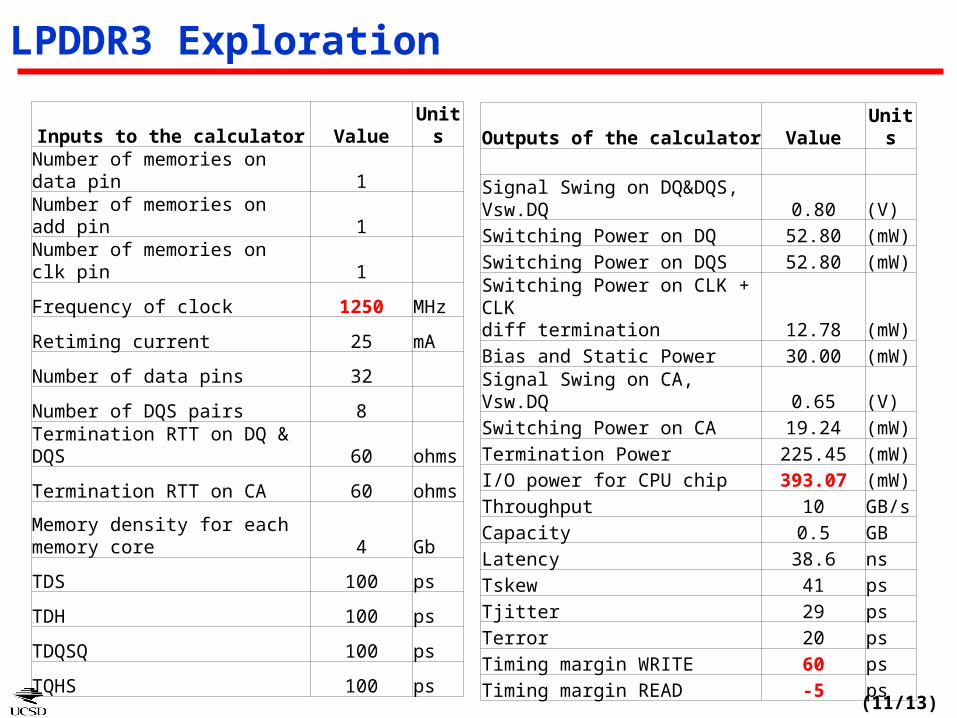
LPDDR3 Exploration
Inputs to the calculator Value Units
Number of memories on data pin 1
Number of memories on add pin 1
Number of memories on clk pin 1
Frequency of clock 1250 MHz
Retiming current 25 mA
Number of data pins 32
Number of DQS pairs 8
Termination RTT on DQ & DQS 60 ohms
Termination RTT on CA 60 ohms
Memory density for each memory core 4 Gb
TDS 100 ps
TDH 100 ps
TDQSQ 100 ps
TQHS 100 ps
Outputs of the calculator Value Units
Signal Swing on DQ&DQS, Vsw.DQ 0.80 (V)
Switching Power on DQ 52.80 (mW)
Switching Power on DQS 52.80 (mW)
Switching Power on CLK + CLK diff termination 12.78 (mW)
Bias and Static Power 30.00 (mW)
Signal Swing on CA, Vsw.DQ 0.65 (V)
Switching Power on CA 19.24 (mW)
Termination Power 225.45 (mW)
I/O power for CPU chip 393.07 (mW)
Throughput 10 GB/s
Capacity 0.5 GB
Latency 38.6 ns
Tskew 41 ps
Tjitter 29 ps
Terror 20 ps
Timing margin WRITE 60 ps
Timing margin READ -5 ps
(12/13)
LPDDR3 Exploration
Maximum speeds for: Preliminary Answers from the calculator
POP, Unterminated LPDDR3 with ~150ps memory timing parameters (tDS/tDH/tDQSQ/tQHS)?
800MHz for single-rank 800MHz for dual-rank will need careful architecture
and design
POP, Terminated LPDDR3 with ~100ps memory timing parameters? 1250MHz
External (MCP), Unterminated LPDDR3Even 533MHz for dual-rank is
challenging and may need sophisticated retiming
External (MCP), Terminated LPDDR3? 1066MHz
(13/13)
Summary and Next Steps
• A simple framework to model interconnect and IO/PHY timing and power for existing and upcoming SDRAM memory interfaces
• Helps explore standards and design space• Helps identify gaps between DRAM and SOCs• Next Steps:o Integrate the memory interface models within CACTI oChallenge the calculator for future usage cases for mobile
productso Include more parameters, including silicon area, packaging


![DWARAKA DOSS GOVERDHAN DOSS VAISHNAV …dgvcphysics.yolasite.com/resources/I M.Sc. Physics Syllabus.pdf · VAISHNAV COLLEGE (Linguistic Minority Institution) [AUTONOMOUS] ... Methods](https://static.documents.pub/doc/80x56/5abc905c7f8b9a76038e0337/dwaraka-doss-goverdhan-doss-vaishnav-msc-physics-syllabuspdfvaishnav-college.jpg)


