PRODUCT SPECIFICATION Version 0.0 12 May 2011 1 / 28 The copyright belongs to CHIMEI InnoLux. Any unauthorized use is prohibited. Customer: Common APPROVED BY SIGNATURE Name / Title Note Product Version C1/C2 Please return 1 copy for your confirmation with your signature and comments. Doc. Number : Tentative Specification Preliminary Specification Approval Specification MODEL NO.: M236HGE SUFFIX: L20 Approved By Checked By Prepared By
Transcript
PRODUCT SPECIFICATION
Version 0.0 12 May 2011 1 / 28 The
copyright belongs to CHIMEI InnoLux. Any unauthorized use is prohibited.
Customer: Common APPROVED BY SIGNATURE Name / Title Note Product Version C1/C2 Please return 1 copy for your confirmation with your signature and comments.
copyright belongs to CHIMEI InnoLux. Any unauthorized use is prohibited.
CONTENTS
1. GENERAL DESCRIPTION ......................................................................................................5 1.1 OVERVIEW........................................................................................................................5 1.2 GENERAL SPECIFICATIONS ...........................................................................................5
2. MECHANICAL SPECIFICATIONS...........................................................................................5 3. ABSOLUTE MAXIMUM RATINGS ..........................................................................................5
3.1 ABSOLUTE RATINGS OF ENVIRONMENT......................................................................5 3.2 ELECTRICAL ABSOLUTE RATINGS ................................................................................6
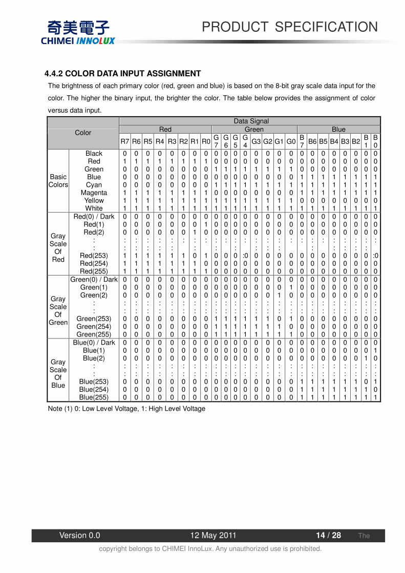
4.4 LVDS INPUT SIGNAL SPECIFICATIONS........................................................................13 4.4.1 LVDS DATA MAPPING TABLE ................................................................................. 13 4.4.2 COLOR DATA INPUT ASSIGNMENT....................................................................... 14
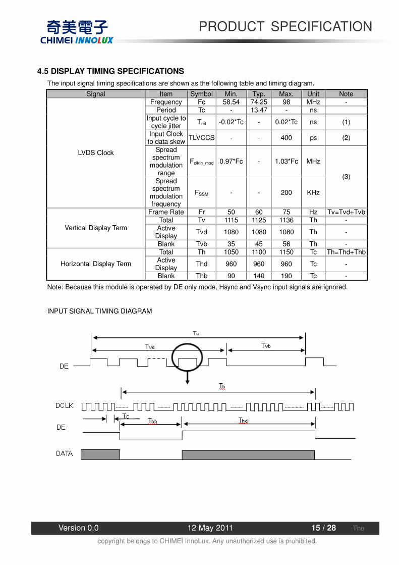
4.5 DISPLAY TIMING SPECIFICATIONS ..............................................................................15 4.6 POWER ON/OFF SEQUENCE........................................................................................17
copyright belongs to CHIMEI InnoLux. Any unauthorized use is prohibited.
REVISION HISTORY
Version Date Section Description
0.0 2011.05.05 All Tentative Specification was first issued.
PRODUCT SPECIFICATION
Version 0.0 12 May 2011 5 / 28 The
copyright belongs to CHIMEI InnoLux. Any unauthorized use is prohibited.
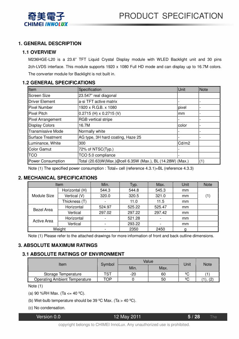
1. GENERAL DESCRIPTION
1.1 OVERVIEW M236HGE-L20 is a 23.6” TFT Liquid Crystal Display module with WLED Backlight unit and 30 pins
2ch-LVDS interface. This module supports 1920 x 1080 Full HD mode and can display up to 16.7M colors.
The converter module for Backlight is not built in.
1.2 GENERAL SPECIFICATIONS Item Specification Unit Note Screen Size 23.547” real diagonal Driver Element a-si TFT active matrix - - Pixel Number 1920 x R.G.B. x 1080 pixel - Pixel Pitch 0.2715 (H) x 0.2715 (V) mm - Pixel Arrangement RGB vertical stripe - - Display Colors 16.7M color - Transmissive Mode Normally white - - Surface Treatment AG type, 3H hard coating, Haze 25 - - Luminance, White 300 Cd/m2 Color Gamut 72% of NTSC(Typ.) - TCO TCO 5.0 compliance - Power Consumption Total (20.63)W(Max.)@cell 6.35W (Max.), BL (14.28W) (Max.) (1)
Note (1) The specified power consumption : Total= cell (reference 4.3.1)+BL (reference 4.3.3)
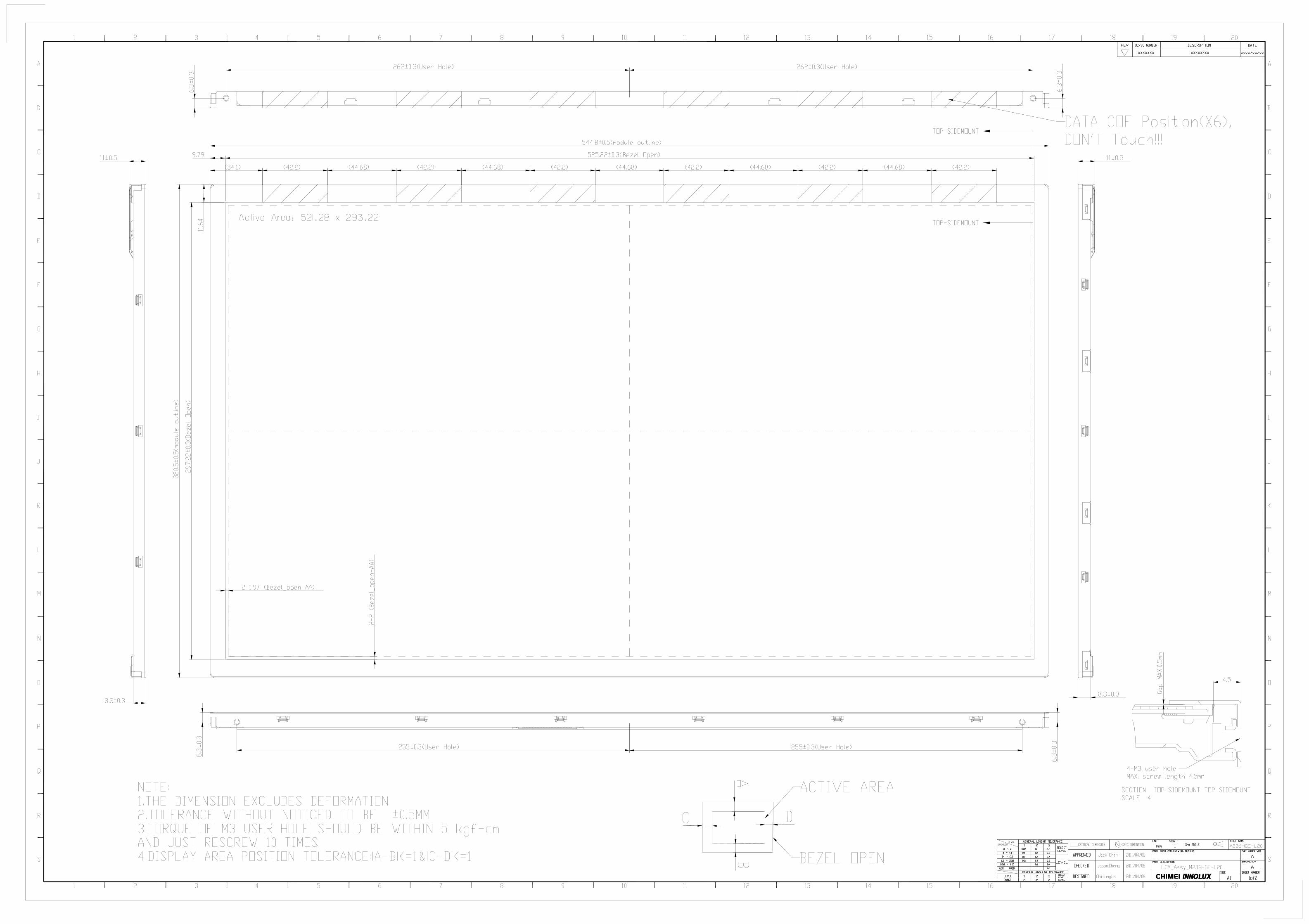
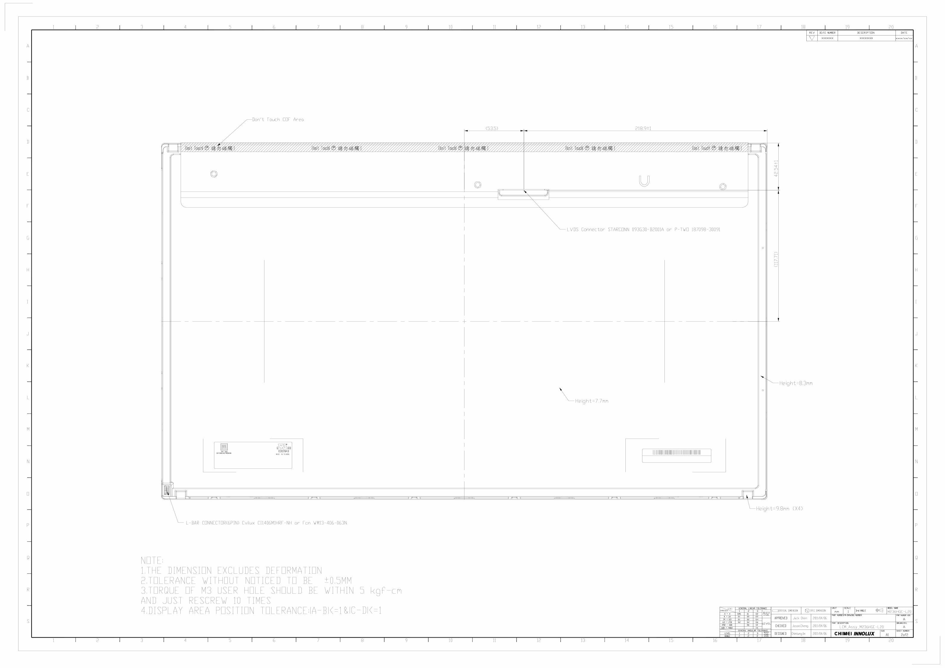
2. MECHANICAL SPECIFICATIONS Item Min. Typ. Max. Unit Note
Horizontal (H) 544.3 544.8 545.3 mm Vertical (V) 320.0 320.5 321.0 mm Module Size
Thickness (T) - 11.0 11.5 mm (1)
Horizontal 524.97 525.22 525.47 mm Bezel Area
Vertical 297.02 297.22 297.42 mm Horizontal - 521.28 - mm
Active Area Vertical - 293.22 - mm
Weight - 2350 2450 g
Note (1) Please refer to the attached drawings for more information of front and back outline dimensions.
3. ABSOLUTE MAXIMUM RATINGS
3.1 ABSOLUTE RATINGS OF ENVIRONMENT Value
Item Symbol Min. Max.
Unit Note
Storage Temperature TST -20 60 ºC (1) Operating Ambient Temperature TOP 0 50 ºC (1), (2)
Note (1)
(a) 90 %RH Max. (Ta <= 40 ºC).
(b) Wet-bulb temperature should be 39 ºC Max. (Ta > 40 ºC).
(c) No condensation.
PRODUCT SPECIFICATION
Version 0.0 12 May 2011 6 / 28 The
copyright belongs to CHIMEI InnoLux. Any unauthorized use is prohibited.
Note (2) The temperature of panel surface should be 0 ºC min. and 60 ºC max.
3.2 ELECTRICAL ABSOLUTE RATINGS
3.2.1 TFT LCD MODULE
Value Item Symbol
Min. Max.
Unit Note
Power Supply Voltage VCCS -0.3 6.0 V
Logic Input Voltage VIN -0.3 3.6 V (1)
3.2.2 BACKLIGHT UNIT Value Item Symbol
Min. Typ Max. Unit Note
LED Forward Current Per Input Pin IF 0 65 70 mA
LED Reverse Current Per Input Pin VR --- --- 85 mA
(1), (2) Duty=100%
LED Pulse Forward Current Per Input Pin IP --- --- 150 mA
(1), (2) Pulse Width10msec.
and Duty30%
Note (1) Permanent damage to the device may occur if maximum values are exceeded. Function operation
should be restricted to the conditions described under Normal Operating Conditions.
Note (2) Specified values are for input pin of LED light bar at Ta=25±2 (Refer to 4.3.3 and 4.3.4 for
further information).
PRODUCT SPECIFICATION
Version 0.0 12 May 2011 7 / 28 The
copyright belongs to CHIMEI InnoLux. Any unauthorized use is prohibited.
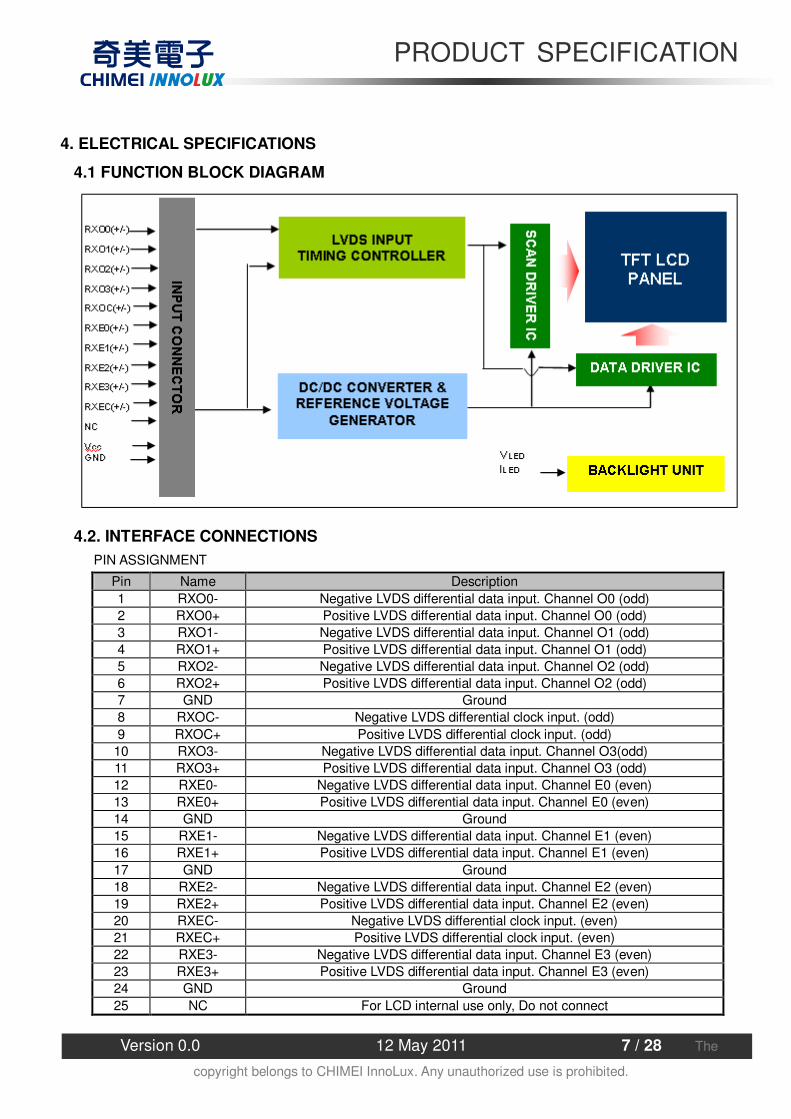
10 RXO3- Negative LVDS differential data input. Channel O3(odd) 11 RXO3+ Positive LVDS differential data input. Channel O3 (odd) 12 RXE0- Negative LVDS differential data input. Channel E0 (even) 13 RXE0+ Positive LVDS differential data input. Channel E0 (even) 14 GND Ground 15 RXE1- Negative LVDS differential data input. Channel E1 (even) 16 RXE1+ Positive LVDS differential data input. Channel E1 (even) 17 GND Ground 18 RXE2- Negative LVDS differential data input. Channel E2 (even) 19 RXE2+ Positive LVDS differential data input. Channel E2 (even) 20 RXEC- Negative LVDS differential clock input. (even) 21 RXEC+ Positive LVDS differential clock input. (even) 22 RXE3- Negative LVDS differential data input. Channel E3 (even) 23 RXE3+ Positive LVDS differential data input. Channel E3 (even) 24 GND Ground 25 NC For LCD internal use only, Do not connect
PRODUCT SPECIFICATION
Version 0.0 12 May 2011 8 / 28 The
copyright belongs to CHIMEI InnoLux. Any unauthorized use is prohibited.
Pin Name Description 26 NC For LCD internal use only, Do not connect 27 NC For LCD internal use only, Do not connect 28 Vcc +5.0V power supply 29 Vcc +5.0V power supply 30 Vcc +5.0V power supply
Note (1) Connector Part No.:
093G30-B2001A-G4(STARCONN) or 187098-30091 (P-TWO) or equivalent
Note (2) User’s connector Part No:
Mating Wire Cable Connector Part No.: FI-X30H(JAE) or FI-X30HL(JAE)
Mating FFC Cable Connector Part No.: 217007-013001 (P-TWO) or JF05X030-1 (JAE).
Note (3) The first pixel is odd.
Note (4) Input signal of even and odd clock should be the same timing.
1,1 (odd) 1,2
(even) 1,3 (odd) 1,4
(even) 2,1 2,2
3,1
Ymax,1 Ymax, Xmax
1,Xmax
Pitch
Pitch
PRODUCT SPECIFICATION
Version 0.0 12 May 2011 9 / 28 The
copyright belongs to CHIMEI InnoLux. Any unauthorized use is prohibited.
4.3 ELECTRICAL CHARACTERISTICS
4.3.1 LCD ELETRONICS SPECIFICATION Value Parameter Symbol
Min. Typ. Max. Unit Note
Power Supply Voltage Vcc 4.5 5.0 5.5 V - Ripple Voltage VRP - - 300 mV - Rush Current IRUSH - 1.52 3 A (2)
White - 0.41 0.53 A (3)a Black - 0.98 1.27 A (3)b Power Supply Current
Vertical Stripe
- 0.95 1.27 A (3)c Power Consumption PLCD - 4.9 6.35 Watt (4)
LVDS differential input voltage Vid 200 - 600 mV LVDS common input voltage Vic 1.0 1.2 1.4 V
Logic High Input Voltage VIH 2.64 - 3.6 V Logic Low Input Voltage VIL 0 - 0.66 V
Note (1) The ambient temperature is Ta = 25 ± 2 ºC.
Note (2) Measurement Conditions:
PRODUCT SPECIFICATION
Version 0.0 12 May 2011 10 / 28 The
copyright belongs to CHIMEI InnoLux. Any unauthorized use is prohibited.
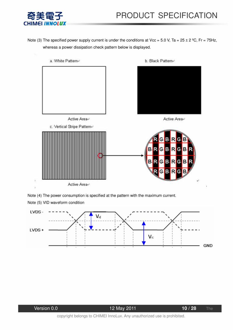
Note (3) The specified power supply current is under the conditions at Vcc = 5.0 V, Ta = 25 ± 2 ºC, Fr = 75Hz,
whereas a power dissipation check pattern below is displayed.
Note (4) The power consumption is specified at the pattern with the maximum current.
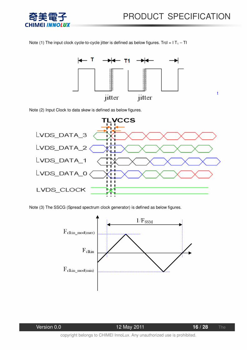
Note (5) VID waveform condition
PRODUCT SPECIFICATION
Version 0.0 12 May 2011 11 / 28 The
copyright belongs to CHIMEI InnoLux. Any unauthorized use is prohibited.
4.3.2 Vcc Power Dip Condition
4.3.3 BACKLIGHT UNIT Value Parameter Symbol
Min. Typ. Max. Unit Note
LED Light Bar Input Voltage Per Input Pin VPIN --- 46.5 51 V
(1), Duty=100%, IPIN=65mA
LED Light Bar Current Per Input Pin IPIN 0 65 70 mA (1), (2)
Duty=100% LED Life Time LLED 40000 Hrs (3)
Power Consumption PBL --- 12.09 14.28 W (1)
Duty=100%, IPIN=65mA
Note (1) LED light bar input voltage and current are measured by utilizing a true RMS multimeter as shown
below:
Note (2) PBL = IPIN × VPIN × ( 4 ) input pins.
Note (3) The lifetime of LED is defined as the time when LED packages continue to operate under the
conditions at Ta = 25 ±2 and I= (25)mA (per chip) until the brightness becomes 50% of its
original value.
msTdVVccV 20,5.40.4 ≤≤≤
PRODUCT SPECIFICATION
Version 0.0 12 May 2011 12 / 28 The
copyright belongs to CHIMEI InnoLux. Any unauthorized use is prohibited.