142 IEEE TRANSACTIONS ON INDUSTRIAL ELECTRONICS AND CONTROL INSTRUMENTATION, VOL. IECI-26, NO. 3, AUGUST 1979 Modeling of Switching Regulator Power Stages With and Without Zero-Inductor-Current Dwell Time FRED C. Y. LEE, MEMBER, IEEE, AND YUAN YU Abstract-State-space techniques are employed to derive accurate models for the three basic switching converter power stages: buck, boost, and buck/boost operating with and without zero-inductor- cufrent dwell time. A generalized procedure is developed which treats the continuous-inductor-current mode without dwell time as a special case of the discontinuous-current mode when the dwell time vanishes. Abrupt changes of system behavior including a reduction of the system order when the dwell time appears are shown both analytically and experimentally. Merits resulting from the present modeling technique in comparison with existing modeling techniques are illustrated. I. INTRODUCTION M sODELING and analysis of switched dc-dc converter power stages, such as buck, boost, and buck/boost converter shown in Fig. 1, has been achieved through averaging approaches [1]- [5] . The operation of such converters can be represented by a cyclic change of two power-stage topologies within each switching cycle; one for the on-time interval while the other for the off-time interval of the power switch. How- ever, either by design intent or through fight-load operation, a steady-state cycle invariably contains an interval during which the inductor MMF vanishes, as shown in Fig. 2(b). This inter- val begins when the descending MMF reaches zero during the off time of the power switch, and ends when the power switch is turned on to initiate the next on-time interval. During this zero-inductor-current dwell time, the topology of the power stage consists only of the filter capacitor and the load, which is different from both the on-time interval of ascending MMF and the off-time interval of descending MMF. The addition of such a dwell time considerably complicates the afore- referenced analytical approaches [4] . Projoux et al. [6], [7] have presented an approach capable of describing accurately certain nonlinear system under periodical structural changes by a linearized discrete time- domain model, and have applied such a technique to a boost converter operating with zero-inductor-current dwell time. The present paper extends the analysis to all three types of converters: buck, boost, and buck/boost, operating with and without such a dwell time. The duty-cycle-to-output-voltage discrete time-domain models are derived in closed forms, Manuscript received June 14, 1978; revised April 15, 1979. This work was performed under NASA Contract NAS3-1 960, "Modeling and Analysis of Power Processing Systems," by TRW Defense and Space Systems, Redondo Beach, CA, for NASA Lewis Research Center. F. C. Y. Lee is with the Department of Electrical Engineering, Vir- ginia Polytechnic Institute and State University, Blacksburg, VA 24061. Y. Yu is with the TRW Defense and Space Systems, Power Processing and Control Department, Redondo Beach, CA 90278. Yj - HO TIME CONTROL DUTY CYCLE FEEDBACK I CONTROL Q _AMPLIFIER Fig. 1. DC-dc energy storage converter with three basic power stage configurations. INDUCTOR MF _ _ TON TF FPOWER POWER SWITCH OFF, SWITCH DN. DIODE ON DIODE OFF (a) TON TFI TF2 POWER POWER SWITCH OFF, SWITCH ON, DIODE OFF DIODE ON DIODE OFF (b) Fig. 2. (a) Continuous and (b) discontinuous inductor current MMF. which describe converters about their equilibrium state exactly up to one half of the switching frequency. A generalized procedure is developed in this paper which not only avoids laborious derivations for each converter but also treats the continuous current mode without the dwell time as a special case of the discontinuous current mode when the dwell time vanishes. The mathematical models derived from this unified approach are compared with the currently used average model the ac- curacy of which is known to be limited to low modulation 00 18-9421/79/0800-0142$00.75 1979 IEEE BUCK | 'L I wi > o§o- t00 I t BOOST - r 1 C BUCK/B0OS N i R C -PJR d )
Transcript
142 IEEE TRANSACTIONS ON INDUSTRIAL ELECTRONICS AND CONTROL INSTRUMENTATION, VOL. IECI-26, NO. 3, AUGUST 1979
Modeling of Switching Regulator Power StagesWith and Without Zero-Inductor-Current
Dwell Time
FRED C. Y. LEE, MEMBER, IEEE, AND YUAN YU
Abstract-State-space techniques are employed to derive accuratemodels for the three basic switching converter power stages: buck,boost, and buck/boost operating with and without zero-inductor-cufrent dwell time. A generalized procedure is developed which treatsthe continuous-inductor-current mode without dwell time as a specialcase of the discontinuous-current mode when the dwell time vanishes.Abrupt changes of system behavior including a reduction of the systemorder when the dwell time appears are shown both analytically andexperimentally. Merits resulting from the present modeling techniquein comparison with existing modeling techniques are illustrated.
I. INTRODUCTIONMsODELING and analysis of switched dc-dc converter
power stages, such as buck, boost, and buck/boostconverter shown in Fig. 1, has been achieved through averagingapproaches [1]- [5] . The operation of such converters can berepresented by a cyclic change of two power-stage topologieswithin each switching cycle; one for the on-time interval whilethe other for the off-time interval of the power switch. How-ever, either by design intent or throughfight-load operation, asteady-state cycle invariably contains an interval during whichthe inductor MMF vanishes, as shown in Fig. 2(b). This inter-val begins when the descending MMF reaches zero during theoff time of the power switch, and ends when the power switchis turned on to initiate the next on-time interval. During thiszero-inductor-current dwell time, the topology of the powerstage consists only of the filter capacitor and the load, whichis different from both the on-time interval of ascending MMFand the off-time interval of descending MMF. The additionof such a dwell time considerably complicates the afore-referenced analytical approaches [4] .
Projoux et al. [6], [7] have presented an approach capableof describing accurately certain nonlinear system underperiodical structural changes by a linearized discrete time-domain model, and have applied such a technique to a boostconverter operating with zero-inductor-current dwell time.The present paper extends the analysis to all three types ofconverters: buck, boost, and buck/boost, operating with andwithout such a dwell time. The duty-cycle-to-output-voltagediscrete time-domain models are derived in closed forms,
Manuscript received June 14, 1978; revised April 15, 1979. Thiswork was performed under NASA Contract NAS3-1 960, "Modeling andAnalysis of Power Processing Systems," by TRW Defense and SpaceSystems, Redondo Beach, CA, for NASA Lewis Research Center.
F. C. Y. Lee is with the Department of Electrical Engineering, Vir-ginia Polytechnic Institute and State University, Blacksburg, VA 24061.Y. Yu is with the TRW Defense and Space Systems, Power Processing
and Control Department, Redondo Beach, CA 90278.
Yj-HO
TIME CONTROL
DUTY CYCLE FEEDBACK ICONTROL Q _AMPLIFIER
Fig. 1. DC-dc energy storage converter with three basic power stageconfigurations.
INDUCTORMF _ _
TON TF
FPOWER POWER SWITCH OFF,SWITCH DN. DIODE ONDIODE OFF
(a)
TON TFI TF2
POWER POWER SWITCH OFF,SWITCH ON,DIODE OFF DIODE ON DIODE OFF
(b)
Fig. 2. (a) Continuous and (b) discontinuous inductor current MMF.
which describe converters about their equilibrium state exactlyup to one half of the switching frequency. A generalizedprocedure is developed in this paper which not only avoidslaborious derivations for each converter but also treats thecontinuous current mode without the dwell time as a specialcase of the discontinuous current mode when the dwell timevanishes.The mathematical models derived from this unified approach
are compared with the currently used average model the ac-curacy of which is known to be limited to low modulation
0018-9421/79/0800-0142$00.75 1979 IEEE
BUCK | 'L I
wi > o§o-t00 ItBOOST -r 1 C
BUCK/B0OS N i RC-PJRd )
LEE AND YU: SWITCHING REGULATOR POWER STAGES AND DWELL TIME
frequency. The improvement of converter models employingthe discrete time modeling technique is illustrated. The con-verter models developed in the present paper are also em-ployed to investigate certain observed anomalies of switchingregulator performances in the transition between continuousand discontinuous inductor current operations. Certainabrupt changes often can be observed in the breadboardperformance when the inductor current leaves the continuousmode and enters into the discontinuous mode. For example,step transient response may change from oscillatory to welldamped, and the audio signal rejection capability is generally im-proved. More significantly, the stability nature of the systemcan be changed from an unstable system to a stable one. Suchimportant phenomena, which intimately affect converter de-sign philosophies, are investigated for the first time.
II. DEVELOPMENT OF POWER STAGE MODELS-AGENERAL PROCEDURE
Consider the small-signal behavior of the converter about itsequilibrium state that is linear. When the converter is sub-jected to a small disturbance, the duty-cycle signal d(t) is modi-fied as d(t) + Ad(t), shown as Fig. 3. Such a perturbed duty-cycle signal can be idealized as an impulse train when theperturbation is vanishing slowly. A linearized discrete im-pulse response which characterizes the small-signal behaviorof the power stage about its equilibrium state can be obtainedif the perturbation of the output voltage, subjected to a smallduty-cycle disturbance at the kth switching cycle can be com-puted after n cycles of propagation. This concept can beelaborated by Fig. 4 and the following equation:
AVo(tk+n) A g(nT ) (1)Atk
where Atk is a small duty-cycle disturbance at the kth switch-ing cycle and A Vo(tk+ n) is the resulting output voltage varia-tion at the (k + n)th cycle. The sampling rate is equal to theswitching frequency I/Tp. Through mathematical manipula-tion, the discrete impulse response g(nTp) can be expressedin the closed form as a function of nTp, the power stageparameters, and the steady-state operating conditions. Forconvenience, the converter operations with and withoutzero-inductor-current dwell time are referred to in the textas "Mode 2 operation" and"Mode 1 operation," respectively.
A. State-Space RepresentationsThe switching regulator power stage, during one cycle of
operation, can be represented by three piecewise-linear vectordifferential equations
X = F1 X + G1 U during TF1 (2)
d ( t ) m > d ( t)+d d(t)
(a)VnI
TON TFl+TF2 -
Ad(t) J i
(b) F'Fig. 3. (a) The duty-cycle signal at steady state d(t), and after smallperturbation d(t) + Ad(t). (b) The perturbed duty cycle Ad(t).
Fig. 5. State trajectories for steady state (solid line) and perturbedstate (dotted line).
B. Linearized Discrete Impulse ResponseConsider the following duty cycle signal:
){1,1 during TOd=0' otherwise
whose leading edge of TON is always initiated by a clock sig-nal. When the converter is subjected to a small duty-cycledisturbance, the propagation of the perturbed state can beillustrated in Fig. 5. The steady state with a superscript ""'
is shown as the solid curve, while the perturbed state witha superscript "*" is represented by the dotted curve. For asmall duty-cycle perturbation at kth cycle from t4 to tq, theperturbed state after one cycle of propagation is expressed asX*(t44l). The trajectories for the perturbed state duringeach piecewise4inear region can be represented by the fol-lowing state transition equations (5)(7) which are the solu-tions for the vector differential equations (2)44).
X*(4s)1(ts- tZ) X*(tZ)
X=F2X+G2U duringTF2X=F3X+G3U duringTON
(3)
(4)
tki
tk4)1(-s) dsGlU (5)
where U= Vs.The time intervals TF1, TF2, and TON are defined in Fig. 2.
It should be noted that, for Mode 1 operation, the time inter-val TF2 does not exist. Therefore, the vector differentialequation (3) can be neglected.
X *(tk2) = (2(tk2- tZ)X*(tt1)
+ 4)2 (t2 ) ftk 2 (-s) dsG2Ut1
(6)
143
t
t
144 IEEE TRANSACTIONS ON INDUSTRIAL ELECTRONICS AND CONTROL INSTRUMENTATION, VOL. IECI-26, NO. 3, AUGUST 1979
X*(to +1 ) = 13(t41X tkZ2) X*(tkZ2)
r+o+43(tZo1) 4k43(-s)dsG3U (7)
k2
where 4's are the state transition matrices defined as
Fi(T) eFiT i = 1, 2, 3.
Since the clock signal initiates the turn-on time, the timeinstant t*2 is equal to 4k2 in (7).The corresponding discrete impulse response for each
switching power stage represented by (1) can be obtainedby performing the following vector differentiation:
g(nT ) = CdX*(rr+) (8)dtZ
Since the output voltage of the converter can be expressed asV0 = CX, where C is a constant row matrix. Applying chainrule, one can express (8) by the following recurrence relation:
dX*(t4 v I) dX*(to+) dX*( d tZ1)dX*(tZ) dX*(4k2) dX*(41s2) dX*(t)'
for Mode 2 operation (10)
_ dX*(t%dX*(tX (tZ1)dX*(4k2) dX*(T)
for Mode 2operation. (11)It is proved in the Appendix for all three converters that
dX*(t+ 1) FP(Tp) = F3(T;N) 42(T;2)dX*(tk[)
= lb3(T;N) 4l (7$), Mode 1 (13)
and
dX(4) B = (F3 - Fl) Xr(t4) + (G3 - G1) U (14)dtt
where X0(t') is the state at the instant of sampling and is de-fined as [IM VcI for buck and boost converters and 1 CMV]Tfor buck/boost converter. It should be noted that, for boostand buck/boost converters, the output voltage V0 has a jumpat the instant of sampling, since the current through the ESRRc of the output filter capacitor is discontinuous at thesampling instant. Therefore, the sampling instants need to becarefully defmed. In the present analysis, the samples are
selected after the jump, Vo(t) = Vo(t+), such that the effectof ESR to the jump is included in the model.
Substituting (1 2)-(14) into (9), one can obtain
dX*(4+n) = cnF(Tp)B.dt*
(15)
The state transition matrices, (D (T;1 ), F2 (Tn2), and 4K3 (TON)are presented in Table II. The derivations for these state tran-sition matrices are straightforward and are neglected in thetext. The explicit representations for 4F(p) and 'F(Tp)associated with each converter are given in Section III.The linearized discrete impulse response is obtained by
substituting (15) into (8)
g(nTp) = CFn(Tp) B (16)
C. Continuous Models-Time Domain andFrequency Domain
The linearized discrete impulse response g(nTp) developed inthe previous section characterizes the small-signal behavior ofthe converter exactly but only at discrete sampling instant. Ifone is willing to neglect the detail waveforms between samplesand study the long-range trend of the converter, an equivalentcontinuous linear impulse response g(t) can be obtainedsimply by substituting t = nTp into the expression for g(nTp).It is important to note that the discrete-to-continuous trans-formation is meaningful only if the system response is muchslower than the sampling rate. Otherwise, a significant phasedelay can be introduced. Such a transformation is madeplausible, in the present analysis, by the fact that every con-verter power stage inherently has a low-pass LC filter whichlargely attenuates the high-frequency switching ripple; thenatural resonant frequency of the output filter is usuallydesigned to be 1/15 to 1/20 of the switching frequency toachieve good output voltage regulation. The continuous linearimpulse response g(t) so derived represents small-signal low-frequency characteristics of the converter up to one-half ofthe switching frequency.
III. EXAMPLES
The aforedescribed modeling technique is employed toderive small-signal continuous models for the three basicconverter power stages; buck, boost, and buck/boost withMode I and Mode 2 operation. The F's and G's matrices foreach converter are presented in Table I. The inductor currentand the capacitor voltage, X = [UL Vc] T are chosen as twostate variables for buck and boost converters. For the buck/boost converter, however, the current through either theprimary winding or the secondary winding of the inductor isnot continuous. The magnetic flux 4 instead of inductorcurrent is chosen as one state variable.
TIhe state transition matrices F1l (TFI), 42(TF2) and43(TON) are presented in Table II. Matrices (F(Tp) for buck,boost, and buck/boost converters in both Mode 1 and Mode 2operations can be computed in a straightforward manner using(12), (13) and Table II. The results are presented in Table III.The linearized discrete impulse response g(nTp) as shown in
(16) is evaluated for each converter in the following.
LEE AND YU: SWITCHING REGULATOR POWER STAGES AND DWELL TIME
TABLE ISTATE VARIABLES AND SYSTEM EQUATIONS
-- -r-1 1 I r I
F~~~F = L f 2fn o G][O[RCL LR R 1R RR R F IFolCL L i C L L 0_BUCK L(RC+RL) °tRC+RL) 0 0 OL(Rc4L LIRCiRIJJT
RL R110 -1 -1C(RC+RLC(RCeL)i L CIRC+RL C(RC+RL C(RC+RL oj0
[ RCRL AL 1 0 CRiL]1l 1 1 0
L CIRC+RL) C(Rt 0 --C ) Li UR . LiBUCK F -t CL ~~~RL iF0 01 [
BOOST~~~~.A~REL .nR~L . _R Where a
BUCK -x C L L1 0 -l 0
LANXsRI+RJ (R+L) L C(RCtRL) IR LLT 0 L0Where -magnetic permeability; t *mean length path A =cross section area
TABLE IISTATE TRANSITION MATRICES CORRESPONDING TO THE THREE TIME
INTERVALS: TON, 7I,I AND T
F2
A. Buck Converter
1) Mode 2 Operation: Referring to Table III, it is easy toprove that
01 1022 - 012 021 =0. (17)
One can express
(5(Tp)]=2=eOTP( i1I + 022) 4(Tp). (18)The following result is obtained by mathematical induction:
g(nTp) = C0(nTp)B. (23)B. Boost Converter1) Mode 2 Operation: It is shown in Table III that the
expression 4(Tp) for the boost converter is a special case ofbuck converter where 1 1 = 0P12 = 0. Therefore, it is straight-forward to show that
q.f(Tpj = eiafTP022n1 [0 952021 022
and
g(nT)=C (B 021 B2) eF-a+/TpblnP22nTp~'2k" 022
(24)
(25)
II
145
F1 Ff7 f22l GI G2 G3F3
146 IEEE TRANSACTIONS ON INDUSTRIAL ELECTRONICS AND CONTROL INSTRUMENTATION, VOL. IECI-26, NO. 3, AUGUST 1979
TABLE IIILINEARIZED STATE TRANSITION MATRICES
Applying Table I one can express
St4
0
MODE 2
t(T ) A e aTp 21 j12T
L21 ~22ja -f + (f +Oi)(T(N+T )lT22 22i ONi
f f211 = 12 21 sintT anuT11 2 dnTONsnTFlf12 Od-f2212 = si2wT (~~~?~ws inuT +coswTto ON to El Fl'
221 = --inuoT +cosw cT)21into ON ONT~noF222- (--??-smnu3T ±CosTto ON OTN)
(-sinwTFl+cosw,T )l
MODE 1
-aT12(TY e- aTpp 21
a = a
¢II =Cf
11 inwT +cosuTw p p
12 = 2inwTw p
21 = -- inwTw p
222 = 22osnwT +coswTw p p
a -f22+(f22+cTFl Tp aa-'T I/Ts }121 _ cc I
i Tf 12 _ 1p
212 = 0 5 osinw'T1Fl+cos?j1f2 1o 21= -sinT 12 Fo to ~~~FlU'= F
P f
2 2 T 21 =- 2inwT22 t Siw Fl+csTFl WT Fl
g Same as boost converter Same as Boost Converter
Fwhere D' = T '/T, c'= (-f11-f22/D')/2, =f1=f22/D -(f11+f22 D')
where
B = [VO _ RL I]T (26)B C(RC + RL) IM] (2)
C= [R§VtL RC+LY (27)
The inductor current and the output voltage at the samplinginstant t4 can be expressed in terms of known circuit param-eters and the input voltage
1(8IM = -TON V1 (28)L
V (1+ TO) V (29)
2) Mode ] Operation: By definition
'J (T ) e F3TONe FT (30)
Applying the Baker-Campbell-Hausdorff series [101, whichsays
eAeB= ec
where
C = A + B + 4 (AB - BA) + higher order terms.
(31)
(32)
Employing the first two terms of (32), one can approximateby
eFTp ef3TON + (Fl TFp )(F3TON)(F1TFl)
-(F1TFI )(F3TON) (33)
[DI FTp =
f2 lD (1+ f22 TON)fl2D'(1 - f22 TON)1
f22
Since the following inequality is always true:
If2TN =~~ TON _<C(RC+RL)
(34) can be simplified by
[f ID' f 2D'1
Therefore,
n(Tp) = eFnTp = 'F(nT )and
(34)
(35)
(36)
(37)g(nTp) = C4(nTp)B.The matrices B and C are represented by (26) and (27), butwith the following modifications
I IV -DT,,VIMD'2RL ' 2L
VD==IID'
(38)
(39)
where
D- TONI/TP D- TFI/TP.
C. Buck/Boost ConverterThe mathematical expression for the discrete impulse re-
sponse for the buck/boost converter is exactly the same as theboost converter for both mode 1 and mode 2 operations,except C and B are defined as
~=C= (- c RLtANSRC+RRL Rc+R+ LJ
B[VN +V -l RCRL Oms[N7+7 ANsRC+R
and
1Om =N-TONVI' Mode 2
I DL L I-------VI+ ~DTpVINp DY2 RL 2Np
(40)
(41)
Mode 1
=Ns TONVVNp TF1 Mode2
N.D= bT Model.Np
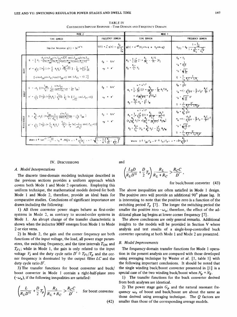
The continuous impulse response functions g(t) and theircorresponding frequency domain transfer functions G(s) arepresented in Table IV for both Mode 2 and Mode 1 operations.
LEE AND YU: SWITCHING REGULATOR POWER STAGES AND DWELL TIME
TABLE IVCONTINUOUS IMPULSE RESPONSE --TIME DOMAIN AND FREQUENCY DOMAIN
MODE 2 MODE 1
TIME DOMAIN FREQUENCY DOMAIN TIME DOMAIN FREQUENCY DOMAIN
Impulse Response g(t) Gea t GS=g -§t) et'Klnwt+ 'K2t05 t| G(s) Gp 1
V -RcsinwToNsinTF]+tvtC cos(wTON-o)sinwTFl 1 2 RC RC2CG L I sinwTONsinwTFl+cos(wT5 O)cos(wTFl-O Gp = G/a' |r [1+T 17 - ]VI(4 = 1
Wa R-1 TON+T~F£1 Y
c' 7'C [+ri (-1+ C In LCa 2 L IL2-I p Tp a 2=---o
[-sinwT0 NsinuT +cos(TON-s) cos (wT1|
TON sinwTFl |y G = G/a' RC 4-)
G Y' V [l+(-+T-)c L ]- -Tp ln[ ON (-Tl- p 2l2+ YLr D R1 C
NpVI[ (l - cos(.T,1oT KR CON]-§YU|r-FC~~~~~~~~~~~~~~~~~~~~~~~~~G 1~~ ~ + W6 rLa c 1 ap = aL C a =o((- LD T r0
C> T~~~~ TL
a,G -yV1 Ci FOTcos£LCTN +4K (RrL%U1 +71.fr..a-.-
I t-RRL -F 1-I Ca --IT al
a LC= [ 2- +- RCR)Tp ]- 'n- Na 2
2 Ve P L M 2
22T sin2 L2-11RR2 ' - R-_ _O 1 F T_ GCGa
G I - I~~~~L L 4_ 7a~raDUrD /TP.D/T.P
IV. DiSCUSSIONS
A. Model Interpretations
The discrete time-domain modeling technique described in
the previous sections provides a uniform approach which
covers both Mode I and Mode 2 operations. Employing this
uniform technique, the mathematical models derived for both
Mode and Mode 2, therefore, provide an ideal basis for
comparative studies. Conclusions of significant importance are
drawn including the following:1) All three converter power stages behave as first-order
systems in Mode 2, as contrary to second-order systems in
Mode 1. An abrupt change of the transfer characteristic is
shown when the inductor MMF emerges from Mode I to Mode
2 or vice versa.
2) In Mode 2, the gain and the corner frequency are both
functions of the input voltage, the load, all power stage param-
eters, the switching frequency, and the time intervals TON and
TF1; while in Mode 1, the gain is only related to the input
voltage VI and the duty cycle ratio D'8
TF/Tp and the cor-
ner frequency is dominated by the output filter LC and the
duty cycle ratio D'.3) The transfer functions for boost converter and buck/
boost converter in Mode contain a right-half-plane zero
(w,), if the followinginequalities are satisfied:
L+_ R RL R- CL2 +4 TP > for boost converter
LD' 2 "/RL +RC D'
and
LsD D \ RL RCC_2FT e >- 1(RLD 2 P RL +RC D
for buck/boost converter (43)
The above inequalities are often satisfied in Mode 1 design.The positive zero wifl provide an additional 900 phase lag. Itis interesting to note that the positive zero is a function of theswitching period Tp [7]. The longer the switching period thesmaller the positive zero -wco; therefore, the effect of the ad-ditional phase lag begins at lower corner frequency [7].The above conclusions are only general remarks. Additional
insights to the models will be provided in Section V whereanalysis and test results of a single-loop-controlled buckconverter operating at both Mode I and Mode 2 are presented.
B. Model ImprovementsThe frequency-domain transfer functions for Mode1 opera-
tion in the present analysis are compared with those developedusing averaging technique by Wester etal. [1, table 1] withthe following important conclusions. It should be noted thatthe single winding buck/boost converter presented in [1] is aspecial case of the two winding buck/boost whenNp = Ns.
1) The transfer functions for the buck converter derivedfrom both analyses are identical.2) The power stage gainGp and the natural resonant fre-
quencywo of boost and buck/boost are about the same asthose derived using averaging technique. The Q factors aresmaller than those of the corresponding average models.
147
148 IEEE TRANSACTIONS ON INDUSTRIAL ELECTRONICS AND CONTROL INSTRUMENTATION, VOL. IECI-26, NO. 3, AUGUST 1979
Fig. 6. Frequency response for the boost converter power stage fromthe present analysis (solid curves) and the average model (dottedcurves).
V. VERIFICATIONSA buck converter, represented by the block diagram in Fig.
1, was designed to operate in the continuous-current modelunder normal-to-heavy load conditions and in the discontin-uous-current mode at light load. The small-signal block dia-gram of the converter is shown as Fig. 7. The compensationnetwork is a lead-lag circuit having the following knowntransfer characteristic:
G = 193.3 1 +f/20 1 + ff1225c 1 1 f/.3 1 +f/3263(
The pulsewidth modulator, as shown in Fig. 8, compares theerror signal Ve (t) with a fixed ramp A (t).
A (t) = Ao(t - nTp), nTp < t < (n + 1) Tp (46)3) The transfer functions for boost and buck/boost have
one positive zero and one negative zero in average models butonly has one conditional positive zero in the present models.4) The positive zero for boost and buck/boost converters is
a function of the switching frequency, while its counterpartis independent of the switching frequency.For convenience, the transfer function of the boost con-
verter derived from averaging technique is presented in thefollowing:
G(s) = Gp 1C° a (44)I s--- -2Q Wo W2
where
1/ t \~~-1 Dt2Rt 1Ql1 RC+ L Da= RL-C~cJO RLDI2 0 L ZCR
I D'2LLCRL+RC
For comparison, the gain and phase plots of a boost con-verter derived from both the averaging technique and the presentanalysis are sketched in Fig. 6. The following numerical valuesare used: Tp = 10-4 s, L _6 mH, C = 41.7giF,RL= 60 Q,RC = 1 a, VI = 60 V, V0 = 30 V. Excellent agreements areshown between results of these two analytical approaches inthe low-frequency range, except a higher resonant peak isshown in the average model [3]. The differences of these twomodels become significant when the frequency is greater thanI kHz, the average model has larger gain and phase angle. Thisis primarily due to the somewhat different effects of thecapacitor ESR as results of the two different modeling tech-niques. Comparing (19) with the corresponding transfer func-tion in Table IV, a stronger contribution of ESR to the phaselead is shown in the average model due to the additionalsecond-order term -S2/(caoWz), in the numerator. This mayvery well explain the reported discrepancy between averagingmodels and measurement data at high frequency. The measure-ment data show a lesser gain and a smaller phase angle begin-ning at about 1/10 of the switching frequency.
where Ao = 6.25 X 10⁴ V/s is the slope of the ramp. Theoutput of the PWM is a unity pulse train, with its pulseduration governed by (47)
d (t) 2{1I
ifA (t) < Ve (t)O0t ifA (t) > Ve (t)
(47)
The describing function of the PWM was derived in [2] ; thegain ofPWM is simply
kM = 1/Vp. (48)Due to the circuit implementation, there is an 8-,us delay
from the signal d(t) to the power switch. For convenience,this time delay is included in the PWM functional block inFig. 7. The transfer function of the PWM is represented as
GM = (I/AoTp)eJIWd (49)
The circuit parameters used for the power stage are listed:Ll=ImH,C= 455g F,Rc=0.034Q,RL=l150Q, Tp =50ps,VI=40V,and V, = 20V.Fig. 9 shows the frequency response of the power stage
together with the PWM in Mode 2 operation. Measurementresults confirm the analytical findings that the order of thesystem is reduced for Mode 2 operation. For comparison, theanalytical gain and phase ofGMG for Mode 1, when RL = 6.67Q, is also presented in Fig. 9 as dotted-line curves. It is evi-dent that the converter behaves as a first-order system in Mode2 in contrast to a second-order system in Mode 1. In Mode 2,since the phase lag of GMG is at most 90° and the corner fre-quency is usually low, only a gain compensation (an erroramplifier) is needed to improve the transient response and toensure the loop stability.
It has been made evident in the analysis that an abruptreduction of system order (a jump phenomenon) is shownwhen the inductor MMF emerges from Mode I to Mode 2 orvise versa. This was verified by measuring the open-loopcrossover frequency of the converter when the load is grad-ually reduced. The crossover frequency, as shown in Table V,remains unchanged as long as the converter is operating inMode 1. When the load is reduced to approximately 90 to 100Q, the converter begins to operate in between Mode 1 andMode 2 affected by the disturbance of the small injected sig-
(45)
LEE AND YU: SWITCHING REGULATOR POWER STAGES AND DWELL TIME
ER -
Fig. 7. Simplified block diagram for a buck converte
PWM
d(t)
Le t)
At) IeG
TON TI$ T + TON 21P
Fig. 8. Waveforms for the pulsewidth modulator.
Fig. 9. Frequency response for buck converter power stage togetherwith PWM in mode 2 (solid curves) when RL = 150 a, and Mode 1(dotted curves) when RL = 6.67 Q2.
TABLE VOPEN-LOOP CROSSOVER FREQUENCY AS A FUNCTION OF LOAD
nals for measurement purposes. A very significant reductionof the crossover frequency can be seen when the load islighter than 110 t2. Further increasing RL only results in agradual reduction of the crossover frequency.The previous discussions reveal certain unique performance
characteristics associated with Mode 2 operation, which verymuch affect the basic design philosophies. For example, theloop stability becomes a trivial problem and the transientresponse is well damped rather than oscillotory.
VI. CONCLUSIONSState-space techniques are employed to derive discrete
models for buck, boost, and buck/boost converters operatingwith and without zero-inductor MMF dwell time. The duty-cycle-to-output linear discrete-time-domain models are derivedin closed forms, which describe the discrete behavior of con-
verters about their equilibrium state exactly. These discrete
models are then approximated by frequency-domain transferfunctions representing the low-frequency characteristics ofconverters up to one-half of the switching frequency.The power stage models are shown to be first order for all
three converters with the dwell time, as opposed to secondorder without the dwell time. The analysis makes evidentcertain abrupt changes of system behavior often observed inthe breadboard performance when the dwell time appears.These include pronounced improvements of stability margin,and transient response, from oscillatory to well damped.
(t) Graphs are presented to illustrate influences of power stageparameters, switching frequency, input voltage, load, and thetime intervals corresponding to the ON and OFF of the power
(t) switch to a buck converter with the dwell time. Foundation islaid for power stage design and tradeoff evaluation for con-verter operating with and without zero-inductor-current dwelltime.Evaluations of converter performance are also made between
the present models and the corresponding average models..-r Certain improvements of the present models are shown in the
high-frequency range when the output-filter capacitor ESR-60° begins to shape the gain and phase of their correspondingfrequency responses.The general modeling and analysis technique presented in
--,2 the paper can be applied to many other switching convertertypes which share the common property of periodical varying
15W the circuit topology and invariably operate in both the con-tinuous and discontinuous inductor current mode dependingupon various line and load conditions.
IOOK APPENDIXA. Derivations for [dX*(tO+I )] /dX*(t%)Applying the Chain Rule, one can express
For small-signal disturbances, the following expression can besimplified, for all converters:
[1] G. W. Wester and R. D. Middlebrook, "Low-frequency character-ization of switched dc-dc converters," IEEE Pans. Aerosp.Electron. Syst., voL AES-9, pp. 376-385, May 1973.
[21 G. W. Wester, "Linearized stability analysis and design of a fly-back dc-dc boost converter," inIEEE Power Electronics SpecialistsConf: Rec., pp. 130-137, June 1973.
[3] R. D. Middlebrook, "Continuous model for the tapped-inductorboost converter," in IEEE Power Electronics Specialists Conf:Rec., pp. 63-79, June 1975.
[4] R. D. Middlebrook and S. Cuk, "A general unifled approach tomodeling switching-converter power stages," in IEEE PowerElectronics Specialists Confi Rec., pp. 18-34, 1976.
[5] S. Cuk and R. D. Middlebrook, "A general unified approach tomodeling switching dc-to-dc converters in discontinuous conduc-lion mode," in IEEE Power Electronics Specialists Confi Rec.,1977.
[6] R. Prajoux, J. C. Marpinard, and J. Jalade, "Accurate mathemat-ical modeling of PWM power regulators," NASA Tech. Transla-tion, NASA TTF-15947, Sept. 1974.
[7] A. Capel, J. G. Ferrante, and R. Pajoux, "State variable stabilityanalysis of multi-loop PWM controlled dc/dc regulators in lightand heavy mode," in IEEE Power Electronics Specialists Conf.Rec., pp. 91-103, June 1975.
[81 B. C. Kuo, Analysis and Synthesis of Sampled-Data ControlSystems. Englewood Cliffs, NJ: Prentice-Hall, ch. 4.
[9] D. Y. Chen, H. A. Owen, Jr., and T. G. Wilson, "Computer-aided design and graphics applied to the study of inductor-energy-storage dc-to-dc electronic power converters," IEEE Trans.Aerosp. Electron. Syst., vol. AES-9, pp. 585-597, July 1973.
[101 R. Bellman, Perturbation Techniques in Mathematics, Physics andEngineering. New York: Holt, Rinehart and Winston, pp. 38-39.