15
1 Modeling of total dose radiation effect of RF PD SOI-MOSFET using Sentaurus TCAD Krasukov A.Y. Mansurov A.N. Shlikova K.A. Griaznov E.G.

1
Modeling of total dose radiation effect of RF PD SOI-MOSFET
using Sentaurus TCAD
Krasukov A.Y. Mansurov A.N. Shlikova K.A. Griaznov E.G.

2
Advantages of partially depleted SOI – FETs versus bulk devices
lower drain and source capacitances and high performance for digital and RF-applicationsfull dielectric insulation of each transistor, low leakage currents, even at high operating temperatures, no latch-up in CMOS structuressmaller layout dimensionshigher immunity to total dose radiation and single event upsets (SEU)

3
Main targets of this article
perform 2D simulation of basic process flow and create 3D A-type SOI - device structure with different channel lengths (0.35 and 0.5 mkm) and widths: W=1,2,3 mkm
perform DC-device simulation: simulate static current-voltage characteristics (Id(Ugs), Id(Uds))
perform AC-device simulation: simulate small-signal dependences of H21(f) MUG(f)
calculate dependences of f1(Ugs) and fmax(Ugs)
calculate dependences of Id(Total Dose) using device simulation
4
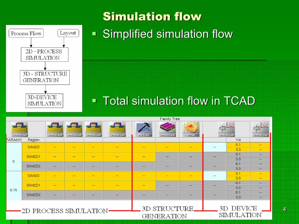
Simulation flowSimplified simulation flow
Total simulation flow in TCAD

5
2D Process simulation
2D process simulation of layout cuts SIM2D и SIM2D1
A-type transistor layout Part of the total process flow
6
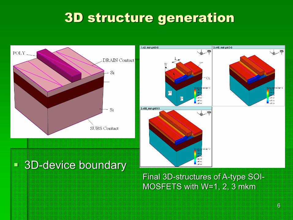
3D structure generation
3D-device boundaryFinal 3D-structures of A-type SOI-MOSFETS with W=1, 2, 3 mkm

7
Basic DC-simulation results
Front Gate: Id(Ugs)Ut=1V
BackGate: Id(Ubs)Ut=90 V
8
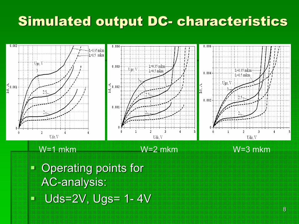
Simulated output DC- characteristics
Operating points for AC-analysis:Uds=2V, Ugs= 1- 4V
W=1 mkm W=2 mkm W=3 mkm

9
Results of АС-frequency analysis
H21(f), MUG(f) for transistors with L=0.35 mkm and W=1,2,3 mkm
H21(f), MUG(f) for transistors with L=0.5 mkmand W=1,2,3 mkm
10
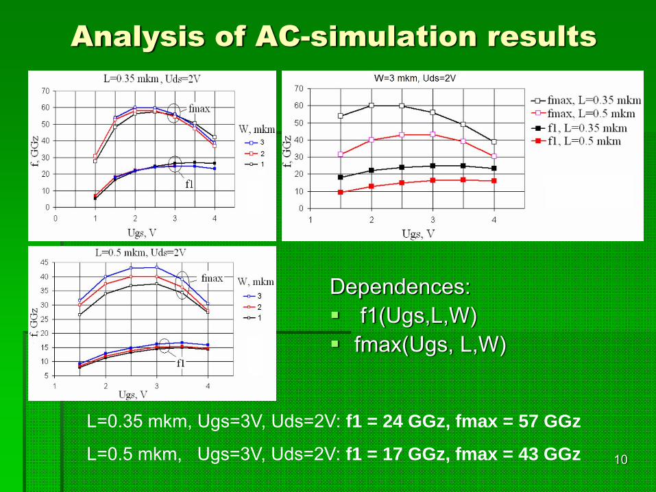
Analysis of AC-simulation results
Dependences:f1(Ugs,L,W)fmax(Ugs, L,W)
L=0.35 mkm, Ugs=3V, Uds=2V: f1 = 24 GGz, fmax = 57 GGz
L=0.5 mkm, Ugs=3V, Uds=2V: f1 = 17 GGz, fmax = 43 GGz

11
Simulation of total dose effects
Positive charge trapping occurs in oxides of SOI-structure, changing the potential distribution
Define maximum concentration of neutral traps in oxide (Ctrap). This value strongly depends on oxide fabrication conditions
Potential distribution in A-type SOI-MOSFET before and during radiation. Uds=2V Ugs=0

12
Publications about charge trapping in oxides during irradiation
Dependence of bulk trapped chargedensity versus total dose Ctrap(Dose)in BESOI with Dox=400 nm
Dependence of surface trapped charge density versus total dose in different oxides Qtrap(Dose)
R.K. Lawrence et. al, “Positive charge trapping in SOI materials”, Proc. IEEE Intern. SOI Conf., 1996, p.34
Ctrap=Qtrap/Dox
13
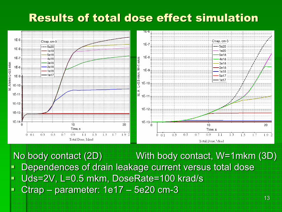
Results of total dose effect simulation
No body contact (2D) With body contact, W=1mkm (3D)Dependences of drain leakage current versus total dose Uds=2V, L=0.5 mkm, DoseRate=100 krad/sCtrap – parameter: 1e17 – 5e20 cm-3
14
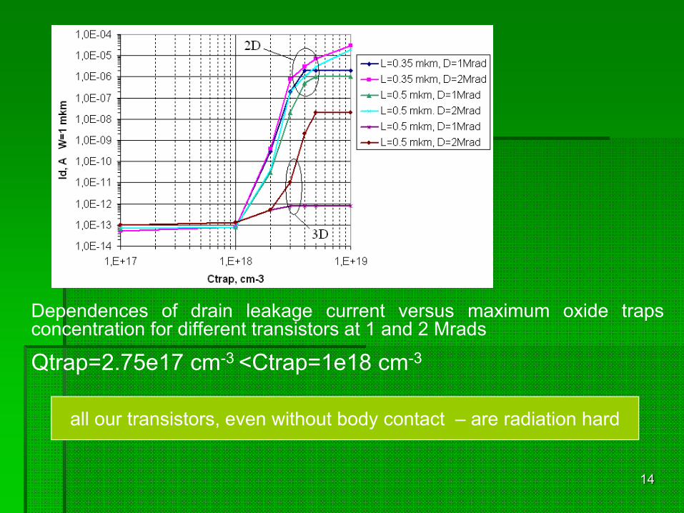
Dependences of drain leakage current versus maximum oxide trapsconcentration for different transistors at 1 and 2 Mrads
Qtrap=2.75e17 cm-3 <Ctrap=1e18 cm-3
all our transistors, even without body contact – are radiation hard

15
Thank You!


